KR101394925B1 - Liquid crystal display device and driving method thereof - Google Patents
Liquid crystal display device and driving method thereofDownload PDFInfo
- Publication number
- KR101394925B1 KR101394925B1KR1020070057128AKR20070057128AKR101394925B1KR 101394925 B1KR101394925 B1KR 101394925B1KR 1020070057128 AKR1020070057128 AKR 1020070057128AKR 20070057128 AKR20070057128 AKR 20070057128AKR 101394925 B1KR101394925 B1KR 101394925B1
- Authority
- KR
- South Korea
- Prior art keywords
- gate
- data
- signal
- liquid crystal
- voltage
- Prior art date
- Legal status (The legal status is an assumption and is not a legal conclusion. Google has not performed a legal analysis and makes no representation as to the accuracy of the status listed.)
- Active
Links
Images


Classifications
- G—PHYSICS
- G09—EDUCATION; CRYPTOGRAPHY; DISPLAY; ADVERTISING; SEALS
- G09G—ARRANGEMENTS OR CIRCUITS FOR CONTROL OF INDICATING DEVICES USING STATIC MEANS TO PRESENT VARIABLE INFORMATION
- G09G3/00—Control arrangements or circuits, of interest only in connection with visual indicators other than cathode-ray tubes
- G09G3/20—Control arrangements or circuits, of interest only in connection with visual indicators other than cathode-ray tubes for presentation of an assembly of a number of characters, e.g. a page, by composing the assembly by combination of individual elements arranged in a matrix no fixed position being assigned to or needed to be assigned to the individual characters or partial characters
- G09G3/34—Control arrangements or circuits, of interest only in connection with visual indicators other than cathode-ray tubes for presentation of an assembly of a number of characters, e.g. a page, by composing the assembly by combination of individual elements arranged in a matrix no fixed position being assigned to or needed to be assigned to the individual characters or partial characters by control of light from an independent source
- G09G3/36—Control arrangements or circuits, of interest only in connection with visual indicators other than cathode-ray tubes for presentation of an assembly of a number of characters, e.g. a page, by composing the assembly by combination of individual elements arranged in a matrix no fixed position being assigned to or needed to be assigned to the individual characters or partial characters by control of light from an independent source using liquid crystals
- G09G3/3607—Control arrangements or circuits, of interest only in connection with visual indicators other than cathode-ray tubes for presentation of an assembly of a number of characters, e.g. a page, by composing the assembly by combination of individual elements arranged in a matrix no fixed position being assigned to or needed to be assigned to the individual characters or partial characters by control of light from an independent source using liquid crystals for displaying colours or for displaying grey scales with a specific pixel layout, e.g. using sub-pixels
- G—PHYSICS
- G09—EDUCATION; CRYPTOGRAPHY; DISPLAY; ADVERTISING; SEALS
- G09G—ARRANGEMENTS OR CIRCUITS FOR CONTROL OF INDICATING DEVICES USING STATIC MEANS TO PRESENT VARIABLE INFORMATION
- G09G3/00—Control arrangements or circuits, of interest only in connection with visual indicators other than cathode-ray tubes
- G09G3/20—Control arrangements or circuits, of interest only in connection with visual indicators other than cathode-ray tubes for presentation of an assembly of a number of characters, e.g. a page, by composing the assembly by combination of individual elements arranged in a matrix no fixed position being assigned to or needed to be assigned to the individual characters or partial characters
- G09G3/34—Control arrangements or circuits, of interest only in connection with visual indicators other than cathode-ray tubes for presentation of an assembly of a number of characters, e.g. a page, by composing the assembly by combination of individual elements arranged in a matrix no fixed position being assigned to or needed to be assigned to the individual characters or partial characters by control of light from an independent source
- G09G3/36—Control arrangements or circuits, of interest only in connection with visual indicators other than cathode-ray tubes for presentation of an assembly of a number of characters, e.g. a page, by composing the assembly by combination of individual elements arranged in a matrix no fixed position being assigned to or needed to be assigned to the individual characters or partial characters by control of light from an independent source using liquid crystals
- G09G3/3611—Control of matrices with row and column drivers
- G09G3/3614—Control of polarity reversal in general
- G—PHYSICS
- G09—EDUCATION; CRYPTOGRAPHY; DISPLAY; ADVERTISING; SEALS
- G09G—ARRANGEMENTS OR CIRCUITS FOR CONTROL OF INDICATING DEVICES USING STATIC MEANS TO PRESENT VARIABLE INFORMATION
- G09G3/00—Control arrangements or circuits, of interest only in connection with visual indicators other than cathode-ray tubes
- G09G3/20—Control arrangements or circuits, of interest only in connection with visual indicators other than cathode-ray tubes for presentation of an assembly of a number of characters, e.g. a page, by composing the assembly by combination of individual elements arranged in a matrix no fixed position being assigned to or needed to be assigned to the individual characters or partial characters
- G09G3/34—Control arrangements or circuits, of interest only in connection with visual indicators other than cathode-ray tubes for presentation of an assembly of a number of characters, e.g. a page, by composing the assembly by combination of individual elements arranged in a matrix no fixed position being assigned to or needed to be assigned to the individual characters or partial characters by control of light from an independent source
- G09G3/36—Control arrangements or circuits, of interest only in connection with visual indicators other than cathode-ray tubes for presentation of an assembly of a number of characters, e.g. a page, by composing the assembly by combination of individual elements arranged in a matrix no fixed position being assigned to or needed to be assigned to the individual characters or partial characters by control of light from an independent source using liquid crystals
- G09G3/3611—Control of matrices with row and column drivers
- G09G3/3674—Details of drivers for scan electrodes
- G—PHYSICS
- G09—EDUCATION; CRYPTOGRAPHY; DISPLAY; ADVERTISING; SEALS
- G09G—ARRANGEMENTS OR CIRCUITS FOR CONTROL OF INDICATING DEVICES USING STATIC MEANS TO PRESENT VARIABLE INFORMATION
- G09G3/00—Control arrangements or circuits, of interest only in connection with visual indicators other than cathode-ray tubes
- G09G3/20—Control arrangements or circuits, of interest only in connection with visual indicators other than cathode-ray tubes for presentation of an assembly of a number of characters, e.g. a page, by composing the assembly by combination of individual elements arranged in a matrix no fixed position being assigned to or needed to be assigned to the individual characters or partial characters
- G09G3/34—Control arrangements or circuits, of interest only in connection with visual indicators other than cathode-ray tubes for presentation of an assembly of a number of characters, e.g. a page, by composing the assembly by combination of individual elements arranged in a matrix no fixed position being assigned to or needed to be assigned to the individual characters or partial characters by control of light from an independent source
- G09G3/36—Control arrangements or circuits, of interest only in connection with visual indicators other than cathode-ray tubes for presentation of an assembly of a number of characters, e.g. a page, by composing the assembly by combination of individual elements arranged in a matrix no fixed position being assigned to or needed to be assigned to the individual characters or partial characters by control of light from an independent source using liquid crystals
- G09G3/3611—Control of matrices with row and column drivers
- G09G3/3685—Details of drivers for data electrodes
- G—PHYSICS
- G09—EDUCATION; CRYPTOGRAPHY; DISPLAY; ADVERTISING; SEALS
- G09G—ARRANGEMENTS OR CIRCUITS FOR CONTROL OF INDICATING DEVICES USING STATIC MEANS TO PRESENT VARIABLE INFORMATION
- G09G2300/00—Aspects of the constitution of display devices
- G09G2300/08—Active matrix structure, i.e. with use of active elements, inclusive of non-linear two terminal elements, in the pixels together with light emitting or modulating elements
- G09G2300/0809—Several active elements per pixel in active matrix panels
- G09G2300/0823—Several active elements per pixel in active matrix panels used to establish symmetry in driving, e.g. with polarity inversion
- G—PHYSICS
- G09—EDUCATION; CRYPTOGRAPHY; DISPLAY; ADVERTISING; SEALS
- G09G—ARRANGEMENTS OR CIRCUITS FOR CONTROL OF INDICATING DEVICES USING STATIC MEANS TO PRESENT VARIABLE INFORMATION
- G09G2310/00—Command of the display device
- G09G2310/02—Addressing, scanning or driving the display screen or processing steps related thereto
- G09G2310/0264—Details of driving circuits
- G09G2310/0286—Details of a shift registers arranged for use in a driving circuit
- G—PHYSICS
- G09—EDUCATION; CRYPTOGRAPHY; DISPLAY; ADVERTISING; SEALS
- G09G—ARRANGEMENTS OR CIRCUITS FOR CONTROL OF INDICATING DEVICES USING STATIC MEANS TO PRESENT VARIABLE INFORMATION
- G09G2310/00—Command of the display device
- G09G2310/02—Addressing, scanning or driving the display screen or processing steps related thereto
- G09G2310/0264—Details of driving circuits
- G09G2310/0289—Details of voltage level shifters arranged for use in a driving circuit
- G—PHYSICS
- G09—EDUCATION; CRYPTOGRAPHY; DISPLAY; ADVERTISING; SEALS
- G09G—ARRANGEMENTS OR CIRCUITS FOR CONTROL OF INDICATING DEVICES USING STATIC MEANS TO PRESENT VARIABLE INFORMATION
- G09G2330/00—Aspects of power supply; Aspects of display protection and defect management
- G09G2330/02—Details of power systems and of start or stop of display operation
- G09G2330/021—Power management, e.g. power saving
- H—ELECTRICITY
- H03—ELECTRONIC CIRCUITRY
- H03M—CODING; DECODING; CODE CONVERSION IN GENERAL
- H03M1/00—Analogue/digital conversion; Digital/analogue conversion
- H03M1/66—Digital/analogue converters
Landscapes
- Engineering & Computer Science (AREA)
- Chemical & Material Sciences (AREA)
- Crystallography & Structural Chemistry (AREA)
- Physics & Mathematics (AREA)
- Computer Hardware Design (AREA)
- General Physics & Mathematics (AREA)
- Theoretical Computer Science (AREA)
- Control Of Indicators Other Than Cathode Ray Tubes (AREA)
Abstract
Translated fromKoreanDescription
Translated fromKorean도 1은 본 발명의 제 1 실시 예에 따른 액정 표시장치를 나타내는 도면.1 is a view showing a liquid crystal display device according to a first embodiment of the present invention.
도 2는 도 1에 도시된 구동 집적회로를 나타내는 도면.Fig. 2 is a view showing the driving integrated circuit shown in Fig. 1. Fig.
도 3은 도 1에 도시된 게이트 구동회로를 구동하기 위한 게이트 구동신호를 나타내는 파형도.3 is a waveform diagram showing a gate driving signal for driving the gate driving circuit shown in Fig.
도 4는 도 1에 도시된 게이트 구동회로를 나타내는 도면.4 is a view showing the gate drive circuit shown in Fig.
도 5는 본 발명의 제 1 실시 예에 따른 액정 표시장치의 구동방법을 나타내는 파형도.5 is a waveform diagram showing a driving method of a liquid crystal display according to a first embodiment of the present invention;
도 6 및 도 7은 본 발명의 실시 예에 따른 액정 표시장치의 액정패널에 표시되는 화상신호의 극성패턴을 나타내는 도면.6 and 7 are views showing polar patterns of image signals displayed on a liquid crystal panel of a liquid crystal display device according to an embodiment of the present invention.
도 8은 본 발명의 제 2 실시 예에 따른 액정 표시장치를 나타내는 도면.8 is a view showing a liquid crystal display device according to a second embodiment of the present invention.
도 9는 도 8에 도시된 제 1 및 제 2 게이트 구동회로를 나타내는 도면.9 is a view showing first and second gate driving circuits shown in Fig.
< 도면의 주요 부분에 대한 부호설명 >Description of the Related Art [0002]
100 : 액정패널 102 : 하부기판100: liquid crystal panel 102: lower substrate
104 : 상부기판 110 : 화소셀104: upper substrate 110: pixel cell
112 : 박막 트랜지스터 114 : 화소전극112: thin film transistor 114: pixel electrode
120 : 게이트 구동회로 130 : 구동 집적회로120: gate driving circuit 130: driving integrated circuit
200 : 가요성 인쇄회로200: flexible printed circuit
본 발명은 액정 표시장치에 관한 것으로, 특히 데이터의 충전특성을 향상시킬 수 있도록 한 액정 표시장치 및 그의 구동방법에 관한 것이다.BACKGROUND OF THE
일반적으로 액정 표시장치는 전계를 이용하여 액정의 광 투과율을 조절함으로써 화상을 표시하게 된다.In general, a liquid crystal display device displays an image by adjusting the light transmittance of a liquid crystal using an electric field.
이를 위해, 액정 표시장치는 두 장의 유리기판 사이에 액정이 형성되고 매트릭스 형태로 배열된 화소셀들과 화소셀들에 공급되는 신호를 절환하기 위한 스위치 소자들로 구성된 액정패널과, 액정패널을 구동하기 위한 구동 회로부와, 액정패널에 광을 조사하는 백 라이트 유닛(Back Light Unit)을 포함하여 구성된다.To this end, a liquid crystal display device includes a liquid crystal panel composed of pixel cells in which liquid crystal is formed between two glass substrates and arranged in a matrix form, and switch elements for switching signals supplied to the pixel cells, And a back light unit (back light unit) for irradiating light to the liquid crystal panel.
최근 액정패널의 신호라인 수 또는 회로 부품의 수를 감소시켜 얇고 가벼움과 동시에 저렴한 액정 표시장치가 개발되고 있다. 이에 따라 대한민국 공개특허공보 2003-39972호에서는 표시 영역의 주변 영역에 액정패널을 구동하는 하나의 통합 구동 칩을 장착함으로써 칩을 장착하는데 소요되는 공정시간 및 불량율을 감소시킬 수 있고, 더불어 전체적인 사이즈를 줄일 수 있는 온 글라스 싱글칩 액정 표시장치가 제안되었다.In recent years, the number of signal lines or the number of circuit components of a liquid crystal panel has been reduced, so that a thin, light and inexpensive liquid crystal display device has been developed. Accordingly, Korean Unexamined Patent Application Publication No. 2003-39972 discloses that by installing one integrated driving chip for driving the liquid crystal panel in the peripheral area of the display area, it is possible to reduce the process time and the defect rate required for mounting the chip, On glass single chip liquid crystal display device has been proposed.
그러나, 온 글라스 싱글칩 액정 표시장치는 다음과 같은 문제점이 있다.However, the on-glass single chip liquid crystal display has the following problems.
첫째, 단위 화소를 구성하는 서로 다른 컬러 픽셀들이 액정패널의 수평방향(게이트 라인 방향)으로 배치되는 수직 스트라이프 구조를 가짐으로써 액정패널에 화상신호를 공급하는 데이터 라인의 수가 많은 단점이 있다.First, there is a disadvantage in that the number of data lines supplying image signals to the liquid crystal panel is large because the different color pixels constituting the unit pixels are arranged in the horizontal direction (gate line direction) of the liquid crystal panel.
둘째, 데이터 라인 수의 증가로 인하여 통합 구동 칩의 크기가 증가하게 되므로 소형(예를 들어 360×160의 해상도) 액정패널 이외에는 적용할 수 없다는 문제점이 있다.Second, since the size of the integrated driving chip is increased due to an increase in the number of data lines, there is a problem in that it can not be applied to a small size (for example, a 360 × 160 resolution) liquid crystal panel.
셋째, 데이터 라인 수를 감소시키기 위하여 선택회로와 같은 추가적인 회로가 필요하다는 단점이 있다.Third, there is a disadvantage that an additional circuit such as a selection circuit is required to reduce the number of data lines.
넷째, 게이트 라인의 액티브 구간 동안 선택회로를 이용하여 아날로그 픽셀 데이터를 시분할하여 복수의 데이터 라인에 공급함으로써 픽셀 데이터의 충전시간이 감소하며, 픽셀 데이터의 충전시간을 고려하여 액정패널의 해상도를 설계해야만 하는 문제점이 있다.Fourth, during the active period of the gate line, the analog pixel data is supplied to the plurality of data lines by time division using the selection circuit to reduce the charging time of the pixel data, and the resolution of the liquid crystal panel must be designed in consideration of the charging time of the pixel data .
다섯째, 통합 구동 칩의 각 채널로부터 출력되는 아날로그 픽셀 데이터를 수평라인 단위로 반전시킴으로써 소비전력이 높다는 문제점이 있다.Fifth, there is a problem that power consumption is high by inverting the analog pixel data output from each channel of the integrated driving chip in units of horizontal lines.
따라서 상기와 같은 문제점을 해결하기 위하여, 본 발명은 데이터의 충전특성을 향상시킬 수 있도록 한 액정 표시장치 및 그의 구동방법을 제공하는데 있다.SUMMARY OF THE INVENTION Accordingly, the present invention has been made keeping in mind the above problems occurring in the prior art, and an object of the present invention is to provide a liquid crystal display device and a method of driving the same.
또한, 본 발명은 구조를 간소화함과 아울러 소비전력을 감소시킬 수 있도록 한 액정 표시장치 및 그의 구동방법을 제공하는데 있다.The present invention also provides a liquid crystal display device and a method of driving the same that can simplify the structure and reduce power consumption.
상기와 같은 기술적 과제를 달성하기 위한 본 발명의 실시 예에 따른 액정 표시장치는 1 수평구간을 서로 다른 단색 화상을 표시하는 제 1 내지 3 서브구간으로 나누어 컬러 화상을 표시하도록 n개의 게이트 라인과 m개의 데이터 라인에 의해 정의되는 영역마다 화소셀이 형성된 표시부와, 표시부의 상부 및 하부 각각에 형성된 상부 및 하부 더미 게이트 라인들을 가지는 액정패널; 상기 액정패널에 형성되어 상기 각 게이트 라인을 구동하는 게이트 구동회로; 및 상기 게이트 구동회로를 제어하며 상기 각 데이터 라인을 통해 상기 각 화소셀에 화상신호를 공급함과 아울러 상기 상부 및 하부 더미 게이트 라인 각각의 구동시 더미전압을 상기 각 데이터 라인에 공급하는 구동 집적회로를 포함하여 구성되는 것을 특징으로 한다.According to an aspect of the present invention, there is provided a liquid crystal display device including n gate lines for displaying a color image by dividing one horizontal section into first to third sub- A liquid crystal panel having upper and lower dummy gate lines formed on upper and lower portions of the display unit, respectively; A gate driving circuit formed on the liquid crystal panel for driving the gate lines; And a driving integrated circuit controlling the gate driving circuit to supply an image signal to each pixel cell through each of the data lines and supplying a dummy voltage to each of the data lines when each of the upper and lower dummy gate lines is driven And the like.
본 발명의 실시 예에 따른 액정 표시장치의 구동방법은 n개의 게이트 라인과 m개의 데이터 라인에 의해 정의되는 영역마다 화소셀이 형성된 표시부를 가지는 액정패널을 포함하는 액정 표시장치의 구동방법에 있어서, 상기 표시부의 상부 및 하부 각각에 형성된 상부 및 하부 더미 게이트 라인 각각에 게이트 온 전압을 공급하는 단계; 상기 상부 및 하부 더미 게이트 라인 각각에 공급되는 상기 게이트 온 전압에 따라 상기 각 데이터 라인을 더미전압으로 예비충전하는 단계; 1 수평구간을 서로 다른 단색 화상을 표시하는 제 1 내지 3 서브구간으로 나누고 각 서브구간에 대응되는 서브구간 데이터를 생성하는 단계; 상기 n개의 게이트 라인들에 게이트 온 전압을 순차적으로 공급하는 단계; 및 상기 서브구간 데이터를 화상신호로 변환하고 상기 n개의 게이트 라인 각각에 공급되는 상기 게이트 온 전압에 따라 상기 화상신호를 상기 각 데이터 라인을 통해 상기 각 화소셀에 공급하는 단계를 포함하 여 이루어진 것을 특징으로 한다.A driving method of a liquid crystal display according to an embodiment of the present invention is a driving method of a liquid crystal display including a liquid crystal panel having a display unit in which pixel cells are formed for each region defined by n gate lines and m data lines, Supplying a gate-on voltage to upper and lower dummy gate lines formed on upper and lower portions of the display unit, respectively; Pre-charging each of the data lines with a dummy voltage according to the gate-on voltage supplied to each of the upper and lower dummy gate lines; Dividing one horizontal section into first to third sub-sections for displaying different monochrome images, and generating sub-section data corresponding to each sub-section; Sequentially supplying a gate-on voltage to the n gate lines; And a step of converting the sub-section data into an image signal and supplying the image signal to each of the pixel cells through the data lines in accordance with the gate-on voltage supplied to each of the n gate lines .
이하, 첨부된 도면 및 실시 예를 통해 본 발명의 실시 예를 구체적으로 살펴보면 다음과 같다.Hereinafter, exemplary embodiments of the present invention will be described in detail with reference to the accompanying drawings and embodiments.
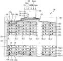
도 1은 본 발명의 제 1 실시 예에 따른 액정 표시장치를 나타내는 도면이다.1 is a view showing a liquid crystal display device according to a first embodiment of the present invention.
도 1을 참조하면, 본 발명의 제 1 실시 예에 따른 액정 표시장치는 1 수평구간을 서로 다른 단색 화상을 표시하는 제 1 내지 3 서브구간으로 나누어 컬러 화상을 표시하도록 n개의 게이트 라인(GL1 내지 GLn)과 m개의 데이터 라인(DL1 내지 DLm)에 의해 정의되는 영역마다 화소셀(110)이 형성된 표시부와, 표시부의 상부 및 하부 각각에 형성된 상부 및 하부 더미 게이트 라인들(GL0, GLn+1)을 가지는 액정패널(100)과, 액정패널(100)에 형성되어 각 게이트 라인(GL0 내지 GLn+1)을 구동하는 게이트 구동회로(120)와, 게이트 구동회로(120)를 제어하며 각 데이터 라인(DL1 내지 DLm)에 화상신호를 공급함과 아울러 상부 및 하부 더미 게이트 라인(GL0, GLn+1) 각각의 구동시 더미전압을 각 데이터 라인(DL1 내지 DLm)에 공급하는 구동 집적회로(130)와, 액정패널(100)에 부착되어 구동 집적회로(130)를 외부의 구동 시스템(미도시)에 연결하는 가요성 인쇄회로(200)를 포함하여 구성된다.Referring to FIG. 1, the liquid crystal display according to the first embodiment of the present invention includes n gate lines GL1 to GLn to display one color image by dividing one horizontal section into first to third sub- GLn + 1) formed on the upper and lower portions of the display unit, and a display unit on which the
액정패널(100)은 서로 대향하도록 합착된 하부기판(102) 및 상부기판(104)과, 두 기판(102, 104) 사이의 셀갭을 일정하게 유지시키기 위한 스페이서(미도시)와, 스페이서에 의해 마련된 공간에 형성된 액정층(미도시)을 포함하여 구성된다.The
하부기판(102)은 상부기판(104)에 대응되는 표시부와 표시부를 제외한 비표시부를 포함하여 구성된다.The
하부기판(102)의 표시부에는 일정한 간격을 가지도록 제 1 방향(수직방향)으로 나란하게 형성된 m개의 데이터 라인(DL1 내지 DLm)과, 일정한 간격을 가지도록 제 1 방향과 교차되는 제 2 방향(수평방향)으로 나란하게 형성된 n개의 게이트 라인(GL1 내지 GLn)과, 복수의 데이터 라인들(DL1 내지 DLm) 및 게이트 라인들(GL1 내지 GLn)에 의해 정의되는 영역마다 형성된 화소셀(110)이 형성된다. 이때, 화상신호가 공급되는 데이터 라인들(DL1 내지 DLm)은 게이트 온 전압이 공급되는 게이트 라인들(GL)보다 적은 수를 갖는다.In the display portion of the
화소셀(110) 각각은 게이트 라인(GL1 내지 GLn)과 데이터 라인(DL1 내지 DLm)에 접속되는 박막 트랜지스터(112)와, 박막 트랜지스터(112)에 접속된 화소전극(114)을 포함하여 구성된다.Each of the
박막 트랜지스터(112)는 게이트 라인(GL1 내지 GLn)에 접속된 게이트전극과, 데이터 라인(DL1 내지 DLm)에 접속된 소스전극과, 화소전극(114)에 접속된 드레인전극을 포함하여 구성된다. 이에 따라, 박막 트랜지스터(112) 각각은 게이트 라인(GL)에 공급되는 게이트 온 전압에 따라 스위칭되어 각 데이터 라인(DL1 내지 DLm)으로부터 공급되는 화상신호를 각 화소전극(114)에 공급한다.The
화소전극(114)은 데이터 라인(DL1 내지 DLm)과 나란한 단변의 길이가 게이트 라인(GL1 내지 GLn)과 나란한 장변보다 상대적으로 짧게 형성된다. 이에 따라, 화소전극(114)은 수평 스트라이프 형태를 갖는다.The length of the short side of the
또한, 하부기판(102)에는 표시부의 상부에 형성되어 제 1 게이트 라인(GL1)의 구동 이전에 구동되는 상부 더미 게이트 라인(GL0)과, 상부 더미 게이트 라 인(GL0)과 데이터 라인들(DL1 내지 DLm)에 의해 정의되는 영역마다 형성된 상부 더미 화소셀(510a)과, 표시부의 하부에 형성되어 제 n 게이트 라인(GLn)의 구동 후에 구동되는 하부 더미 게이트 라인(GLn+1)과, 하부 더미 게이트 라인(GLn+1)과 데이터 라인들(DL1 내지 DLm)에 의해 정의되는 영역마다 형성된 하부 더미 화소셀(510b)이 더 형성된다. 이때, 상부 및 하부 더미 게이트 라인(GL0, GLn+1), 상부 및 하부 더미 화소셀(510a, 510b)은 액정패널(100)의 비표시부에 형성되거나 차광층(미도시)과 중첩되도록 형성될 수 있다.The
상부 더미 화소셀(510a)은 상부 더미 게이트 라인(GL0)과 각 데이터 라인(DL1 내지 DLm)에 접속되는 상부 더미 박막 트랜지스터(512a)와, 각 상부 더미 박막 트랜지스터(512a)에 접속된 상부 더미 화소전극(514a)을 포함하여 구성된다. 이러한, 상부 더미 화소전극(514a)은 표시부에 형성된 화소셀(110)의 화소전극(114)과 동일한 크기를 가지거나 작은 크기를 갖는다.The upper
마찬가지로, 하부 더미 화소셀(510b)은 하부 더미 게이트 라인(GLn+1)과 각 데이터 라인(DL1 내지 DLm)에 접속되는 하부 더미 박막 트랜지스터(512b)와, 각 하부 더미 박막 트랜지스터(512b)에 접속된 하부 더미 화소전극(514b)을 포함하여 구성된다. 이러한, 하부 더미 화소전극(514b)은 상부 더미 화소전극(514a)과 동일한 형태를 갖는다.Similarly, the lower
하부기판(102)의 비표시부에는 각 게이트 라인(GL0 내지 GLn+1) 각각에 접속되는 게이트 구동회로(120)가 형성됨과 아울러 구동 집적회로(130)가 실장된다.A
상부기판(104)은 컬러필터, 공통전극, 차광층 등을 포함하여 구성된다. 여 기서, 공통전극은 액정층에 형성되는 액정에 따라 하부기판(102)에 형성될 수 있다.The
컬러필터는 적색(R) 컬러필터, 녹색(G) 컬러필터 및 청색(B) 컬러필터가 데이터 라인(DL1 내지 DLm)의 방향으로 반복적으로 형성됨과 아울러 게이트 라인(GL1 내지 GLn)의 방향을 따라 동일한 색으로 형성된다.The color filter is formed by repeatedly forming a red (R) color filter, a green (G) color filter and a blue (B) color filter in the direction of the data lines DL1 to DLm and also along the direction of the gate lines GL1 to GLn And are formed in the same color.
공통전극은 액정층에 수직 전계를 형성하기 위해 화소전극(114)과 대향되도록 상부기판(104)의 전면에 형성되거나 라인 형태로 형성될 수 있다. 여기서, 공통전극은 액정층에 수평 전계를 형성하기 위해 화소전극(114)과 나란하도록 하부기판(102)에 형성될 수 있다.The common electrode may be formed on the front surface of the
차광층은 화소전극(114)에 중첩되는 개구영역을 제외한 나머지 영역에 중첩되도록 상부기판(104) 상에 형성된다.The light shielding layer is formed on the
이러한, 적색(R) 컬러필터, 녹색(G) 컬러필터 및 청색(B) 컬러필터 각각이 형성된 적색(R), 녹색(G) 및 청색(B)의 화소셀은 하나의 컬러 화상을 표시하기 위한 단위 화소를 구성한다.The pixel cells of red (R), green (G), and blue (B) in which the red (R) color filter, the green (G) color filter and the blue Thereby forming a unit pixel.
가요성 인쇄회로(200)는 하부기판(102)의 비표시부에 마련된 패드부에 부착된다. 이러한, 가요성 인쇄회로(200)는 구동 시스템으로부터 공급되는 소스 데이터 신호(Data) 및 동기신호(DE, DCLK, Hsync, Vsync)를 구동 집적회로(130)에 전달한다.The flexible printed
구동 집적회로(130)는 복수의 입출력 패드를 가지도록 하부기판(102)의 비표시부에 형성된 집적회로 실장부에 실장된다. 이에 따라, 구동 집적회로(130)에 마 련된 각 입출력 범프들은 집적회로 실장부의 각 입출력 패드들에 전기적으로 접속되도록 실장된다.The driving integrated
구동 집적회로(130)는 가요성 인쇄회로(200)로부터 공급되는 동기신호(DE, DCLK, Hsync, Vsync) 중 적어도 하나를 이용하여 수평 동기신호(Hsync)의 한 주기에 대응되는 1 수평구간을 제 1 내지 제 3 서브구간으로 나누어 구동하기 위한 게이트 구동신호 및 데이터 제어신호를 생성한다.The driving integrated
또한, 구동 집적회로(130)는 소스 데이터 신호(Data)를 제 1 내지 제 3 서브구간 각각에 대응되는 적색 데이터(R), 녹색 데이터(G) 및 청색 데이터(B)로 정렬한 후, 아날로그 신호인 화상신호로 변환하여 데이터 라인들(DL)에 공급한다. 이때, 화상신호의 극성은 데이터 라인(DL) 단위로 반전됨과 아울러 적어도 1 프레임 단위로 반전된다.The driving
그리고, 구동 집적회로(130)는 상부 및 하부 더미 게이트 라인들(GL0, GLn+1) 각각의 구동시 더미전압을 각 데이터 라인(DL1 내지 DLm)에 공급한다. 이때, 더미전압은 현재 프레임 동안 각 데이터 라인(DL1 내지 DLm)에 공급된 화상신호의 극성과 반전되는 극성을 갖는다. 이에 따라, 각 데이터 라인(DL1 내지 DLm)은 더미전압에 의해 예비충전됨으로써 화상신호의 극성 반전에 따른 표시부의 첫번째 및 마지막 라인에 접속된 각 화소셀(110)의 충전 특성이 향상된다.The driving
도 2는 본 발명의 실시 예에 따른 구동 집적회로를 나타내는 블록도이다.2 is a block diagram showing a driving integrated circuit according to an embodiment of the present invention.
도 2를 도 1과 결부하면, 본 발명의 실시 예에 따른 구동 집적회로(130)는 신호 중계부(310), 제 1 전원 생성부(320), 클럭 생성부(322), 기준전압 설정 부(324), 제 2 전원 생성부(326), 신호 제어부(330), 제어신호 생성부(340), 승압회로(350), 계조전압 생성부(360), 공통전압 생성부(370) 및 데이터 변환부(380)를 포함하여 구성된다.2, the driving
신호 중계부(310)는 가요성 인쇄회로(200)로부터 공급되는 소스 데이터 신호(Data) 및 동기신호(DE, DCLK, Hsync, Vsync)를 신호 제어부(330)로 중계한다.The
클럭 생성부(322)는 제 1 및 제 2 전원 생성부(320, 326)를 구동시키기 위한 클럭을 생성한다.The
제 1 전원 생성부(320)는 가요성 인쇄회로(200)로부터 공급되는 입력전원(Vin)을 이용하여 클럭 생성부(322)로부터 공급되는 클럭에 따라 제 1 전원, 즉 제 1 및 제 2 기준전압(VSP, VSN)을 생성한다. 이때, 가요성 인쇄회로(200)에 실장된 저항(210)과 커패시터(220) 및 인덕터(230) 등의 수동소자는 전원 신호라인(321a, 321b, 321c)을 통해 제 1 전원 생성부(320)에 접속되어 제 1 전원 생성부(320)에서 생성된 제 1 및 제 2 기준전압(VSP, VSN)을 바이어싱(Biasing)하거나 구동 집적회로(130)의 옵션기능을 설정하기 위하여 사용된다.The
제 2 전원 생성부(326)는 제 1 전원 생성부(320)에서 생성된 제 1 및 제 2 기준전압(VSP, VSN)을 이용하여 액정패널(100)의 구동에 필요한 제 2 전원, 즉 제 1 및 제 2 구동전압(Vdd, Vss), 집적회로 구동전압(Vcc), 게이트 온 전압(Von) 및 게이트 오프 전압(Voff)을 생성한다.The second
기준전압 설정부(324)는 제 1 전원 생성부(320)로부터 계조전압 생성부(360)로 공급되는 제 1 및 제 2 기준전압(VSP, VSN)의 레벨을 설정한다.The reference
신호 제어부(330)는 신호 중계부(310)의 구동을 제어하며, 구동 집적회로(130)의 내부 회로블록을 제어하는 역할을 한다.The
또한, 신호 제어부(330)는 신호 중계부(310)로부터 공급되는 소스 데이터 신호(Data)를 액정패널(100)의 구동에 알맞도록 정렬하고, 정렬된 데이터(R, G, B)를 각 수평구간의 서브구간에 대응되도록 재정렬하여 데이터 변환부(380)에 공급한다.The
구체적으로, 신호 제어부(330)는 신호 중계부(310)로부터 공급되는 소스 데이터 신호(Data)를 액정패널(100)의 해상도에 알맞도록 정렬한다. 그리고, 신호 제어부(330)는 정렬된 1 수평구간 단위의 소스 데이터 신호(Data)의 적색, 녹색 및 청색 데이터(R, G, B)를 1 수평구간의 제 1 내지 제 3 서브구간 각각에 대응되도록 재정렬하여 데이터 변환부(380)에 공급한다. 즉, 신호 제어부(330)는 소스 데이터 신호(Data) 중 적색 데이터(R)를 1 수평구간의 제 1 서브구간 데이터로 재정렬하고, 소스 데이터 신호(Data) 중 녹색 데이터(G)를 1 수평구간의 제 2 서브구간 데이터로 재정렬하고, 소스 데이터 신호(Data) 중 청색 데이터(B)를 1 수평구간의 제 3 서브구간 데이터로 재정렬한다.Specifically, the
또한, 신호 제어부(330)는 신호 중계부(310)로부터 공급되는 동기신호(DE, DCLK, Hsync, Vsync)를 제어신호 생성부(340)로 전달한다.The
제어신호 생성부(340)는 신호 제어부(330)로부터 공급되는 동기신호(DE, DCLK, Hsync, Vsync) 중 적어도 하나를 이용하여 데이터 제어신호(DST, DSC, DOE, DPS) 및 게이트 구동신호(RVst1 내지 RVst4, RCLK1 내지 RCLK8)를 생성한다.The
데이터 제어신호(DST, DSC, DOE, DPS)는 데이터 변환부(380)를 제어하기 위 한 데이터 스타트 신호(DST)와, 데이터 쉬프트 클럭(DSC)과, 데이터 출력신호(DOE) 및 데이터 극성신호(DPS)를 포함한다. 여기서, 제어신호 생성부(340)는 화상신호의 극성을 각 데이터 라인(DL)로 반전시킴과 아울러 적어도 1 프레임 단위로 반전시키기 위한 데이터 극성신호(DPS)를 생성한다.The data control signals DST, DSC, DOE and DPS correspond to the data start signal DST for controlling the
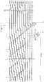
게이트 구동신호(RVst1 내지 RVst4, RCLK1 내지 RCLK8)는, 도 3에 도시된 바와 같이, 게이트 구동회로(120)를 구동시키기 위한 제 1 내지 제 4 게이트 스타트 신호(RVst1 내지 RVst4)와 제 1 내지 제 8 게이트 클럭신호(RCLK1 내지 RCLK8)를 포함한다.The gate driving signals RVst1 to RVst4 and RCLK1 to RCLK8 are input to the first to fourth gate start signals RVst1 to RVst4 for driving the
제 1 내지 제 4 게이트 스타트 신호(RVst1 내지 RVst4) 각각은 2 서브구간에 대응되는 펄스 폭(W1)을 가지며, 위상이 1 서브구간 단위로 순차 지연된다. 이때, 제 1 게이트 스타트 신호(RVst1)는 각 프레임의 제 1 수평구간(1H)의 이전 2 수평구간(T1)에서 라이징된다. 이러한, 제 1 내지 제 4 게이트 스타트 신호(RVst1 내지 RVst4)는 게이트 구동회로(120)의 구동을 개시시킨다.Each of the first to fourth gate start signals RVst1 to RVst4 has a pulse width W1 corresponding to two sub-periods, and the phases are sequentially delayed in units of one sub-interval. At this time, the first gate start signal RVst1 is increased in the previous two horizontal periods T1 of the first
제 1 내지 제 8 게이트 클럭신호(RCLK1 내지 RCLK8) 각각은 4 서브구간에 대응되는 펄스 폭(W2)을 가지며, 위상이 1 서브구간 단위로 순차 지연된다. 이때, 제 1 게이트 클럭신호(RCLK1)는 제 1 게이트 스타트 신호(Vst1)의 폴링시점에서 라이징된다. 여기서, 제 1 내지 제 8 게이트 클럭신호(RCLK1 내지 RCLK8) 각각의 라이징 시점은 게이트 펄스 폭 변조신호(미도시)에 의해 가변될 수 있다. 한편, 제 1 내지 제 4 게이트 스타트 신호(RVst1 내지 RVst4)와 제 1 내지 제 8 게이트 클럭신호(RCLK1 내지 RCLK8)는 블랭킹 구간의 리셋구간(RT)에서 리셋된다.Each of the first to eighth gate clock signals RCLK1 to RCLK8 has a pulse width W2 corresponding to four sub-intervals, and the phases are sequentially delayed in units of one sub-interval. At this time, the first gate clock signal RCLK1 is rising at the time of polling of the first gate-start signal Vst1. Here, the rising time of each of the first to eighth gate clock signals RCLK1 to RCLK8 may be varied by a gate pulse width modulation signal (not shown). Meanwhile, the first to fourth gate start signals RVst1 to RVst4 and the first to eighth gate clock signals RCLK1 to RCLK8 are reset in the reset period RT of the blanking interval.
승압회로(350)는 제 2 전원 생성부(326)로부터 공급되는 게이트 온 전압(Von) 및 게이트 오프 전압(Voff)을 이용하여 제어신호 생성부(340)로부터 공급되는 제 1 내지 제 4 게이트 스타트 신호(RVst1 내지 RVst4)와 제 1 내지 제 8 게이트 클럭신호(RCLK1 내지 RCLK8)의 전압레벨을 승압한다. 여기서, 게이트 온 전압(Von)은 각 화소셀(110)의 박막 트랜지스터(112)를 턴-온시키기 위한 전압이고, 게이트 오프 전압(Voff)은 박막 트랜지스터(112)를 턴-오프시키기 위한 전압이다. 이러한, 승압회로(350)는 하부기판(102)의 비표시부에 형성된 게이트 구동신호 전송라인(140)을 통해 승압된 제 1 내지 제 4 게이트 스타트 신호(Vst1 내지 Vst4)와 제 1 내지 제 8 게이트 클럭신호(CLK1 내지 CLK8)를 게이트 구동회로(120)에 공급한다.The boosting
공통전압 생성부(370)는 제 2 전원 생성부(326)로부터 가요성 인쇄회로(200)의 수동소자를 통해 공급되는 제 1 및 제 2 구동전압(Vdd, Vss)과 제어신호 생성부(340)로부터 공급되는 데이터 극성신호(DPS)를 이용하여 액정패널(100)의 공통전극에 공급될 공통전압(Vcom)을 생성한다.The common
계조전압 생성부(360)는 제 1 전원 생성부(320)로부터 공급되는 제 1 및 제 2 기준전압(VSP, VSN)을 복수의 계조전압으로 세분화하여 데이터 변환부(380)에 공급한다. 여기서, 계조전압 생성부(360)는 소스 데이터 신호(Data)가 N비트일 경우, 2N개의 정극성(+) 계조전압과 부극성(-) 계조전압을 생성한다.The
데이터 변환부(380)는 쉬프트 레지스터(381), 래치부(383), 디지털-아날로그 변환부(385), 버퍼부(387) 및 선택부(389)를 포함하여 구성된다.The
쉬프트 레지스터(381)는 제어신호 생성부(340)로부터 공급되는 데이터 쉬프트 클럭(DSC)에 따라 데이터 스타트 신호(DST)를 순차적으로 쉬프트시켜 쉬프트 신호(SS)를 생성한다. 이때, 쉬프트 레지스터(381)는 신호 제어부(330)로부터 공급되는 방향신호에 따라 양방향으로 구동되는 양방향 쉬프트 레지스터가 될 수 있다.The
래치부(383)는 쉬프트 레지스터(381)로부터 공급되는 쉬프트 신호(SS)에 따라 신호 제어부(330)로부터 공급되는 1 수평 라인분의 서브구간 데이터(R, G, B)를 순차적으로 래치한다. 그리고, 래치부(383)는 제어신호 생성부(340)로부터 공급되는 데이터 출력신호(DOE)에 따라 래치된 1 수평 라인분의 서브구간 데이터(Rdata)를 디지털-아날로그 변환부(385)에 공급한다.The
디지털-아날로그 변환부(385)는 계조전압 생성부(360)로부터 공급되는 복수의 정극성 계조전압들과 부극성 계조전압들을 이용하여 래치부(383)로부터 공급되는 래치된 데이터(Rdata)를 아날로그 신호인 정극성 및 부극성 화상신호(PVS, NVS)로 변환한다. 이때, 디지털-아날로그 변환부(385)는 복수의 정극성 계조전압들 중 래치된 데이터(Rdata)의 계조값에 대응되는 하나의 계조전압을 정극성 화상신호(PVS)로 선택함과 동시에 복수의 부극성 계조전압들 중 래치된 데이터(Rdata)의 계조값에 대응되는 하나의 계조전압을 부극성 화상신호(NVS)로 선택한다.The digital-
버퍼부(387)는 제 1 전원 생성부(320)로부터 가요성 인쇄회로(200)의 수동소자를 통해 공급되는 제 1 및 제 2 구동전압(Vdd, Vss)을 이용하여 정극성 및 부극성 화상신호(PVS, NVS) 각각을 버퍼링한다. 이때, 버퍼부(387)는 데이터 라인(DL) 의 부하를 감안하여 정극성 및 부극성 화상신호(PVS, NVS) 각각을 증폭하여 출력한다.The
선택부(389)는 제어신호 생성부(340)로부터 공급되는 데이터 극성신호(DPS)에 따라 버퍼부(387)로부터 공급되는 정극성 또는 부극성 화상신호(PVS, NVS)를 선택하여 데이터 라인들(DL1 내지 DLm)에 공급한다. 이때, 선택부(389)에서 출력되는 화상신호의 극성은 데이터 극성신호(DPS)에 따라 각 데이터 라인(DL) 단위로 반전됨과 아울러 적어도 1 프레임 단위로 반전된다. 이에 따라, 액정패널(100)에 공급되는 화상신호는 각 데이터 라인(DL) 단위로 반전되는 컬럼 인버젼 방식의 극성패턴을 갖는다.The
도 1에서, 게이트 구동회로(120)는 박막 트랜지스터(112)의 형성 공정과 함께 각 게이트 라인들(GL0 내지 GLn+1) 각각에 접속되도록 하부기판(102)의 비표시부에 형성된다. 이러한, 게이트 구동회로(120)는 복수의 게이트 구동신호 전송라인(140)을 통해 구동 집적회로(130)로부터 공급되는 승압된 제 1 내지 제 4 게이트 스타트 신호(Vst1 내지 Vst4)에 의해 구동 개시되어 제 1 내지 제 8 게이트 클럭신호(CLK1 내지 CLK8)에 대응되는 게이트 온 전압을 게이트 라인들(GL0 내지 GLn+1)에 순차적으로 공급한다.1, the
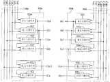
이를 위해, 게이트 구동회로(120)는, 도 4에 도시된 바와 같이, 상부 더미 스테이지(624m1), n개의 스테이지(6241 내지 624n) 및 하부 더미 스테이지(624m2)를 포함하여 구성된다. 여기서, n은 더미 게이트 라인들(GL0, GLn+1)을 제외한 게이트 라인의 총 개수를 의미한다.To this end, the
상부 더미 스테이지(624m1)는 제 1 게이트 스타트 신호(Vst1)에 의해 구동되어 제 1 게이트 클럭신호(CLK1)에 대응되는 게이트 온 전압을 상부 더미 게이트 라인(GL0) 및 제 4 스테이지(6244)에 공급한다.The upper dummy stage 624m1 is driven by the first gate start signal Vst1 to supply a gate-on voltage corresponding to the first gate clock signal CLK1 to the upper dummy gate line GL0 and the
n개의 스테이지(6241 내지 624n) 중 4i-3(단, i는 제 1 내지 n/4인 자연수)번째 스테이지(6241, 6245...)는 제 2 게이트 스타트 신호(Vst2)에 의해 구동되어 제 2 및 제 6 게이트 클럭신호(CLK2, CLK6)에 따라 클럭신호(CLK2, CLK6)에 대응되는 게이트 온 전압을 4i-3번째 게이트 라인(GL1, GL5...)에 순차적으로 공급한다. 이때, 4i-3번째 스테이지(6241, 6245...) 중 첫번째 스테이지인 제 1 스테이지(6241)는 제 2 게이트 스타트 신호(Vst2)에 의해 구동되어 제 2 게이트 클럭신호(CLK2)를 제 1 게이트 라인(GL1) 및 제 5 스테이지(6245)에 공급한다. 그리고, 4i-3번째 스테이지(6241, 6245...) 중 첫번째 스테이지(6241)를 제외한 나머지 4i+1번째 스테이지(6245...) 각각은 4i-3번째 스테이지(6241, 6245...)로부터의 출력신호에 의해 구동되어 해당 게이트 라인(GL5, GL9, GL13...)에 게이트 온 전압을 순차적으로 공급한다.The 4i-3 stages of the n stages 6241 to 624n (where i is a natural number from 1 to n / 4) are driven by the second gate start signal Vst2, The gate-on voltages corresponding to the clock signals CLK2 and CLK6 are sequentially supplied to the (4i-3) th gate lines GL1, GL5, ... according to the first and second gate clock signals CLK2 and CLK6. At this time, the
n개의 스테이지(6241 내지 624n) 중 4i-2번째 스테이지(6242...)는 제 3 게이트 스타트 신호(Vst3)에 의해 구동되어 제 3 및 제 7 게이트 클럭신호(CLK3, CLK7)에 따라 클럭신호(CLK3, CLK7)에 대응되는 게이트 온 전압을 4i-2번째 게이트 라인(GL2, GL6...)에 순차적으로 공급한다. 이때, 4i-2번째 스테이지(6242...) 중 첫번째 스테이지인 제 2 스테이지(6242)는 제 3 게이트 스타트 신호(Vst3)에 의해 구동되어 제 3 게이트 클럭신호(CLK3)를 제 2 게이트 라인(GL2) 및 제 6 스테이지 (미도시)에 공급한다. 그리고, 4i-2번째 스테이지(6242...) 중 첫번째 스테이지(6242)를 제외한 나머지 4i+2번째 스테이지(미도시) 각각은 4i-2번째 스테이지(6242...)로부터의 출력신호에 의해 구동되어 해당 게이트 라인(GL6, GL10, GL14...)에 게이트 온 전압을 순차적으로 공급한다.The 4i-
n개의 스테이지(6241 내지 624n) 중 4i-1번째 스테이지(6243...)는 제 4 게이트 스타트 신호(Vst4)에 의해 구동되어 제 4 및 제 8 게이트 클럭신호(CLK4, CLK8)에 따라 클럭신호(CLK4, CLK8)에 대응되는 게이트 온 전압을 4i-1번째 게이트 라인(GL3, GL7...)에 순차적으로 공급한다. 이때, 4i-1번째 스테이지(6243...) 중 첫번째 스테이지인 제 3 스테이지(6243)는 제 4 게이트 스타트 신호(Vst4)에 의해 구동되어 제 4 게이트 클럭신호(CLK4)를 제 3 게이트 라인(GL3) 및 제 7 스테이지(미도시)에 공급한다. 그리고, 4i-1번째 스테이지(6243...) 중 첫번째 스테이지(6243)를 제외한 나머지 4i+3번째 스테이지(미도시) 각각은 4i-1번째 스테이지(6243...)로부터의 출력신호에 의해 구동되어 해당 게이트 라인(GL7, GL11, GL15...)에 게이트 온 전압을 순차적으로 공급한다.The 4i-1
n개의 스테이지(6241 내지 624n) 중 4i번째 스테이지(6244...)는 상부 더미 스테이지(624m1)의 출력신호에 의해 구동되어 제 5 및 제 1 게이트 클럭신호(CLK5, CLK1)에 따라 클럭신호(CLK5, CLK1)에 대응되는 게이트 온 전압을 4i번째 게이트 라인(GL4, GL8...)에 순차적으로 공급한다. 이때, 4i번째 스테이지(6244...) 중 첫번째 스테이지인 제 4 스테이지(6244)는 상부 더미 스테이지(624m1)의 출력신호에 의해 구동되어 제 5 게이트 클럭신호(CLK5)를 제 4 게이트 라인(GL4) 및 제 8 스테이지(미도시)에 공급한다. 그리고, 4i번째 스테이지(6244...) 중 첫번째 스테이지(6244)를 제외한 나머지 4i+4번째 스테이지(미도시) 각각은 4i번째 스테이지(6244...)로부터의 출력신호에 의해 구동되어 해당 게이트 라인(GL8, GL12, GL16...)에 게이트 온 전압을 순차적으로 공급한다.The 4i-
하부 더미 스테이지(624m2)는 제 n-3 스테이지(624n-3)의 출력신호에 의해 구동되어 제 2 게이트 클럭신호(CLK2)에 대응되는 게이트 온 전압을 하부 더미 게이트 라인(GLn+1)에 공급한다.The lower dummy stage 624m2 is driven by the output signal of the (n-3)
도 5는 본 발명의 실시 예에 따른 액정 표시장치의 구동방법을 나타내는 파형도이다.5 is a waveform diagram showing a driving method of a liquid crystal display according to an embodiment of the present invention.
도 5를 도 1과 결부하여 본 발명의 실시 예에 따른 액정 표시장치의 구동방법을 설명하면 다음과 같다.Referring to FIG. 5, a driving method of a liquid crystal display according to an embodiment of the present invention will be described with reference to FIG.
먼저, 게이트 구동회로(120)는 구동 집적회로(130)로부터 공급되는 제 1 내지 제 4 게이트 스타트 신호(Vst1 내지 Vst4)와 4 서브구간의 펄스 폭을 가지는 제 1 내지 제 8 게이트 클럭신호(CLK1 내지 CLK8)에 따라 제 1 수평구간(1H)의 시작구간(T2)의 이전 4 서브구간(T1)에서부터 1 수평구간 단위로 중첩되도록 1 서브구간 단위로 쉬프트되는 게이트 온 전압을 각 게이트 라인(GL0 내지 GLn+1)에 순차적으로 공급한다.First, the
제 1 수평구간(1H)의 이전 1 서브구간에 있어서, 구동 집적회로(130)는 상부 더미 게이트 라인(GL0)에 공급되는 게이트 온 전압에 동기되도록 더미전압(DD)을 각 데이터 라인(DL)에 공급한다. 이에 따라, 상부 더미 게이트 라인(GL0)에 접속 된 각 상부 더미 화소셀(510a) 각각은 더미전압(DD)을 충전한다. 결과적으로, 제 1 수평구간(1H)의 이전 1 서브구간 동안, 각 데이터 라인(DL)은 이전 프레임 동안 각 화소셀(110)에 공급된 화상신호의 극성과 반전되는 극성을 가지는 더미전압(DD)으로 충전된다. 이와 동시에, 1 서브구간 단위로 위상 지연되는 게이트 온 전압에 의해 제 1 내지 제 3 게이트 라인(GL1, GL2, GL3) 각각에 접속된 각 화소셀(110)은 더미전압(DD)을 예비충전한다.The
제 1 수평구간(1H)의 제 1 서브구간(1ST)에 있어서, 구동 집적회로(130)는 제 1 게이트 라인(GL1)에 공급되는 게이트 온 전압에 동기되도록 각 데이터 라인(DL) 단위로 극성이 반전되는 적색(R) 화상신호(Vdata)를 각 데이터 라인(DL)에 공급한다. 이에 따라, 제 1 게이트 라인(GL1)에 접속되어 더미전압(DD)으로 예비충전된 각 화소셀(110) 각각은 적색(R) 화상신호(Vdata)를 본충전하여 적색(R) 화상을 표시한다. 이와 동시에, 1 서브구간 단위로 위상 지연되는 게이트 온 전압에 의해 제 2 및 제 3 게이트 라인(GL2, GL3) 각각에 접속되어 더미전압(DD)으로 예비충전된 각 화소셀(110)은 적색(R) 화상신호(Vdata)를 재충전하고, 제 4 게이트 라인(GL4)에 접속된 각 화소셀(110)은 적색(R) 화상신호(Vdata)를 예비충전한다.In the first sub-section 1ST of the first
제 1 수평구간(1H)의 제 2 서브구간(2ST)에 있어서, 구동 집적회로(130)는 제 2 게이트 라인(GL2)에 공급되는 게이트 온 전압에 동기되도록 제 1 서브구간(1ST)과 동일한 극성을 가지는 녹색(G) 화상신호(Vdata)를 각 데이터 라인(DL)에 공급한다. 이에 따라, 제 2 게이트 라인(GL2)에 접속되어 적색(R) 화상신호(Vdata)로 예비충전된 각 화소셀(110) 각각은 녹색(G) 화상신호(Vdata)를 본충전 하여 녹색(G) 화상을 표시한다. 이와 동시에, 1 서브구간 단위로 위상 지연되는 게이트 온 전압에 의해 제 3 및 제 4 게이트 라인(GL3, GL4) 각각에 접속되어 적색(R) 화상신호(Vdata)로 예비충전된 각 화소셀(110)은 녹색(G) 화상신호(Vdata)를 재충전하고, 제 5 게이트 라인(GL5)에 접속된 각 화소셀(110)은 녹색(G) 화상신호(Vdata)를 예비충전한다.In the second sub-section 2ST of the first
제 1 수평구간(1H)의 제 3 서브구간(3ST)에 있어서, 구동 집적회로(130)는 제 3 게이트 라인(GL3)에 공급되는 게이트 온 전압에 동기되도록 제 2 서브구간(2ST)과 동일한 극성을 가지는 청색(B) 화상신호(Vdata)를 각 데이터 라인(DL)에 공급한다. 이에 따라, 제 3 게이트 라인(GL3)에 접속되어 녹색(G) 화상신호(Vdata)로 예비충전된 각 화소셀(110) 각각은 청색(B) 화상신호(Vdata)를 본충전하여 청색(B) 화상을 표시한다. 이와 동시에, 1 서브구간 단위로 위상 지연되는 게이트 온 전압에 의해 제 4 및 제 5 게이트 라인(GL4, GL5) 각각에 접속되어 녹색(G) 화상신호(Vdata)로 예비충전된 각 화소셀(110)은 청색(B) 화상신호(Vdata)를 재충전하고, 제 6 게이트 라인(GL6)에 접속된 각 화소셀(110)은 청색(B) 화상신호(Vdata)를 예비충전한다.In the third sub-section 3ST of the first
이와 같은, 제 1 수평구간(1H)에서는 제 1 내지 제 3 서브구간(1ST, 2ST, 3ST) 각각에서 표시되는 적색(R) 화상, 녹색(G) 화상 및 청색(B) 화상이 혼합되어 컬러 화상이 표시된다.As described above, in the first
마찬가지로, 제 2 수평구간(2H) 내지 마지막 수평구간 각각은 상술한 제 1 수평구간(1H)과 동일한 방식으로 구동된다.Similarly, each of the second
그리고, 마지막 수평구간의 이후 1 서브구간에 있어서, 구동 집적회로(130)는 하부 더미 게이트 라인(GLn+1)에 공급되는 게이트 온 전압에 동기되도록 더미전압(DD)을 각 데이터 라인(DL)에 공급한다. 이에 따라, 하부 더미 게이트 라인(GLn+1)에 접속된 각 하부 더미 화소셀(510b) 각각은 더미전압(DD)을 충전한다. 결과적으로, 마지막 수평구간의 이후 1 서브구간 동안 각 데이터 라인(DL)은 현재 프레임 동안 각 화소셀(110)에 공급된 화상신호의 극성과 반전되는 극성을 가지는 더미전압(DD)으로 충전된다.The driving
이와 같은, 본 발명의 제 1 실시 예에 따른 액정 표시장치 및 그의 구동방법은, 도 6 및 도 7에 도시된 바와 같이, 표시부에 표시되는 화상신호의 극성을 각 데이터 라인(DL) 단위로 반전시킴과 아울러 적어도 1 프레임 단위로 화상신호의 극성을 반전시킴으로써 소비전력을 감소시킬 수 있다.6 and 7, the polarity of the image signal displayed on the display unit is inverted in each data line (DL) unit, It is possible to reduce the power consumption by inverting the polarity of the image signal in at least one frame unit.
또한, 본 발명의 제 1 실시 예에 따른 액정 표시장치 및 그의 구동방법은 표시부의 상부 및 하부 각각에 형성된 더미 게이트 라인들(GL0, GLn+1) 각각을 이용하여 각 데이터 라인(DL)을 예비 충전함으로써 화상신호의 극성반전에 따른 첫번째 및 마지막 수평라인에 접속된 각 화소셀의 충전 특성을 향상시킬 수 있다.The liquid crystal display device and the driving method thereof according to the first embodiment of the present invention may be configured such that each of the data lines DL is preliminarily formed by using each of the dummy gate lines GL0 and GLn + The charging characteristic of each pixel cell connected to the first and last horizontal lines due to the polarity inversion of the image signal can be improved.
더욱이, 본 발명의 제 1 실시 예에 따른 액정 표시장치 및 그의 구동방법은 각 게이트 라인(GL)에 공급되는 게이트 온 전압을 적어도 2 서브구간 단위로 중첩시켜 적어도 2 서브구간 동안 동일한 극성의 화상신호로 각 화소셀을 예비충전시킴으로써 고해상도 모델에서의 충전시간을 충분히 확보하여 충전불량으로 인한 화질저하를 방지할 수 있다.Further, in the liquid crystal display device and the driving method thereof according to the first embodiment of the present invention, the gate-on voltage supplied to each gate line GL is overlapped in units of at least two sub- It is possible to sufficiently secure the charging time in the high-resolution model and to prevent the deterioration of the image quality due to the defective charging.
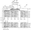
도 8은 본 발명의 제 2 실시 예에 따른 액정 표시장치를 나타내는 도면이고, 도 9는 본 발명의 제 2 실시 예에 따른 게이트 구동회로를 나타내는 도면이다.FIG. 8 is a view showing a liquid crystal display device according to a second embodiment of the present invention, and FIG. 9 is a view showing a gate driving circuit according to a second embodiment of the present invention.
도 8 및 도 9를 참조하면, 본 발명의 제 2 실시 예에 따른 액정 표시장치는 게이트 구동회로(920a, 920b)가 액정패널(900)의 양측에 형성되는 것을 제외하고는 도 1에 도시된 본 발명의 제 1 실시 예와 동일한 구성을 갖는다. 이에 따라, 게이트 구동회로(920a, 920b)를 제외한 다른 구성에 대한 설명은 상술한 본 발명의 제 1 실시 예에 대한 설명으로 대신하기로 한다.8 and 9, a liquid crystal display device according to the second embodiment of the present invention is similar to the liquid crystal display device shown in FIG. 1 except that
게이트 구동회로(920a, 920b)는 액정패널(900)의 일측에 형성되어 상부 더미 게이트 라인(GL0) 및 우수번째 게이트 라인(GL2, GL4, GL6...)을 구동하는 제 1 게이트 구동회로(920a)와, 액정패널(900)의 타측에 형성되어 기수번째 게이트 라인(GL1, GL3, GL5...) 및 하부 더미 게이트 라인(GLn+1)을 구동하는 제 2 게이트 구동회로(920b)로 나누어진다.The
제 1 게이트 구동회로(920a)는 복수의 제 1 게이트 구동신호 전송라인(940a)을 통해 구동 집적회로(130)로부터 공급되는 승압된 제 1 및 제 3 게이트 스타트 신호(Vst1, Vst3)에 의해 구동 개시되어 제 1, 3, 5 및 제 7 게이트 클럭신호(CLK1, CLK3, CLK5, CLK7)에 대응되는 게이트 온 전압을 상부 더미 게이트 라인(GL0) 및 우수번째 게이트 라인들(GL2, GL4, GL6...)에 순차적으로 공급한다.The first
이를 위해, 제 1 게이트 구동회로(920a)는 더미 스테이지(922m)와 제 1 내지 제 j(단, j는 n/2인 자연수) 스테이지(9221 내지 922j)를 포함하여 구성된다.To this end, the first
더미 스테이지(922m)는 제 1 게이트 스타트 신호(Vst1)에 의해 구동되어 제 1 게이트 클럭신호(CLK1)에 대응되는 게이트 온 전압을 상부 더미 게이트 라인(GL0) 및 제 2 스테이지(9222)에 공급한다.The
j개의 스테이지(9221 내지 922j) 중 2k-1(단, k는 제 1 내지 j/2인 자연수)번째 스테이지(9221, 9223...)는 제 3 게이트 스타트 신호(Vst3)에 의해 구동되어 제 3 및 제 7 게이트 클럭신호(CLK3, CLK7)에 따라 클럭신호(CLK3, CLK7)에 대응되는 게이트 온 전압을 4i-2(단, i는 제 1 내지 n/4인 자연수)번째 게이트 라인(GL2, GL6...)에 순차적으로 공급한다. 이때, 2k-1번째 스테이지(9221, 9223...) 중 첫번째 스테이지인 제 1 스테이지(9221)는 제 3 게이트 스타트 신호(Vst3)에 의해 구동되어 제 3 게이트 클럭신호(CLK3)를 제 2 게이트 라인(GL2) 및 2k+1번째 스테이지(9223...)에 공급한다. 그리고, 2k-1번째 스테이지(9221, 9223...) 중 첫번째 스테이지(9221)를 제외한 나머지 2k+1번째 스테이지(9223...) 각각은 2k-1번째 스테이지(9221, 9223...)로부터의 출력신호에 의해 구동되어 해당 게이트 라인(GL6, GL10, GL14...)에 게이트 온 전압을 순차적으로 공급한다.The 2k-1 stages of the j stages 9221 to 922j (k is a natural number of 1 to j / 2) stages 9221, 9223, ... are driven by the third gate start signal Vst3, The gate-on voltage corresponding to the clock signals CLK3 and CLK7 is set to 4i-2 (where i is a natural number from 1 to n / 4) according to the seventh gate clock signals CLK3 and CLK7, , GL6 ... in sequence. At this time, the
j개의 스테이지(9221 내지 922j) 중 2k번째 스테이지(9222...)는 더미 스테이지(922m)의 출력신호에 의해 구동되어 제 5 및 제 1 게이트 클럭신호(CLK5, CLK1)에 따라 클럭신호(CLK5, CLK1)에 대응되는 게이트 온 전압을 4i번째 게이트 라인(GL4, GL8, GL10...)에 순차적으로 공급한다. 이때, 2k번째 스테이지(9222...) 중 첫번째 스테이지인 제 2 스테이지(9222)는 더미 스테이지(922m)의 출력신호에 의해 구동되어 제 5 게이트 클럭신호(CLK5)를 제 4 게이트 라인(GL4) 및 2k+2번째 스테이지(미도시)에 공급한다. 그리고, 2k번째 스테이지(9222...) 중 첫번째 스테이지(9222)를 제외한 나머지 2k+2번째 스테이지(미도시) 각각은 2k번째 스테이지(9222...)로부터의 출력신호에 의해 구동되어 해당 게이트 라인(GL8, GL12, GL16...)에 게이트 온 전압을 순차적으로 공급한다.The 2k-
제 2 게이트 구동회로(920b)는 복수의 제 2 게이트 구동신호 전송라인(940b)을 통해 구동 집적회로(130)로부터 공급되는 승압된 제 2 및 제 4 게이트 스타트 신호(Vst2, Vst4)에 의해 구동 개시되어 제 2, 4, 6 및 제 8 게이트 클럭신호(CLK2, CLK4, CLK6, CLK8)에 대응되는 게이트 온 전압을 기수번째 게이트 라인들(GL1, GL3, GL7...) 및 하부 더미 게이트 라인(GLn+1)에 순차적으로 공급한다.The second
이를 위해, 제 2 게이트 구동회로(920b)는 제 1 내지 제 j(단, j는 n/2인 자연수) 스테이지(9241 내지 924j)와 더미 스테이지(924m)를 포함하여 구성된다.To this end, the second
j개의 스테이지(9241 내지 924j) 중 2k-1(단, k는 제 1 내지 j/2인 자연수)번째 스테이지(9241, 9243...)는 제 2 게이트 스타트 신호(Vst2)에 의해 구동되어 제 2 및 제 6 게이트 클럭신호(CLK2, CLK6)에 따라 클럭신호(CLK2, CLK6)에 대응되는 게이트 온 전압을 4i-3(단, i는 제 1 내지 n/4인 자연수)번째 게이트 라인(GL1, GL5...)에 순차적으로 공급한다. 이때, 2k-1번째 스테이지(9241, 9243...) 중 첫번째 스테이지인 제 1 스테이지(9241)는 제 2 게이트 스타트 신호(Vst2)에 의해 구동되어 제 2 게이트 클럭신호(CLK2)를 제 1 게이트 라인(GL1) 및 2k+1번째 스테이지(9243...)에 공급한다. 그리고, 2k-1번째 스테이지(9241, 9243...) 중 첫번째 스테이지(9241)를 제외한 나머지 2k+1번째 스테이지(9243...) 각각은 2k-1번째 스테이지(9241, 9243...)로부터의 출력신호에 의해 구동되어 해당 게이트 라인(GL5, GL9, GL13...)에 게이트 온 전압을 순차적으로 공급한다.The 2k-1 stages of the j stages 9241 to 924j (where k is a natural number of 1 to j / 2) stages 9241, 9243, ... are driven by the second gate start signal Vst2, The gate-on voltage corresponding to the clock signals CLK2 and CLK6 is set to 4i-3 (where i is a natural number from 1 to n / 4) according to the first to sixth gate clock signals CLK2 and CLK6, , GL5, ..., in sequence. At this time, the
j개의 스테이지(9241 내지 924j) 중 2k번째 스테이지(9242, 9244...)는 제 4 게이트 스타트 신호(Vst4)에 의해 구동되어 제 4 및 제 8 게이트 클럭신호(CLK4, CLK8)에 따라 클럭신호(CLK4, CLK8)에 대응되는 게이트 온 전압을 4i-1번째 게이트 라인(GL3, GL7, GL11...)에 순차적으로 공급한다. 이때, 2k번째 스테이지(9242, 9244...) 중 첫번째 스테이지인 제 2 스테이지(9242)는 제 4 게이트 스타트 신호(Vst4)에 의해 구동되어 제 4 게이트 클럭신호(CLK4)를 제 3 게이트 라인(GL3) 및 2k+2번째 스테이지(9244...)에 공급한다. 그리고, 2k번째 스테이지(9242, 9244...) 중 첫번째 스테이지(9242)를 제외한 나머지 2k+2번째 스테이지(9244...) 각각은 2k번째 스테이지(9242, 9244...)로부터의 출력신호에 의해 구동되어 해당 게이트 라인(GL7, GL11, GL15...)에 게이트 온 전압을 순차적으로 공급한다.The 2k-
더미 스테이지(924m)는 제 j-1 스테이지(924j-1)의 출력신호에 의해 구동되어 제 2 게이트 클럭신호(CLK2)에 대응되는 게이트 온 전압을 하부 더미 게이트 라인(GLn+1)에 공급한다.The
이와 같은, 본 발명의 제 2 실시 예에 따른 액정 표시장치는 본 발명의 제 1 실시 예와 동일한 효과를 제공할 수 있으며, 게이트 구동회로(920a, 920b)를 액정패널(900)의 양측에 형성하여 기판의 공간 활용 및 게이트 구동회로의 형성을 용이하게 할 수 있다.The liquid crystal display device according to the second embodiment of the present invention can provide the same effects as those of the first embodiment of the present invention. The
한편, 이상에서 설명한 본 발명은 상술한 실시 예 및 첨부된 도면에 한정되는 것이 아니고, 본 발명의 기술적 사상을 벗어나지 않는 범위 내에서 여러 가지 치환, 변형 및 변경이 가능하다는 것이 본 발명이 속하는 기술분야에서 종래의 지식을 가진 자에게 있어 명백할 것이다.While the present invention has been described in connection with what is presently considered to be the most practical and preferred embodiment, it is to be understood that the invention is not limited to the disclosed embodiments, but, on the contrary, is intended to cover various modifications and equivalent arrangements included within the spirit and scope of the appended claims. Will be apparent to those of ordinary skill in the art.
상기와 같은 본 발명의 실시 예에 따른 액정 표시장치 및 그의 구동방법은 아래와 같은 효과를 제공한다.The liquid crystal display device and the driving method thereof according to the embodiment of the present invention provide the following effects.
첫째, 하나의 구동 집적회로로 액정패널을 구동함과 아울러 구동 집적회로를 액정패널에 내장함으로써 단가를 저감할 수 있으며 액정 표시장치의 두께를 최소화할 수 있다.First, by driving a liquid crystal panel with one driving integrated circuit and incorporating a driving integrated circuit into a liquid crystal panel, the unit cost can be reduced and the thickness of the liquid crystal display device can be minimized.
둘째, 각 화소셀이 수평 방향으로 배치됨으로써 데이터 라인들의 수를 1/3로 저감함으로써 소형뿐만 아니라 중형 액정 표시장치에도 적용될 수 있다.Second, by arranging each pixel cell in the horizontal direction, the number of data lines is reduced to 1/3, so that the present invention can be applied not only to a small size but also to a medium type liquid crystal display device.
셋째, 상부 및 하부 더미 게이트 라인을 이용하여 첫번째 수평구간 이전 및 마지막 수평구간 이후에 각 데이터 라인을 더미전압으로 예비충전함으로써 화상신호의 극성반전에 따른 첫번째 또는/및 수평라인에 접속된 각 화소셀의 충전 특성을 향상시킬 수 있다.Third, by precharging each data line before and after the first horizontal interval with the dummy voltage using the upper and lower dummy gate lines, each pixel cell connected to the first and / or the horizontal line according to the polarity inversion of the image signal Can be improved.
넷째, 각 게이트 라인에 공급되는 게이트 온 전압을 적어도 2 서브구간 단위로 중첩시켜 적어도 2 서브구간 동안 동일한 극성의 화상신호로 각 화소셀을 예비충전시킴으로써 고해상도 모델에서의 충전시간을 충분히 확보하여 충전불량으로 인한 화질저하를 방지할 수 있다.Fourth, by superimposing the gate-on voltage supplied to each gate line in units of at least two sub-sections and precharging each pixel cell with an image signal of the same polarity for at least two sub-periods, the charging time in the high- It is possible to prevent a deterioration of image quality due to the influence of the light.
다섯째, 게이트 구동회로를 액정패널의 양측에 형성하여 기판의 공간 활용 및 게이트 구동회로의 형성을 용이하게 할 수 있다.Fifth, a gate driving circuit may be formed on both sides of the liquid crystal panel to facilitate the space utilization of the substrate and the formation of the gate driving circuit.
Claims (12)
Translated fromKoreanPriority Applications (1)
| Application Number | Priority Date | Filing Date | Title |
|---|---|---|---|
| KR1020070057128AKR101394925B1 (en) | 2007-06-12 | 2007-06-12 | Liquid crystal display device and driving method thereof |
Applications Claiming Priority (1)
| Application Number | Priority Date | Filing Date | Title |
|---|---|---|---|
| KR1020070057128AKR101394925B1 (en) | 2007-06-12 | 2007-06-12 | Liquid crystal display device and driving method thereof |
Publications (2)
| Publication Number | Publication Date |
|---|---|
| KR20080109159A KR20080109159A (en) | 2008-12-17 |
| KR101394925B1true KR101394925B1 (en) | 2014-05-14 |
Family
ID=40368506
Family Applications (1)
| Application Number | Title | Priority Date | Filing Date |
|---|---|---|---|
| KR1020070057128AActiveKR101394925B1 (en) | 2007-06-12 | 2007-06-12 | Liquid crystal display device and driving method thereof |
Country Status (1)
| Country | Link |
|---|---|
| KR (1) | KR101394925B1 (en) |
Cited By (1)
| Publication number | Priority date | Publication date | Assignee | Title |
|---|---|---|---|---|
| US20220415232A1 (en)* | 2020-06-30 | 2022-12-29 | Hefei Boe Display Technology Co., Ltd. | Driving method and driving circuit of display panel, and display apparatus |
Families Citing this family (7)
| Publication number | Priority date | Publication date | Assignee | Title |
|---|---|---|---|---|
| KR102050511B1 (en) | 2012-07-24 | 2019-12-02 | 삼성디스플레이 주식회사 | Display device |
| KR102027170B1 (en)* | 2012-12-18 | 2019-10-01 | 엘지디스플레이 주식회사 | Liquid crystal display device and driving method thereof |
| CN103021369A (en)* | 2012-12-21 | 2013-04-03 | 北京京东方光电科技有限公司 | Method for driving liquid crystal display |
| KR102168822B1 (en)* | 2014-11-20 | 2020-10-22 | 엘지디스플레이 주식회사 | Display Device |
| CN104900180B (en)* | 2015-07-01 | 2018-02-13 | 京东方科技集团股份有限公司 | A kind of source electrode drive circuit and its driving method, display device |
| KR20170007610A (en) | 2015-07-09 | 2017-01-19 | 삼성디스플레이 주식회사 | Display device |
| DE112016004055B4 (en)* | 2015-09-08 | 2024-02-08 | Semiconductor Energy Laboratory Co., Ltd. | DISPLAY DEVICES AND ELECTRONIC DEVICE |
Citations (4)
| Publication number | Priority date | Publication date | Assignee | Title |
|---|---|---|---|---|
| KR100228282B1 (en) | 1996-09-17 | 1999-11-01 | 윤종용 | Liquid crystal display |
| KR100268557B1 (en) | 1997-02-13 | 2000-10-16 | 아베 아키라 | Method of driving a display device |
| JP2002189203A (en) | 2000-09-18 | 2002-07-05 | Lg Philips Lcd Co Ltd | Driving method and driving circuit for liquid crystal display device |
| KR20060053343A (en)* | 2004-11-15 | 2006-05-22 | 삼성에스디아이 주식회사 | Driving Method of Liquid Crystal Display |
- 2007
- 2007-06-12KRKR1020070057128Apatent/KR101394925B1/enactiveActive
Patent Citations (4)
| Publication number | Priority date | Publication date | Assignee | Title |
|---|---|---|---|---|
| KR100228282B1 (en) | 1996-09-17 | 1999-11-01 | 윤종용 | Liquid crystal display |
| KR100268557B1 (en) | 1997-02-13 | 2000-10-16 | 아베 아키라 | Method of driving a display device |
| JP2002189203A (en) | 2000-09-18 | 2002-07-05 | Lg Philips Lcd Co Ltd | Driving method and driving circuit for liquid crystal display device |
| KR20060053343A (en)* | 2004-11-15 | 2006-05-22 | 삼성에스디아이 주식회사 | Driving Method of Liquid Crystal Display |
Cited By (1)
| Publication number | Priority date | Publication date | Assignee | Title |
|---|---|---|---|---|
| US20220415232A1 (en)* | 2020-06-30 | 2022-12-29 | Hefei Boe Display Technology Co., Ltd. | Driving method and driving circuit of display panel, and display apparatus |
Also Published As
| Publication number | Publication date |
|---|---|
| KR20080109159A (en) | 2008-12-17 |
Similar Documents
| Publication | Publication Date | Title |
|---|---|---|
| US8400390B2 (en) | Gate driving device and liquid crystal display having the same | |
| KR101264719B1 (en) | Liquid crystal display device | |
| CN103714785B (en) | Liquid crystal display | |
| KR101493276B1 (en) | Timing controller, liquid crystal display comprising the same and driving method of the liquid crystal display | |
| CN102460587B (en) | Shift register, display device provided with same, and shift register driving method | |
| US8344991B2 (en) | Display device and driving method thereof | |
| JP4168339B2 (en) | Display drive device, drive control method thereof, and display device | |
| US7283603B1 (en) | Shift register with four phase clocks | |
| KR101394925B1 (en) | Liquid crystal display device and driving method thereof | |
| JP5289761B2 (en) | Liquid crystal display | |
| KR20070119346A (en) | Gate driving circuit of liquid crystal display device and driving method thereof | |
| CN101154006A (en) | LCD Monitor | |
| KR20140035756A (en) | Liquid crystal display device inculding inspection circuit and inspection method thereof | |
| KR101374103B1 (en) | Liquid crystal display device and driving method thereof | |
| KR20150005259A (en) | Display panel and display apparatus having the same | |
| KR101351379B1 (en) | Liquid crystal display device | |
| KR101407297B1 (en) | Driving device of liquid crystal display device and driving method thereof | |
| KR20080086617A (en) | LCD and its driving method | |
| KR101493219B1 (en) | Liquid crystal display device and driving method thereof | |
| JP5035165B2 (en) | Display driving device and display device | |
| KR101157941B1 (en) | Apparatus and method for driving liquid crystal display device | |
| KR20060030697A (en) | Shift register and stage circuit for liquid crystal display device for overlap driving | |
| KR101419240B1 (en) | Liquid crystal display and driving method thereof | |
| KR101340997B1 (en) | Driving circuit for liquid crystal display device and method for driving the same | |
| KR20070074176A (en) | LCD Display |
Legal Events
| Date | Code | Title | Description |
|---|---|---|---|
| PA0109 | Patent application | Patent event code:PA01091R01D Comment text:Patent Application Patent event date:20070612 | |
| PG1501 | Laying open of application | ||
| A201 | Request for examination | ||
| PA0201 | Request for examination | Patent event code:PA02012R01D Patent event date:20120531 Comment text:Request for Examination of Application Patent event code:PA02011R01I Patent event date:20070612 Comment text:Patent Application | |
| E902 | Notification of reason for refusal | ||
| PE0902 | Notice of grounds for rejection | Comment text:Notification of reason for refusal Patent event date:20131028 Patent event code:PE09021S01D | |
| E701 | Decision to grant or registration of patent right | ||
| PE0701 | Decision of registration | Patent event code:PE07011S01D Comment text:Decision to Grant Registration Patent event date:20140428 | |
| GRNT | Written decision to grant | ||
| PR0701 | Registration of establishment | Comment text:Registration of Establishment Patent event date:20140508 Patent event code:PR07011E01D | |
| PR1002 | Payment of registration fee | Payment date:20140509 End annual number:3 Start annual number:1 | |
| PG1601 | Publication of registration | ||
| FPAY | Annual fee payment | Payment date:20170413 Year of fee payment:4 | |
| PR1001 | Payment of annual fee | Payment date:20170413 Start annual number:4 End annual number:4 | |
| FPAY | Annual fee payment | Payment date:20180416 Year of fee payment:5 | |
| PR1001 | Payment of annual fee | Payment date:20180416 Start annual number:5 End annual number:5 | |
| FPAY | Annual fee payment | Payment date:20190417 Year of fee payment:6 | |
| PR1001 | Payment of annual fee | Payment date:20190417 Start annual number:6 End annual number:6 | |
| PR1001 | Payment of annual fee | Payment date:20200422 Start annual number:7 End annual number:7 | |
| PR1001 | Payment of annual fee | Payment date:20210415 Start annual number:8 End annual number:8 | |
| PR1001 | Payment of annual fee | Payment date:20230417 Start annual number:10 End annual number:10 | |
| PR1001 | Payment of annual fee | Payment date:20240415 Start annual number:11 End annual number:11 | |
| PR1001 | Payment of annual fee | Payment date:20250415 Start annual number:12 End annual number:12 |