KR101390474B1 - Apparatus for processing substrate - Google Patents
Apparatus for processing substrateDownload PDFInfo
- Publication number
- KR101390474B1 KR101390474B1KR1020130038077AKR20130038077AKR101390474B1KR 101390474 B1KR101390474 B1KR 101390474B1KR 1020130038077 AKR1020130038077 AKR 1020130038077AKR 20130038077 AKR20130038077 AKR 20130038077AKR 101390474 B1KR101390474 B1KR 101390474B1
- Authority
- KR
- South Korea
- Prior art keywords
- substrate
- boat
- space
- susceptor
- chamber
- Prior art date
- Legal status (The legal status is an assumption and is not a legal conclusion. Google has not performed a legal analysis and makes no representation as to the accuracy of the status listed.)
- Active
Links
- 239000000758substrateSubstances0.000titleclaimsabstractdescription158
- 238000012545processingMethods0.000titleclaimsabstractdescription48
- 238000000034methodMethods0.000claimsabstractdescription94
- 238000011068loading methodMethods0.000claimsabstractdescription29
- 238000003780insertionMethods0.000claimsdescription5
- 230000037431insertionEffects0.000claimsdescription5
- 230000000903blocking effectEffects0.000claimsdescription3
- 239000010408filmSubstances0.000description20
- 239000012636effectorSubstances0.000description16
- 238000010438heat treatmentMethods0.000description11
- 239000004065semiconductorSubstances0.000description9
- 238000002425crystallisationMethods0.000description4
- 230000008025crystallizationEffects0.000description4
- 238000004519manufacturing processMethods0.000description4
- 239000000463materialSubstances0.000description4
- 238000012546transferMethods0.000description4
- XUIMIQQOPSSXEZ-UHFFFAOYSA-NSiliconChemical compound[Si]XUIMIQQOPSSXEZ-UHFFFAOYSA-N0.000description3
- 230000015572biosynthetic processEffects0.000description3
- 239000006227byproductSubstances0.000description3
- 229910052710siliconInorganic materials0.000description3
- 239000010703siliconSubstances0.000description3
- 239000010409thin filmSubstances0.000description3
- 229910021417amorphous siliconInorganic materials0.000description2
- 238000000137annealingMethods0.000description2
- 239000000919ceramicSubstances0.000description2
- 238000010586diagramMethods0.000description2
- 238000005530etchingMethods0.000description2
- 239000011521glassSubstances0.000description2
- 239000002245particleSubstances0.000description2
- 238000000206photolithographyMethods0.000description2
- 238000005229chemical vapour depositionMethods0.000description1
- 238000010276constructionMethods0.000description1
- 229910021419crystalline siliconInorganic materials0.000description1
- 238000000151depositionMethods0.000description1
- 230000008021depositionEffects0.000description1
- 238000005137deposition processMethods0.000description1
- 238000009792diffusion processMethods0.000description1
- 239000002019doping agentSubstances0.000description1
- 238000009413insulationMethods0.000description1
- 239000004973liquid crystal related substanceSubstances0.000description1
- 239000002184metalSubstances0.000description1
- 238000012986modificationMethods0.000description1
- 230000004048modificationEffects0.000description1
- 229910021420polycrystalline siliconInorganic materials0.000description1
- 229920000642polymerPolymers0.000description1
- 229920005591polysiliconPolymers0.000description1
- 239000010453quartzSubstances0.000description1
- 229910052594sapphireInorganic materials0.000description1
- 239000010980sapphireSubstances0.000description1
- VYPSYNLAJGMNEJ-UHFFFAOYSA-Nsilicon dioxideInorganic materialsO=[Si]=OVYPSYNLAJGMNEJ-UHFFFAOYSA-N0.000description1
- 229910001220stainless steelInorganic materials0.000description1
- 239000010935stainless steelSubstances0.000description1
- 238000007669thermal treatmentMethods0.000description1
Images


Classifications
- H—ELECTRICITY
- H01—ELECTRIC ELEMENTS
- H01L—SEMICONDUCTOR DEVICES NOT COVERED BY CLASS H10
- H01L21/00—Processes or apparatus adapted for the manufacture or treatment of semiconductor or solid state devices or of parts thereof
- H01L21/67—Apparatus specially adapted for handling semiconductor or electric solid state devices during manufacture or treatment thereof; Apparatus specially adapted for handling wafers during manufacture or treatment of semiconductor or electric solid state devices or components ; Apparatus not specifically provided for elsewhere
- H01L21/673—Apparatus specially adapted for handling semiconductor or electric solid state devices during manufacture or treatment thereof; Apparatus specially adapted for handling wafers during manufacture or treatment of semiconductor or electric solid state devices or components ; Apparatus not specifically provided for elsewhere using specially adapted carriers or holders; Fixing the workpieces on such carriers or holders
- H01L21/67303—Vertical boat type carrier whereby the substrates are horizontally supported, e.g. comprising rod-shaped elements
- H—ELECTRICITY
- H01—ELECTRIC ELEMENTS
- H01L—SEMICONDUCTOR DEVICES NOT COVERED BY CLASS H10
- H01L21/00—Processes or apparatus adapted for the manufacture or treatment of semiconductor or solid state devices or of parts thereof
- H01L21/02—Manufacture or treatment of semiconductor devices or of parts thereof
- H01L21/04—Manufacture or treatment of semiconductor devices or of parts thereof the devices having potential barriers, e.g. a PN junction, depletion layer or carrier concentration layer
- H01L21/18—Manufacture or treatment of semiconductor devices or of parts thereof the devices having potential barriers, e.g. a PN junction, depletion layer or carrier concentration layer the devices having semiconductor bodies comprising elements of Group IV of the Periodic Table or AIIIBV compounds with or without impurities, e.g. doping materials
- H01L21/22—Diffusion of impurity materials, e.g. doping materials, electrode materials, into or out of a semiconductor body, or between semiconductor regions; Interactions between two or more impurities; Redistribution of impurities
- H01L21/225—Diffusion of impurity materials, e.g. doping materials, electrode materials, into or out of a semiconductor body, or between semiconductor regions; Interactions between two or more impurities; Redistribution of impurities using diffusion into or out of a solid from or into a solid phase, e.g. a doped oxide layer
- H—ELECTRICITY
- H01—ELECTRIC ELEMENTS
- H01L—SEMICONDUCTOR DEVICES NOT COVERED BY CLASS H10
- H01L21/00—Processes or apparatus adapted for the manufacture or treatment of semiconductor or solid state devices or of parts thereof
- H01L21/67—Apparatus specially adapted for handling semiconductor or electric solid state devices during manufacture or treatment thereof; Apparatus specially adapted for handling wafers during manufacture or treatment of semiconductor or electric solid state devices or components ; Apparatus not specifically provided for elsewhere
- H01L21/677—Apparatus specially adapted for handling semiconductor or electric solid state devices during manufacture or treatment thereof; Apparatus specially adapted for handling wafers during manufacture or treatment of semiconductor or electric solid state devices or components ; Apparatus not specifically provided for elsewhere for conveying, e.g. between different workstations
- H01L21/67739—Apparatus specially adapted for handling semiconductor or electric solid state devices during manufacture or treatment thereof; Apparatus specially adapted for handling wafers during manufacture or treatment of semiconductor or electric solid state devices or components ; Apparatus not specifically provided for elsewhere for conveying, e.g. between different workstations into and out of processing chamber
- H01L21/67757—Apparatus specially adapted for handling semiconductor or electric solid state devices during manufacture or treatment thereof; Apparatus specially adapted for handling wafers during manufacture or treatment of semiconductor or electric solid state devices or components ; Apparatus not specifically provided for elsewhere for conveying, e.g. between different workstations into and out of processing chamber vertical transfer of a batch of workpieces
- H—ELECTRICITY
- H01—ELECTRIC ELEMENTS
- H01L—SEMICONDUCTOR DEVICES NOT COVERED BY CLASS H10
- H01L21/00—Processes or apparatus adapted for the manufacture or treatment of semiconductor or solid state devices or of parts thereof
- H01L21/67—Apparatus specially adapted for handling semiconductor or electric solid state devices during manufacture or treatment thereof; Apparatus specially adapted for handling wafers during manufacture or treatment of semiconductor or electric solid state devices or components ; Apparatus not specifically provided for elsewhere
- H01L21/677—Apparatus specially adapted for handling semiconductor or electric solid state devices during manufacture or treatment thereof; Apparatus specially adapted for handling wafers during manufacture or treatment of semiconductor or electric solid state devices or components ; Apparatus not specifically provided for elsewhere for conveying, e.g. between different workstations
- H01L21/67763—Apparatus specially adapted for handling semiconductor or electric solid state devices during manufacture or treatment thereof; Apparatus specially adapted for handling wafers during manufacture or treatment of semiconductor or electric solid state devices or components ; Apparatus not specifically provided for elsewhere for conveying, e.g. between different workstations the wafers being stored in a carrier, involving loading and unloading
- H01L21/67769—Storage means
- H—ELECTRICITY
- H01—ELECTRIC ELEMENTS
- H01L—SEMICONDUCTOR DEVICES NOT COVERED BY CLASS H10
- H01L21/00—Processes or apparatus adapted for the manufacture or treatment of semiconductor or solid state devices or of parts thereof
- H01L21/67—Apparatus specially adapted for handling semiconductor or electric solid state devices during manufacture or treatment thereof; Apparatus specially adapted for handling wafers during manufacture or treatment of semiconductor or electric solid state devices or components ; Apparatus not specifically provided for elsewhere
- H01L21/677—Apparatus specially adapted for handling semiconductor or electric solid state devices during manufacture or treatment thereof; Apparatus specially adapted for handling wafers during manufacture or treatment of semiconductor or electric solid state devices or components ; Apparatus not specifically provided for elsewhere for conveying, e.g. between different workstations
- H01L21/67763—Apparatus specially adapted for handling semiconductor or electric solid state devices during manufacture or treatment thereof; Apparatus specially adapted for handling wafers during manufacture or treatment of semiconductor or electric solid state devices or components ; Apparatus not specifically provided for elsewhere for conveying, e.g. between different workstations the wafers being stored in a carrier, involving loading and unloading
- H01L21/67778—Apparatus specially adapted for handling semiconductor or electric solid state devices during manufacture or treatment thereof; Apparatus specially adapted for handling wafers during manufacture or treatment of semiconductor or electric solid state devices or components ; Apparatus not specifically provided for elsewhere for conveying, e.g. between different workstations the wafers being stored in a carrier, involving loading and unloading involving loading and unloading of wafers
- H—ELECTRICITY
- H01—ELECTRIC ELEMENTS
- H01L—SEMICONDUCTOR DEVICES NOT COVERED BY CLASS H10
- H01L21/00—Processes or apparatus adapted for the manufacture or treatment of semiconductor or solid state devices or of parts thereof
- H01L21/67—Apparatus specially adapted for handling semiconductor or electric solid state devices during manufacture or treatment thereof; Apparatus specially adapted for handling wafers during manufacture or treatment of semiconductor or electric solid state devices or components ; Apparatus not specifically provided for elsewhere
- H01L21/683—Apparatus specially adapted for handling semiconductor or electric solid state devices during manufacture or treatment thereof; Apparatus specially adapted for handling wafers during manufacture or treatment of semiconductor or electric solid state devices or components ; Apparatus not specifically provided for elsewhere for supporting or gripping
- H01L21/687—Apparatus specially adapted for handling semiconductor or electric solid state devices during manufacture or treatment thereof; Apparatus specially adapted for handling wafers during manufacture or treatment of semiconductor or electric solid state devices or components ; Apparatus not specifically provided for elsewhere for supporting or gripping using mechanical means, e.g. chucks, clamps or pinches
- H01L21/68714—Apparatus specially adapted for handling semiconductor or electric solid state devices during manufacture or treatment thereof; Apparatus specially adapted for handling wafers during manufacture or treatment of semiconductor or electric solid state devices or components ; Apparatus not specifically provided for elsewhere for supporting or gripping using mechanical means, e.g. chucks, clamps or pinches the wafers being placed on a susceptor, stage or support
Landscapes
- Engineering & Computer Science (AREA)
- Physics & Mathematics (AREA)
- Condensed Matter Physics & Semiconductors (AREA)
- General Physics & Mathematics (AREA)
- Manufacturing & Machinery (AREA)
- Computer Hardware Design (AREA)
- Microelectronics & Electronic Packaging (AREA)
- Power Engineering (AREA)
- Container, Conveyance, Adherence, Positioning, Of Wafer (AREA)
- Chemical Vapour Deposition (AREA)
- Drying Of Semiconductors (AREA)
- Recrystallisation Techniques (AREA)
Abstract
Translated fromKoreanDescription
Translated fromKorean본 발명은 기판처리장치에 관한 것으로, 더욱 상세하게는 배치타입 기판처리장치의 기판 후면에 공정 가스로 인하여 공정막이 형성되는 것을 방지하는 기판처리장치에 관한 것이다.The present invention relates to a substrate processing apparatus, and more particularly, to a substrate processing apparatus for preventing a process film from being formed due to a process gas on the rear surface of a substrate of a batch type substrate processing apparatus.
반도체, 평판 디스플레이 및 태양전지 제조에 사용되는 기판처리장치(열처리장치)는 실리콘 웨이퍼나 글래스와 같은 기판 상에 증착되어 있는 소정의 박막에 대하여 결정화, 상 변화 등의 공정을 위하여 필수적인 열처리 단계를 담당하는 장치이다. 대표적인 어닐링 장치로는 액정 디스플레이 또는 박막형 결정질 실리콘 태양전지를 제조하는 경우 기판 상에 증착된 비정질 실리콘을 폴리 실리콘으로 결정화시키는 실리콘 결정화 장치가 있다.
A substrate processing apparatus (heat treatment apparatus) used for manufacturing semiconductors, flat panel displays, and solar cells performs a thermal treatment step necessary for crystallization, phase change, and the like on a predetermined thin film deposited on a substrate such as a silicon wafer or glass . A typical annealing apparatus is a silicon crystallization apparatus for crystallizing amorphous silicon deposited on a substrate into polysilicon when a liquid crystal display or a thin film crystalline silicon solar cell is manufactured.
이와 같은 결정화 공정(열처리 공정)을 수행하기 위해서는 소정의 박막이 형성되어 있는 기판의 히팅이 가능한 열처리 장치가 있어야 한다. 예를 들어, 비정질 실리콘의 결정화를 위해서는 최소한 550도 내지 600도의 온도가 필요하다. 여기서 열처리라 함은, 작업물 또는 기판을 원하는 온도, 즉 전형적으로는 약 350 ~ 1300도 범위의 온도로 가열하는 프로세스를 의미한다. 반도체 기판의 열처리는, 예를 들면, 가열처리, 어닐링, 도펀트 물질의 확산 또는 드라이빙, 화학적 증착, 즉 CVD와 같은 물질층의 증착 또는 성장, 및 기판으로부터 물질의 에칭 또는 제거를 포함할 수 있다.
In order to perform the crystallization process (heat treatment process), a heat treatment apparatus capable of heating a substrate on which a predetermined thin film is formed must be provided. For example, a temperature of at least 550 to 600 degrees is required for crystallization of amorphous silicon. By heat treatment herein is meant a process of heating a workpiece or substrate to a desired temperature, typically a temperature in the range of about 350 to 1300 degrees. The heat treatment of the semiconductor substrate may include, for example, heat treatment, annealing, diffusion or driving of the dopant material, chemical vapor deposition, i.e. deposition or growth of a layer of material such as CVD, and etching or removal of material from the substrate.
통상적으로 기판처리장치에는 하나의 기판에 대하여 열처리를 수행할 수 있는 매엽식(single wafer type)과 복수개의 기판에 대하여 열처리를 수행할 수 있는 배치식(batch type)이 있다. 매엽식은 장치의 구성이 간단한 이점이 있으나 생산성이 떨어지는 단점이 있어서 최근의 대량 생산용으로는 배치식이 각광을 받고 있다.
Typically, a substrate processing apparatus includes a single wafer type capable of performing a heat treatment on one substrate and a batch type capable of performing heat treatment on a plurality of substrates. There is a merit of simple configuration of the apparatus, but there is a disadvantage that the productivity is low, and the batch formula is getting popular for the mass production in recent years.
배치식 기판처리장치는 공정처리능력을 향상시키기 위해서 챔버 내부에 기판을 다량으로 로딩하기 위한 기판 로딩용 보트를 포함한다. 배치식 기판처리장치는 공정을 진행할 때 슬롯이 기판의 가장자리 부분을 국부적으로 거치하고 있기 때문에, 예를 들어 막형성을 하는 공정 중에 반도체 기판의 양면 및 반도체 기판의 하부를 지지하는 보트 및 슬롯들 등에도 모두 반도체 공정용 막이 형성된다.
The batch type substrate processing apparatus includes a substrate loading boat for loading a large amount of substrate into the chamber to improve process processing capability. Since the slot locally rests on the edge portion of the substrate in the process of the batch type substrate processing apparatus, for example, in the process of forming the film, All of which form a semiconductor process film.
따라서, 반도체 제조용 막 공정이 완료된 후 기판을 언로딩할 경우, 기판과 슬롯에 일체로 연결된 막이 파쇄되며, 파쇄시 파티클이 발생하고 기판의 뒷면은 기계적 스트레스가 점점 더해져 반도체 기판이 휘는 현상이 발생한다. 뿐만 아니라, 반도체 기판 후면의 막 균일성은 앞면의 막 균일성에 비해 현저히 감소하기 때문에 후속공정, 특히 사진공정(photolithography)에 많은 공정문제를 야기한다.Therefore, when the substrate is unloaded after the film forming process for semiconductor manufacturing is completed, the film integrally connected to the substrate and the slot is broken, particles are generated at the time of disintegration, mechanical stress is increasingly applied to the back surface of the substrate, . In addition, film uniformity on the backside of the semiconductor substrate is significantly reduced compared to film uniformity on the front side, resulting in many process problems in subsequent processes, particularly photolithography.
본 발명의 목적은 기판의 뒷면에 공정막이 형성되는 것을 방지하는 데 있다.An object of the present invention is to prevent formation of a process film on the back surface of a substrate.
본 발명의 다른 목적들은 다음의 상세한 설명과 첨부한 도면으로부터 보다 명확해질 것이다.Other objects of the present invention will become more apparent from the following detailed description and the accompanying drawings.
본 발명의 일 실시예에 의하면, 기판처리장치는 기판이 적재되는 적재공간 및 상기 기판에 대한 공정이 이루어지는 공정공간을 제공하는 챔버; 상하방향을 따라 기립 배치된 하나 이상의 보트프레임을 구비하며, 승강을 통해 상기 적재공간 및 상기 공정공간으로 이동가능한 보트; 상기 보트프레임 상에 설치되어 상기 보트프레임의 길이방향을 따라 이격배치되며, 상기 보트가 상기 공정공간으로 이동함에 따라 상기 기판이 상부면에 순차적으로 놓여지는 복수의 서셉터들; 상기 보트프레임과 나란하게 배치되는 수직로드 및 상기 수직로드의 내측면으로부터 돌출되어 상기 기판을 지지하는 기판지지팁을 구비하며, 상기 수직로드는 상기 보트가 상기 공정공간으로 이동시 상기 보트프레임의 길이방향을 따라 상대적으로 이동하는 하나 이상의 홀더를 포함한다.According to an embodiment of the present invention, a substrate processing apparatus includes a chamber for providing a loading space in which a substrate is loaded and a processing space in which a process for the substrate is performed; A boat having at least one boat frame standing upright along the vertical direction, and capable of being moved to the loading space and the process space through an elevation; A plurality of susceptors installed on the boat frame and spaced apart from each other along the longitudinal direction of the boat frame and sequentially placed on the upper surface of the boat as the boat moves into the process space; A vertical rod disposed parallel to the boat frame and a substrate support tip protruding from an inner surface of the vertical rod to support the substrate, Lt; RTI ID = 0.0 > and / or < / RTI >
상기 챔버는 상기 적재공간과 상기 공정공간 사이에 형성된 연결공간을 가지며, 상기 기판처리장치는 상기 연결공간 상에 배치되어 상기 적재공간과 상기 공정공간을 차단하며, 상기 수직로드의 상단에 연결되어 상기 보트가 상기 적재공간으로부터 상기 공정공간으로 이동시 상기 보트와 함께 상기 공정공간으로 이동하는 그립플레이트를 더 포함할 수 있다.Wherein the chamber has a connection space formed between the loading space and the process space and the substrate processing apparatus is disposed on the connection space to block the loading space and the process space, And a grip plate on which a boat moves from the loading space to the processing space with the boat when the boat moves from the loading space to the processing space.
상기 챔버는, 상부가 개방되며, 일측에 형성되어 상기 기판이 출입하는 통로 및 상기 적재공간을 가지는 하부챔버; 및 상기 하부챔버의 상부에 설치되어 상기 하부챔버의 개방된 상부와 연통되는 개방된 하부를 가지며, 상기 공정공간을 제공하는 상부챔버를 구비할 수 있다.The chamber may include a lower chamber having an upper opening and a passage formed on one side of the substrate and having the loading space therein; And an upper chamber provided at an upper portion of the lower chamber and having an opened lower portion communicating with an open upper portion of the lower chamber, the upper chamber providing the processing space.
상기 기판처리장치는 상기 연결공간에 설치되며, 내부면으로부터 돌출되어 상부에 놓여진 상기 그립플레이트를 지지하는 지지돌기를 가지는 지지링을 더 포함할 수 있다.The substrate processing apparatus may further include a support ring installed in the connection space and having a support protrusion protruding from the inner surface to support the grip plate.
상기 홀더는 상기 보트가 상기 공정공간으로 이동시 상기 서셉터에 형성된 삽입홀을 통해 상대적으로 이동할 수 있다.The holder can relatively move through the insertion hole formed in the susceptor when the boat moves to the process space.
상기 서셉터는 상부면으로부터 함몰되어 상기 기판과 대응되는 형상을 가지며, 상기 기판이 놓여지는 안착홈을 가질 수 있다.The susceptor is recessed from the upper surface and has a shape corresponding to the substrate, and may have a seating groove on which the substrate is placed.
상기 기판처리장치는, 상기 보트프레임의 상부에 연결되며, 상기 보트가 상기 공정공간으로 이동시 상기 그립플레이트를 들어올리는 상부차단플레이트를 더 포함할 수 있다.The substrate processing apparatus may further include an upper shutoff plate connected to an upper portion of the boat frame and lifting the grip plate when the boat moves to the process space.
상기 상부차단플레이트는 상기 홀더와 대응되는 위치에 형성된 관통홀을 가지며, 상기 홀더는 상기 보트가 상기 공정공간으로 이동시 상기 관통홀을 통해 이동가능할 수 있다.The upper blocking plate may have a through hole formed at a position corresponding to the holder, and the holder may be movable through the through hole when the boat moves to the process space.
상기 보트프레임은 내측면으로부터 돌출되어 상기 서셉터를 지지하며, 상기 보트프레임의 길이방향을 따라 이격배치되는 서셉터지지팁을 구비할 수 있다.The boat frame may include a susceptor support tip projecting from an inner surface thereof to support the susceptor and spaced apart along the longitudinal direction of the boat frame.
본 발명의 일 실시예에 의하면, 기판을 서셉터에 로딩함에 따라 기판의 뒷면에 공정막이 형성되는 것을 방지할 수 있다. 따라서, 기판의 수율을 향상시키고 기판의 생산성을 증대할 수 있다.According to an embodiment of the present invention, the substrate can be prevented from being formed on the back surface of the substrate by loading the substrate on the susceptor. Therefore, the yield of the substrate can be improved and the productivity of the substrate can be increased.
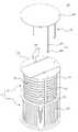
도 1은 본 발명의 일 실시예에 따른 기판처리장치를 개략적으로 나타내는 도면이다.
도 2는 도 1에 도시한 보트가 공정위치로 전환된 상태를 나타내는 도면이다.
도 3은 도 1에 도시한 보트유닛을 나타내는 사시도이다.
도 4는 도 3에 도시한 서셉터를 나타내는 도면이다.
도 5 내지 도 8은 기판이 서셉터에 로딩되는 과정을 나타내는 도면이다.
도 9 내지 도 11은 보트유닛이 공정위치로 전환되는 과정을 나타내는 도면이다.1 is a schematic view of a substrate processing apparatus according to an embodiment of the present invention.
Fig. 2 is a view showing a state where the boat shown in Fig. 1 is switched to a process position. Fig.
3 is a perspective view showing the boat unit shown in Fig.
4 is a view showing the susceptor shown in Fig.
5 to 8 are views showing a process of loading a substrate into a susceptor.
9 to 11 are diagrams showing a process in which the boat unit is switched to the process position.
이하, 본 발명의 바람직한 실시예들을 첨부된 도 1 내지 도 11을 참고하여 더욱 상세히 설명한다. 본 발명의 실시예들은 여러 가지 형태로 변형될 수 있으며, 본 발명의 범위가 아래에서 설명하는 실시예들에 한정되는 것으로 해석되어서는 안 된다. 본 실시예들은 당해 발명이 속하는 기술분야에서 통상의 지식을 가진 자에게 본 발명을 더욱 상세하게 설명하기 위해서 제공되는 것이다. 따라서 도면에 나타난 각 요소의 형상은 보다 분명한 설명을 강조하기 위하여 과장될 수 있다.
Hereinafter, preferred embodiments of the present invention will be described in detail with reference to the accompanying drawings. The embodiments of the present invention can be modified in various forms, and the scope of the present invention should not be construed as being limited to the embodiments described below. The embodiments are provided to explain the present invention to a person having ordinary skill in the art to which the present invention belongs. Accordingly, the shape of each element shown in the drawings may be exaggerated to emphasize a clearer description.
또한, 실시예에서 설명하는 기판(W) 외에 다양한 피처리체에도 응용될 수 있음은 당업자로서 당연하다. 예를 들어, 본 발명에서 처리될 수 있는 기판의 종류는 특별하게 제한되지 아니한다. 따라서, 반도체 공정 전반에서 일반적으로 이용되는 글래스, 플라스틱, 폴리머, 실리콘 웨이퍼, 스테인레스 스틸, 사파이어 등 다양한 재질의 기판이 본 발명의 기판처리장치에서 처리될 수 있다. 또한, 본 발명에서 기판을 처리한다 함은 기판 그 자체뿐만 아니라 기판 상에 형성된 소정의 막 또는 패턴 등을 처리하는 경우를 포함하는 것으로 이해될 수 있다.
It is obvious to those skilled in the art that the present invention can be applied to various substrates other than the substrate W described in the embodiments. For example, the type of substrate that can be processed in the present invention is not particularly limited. Therefore, substrates of various materials such as glass, plastic, polymer, silicon wafer, stainless steel, and sapphire generally used throughout the semiconductor processing can be processed in the substrate processing apparatus of the present invention. In addition, the processing of the substrate in the present invention can be understood to include not only the substrate itself, but also a case where a predetermined film or pattern formed on the substrate is processed.
또한, 본 발명의 기판처리장치의 용도 또한 특별히 제한되지 아니한다. 따라서 본 발명의 기판처리장치를 이용하여 전반적인 반도체공정, 예를 들어, 증착공정, 식각공정, 표면개질공정 등이 수행될 수 있다. 뿐만 아니라, 이하에서는 발명의 주요한 구성요소에 대해서만 설명하며, 이용되는 목적에 따라 다양한 구성요소들이 본 발명의 기판처리장치에 추가적으로 포함할 수 있음은 자명하다.
The use of the substrate processing apparatus of the present invention is also not particularly limited. Therefore, an overall semiconductor process such as a deposition process, an etching process, a surface modification process, and the like can be performed using the substrate processing apparatus of the present invention. In addition, only the major components of the present invention will be described below, and it is apparent that various components may be additionally included in the substrate processing apparatus of the present invention depending on the purpose of use.
도 1은 본 발명의 일 실시예에 따른 기판처리장치를 개략적으로 나타내는 도면이며, 도 2는 도 1에 도시한 보트가 공정위치로 전환된 상태를 나타내는 도면이다. 도 1 및 도 2에 도시한 바와 같이, 기판처리장치(100)는 상부가 개방된 형상을 가지는 하부챔버(20) 및 하부챔버(20)의 개방된 상부를 폐쇄하며 기판(W)에 대한 공정이 이루어지는 공정공간(12)을 제공하는 공정챔버(10)를 포함한다. 지지링(30)은 공정챔버(10)의 개방된 하부 및 하부챔버(20)의 개방된 상부('연결공간')에 설치되며, 내주면으로부터 돌출된 지지돌기(35)를 가질 수 있다.
FIG. 1 is a view schematically showing a substrate processing apparatus according to an embodiment of the present invention, and FIG. 2 is a view showing a state where the boat shown in FIG. 1 is switched to a process position. 1 and 2, the
하부챔버(20)는 기판(W)이 이송하는 통로(3)를 가질 수 있으며, 기판(W)은 통로(3)를 통해 하부챔버(20)의 내부로 이송될 수 있다. 예를 들어, 하부챔버(20)의 통로(3)는 다수의 공정 챔버들에 연결되는 트랜스퍼챔버(도시안함)와 연결될 수 있으며, 기판(W)은 트랜스퍼챔버로부터 엔드이펙터(end-dffector)(도 5의 65)에 의해 하부챔버(20)의 내부로 이송될 수 있다. 게이트 밸브(4)는 통로(3)의 외측에 설치되며, 통로(3)는 게이트 밸브(4)에 의해 개방 및 폐쇄될 수 있다.
The
기판처리장치(100)의 내부에는 통로(3)를 통해 이송되는 복수의 기판(W)들이 적재되는 보트(boat)(41)가 설치된다. 보트(41)는 하부챔버(20)의 내부에 제공된 적재공간(22) 내에 위치하는 동안(또는 '적재위치'), 기판(W)은 보트(20) 내에 적재될 수 있다. 보트(20)는 기판이 적재되는 상부보트(42)와 상부보트(42)의 하부에 연결되어 상부보트(42)를 지지하는 하부보트(43)를 포함할 수 있다. 보트(41)가 공정위치로 전환된 경우, 공정챔버(20)의 개방된 하부를 통해 공정챔버(10) 내부의 열손실을 최소화하기 위해 하부보트(43) 상에는 다수의 단열플레이트(67)를 구비될 수 있다.
A
보트유닛(40)은 후술하는 바와 같이, 기판(W)이 적재되는 서셉터(55)를 구비하는 상부보트(42), 단열플레이트(67)가 구비되는 하부보트(43), 그리고 기판(W)을 서셉터(55)에 용이하게 로딩하기 위한 그립플레이트(44), 홀더(45) 및 상부 차단플레이트(50)를 포함한다. 서셉터(55)는 기판(W)들은 보트(41)의 내부방향으로 나란하게 돌출되게 형성되는 서셉터지지팁(도5의 62)(또는 슬롯) 상에 놓여지며, 후술하는 바와 같이, 보트(41)가 상승함에 따라 기판(W)은 다음 서셉터지지팁(도5의 62) 상에 놓여진 서셉터(55)에 순차적으로 상하방향으로 적재될 수 있다. 기판(W)은 서셉터(55) 상에 모두 적재되며, 보트(41)는 내부반응튜브(14)의 내부로 이동하며(또는 '공정위치'), 기판(W)에 대한 공정이 이루어질 수 있다.
The
또한, 하부보트(43)의 하부에는 베이스플레이트(69)가 설치될 수 있으며, 베이스플레이트(69)는 보트(41)와 함께 승강할 수 있다. 보트(41)가 공정위치로 전환될 경우, 베이스플레이트(69)는 공정공간(16)을 폐쇄한다. 단열플레이트(67) 및 베이스플레이트(69)는 세라믹이나 쿼츠(quartz), 또는 메탈에 세라믹을 코팅한 재질일 수 있으며, 공정진행 시 반응영역 내의 열이 적재공간(22)으로 이동하는 것을 최소화할 수 있다.
A
베이스플레이트(29)의 하부에는 모터하우징(70)이 설치된다. 회전축(72)의 일측은 하부보트(43)와 연결되며, 회전축(72)을 회전하는 회전모터(도시안함)는 모터하우징(70)의 내부에 고정설치될 수 있다. 회전모터는 보트(41)가 공정위치로 전환되어 기판(W)에 대한 공정이 이루어질 경우, 회전축(72)을 구동하여 회전축(72)과 함께 보트(41)를 회전할 수 있다.
A motor housing (70) is installed below the base plate (29). One side of the
모터하우징(70)은 브래킷(74)에 고정되며, 브래킷(74)은 하부챔버(20)에 연결된 승강로드(76)를 따라 승강한다. 브래킷(74)은 승강로드(74)에 나사체결되며, 승강로드(74)는 승강모터(77)와 연결되어 승강로드(74)의 회전에 의해 브래킷(74)은 승강할 수 있다. 즉, 승강모터(77)의 회전에 의해 승강로드(74)는 회전하며, 이로 인해 브래킷(74)과 모터하우징(70)은 함께 승강할 수 있다.
The
공정챔버(10)는 기판(W)에 대한 공정을 수행가능하도록 내부공간(12)을 가지며, 내부공간(12)에는 내부반응튜브(14)가 설치된다. 내부반응튜브(14)는 기판(W)에 대한 공정이 이루어지도록 공정공간(16)을 형성하며, 공정챔버(10)의 내부공간(12)과 공정공간(16)을 구획한다. 즉, 도 2에 도시한 바와 같이, 보트(41)가 공정공간(16) 내부로 상승하여 공정위치로 전환된 경우, 기판(W)에 대한 공정공간(16)을 최소화하여 공정을 수행할 수 있다.
The
기판처리장치(100)는 기판(W)을 가열하는 히터(도시안함)를 포함하며, 예를 들어 공정챔버(10)의 상부 또는 측벽을 따라 히터가 구비될 수 있다. 또한, 기판처리장치(100)는 공정공간(16)으로 공정가스를 공급하는 복수개의 공급노즐(82) 및 배기노즐(84)을 구비할 수 있다. 공급노즐(82)은 공정챔버(10)의 일측에 형성된 가스공급라인(80)에 연결되며, 외부로부터 공정가스를 공급받는다.
The
공급노즐(82) 및 배기노즐(84)에 각각 형성된 공급구 및 배기구(도시안함)를 통해 기판(W)을 향해 공정가스를 공급 및 배기 가능하며, 공급구 및 배기구의 높이는 서로 상이할 수 있다. 공급노즐(82) 및 공급구는 공정공간(14)에 위치하여 적층된 기판(W)에 반응가스를 공급할 수 있다. 또한, 배기노즐(84)은 공급노즐(82)의 반대편에 설치되어 공정 중 발생하는 미반응가스 및 반응부산물들을 외부로 배출할 수 있다.
The process gas can be supplied and exhausted toward the substrate W through the supply port and the exhaust port (not shown) respectively formed in the
배기노즐(84)은 제1 출력라인(85)과 연결되며, 배기노즐(84)을 통해 흡입된 미반응가스 및 반응부산물들은 제1 출력라인(85)을 통해 배출된다. 출력밸브(도시안함)는 제1 출력라인(85) 상에 설치될 수 있으며, 제1 출력라인(85)을 개폐할 수 있다. 또한, 제1 출력라인(85) 상에는 터보펌프(86)가 설치되어 미반응가스 및 반응부산물들을 강제 배출할 수 있다. 하부챔버(20) 또한, 제2 출력라인(88)이 연결되어 제2 출력라인(88)을 통해 적재공간(22)은 배기할 수 있다.
The
앞서 설명한 바와 같이, 기판처리장치(100)는 공정처리능력을 향상시키기 위해서 내부에 기판(W)을 다량으로 로딩하기 위한 보트(41)를 포함한다. 기존의 보트유닛(40)을 사용하여 기판에 대한 공정을 진행할 경우, 보트(41)의 슬롯 상에 놓여진 기판은 기판의 가장자리 부분을 국부적으로 거치하고 있다. 예를 들어 공정가스를 통해 기판상에 공정막 형성을 하는 경우, 반도체 기판의 양면 및 기판(W)의 하부를 지지하는 보트(41) 및 슬롯들 등에도 모두 공정용 막이 형성된다.
As described above, the
따라서, 반도체 제조용 막 공정이 완료된 후 기판(W)을 언로딩할 경우, 기판(W)과 슬롯에 일체로 연결된 막이 파쇄되며, 파쇄시 파티클이 발생하고 기판(W)의 뒷면은 기계적 스트레스가 점점 더해져 기판(W)이 휘는 현상이 발생한다. 뿐만 아니라, 기판(W) 후면의 막 균일성은 앞면의 막 균일성에 비해 현저히 감소하기 때문에 후속공정, 특히 사진공정(photolithography)에 많은 공정문제를 야기한다.
Therefore, when the substrate W is unloaded after the film forming process for semiconductor manufacturing is completed, the film integrally connected to the substrate W and the slot is broken, particles are generated at the time of disintegration, And the substrate W is bent. In addition, the film uniformity on the backside of the substrate W is significantly reduced compared to the film uniformity on the front side, which causes many process problems in subsequent processes, particularly photolithography.
즉, 본 발명인 기판처리장치(100)는 기판(W) 후면의 막이 형성되는 것을 방지하기 위해 기판(W)을 서셉터(55)의 상부에 로딩하여 공정가스가 기판(W)의 후면에 유입을 차단하여 기판(W) 후면에 막이 형성되는 것을 방지할 수 있다. 이어지는 도면을 통해 기판(W) 후면의 막이 형성되는 것을 방지하는 보트유닛(40)에 대해 이어지는 도면과 함께 상세히 설명하고자 한다.
That is, the
도 3은 도 1에 도시한 보트유닛을 나타내는 도면이며, 도 4는 도 3에 도시한 서셉터를 나타내는 도면이다. 도 3 및 도 4에 도시한 바와 같이, 보트유닛(40)은 상부보트(42)와 하부보트(43)를 포함한다. 상부보트(41)에는 기둥형 보트프레임(60)의 서셉터지지팁(도5의 62)에 놓여지는 서셉터(55) 및 보트프레임(60)의 상부에 연결되는 상부차단플레이트(50)가 포함될 수 있으며, 하부보트(43)에는 앞서 설명한 바와 같이, 단열플레이트(67)가 구비할 수 있다. 또한 보트유닛(40)은 그립플래이트(44) 및 홀더(45)를 더 포함하며, 이하에서 생략되는 발명의 구성 및 작동과정은 전술한 내용으로 대체될 수 있다.
Fig. 3 is a view showing the boat unit shown in Fig. 1, and Fig. 4 is a view showing the susceptor shown in Fig. 3 and 4, the
앞서 설명한 바와 같이, 지지링(30)은 공정챔버(10)의 개방된 하부 및 하부챔버(20)의 개방된 상부에 고정 설치될 수 있으며, 내주면으로부터 돌출된 지지돌기(35)를 가진다. 그립플레이트(44)는 지지돌기(35)의 상부에 배치되며, 지지돌기(35)에 의해 지지되어 적재공간(22)과 공정공간(16)을 차단할 수 있다. 홀더(45)는 그립플레이트(44)의 하면에 수직연결되며, 바람직하게는 엔드이펙터(도 5의 65)에 의해 이송된 기판(W)을 용이하게 지지하기 위해 기설정된 위치에 복수개로 배치될 수 있다.
As described above, the
홀더(45)는 그립플레이트(44)의 하면에 각각 수직연결되는 수직로드(47) 및 수직로드(47)의 하단부에 연결되어 엔드이펙터(도 5의 65)에 의해 이송된 기판(W)을 지지하는 기판지지팁(49)를 구비할 수 있다. 기판지지팁(49)는 인입된 기판(W)을 용이하게 지지하기 위해 기판(W)의 중심을 향해 돌출되는 형상을 가질 수 있다.
The
상부보트(41)는 기둥형으로 기립설치되는 복수의 보트프레임(60)들을 가진다. 보트프레임(60) 사이로 엔드이펙터(도 5의 65)를 통한 기판(W)의 인출 및 인입을 위해 전면개방부(61)가 형성된다. 전면개방부(61)는 평면상으로 이동하는 엔드이펙터(도 5의 65)의 작업경로에 대해 반원주상으로 보트프레임(60)이 배치되어 전면개방부(61)를 이루게 된다. 서셉터지지팁(도 5의 62)은 보트프레임(60)의 길이방향을 따라 이격배치되며, 서셉터(55)는 서셉터지지팁(도 5의 62)의 상부에 놓여져 지지된다.
The
서셉터(55)는 기판(W)과 대응되는 형상을 가질 수 있으며, 가장자리에는 홀더(45)가 삽입가능한 삽입홀(57)이 각각 형성될 수 있다. 또한, 서셉터(55)는 기판(W)의 뒷면이 밀착될 수 있도록 기판(W)이 놓여지는 안착홈(59)을 가지며, 기판(W)의 외주면은 안착홈(59)에 로딩된다. 따라서, 기판(W)의 뒷면은 물론 기판(W)의 외주면으로 공정가스의 유입을 차단함으로써 기판(W)의 측면 및 뒷면의 막 형성을 방지할 수 있다.
The
보트프레임(60)의 상부에는 상부 차단플레이트(50)가 연결될 수 있으며, 상부 차단플레이트(50)는 기판(W)과 대응되는 형상을 가질 수 있다. 상부 차단플레이트(50)의 단면적은 그립플레이트(44)의 단면적보다 작으며, 서셉터(55)의 단면적보다 클 수 있다. 상부 차단플레이트(50)의 내면에는 관통홀(52)이 각각 형성되며, 홀더(45)는 관통홀(52)에 삽입가능하다. 또한, 보트프레임(60)의 하부에는 하부 차단플레이트(도시안함)가 설치될 수 있으며, 하부 차단플레이트의 하부에는 하부보트(43)가 연결될 수 있다. 하부보트(43)는 상하방향을 따라 복수개의 단열플레이트(67)가 적층된 상태로 구비할 수 있다.
The
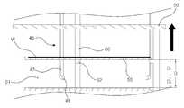
도 5 내지 도 8은 기판이 서셉터에 로딩되는 과정을 나타내는 도면이다. 앞서 설명한 바와 같이, 엔드이펙터(65)는 하부챔버(20)의 통로(3)를 통해 기판(W)을 이송한다. 엔드이펙터(65)에 놓여진 기판(W)은 하부챔버(20)를 통해 보트(41)의 전면개방부(61)로 이송된다. 상부 차단플레이트(50)와 최상단에 배치되는 서셉터(55), 그리고 최상단에 배치되는 서셉터로부터 순차적으로 적층되는 서셉터(55)들 사이의 이격공간(pitch)(D)은 엔드이펙터(65)의 작업공간을 제공하게 된다. 또한, 상부보트(41)는 보트유닛(40)의 하부에 연결된 승강유닛(도시안함)에 의해 기설정된 간격으로 승강 가능하다.
5 to 8 are views showing a process of loading a substrate into a susceptor. As described above, the
도 5에 도시한 바와 같이, 기판지지팁(49)는 보트(41)가 상승함에 따라 상부 차단플레이트(50)의 관통홀(52)을 관통하여 서셉터(55)의 상부로부터 기설정된 간격(D2) 이격된 상태로 배치된다. 상부 차단플레이트(50)와 기판지지팁(49) 사이(D1)로 엔드이펙터(65)가 인입되며, 도 6에 도시한 바와 같이, 엔드이펙터(65)가 하강함에 따라 기판(W)은 기판지지팁(49)에 안착되며, 엔드이펙터(65)는 서셉터(55)와 기판지지팁(49) 사이(D2)에 배치된다.
5, the
기판(W)이 기판지지팁(49)에 안착된 후 도 7에 도시한 바와 같이, 엔드이펙터(65)는 보트(41)의 전면개방부(61)로부터 인출된다. 엔드이펙터(65)가 보트(41)의 전면개방부(61)로부터 인출이 완료되면, 도 8에 도시한 바와 같이, 보트(41)는 기설정된 높이로 상승하여 기판(W)은 서셉터(55)의 안착홈(59) 상에 로딩된다. 기판지지팁(49)은 보트의 상승에 의해 최상단에 설치되는 서셉터(55)와 그 하부에 배치되는 서셉터(55) 사이에 기설정된 간격(D1)을 유지할 수 있으며, 도 5 내지 도 8에 도시한 과정을 순차적으로 반복하여 기판(W)은 적층된 서셉터(55) 상에 각각 로딩될 수 있다.
The
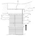
도 9 내지 도 11은 보트유닛이 공정위치로 전환되는 과정을 나타내는 도면이다. 도 9 내지 도 11에 도시한 바와 같이, 홀더(45)는 보트유닛(40)이 승강함에 따라 상부 차단플레이트(50)의 관통홀(52) 및 서셉터(55)의 삽입홀(57)을 통해 이동할 수 있다. 따라서, 홀더(45)는 엔드이펙터(65)로부터 안내된 기판(W)을 지지하며, 다시 기판(W)을 서셉터(55)에 용이하게 로딩할 수 있다. 다시 말해, 기판(W)은 엔드이펙터(65)로부터 기판지지팁(49)에 안착되며, 기판지지팁(49)로부터 서셉터(55)에 순차적으로 로딩된다.
9 to 11 are diagrams showing a process in which the boat unit is switched to the process position. 9 to 11, the
기판(W)이 상부로부터 최하단에 설치되는 서셉터(55) 상에 모두 로딩되면 상부 차단플레이트(50)와 그립플레이트(44)는 맞닿는다. 보트(41)가 상승함에 따라 상부 차단플레이트(50)는 그립플레이트(44)를 지지하여 함께 상승하며, 보트(41)는 공정위치로 전환되어 기판(W)에 대한 공정을 진행한다. 상부 차단플레이트(50)의 상부면에는 가이드홈(51)을 가질 수 있으며, 그립플레이트(44)의 하부면에는 가이드홈(51)과 대응되는 형상의 가이드돌기(도시안함)가 구비될 수 있다. 따라서, 보트(41)가 상승함에 따라 가이드돌기가 가이드홈(51)에 끼워진 상태로 안정적으로 연결되어 상승할 수 있다.
The
즉, 본 발명인 기판처리장치(100)는 서셉터(55) 상에 기판(W)을 로딩함으로써 기판의 후면에 공정가스가 유입되는 것을 방지할 수 있다. 또한, 서셉터(55) 상에 형성된 안착홈(59)에 기판(W)이 로딩된 상태로 기판(W)에 대한 공정을 진행할 경우, 기판(W)의 후면 및 측면에 공정막이 형성되는 것을 최소화할 수 있다. 뿐만 아니라, 기판(W)이 서셉터(55)에 로딩된 상태로 기판(W)에 대한 열처리를 진행할 경우, 기판의 전면이 서셉터(55)와 접촉한 상태에서 서셉터(55)를 통해 열전달이 이루어질 수 있으므로, 기판(W)의 온도 균일성을 향상시킬 수 있다. 반면, 기판(W)을 슬롯 상에 로딩할 경우, 기판(W)이 국부적으로 접촉하여 온도균일성이 저하될 수 있다. 따라서, 본 기판처리장치(100)는 기판(W)의 수율을 향상시키고 기판(W)의 생산성을 증대할 수 있다.
That is, the
본 발명을 바람직한 실시예들을 통하여 상세하게 설명하였으나, 이와 다른 형태의 실시예들도 가능하다. 그러므로, 이하에 기재된 청구항들의 기술적 사상과 범위는 바람직한 실시예들에 한정되지 않는다.Although the present invention has been described in detail by way of preferred embodiments thereof, other forms of embodiment are possible. Therefore, the technical idea and scope of the claims set forth below are not limited to the preferred embodiments.
3 : 통로4 : 게이트밸브
10 : 공정챔버12 : 내부공간
14 : 내부반응튜브16 : 공정공간
20 : 하부챔버22 : 적재공간
30 : 지지링35 : 지지돌기
40 : 보트유닛41 : 보트
42 : 상부보트43 : 하부보트
45 : 홀더47 : 수직로드
49 : 기판지지팁50 : 상부 차단플레이트
51 : 가이드홀52 : 관통홀
55 : 서셉터57 : 삽입홀
59 : 안착홈60 : 보트프레임
61 : 전면개방부65 : 엔드이펙터
67 : 단열플레이트69 : 베이스플레이트
70 : 모터하우징72 : 회전축
74 : 브래킷76 : 승강로드
77 : 승강모터80 : 가스공급라인
82 : 공급노즐84 : 배기노즐
85 : 제1 출력라인85 : 펌프
88 : 제2 출력라인100 : 기판처리장치
W : 기판3: passage 4: gate valve
10: process chamber 12: inner space
14: inner reaction tube 16: process space
20: Lower chamber 22: Loading space
30: Support ring 35: Support projection
40: boat unit 41: boat
42: upper boat 43: lower boat
45: holder 47: vertical load
49: substrate support tip 50: upper shield plate
51: Guide hole 52: Through hole
55: susceptor 57: insertion hole
59: seat groove 60: boat frame
61: front opening part 65: end effector
67: insulation plate 69: base plate
70: motor housing 72: rotating shaft
74: Bracket 76: Lift rod
77: lift motor 80: gas supply line
82: Supply nozzle 84: Exhaust nozzle
85: first output line 85: pump
88: second output line 100: substrate processing apparatus
W: substrate
Claims (9)
Translated fromKorean상하방향을 따라 기립 배치된 하나 이상의 보트프레임을 구비하며, 승강을 통해 상기 적재공간 및 상기 공정공간으로 이동가능한 보트;
상기 보트프레임 상에 설치되어 상기 보트프레임의 길이방향을 따라 이격배치되며, 상기 보트가 상기 공정공간으로 이동함에 따라 상기 기판이 상부면에 순차적으로 놓여지는 복수의 서셉터들;
상기 보트프레임과 나란하게 배치되는 수직로드 및 상기 수직로드의 내측면으로부터 돌출되어 상기 기판을 지지하는 기판지지팁을 구비하며, 상기 수직로드는 상기 보트가 상기 공정공간으로 이동시 상기 보트프레임의 길이방향을 따라 상대적으로 이동하는 하나 이상의 홀더; 및
상기 연결공간 상에 배치되어 상기 적재공간과 상기 공정공간을 차단하며, 상기 수직로드의 상단에 연결되어 상기 보트가 상기 적재공간으로부터 상기 공정공간으로 이동시 상기 보트와 함께 상기 공정공간으로 이동하는 그립플레이트를 포함하는, 기판처리장치.A chamber having a loading space in which the substrate is loaded and a processing space in which the substrate is processed, and a connection space formed between the loading space and the processing space;
A boat having at least one boat frame standing upright along the vertical direction, and capable of being moved to the loading space and the process space through an elevation;
A plurality of susceptors installed on the boat frame and spaced apart from each other along the longitudinal direction of the boat frame and sequentially placed on the upper surface of the boat as the boat moves into the process space;
A vertical rod disposed parallel to the boat frame and a substrate support tip projecting from an inner surface of the vertical rod to support the substrate, One or more holders moving relative to each other; And
A gripping plate disposed on the connection space for blocking the loading space and the process space and connected to an upper end of the vertical rod for moving the boat to the process space with the boat when the boat is moved from the loading space to the process space; And the substrate processing apparatus.
상기 챔버는,
상부가 개방되며, 일측에 형성되어 상기 기판이 출입하는 통로 및 상기 적재공간을 가지는 하부챔버; 및
상기 하부챔버의 상부에 설치되어 상기 하부챔버의 개방된 상부와 연통되는 개방된 하부를 가지며, 상기 공정공간을 제공하는 상부챔버를 구비하는, 기판처리장치.The method according to claim 1,
The chamber may comprise:
A lower chamber having an opening at an upper portion and formed at one side thereof and having a passage through which the substrate enters and exits and the loading space; And
And an upper chamber provided at an upper portion of the lower chamber and having an open lower portion communicating with an open top portion of the lower chamber, the upper chamber providing the processing space.
상기 기판처리장치는 상기 연결공간에 설치되며, 내부면으로부터 돌출되어 상부에 놓여진 상기 그립플레이트를 지지하는 지지돌기를 가지는 지지링을 더 포함하는, 기판처리장치.The method according to claim 1,
Wherein the substrate processing apparatus further comprises a support ring installed in the connection space and having a support projection projecting from the inner surface and supporting the grip plate placed on the upper side.
상기 홀더는 상기 보트가 상기 공정공간으로 이동시 상기 서셉터에 형성된 삽입홀을 통해 상대적으로 이동하는, 기판처리장치.The method according to claim 1,
Wherein the holder relatively moves through an insertion hole formed in the susceptor when the boat moves to the process space.
상기 서셉터는 상부면으로부터 함몰되어 상기 기판과 대응되는 형상을 가지며, 상기 기판이 놓여지는 안착홈을 가지는, 기판처리장치.The method according to claim 1,
Wherein the susceptor is recessed from an upper surface and has a shape corresponding to the substrate, and has a seating groove on which the substrate is placed.
상기 기판처리장치는,
상기 보트프레임의 상부에 연결되며, 상기 보트가 상기 공정공간으로 이동시 상기 그립플레이트를 들어올리는 상부차단플레이트를 더 포함하는, 기판처리장치.The method according to claim 1,
The substrate processing apparatus includes:
Further comprising an upper shield plate connected to an upper portion of the boat frame and lifting the grip plate when the boat is moved into the process space.
상기 상부차단플레이트는 상기 홀더와 대응되는 위치에 형성된 관통홀을 가지며,
상기 홀더는 상기 보트가 상기 공정공간으로 이동시 상기 관통홀을 통해 이동가능한, 기판처리장치.8. The method of claim 7,
Wherein the upper shield plate has a through hole formed at a position corresponding to the holder,
Wherein the holder is movable through the through hole when the boat moves to the process space.
상기 보트프레임은 내측면으로부터 돌출되어 상기 서셉터를 지지하며, 상기 보트프레임의 길이방향을 따라 이격배치되는 서셉터지지팁을 구비하는, 기판처리장치.The method according to claim 1,
Wherein the boat frame includes a susceptor support tip projecting from an inner surface to support the susceptor and spaced apart along a longitudinal direction of the boat frame.
Priority Applications (6)
| Application Number | Priority Date | Filing Date | Title |
|---|---|---|---|
| KR1020130038077AKR101390474B1 (en) | 2013-04-08 | 2013-04-08 | Apparatus for processing substrate |
| US14/766,299US9368380B2 (en) | 2013-04-08 | 2014-02-17 | Substrate processing device with connection space |
| JP2015561262AJP6062075B2 (en) | 2013-04-08 | 2014-02-17 | Substrate processing equipment |
| PCT/KR2014/001258WO2014168331A1 (en) | 2013-04-08 | 2014-02-17 | Substrate processing device |
| CN201480008450.3ACN104981898B (en) | 2013-04-08 | 2014-02-17 | Substrate processing equipment |
| TW103112668ATWI534900B (en) | 2013-04-08 | 2014-04-07 | Apparatus for processing substrate |
Applications Claiming Priority (1)
| Application Number | Priority Date | Filing Date | Title |
|---|---|---|---|
| KR1020130038077AKR101390474B1 (en) | 2013-04-08 | 2013-04-08 | Apparatus for processing substrate |
Publications (1)
| Publication Number | Publication Date |
|---|---|
| KR101390474B1true KR101390474B1 (en) | 2014-05-07 |
Family
ID=50892923
Family Applications (1)
| Application Number | Title | Priority Date | Filing Date |
|---|---|---|---|
| KR1020130038077AActiveKR101390474B1 (en) | 2013-04-08 | 2013-04-08 | Apparatus for processing substrate |
Country Status (6)
| Country | Link |
|---|---|
| US (1) | US9368380B2 (en) |
| JP (1) | JP6062075B2 (en) |
| KR (1) | KR101390474B1 (en) |
| CN (1) | CN104981898B (en) |
| TW (1) | TWI534900B (en) |
| WO (1) | WO2014168331A1 (en) |
Cited By (4)
| Publication number | Priority date | Publication date | Assignee | Title |
|---|---|---|---|---|
| WO2016118285A1 (en)* | 2015-01-23 | 2016-07-28 | Applied Materials, Inc. | New susceptor design to eliminate deposition valleys in the wafer |
| KR101685096B1 (en)* | 2015-11-17 | 2016-12-12 | 주식회사 유진테크 | Apparatus for processing substrate and method for processing substrate using the same |
| KR101731488B1 (en)* | 2015-10-27 | 2017-05-02 | 주식회사 유진테크 | Substrate Processing Apparatus and Assembling Method for Tube Assembly |
| KR101760316B1 (en)* | 2015-09-11 | 2017-07-21 | 주식회사 유진테크 | Substrate Processing Apparatus |
Families Citing this family (286)
| Publication number | Priority date | Publication date | Assignee | Title |
|---|---|---|---|---|
| US20130023129A1 (en) | 2011-07-20 | 2013-01-24 | Asm America, Inc. | Pressure transmitter for a semiconductor processing environment |
| KR101408084B1 (en)* | 2011-11-17 | 2014-07-04 | 주식회사 유진테크 | Apparatus for processing substrate including auxiliary gas supply port |
| KR101364701B1 (en)* | 2011-11-17 | 2014-02-20 | 주식회사 유진테크 | Apparatus for processing substrate with process gas having phase difference |
| KR20130107001A (en)* | 2012-03-21 | 2013-10-01 | 엘지이노텍 주식회사 | Apparatus for deposition |
| US10714315B2 (en) | 2012-10-12 | 2020-07-14 | Asm Ip Holdings B.V. | Semiconductor reaction chamber showerhead |
| US20160376700A1 (en) | 2013-02-01 | 2016-12-29 | Asm Ip Holding B.V. | System for treatment of deposition reactor |
| US11015245B2 (en) | 2014-03-19 | 2021-05-25 | Asm Ip Holding B.V. | Gas-phase reactor and system having exhaust plenum and components thereof |
| US10941490B2 (en) | 2014-10-07 | 2021-03-09 | Asm Ip Holding B.V. | Multiple temperature range susceptor, assembly, reactor and system including the susceptor, and methods of using the same |
| US10276355B2 (en) | 2015-03-12 | 2019-04-30 | Asm Ip Holding B.V. | Multi-zone reactor, system including the reactor, and method of using the same |
| US10458018B2 (en) | 2015-06-26 | 2019-10-29 | Asm Ip Holding B.V. | Structures including metal carbide material, devices including the structures, and methods of forming same |
| US10211308B2 (en) | 2015-10-21 | 2019-02-19 | Asm Ip Holding B.V. | NbMC layers |
| US9946028B2 (en)* | 2015-12-18 | 2018-04-17 | Finisar Corporation | Wafer assembly including a guide pin wafer |
| US11139308B2 (en) | 2015-12-29 | 2021-10-05 | Asm Ip Holding B.V. | Atomic layer deposition of III-V compounds to form V-NAND devices |
| US10529554B2 (en) | 2016-02-19 | 2020-01-07 | Asm Ip Holding B.V. | Method for forming silicon nitride film selectively on sidewalls or flat surfaces of trenches |
| US10343920B2 (en) | 2016-03-18 | 2019-07-09 | Asm Ip Holding B.V. | Aligned carbon nanotubes |
| US10367080B2 (en) | 2016-05-02 | 2019-07-30 | Asm Ip Holding B.V. | Method of forming a germanium oxynitride film |
| US11453943B2 (en) | 2016-05-25 | 2022-09-27 | Asm Ip Holding B.V. | Method for forming carbon-containing silicon/metal oxide or nitride film by ALD using silicon precursor and hydrocarbon precursor |
| US10612137B2 (en) | 2016-07-08 | 2020-04-07 | Asm Ip Holdings B.V. | Organic reactants for atomic layer deposition |
| US9859151B1 (en) | 2016-07-08 | 2018-01-02 | Asm Ip Holding B.V. | Selective film deposition method to form air gaps |
| US9812320B1 (en) | 2016-07-28 | 2017-11-07 | Asm Ip Holding B.V. | Method and apparatus for filling a gap |
| KR102532607B1 (en) | 2016-07-28 | 2023-05-15 | 에이에스엠 아이피 홀딩 비.브이. | Substrate processing apparatus and method of operating the same |
| US9887082B1 (en) | 2016-07-28 | 2018-02-06 | Asm Ip Holding B.V. | Method and apparatus for filling a gap |
| CN107871681B (en) | 2016-09-27 | 2019-10-08 | 北京北方华创微电子装备有限公司 | One kind going to gas chamber and semiconductor processing device |
| US11532757B2 (en) | 2016-10-27 | 2022-12-20 | Asm Ip Holding B.V. | Deposition of charge trapping layers |
| US10714350B2 (en) | 2016-11-01 | 2020-07-14 | ASM IP Holdings, B.V. | Methods for forming a transition metal niobium nitride film on a substrate by atomic layer deposition and related semiconductor device structures |
| KR102546317B1 (en) | 2016-11-15 | 2023-06-21 | 에이에스엠 아이피 홀딩 비.브이. | Gas supply unit and substrate processing apparatus including the same |
| KR102762543B1 (en) | 2016-12-14 | 2025-02-05 | 에이에스엠 아이피 홀딩 비.브이. | Substrate processing apparatus |
| US11447861B2 (en) | 2016-12-15 | 2022-09-20 | Asm Ip Holding B.V. | Sequential infiltration synthesis apparatus and a method of forming a patterned structure |
| US11581186B2 (en) | 2016-12-15 | 2023-02-14 | Asm Ip Holding B.V. | Sequential infiltration synthesis apparatus |
| KR102700194B1 (en) | 2016-12-19 | 2024-08-28 | 에이에스엠 아이피 홀딩 비.브이. | Substrate processing apparatus |
| US10269558B2 (en) | 2016-12-22 | 2019-04-23 | Asm Ip Holding B.V. | Method of forming a structure on a substrate |
| US11390950B2 (en) | 2017-01-10 | 2022-07-19 | Asm Ip Holding B.V. | Reactor system and method to reduce residue buildup during a film deposition process |
| US10468261B2 (en) | 2017-02-15 | 2019-11-05 | Asm Ip Holding B.V. | Methods for forming a metallic film on a substrate by cyclical deposition and related semiconductor device structures |
| KR101905822B1 (en)* | 2017-03-21 | 2018-10-08 | 주식회사 유진테크 | Apparatus for processing substrate |
| US10529563B2 (en) | 2017-03-29 | 2020-01-07 | Asm Ip Holdings B.V. | Method for forming doped metal oxide films on a substrate by cyclical deposition and related semiconductor device structures |
| US10770286B2 (en) | 2017-05-08 | 2020-09-08 | Asm Ip Holdings B.V. | Methods for selectively forming a silicon nitride film on a substrate and related semiconductor device structures |
| US12040200B2 (en) | 2017-06-20 | 2024-07-16 | Asm Ip Holding B.V. | Semiconductor processing apparatus and methods for calibrating a semiconductor processing apparatus |
| US11306395B2 (en) | 2017-06-28 | 2022-04-19 | Asm Ip Holding B.V. | Methods for depositing a transition metal nitride film on a substrate by atomic layer deposition and related deposition apparatus |
| KR20190009245A (en) | 2017-07-18 | 2019-01-28 | 에이에스엠 아이피 홀딩 비.브이. | Methods for forming a semiconductor device structure and related semiconductor device structures |
| US11018002B2 (en) | 2017-07-19 | 2021-05-25 | Asm Ip Holding B.V. | Method for selectively depositing a Group IV semiconductor and related semiconductor device structures |
| US10541333B2 (en) | 2017-07-19 | 2020-01-21 | Asm Ip Holding B.V. | Method for depositing a group IV semiconductor and related semiconductor device structures |
| US11374112B2 (en) | 2017-07-19 | 2022-06-28 | Asm Ip Holding B.V. | Method for depositing a group IV semiconductor and related semiconductor device structures |
| US10590535B2 (en)* | 2017-07-26 | 2020-03-17 | Asm Ip Holdings B.V. | Chemical treatment, deposition and/or infiltration apparatus and method for using the same |
| TWI815813B (en) | 2017-08-04 | 2023-09-21 | 荷蘭商Asm智慧財產控股公司 | Showerhead assembly for distributing a gas within a reaction chamber |
| US10692741B2 (en) | 2017-08-08 | 2020-06-23 | Asm Ip Holdings B.V. | Radiation shield |
| US10770336B2 (en) | 2017-08-08 | 2020-09-08 | Asm Ip Holding B.V. | Substrate lift mechanism and reactor including same |
| US11769682B2 (en) | 2017-08-09 | 2023-09-26 | Asm Ip Holding B.V. | Storage apparatus for storing cassettes for substrates and processing apparatus equipped therewith |
| US11139191B2 (en) | 2017-08-09 | 2021-10-05 | Asm Ip Holding B.V. | Storage apparatus for storing cassettes for substrates and processing apparatus equipped therewith |
| US11830730B2 (en) | 2017-08-29 | 2023-11-28 | Asm Ip Holding B.V. | Layer forming method and apparatus |
| KR102491945B1 (en) | 2017-08-30 | 2023-01-26 | 에이에스엠 아이피 홀딩 비.브이. | Substrate processing apparatus |
| US11056344B2 (en) | 2017-08-30 | 2021-07-06 | Asm Ip Holding B.V. | Layer forming method |
| US11295980B2 (en) | 2017-08-30 | 2022-04-05 | Asm Ip Holding B.V. | Methods for depositing a molybdenum metal film over a dielectric surface of a substrate by a cyclical deposition process and related semiconductor device structures |
| US10658205B2 (en) | 2017-09-28 | 2020-05-19 | Asm Ip Holdings B.V. | Chemical dispensing apparatus and methods for dispensing a chemical to a reaction chamber |
| US10403504B2 (en) | 2017-10-05 | 2019-09-03 | Asm Ip Holding B.V. | Method for selectively depositing a metallic film on a substrate |
| US10923344B2 (en) | 2017-10-30 | 2021-02-16 | Asm Ip Holding B.V. | Methods for forming a semiconductor structure and related semiconductor structures |
| TWI655313B (en)* | 2017-11-22 | 2019-04-01 | 台灣積體電路製造股份有限公司 | Semiconductor wafer processing system and method for processing semiconductor wafer |
| US11022879B2 (en) | 2017-11-24 | 2021-06-01 | Asm Ip Holding B.V. | Method of forming an enhanced unexposed photoresist layer |
| WO2019103613A1 (en) | 2017-11-27 | 2019-05-31 | Asm Ip Holding B.V. | A storage device for storing wafer cassettes for use with a batch furnace |
| CN111344522B (en) | 2017-11-27 | 2022-04-12 | 阿斯莫Ip控股公司 | Including clean mini-environment device |
| US10872771B2 (en) | 2018-01-16 | 2020-12-22 | Asm Ip Holding B. V. | Method for depositing a material film on a substrate within a reaction chamber by a cyclical deposition process and related device structures |
| TWI799494B (en) | 2018-01-19 | 2023-04-21 | 荷蘭商Asm 智慧財產控股公司 | Deposition method |
| KR102695659B1 (en) | 2018-01-19 | 2024-08-14 | 에이에스엠 아이피 홀딩 비.브이. | Method for depositing a gap filling layer by plasma assisted deposition |
| US11081345B2 (en) | 2018-02-06 | 2021-08-03 | Asm Ip Holding B.V. | Method of post-deposition treatment for silicon oxide film |
| US10896820B2 (en) | 2018-02-14 | 2021-01-19 | Asm Ip Holding B.V. | Method for depositing a ruthenium-containing film on a substrate by a cyclical deposition process |
| WO2019158960A1 (en) | 2018-02-14 | 2019-08-22 | Asm Ip Holding B.V. | A method for depositing a ruthenium-containing film on a substrate by a cyclical deposition process |
| US10731249B2 (en) | 2018-02-15 | 2020-08-04 | Asm Ip Holding B.V. | Method of forming a transition metal containing film on a substrate by a cyclical deposition process, a method for supplying a transition metal halide compound to a reaction chamber, and related vapor deposition apparatus |
| KR102636427B1 (en) | 2018-02-20 | 2024-02-13 | 에이에스엠 아이피 홀딩 비.브이. | Substrate processing method and apparatus |
| US10975470B2 (en) | 2018-02-23 | 2021-04-13 | Asm Ip Holding B.V. | Apparatus for detecting or monitoring for a chemical precursor in a high temperature environment |
| US11473195B2 (en) | 2018-03-01 | 2022-10-18 | Asm Ip Holding B.V. | Semiconductor processing apparatus and a method for processing a substrate |
| US11629406B2 (en) | 2018-03-09 | 2023-04-18 | Asm Ip Holding B.V. | Semiconductor processing apparatus comprising one or more pyrometers for measuring a temperature of a substrate during transfer of the substrate |
| US11114283B2 (en) | 2018-03-16 | 2021-09-07 | Asm Ip Holding B.V. | Reactor, system including the reactor, and methods of manufacturing and using same |
| KR102646467B1 (en) | 2018-03-27 | 2024-03-11 | 에이에스엠 아이피 홀딩 비.브이. | Method of forming an electrode on a substrate and a semiconductor device structure including an electrode |
| US11088002B2 (en) | 2018-03-29 | 2021-08-10 | Asm Ip Holding B.V. | Substrate rack and a substrate processing system and method |
| US11230766B2 (en) | 2018-03-29 | 2022-01-25 | Asm Ip Holding B.V. | Substrate processing apparatus and method |
| KR102600229B1 (en) | 2018-04-09 | 2023-11-10 | 에이에스엠 아이피 홀딩 비.브이. | Substrate supporting device, substrate processing apparatus including the same and substrate processing method |
| US12025484B2 (en) | 2018-05-08 | 2024-07-02 | Asm Ip Holding B.V. | Thin film forming method |
| TWI811348B (en) | 2018-05-08 | 2023-08-11 | 荷蘭商Asm 智慧財產控股公司 | Methods for depositing an oxide film on a substrate by a cyclical deposition process and related device structures |
| US12272527B2 (en) | 2018-05-09 | 2025-04-08 | Asm Ip Holding B.V. | Apparatus for use with hydrogen radicals and method of using same |
| KR102596988B1 (en) | 2018-05-28 | 2023-10-31 | 에이에스엠 아이피 홀딩 비.브이. | Method of processing a substrate and a device manufactured by the same |
| TWI840362B (en) | 2018-06-04 | 2024-05-01 | 荷蘭商Asm Ip私人控股有限公司 | Wafer handling chamber with moisture reduction |
| US11718913B2 (en) | 2018-06-04 | 2023-08-08 | Asm Ip Holding B.V. | Gas distribution system and reactor system including same |
| US11286562B2 (en) | 2018-06-08 | 2022-03-29 | Asm Ip Holding B.V. | Gas-phase chemical reactor and method of using same |
| US10797133B2 (en) | 2018-06-21 | 2020-10-06 | Asm Ip Holding B.V. | Method for depositing a phosphorus doped silicon arsenide film and related semiconductor device structures |
| KR102568797B1 (en) | 2018-06-21 | 2023-08-21 | 에이에스엠 아이피 홀딩 비.브이. | Substrate processing system |
| TWI873894B (en) | 2018-06-27 | 2025-02-21 | 荷蘭商Asm Ip私人控股有限公司 | Cyclic deposition methods for forming metal-containing material and films and structures including the metal-containing material |
| KR102854019B1 (en) | 2018-06-27 | 2025-09-02 | 에이에스엠 아이피 홀딩 비.브이. | Periodic deposition method for forming a metal-containing material and films and structures comprising the metal-containing material |
| US10612136B2 (en) | 2018-06-29 | 2020-04-07 | ASM IP Holding, B.V. | Temperature-controlled flange and reactor system including same |
| US10755922B2 (en) | 2018-07-03 | 2020-08-25 | Asm Ip Holding B.V. | Method for depositing silicon-free carbon-containing film as gap-fill layer by pulse plasma-assisted deposition |
| US10388513B1 (en) | 2018-07-03 | 2019-08-20 | Asm Ip Holding B.V. | Method for depositing silicon-free carbon-containing film as gap-fill layer by pulse plasma-assisted deposition |
| US10720353B2 (en)* | 2018-07-04 | 2020-07-21 | Murata Machinery, Ltd. | Opener apparatus |
| US11053591B2 (en) | 2018-08-06 | 2021-07-06 | Asm Ip Holding B.V. | Multi-port gas injection system and reactor system including same |
| US11430674B2 (en) | 2018-08-22 | 2022-08-30 | Asm Ip Holding B.V. | Sensor array, apparatus for dispensing a vapor phase reactant to a reaction chamber and related methods |
| KR102707956B1 (en) | 2018-09-11 | 2024-09-19 | 에이에스엠 아이피 홀딩 비.브이. | Method for deposition of a thin film |
| US11024523B2 (en) | 2018-09-11 | 2021-06-01 | Asm Ip Holding B.V. | Substrate processing apparatus and method |
| US11049751B2 (en) | 2018-09-14 | 2021-06-29 | Asm Ip Holding B.V. | Cassette supply system to store and handle cassettes and processing apparatus equipped therewith |
| CN110970344B (en) | 2018-10-01 | 2024-10-25 | Asmip控股有限公司 | Substrate holding apparatus, system comprising the same and method of using the same |
| US11232963B2 (en) | 2018-10-03 | 2022-01-25 | Asm Ip Holding B.V. | Substrate processing apparatus and method |
| KR102592699B1 (en) | 2018-10-08 | 2023-10-23 | 에이에스엠 아이피 홀딩 비.브이. | Substrate support unit and apparatuses for depositing thin film and processing the substrate including the same |
| KR102546322B1 (en) | 2018-10-19 | 2023-06-21 | 에이에스엠 아이피 홀딩 비.브이. | Substrate processing apparatus and substrate processing method |
| KR102605121B1 (en) | 2018-10-19 | 2023-11-23 | 에이에스엠 아이피 홀딩 비.브이. | Substrate processing apparatus and substrate processing method |
| USD948463S1 (en) | 2018-10-24 | 2022-04-12 | Asm Ip Holding B.V. | Susceptor for semiconductor substrate supporting apparatus |
| US12378665B2 (en) | 2018-10-26 | 2025-08-05 | Asm Ip Holding B.V. | High temperature coatings for a preclean and etch apparatus and related methods |
| US11087997B2 (en) | 2018-10-31 | 2021-08-10 | Asm Ip Holding B.V. | Substrate processing apparatus for processing substrates |
| KR102748291B1 (en) | 2018-11-02 | 2024-12-31 | 에이에스엠 아이피 홀딩 비.브이. | Substrate support unit and substrate processing apparatus including the same |
| US11572620B2 (en) | 2018-11-06 | 2023-02-07 | Asm Ip Holding B.V. | Methods for selectively depositing an amorphous silicon film on a substrate |
| US11031242B2 (en) | 2018-11-07 | 2021-06-08 | Asm Ip Holding B.V. | Methods for depositing a boron doped silicon germanium film |
| US10847366B2 (en) | 2018-11-16 | 2020-11-24 | Asm Ip Holding B.V. | Methods for depositing a transition metal chalcogenide film on a substrate by a cyclical deposition process |
| US10818758B2 (en) | 2018-11-16 | 2020-10-27 | Asm Ip Holding B.V. | Methods for forming a metal silicate film on a substrate in a reaction chamber and related semiconductor device structures |
| US12040199B2 (en) | 2018-11-28 | 2024-07-16 | Asm Ip Holding B.V. | Substrate processing apparatus for processing substrates |
| US11217444B2 (en) | 2018-11-30 | 2022-01-04 | Asm Ip Holding B.V. | Method for forming an ultraviolet radiation responsive metal oxide-containing film |
| KR102636428B1 (en) | 2018-12-04 | 2024-02-13 | 에이에스엠 아이피 홀딩 비.브이. | A method for cleaning a substrate processing apparatus |
| US11158513B2 (en) | 2018-12-13 | 2021-10-26 | Asm Ip Holding B.V. | Methods for forming a rhenium-containing film on a substrate by a cyclical deposition process and related semiconductor device structures |
| TWI874340B (en) | 2018-12-14 | 2025-03-01 | 荷蘭商Asm Ip私人控股有限公司 | Method of forming device structure, structure formed by the method and system for performing the method |
| TWI866480B (en) | 2019-01-17 | 2024-12-11 | 荷蘭商Asm Ip 私人控股有限公司 | Methods of forming a transition metal containing film on a substrate by a cyclical deposition process |
| KR102727227B1 (en) | 2019-01-22 | 2024-11-07 | 에이에스엠 아이피 홀딩 비.브이. | Semiconductor processing device |
| CN111524788B (en) | 2019-02-01 | 2023-11-24 | Asm Ip私人控股有限公司 | Method for forming topologically selective films of silicon oxide |
| KR102626263B1 (en) | 2019-02-20 | 2024-01-16 | 에이에스엠 아이피 홀딩 비.브이. | Cyclical deposition method including treatment step and apparatus for same |
| TWI873122B (en) | 2019-02-20 | 2025-02-21 | 荷蘭商Asm Ip私人控股有限公司 | Method of filling a recess formed within a surface of a substrate, semiconductor structure formed according to the method, and semiconductor processing apparatus |
| TWI838458B (en) | 2019-02-20 | 2024-04-11 | 荷蘭商Asm Ip私人控股有限公司 | Apparatus and methods for plug fill deposition in 3-d nand applications |
| TWI845607B (en) | 2019-02-20 | 2024-06-21 | 荷蘭商Asm Ip私人控股有限公司 | Cyclical deposition method and apparatus for filling a recess formed within a substrate surface |
| TWI842826B (en) | 2019-02-22 | 2024-05-21 | 荷蘭商Asm Ip私人控股有限公司 | Substrate processing apparatus and method for processing substrate |
| KR102858005B1 (en) | 2019-03-08 | 2025-09-09 | 에이에스엠 아이피 홀딩 비.브이. | Method for Selective Deposition of Silicon Nitride Layer and Structure Including Selectively-Deposited Silicon Nitride Layer |
| US11742198B2 (en) | 2019-03-08 | 2023-08-29 | Asm Ip Holding B.V. | Structure including SiOCN layer and method of forming same |
| KR102782593B1 (en) | 2019-03-08 | 2025-03-14 | 에이에스엠 아이피 홀딩 비.브이. | Structure Including SiOC Layer and Method of Forming Same |
| SG11202110193YA (en) | 2019-03-19 | 2021-10-28 | Kokusai Electric Corp | Method of manufacturing semiconductor device, substrate processing apparatus device, and program |
| JP2020167398A (en) | 2019-03-28 | 2020-10-08 | エーエスエム・アイピー・ホールディング・ベー・フェー | Door openers and substrate processing equipment provided with door openers |
| KR102809999B1 (en) | 2019-04-01 | 2025-05-19 | 에이에스엠 아이피 홀딩 비.브이. | Method of manufacturing semiconductor device |
| KR20200123380A (en) | 2019-04-19 | 2020-10-29 | 에이에스엠 아이피 홀딩 비.브이. | Layer forming method and apparatus |
| KR20200125453A (en) | 2019-04-24 | 2020-11-04 | 에이에스엠 아이피 홀딩 비.브이. | Gas-phase reactor system and method of using same |
| KR20200130121A (en) | 2019-05-07 | 2020-11-18 | 에이에스엠 아이피 홀딩 비.브이. | Chemical source vessel with dip tube |
| US11289326B2 (en) | 2019-05-07 | 2022-03-29 | Asm Ip Holding B.V. | Method for reforming amorphous carbon polymer film |
| KR20200130652A (en) | 2019-05-10 | 2020-11-19 | 에이에스엠 아이피 홀딩 비.브이. | Method of depositing material onto a surface and structure formed according to the method |
| JP7598201B2 (en) | 2019-05-16 | 2024-12-11 | エーエスエム・アイピー・ホールディング・ベー・フェー | Wafer boat handling apparatus, vertical batch furnace and method |
| JP7612342B2 (en) | 2019-05-16 | 2025-01-14 | エーエスエム・アイピー・ホールディング・ベー・フェー | Wafer boat handling apparatus, vertical batch furnace and method |
| USD947913S1 (en) | 2019-05-17 | 2022-04-05 | Asm Ip Holding B.V. | Susceptor shaft |
| USD975665S1 (en) | 2019-05-17 | 2023-01-17 | Asm Ip Holding B.V. | Susceptor shaft |
| USD935572S1 (en) | 2019-05-24 | 2021-11-09 | Asm Ip Holding B.V. | Gas channel plate |
| USD922229S1 (en) | 2019-06-05 | 2021-06-15 | Asm Ip Holding B.V. | Device for controlling a temperature of a gas supply unit |
| KR20200141002A (en) | 2019-06-06 | 2020-12-17 | 에이에스엠 아이피 홀딩 비.브이. | Method of using a gas-phase reactor system including analyzing exhausted gas |
| KR20200141931A (en) | 2019-06-10 | 2020-12-21 | 에이에스엠 아이피 홀딩 비.브이. | Method for cleaning quartz epitaxial chambers |
| KR20200143254A (en) | 2019-06-11 | 2020-12-23 | 에이에스엠 아이피 홀딩 비.브이. | Method of forming an electronic structure using an reforming gas, system for performing the method, and structure formed using the method |
| USD944946S1 (en) | 2019-06-14 | 2022-03-01 | Asm Ip Holding B.V. | Shower plate |
| USD931978S1 (en) | 2019-06-27 | 2021-09-28 | Asm Ip Holding B.V. | Showerhead vacuum transport |
| KR20210005515A (en) | 2019-07-03 | 2021-01-14 | 에이에스엠 아이피 홀딩 비.브이. | Temperature control assembly for substrate processing apparatus and method of using same |
| JP7499079B2 (en) | 2019-07-09 | 2024-06-13 | エーエスエム・アイピー・ホールディング・ベー・フェー | Plasma device using coaxial waveguide and substrate processing method |
| CN112216646A (en) | 2019-07-10 | 2021-01-12 | Asm Ip私人控股有限公司 | Substrate supporting assembly and substrate processing device comprising same |
| KR20210010307A (en) | 2019-07-16 | 2021-01-27 | 에이에스엠 아이피 홀딩 비.브이. | Substrate processing apparatus |
| KR20210010816A (en) | 2019-07-17 | 2021-01-28 | 에이에스엠 아이피 홀딩 비.브이. | Radical assist ignition plasma system and method |
| KR102860110B1 (en) | 2019-07-17 | 2025-09-16 | 에이에스엠 아이피 홀딩 비.브이. | Methods of forming silicon germanium structures |
| US11643724B2 (en) | 2019-07-18 | 2023-05-09 | Asm Ip Holding B.V. | Method of forming structures using a neutral beam |
| TWI839544B (en) | 2019-07-19 | 2024-04-21 | 荷蘭商Asm Ip私人控股有限公司 | Method of forming topology-controlled amorphous carbon polymer film |
| KR20210010817A (en) | 2019-07-19 | 2021-01-28 | 에이에스엠 아이피 홀딩 비.브이. | Method of Forming Topology-Controlled Amorphous Carbon Polymer Film |
| TWI851767B (en) | 2019-07-29 | 2024-08-11 | 荷蘭商Asm Ip私人控股有限公司 | Methods for selective deposition utilizing n-type dopants and/or alternative dopants to achieve high dopant incorporation |
| CN112309900A (en) | 2019-07-30 | 2021-02-02 | Asm Ip私人控股有限公司 | Substrate processing apparatus |
| US12169361B2 (en) | 2019-07-30 | 2024-12-17 | Asm Ip Holding B.V. | Substrate processing apparatus and method |
| CN112309899A (en) | 2019-07-30 | 2021-02-02 | Asm Ip私人控股有限公司 | Substrate processing apparatus |
| US11227782B2 (en) | 2019-07-31 | 2022-01-18 | Asm Ip Holding B.V. | Vertical batch furnace assembly |
| US11587814B2 (en) | 2019-07-31 | 2023-02-21 | Asm Ip Holding B.V. | Vertical batch furnace assembly |
| US11587815B2 (en) | 2019-07-31 | 2023-02-21 | Asm Ip Holding B.V. | Vertical batch furnace assembly |
| CN112323048B (en) | 2019-08-05 | 2024-02-09 | Asm Ip私人控股有限公司 | Liquid level sensor for chemical source container |
| CN112342526A (en) | 2019-08-09 | 2021-02-09 | Asm Ip私人控股有限公司 | Heater assembly including cooling device and method of using same |
| USD965044S1 (en) | 2019-08-19 | 2022-09-27 | Asm Ip Holding B.V. | Susceptor shaft |
| USD965524S1 (en) | 2019-08-19 | 2022-10-04 | Asm Ip Holding B.V. | Susceptor support |
| JP2021031769A (en) | 2019-08-21 | 2021-03-01 | エーエスエム アイピー ホールディング ビー.ブイ. | Production apparatus of mixed gas of film deposition raw material and film deposition apparatus |
| USD940837S1 (en) | 2019-08-22 | 2022-01-11 | Asm Ip Holding B.V. | Electrode |
| USD930782S1 (en) | 2019-08-22 | 2021-09-14 | Asm Ip Holding B.V. | Gas distributor |
| USD949319S1 (en) | 2019-08-22 | 2022-04-19 | Asm Ip Holding B.V. | Exhaust duct |
| USD979506S1 (en) | 2019-08-22 | 2023-02-28 | Asm Ip Holding B.V. | Insulator |
| KR20210024423A (en) | 2019-08-22 | 2021-03-05 | 에이에스엠 아이피 홀딩 비.브이. | Method for forming a structure with a hole |
| KR20210024420A (en) | 2019-08-23 | 2021-03-05 | 에이에스엠 아이피 홀딩 비.브이. | Method for depositing silicon oxide film having improved quality by peald using bis(diethylamino)silane |
| US11286558B2 (en) | 2019-08-23 | 2022-03-29 | Asm Ip Holding B.V. | Methods for depositing a molybdenum nitride film on a surface of a substrate by a cyclical deposition process and related semiconductor device structures including a molybdenum nitride film |
| KR102806450B1 (en) | 2019-09-04 | 2025-05-12 | 에이에스엠 아이피 홀딩 비.브이. | Methods for selective deposition using a sacrificial capping layer |
| KR102733104B1 (en) | 2019-09-05 | 2024-11-22 | 에이에스엠 아이피 홀딩 비.브이. | Substrate processing apparatus |
| US11562901B2 (en) | 2019-09-25 | 2023-01-24 | Asm Ip Holding B.V. | Substrate processing method |
| CN112593212B (en) | 2019-10-02 | 2023-12-22 | Asm Ip私人控股有限公司 | Method for forming topologically selective silicon oxide film by cyclic plasma enhanced deposition process |
| TW202128273A (en) | 2019-10-08 | 2021-08-01 | 荷蘭商Asm Ip私人控股有限公司 | Gas injection system, reactor system, and method of depositing material on surface of substratewithin reaction chamber |
| TWI846953B (en) | 2019-10-08 | 2024-07-01 | 荷蘭商Asm Ip私人控股有限公司 | Substrate processing device |
| KR20210042810A (en) | 2019-10-08 | 2021-04-20 | 에이에스엠 아이피 홀딩 비.브이. | Reactor system including a gas distribution assembly for use with activated species and method of using same |
| TWI846966B (en) | 2019-10-10 | 2024-07-01 | 荷蘭商Asm Ip私人控股有限公司 | Method of forming a photoresist underlayer and structure including same |
| US12009241B2 (en) | 2019-10-14 | 2024-06-11 | Asm Ip Holding B.V. | Vertical batch furnace assembly with detector to detect cassette |
| TWI834919B (en) | 2019-10-16 | 2024-03-11 | 荷蘭商Asm Ip私人控股有限公司 | Method of topology-selective film formation of silicon oxide |
| US11637014B2 (en) | 2019-10-17 | 2023-04-25 | Asm Ip Holding B.V. | Methods for selective deposition of doped semiconductor material |
| KR102845724B1 (en) | 2019-10-21 | 2025-08-13 | 에이에스엠 아이피 홀딩 비.브이. | Apparatus and methods for selectively etching films |
| KR20210050453A (en) | 2019-10-25 | 2021-05-07 | 에이에스엠 아이피 홀딩 비.브이. | Methods for filling a gap feature on a substrate surface and related semiconductor structures |
| US11646205B2 (en) | 2019-10-29 | 2023-05-09 | Asm Ip Holding B.V. | Methods of selectively forming n-type doped material on a surface, systems for selectively forming n-type doped material, and structures formed using same |
| KR20210054983A (en) | 2019-11-05 | 2021-05-14 | 에이에스엠 아이피 홀딩 비.브이. | Structures with doped semiconductor layers and methods and systems for forming same |
| US11501968B2 (en) | 2019-11-15 | 2022-11-15 | Asm Ip Holding B.V. | Method for providing a semiconductor device with silicon filled gaps |
| CN110828365A (en)* | 2019-11-19 | 2020-02-21 | 全球能源互联网研究院有限公司 | Annealed components and annealing methods |
| KR102861314B1 (en) | 2019-11-20 | 2025-09-17 | 에이에스엠 아이피 홀딩 비.브이. | Method of depositing carbon-containing material on a surface of a substrate, structure formed using the method, and system for forming the structure |
| US11450529B2 (en) | 2019-11-26 | 2022-09-20 | Asm Ip Holding B.V. | Methods for selectively forming a target film on a substrate comprising a first dielectric surface and a second metallic surface |
| CN112951697B (en) | 2019-11-26 | 2025-07-29 | Asmip私人控股有限公司 | Substrate processing apparatus |
| CN120432376A (en) | 2019-11-29 | 2025-08-05 | Asm Ip私人控股有限公司 | Substrate processing apparatus |
| CN112885692B (en) | 2019-11-29 | 2025-08-15 | Asmip私人控股有限公司 | Substrate processing apparatus |
| JP7527928B2 (en) | 2019-12-02 | 2024-08-05 | エーエスエム・アイピー・ホールディング・ベー・フェー | Substrate processing apparatus and substrate processing method |
| KR20210070898A (en) | 2019-12-04 | 2021-06-15 | 에이에스엠 아이피 홀딩 비.브이. | Substrate processing apparatus |
| KR20210078405A (en) | 2019-12-17 | 2021-06-28 | 에이에스엠 아이피 홀딩 비.브이. | Method of forming vanadium nitride layer and structure including the vanadium nitride layer |
| KR20210080214A (en) | 2019-12-19 | 2021-06-30 | 에이에스엠 아이피 홀딩 비.브이. | Methods for filling a gap feature on a substrate and related semiconductor structures |
| JP7636892B2 (en) | 2020-01-06 | 2025-02-27 | エーエスエム・アイピー・ホールディング・ベー・フェー | Channeled Lift Pins |
| JP7730637B2 (en) | 2020-01-06 | 2025-08-28 | エーエスエム・アイピー・ホールディング・ベー・フェー | Gas delivery assembly, components thereof, and reactor system including same |
| US11993847B2 (en) | 2020-01-08 | 2024-05-28 | Asm Ip Holding B.V. | Injector |
| KR20210093163A (en) | 2020-01-16 | 2021-07-27 | 에이에스엠 아이피 홀딩 비.브이. | Method of forming high aspect ratio features |
| KR102675856B1 (en) | 2020-01-20 | 2024-06-17 | 에이에스엠 아이피 홀딩 비.브이. | Method of forming thin film and method of modifying surface of thin film |
| TWI889744B (en) | 2020-01-29 | 2025-07-11 | 荷蘭商Asm Ip私人控股有限公司 | Contaminant trap system, and baffle plate stack |
| TW202513845A (en) | 2020-02-03 | 2025-04-01 | 荷蘭商Asm Ip私人控股有限公司 | Semiconductor structures and methods for forming the same |
| KR20210100010A (en) | 2020-02-04 | 2021-08-13 | 에이에스엠 아이피 홀딩 비.브이. | Method and apparatus for transmittance measurements of large articles |
| US11776846B2 (en) | 2020-02-07 | 2023-10-03 | Asm Ip Holding B.V. | Methods for depositing gap filling fluids and related systems and devices |
| KR20210103956A (en) | 2020-02-13 | 2021-08-24 | 에이에스엠 아이피 홀딩 비.브이. | Substrate processing apparatus including light receiving device and calibration method of light receiving device |
| TW202146691A (en) | 2020-02-13 | 2021-12-16 | 荷蘭商Asm Ip私人控股有限公司 | Gas distribution assembly, shower plate assembly, and method of adjusting conductance of gas to reaction chamber |
| TWI855223B (en) | 2020-02-17 | 2024-09-11 | 荷蘭商Asm Ip私人控股有限公司 | Method for growing phosphorous-doped silicon layer |
| CN113410160A (en) | 2020-02-28 | 2021-09-17 | Asm Ip私人控股有限公司 | System specially used for cleaning parts |
| KR20210113043A (en) | 2020-03-04 | 2021-09-15 | 에이에스엠 아이피 홀딩 비.브이. | Alignment fixture for a reactor system |
| KR20210116240A (en) | 2020-03-11 | 2021-09-27 | 에이에스엠 아이피 홀딩 비.브이. | Substrate handling device with adjustable joints |
| US11876356B2 (en) | 2020-03-11 | 2024-01-16 | Asm Ip Holding B.V. | Lockout tagout assembly and system and method of using same |
| KR102775390B1 (en) | 2020-03-12 | 2025-02-28 | 에이에스엠 아이피 홀딩 비.브이. | Method for Fabricating Layer Structure Having Target Topological Profile |
| US12173404B2 (en) | 2020-03-17 | 2024-12-24 | Asm Ip Holding B.V. | Method of depositing epitaxial material, structure formed using the method, and system for performing the method |
| KR102755229B1 (en) | 2020-04-02 | 2025-01-14 | 에이에스엠 아이피 홀딩 비.브이. | Thin film forming method |
| TWI887376B (en) | 2020-04-03 | 2025-06-21 | 荷蘭商Asm Ip私人控股有限公司 | Method for manufacturing semiconductor device |
| TWI888525B (en) | 2020-04-08 | 2025-07-01 | 荷蘭商Asm Ip私人控股有限公司 | Apparatus and methods for selectively etching silcon oxide films |
| US11821078B2 (en) | 2020-04-15 | 2023-11-21 | Asm Ip Holding B.V. | Method for forming precoat film and method for forming silicon-containing film |
| KR20210128343A (en) | 2020-04-15 | 2021-10-26 | 에이에스엠 아이피 홀딩 비.브이. | Method of forming chromium nitride layer and structure including the chromium nitride layer |
| US11996289B2 (en) | 2020-04-16 | 2024-05-28 | Asm Ip Holding B.V. | Methods of forming structures including silicon germanium and silicon layers, devices formed using the methods, and systems for performing the methods |
| KR20210130646A (en) | 2020-04-21 | 2021-11-01 | 에이에스엠 아이피 홀딩 비.브이. | Method for processing a substrate |
| KR20210132600A (en) | 2020-04-24 | 2021-11-04 | 에이에스엠 아이피 홀딩 비.브이. | Methods and systems for depositing a layer comprising vanadium, nitrogen, and a further element |
| TW202208671A (en) | 2020-04-24 | 2022-03-01 | 荷蘭商Asm Ip私人控股有限公司 | Methods of forming structures including vanadium boride and vanadium phosphide layers |
| KR20210132612A (en) | 2020-04-24 | 2021-11-04 | 에이에스엠 아이피 홀딩 비.브이. | Methods and apparatus for stabilizing vanadium compounds |
| CN113555279A (en) | 2020-04-24 | 2021-10-26 | Asm Ip私人控股有限公司 | Methods of forming vanadium nitride-containing layers and structures comprising the same |
| KR102866804B1 (en) | 2020-04-24 | 2025-09-30 | 에이에스엠 아이피 홀딩 비.브이. | Vertical batch furnace assembly comprising a cooling gas supply |
| KR102783898B1 (en) | 2020-04-29 | 2025-03-18 | 에이에스엠 아이피 홀딩 비.브이. | Solid source precursor vessel |
| KR20210134869A (en) | 2020-05-01 | 2021-11-11 | 에이에스엠 아이피 홀딩 비.브이. | Fast FOUP swapping with a FOUP handler |
| JP7726664B2 (en) | 2020-05-04 | 2025-08-20 | エーエスエム・アイピー・ホールディング・ベー・フェー | Substrate processing system for processing a substrate |
| KR102788543B1 (en) | 2020-05-13 | 2025-03-27 | 에이에스엠 아이피 홀딩 비.브이. | Laser alignment fixture for a reactor system |
| TW202146699A (en) | 2020-05-15 | 2021-12-16 | 荷蘭商Asm Ip私人控股有限公司 | Method of forming a silicon germanium layer, semiconductor structure, semiconductor device, method of forming a deposition layer, and deposition system |
| KR20210143653A (en) | 2020-05-19 | 2021-11-29 | 에이에스엠 아이피 홀딩 비.브이. | Substrate processing apparatus |
| KR102795476B1 (en) | 2020-05-21 | 2025-04-11 | 에이에스엠 아이피 홀딩 비.브이. | Structures including multiple carbon layers and methods of forming and using same |
| KR20210145079A (en) | 2020-05-21 | 2021-12-01 | 에이에스엠 아이피 홀딩 비.브이. | Flange and apparatus for processing substrates |
| TWI873343B (en) | 2020-05-22 | 2025-02-21 | 荷蘭商Asm Ip私人控股有限公司 | Reaction system for forming thin film on substrate |
| KR20210146802A (en) | 2020-05-26 | 2021-12-06 | 에이에스엠 아이피 홀딩 비.브이. | Method for depositing boron and gallium containing silicon germanium layers |
| TWI876048B (en) | 2020-05-29 | 2025-03-11 | 荷蘭商Asm Ip私人控股有限公司 | Substrate processing device |
| TW202212620A (en) | 2020-06-02 | 2022-04-01 | 荷蘭商Asm Ip私人控股有限公司 | Apparatus for processing substrate, method of forming film, and method of controlling apparatus for processing substrate |
| TW202208659A (en) | 2020-06-16 | 2022-03-01 | 荷蘭商Asm Ip私人控股有限公司 | Method for depositing boron containing silicon germanium layers |
| TW202218133A (en) | 2020-06-24 | 2022-05-01 | 荷蘭商Asm Ip私人控股有限公司 | Method for forming a layer provided with silicon |
| TWI873359B (en) | 2020-06-30 | 2025-02-21 | 荷蘭商Asm Ip私人控股有限公司 | Substrate processing method |
| US12431354B2 (en) | 2020-07-01 | 2025-09-30 | Asm Ip Holding B.V. | Silicon nitride and silicon oxide deposition methods using fluorine inhibitor |
| TW202202649A (en) | 2020-07-08 | 2022-01-16 | 荷蘭商Asm Ip私人控股有限公司 | Substrate processing method |
| KR20220010438A (en) | 2020-07-17 | 2022-01-25 | 에이에스엠 아이피 홀딩 비.브이. | Structures and methods for use in photolithography |
| TWI878570B (en) | 2020-07-20 | 2025-04-01 | 荷蘭商Asm Ip私人控股有限公司 | Method and system for depositing molybdenum layers |
| KR20220011092A (en) | 2020-07-20 | 2022-01-27 | 에이에스엠 아이피 홀딩 비.브이. | Method and system for forming structures including transition metal layers |
| US12322591B2 (en) | 2020-07-27 | 2025-06-03 | Asm Ip Holding B.V. | Thin film deposition process |
| KR20220021863A (en) | 2020-08-14 | 2022-02-22 | 에이에스엠 아이피 홀딩 비.브이. | Method for processing a substrate |
| US12040177B2 (en) | 2020-08-18 | 2024-07-16 | Asm Ip Holding B.V. | Methods for forming a laminate film by cyclical plasma-enhanced deposition processes |
| TW202228863A (en) | 2020-08-25 | 2022-08-01 | 荷蘭商Asm Ip私人控股有限公司 | Method for cleaning a substrate, method for selectively depositing, and reaction system |
| US11725280B2 (en) | 2020-08-26 | 2023-08-15 | Asm Ip Holding B.V. | Method for forming metal silicon oxide and metal silicon oxynitride layers |
| TW202229601A (en) | 2020-08-27 | 2022-08-01 | 荷蘭商Asm Ip私人控股有限公司 | Method of forming patterned structures, method of manipulating mechanical property, device structure, and substrate processing system |
| TW202217045A (en) | 2020-09-10 | 2022-05-01 | 荷蘭商Asm Ip私人控股有限公司 | Methods for depositing gap filing fluids and related systems and devices |
| USD990534S1 (en) | 2020-09-11 | 2023-06-27 | Asm Ip Holding B.V. | Weighted lift pin |
| KR20220036866A (en) | 2020-09-16 | 2022-03-23 | 에이에스엠 아이피 홀딩 비.브이. | Silicon oxide deposition method |
| USD1012873S1 (en) | 2020-09-24 | 2024-01-30 | Asm Ip Holding B.V. | Electrode for semiconductor processing apparatus |
| TWI889903B (en) | 2020-09-25 | 2025-07-11 | 荷蘭商Asm Ip私人控股有限公司 | Semiconductor processing method |
| US12009224B2 (en) | 2020-09-29 | 2024-06-11 | Asm Ip Holding B.V. | Apparatus and method for etching metal nitrides |
| KR20220045900A (en) | 2020-10-06 | 2022-04-13 | 에이에스엠 아이피 홀딩 비.브이. | Deposition method and an apparatus for depositing a silicon-containing material |
| CN114293174A (en) | 2020-10-07 | 2022-04-08 | Asm Ip私人控股有限公司 | Gas supply unit and substrate processing apparatus including the same |
| TW202229613A (en) | 2020-10-14 | 2022-08-01 | 荷蘭商Asm Ip私人控股有限公司 | Method of depositing material on stepped structure |
| TW202232565A (en) | 2020-10-15 | 2022-08-16 | 荷蘭商Asm Ip私人控股有限公司 | Method of manufacturing semiconductor device, and substrate treatment apparatus using ether-cat |
| TW202217037A (en) | 2020-10-22 | 2022-05-01 | 荷蘭商Asm Ip私人控股有限公司 | Method of depositing vanadium metal, structure, device and a deposition assembly |
| TW202223136A (en) | 2020-10-28 | 2022-06-16 | 荷蘭商Asm Ip私人控股有限公司 | Method for forming layer on substrate, and semiconductor processing system |
| TW202229620A (en) | 2020-11-12 | 2022-08-01 | 特文特大學 | Deposition system, method for controlling reaction condition, method for depositing |
| TW202229795A (en) | 2020-11-23 | 2022-08-01 | 荷蘭商Asm Ip私人控股有限公司 | A substrate processing apparatus with an injector |
| TW202235649A (en) | 2020-11-24 | 2022-09-16 | 荷蘭商Asm Ip私人控股有限公司 | Methods for filling a gap and related systems and devices |
| TW202235675A (en) | 2020-11-30 | 2022-09-16 | 荷蘭商Asm Ip私人控股有限公司 | Injector, and substrate processing apparatus |
| US12255053B2 (en) | 2020-12-10 | 2025-03-18 | Asm Ip Holding B.V. | Methods and systems for depositing a layer |
| TW202233884A (en) | 2020-12-14 | 2022-09-01 | 荷蘭商Asm Ip私人控股有限公司 | Method of forming structures for threshold voltage control |
| US11946137B2 (en) | 2020-12-16 | 2024-04-02 | Asm Ip Holding B.V. | Runout and wobble measurement fixtures |
| TW202232639A (en) | 2020-12-18 | 2022-08-16 | 荷蘭商Asm Ip私人控股有限公司 | Wafer processing apparatus with a rotatable table |
| TW202226899A (en) | 2020-12-22 | 2022-07-01 | 荷蘭商Asm Ip私人控股有限公司 | Plasma treatment device having matching box |
| TW202231903A (en) | 2020-12-22 | 2022-08-16 | 荷蘭商Asm Ip私人控股有限公司 | Transition metal deposition method, transition metal layer, and deposition assembly for depositing transition metal on substrate |
| TW202242184A (en) | 2020-12-22 | 2022-11-01 | 荷蘭商Asm Ip私人控股有限公司 | Precursor capsule, precursor vessel, vapor deposition assembly, and method of loading solid precursor into precursor vessel |
| KR102581806B1 (en) | 2020-12-30 | 2023-09-25 | 세메스 주식회사 | Apparatus for treating substrate and method for treating substrate |
| CN114914180A (en) | 2021-02-08 | 2022-08-16 | Asm Ip私人控股有限公司 | Wafer boat |
| CN113206170A (en)* | 2021-04-23 | 2021-08-03 | 青岛赛瑞达电子科技有限公司 | Method applied to closed-tube soft landing of semiconductor and photovoltaic tube type equipment |
| USD981973S1 (en) | 2021-05-11 | 2023-03-28 | Asm Ip Holding B.V. | Reactor wall for substrate processing apparatus |
| USD1023959S1 (en) | 2021-05-11 | 2024-04-23 | Asm Ip Holding B.V. | Electrode for substrate processing apparatus |
| USD980814S1 (en) | 2021-05-11 | 2023-03-14 | Asm Ip Holding B.V. | Gas distributor for substrate processing apparatus |
| USD980813S1 (en) | 2021-05-11 | 2023-03-14 | Asm Ip Holding B.V. | Gas flow control plate for substrate processing apparatus |
| TW202306022A (en)* | 2021-06-18 | 2023-02-01 | 荷蘭商Asm Ip私人控股有限公司 | Vapor deposition assembly, susceptor treatment apparatus, and method of cleaning substrate |
| USD990441S1 (en) | 2021-09-07 | 2023-06-27 | Asm Ip Holding B.V. | Gas flow control plate |
| USD1060598S1 (en) | 2021-12-03 | 2025-02-04 | Asm Ip Holding B.V. | Split showerhead cover |
Citations (2)
| Publication number | Priority date | Publication date | Assignee | Title |
|---|---|---|---|---|
| JP2006303512A (en) | 2006-04-27 | 2006-11-02 | Hitachi Kokusai Electric Inc | Semiconductor manufacturing apparatus, semiconductor manufacturing method, and boat |
| KR101108576B1 (en) | 2010-04-08 | 2012-01-30 | 국제엘렉트릭코리아 주식회사 | Susceptor and Vertical Substrate Processing Equipment |
Family Cites Families (19)
| Publication number | Priority date | Publication date | Assignee | Title |
|---|---|---|---|---|
| JPH1098001A (en)* | 1996-09-20 | 1998-04-14 | Nec Yamagata Ltd | Wafer-heating furnace |
| US6352594B2 (en)* | 1997-08-11 | 2002-03-05 | Torrex | Method and apparatus for improved chemical vapor deposition processes using tunable temperature controlled gas injectors |
| US6352593B1 (en)* | 1997-08-11 | 2002-03-05 | Torrex Equipment Corp. | Mini-batch process chamber |
| US6287635B1 (en) | 1997-08-11 | 2001-09-11 | Torrex Equipment Corp. | High rate silicon deposition method at low pressures |
| US20030049372A1 (en)* | 1997-08-11 | 2003-03-13 | Cook Robert C. | High rate deposition at low pressures in a small batch reactor |
| US6167837B1 (en) | 1998-01-15 | 2001-01-02 | Torrex Equipment Corp. | Apparatus and method for plasma enhanced chemical vapor deposition (PECVD) in a single wafer reactor |
| US6780464B2 (en) | 1997-08-11 | 2004-08-24 | Torrex Equipment | Thermal gradient enhanced CVD deposition at low pressure |
| US7393561B2 (en) | 1997-08-11 | 2008-07-01 | Applied Materials, Inc. | Method and apparatus for layer by layer deposition of thin films |
| US6235652B1 (en) | 1997-08-11 | 2001-05-22 | Torrex Equipment Corporation | High rate silicon dioxide deposition at low pressures |
| US20050188923A1 (en)* | 1997-08-11 | 2005-09-01 | Cook Robert C. | Substrate carrier for parallel wafer processing reactor |
| US6321680B2 (en)* | 1997-08-11 | 2001-11-27 | Torrex Equipment Corporation | Vertical plasma enhanced process apparatus and method |
| KR100491161B1 (en)* | 2002-11-26 | 2005-05-24 | 주식회사 테라세미콘 | Semiconductor manufacturing system for thermal process |
| WO2005053016A1 (en)* | 2003-11-27 | 2005-06-09 | Hitachi Kokusai Electric Inc. | Substrate treatment apparatus, substrate holding device, and semiconductor device manufacturing method |
| KR100568456B1 (en)* | 2003-12-15 | 2006-04-07 | 주식회사 테라세미콘 | High temperature process semiconductor manufacturing device |
| KR100549273B1 (en)* | 2004-01-15 | 2006-02-03 | 주식회사 테라세미콘 | Substrate Holder of Semiconductor Manufacturing Equipment |
| TWI327761B (en)* | 2005-10-07 | 2010-07-21 | Rohm & Haas Elect Mat | Method for making semiconductor wafer and wafer holding article |
| US7921803B2 (en)* | 2007-09-21 | 2011-04-12 | Applied Materials, Inc. | Chamber components with increased pyrometry visibility |
| JP2012195565A (en)* | 2011-02-28 | 2012-10-11 | Hitachi Kokusai Electric Inc | Substrate processing apparatus, substrate processing method, and manufacturing method of semiconductor device |
| JP5724713B2 (en)* | 2011-07-22 | 2015-05-27 | 東京エレクトロン株式会社 | Heat treatment equipment |
- 2013
- 2013-04-08KRKR1020130038077Apatent/KR101390474B1/enactiveActive
- 2014
- 2014-02-17USUS14/766,299patent/US9368380B2/enactiveActive
- 2014-02-17JPJP2015561262Apatent/JP6062075B2/enactiveActive
- 2014-02-17WOPCT/KR2014/001258patent/WO2014168331A1/enactiveApplication Filing
- 2014-02-17CNCN201480008450.3Apatent/CN104981898B/enactiveActive
- 2014-04-07TWTW103112668Apatent/TWI534900B/enactive
Patent Citations (2)
| Publication number | Priority date | Publication date | Assignee | Title |
|---|---|---|---|---|
| JP2006303512A (en) | 2006-04-27 | 2006-11-02 | Hitachi Kokusai Electric Inc | Semiconductor manufacturing apparatus, semiconductor manufacturing method, and boat |
| KR101108576B1 (en) | 2010-04-08 | 2012-01-30 | 국제엘렉트릭코리아 주식회사 | Susceptor and Vertical Substrate Processing Equipment |
Cited By (11)
| Publication number | Priority date | Publication date | Assignee | Title |
|---|---|---|---|---|
| WO2016118285A1 (en)* | 2015-01-23 | 2016-07-28 | Applied Materials, Inc. | New susceptor design to eliminate deposition valleys in the wafer |
| US10519547B2 (en) | 2015-01-23 | 2019-12-31 | Applied Materials, Inc. | Susceptor design to eliminate deposition valleys in the wafer |
| KR101760316B1 (en)* | 2015-09-11 | 2017-07-21 | 주식회사 유진테크 | Substrate Processing Apparatus |
| US10337103B2 (en) | 2015-09-11 | 2019-07-02 | Eugene Technology Co., Ltd. | Substrate processing apparatus |
| KR101731488B1 (en)* | 2015-10-27 | 2017-05-02 | 주식회사 유진테크 | Substrate Processing Apparatus and Assembling Method for Tube Assembly |
| WO2017073901A1 (en)* | 2015-10-27 | 2017-05-04 | 주식회사 유진테크 | Substrate processing apparatus and method for assembling tube assembly |
| CN108475618A (en)* | 2015-10-27 | 2018-08-31 | 株式会社Eugene科技 | Substrate processing device and method for assembling cannula assembly |
| US10840118B2 (en) | 2015-10-27 | 2020-11-17 | Eugene Technology Co., Ltd. | Substrate processing apparatus and method for assembling tube assembly |
| KR101685096B1 (en)* | 2015-11-17 | 2016-12-12 | 주식회사 유진테크 | Apparatus for processing substrate and method for processing substrate using the same |
| TWI629713B (en)* | 2015-11-17 | 2018-07-11 | 尤金科技有限公司 | Substrate processing apparatus and substrate processing method using the same |
| US10793949B2 (en) | 2015-11-17 | 2020-10-06 | Eugene Technology Co., Ltd. | Substrate processing apparatus and substrate processing method using the same |
Also Published As
| Publication number | Publication date |
|---|---|
| US9368380B2 (en) | 2016-06-14 |
| TW201443998A (en) | 2014-11-16 |
| CN104981898B (en) | 2017-07-28 |
| JP6062075B2 (en) | 2017-01-18 |
| WO2014168331A1 (en) | 2014-10-16 |
| JP2016516293A (en) | 2016-06-02 |
| US20160013086A1 (en) | 2016-01-14 |
| CN104981898A (en) | 2015-10-14 |
| TWI534900B (en) | 2016-05-21 |
Similar Documents
| Publication | Publication Date | Title |
|---|---|---|
| KR101390474B1 (en) | Apparatus for processing substrate | |
| KR101557016B1 (en) | Apparatus for processing substrate | |
| US20100154711A1 (en) | Substrate processing apparatus | |
| KR101405299B1 (en) | Substrate support and thin film deposition apparatus having the same | |
| KR102125512B1 (en) | Substrate processing device and method | |
| JPWO2007018139A1 (en) | Semiconductor device manufacturing method and substrate processing apparatus | |
| WO2004015742A2 (en) | High rate deposition in a batch reactor | |
| TW201715568A (en) | Substrate processing apparatus | |
| JP2015503227A (en) | Substrate processing apparatus for supplying reaction gas having phase difference | |
| JP5964107B2 (en) | Semiconductor manufacturing apparatus and semiconductor manufacturing method | |
| JP2015504601A (en) | Substrate processing apparatus including a heat shield plate | |
| KR101392378B1 (en) | Apparatus for processing substrate | |
| KR101392379B1 (en) | Apparatus for processing bubstrate | |
| JP6073936B2 (en) | Substrate processing apparatus having a heater whose heating temperature can be adjusted according to the height of the process space | |
| KR101398949B1 (en) | Substrate processing apparatus | |
| KR101411385B1 (en) | Substrate supporting plate and apparatus for depositing thin film having the same | |
| JP2014060327A (en) | Substrate processing apparatus, substrate processing method, and manufacturing method of semiconductor device | |
| KR20130069310A (en) | Substrate holder unit and substrate processing apparatus using the same | |
| KR200453917Y1 (en) | Substrate processing apparatus | |
| JP4115331B2 (en) | Substrate processing equipment | |
| KR100317462B1 (en) | Substrate processing apparatus | |
| KR101483824B1 (en) | Chemical vapor deposition apparatus for flat panel display | |
| KR101130037B1 (en) | Boat | |
| KR20170030728A (en) | Substrate Processing Apparatus | |
| KR20060078314A (en) | Cooling unit of the process chamber |
Legal Events
| Date | Code | Title | Description |
|---|---|---|---|
| A201 | Request for examination | ||
| PA0109 | Patent application | Patent event code:PA01091R01D Comment text:Patent Application Patent event date:20130408 | |
| PA0201 | Request for examination | ||
| E902 | Notification of reason for refusal | ||
| PE0902 | Notice of grounds for rejection | Comment text:Notification of reason for refusal Patent event date:20140220 Patent event code:PE09021S01D | |
| E701 | Decision to grant or registration of patent right | ||
| PE0701 | Decision of registration | Patent event code:PE07011S01D Comment text:Decision to Grant Registration Patent event date:20140422 | |
| GRNT | Written decision to grant | ||
| PR0701 | Registration of establishment | Comment text:Registration of Establishment Patent event date:20140423 Patent event code:PR07011E01D | |
| PR1002 | Payment of registration fee | Payment date:20140423 End annual number:3 Start annual number:1 | |
| PG1601 | Publication of registration | ||
| FPAY | Annual fee payment | Payment date:20170329 Year of fee payment:4 | |
| PR1001 | Payment of annual fee | Payment date:20170329 Start annual number:4 End annual number:4 | |
| FPAY | Annual fee payment | Payment date:20180328 Year of fee payment:5 | |
| PR1001 | Payment of annual fee | Payment date:20180328 Start annual number:5 End annual number:5 | |
| FPAY | Annual fee payment | Payment date:20190326 Year of fee payment:6 | |
| PR1001 | Payment of annual fee | Payment date:20190326 Start annual number:6 End annual number:6 | |
| PR1001 | Payment of annual fee | Payment date:20200318 Start annual number:7 End annual number:7 | |
| PR1001 | Payment of annual fee | Payment date:20220331 Start annual number:9 End annual number:11 |