KR101389086B1 - Conductor pattern structure of capacitive touch panel - Google Patents
Conductor pattern structure of capacitive touch panelDownload PDFInfo
- Publication number
- KR101389086B1 KR101389086B1KR1020120039545AKR20120039545AKR101389086B1KR 101389086 B1KR101389086 B1KR 101389086B1KR 1020120039545 AKR1020120039545 AKR 1020120039545AKR 20120039545 AKR20120039545 AKR 20120039545AKR 101389086 B1KR101389086 B1KR 101389086B1
- Authority
- KR
- South Korea
- Prior art keywords
- conductor
- axis
- axial
- cells
- adjacent
- Prior art date
- Legal status (The legal status is an assumption and is not a legal conclusion. Google has not performed a legal analysis and makes no representation as to the accuracy of the status listed.)
- Active
Links
Images


Classifications
- G—PHYSICS
- G06—COMPUTING OR CALCULATING; COUNTING
- G06F—ELECTRIC DIGITAL DATA PROCESSING
- G06F3/00—Input arrangements for transferring data to be processed into a form capable of being handled by the computer; Output arrangements for transferring data from processing unit to output unit, e.g. interface arrangements
- G06F3/01—Input arrangements or combined input and output arrangements for interaction between user and computer
- G06F3/03—Arrangements for converting the position or the displacement of a member into a coded form
- G06F3/041—Digitisers, e.g. for touch screens or touch pads, characterised by the transducing means
- G06F3/044—Digitisers, e.g. for touch screens or touch pads, characterised by the transducing means by capacitive means
- G06F3/0443—Digitisers, e.g. for touch screens or touch pads, characterised by the transducing means by capacitive means using a single layer of sensing electrodes
- G—PHYSICS
- G06—COMPUTING OR CALCULATING; COUNTING
- G06F—ELECTRIC DIGITAL DATA PROCESSING
- G06F3/00—Input arrangements for transferring data to be processed into a form capable of being handled by the computer; Output arrangements for transferring data from processing unit to output unit, e.g. interface arrangements
- G06F3/01—Input arrangements or combined input and output arrangements for interaction between user and computer
- G06F3/03—Arrangements for converting the position or the displacement of a member into a coded form
- G06F3/041—Digitisers, e.g. for touch screens or touch pads, characterised by the transducing means
- G06F3/044—Digitisers, e.g. for touch screens or touch pads, characterised by the transducing means by capacitive means
- G06F3/0446—Digitisers, e.g. for touch screens or touch pads, characterised by the transducing means by capacitive means using a grid-like structure of electrodes in at least two directions, e.g. using row and column electrodes
- G—PHYSICS
- G06—COMPUTING OR CALCULATING; COUNTING
- G06F—ELECTRIC DIGITAL DATA PROCESSING
- G06F2203/00—Indexing scheme relating to G06F3/00 - G06F3/048
- G06F2203/041—Indexing scheme relating to G06F3/041 - G06F3/045
- G06F2203/04103—Manufacturing, i.e. details related to manufacturing processes specially suited for touch sensitive devices
- G—PHYSICS
- G06—COMPUTING OR CALCULATING; COUNTING
- G06F—ELECTRIC DIGITAL DATA PROCESSING
- G06F2203/00—Indexing scheme relating to G06F3/00 - G06F3/048
- G06F2203/041—Indexing scheme relating to G06F3/041 - G06F3/045
- G06F2203/04111—Cross over in capacitive digitiser, i.e. details of structures for connecting electrodes of the sensing pattern where the connections cross each other, e.g. bridge structures comprising an insulating layer, or vias through substrate
- H—ELECTRICITY
- H01—ELECTRIC ELEMENTS
- H01L—SEMICONDUCTOR DEVICES NOT COVERED BY CLASS H10
- H01L2224/00—Indexing scheme for arrangements for connecting or disconnecting semiconductor or solid-state bodies and methods related thereto as covered by H01L24/00
- H01L2224/01—Means for bonding being attached to, or being formed on, the surface to be connected, e.g. chip-to-package, die-attach, "first-level" interconnects; Manufacturing methods related thereto
- H01L2224/42—Wire connectors; Manufacturing methods related thereto
- H01L2224/47—Structure, shape, material or disposition of the wire connectors after the connecting process
- H01L2224/48—Structure, shape, material or disposition of the wire connectors after the connecting process of an individual wire connector
- H01L2224/481—Disposition
- H01L2224/48151—Connecting between a semiconductor or solid-state body and an item not being a semiconductor or solid-state body, e.g. chip-to-substrate, chip-to-passive
- H01L2224/48221—Connecting between a semiconductor or solid-state body and an item not being a semiconductor or solid-state body, e.g. chip-to-substrate, chip-to-passive the body and the item being stacked
- H01L2224/48245—Connecting between a semiconductor or solid-state body and an item not being a semiconductor or solid-state body, e.g. chip-to-substrate, chip-to-passive the body and the item being stacked the item being metallic
- H01L2224/48247—Connecting between a semiconductor or solid-state body and an item not being a semiconductor or solid-state body, e.g. chip-to-substrate, chip-to-passive the body and the item being stacked the item being metallic connecting the wire to a bond pad of the item
- H—ELECTRICITY
- H01—ELECTRIC ELEMENTS
- H01L—SEMICONDUCTOR DEVICES NOT COVERED BY CLASS H10
- H01L2224/00—Indexing scheme for arrangements for connecting or disconnecting semiconductor or solid-state bodies and methods related thereto as covered by H01L24/00
- H01L2224/01—Means for bonding being attached to, or being formed on, the surface to be connected, e.g. chip-to-package, die-attach, "first-level" interconnects; Manufacturing methods related thereto
- H01L2224/42—Wire connectors; Manufacturing methods related thereto
- H01L2224/47—Structure, shape, material or disposition of the wire connectors after the connecting process
- H01L2224/49—Structure, shape, material or disposition of the wire connectors after the connecting process of a plurality of wire connectors
- H01L2224/491—Disposition
- H01L2224/4912—Layout
- H01L2224/49171—Fan-out arrangements
Landscapes
- Engineering & Computer Science (AREA)
- General Engineering & Computer Science (AREA)
- Theoretical Computer Science (AREA)
- Human Computer Interaction (AREA)
- Physics & Mathematics (AREA)
- General Physics & Mathematics (AREA)
- Position Input By Displaying (AREA)
- Switches That Are Operated By Magnetic Or Electric Fields (AREA)
Abstract
Translated fromKoreanDescription
Translated fromKorean본 출원은, 참조로써 여기에 포함되는, 2007년 8월 21일에 출원된 제11/842,747호의 일부계속출원(continuation-in-part application)이다.
This application is a continuation-in-part application of US Pat. No. 11 / 842,747, filed August 21, 2007, which is incorporated herein by reference.
본 발명은 터치 패널 장치 분야에 관한 것으로, 구체적으로 정전용량식 터치 패널의 전도체 패턴 구조에 관한 것이다.
The present invention relates to the field of touch panel devices, and more particularly, to a conductor pattern structure of a capacitive touch panel.
터치 패널들은 가전 제품, 통신, 및 전자적 정보 응용의 분야에서 널리 응용되어 왔다. 터치 패널의 일반적인 응용에 대한 예는 개인 휴대정보 단말기(personal digital assistant, PDA), 전기 기기, 또는 게임기, 등의 입력 인터페이스이다. 터치 패널과 디스플레이 패널의 통합이라는 현재의 동향은 PDA, 전기 기기 또는 게임기, 등에서 원하는 기능을 실행하기 위해 패널 상에 보여지는 제어 아이콘을 포인팅하기(point) 위해 사용자가 그의 또는 그녀의 손가락 또는 스타일러스(stylus)를 사용하는 것을 가능하게 한다. 터치 패널은 또한 공공을 위해 효율적인 작동 시스템을 제공하도록 공공 정보 질의 시스템에 적용된다.
Touch panels have been widely applied in the fields of consumer electronics, communications, and electronic information applications. An example of a typical application of a touch panel is an input interface for a personal digital assistant (PDA), an electric appliance, or a game machine. The current trend of the integration of touch panels and display panels is that the user can use his or her fingers or stylus to point to the control icons shown on the panel to perform the desired function in a PDA, stylus). The touch panel also applies to the public information query system to provide an efficient operating system for the public.
종래의 터치 패널은 입력 및 제어를 초래하기 위해 사용자의 손가락 또는 스타일러스의 터치와 관련된 신호를 감지하기 위한 감지 구역이 분포되는 표면을 갖는 기판을 포함한다. 감지 구역들은 인듐 주석 산화물(Indium Tin Oxide, ITO)과 같은 투명 전도성 막들로 구성되고, 그로 인하여 사용자는 장치의 작동을 가져오기 위해 디스플레이 상에 보여지는 특정 위치에 상응하는 투명 전도 막을 터치할 수 있다.
A conventional touch panel includes a substrate having a surface on which a sensing area is distributed for sensing a signal associated with a touch of a user's finger or stylus to effect input and control. The sensing zones are made up of transparent conductive films such as indium tin oxide (ITO), whereby the user can touch the transparent conductive film corresponding to the particular location shown on the display to bring the operation of the device .
가장 흔히 알려진 터치 패널들의 형태들은 저항식 패널, 정전용량식 패널, 적외선 감지 패널, 전자기 감지 패널, 및 음파(sonic) 감지 패널을 포함한다. 정전용량식 터치 패널은 그에 기초하여 터치 위치가 식별될 수 있는 전류를 유도하기 위해 투명 전극과 인체의 정전기 사이에서 야기되는 정전용량에서의 변화를 이용한다. 정전용량식 터치 패널은 약간의 투명성, 견고성, 정확성, 응답 시간, 터치 사이클들, 작동 온도, 및 구동력(initiation force)에서 유리하고 따라서 현재 가장 흔히 사용된다.
The most commonly known types of touch panels include resistive panels, capacitive panels, infrared sensing panels, electromagnetic sensing panels, and sonic sensing panels. The capacitive touch panel makes use of the change in capacitance caused between the transparent electrode and the static electricity of the human body in order to derive a current on which the touch position can be identified. Capacitive touch panels are advantageous in terms of some transparency, robustness, accuracy, response time, touch cycles, operating temperature, and initiation force and are therefore most commonly used today.
손가락 또는 스타일러스가 터치 패널을 터치하는 위치를 검출하기 위해, 다양한 정전용량식 터치 패널 기술들이 개발되었다. 일례로 미국 특허 제6,970,160호가 있는데, 이는 터치 감지 표면 상의 터치 위치를 검출하기 위한 격자 터치 감지 시스템을 개시한다. 격자 터치 감지 시스템은 절연 물질에 의해 분리되는 2개의 정전용량식 감지 층들을 포함할 수 있으며, 각각의 층은 실질적으로 평행하는 전도 소자들로 구성되고, 2개의 감지 층들의 전도 소자들은 실질적으로 서로 직각이다. 각각의 소자는 좁은 전도성 직사각형 스트립들(strips)과 함께 연결되는 일련의 다이아몬드 형태의 패치들(patches)을 포함할 수 있다. 주어진 감지 층에 대한 각각의 전도 소자는 일 또는 양 말단들에서 상응하는 리드 라인들의 셋트의 리드 라인에 전기적으로 연결된다. 표면 상에 터치가 발생될 때 센서 소자들에 의해 발생되는 감지 신호들을 수신하고, 각각의 층에서 영향을 받은 바들(bars)의 위치에 기초하여 터치 위치를 결정하기 위해, 상응하는 리드 라인들의 셋트를 통해 전도 소자들의 양 셋트에 여기 신호(excitation signal)를 제공하도록 제어 회로가 또한 포함될 수 있다.
Various capacitive touch panel technologies have been developed to detect where a finger or stylus touches the touch panel. For example, US Pat. No. 6,970,160 discloses a grating touch sensing system for detecting a touch location on a touch sensitive surface. The lattice touch sensing system may comprise two capacitive sensing layers separated by an insulating material, each layer consisting of substantially parallel conducting elements, the conducting elements of the two sensing layers being substantially parallel to each other Right angle. Each element may comprise a series of diamond shaped patches connected with narrow conductive rectangular strips. Each conducting element for a given sensing layer is electrically connected to the lead line of a corresponding set of lead lines at one or both ends. In order to receive the sensing signals generated by the sensor elements when a touch occurs on the surface and to determine the touch position based on the position of the bars affected in each layer, A control circuit may also be included to provide an excitation signal to both sets of conducting elements through the substrate.
미국 특허 제4,233,522호는 터치 감지 스위치 셀들의 어레이를 포함하는 정정용량식 터치 패널을 개시한다. 각각의 스위치 셀은 공통 신호원에 의해 동력이 공급되는 연결된 커패시터들(capacitors)의 제1 및 제2 쌍의 연속을 포함하는데, 스위치 셀들의 어레이는 커패시터들의 제1 쌍이 행들(rows)과 같은 스위치 셀들의 제1 그룹들에서 상응하는 제1 복수의 신호 검출기들에 연결되고, 커패시트들의 제2 쌍이 열들(columns)과 같은 스위치 셀들의 제2 그룹들에서 상응하는 제2 복수의 신호 검출기들에 연결되도록 배열되며, 단일 스위치 셀의 각각의 커패시터들의 쌍의 교차점들(junctions)은 본체(body) 또는 선택된 스위치 셀들을 활성화시키기 위한 다른 터치 정전용량식 수단에 의해 그라운드(ground)에 선택적으로 커플링(couple)된다.
U.S. Patent No. 4,233,522 discloses a capacitive touch panel including an array of touch sensitive switch cells. Each switch cell comprises a series of first and second pairs of connected capacitors powered by a common source, the array of switch cells being arranged such that the first pair of capacitors is connected to a switch Wherein the second pair of capacitors is connected to a corresponding first plurality of signal detectors in the first group of cells and the second pair of capacitors is connected to a corresponding second plurality of signal detectors in the second groups of switch cells, And the junctions of each pair of capacitors of a single switch cell are selectively coupled to ground by a body or other touch capacitive means for activating selected switch cells .
미국 특허 제4,733,222호는 전극들의 어레이, 구동 라인들의 어레이, 구동 신호 발생기, 및 감지 라인들의 어레이를 포함하는 정전용량 변화 감지 터치 감지 어레이 시스템을 개시한다. 각각의 전극은 전도성 탭들(tabs)의 연속에 연결되고 전극 어레이의 행 또는 열을 형성한다. 각각의 구동 라인은 복수의 전극들에 정전용량성으로 커플링된다. 구동 신호 발생기는 구동 라인들로 교류 신호 패킷들(alternating signal packets)을 발생시키고 인가하다. 구동 신호들이 구동 라인들에 인가될 때 전극들로부터 신호들이 얻어지도록 감지 라인은 복수의 전극들에 정전용량성으로 커플링된다. 전극들의 수는 구동 라인들의 수와 감지 라인들의 수의 곱과 동일하다. 감지 라인들 상의 신호들로부터 얻어지는 값들에 기초하여, 마이크로프로세서는 작동자에 의한 터치와 관련된 정보를 제공한다.
U.S. Patent No. 4,733,222 discloses a capacitive change sensing touch sensing array system that includes an array of electrodes, an array of drive lines, a drive signal generator, and an array of sense lines. Each electrode is connected to a series of conductive tabs and forms a row or column of electrode arrays. Each drive line is capacitively coupled to a plurality of electrodes. The drive signal generator generates and applies alternating signal packets to the drive lines. The sense line is capacitively coupled to the plurality of electrodes so that signals are obtained from the electrodes when the drive signals are applied to the drive lines. The number of electrodes is equal to the product of the number of drive lines and the number of sense lines. Based on the values obtained from the signals on the sense lines, the microprocessor provides information related to the touch by the operator.
미국 특허 제5,880,411호는 터치 센서 패드 상에서 전도성 물체의 의해 생기는 위치를 인식하기 위한 방법을 개시한다. 터치 위치를 식별하기 위해 호스트의 제어 회로로 신호들이 보내진다. 미국 특허 제6,414,671호 및 제5,374,787호는 동일한 기술을 개시한다.
U. S. Patent No. 5,880, 411 discloses a method for recognizing the position caused by a conductive object on a touch sensor pad. Signals are sent to the host's control circuitry to identify the touch location. U.S. Patent Nos. 6,414,671 and 5,374,787 disclose the same technique.
미국 특허 제7,030,860호는 특히 전자 장치들의 입력에 매우 적합한 투명한, 정전용량식 감지 시스템을 개시한다. 정전용량식 센서는 나아가, 특히 디스플레이 위의 손가락 위치 및 접촉 지역을 감지하기 위해 LCD 스크린처럼 디스플레이 장치의 위에 위치된다면, 그래픽 사용자 인터페이스(graphical user interface)의 입력 장치로 사용될 수 있다.
U.S. Patent No. 7,030,860 discloses a transparent, capacitive sensing system that is particularly well suited for input of electronic devices. The capacitive sensor may further be used as an input device for a graphical user interface, particularly if it is located on top of the display device, such as an LCD screen, to sense the finger position and contact area on the display.
미국 특허 제5,459,463호는 검출 지역에 가까이 위치한 물체의 위치를 찾아내기 위한 장치 및 상기 장치를 포함하는 투명 키보드를 개시한다. 상기 장치는 서로 그리고 검출 지역에 평행하게 확장하는 라인들을 형성하기 위해 연결되는 검출 구역들의 제1 셋트, 상기 라인들에 직각으로 확장하는 열들을 형성하기 위해 서로 연결되는 검출 구역들의 제2 셋트, 상기 라인들 및 열들에 전기적 신호를 인가하는 스캐닝 장치, 및 스캐닝 장치로 물체의 위치를 결정하기 위한 방법을 포함한다.
U.S. Patent No. 5,459,463 discloses a device for locating an object located close to a detection zone and a transparent keyboard including the device. Said apparatus comprising a first set of detection zones connected to form lines extending parallel to each other and to a detection zone, a second set of detection zones connected to each other to form columns extending at right angles to said lines, A scanning device for applying an electrical signal to the lines and columns, and a method for determining the position of the object with the scanning device.
미국 특허 제6,498,590호는 안테나들이 형성되는 표면을 포함하는 다중 사용자 터치 시스템을 개시한다. 송신기(transmitter)는 각각의 안테나에 유일하게 식별가능한 신호들을 송신한다. 수신기들(receivers)은 서로 다른 사용자들에게 정전용량성으로 커플링되고, 수신기들은 유일하게 식별가능한 신호들을 수신하도록 구성된다. 마이크로프로세서는 그리고 나서 다중 사용자들이 안테나들 중 어느 것을 동시에 터치할 때 특정 안테나를 특정 사용자와 결합시킨다.
U.S. Patent No. 6,498,590 discloses a multi-user touch system including a surface on which antennas are formed. A transmitter transmits uniquely identifiable signals to each antenna. Receivers are capacitively coupled to different users, and receivers are configured to receive uniquely identifiable signals. The microprocessor then associates a particular antenna with a particular user when multiple users touch simultaneously any of the antennas.
미국 특허 제5,847,690호는 통합 디스플레이 및 감지 장치를 개시하는데, 이는 평면 패널 디스플레이 스크린 상의 입력을 검출하기 위한 액정 디스플레이 모듈(liquid crystal display module)의 액정 디스플레이 모듈 소자들을 통합시킨다.
U.S. Patent No. 5,847,690 discloses an integrated display and sensing device incorporating liquid crystal display module elements of a liquid crystal display module for detecting an input on a flat panel display screen.
상기에서 기술된 모든 선행 기술 참고문헌들은 터치 패널 상에서의 사용자 터치를 검출하는 기술을 제공하고 모두 터치 감지 소자들의 구조들로 구성된다. 그러나, 이러한 알려진 장치들은 모두 층들 사이의 정전용량성 효과를 가져오기 위해 절연 물질로 서로에게서 이격되는 2개의 정전용량 감지 층들을 포함하는 구성이다. 이는 패널의 구조를 매우 두껍게 하고 따라서 소형화라는 추세에 반대된다. 또한, 종래의 정전용량식 터치 패널은 각각 2개의 정전용량 감지 층들이 형성되는 양 표면들 상의 기판을 포함한다. 이러한 점에서, 비아들(vias)로 역할하기 위해 기판 상에 관통 홀들(through holes)이 형성되어야 하고 감지 층들의 전도체 소자들을 제대로 연결하도록 회로 적층(circuit layering)이 사용되어야한다. 이는 정전용량식 터치 패널의 제조를 복잡하게 한다.
All of the prior art references described above provide a technique for detecting a user touch on a touch panel and consist entirely of structures of touch sensing elements. However, all of these known devices are of a configuration that includes two capacitive sensing layers spaced apart from one another by an insulating material to provide a capacitive effect between the layers. This makes the structure of the panel very thick and is therefore opposed to the trend of miniaturization. In addition, conventional capacitive touch panels include substrates on both surfaces where two capacitive sensing layers are formed. In this regard, through holes should be formed on the substrate to serve as vias and circuit layering should be used to properly connect the conductor elements of the sensing layers. This complicates the fabrication of capacitive touch panels.
그러므로, 종래 정전용량식 터치 패널들의 상기 단점들을 극복하는 정전용량식 터치 패널이 있을 것이 요구된다.
Therefore, it is required to have a capacitive touch panel that overcomes the above-mentioned disadvantages of conventional capacitive touch panels.
따라서, 본 발명의 목적은 얇은 전도체 패턴 구조를 포함하는 정전용량식 터치 패널을 제공하는 것으로, 이는 복수의 제1 축 전도체 어셈블리들 및 복수의 제2 축 전도체 어셈블리들로 구성되며, 각각의 전도체 어셈블리는 전도 라인들에 의해 서로 연결되는 복수의 전도체 셀들로 구성되고, 여기서 서로 다른 축들에서 확장하는 전도 라인들은 절연층에 의해 서로에게서 분리된다.
It is therefore an object of the present invention to provide a capacitive touch panel comprising a thin conductor pattern structure comprising a plurality of first axis conductor assemblies and a plurality of second axis conductor assemblies, Are comprised of a plurality of conductor cells interconnected by conduction lines, wherein the conduction lines extending on different axes are separated from one another by an insulating layer.
본 발명의 다른 목적은, 둘 다 전도성 라인들에 의해 연결되는 전도체 셀들을 포함하는, 제1 축 전도체 어셈블리들 및 제2 축 전도체 어셈블리들로 구성되는 전도체 패턴 구조를 포함하는 정전용량식 터치 패널을 제공하는 것으로, 전도체 셀들 및 전도 라인들이 일반적인 투명 전도체 층을 제조하기 위한 알려진 프로세스들에 의해 기판의 동일 표면 상에 형성되며, 그로 인해 사용자가 터치 패널의 표면을 터치할 때, 사용자에 의해 터치되는 제1 축 전도체 어셈블리들 및 제2 축 전도체 어셈블리들은 그것의 인접한 전도체 셀들 사이의 정전용량 효과를 유도한다.
Another object of the present invention is to provide a capacitive touch panel comprising a conductor pattern structure comprising first axis conductor assemblies and second axis conductor assemblies, including conductive cells both connected by conductive lines Wherein conductive cells and conductive lines are formed on the same surface of the substrate by known processes for fabricating a common transparent conductor layer so that when the user touches the surface of the touch panel, The first shaft conductor assemblies and the second shaft conductor assemblies induce a capacitive effect between their adjacent conductor cells.
본 발명에 따라, 상기에서 논의된 종래의 정전용량식 터치 패널들의 단점들을 극복하기 위한 해결책에는 전도체 패턴 구조가 기판의 표면 상에 형성된다는 점이 있으며, 서로 실질적으로 직각인 방향들로 확장되고 각각 복수의 제1 축 전도체 셀들 및 제2 축 전도체 셀들을 포함하는 복수의 제1 축 전도체 어셈블리들 및 복수의 제2 축 전도체 어셈블리들을 포함하고, 제1 축 전도 라인들 및 제2 축 전도 라인들은 각각 제1 축을 따라 제1 축 전도체들을 그리고 제2 축을 따라 제2 축 전도체들을 서로 연결하는데, 여기서 관련된 제2 축 전도 라인으로부터 제1 축 전도 라인을 분리하기 위해 각각의 제1 축 전도 라인의 표면을 덮도록(cover) 절연층이 제공된다. 제1 축 전도체 셀들 및 제2 축 전도체 셀들은 실질적으로 동일하게 공간을 두는 방식으로 배열될 수 있고, 상기 기판은 강성 기판(rigid substrate)이다.
In accordance with the present invention, a solution to overcoming the disadvantages of the conventional capacitive touch panels discussed above is that a conductor pattern structure is formed on the surface of the substrate, extending in directions substantially perpendicular to each other, Wherein the first axis conductor lines and the second axis conductor lines comprise a plurality of first axis conductor assemblies and a plurality of second axis conductor assemblies including first axis conductor cells and second axis conductor cells, The first axis conductors along the first axis and the second axis conductors along the second axis to each other, wherein the surface of each first axis conduction line is covered to separate the first axis conduction line from the associated second axis conduction line A cover insulating layer is provided. The first axis conductor cells and the second axis conductor cells may be arranged in a substantially equally spaced manner, and the substrate is a rigid substrate.
본 발명에 따라, 정전용량식 터치 패널의 전도체 패턴 구조를 형성하는 복수의 제1 축 전도체 어셈블리들 및 복수의 제2 축 전도체 어셈블리들이 기판의 동일한 표면 상에 형성됨으로써, 구조를 간단하게 하고 구조의 두께를 감소시킨다. 서로 인접한 제1 축 전도체 어셈블리들의 전도체 셀들 및 제2 축 전도체 어셈블리들의 전도체 셀들이 사용자의 손가락에 의해 터치될 때, 사용자의 손가락이 놓여진 인접한 전도체 셀들의 지역에 응하여, 정전용량 변화 신호가 유도되고, 그리고 나서 사용자의 손가락이 패널을 터치하는 위치를 식별하기 위해 제어 회로에 인가된다. 전도체 패턴 구조의 제1 축 전도체 어셈블리들 및 제2 축 전도체 어셈블리들은 일반적인 회로 배치(laying) 기술에 의해 기판의 오직 하나의 표면 상에 형성될 수 있다. 따라서, 본 발명은 높은 통과 비율(high passing rate)을 갖는 간단한 프로세스 및 낮은 비용으로 실행될 수 있다.
According to the present invention, a plurality of first axis conductor assemblies and a plurality of second axis conductor assemblies, which form the conductor pattern structure of the capacitive touch panel, are formed on the same surface of the substrate, Thereby reducing the thickness. When the conductor cells of the first axis conductor assemblies adjacent to each other and the conductor cells of the second axis conductor assemblies are touched by the user's finger, a capacitance change signal is induced in response to the region of the adjacent conductor cells on which the user's finger is placed, The user's finger is then applied to the control circuitry to identify the location where the panel touches the panel. The first axis conductor assemblies and the second axis conductor assemblies of the conductor pattern structure may be formed on only one surface of the substrate by a common circuit laying technique. Thus, the present invention can be implemented with a simple process with a high passing rate and at low cost.
본 발명은 첨부된 도면들을 참조하여, 그것의 바람직한 실시예들에 대한 다음의 설명을 읽음으로써 당업자들에게 명백할 것으로:
도 1은 본 발명의 제1 실시예에 따르는 정전용량식 터치 패널의 전도체 패턴 구조에 대한 설계도이며;
도 2는 본 발명의 정전용량식 터치 패널의 전도체 패턴 구조의 일부분에 대한 투시도이며;
도 3은 도 2의 3-3 선에 따르는 단면도이며;
도 4는 도 2의 4-4 선에 따르는 단면도이며;
도 5는 본 발명에 따르는 정전용량식 터치 패널 상에서 사용자의 손가락이 물리적으로 접하는(engaging) 지점을 도시하며;
도 6은 본 발명의 정전용량식 터치 패널 상에서 사용자의 손가락이 접하는 서로 다른 지점을 도시하며;
도 7은 복수의 제1 축 전도체 셀들, 제1 축 전도 라인들, 신호 전송 라인들, 및 제2 축 전도체 셀들이 형성되는 기판의 표면에 대한 도식도를 도시하며;
도 8은, 도 7의 단계 이후에, 각각의 제1 축 전도 라인들의 표면을 덮기 위해 절연층이 형성되는 기판 표면에 대한 도식도를 도시하며;
도 9는, 도 8의 단계 이후에, 동일한 제2 축 전도체 어셈블리의 인접한 제2 축 전도체 셀들의 각각의 쌍 사이를 연결하기 위해 제2 축 전도 라인이 형성되는 기판 표면에 대한 도식도를 도시하고;
도 10은 본 발명의 제2 실시예에 따르는 정전용량식 터치 패널의 전도체 패턴 구조에 대한 설계도이다.
도 11은 본 발명의 제3 실시예에 따르는 정전용량식 터치 패널의 전도체 패턴 구조에 대한 설계도이다.
도 12는 본 발명의 제4 실시예에 따르는 정전용량식 터치 패널의 전도체 패턴 구조에 대한 설계도이다.
도 13은 본 발명의 제5 실시예에 따르는 정전용량식 터치 패널의 전도체 패턴 구조에 대한 설계도이다.
도 14는 본 발명의 제6 실시예에 따르는 정전용량식 터치 패널의 전도체 패턴 구조에 대한 설계도이다.
도 15는 본 발명의 제7 실시예에 따르는 정전용량식 터치 패널의 전도체 패턴 구조에 대한 설계도이다.
도 16는 본 발명의 제8 실시예에 따르는 정전용량식 터치 패널의 전도체 패턴 구조에 대한 설계도이다.
도 17는 본 발명의 제9 실시예에 따르는 정전용량식 터치 패널의 전도체 패턴 구조에 대한 설계도이다.
도 18는 본 발명의 제10 실시예에 따르는 정전용량식 터치 패널의 전도체 패턴 구조에 대한 설계도이다.
도 19는 본 발명의 제11 실시예에 따르는 정전용량식 터치 패널의 전도체 패턴 구조에 대한 설계도이다.
도 20는 본 발명의 제12 실시예에 따르는 정전용량식 터치 패널의 전도체 패턴 구조에 대한 설계도이다.
도 21는 본 발명의 제13 실시예에 따르는 정전용량식 터치 패널의 전도체 패턴 구조에 대한 설계도이다.
도 22는 본 발명의 제14 실시예에 따르는 정전용량식 터치 패널의 전도체 패턴 구조에 대한 설계도이다.
도 23는 본 발명의 제15 실시예에 따르는 정전용량식 터치 패널의 전도체 패턴 구조에 대한 설계도이다.
도 24는 본 발명에 따르는 전도체 패턴 구조를 갖는 전자 장치에 대한 도식도이다.The invention will be apparent to those skilled in the art by reading the following description of the preferred embodiments thereof, with reference to the accompanying drawings:
1 is a schematic view of a conductive pattern structure of a capacitive touch panel according to a first embodiment of the present invention;
2 is a perspective view of a portion of the conductive pattern structure of the capacitive touch panel of the present invention;
3 is a sectional view taken along the line 3-3 in Fig. 2;
4 is a cross-sectional view taken along the line 4-4 in Fig. 2;
Figure 5 shows a point where a user's finger is physically engaging on a capacitive touch panel according to the present invention;
6 shows different points at which a user's finger touches on the capacitive touch panel of the present invention;
7 shows a schematic diagram of a surface of a substrate on which a plurality of first axis conductor cells, first axis conduction lines, signal transmission lines, and second axis conductor cells are formed;
FIG. 8 shows a schematic view of the substrate surface on which an insulating layer is formed to cover the surface of each of the first axial conducting lines after the step of FIG. 7;
Figure 9 shows a schematic diagram of a substrate surface on which a second axial conductive line is formed to connect between each pair of adjacent second axial conductor cells of the same second axial conductor assembly after the step of Figure 8 ;
10 is a schematic view of a conductive pattern structure of a capacitive touch panel according to a second embodiment of the present invention.
11 is a schematic view of a conductive pattern structure of a capacitive touch panel according to a third embodiment of the present invention.
12 is a schematic diagram of a conductive pattern structure of a capacitive touch panel according to a fourth embodiment of the present invention.
13 is a schematic view of a conductive pattern structure of a capacitive touch panel according to a fifth embodiment of the present invention.
14 is a schematic diagram of a conductive pattern structure of a capacitive touch panel according to a sixth embodiment of the present invention.
15 is a schematic diagram of a conductive pattern structure of a capacitive touch panel according to a seventh embodiment of the present invention.
16 is a schematic view of a conductive pattern structure of a capacitive touch panel according to an eighth embodiment of the present invention.
17 is a schematic diagram of a conductor pattern structure of a capacitive touch panel according to a ninth embodiment of the present invention.
18 is a schematic diagram of a conductive pattern structure of a capacitive touch panel according to a tenth embodiment of the present invention.
19 is a schematic diagram of a conductive pattern structure of a capacitive touch panel according to an eleventh embodiment of the present invention.
20 is a schematic view of a conductor pattern structure of a capacitive touch panel according to a twelfth embodiment of the present invention.
21 is a schematic view of a conductive pattern structure of a capacitive touch panel according to a thirteenth embodiment of the present invention.
22 is a schematic view of a conductive pattern structure of a capacitive touch panel according to a fourteenth embodiment of the present invention.
23 is a schematic diagram of a conductive pattern structure of a capacitive touch panel according to a fifteenth embodiment of the present invention.
24 is a schematic diagram of an electronic device having a conductor pattern structure according to the present invention.
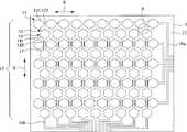
도면들 특히 도 1 및 2를 참조하면, 도 1은 본 발명의 제1 실시예에 따르는 정전용량식 터치 패널의 전도체 패턴 구조에 대한 설계도를 도시하고 도 2는 일반적으로 참조 부호 12로 지정되며, 기판(1)의 표면(11) 상에 형성되는 정전용량식 터치 패널의 전도체 패턴 구조의 일부분에 대한 투시도를 도시한다. 전도체 패턴 구조(12)는 "제1 축 전도체 어셈블리들"로 불려질, 제1 축을 따라 확장하는 복수의 전도체 어셈블리들(13), 및 "제2 축 전도체 어셈블리들"로 불려질, 제2 축을 따라 확장하는 복수의 전도체 어셈블리들(14)을 포함한다. 각각의 제1 축 전도체 어셈블리들(13)은 다른 제1 축 전도체 어셈블리들(13)에 평행하고, 각각의 제2 축 전도체 어셈블리들(14)은 다른 제2 축 어셈블리들(14)에 평행한다. 제1 축 전도체 어셈블리들(13)은 제2 축 전도체 어셈블리들(14)에 실질적으로 직각이다. 그러나, 제1 축 전도체 어셈블리들(13)과 제2 축 전도체 어셈블리들(14)은 직각(right angle) 이외인 그들 사이의 끼인각(included angle)으로 기판(1)의 표면(11) 상에 배열될 수 있음이 명백하다.
1 and 2, a schematic diagram of a conductive pattern structure of a capacitive touch panel according to a first embodiment of the present invention is shown. FIG. 2 is generally designated by
각각의 제1 축 전도체 어셈블리(13)는 실질적으로 동일하게 공간을 두는 방식으로 기판(1)의 표면(11) 상에, 도면에서 "X"로 표기되는, 제1 축을 따라 줄을 이루는 복수의 제1 축 전도체 셀들(131)로 구성되고, 배치 구역(15)은 인접한 제1 축 전도체 어셈블리들(13)과 인접한 제1 축 전도체 셀들(131) 사이로 범위가 정해진다. 제1 축(X)을 따라 제1 축 전도체 셀들(131)이 제1 축 전도체 어셈블리(13)를 형성하기 위해 함께 전기적으로 연결되도록 제1 축 전도 라인(132)은 제1 축(X)을 따라 위치되는 인접한 제1 축 전도체 셀들(131) 사이를 연결한다. 다시 말해서, 동일한 제1 축 어셈블리(13)의 제1 축 전도체 셀들(131)은 제1 축 전도 라인들(132)에 의해 직렬로 함께 연결된다. 각각의 제1 축 전도체 어셈블리(13)는 회로 기판 상에 배치되는 제어 회로(둘 다 도시되지 않음)로 신호를 전송하기 위한 신호 전송 라인(16a)에 더 연결된다.
Each of the first
각각의 전도 라인들(132)은 전기적 절연 특징을 포함하는 물질, 바람직하게는 이산화규소(silicon dioxide)와 같은 투명 절연 물질로 구성되는 절연 덮개층(17)에 의해 덮여지는 표면(133)을 갖는다. 각각의 제2 축 전도체 어셈블리(14)는, 기판(1)의 표면(11) 상에 실질적으로 동일하게 공간을 두는 방식으로, 도면들에서 "Y"로 표기되는, 제2 축을 따라 줄을 이루는 복수의 제2 축 전도체 셀들(141)로 구성된다. 각각의 제2 축 전도체 셀(141)은 각각의 제2 축 전도체 셀 배치 구역(15)에 설정된다.
Each of the
제2 축 전도 라인(142)은 동일한 제2 축 전도체 어셈블리(14)의 제2 축 전도체 셀들(141)이 서로 연결되도록 제2 축(Y)을 따라 위치되는 인접한 제2 축 전도체 셀들(141) 사이를 연결하고 각각의 절연층(17)의 표면에 위로 표면을 가로질러 확장한다. 다시 말해서, 동일한 제2 축 전도체 어셈블리(14)의 제2 축 전도체 셀들(141)은 제2 축 전도체 라인들(142)에 의해 직렬로 함께 연결된다. 각각의 제2 축 전도체 어셈블리(14)는 제어 회로로 신호를 전송하기 위한 신호 전송 라인(16b)에 더 연결된다.
The second
도 3을 참조하면, 이는 도 2의 3-3 선에 따르는 단면도를 도시하고 도 4는 도 2의 4-4 선에 따르는 단면도를 도시하며, 제1 축 전도체 셀들(131), 제1 축 전도 라인들(132), 제2 축 전도체 셀들(141), 및 제2 축 전도 라인들(142)는 투명 전도성 물질로 구성된다. 절연층(17)은 제2 축 전도체 어셈블리의 인접한 제2 축 전도체 셀들(141)을 연결하는 제2 축 전도 라인들(142)이 공통으로 절연되는 방식으로 각각 제1 축 전도 라인(132)을 가로질러 확장하도록 각각의 제1 축 전도 라인(132)과 제2 축 전도 라인(142) 사이에 배치된다.
3, which is a cross-sectional view taken along the line 3-3 in FIG. 2. FIG. 4 is a cross-sectional view taken along the line 4-4 in FIG. 2. The first
기판(1)은 유리 기판과 같은 강성 기판일 수 있고, 제1 축 전도체 어셈블리들(13)과 제2 축 전도체 어셈블리들(14), 및 제1 축과 제2 축 전도 라인들(132, 142)은 ITO 전도성 필름과 같은 투명 전도성 필름으로 구성된다. 도시된 실시예에서, 제1 축 전도체 셀들(131) 및 제2 축 전도체 셀들(141)은 실질적으로 6각형의 기하학적 윤곽의 형태이다. 전도체 셀들(131, 141)이 효과적인 전도체 표면의 최적 분포를 가져오기 위해 다른 기하학적 윤곽들의 형태들이 될 수 있음이 명백하다.
The
도 5는 본 발명에 따르는 정전용량식 터치 패널 상에서 사용자의 손가락이 물리적으로 접하는 지점을 보여주고, 도 6은 본 발명의 정전용량식 터치 패널 상에서 사용자의 손가락이 접하는 서로 다른 지점을 보여준다. 사용자가 본 발명의 정전용량식 터치 패널 상에서, "A"로 표기되는, 접촉 지역(지점)을 터치하기 위해 그의 또는 그녀의 손가락을 얹으면, 접촉 지역(A)에 의해 덮여지는, 제1 축 전도체 어셈블리(13)의 제1 축 전도체 셀(131) 및 제2 축 전도체 어셈블리(14)의 제2 축 전도체 셀(141)은 그들 사이의 커패시터 효과(capacitor effect)를 유도하고 그에 따라 야기되는 신호가 제어 회로에 신호 전송 라인들(16a, 16b)을 통해 전송된다. 제어 회로는 그리고 나서 기판(1)의 표면(11) 상의 어느 지점에 접촉 지역(A)이 설정되는지를 결정하기 위해 계산을 수행할 수 있다.
FIG. 5 shows a point where a user's finger is physically contacted on the capacitive touch panel according to the present invention, and FIG. 6 shows different points where a user's finger touches the capacitive touch panel of the present invention. When the user puts his or her finger on the capacitive touch panel of the present invention to touch the contact area (point), which is denoted by "A ", the first axis The first
사용자가 다른 접촉 지역(B)으로 그의 또는 그녀의 손가락을 움직일 때, 접촉 지역(B)에 의해 덮여지는, 제1 축 전도체 어셈블리(13)의 제1 축 전도체 셀(131) 및 제2 축 전도체 어셈블리(14)의 제2 축 전도체 셀(141)은 그들 사이의 커패시터 효과를 유도하고, 제어 회로로 신호 전송 라인들(16a, 16b)을 통해 전송되는 신호를 유도하는 변화가 발생한다. 제어 회로는 그리고 나서 기판(1)의 표면(11) 상의 어느 지점에 접촉 지역(B)이 설정되는지를 결정하기 위해 계산을 수행할 수 있다.
The first
도 7 및 8은 본 발명에 따르는 정전용량식 터치 패널의 전도체 패턴 제조 단계들을 보여주는 도식적인 설계도들로, 여기서 도 7은 복수의 제1 축 전도체 셀들(131), 제1 축 전도 라인들(132), 신호 전송 라인들(16a, 16b) 및 제2 축 전도체 셀들(141)이 방금 형성된 기판의 표면에 대한 도식도를 도시하고, 도 8은 도 7의 단계 이후에 각각의 제1 축 전도 라인(132)의 표면을 덮기 위해 절연 덮개층(17)이 형성되는 기판 표면에 대한 도식도를 도시한다. 또한, 도 9는, 본 발명에 따르는 터치 패널의 전도체 패턴 구조의 제조를 완료하도록, 도 8의 단계 이후에, 동일한 제2 축 전도체 어셈블리의 인접한 제2 축 전도체 셀들(141)의 각각의 쌍 사이를 연결하기 위해 제2 축 전도 라인(142)이 형성되는 기판 표면에 대한 도식도를 도시한다.
7 and 8 are schematic diagrams illustrating the steps of fabricating a conductive pattern of a capacitive touch panel in accordance with the present invention wherein FIG. 7 illustrates a plurality of first
전도체 패턴 구조(12)의 제조는 식각(etching), 스퍼터링(sputtering), 및 스크린 인쇄(screen printing)와 같은 임의의 알려진 기술들을 이용하여 수행될 수 있다. 다음과 같이 전도체 패턴 구조의 제조에 대한 예로써 식각이 수행된다. 우선, 일례로 ITO 투명 전도성 필름인 전도체 필름이 세정된 기판(1)의 표면(11) 상에 형성된다. 그 후에, 식각 마스크 인쇄 프로세스를 수행하기 위해 스크린 인쇄가 이용된다.
The fabrication of the
식각 마스크 인쇄 프로세스 이후에, 식각이 표면(11) 상에서 수행되며, 필름 스트리핑(stripping)이 뒤따른다. 따라서, 모두 투명하고 전기적을 전도성이 있는, 제1 축 전도체 어셈블리들(13)의 제1 축 전도체 셀들(131), 제1 전도 라인들(132), 및 제2 축 전도체 어셈블리들(14)의 제2 축 전도체 셀들(141)이, 도 7에 도시된 바와 같이, 기판 표면(11) 상에 형성된다. 이 시점에서, 동일한 제1 축 전도체 어셈블리들(13)의 모든 제1 축 전도체 셀들(131)은 함께 전기적으로 연결되고 제1 축 전도체 어셈블리들(13)은 복수의 신호 전송 라인들(16a)에 더 연결된다.
After the etching mask printing process, etching is performed on the
그 후에, 도 8에 도시된 바와 같이, 각각의 제1 축 전도 라인(132)의 표면(133)을 덮기 위해 절연 덮개층(17)이 적용된다. 그리고 나서, 제2 축 전도 라인들(142)의 위치들을 정하기 위해 인쇄 기술을 이용하여 마스크가 형성되며, 도 9에 도시된 바와 같이, 제2 축(Y)을 따라 인접한 제2 축 전도체 셀들(141)이 각각의 절연층(17)의 표면에 위로 가로질러 확장하는 각각의 제2 축 전도 라인(142)을 이용하여 제2 축 전도 라인들(142)에 의해 각각 연결되는 제2 축 전도 라인들(142)을 형성하기 위해 투명 전도층의 적용이 뒤따른다. 일단 상기 단계가 완료되면, 동일한 제2 축 전도체 어셈블리들(14)의 모든 제2 축 전도체 셀들(141)은 함께 전기적으로 연결되고 제2 축 전도체 어셈블리들(14)은 신호 전송 라인들(16b)에 연결된다.
Thereafter, as shown in FIG. 8, an insulating
상기에서 설명된 식각 기술이 기판 표면 상에 전도체 셀들 및 전도 라인들을 형성하기 위해 쓰일 때, 전도체 패턴 구조를 유사하게 형성하기 위해 서로 다른 식각 마스크들에 의해 정해지는 식각 지역들에 서로 다른 패턴이 형성될 수 있다. 예를 들어, 제1 식각 단계에서, 오직 제1 축 전도체 어셈블리들(13)의 제1 축 전도체 셀들(131) 및 제1 축 전도 라인들(132)만이 기판 표면(11) 상에 형성되고, 제2 축 전도체 어셈블리들(14)의 제2 축 전도체 셀들(141)은 형성되지 않는다. 그 후에, 관련된 절연층들(17)의 표면들에 위로 가로질러 확장하는 제2 층 전도 라인들(142)을 갖는, 기판 표면(11) 상에 제2 축 전도체 셀들(141) 및 제2 축 전도 라인들(142)을 형성하기 위해 동일한 식각 기술이 다시 쓰인다.
When the etch techniques described above are used to form conductive cells and conductive lines on a substrate surface, different patterns are formed in etched areas defined by different etch masks to similarly form a conductor pattern structure . For example, in the first etching step, only the first
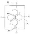
이전에 논의된 실시예에서, 제1 축 전도체 셀들 및 제2 축 전도체 셀들은 정전용량식 터치 패널의 전도체 패턴 구조를 구성하기 위해 어레이 형태로 기판 상에 각각 형성된다. 동일한 원리에 기초하여, 소수의 전도체 셀들이 또한 정전용량식 터치 패널의 전도체 패턴 구조를 구성하기 위해 사용될 수 있다. 이는 개시된 본 발명의 제2 실시예로써 도 10에 도시되어 있는데, 여기서 2개의 인접한 제1 축 전도체 셀들(31, 32)이 기판(2)의 표면(21) 상에 형성되고 신호 전송 라인(34)은 전도체 셀(32)에 연결된다. 제1 축 전도 라인(33)은 인접한 제1 축 전도체 셀들(31, 32) 사이를 연결한다. 절연층(4)은 제1 축 전도 라인(33)의 표면 상에 형성된다.
In the previously discussed embodiment, the first axis conductor cells and the second axis conductor cells are each formed on the substrate in the form of an array to form a conductor pattern structure of the capacitive touch panel. Based on the same principle, a small number of conductor cells can also be used to construct the conductor pattern structure of the capacitive touch panel. This is shown in FIG. 10 as a second embodiment of the disclosed invention wherein two adjacent first
축을 따라, 제1 축 전도체 셀들(31, 32)과는 다른 2개의 인접한 제2 축 전도체 셀들(51, 52)이 배열되고 제2 축 전도 라인들(53)은 절연층(4)의 표면 위로 가로질러 확장하여 인접한 제2 축 전도체 셀들(51, 52)를 연결한다. 전도체 셀(52)은 또한 신호 전송 라인(54)에 연결된다.
Two adjacent second
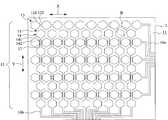
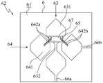
도 11을 참조하면, 본 발명의 제3 실시예에 따르는 정전용량식 터치 패널의 전도체 패턴 구조에 대한 설계도가 도시된다. 일반적으로 참조 번호 62로 표기되는 전도체 패턴 구조가 유리 기판과 같은 강성 기판(6)의 표면(61) 상에 형성된다. 전도체 패턴 구조(62)는, 매트릭스 구조를 형성하는, 복수의 제1 축 전도체 어셈블리들(63) 및 복수의 제2 축 전도체 어셈블리들(64)을 더 포함한다. 각각의 제1 축 전도체 어셈블리들(63)은 다른 제1 축 전도체 어셈블리들(63)에 평행하고, 각각의 제2 축 전도체 어셈블리들(64)은 다른 제2 축 전도체 어셈블리들(64)에 평행한다. 제1 축 전도체 어셈블리들(63)은 제2 축 전도체 어셈블리들(64)에 실질적으로 직각이다. 그러나, 제1 축 전도체 어셈블리들(63) 및 제2 축 전도체 어셈블리들(64)은 직각 이외인 그들 사이의 끼인각으로 기판(6)의 표면(61) 상에 배열될 수 있음이 명백하다.
Referring to FIG. 11, a schematic diagram of a conductive pattern structure of a capacitive touch panel according to a third embodiment of the present invention is shown. A conductor pattern structure, generally designated by
각각의 제1 축 전도체 어셈블리(63)는, 실질적으로 동일하게 공간을 두는 방식으로 강성 기판(6)의 표면(61) 상에, 수직 방향과 같은, 제1 축 방향을 따라 줄을 이루는 복수의 제1 축 전도체 셀들(631)을 포함한다. 각각의 제2 축 전도체 어셈블리(64)는, 실질적으로 동일하게 공간을 두는 방식으로 제2 축을 따라 강성 기판(6)의 표면(61) 상에 배열되는, 수평 방향과 같은, 제2 축을 따라 줄을 이루는 복수의 제2 축 전도체 셀들(641)을 포함한다.
Each of the first
각각 각각의 제1 축 전도체 어셈블리(63)의 제1 축 전도체 셀들(631)이 서로 전기적으로 연결되도록 복수의 제1 축 전도 라인들(632)은 각각의 제1 축 전도체 어셈블리들(63)의 인접한 제1 축 전도체 셀들(631)을 각각 연결한다. 제1 축 전도체 어셈블리들(63)을 형성하기 위해 제1 축을 따라 제1 축 전도체 셀들(631)이 전기적으로 연결되도록 제1 축 전도 라인(632)은 제1 축을 따라 위치되는 인접한 제1 축 전도체 셀들(631)을 연결한다. 다시 말해서, 동일한 제1 축 전도체 어셈블리(63)의 제1 축 전도체 셀들(631)은 제1 축 전도 라인들(632)에 의해 직렬로 함께 연결된다. 각각의 제1 축 전도체 어셈블리(63)는 회로 기판 상에 배치되는 제어 회로(둘 다 도시되지 않음)에 제1 축 신호를 전송하기 위한 제1 축 신호 전송 라인(66a)에 더 연결된다.
A plurality of first axis
각각 각각의 제2 축 전도체 어셈블리(64)의 제2 축 전도체 셀들(641)이 서로 전기적으로 연결되도록 복수의 제2 축 전도 라인들(642)은 각각의 제2 축 전도체 어셈블리(64)의 인접한 제2 축 전도체 셀들(641)을 각각 연결한다. 다시 말해서, 동일한 제2 축 전도체 어셈블리(64)의 제2 축 전도체 셀들(641)은 제2 축 전도 라인들(642)에 의해 직렬로 연결된다. 각각의 제2 축 전도체 어셈블리(64)는 제어 회로에 제2 축 신호를 전송하기 위한 제2 축 신호 전송 라인(66b)에 더 연결된다. 또한, 각각의 제2 축 전도 라인들(642)은 각각 인접한 제1 축 전도체 셀(631)의 적어도 일부분 위에 위치하고 제2 축 전도 라인(642)은 인접한 제1 축 전도 라인(632)과 교차하지 않는다.
A plurality of second axial
또한, 제1 축 전도성 어셈블리들(63)을 제2 축 전도성 어셈블리들(64)로부터 절연시키기 위해, 복수의 절연체들(65)이 제2 축 전도 라인(642)와 인접한 제1 축 전도체 셀(631) 사이에 배치되며, 제2 축 전도 라인(642)은 제2 축 전도 라인(642)과 인접한 제1 축 전도체 셀(631) 사이의 전자적 연결을 방지하기 위한 복수의 절연체들(65) 위에 위치한다. 제2 축 전도 라인(642)은 각각 인접한 절연체(65)를 가로질러 확장한다.
A plurality of
도 12는 본 발명의 제4 실시예에 따르는 정전용량식 터치 패널의 전도체 패턴 구조에 대한 설계도를 도시한다. 제4 실시예의 전도체 패턴 구조는 제3 실시예의 전도체 패턴 구조와 원칙적으로 매우 유사하다. 제3 실시예에서는, 인접한 제2 축 전도체 셀들(641) 사이에 배치되는 오직 하나의 제2 축 전도 라인(642)이 있다. 다시 말해서, 제2 축 전도성 어셈블리들(64)의 인접한 제2 축 전도체 셀들(641)은 제2 축 전도 라인(642)에 의해 서로 연결된다. 제3 실시예와 비교하여, 제4 실시예는 제2 축 전도체 셀들(641)의 인접한 것들을 서로 연결하기 위해 2개의 제2 축 전도 라인들(642)을 사용한다. 이러한 경우에, 제2 축 저도 라인들(642) 중의 하나가 고장나거나 효율적으로 작동하지 않을 경우, 다른 제2 축 전도 라인(642)이 여전히 작동할 수 있고, 따라서 전도체 패턴 구조의 안정성이 개선된다. 그러므로, 정전용량식 터치 패널의 성능이 향상된다.
12 shows a schematic diagram of a conductive pattern structure of a capacitive touch panel according to a fourth embodiment of the present invention. The conductor pattern structure of the fourth embodiment is in principle very similar to the conductor pattern structure of the third embodiment in principle. In the third embodiment, there is only one second
도 13을 참조하면, 본 발명의 제5 실시예에 따르는 정전용량식 터치 패널의 전도체 패턴 구조에 대한 설계도가 도시된다. 제5 실시예의 전도체 패턴 구조는 제4 실시예의 전도체 패턴 구조와 원칙적으로 매우 유사하다. 제4 실시예에서, 2개의 제2 축 전도 라인들(642)은 둘 다 동일한 인접한 제1 축 전도체 셀(631) 위에 위치한다. 다시 말해서, 2개의 제2 축 전도 라인들(642)은 둘 다 인접한 제1 축 전도 라인(632)의 동일한 측(side) 상에 배치된다. 제4 실시예와 비교하여, 제5 실시예의 2개의 제2 축 전도 라인들(642)은 서로 다른 인접한 제1 축 전도체 셀들(631) 위에 위치하고, 인접한 제1 축 전도 라인(632)은 2개의 제2 축 전도 라인들(642) 사이에 있다. 이러한 경우에, 2개의 제2 축 전도 라인들(642)이 서로 다른 인접한 제1 축 전도체 셀들(631)을 덮기 때문에, 제1 전도체 셀들(631) 중의 하나에서 외력(external force)으로 인해 제2 전도 라인들(642) 중의 하나가 고장날 경우에, 다른 제2 전도 라인들(642)이 여전히 작동할 수 있고, 따라서, 전도체 패턴 구조의 압력에 대한 저항이 그에 따라 개선된다. 그러므로, 정전용량식 터치 패널의 성능이 크게 향상된다.
Referring to FIG. 13, a schematic diagram of a conductive pattern structure of a capacitive touch panel according to a fifth embodiment of the present invention is shown. The conductor pattern structure of the fifth embodiment is in principle very similar to the conductor pattern structure of the fourth embodiment in principle. In the fourth embodiment, the two second
상기 언급된 제3, 제4 및 제5 실시예에서, 제2 축 전도 라인(642)은 직선이거나 곡선과 같은 비 직선(non-straight line) 또는 굽은 선(meander-line)일 수 있다. 도 14는 제2 축 전도 라인(642)이 굽은 선인 전도체 패턴 구조의 제6 실시예를 도시한다. 제6 실시예의 전도체 패턴 구조는 제5 실시예의 전도체 패턴 구조와 원칙적으로 매우 유사하다. 제5 실시예에서, 2개의 제2 축 전도 라인들(642)는 모두 직선들인데 반해; 제6 실시예에서, 2개의 제2 축 전도 라인들(642)은 비 직선들이다. 상기에서 언급한 제4 및 제5 실시예들에서, 2개의 제2 축 전도 라인(642)은 실질적으로 서로 직각이거나 각을 이룰 수 있다. 또한, 제4, 제5 및 제6 실시예들에서, 또 다른 상황은 제2 축 전도 라인(642) 중의 오직 하나만이 직선이고 다른 제2 축 전도 라인(642)은 비 직선이라는 것이다. 더불어, 제4, 제5 및 제6 실시예들에서, 전도체 패턴 구조는 인접한 제2 축 전도체 셀들(641)을 전자적으로 서로 연결하는 3개 또는 그 이상의 제2 축 전도 라인들(642)을 사용할 수 있다.
In the above-described third, fourth and fifth embodiments, the second axial
제2 축 전도 라인(642)이 더 길어질수록 제조 및 사용 과정에서 더 쉽게 고장하는 것으로 잘 알려져 있다. 그러므로, 도 15는 제2 축 전도 라인(642)이 길어지는 문제를 해결하기 위한 전도체 패턴 구조에 대한 제7 실시예를 도시한다. 제7 실시예의 전도체 패턴 구조는 제3 실시예의 전도체 패턴 구조와 원칙적으로 매우 유사하다. 제3 실시예에는, 오직 인접한 제2 축 전도체 셀들(641) 사이에 배치되는 긴 제2 축 전도 라인(642)만이 있다. 제7 실시예의 각각의 제2 전도 라인들(642)은 제1 브랜치(branch, 642a) 및 제2 브랜치(642b)를 가지며, 제1 브랜치(642a)는 여기서 제2 브랜치(642b)와 분리되어 있는 것임이 도 15에서 명확히 보일 수 있다. 도 15에서 도시되는 전도체 패턴 구조는 각각 복수의 절연체들(65) 상에 또한 배치되는 복수의 전기적 연결 소자들(67)을 더 포함한다. 제1 브랜치(642a)는 인접한 절연체(65) 상에 배치되는 전기적 연결 소자(67)에 전자적으로 연결되고, 제2 브랜치(642b)는 또한 인접한 절연체(65) 상에 배치되는 전기적 연결 소자(66)에 전자적으로 연결된다. 따라서, 인접한 제2 축 전도체 셀들(641)은 제1 브랜치(642a), 전기적 연결 소자(67) 및 제2 브랜치(642b)의 조합에 의해 전자적으로 연결된다.
It is well known that the longer the second
상기에서 언급한 제7 실시예에서, 긴 제2 축 전도 라인(642)은 2개의 짧은 분리된 브랜치들(642a 및 642b)로 나누어진다. 이러한 경우에, 더 긴 제2 축 전도 라인(642)과 비교하여, 2개의 분리된 브랜치들(642a 및 642b)가 고장나는 것이 쉽지 않고, 전도체 패턴 구조의 수율(yield)이 증가된다. 그러므로, 터치 패널의 성능이 그에 따라 향상된다.
In the above-mentioned seventh embodiment, the long second axis
도 16을 참조하면, 본 발명의 제8 실시예에 따라는 정전용량식 터치 패널의 전도체 패턴 구조에 대한 설계도가 도시된다. 제8 실시예의 전도체 패턴 구조(62)는 제7 실시예의 전도체 패턴 구조(62)와 원칙적으로 매우 유사하다. 제7 실시예에서는, 인접한 제2 축 전도체 셀들(641) 사이에 배치되는 오직 하나의 제2 축 전도 라인(642)만이 있다. 다시 말해서, 제2 축 전도성 어셈블리(64)의 인접한 제2 축 전도체 셀들(641)은 제2 축 전도 라인(642)에 의해 서로 연결된다. 제7 실시예와 비교하여, 제8 실시예는 인접한 제2 축 전도체 셀들(641)을 서로 연결하기 위해 2개의 제2 축 전도 라인들(642)을 사용한다. 각각의 제2 축 전도 라인들(642)은 제1 브랜치(642a) 및 제2 브랜치(642b)를 포함한다. 각각의 제2 전도 라인(642)의 제1 브랜치(642a) 및 제2 브랜치(642b)는 서로에게서 분리되고, 2개의 제2 축 전도 라인들(642)의 제1 브랜치(642a) 및 제2 브랜치(642b)는 인접한 절연체(65) 상에 배치되는 전기적 연결 소자(67)와 전자적으로 연결된다. 2개의 제2 축 전도 라인들은 동일한 인접한 제1 축 전도체 셀(631) 상에 위치한다. 이러한 경우에, 제2 축 전도 라인들(642) 중의 하나가 고장나거나 효과적으로 작동하지 않을 시에, 다른 제2 축 전도 라인(642)이 여전히 작동할 수 있고, 따라서 전도체 패턴 구조의 안정성이 개선된다. 그러므로, 정전용량식 터치 패널의 성능이 향상된다.
Referring to FIG. 16, a schematic diagram of a conductive pattern structure of a capacitive touch panel according to an eighth embodiment of the present invention is shown. The
도 17은 본 발명의 제9 실시예에 따르는 정전용량식 터치 패널의 전도체 패턴 구조에 대한 설계도를 도시한다. 제9 실시예의 전도체 패턴 구조는 제8 실시예의 전도체 패턴 구조와 원칙적으로 매우 유사하다. 제8 실시예에서는, 2개의 제2 축 전도 라인들(642)이 모두 동일한 인접한 제1 축 전도체 셀들((631) 위에 위치한다. 다시 말해서, 2개의 제2 축 전도 라인들(642)은 모두 인접한 제1 축 전도 라인(632)의 동일한 측에 배치된다. 제8 실시예와 비교하여, 제9 실시예의 2개의 제2 축 전도 라인들(642)은 서로 다른 인접한 제1 축 전도체 셀들(631) 위에 위치하고, 인접한 제1 축 전도 라인(632)은 2개의 제2 축 전도 라인들(642) 사이에 있다. 각각의 제2 축 전도 라인들(642)은 제1 브랜치(642a) 및 제2 브랜치(642b)를 포함한다. 각각의 제2 전도 라인(642)의 제1 브랜치(642a) 및 제2 브랜치(642b)는 서로에게서 분리되고, 2개의 제2 축 전도 라인들(642)의 제1 브랜치(642a) 및 제2 브랜치(642b)는 서로 다른 인접한 절연체들(65) 상에 베치되는 서로 다른 전기적 연결 소자들(67)에 전자적으로 연결된다. 이러한 경우에, 2개의 제2 축 전도 라인들(642)이 서로 다른 인접한 제1 축 전도체 셀들(631)을 덮기 때문에, 제2 전도 라인들(642) 중의 하나가 제1 전도체 셀들(631) 중의 하나에서의 외력으로 인해 고장날 시에, 다른 제2 전도 라인들(642)이 여전히 작동할 수 있고, 따라서, 전도체 패턴 구조의 압력에 대한 저항이 그에 따라 개선된다. 그러므로, 정전용량식 터치 패널의 성능이 크게 향상된다.
17 shows a design diagram of a conductive pattern structure of a capacitive touch panel according to a ninth embodiment of the present invention. The conductor pattern structure of the ninth embodiment is very similar in principle to the conductor pattern structure of the eighth embodiment. In the eighth embodiment, the two second axial
상기에서 언급한 제7, 제8 및 제9 실시예들에서, 제2 축 전도 라인(642)은 직선 또는 곡선과 같은 비 직선 또는 굽은 선일 수 있다. 비 직선은 도 14에 도시된 실시예와 같을 수 있다. 또한, 제8 및 제9 실시예에서, 제2 축 전도 라인(642) 중 오직 하나만이 직선이고 다른 제2 축 전도 라인(642)은 비 직선인 또 다른 경우가 있다. 더불어, 제8 및 제9 실시예들에서, 전도체 패턴 구조는 인접한 제2 축 전도체 셀들(641)을 전자적으로 서로 연결하는 3개 또는 그 이상의 제2 축 전도 라인들(642)을 사용할 수 있다.
In the above-mentioned seventh, eighth and ninth embodiments, the second axial
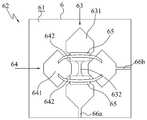
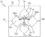
이 부분에서는, 2개의 분리된 브랜치들을 갖는 제2 축 전도 라인들을 이용하는 다른 실시예들이 묘사될 것이다. 도 18을 참조하면, 본 발명의 제10 실시예에 따르는 정전용량식 터치 패널의 전도체 패턴 구조에 대한 설계도가 도시된다. 일반적으로 참조 부호 72로 표시되는 전도체 패턴 구조는 유리 기판과 같은 기판(7)의 표면(71) 상에 형성된다. 전도체 패턴 구조(72)는, 매트릭스 구조를 형성하는, 복수의 제1 축 전도체 어셈블리들(73) 및 복수의 제2 축 전도체 어셈블리들(74)을 더 포함한다. 각각의 제1 축 전도체 어셈블리들(73)은 다른 제1 축 전도체 어셈블리들(73)에 평행하고, 각각의 제2 축 전도체 어셈블리들(74)은 다른 제2 축 전도체 어셈블리들(74)에 평행한다. 제1 축 전도체 어셈블리들(73)은 제2 축 전도체 어셈블리들(74)에 실질적으로 직각이다. 그러나, 제1 축 전도체 어셈블리들(73)과 제2 축 전도체 어셈블리들(74)이 직각 이외에 그들 사이의 끼인각으로 기판(7)의 표면(71) 상에 배열될 수 있음이 명백하다.
In this section, other embodiments utilizing second shaft conduction lines having two separate branches will be described. Referring to Fig. 18, a schematic diagram of a conductor pattern structure of a capacitive touch panel according to a tenth embodiment of the present invention is shown. The conductor pattern structure, generally designated 72, is formed on the
각각의 제1 축 전도체 어셈블리(73)는, 실질적으로 동일하게 공간을 두는 방식으로 기판(7)의 표면(71) 상에, 수직 방향과 같은, 제1 축을 따라 줄을 이루는 복수의 제1 축 전도체 셀들(731)을 포함한다. 각각의 제2 축 전도체 어셈블리(74)는, 실질적으로 동일하게 공간을 두는 방식으로 제2 축을 따라 기판(7)의 표면(71) 상에 배열되는, 수평 방향과 같은, 제2 축을 따라 줄을 이루는 복수의 제2 축 전도체 셀들(741)을 포함한다.
Each of the first
각각 각각의 제1 축 전도체 어셈블리(73)의 제1 축 전도체 셀들(731)이 서로 전기적으로 연결되도록 복수의 제1 축 전도 라인들(732)은 각각의 제1 축 전도체 어셈블리들(73)의 인접한 제1 축 전도체 셀들(731)을 각각 연결한다. 제1 축 전도체 어셈블리(73)를 형성하기 위해 제1 축을 따라 제1 축 전도체 셀들(731)이 전기적으로 연결되도록 제1 축 전도 라인(732)은 제1 축을 따라 위치되는 인접한 제1 축 전도체 셀들(731)을 연결한다. 다시 말해서, 동일한 제1 축 전도체 어셈블리(73)의 제1 축 전도체 셀들(731)은 제1 축 전도 라인들(732)에 의해 직렬로 함께 연결된다. 각각의 제1 축 전도체 어셈블리(73)는 회로 기판 상에 배치되는 제어 회로(둘 다 도시되지 않음)에 제1 축 신호를 전송하기 위한 제1 축 신호 전송 라인(76a)에 더 연결된다.
The plurality of first
복수의 전기적 연결 소자들(77)은 각각 복수의 제1 축 전도체 셀(731) 옆에 배치되고, 각각의 전기적 연결 소자들(77)은 인접한 제1 축 전도체 셀(731)로부터 절연된다. 전기적 연결 소자(77)는 인접한 제1 축 전도체 셀(731)의 일부분처럼 보인다.
A plurality of electrical connecting
각각 각각의 제2 축 전도체 어셈블리(74)의 제2 축 전도체 셀들(741)이 서로 전기적으로 연결되도록 복수의 제2 축 전도 라인들(742)은 각각의 제2 축 전도체 어셈블리(74)의 인접한 제2 축 전도체 셀들(741)을 각각 연결한다. 제10 실시예의 각각의 제2 전도 라인들(742)은 제1 브랜치(742a) 및 제2 브랜치(742b)를 가지고, 여기서 제1 브랜치(742a)와 제2 브랜치(742b)는 분리된 것들임이 도 18에서 명확히 보일 수 있다. 제2 축 전도 라인(742)의 제1 브랜치(742a) 및 제2 브랜치(742b)는 인접한 전기적 연결 소자(77)에 전자적으로 연결되고 바람직하게는 인접한 제1 축 전도 라인(732)과 겹치지 않는다. 따라서, 인접한 제2 축 전도체 셀들(741)은 제2 축 전도 라인(742)의 제1 브랜치(742a), 제2 브랜치(742b) 및 전기적 연결 소자(77)의 조합에 의해 전자적으로 연결된다.
A plurality of second axial conductive lines 742 are disposed adjacent to each of the second
다시 말해서, 동일한 제2 축 전도체 어셈블리(74)의 제2 축 전도체 셀들(741)은 제2 축 전도 라인들(742)에 의해 직렬로 연결된다. 각각의 제2 축 전도체 어셈블리(74)는 제어 회로로 제2 축 신호를 전송하기 위한 제2 축 신호 전송 라인(76b)에 더 연결된다. 또한, 각각의 제2 축 전도 라인들(742)은 각각 인접한 제1 축 전도 라인(732)의 적어도 일부분 위에 위치한다.
In other words, the second
또한, 제1 축 전도성 어셈블리들(73)을 제2 축 전도성 어셈블리들(74)로부터 절연시키기 위해, 복수의 절연체들(75)이 제1 축 전도 라인들(732)과 전기적 연결 소자(77) 사이에 배치되며, 복수의 절연체들(75)은, 제1 축 전도 라인들(732)과 전기적 연결 소자(77) 사이의 전자적 연결을 방지하고, 또한 제1 축 전도 라인(732)과 제2 축 전도 라인(742) 사이의 전자적 연결을 방지하기 위해, 각각 전기적 연결 소자(77) 위에 위치한다. 제2 축 전도 라인(742)은 각각 인접한 절연체(75)를 가로질러 확장한다.
A plurality of
도 19는 본 발명의 제11 실시예에 따르는 정전용량식 터치 패널의 전도체 패턴 구조에 대한 설계도를 도시한다. 제11 실시예의 전도체 패턴 구조(72)는 제10 실시예의 전도체 패턴 구조(72)와 원칙적으로 매우 유사하다. 제10 실시예에서는, 인접한 제2 축 전도체 셀들(741) 사이에 배치되는 오직 하나의 제2 축 전도 라인(742)이 있다. 다시 말해서, 제2 축 전도성 어셈블리들(74)의 인접한 제2 축 전도체 셀들(741)은 제2 축 전도 라인(742)에 의해 서로 연결된다. 제10 실시예와 비교하여, 제11 실시예는 제2 축 전도체 셀들(741)의 인접한 제2 축 전도체 셀들(741) 서로 연결하기 위해 2개의 제2 축 전도 라인들(742)을 사용한다. 각각의 제2 축 전도 라인들(742)은 제1 브랜치(742a) 및 제2 브랜치(742b)를 포함한다. 각각의 제2 전도 라인(742)의 제1 브랜치(742a) 및 제2 브랜치(742b)는 서로에게서 분리되고, 2개의 제2 축 전도 라인들(742)의 제1 브랜치(742a) 및 제2 브랜치(742b)는 각각 인접한 제1 축 전도체 셀들(731) 옆에 배치되는 동일한 전기적 연결 소자(77)와 전자적으로 연결된다. 2개의 제2 축 전도 라인들(742)은 동일한 인접한 전기적 연결 소자(77) 위에 위치한다. 이러한 경우에, 제2 축 저도 라인들(742) 중의 하나가 고장나거나 효율적으로 작동하지 않을 시에, 다른 제2 축 전도 라인(742)이 여전히 작동할 수 있고, 따라서 전도체 패턴 구조의 안정성이 개선된다. 그러므로, 정전용량식 터치 패널의 성능이 향상된다.
19 shows a schematic diagram of a conductor pattern structure of a capacitive touch panel according to an eleventh embodiment of the present invention. The
도 20을 참조하면, 본 발명의 제12 실시예에 따르는 정전용량식 터치 패널의 전도체 패턴 구조에 대한 설계도가 도시된다. 제12 실시예의 전도체 패턴 구조는 제11 실시예의 전도체 패턴 구조와 원칙적으로 매우 유사하다. 제11 실시예에서, 2개의 제2 축 전도 라인들(742)은 둘 다 동일한 인접한 전기적 연결 소자(77) 위에 위치한다. 다시 말해서, 2개의 제2 축 전도 라인들(742)은 둘 다 인접한 제1 축 전도 라인(732)의 동일한 측 상에 배치된다. 제11 실시예와 비교하여, 제12 실시예의 2개의 제2 축 전도 라인들(742)은 서로 다른 인접한 전기적 연결 소자들(77) 위에 위치하고, 인접한 제1 축 전도 라인(732)은 2개의 제2 축 전도 라인들(742) 사이에 있다. 각각의 제2 축 전도 라인들(742)은 제1 브랜치(742a) 및 제2 브랜치(742b)를 포함한다. 각각의 제2 전도 라인(742)의 제1 브랜치(742a) 및 제2 브랜치(742b)는 서로에게서 분리되고, 2개의 제2 축 전도 라인들(742)의 제1 브랜치(742a) 및 제2 브랜치(742b)는 서로 다른 인접한 전기적 연결 소자들(77)에 전자적으로 연결된다. 이러한 경우에, 2개의 제2 축 전도 라인들(742)이 서로 다른 인접한 전기적 연결 소자들(77)을 덮기 때문에, 제1 전도체 셀들(731) 중의 하나에서 외력으로 인해 제2 전도 라인들(742) 중의 하나가 고장날 경우에, 다른 제2 전도 라인들(742)이 여전히 작동할 수 있고, 따라서, 전도체 패턴 구조의 압력에 대한 저항이 그에 따라 개선된다. 그러므로, 정전용량식 터치 패널의 성능이 크게 향상된다.
Referring to FIG. 20, a schematic diagram of a conductive pattern structure of a capacitive touch panel according to a twelfth embodiment of the present invention is shown. The conductor pattern structure of the twelfth embodiment is in principle very similar to the conductor pattern structure of the eleventh embodiment. In the eleventh embodiment, the two second shaft conduction lines 742 are both located on the same adjacent electrical connecting
상기에서 언급된 제10, 제11 및 제12 실시예에서, 기판(7)은 유리 기판과 같은 강성 기판, 또는 플라스틱 기판과 같은 연성 기판(flexible substrate) 또는 다른 투명 절연 기판들일 수 있다. 제2 축 전도 라인(742)은 직선이거나 곡선과 같은 비 직선 또는 굽은 선일 수 있다. 비 직선은 도 14에 도시된 실시예와 같을 수 있다. 또한, 제11 및 제12 실시예에서, 제2 축 전도 라인(742) 중 오직 하나만이 직선이고 다른 제2 축 전도 라인(742)은 비 직선인 또 다른 경우가 있다. 더불어, 제11 및 제12 실시예들에서, 전도체 패턴 구조(72)는 인접한 제2 축 전도체 셀들(741)을 전자적으로 서로 연결하는 3개 또는 그 이상의 전도 라인들(742)을 사용할 수 있다.
In the above-mentioned tenth, eleventh and twelfth embodiments, the
도 21을 참조하면, 본 발명의 제13 실시예에 따르는 정전용량식 터치 패널의 전도체 패턴 구조에 대한 설계도가 도시된다. 일반적으로 참조 부호 82로 표시되는 전도체 패턴 구조는 유리 기판과 같은 기판(8)의 표면(81) 상에 형성된다. 전도체 패턴 구조(82)는, 매트릭스 구조를 형성하는, 복수의 제1 축 전도체 어셈블리들(83) 및 복수의 제2 축 전도체 어셈블리들(74)을 더 포함한다. 각각의 제1 축 전도체 어셈블리들(83)은 다른 제1 축 전도체 어셈블리들(83)에 평행하고, 각각의 제2 축 전도체 어셈블리들(84)은 다른 제2 축 전도체 어셈블리들(84)에 평행한다. 제1 축 전도체 어셈블리들(83)은 제2 축 전도체 어셈블리들(84)에 실질적으로 직각이다. 그러나, 제1 축 전도체 어셈블리들(83)과 제2 축 전도체 어셈블리들(84)은 직각 이외에 그들 사이의 끼인각으로 기판(8)의 표면(81) 상에 배열될 수 있음이 명백하다.
Referring to FIG. 21, a schematic diagram of a conductive pattern structure of a capacitive touch panel according to a thirteenth embodiment of the present invention is shown. A conductor pattern structure, generally designated by the
각각의 제1 축 전도체 어셈블리(83)는, 실질적으로 동일하게 공간을 두는 방식으로 기판(8)의 표면(81) 상에 배열되는, 수직 방향과 같은, 제1 축을 따라 줄을 이루는 복수의 제1 축 전도체 셀들(831)을 포함한다. 각각의 제2 축 전도체 어셈블리(84)는, 실질적으로 동일하게 공간을 두는 방식으로 제2 축을 따라 기판(8)의 표면(81) 상에 배열되는, 수평 방향과 같은, 제2 축을 따라 줄을 이루는 복수의 제2 축 전도체 셀들(841)을 포함한다.
Each of the first
각각의 제1 축 전도체 셀들(831)은 윈도우(window, 831a)를 가지고, 복수의 전기적 연결 소자들(87)은 각각 윈도우들 안에 배치된다. 제1 축 전도체 셀(831)과 전기적 연결 소자(87) 사이에 갭(831b)이 있어서 그들은 전자적으로 연결되지 않는다.
Each first
각각 각각의 제1 축 전도체 어셈블리(83)의 제1 축 전도체 셀들(831)이 서로 전기적으로 연결되도록 복수의 제1 축 전도 라인들(832)은 각각의 제1 축 전도체 어셈블리들(83)의 인접한 제1 축 전도체 셀들(831)을 각각 연결한다. 제1 축 전도체 어셈블리들(83)이 형성하기 위해 제1 축을 따라 제1 축 전도체 셀들(831)이 전기적으로 연결되도록 제1 축 전도 라인(832)은 제1 축을 따라 위치되는 인접한 제1 축 전도체 셀들(831)을 연결한다. 다시 말해서, 동일한 제1 축 전도체 어셈블리(83)의 제1 축 전도체 셀들(831)은 제1 축 전도 라인들(832)에 의해 직렬로 함께 연결된다. 각각의 제1 축 전도체 어셈블리(83)는 회로 기판 상에 배치되는 제어 회로(둘 다 도시되지 않음)에 제1 축 신호를 전송하기 위한 제1 축 신호 전송 라인(86a)에 더 연결된다.
A plurality of first axis
각각 각각의 제2 축 전도체 어셈블리(84)의 제2 축 전도체 셀들(841)이 서로 전기적으로 연결되도록 복수의 제2 축 전도 라인들(842)은 각각의 제2 축 전도체 어셈블리(84)의 인접한 제2 축 전도체 셀들(841)을 각각 연결한다. 제13 실시예의 각각의 제2 전도 라인들(842)은 제1 브랜치(842a) 및 제2 브랜치(842b)를 가지고, 여기서 제1 브랜치(842a) 및 제2 브랜치(842b)는 분리된 것들임이 도 21에서 명확히 보일 수 있다. 각각의 제2 축 전도 라인(842)의 제1 브랜치(842a) 및 제2 브랜치(842b)는 각각 전기적 연결 소자(87)에 전자적으로 연결된다. 따라서, 인접한 제2 축 전도체 셀들(841)은 제2 축 전도 라인(842)의 제1 브랜치(842a), 제2 브랜치(842b) 및 인접한 제1 축 전도체 셀(831)의 윈도우(831a) 내에 배치되는 전기적 연결 소자(87)의 조합에 의해 전자적으로 연결된다.
A plurality of second axial conduction lines 842 are disposed adjacent to each other of the second
다시 말해서, 동일한 제2 축 전도체 어셈블리(84)의 제2 축 전도체 셀들(841)은 제2 축 전도 라인들(842)에 의해 직렬로 연결된다. 각각의 제2 축 전도체 어셈블리(84) 제어 회로로 제2 축 신호를 전송하기 위한 제2 축 신호 전송 라인(86b)에 더 연결된다. 또한, 각각의 제2 축 전도 라인들(842)은 각각 인접한 제1 축 전도체 셀(831)의 적어도 일부분 위에 위치한다.
In other words, the second
또한, 제1 축 전도성 어셈블리들(83)을 제2 축 전도성 어셈블리들(84)로부터 절연시키기 위해, 복수의 절연체들(85)이 제2 축 전도 라인(842)과 인접한 제1 축 전도체 셀(831) 사이에 배치되며, 복수의 절연체들(85)은 제2 축 전도 라인(842)과 인접한 제1 축 전도체 셀(831) 사이의 전자적 연결을 방지하기 위해 각각 제1 축 전도체 셀(831) 위에 위치한다. 제2 축 전도 라인(842)은 각각 인접한 절연체(65)를 가로질러 확장한다.
A plurality of
또한, 도 22는 본 발명의 제14 실시예에 따르는 정전용량식 터치 패널의 전도체 패턴 구조에 대한 설계도를 도시한다. 제14 실시예의 전도체 패턴 구조(82)는 제13 실시예의 전도체 패턴 구조(82)와 원칙적으로 매우 유사하다. 제13 실시예에서는, 인접한 제2 축 전도체 셀들(841) 사이에 배치되는 오직 하나의 제2 축 전도 라인(842)이 있다. 다시 말해서, 제2 축 전도성 어셈블리들(84)의 인접한 제2 축 전도체 셀들(841)은 제2 축 전도 라인(842)에 의해 서로 연결된다. 제13 실시예와 비교하여, 제14 실시예는 인접한 제2 축 전도체 셀들(841)을 서로 연결하기 위해 2개의 제2 축 전도 라인들(842)을 사용한다. 각각의 제2 축 전도 라인들(842)은 제1 브랜치(842a) 및 제2 브랜치(842b)를 포함한다. 각각의 제2 전도 라인(842)의 제1 브랜치(842a) 및 제2 브랜치(842b)는 서로에게서 분리되고, 2개의 제2 축 전도 라인들(842)의 제1 브랜치(842a) 및 제2 브랜치(842b)는 각각 인접한 제1 축 전도체 셀들(831)의 윈도우(831a) 내에 배치되는 동일한 전기적 연결 소자들(87)과 전자적으로 연결된다. 2개의 제2 축 전도 라인들(842)은 동일한 인접한 제1 축 전도체 셀(831) 위에 위치한다. 이러한 경우에, 제2 축 전도 라인들(842) 중의 하나가 제1 전도체 셀들(831) 중의 하나에서의 외력으로 인해 고장나거나 효과적으로 작동하지 않을 시에, 다른 제2 전도 라인들(842)이 여전히 작동할 수 있고, 따라서, 전도체 패턴 구조의 안정성이 개선된다. 그러므로, 정전용량식 터치 패널의 성능이 향상된다.
22 shows a schematic diagram of a conductor pattern structure of a capacitive touch panel according to a fourteenth embodiment of the present invention. The
도 23은 본 발명의 제15 실시예에 따르는 정전용량식 터치 패널의 전도체 패턴 구조에 대한 설계도를 도시한다. 제15 실시예의 전도체 패턴 구조는 제14 실시예의 전도체 패턴 구조와 원칙적으로 매우 유사하다. 제14 실시예에서는, 2개의 제2 축 전도 라인들(842)이 모두 동일한 인접한 제1 축 전도체 셀((831) 위에 위치한다. 다시 말해서, 2개의 제2 축 전도 라인들(842)는 모두 인접한 제1 축 전도 라인(832)의 동일한 측에 배치된다. 제14 실시예와 비교하여, 제15 실시예의 2개의 제2 축 전도 라인들(842)은 각각 서로 다른 인접한 제1 축 전도체 셀들(831) 위에 위치하고, 인접한 제1 축 전도 라인(832)은 2개의 제2 축 전도 라인들(842) 사이에 있다. 각각의 제2 축 전도 라인들(842)은 제1 브랜치(842a) 및 제2 브랜치(842b)를 포함한다. 각각의 제2 전도 라인(842)의 제1 브랜치(842a) 및 제2 브랜치(842b)는 서로에게서 분리되고, 2개의 제2 축 전도 라인들(842)의 제1 브랜치(842a) 및 제2 브랜치(842b)는 서로 다른 인접한 제1 축 전도체 셀들(831)의 윈도우들(831a) 내에 배치되는 전기적 연결 소자(87)에 전자적으로 연결된다. 이러한 경우에, 2개의 제2 축 전도 라인들(842)이 서로 다른 인접한 제1 축 전도체 셀들(831)을 덮기 때문에, 제2 전도 라인들(842) 중의 하나가 제1 전도체 셀들(831) 중의 하나에서 외력으로 인해 고장날 시에, 다른 제2 전도 라인들(842)이 여전히 작동할 수 있고, 따라서, 전도체 패턴 구조의 압력에 대한 저항이 그에 따라 개선된다. 그러므로, 정전용량식 터치 패널의 성능이 크게 향상된다.
23 shows a schematic diagram of a conductor pattern structure of a capacitive touch panel according to a fifteenth embodiment of the present invention. The conductor pattern structure of the fifteenth embodiment is in principle very similar to the conductor pattern structure of the fourteenth embodiment. In the fourteenth embodiment, the two second axial conductive lines 842 are all located on the same adjacent first axial
상기 언급된 제13, 제14 및 제15 실시예에서, 기판(8)은 유리 기판과 같은 강성 기판, 또는 플라스틱 기판과 같은 연성 기판 또는 다른 투명 절연 기판들일 수 있다. 제2 축 전도 라인(842)은 직선이거나 곡선과 같은 비 직선 또는 굽은 선일 수 있다. 비 직선은 도 14에 도시된 실시예와 같을 수 있다. 또한, 제14 및 제15 실시예에서, 제2 축 전도 라인(842) 중 오직 하나만이 직선이고 다른 제2 축 전도 라인(842)은 비 직선인 또 다른 경우가 있다. 더불어, 제14 및 제15 실시예들에서, 전도체 패턴 구조(82)는 인접한 제2 축 전도체 셀들(841)을 전자적으로 연결하는 3개 또는 그 이상의 제2 축 전도 라인들(842)을 사용할 수 있다.
In the above-mentioned thirteenth, fourteenth and fifteenth embodiments, the
상기에서 언급한 제3 내지 제15 실시예들에서, 제1 축 전도체 셀들 및 제2 축 전도체 셀들은 다이아몬드 윤곽의 형태이다. 6각형, 8각형, 직사각형, 정사각형, 삼각형 등과 같은 다른 다각형의 윤곽이 또한 제1 축 전도체 셀들 및 제2 축 전도체 셀들의 기하학적 형태로 사용될 수 있음이 주목된다. 제1 축 전도체 셀들 및 제2 축 전도체 셀들은 또한 각각 제1 방향 및 제2 방향을 따라 비 등거리 방식(non-equidistance manner)으로 배열될 수 있다. 제1 축 전도체 셀, 제1 축 전도 라인들, 제2 축 전도체 셀들 및 전기적 연결 소자는 인듐 주석 산화물(Indium Tin Oxide, ITO), 안티모니 주석 산화물(Antimony Tin Oxide, ATO) 또는 티타늄 산화물(Titanium Oxide, TiO2)와 같은 투명 전도성 물질로 구성된다. 제2 축 전도 라인들은 투명 전도성 물질 또는 불투명 전도성 물질, 바람직하게는 은, 구리, 알루미늄, 금, 철, 등과 같은 금속으로 구성된다. 절연체들은 전기적 절연 물질, 및 바람직하게는 이산화 규소(silicon dioxide), 에폭시 수지(epoxy resin), 폴리이미드(polyimide), 폴리 염화 비닐(polyvinyl chloride) 및 메틸메타크릴레이트(methyl methacrylate)와 같은 투명 전도 물질, 또는 잉크와 같은 불투명 절연 물질로 구성된다.
In the above-mentioned third to fifteenth embodiments, the first axis conductor cells and the second axis conductor cells are in the form of a diamond outline. It is noted that contours of other polygons such as hexagons, octagons, rectangles, squares, triangles, etc. may also be used in the geometric form of the first axis conductor cells and the second axis conductor cells. The first axis conductor cells and the second axis conductor cells may also be arranged in a non-equidistance manner along the first direction and the second direction, respectively. The first axis conductor cell, the first axis conductor lines, the second axis conductor cells and the electrical connection element may be made of indium tin oxide (ITO), antimony tin oxide (ATO) or titanium oxide Oxide, is composed of a transparent conductive material, such as Ti O2). The second shaft conduction lines are made of a transparent conductive material or an opaque conductive material, preferably a metal such as silver, copper, aluminum, gold, iron, The insulators are electrically insulating materials and preferably transparent conducting materials such as silicon dioxide, epoxy resin, polyimide, polyvinyl chloride and methyl methacrylate. Materials, or opaque insulating materials such as inks.
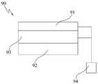
상기에서 언급된 실시예들에서, 제1 축 전도체 셀과 인접한 제2 축 전도체 셀 사이의 정전용량은 터치 위치를 검출하기 위해 측정된다. 본 발명에 따르는 전도체 패턴 구조를 갖는 정전용량식 터치 패널은, 전자 장치를 구성하기 위해, 액정 디스플레이 화면(liquid display screen)과 같은 디스플레이와 결합할 수 있다. 본 발명의 정전용량식 터치 패널을 갖는 전자 장치(90)가 도 24에서 도시된다. 전자 장치(90)는 그 위의 터치 동작을 감지하여 상응하는 터치 감지 신호들을 발생시키기 위한 정전용량식 터치 패널(91); 상기 터치 감지 신호들을 수신하여 프로세싱하고 상응하는 디스플레이 지시 신호들을 발생시키기 위한 프로세서(94); 및 상기 디스플레이 지시 신호들을 수신하여 상응하는 이미지들을 디스플레이하기 위한 디스플레이(92);를 포함한다. 정전용량식 터치 패널(91)을 디스플레이(92)와 결합시키기 위해 정전용량식 터치 패널(91)과 디스플레이(92) 사이에 접착층(adhesive layer, 93)이 배치된다.
In the above-mentioned embodiments, the capacitance between the first axis conductor cell and the adjacent second axis conductor cell is measured to detect the touch position. A capacitive touch panel having a conductor pattern structure according to the present invention can be combined with a display such as a liquid display screen to form an electronic device. An
터치 패널(91)은 디스플레이(92) 상에 배치될 수 있다. 보통, 디스플레이는 상부 기판, 하부 기판, 상부 기판과 하부 기판 사이에 배치되는 픽셀 유닛(pixel unit) 및 빛을 차단하기 위한 복수의 블랙 매트릭스들(black matrixes)을 갖는 차단층(blocking layer)를 포함한다. 바람직하게는, 본 발명의 터치 감지 회로의 제2 전도성 라인들은 터치 패널(91)의 빛 투과율을 향상시키기 위해 블랙 매트릭스들에 맞춰 조절될 수 있다.
The
본 발명의 전도체 패턴 구조는 또한 예를 들어 하부 기판의 상면(upper face) 또는 상부 기판의 하면(lower face)에 배치되어 디스플레이에 사용될 수 있다. 이러한 경우에, 상부 기판 또는 하부 기판은 또한 전도체 패턴 구조가 그 위에 형성될 수 있는 기판으로 사용될 수 있다. 본 발명의 전도체 패턴 구조가 디스플레이 패널에서 사용될 때, 제2 축 전도 라인은 빛을 차단하기 위한 다수의 블랙 매트릭스들을 포함하는 차단층과 함께 적층될 수 있다. 대안적인 실시예에서, 차단층은 생략될 수 있고, 디스플레이에서 빛을 차단하기 위한 차단 소자로 제2 축 전도 라인이 사용된다. 또한, 제2 축 전도 라인들이 금속으로 구성되는 경우에, 제2 축 전도체 셀들과 제2 축 신호 전송 라인들 사이의 저항이 효과적으로 감소될 수 있고, 따라서 제2 축 전도체 셀들과 제2 축 신호 전송 라인들 사이의 신호 전송의 감도(sensitivity)가 향상될 수 있다.
The conductor pattern structure of the present invention can also be disposed on, for example, an upper face of a lower substrate or a lower face of an upper substrate to be used for a display. In this case, the upper substrate or the lower substrate can also be used as a substrate on which a conductor pattern structure can be formed. When the conductor pattern structure of the present invention is used in a display panel, the second axis conduction line may be laminated with a barrier layer comprising a plurality of black matrices for blocking light. In an alternative embodiment, the barrier layer may be omitted and a second axis conduction line is used as a blocking element for blocking light in the display. Also, in the case where the second axis conductive lines are made of metal, the resistance between the second axis conductor cells and the second axis signal transmission lines can be effectively reduced, so that the second axis conductor cells and the second axis signal transmission The sensitivity of signal transmission between the lines can be improved.
비록 본 발명이 그의 바람직한 실시예들을 참조하여 설명되었지만, 첨부된 청구항들에 의해 정의하고자 하는 본 발명의 사상에서 벗어나지 않으며 다양한 수정 및 변경이 이루어질 수 있음이 당업자들에게 명백하다.Although the invention has been described with reference to its preferred embodiments, it will be apparent to those skilled in the art that various modifications and changes can be made without departing from the spirit of the invention as defined by the appended claims.
Claims (31)
Translated fromKorean제1 축을 따라 상기 강성 기판의 표면 상에 배열되는 복수의 제1 축 전도체 셀들을 각각 포함하는 복수의 제1 축 전도체 어셈블리들;
각각 각각의 제1 축 전도체 어셈블리의 상기 제1 축 전도체 셀들이 서로 전기적으로 연결되도록 각각의 제1 전도체 어셈블리의 인접한 제1 축 전도체 셀들 사이를 각각 연결하는 복수의 제1 축 전도 라인들;
제2 축을 따라 상기 강성 기판의 표면 상에 배열되는 복수의 제2 축 전도체 셀들을 각각 포함하는 복수의 제2 축 전도체 어셈블리들;
각각 각각의 제2 축 전도체 어셈블리의 상기 제2 축 전도체 셀들이 서로 전기적으로 연결되도록 각각의 제2 축 전도체 어셈블리의 인접한 제2 축 전도체 셀들 사이를 각각 연결하는 복수의 제2 축 전도 라인들;
상기 제1 축 전도성 어셈블리들 및 상기 제2 축 전도성 어셈블리들 사이의 전자적 연결을 절연하기 위한 복수의 절연체;
를 포함하는 터치 패널의 전도체 패턴 구조로서,
각각의 상기 제2 축 전도 라인들은 각각 상기 인접한 제1 축 전도체 셀의 적어도 일부분 위에 위치하며, 각각의 상기 절연체는 그들 사이의 전자적 연결을 절연하기 위해 상기 제2 축 전도 라인과 상기 인접한 제1 축 전도체 셀 사이에 배치되고;
상기 복수의 제1 축 전도체 셀들의 제1 셀과 상기 복수의 제2 축 전도체 셀들의 제2 셀 사이의 정전용량이 터치 위치를 검출하기 위해 측정되며;
상기 전도체 패턴 구조는 디스플레이 패널 상에 배치될 수 있고 상기 디스플레이 상에 보여지는 형상들(figures)은 상기 전도체 패턴 구조를 통해 보이는 것을 특징으로 하는 정전용량식 터치 패널의 전도체 패턴 구조.
Rigid substrates;
A plurality of first axis conductor assemblies each comprising a plurality of first axis conductor cells arranged on a surface of the rigid substrate along a first axis;
A plurality of first axial conductor lines each connecting between adjacent first axial conductor cells of each first conductor assembly such that the first axial conductor cells of each first axial conductor assembly are electrically connected to each other;
A plurality of second axis conductor assemblies each comprising a plurality of second axis conductor cells arranged on a surface of the rigid substrate along a second axis;
A plurality of second axis conductor lines each connecting between adjacent second axis conductor cells of each second axis conductor assembly such that the second axis conductor cells of each second axis conductor assembly are electrically connected to each other;
A plurality of insulators for insulating electronic connections between the first axial conductive assemblies and the second axial conductive assemblies;
As a conductor pattern structure of the touch panel comprising:
Each of the second axial conducting lines is respectively located over at least a portion of the adjacent first axial conductor cell, and each of the insulators separates the second axial conducting line and the adjacent first axial to insulate an electrical connection therebetween. Disposed between the conductor cells;
Capacitance between the first cell of the plurality of first axial conductor cells and the second cell of the plurality of second axial conductor cells is measured to detect a touch position;
The conductor pattern structure may be disposed on a display panel and the figures shown on the display are visible through the conductor pattern structure.
각각 상기 복수의 절연체들 상에 배치되는 복수의 전기적 연결 소자들을 더 포함하는 것을 특징으로 하는 정전용량식 터치 패널의 전도체 패턴 구조.
The method according to claim 1,
And a plurality of electrical connection elements disposed on the plurality of insulators, respectively.
각각의 상기 제2 축 전도 라인들은 상기 인접한 제2 축 전도체 셀들을 연결하는 적어도 2개의 분리된 브랜치들(branches)을 포함하고,
상기 브랜치들은 상기 전기적 연결 소자들을 통한 연결에 의해 서로 전자적으로 연결되는 것을 특징으로 하는 정전용량식 터치 패널의 전도체 패턴 구조.
The method according to claim 2,
Each of the second axial conducting lines comprises at least two separate branches connecting the adjacent second axial conductor cells,
And the branches are electronically connected to each other by a connection through the electrical connection elements.
상기 제2 축 전도 라인들의 적어도 2개는 상기 인접한 제2 축 전도체 셀들에 연결되는 것을 특징으로 하는 정전용량식 터치 패널의 전도체 패턴 구조.
The method according to claim 1,
At least two of the second axial conducting lines are connected to the adjacent second axial conductor cells.
상기 적어도 2개의 제2 축 전도 라인들은 동일한 인접한 제1 축 전도체 셀 위에 위치되고, 상기 인접한 제1 축 전도 라인들에 인접하는 것을 특징으로 하는 정전용량식 터치 패널의 전도체 패턴 구조.
The method of claim 4,
And said at least two second axial conducting lines are located on the same adjacent first axial conductor cell and adjacent said adjacent first axial conducting lines.
상기 제2 축 전도 라인들의 상기 적어도 2개는 서로 다른 인접한 제1 축 전도체 셀들 위에 위치되고 상기 인접한 제1 축 전도 라인은 상기 2개의 제2 축 전도 라인들 사이에 있는 것을 특징으로 하는 정전용량식 터치 패널의 전도체 패턴 구조.
The method of claim 4,
Wherein said at least two of said second axial conducting lines are located above different adjacent first axial conductor cells and said adjacent first axial conducting line is between said two second axial conducting lines. Conductor pattern structure of touch panel.
각각의 상기 제2 축 전도 라인들은 상기 인접한 제2 축 전도체 셀들의 적어도 일부분 위에 위치되는 것을 특징으로 하는 정전용량식 터치 패널의 전도체 패턴 구조.
The method according to claim 1,
Each of the second axial conductive lines is positioned over at least a portion of the adjacent second axial conductor cells.
상기 제1 축 전도 라인들 및 상기 제2 축 전도 라인들은 서로 교차하지 않는 것을 특징으로 하는 정전용량식 터치 패널의 전도체 패턴 구조.
The method according to claim 1,
And wherein the first and second axis conduction lines do not intersect each other.
상기 제1 축 전도체 셀들 및 상기 제2 축 전도체 셀들은 투명 전도성 물질로 구성되는 것을 특징으로 하는 정전용량식 터치 패널의 전도체 패턴 구조.
The method according to claim 1,
And the first axial conductor cells and the second axial conductor cells are made of a transparent conductive material.
상기 강성 기판의 상기 표면 상에 형성되는 복수의 제1 축 신호 전송 라인들 및 복수의 제2 축 신호 전송 라인들을 더 포함하되,
각각 각각의 제1 축 신호 전송 라인은 각각의 제1 축 전도체 어셈블리에 각각 연결되고 각각의 제2 축 신호 전송 라인은 각각의 제2 축 전도체 어셈블리에 연결되는 것을 특징으로 하는 정전용량식 터치 패널의 전도체 패턴 구조.
The method according to claim 1,
Further comprising a plurality of first axis signal transmission lines and a plurality of second axis signal transmission lines formed on the surface of the rigid substrate,
Each of the first axis signal transmission lines is respectively connected to a respective first axis conductor assembly and each second axis signal transmission line is connected to each of the second axis conductor assemblies. Conductor pattern structure.
제1 축을 따라 상기 기판의 표면 상에 배열되는 복수의 제1 축 전도체 셀들을 각각 포함하는 복수의 제1 축 전도체 어셈블리들;
각각 각각의 제1 축 전도체 어셈블리의 상기 제1 축 전도체 셀들이 서로 전기적으로 연결되도록 각각의 제1 축 전도체 어셈블리의 인접한 제1 축 전도체 셀들 사이를 각각 연결하는 복수의 제1 축 전도 라인들;
제2 축을 따라 상기 기판의 상기 표면 상에 배열되는 복수의 제2 축 전도체 셀들을 각각 포함하는 복수의 제2 축 전도체 어셈블리들;
각각 상기 제1 축 전도체 셀들 중의 하나 옆에 각각 설치되는 복수의 전기적 연결 소자들;
각각 각각의 제2 축 전도체 어셈블리의 상기 제2 축 전도체 셀들이 서로 전기적으로 연결되도록, 상기 전기적 연결 소자를 통한 연결에 의해 인접한 제2 전도체 셀들 사이를 각각 연결하며, 상기 인접한 제2 축 전도체 셀들을 연결하는 적어도 2개의 분리된 브랜치들을 각각 포함하고, 상기 브랜치들은 상기 전기적 연결 소자들을 통한 연결에 의해 서로 전자적으로 연결되는, 복수의 제2 축 전도 라인들; 및
상기 제1 축 전도성 어셈블리들과 상기 제2 축 전도성 어셈블리들 사이의 전자적 연결을 절연하기 위한 복수의 절연체;
를 포함하는 터치 패널의 전도체 패턴 구조로서,
각각의 상기 절연체들은 그들 사이의 전자적 연결을 절연하기 위해 상기 전기적 연결 소자와 상기 인접한 제1 축 전도 라인 사이에 배치되며;
상기 전도체 패턴 구조는 디스플레이 패널 상에 배치될 수 있고 상기 디스플레이 상에 보여지는 형상들은 상기 전도체 패턴 구조를 통해 보이는 것을 특징으로 하는 정전용량식 터치 패널의 전도체 패턴 구조.
Board;
A plurality of first axis conductor assemblies each comprising a plurality of first axis conductor cells arranged on a surface of the substrate along a first axis;
A plurality of first axial conductor lines each connecting between adjacent first axial conductor cells of each first axial conductor assembly such that the first axial conductor cells of each first axial conductor assembly are electrically connected to each other;
A plurality of second axis conductor assemblies each comprising a plurality of second axis conductor cells arranged on the surface of the substrate along a second axis;
A plurality of electrical connection elements each installed next to one of the first axial conductor cells;
Respectively connecting between adjacent second conductor cells by a connection through the electrical connection element such that the second axis conductor cells of each second axis conductor assembly are electrically connected to each other. A plurality of second axial conducting lines, each comprising at least two separate branches for connecting, wherein the branches are electronically connected to each other by a connection via the electrical connecting elements; And
A plurality of insulators for insulating electronic connections between the first axial conductive assemblies and the second axial conductive assemblies;
As a conductor pattern structure of the touch panel comprising:
Each of the insulators is disposed between the electrical connection element and the adjacent first axial conducting line to insulate the electrical connection there between;
The conductor pattern structure may be disposed on a display panel and the shapes shown on the display are seen through the conductor pattern structure.
상기 제2 축 전도 라인들의 적어도 2개는 상기 인접한 제2 축 전도체 셀들에 연결되는 것을 특징으로 하는 정전용량식 터치 패널의 전도체 패턴 구조.
The method of claim 12,
At least two of the second axial conducting lines are connected to the adjacent second axial conductor cells.
상기 적어도 2개의 제2 축 전도 라인들은 동일한 인접한 전기적 연결 소자들 위에 위치되는 것을 특징으로 하는 정전용량식 터치 패널의 전도체 패턴 구조.
The method according to claim 13,
And the at least two second axial conducting lines are positioned over the same adjacent electrically connecting elements.
상기 제2 축 전도 라인들의 상기 적어도 2개는 서로 다른 인접한 전기적 연결 소자 위에 위치되고 상기 인접한 제1 축 전도 라인은 상기 제2 축 전도 라인들 사이에 있는 것을 특징으로 하는 정전용량식 터치 패널의 전도체 패턴 구조.
The method according to claim 13,
The at least two of the second axial conducting lines are positioned over different adjacent electrically connecting elements and the adjacent first axial conducting line is between the second axial conducting lines. Pattern structure.
상기 제1 축 전도체 셀들 및 상기 제2 축 전도체 셀들은 투명 전도성 물질로 구성되는 것을 특징으로 하는 정전용량식 터치 패널의 전도체 패턴 구조.
The method of claim 12,
And the first axial conductor cells and the second axial conductor cells are made of a transparent conductive material.
상기 복수의 제1 축 전도체 셀들의 제1 셀과 상기 복수의 제2 축 전도체 셀들 사이의 제2 셀 사이의 정전용량이 터치 위치를 검출하기 위해 측정되는 것을 특징으로 하는 정전용량식 터치 패널의 전도체 패턴 구조.
The method of claim 12,
A capacitance between a first cell of the plurality of first axial conductor cells and a second cell between the plurality of second axial conductor cells is measured to detect a touch position. Pattern structure.
상기 기판은 강성 기판인 것을 특징으로 하는 정전용량식 터치 패널의 전도체 패턴 구조.
The method of claim 12,
The substrate is a conductive pattern structure of the capacitive touch panel, characterized in that the rigid substrate.
상기 기판의 상기 표면 상에 형성되는 복수의 제1 축 신호 전송 라인들 및 복수의 제2 축 신호 전송 라인들을 더 포함하며,
각각 각각의 제1 축 신호 전송 라인은 각각의 제1 축 전도체 어셈블리에 연결되고 각각의 제2 축 신호 전송 라인은 각각의 제2 축 전도체 어셈블리에 연결되는 것을 특징으로 하는 정전용량식 터치 패널의 전도체 패턴 구조.
The method of claim 12,
A plurality of first axis signal transmission lines and a plurality of second axis signal transmission lines formed on the surface of the substrate,
Each of the first axis signal transmission lines is connected to a respective first axis conductor assembly and each second axis signal transmission line is connected to each of the second axis conductor assemblies. Pattern structure.
제1 축을 따라 상기 기판의 표면 상에 배열되는 복수의 제1 축 전도체 셀들을 각각 포함하되, 각각의 제1 축 전도체 셀은 윈도우(window)를 포함하는, 복수의 제1 축 전도체 어셈블리들;
각각의 제1 축 전도체 어셈블리의 상기 제1 축 전도체 셀들이 서로 전기적으로 연결되도록 각각의 제1 축 전도체 어셈블리의 인접한 제1 축 전도체 셀들 사이를 각각 연결하는 복수의 제1 축 전도 라인들;
제2 축을 따라 상기 기판의 상기 표면 상에 배열되는 복수의 제2 축 전도체 셀들을 각각 포함하는 복수의 제2 축 전도체 어셈블리들;
상기 제1 축 전도체 셀의 상기 윈도우에 각각 설치되는 복수의 전기적 연결 소자들;
각각 각각의 제2 축 전도체 어셈블리의 상기 제2 축 전도체 셀들이 서로 전기적으로 연결되도록, 상기 전기적 연결 소자를 통한 연결에 의해 인접한 제2 축 전도체 셀들 사이를 각각 연결하며, 상기 인접한 제2 축 전도체 셀들을 연결하는 적어도 2개의 분리된 브랜치들을 각각 포함하고, 상기 브랜치들은 상기 전기적 연결 소자들을 통한 연결에 의해 서로 전자적으로 연결되는, 복수의 제2 축 전도 라인들; 및
상기 제1 축 전도성 어셈블리들과 상기 제2 축 전도성 어셈블리들 사이의 전자적 연결을 절연하기 위한 복수의 절연체;
를 포함하는 터치 패널의 전도체 패턴 구조로서,
각각의 상기 제2 축 전도 라인들은 각각 상기 인접한 제1 축 전도체 셀의 적어도 일부분 위에 위치하고, 각각의 상기 절연체는 그들 사이의 전자적 연결을 절연하기 위해 상기 제2 축 전도 라인과 상기 인접한 제1 축 전도체 셀들 사이에 배치되며;
상기 전도체 패턴 구조는 디스플레이 패널 상에 배치될 수 있고 상기 디스플레이 상에 보여지는 형상들은 상기 전도체 패턴 구조를 통해 보이는 것을 특징으로 하는 정전용량식 터치 패널의 전도체 패턴 구조.
Board;
A plurality of first axial conductor assemblies each comprising a plurality of first axial conductor cells arranged on a surface of the substrate along a first axis, wherein each first axial conductor cell comprises a window;
A plurality of first axial conductor lines each connecting between adjacent first axial conductor cells of each first axial conductor assembly such that the first axial conductor cells of each first axial conductor assembly are electrically connected to each other;
A plurality of second axis conductor assemblies each comprising a plurality of second axis conductor cells arranged on the surface of the substrate along a second axis;
A plurality of electrical connection elements respectively installed in the window of the first axial conductor cell;
Each connecting between adjacent second axis conductor cells by a connection via the electrical connection element such that the second axis conductor cells of each second axis conductor assembly are electrically connected to each other, the adjacent second axis conductor cells A plurality of second axial conducting lines, each of which includes at least two separate branches for connecting the two branches; And
A plurality of insulators for insulating electronic connections between the first axial conductive assemblies and the second axial conductive assemblies;
As a conductor pattern structure of the touch panel comprising:
Each of the second axial conductor lines is respectively located over at least a portion of the adjacent first axial conductor cell, and each of the insulators is adapted to insulate the electrical connection therebetween with the second axial conductor line and the adjacent first axial conductor. Disposed between cells;
The conductor pattern structure may be disposed on a display panel and the shapes shown on the display are seen through the conductor pattern structure.
상기 제2 축 전도 라인들의 적어도 2개는 상기 인접한 제2 축 전도체 셀들에 연결되는 것을 특징으로 하는 정전용량식 터치 패널의 전도체 패턴 구조.
23. The method of claim 21,
At least two of the second axial conducting lines are connected to the adjacent second axial conductor cells.
상기 적어도 2개의 제2 축 전도 라인들은 동일한 인접한 제1 축 전도체 셀 위에 위치되고, 상기 인접한 제1 축 전도 라인에 인접하는 것을 특징으로 하는 정전용량식 터치 패널의 전도체 패턴 구조.
23. The method of claim 22,
And the at least two second axial conducting lines are located on the same adjacent first axial conductor cell and adjacent to the adjacent first axial conducting line.
상기 적어도 2개의 제2 축 전도 라인들은 서로 다른 인접한 제1 축 전도체 셀들 위에 위치하고 상기 인접한 제1 축 전도 라인은 상기 2개의 제2 축 전도 라인들 사이에 있는 것을 특징으로 하는 정전용량식 터치 패널의 전도체 패턴 구조.
24. The method of claim 23,
Wherein the at least two second axial conducting lines are positioned over different adjacent first axial conductor cells and the adjacent first axial conducting line is between the two second axial conducting lines. Conductor pattern structure.
상기 제1 축 전도체 셀들 및 상기 제2 축 전도체 셀들은 투명 전도성 물질로 구성되는 것을 특징으로 하는 정전용량식 터치 패널의 전도체 패턴 구조.
23. The method of claim 21,
And the first axial conductor cells and the second axial conductor cells are made of a transparent conductive material.
상기 복수의 제1 축 전도체 셀들의 제1 셀과 상기 복수의 제2 축 전도체 셀들의 제2 셀 사이의 정전용량이 터치 위치를 검출하기 위해 측정되는 것을 특징으로 하는 정전용량식 터치 패널의 전도체 패턴 구조.
23. The method of claim 21,
The capacitance pattern between the first cell of the plurality of first axial conductor cells and the second cell of the plurality of second axial conductor cells is measured to detect a touch position. rescue.
상기 기판은 강성 기판인 것을 특징으로 하는 정전용량식 터치 패널의 전도체 패턴 구조.
23. The method of claim 21,
The substrate is a conductive pattern structure of the capacitive touch panel, characterized in that the rigid substrate.
상기 강성 기판의 상기 표면 상에 형성되는 복수의 제1 축 신호 전송 라인들 및 복수의 제2 축 신호 전송 라인들을 더 포함하며,
각각의 제1 축 신호 전송 라인은 각각의 제1 축 전도체 어셈블리에 각각 연결되고 각각의 제2 축 신호 전송 라인은 각각의 제2 축 전도체 어셈블리에 각각 연결되는 것을 특징으로 하는 정전용량식 터치 패널의 전도체 패턴 구조.
23. The method of claim 21,
A plurality of first axis signal transmission lines and a plurality of second axis signal transmission lines formed on the surface of the rigid substrate,
Wherein each first axis signal transmission line is respectively connected to each first axis conductor assembly and each second axis signal transmission line is respectively connected to each second axis conductor assembly. Conductor pattern structure.
상기 제1 축 전도체 셀과 상기 윈도우 내의 상기 전기적 연결 소자 사이에 갭(gap)이 있어서 그것들이 전자적으로 연결되지 않는 것을 특징으로 하는 정전용량식 터치 패널의 전도체 패턴 구조.
23. The method of claim 21,
And a gap between the first axial conductor cell and the electrical connection element in the window so that they are not electronically connected.
상기 윈도우 및 상기 전자적 연결 소자는 모두 기하학적 형태의 윤곽을 갖는 것을 특징으로 하는 정전용량식 터치 패널의 전도체 패턴 구조.23. The method of claim 21,
The window and the electronic connection element both have a contour of the geometric shape of the conductor pattern structure of the capacitive touch panel.
Applications Claiming Priority (2)
| Application Number | Priority Date | Filing Date | Title |
|---|---|---|---|
| US13/444,849US8610689B2 (en) | 2007-04-27 | 2012-04-12 | Conductor pattern structure of capacitive touch panel |
| US13/444,849 | 2012-04-12 |
Related Child Applications (1)
| Application Number | Title | Priority Date | Filing Date |
|---|---|---|---|
| KR1020130128741ADivisionKR101438096B1 (en) | 2012-04-12 | 2013-10-28 | Conductor pattern structure of capacitive touch panel |
Publications (2)
| Publication Number | Publication Date |
|---|---|
| KR20130116138A KR20130116138A (en) | 2013-10-23 |
| KR101389086B1true KR101389086B1 (en) | 2014-04-25 |
Family
ID=46146638
Family Applications (2)
| Application Number | Title | Priority Date | Filing Date |
|---|---|---|---|
| KR1020120039545AActiveKR101389086B1 (en) | 2012-04-12 | 2012-04-17 | Conductor pattern structure of capacitive touch panel |
| KR1020130128741AActiveKR101438096B1 (en) | 2012-04-12 | 2013-10-28 | Conductor pattern structure of capacitive touch panel |
Family Applications After (1)
| Application Number | Title | Priority Date | Filing Date |
|---|---|---|---|
| KR1020130128741AActiveKR101438096B1 (en) | 2012-04-12 | 2013-10-28 | Conductor pattern structure of capacitive touch panel |
Country Status (4)
| Country | Link |
|---|---|
| EP (2) | EP2650765B1 (en) |
| JP (1) | JP5877864B2 (en) |
| KR (2) | KR101389086B1 (en) |
| TW (2) | TWI423105B (en) |
Families Citing this family (10)
| Publication number | Priority date | Publication date | Assignee | Title |
|---|---|---|---|---|
| CN103294272B (en)* | 2013-05-30 | 2016-04-13 | 南昌欧菲光科技有限公司 | Nesa coating |
| US9439302B2 (en) | 2013-05-30 | 2016-09-06 | Nanchang O-Film Tech Co., Ltd. | Transparent conductive film |
| CN105718092B (en)* | 2014-12-01 | 2018-10-26 | 宸鸿科技(厦门)有限公司 | Touch panel |
| US9703439B2 (en) | 2014-12-26 | 2017-07-11 | Lg Display Co., Ltd. | Touch sensor integrated type display device |
| JP6396815B2 (en)* | 2015-01-29 | 2018-09-26 | アルプス電気株式会社 | Input device |
| CN104932764B (en)* | 2015-06-25 | 2017-12-08 | 京东方科技集团股份有限公司 | A kind of capacitance type touch control screen and preparation method thereof, display device |
| KR102146460B1 (en)* | 2015-12-08 | 2020-08-20 | 동우 화인켐 주식회사 | Touch sensor and display device comprising the same |
| KR102756220B1 (en)* | 2016-12-28 | 2025-01-17 | 엘지디스플레이 주식회사 | Display device |
| CN106951131B (en)* | 2017-02-23 | 2020-09-18 | 深圳市骏达光电股份有限公司 | Touch screen |
| KR102551226B1 (en)* | 2018-07-25 | 2023-07-04 | 삼성디스플레이 주식회사 | Touch member and display device with the same |
Citations (4)
| Publication number | Priority date | Publication date | Assignee | Title |
|---|---|---|---|---|
| JP2010231288A (en) | 2009-03-26 | 2010-10-14 | Seiko Epson Corp | Touch panel, manufacturing method thereof, display device, and electronic device |
| JP2010244120A (en) | 2009-04-01 | 2010-10-28 | Seiko Epson Corp | Touch panel manufacturing method, display device manufacturing method, and electronic device manufacturing method |
| KR101040881B1 (en)* | 2010-04-12 | 2011-06-16 | 삼성모바일디스플레이주식회사 | Touch screen panel |
| KR101073333B1 (en)* | 2009-08-27 | 2011-10-12 | 삼성모바일디스플레이주식회사 | Touch Screen Panel and fabrication method thereof |
Family Cites Families (23)
| Publication number | Priority date | Publication date | Assignee | Title |
|---|---|---|---|---|
| US4233522A (en) | 1978-10-30 | 1980-11-11 | General Electric Company | Capacitive touch switch array |
| US4733222A (en) | 1983-12-27 | 1988-03-22 | Integrated Touch Arrays, Inc. | Capacitance-variation-sensitive touch sensing array system |
| US5459463A (en) | 1990-05-25 | 1995-10-17 | Sextant Avionique | Device for locating an object situated close to a detection area and a transparent keyboard using said device |
| US5880411A (en) | 1992-06-08 | 1999-03-09 | Synaptics, Incorporated | Object position detector with edge motion feature and gesture recognition |
| DE69324067T2 (en) | 1992-06-08 | 1999-07-15 | Synaptics Inc | Object position detector |
| US5847690A (en) | 1995-10-24 | 1998-12-08 | Lucent Technologies Inc. | Integrated liquid crystal display and digitizer having a black matrix layer adapted for sensing screen touch location |
| US6188391B1 (en)* | 1998-07-09 | 2001-02-13 | Synaptics, Inc. | Two-layer capacitive touchpad and method of making same |
| US7030860B1 (en) | 1999-10-08 | 2006-04-18 | Synaptics Incorporated | Flexible transparent touch sensing system for electronic devices |
| US6498590B1 (en) | 2001-05-24 | 2002-12-24 | Mitsubishi Electric Research Laboratories, Inc. | Multi-user touch surface |
| US6970160B2 (en)* | 2002-12-19 | 2005-11-29 | 3M Innovative Properties Company | Lattice touch-sensing system |
| US20050030048A1 (en)* | 2003-08-05 | 2005-02-10 | Bolender Robert J. | Capacitive sensing device for use in a keypad assembly |
| TW200842681A (en)* | 2007-04-27 | 2008-11-01 | Tpk Touch Solutions Inc | Touch pattern structure of a capacitive touch panel |
| TW200901014A (en)* | 2007-06-28 | 2009-01-01 | Sense Pad Tech Co Ltd | Touch panel device |
| TWM344544U (en)* | 2007-12-25 | 2008-11-11 | Cando Corp | Sensory structure of touch panel |
| US8711105B2 (en)* | 2008-08-21 | 2014-04-29 | Wacom Co., Ltd. | Touchscreen with extended conductive pattern |
| US8493337B2 (en)* | 2008-09-22 | 2013-07-23 | Ritfast Corporation | Light transmission touch panel |
| TWI436256B (en)* | 2008-11-07 | 2014-05-01 | Focaltech Systems Ltd | Mutual capacitive touchpad and modular mutual capacitive touchpad |
| TWI427520B (en)* | 2009-12-10 | 2014-02-21 | Au Optronics Corp | Touch-sensing display panel and touch-sensing substrate |
| KR101100987B1 (en)* | 2010-03-23 | 2011-12-30 | 삼성모바일디스플레이주식회사 | Touch screen panel |
| KR101691619B1 (en)* | 2010-09-14 | 2017-01-02 | 삼성디스플레이 주식회사 | Touch Screen Panel and Display Device Having the Same |
| JP5871530B2 (en)* | 2010-09-30 | 2016-03-01 | セイコーインスツル株式会社 | Display device with touch panel |
| KR101448251B1 (en)* | 2010-10-28 | 2014-10-08 | 삼성디스플레이 주식회사 | Touch Screen Panel and Display Device Having the Same |
| CN102799301B (en)* | 2011-05-28 | 2015-05-20 | 宸鸿科技(厦门)有限公司 | Electrode structure of touch panel, manufacturing method and touch panel |
- 2012
- 2012-04-17KRKR1020120039545Apatent/KR101389086B1/enactiveActive
- 2012-05-04EPEP12166895.8Apatent/EP2650765B1/enactiveActive
- 2012-05-04EPEP13186412.6Apatent/EP2687962B1/enactiveActive
- 2013
- 2013-01-28TWTW102103061Apatent/TWI423105B/enactive
- 2013-01-28TWTW102201808Upatent/TWM453197U/ennot_activeIP Right Cessation
- 2013-10-28KRKR1020130128741Apatent/KR101438096B1/enactiveActive
- 2014
- 2014-03-26JPJP2014063548Apatent/JP5877864B2/enactiveActive
Patent Citations (4)
| Publication number | Priority date | Publication date | Assignee | Title |
|---|---|---|---|---|
| JP2010231288A (en) | 2009-03-26 | 2010-10-14 | Seiko Epson Corp | Touch panel, manufacturing method thereof, display device, and electronic device |
| JP2010244120A (en) | 2009-04-01 | 2010-10-28 | Seiko Epson Corp | Touch panel manufacturing method, display device manufacturing method, and electronic device manufacturing method |
| KR101073333B1 (en)* | 2009-08-27 | 2011-10-12 | 삼성모바일디스플레이주식회사 | Touch Screen Panel and fabrication method thereof |
| KR101040881B1 (en)* | 2010-04-12 | 2011-06-16 | 삼성모바일디스플레이주식회사 | Touch screen panel |
Also Published As
| Publication number | Publication date |
|---|---|
| TWI423105B (en) | 2014-01-11 |
| EP2650765B1 (en) | 2016-03-02 |
| KR101438096B1 (en) | 2014-09-12 |
| TW201342179A (en) | 2013-10-16 |
| JP5877864B2 (en) | 2016-03-08 |
| JP2014157611A (en) | 2014-08-28 |
| KR20130116138A (en) | 2013-10-23 |
| EP2687962A1 (en) | 2014-01-22 |
| TWM453197U (en) | 2013-05-11 |
| KR20130136417A (en) | 2013-12-12 |
| EP2687962B1 (en) | 2017-04-12 |
| EP2650765A2 (en) | 2013-10-16 |
| EP2650765A3 (en) | 2014-04-23 |
Similar Documents
| Publication | Publication Date | Title |
|---|---|---|
| US8610689B2 (en) | Conductor pattern structure of capacitive touch panel | |
| KR101389086B1 (en) | Conductor pattern structure of capacitive touch panel | |
| EP2336862A2 (en) | Conductor pattern structure of capacitive touch panel | |
| US9454267B2 (en) | Touch sensing circuit and method for making the same | |
| US8605050B2 (en) | Conductor pattern structure of capacitive touch panel | |
| KR101379376B1 (en) | Conductor pattern structure of capacitive touch panel | |
| CN102830869B (en) | Conductive pattern structure of capacitive touch panel | |
| CN202795317U (en) | Conductive pattern structure of capacitive touch panel |
Legal Events
| Date | Code | Title | Description |
|---|---|---|---|
| A201 | Request for examination | ||
| PA0109 | Patent application | Patent event code:PA01091R01D Comment text:Patent Application Patent event date:20120417 | |
| PA0201 | Request for examination | ||
| E902 | Notification of reason for refusal | ||
| PE0902 | Notice of grounds for rejection | Comment text:Notification of reason for refusal Patent event date:20130826 Patent event code:PE09021S01D | |
| PG1501 | Laying open of application | ||
| A107 | Divisional application of patent | ||
| PA0107 | Divisional application | Comment text:Divisional Application of Patent Patent event date:20131028 Patent event code:PA01071R01D | |
| E701 | Decision to grant or registration of patent right | ||
| PE0701 | Decision of registration | Patent event code:PE07011S01D Comment text:Decision to Grant Registration Patent event date:20140122 | |
| GRNT | Written decision to grant | ||
| PR0701 | Registration of establishment | Comment text:Registration of Establishment Patent event date:20140418 Patent event code:PR07011E01D | |
| PR1002 | Payment of registration fee | Payment date:20140421 End annual number:3 Start annual number:1 | |
| PG1601 | Publication of registration | ||
| FPAY | Annual fee payment | Payment date:20170223 Year of fee payment:4 | |
| PR1001 | Payment of annual fee | Payment date:20170223 Start annual number:4 End annual number:4 | |
| FPAY | Annual fee payment | Payment date:20180208 Year of fee payment:5 | |
| PR1001 | Payment of annual fee | Payment date:20180208 Start annual number:5 End annual number:5 | |
| FPAY | Annual fee payment | Payment date:20190227 Year of fee payment:6 | |
| PR1001 | Payment of annual fee | Payment date:20190227 Start annual number:6 End annual number:6 | |
| FPAY | Annual fee payment | Payment date:20200220 Year of fee payment:7 | |
| PR1001 | Payment of annual fee | Payment date:20200220 Start annual number:7 End annual number:7 | |
| PR1001 | Payment of annual fee | Payment date:20210324 Start annual number:8 End annual number:8 | |
| PR1001 | Payment of annual fee | Payment date:20220302 Start annual number:9 End annual number:9 | |
| PR1001 | Payment of annual fee | Payment date:20240319 Start annual number:11 End annual number:11 | |
| PR1001 | Payment of annual fee | Payment date:20250317 Start annual number:12 End annual number:12 |