KR101387877B1 - Advanced mixing system for integrated tool having site-isolated reactors - Google Patents
Advanced mixing system for integrated tool having site-isolated reactorsDownload PDFInfo
- Publication number
- KR101387877B1 KR101387877B1KR1020097013507AKR20097013507AKR101387877B1KR 101387877 B1KR101387877 B1KR 101387877B1KR 1020097013507 AKR1020097013507 AKR 1020097013507AKR 20097013507 AKR20097013507 AKR 20097013507AKR 101387877 B1KR101387877 B1KR 101387877B1
- Authority
- KR
- South Korea
- Prior art keywords
- substrate
- processing
- site
- reactor
- manifolds
- Prior art date
- Legal status (The legal status is an assumption and is not a legal conclusion. Google has not performed a legal analysis and makes no representation as to the accuracy of the status listed.)
- Expired - Fee Related
Links
Images


Classifications
- C—CHEMISTRY; METALLURGY
- C23—COATING METALLIC MATERIAL; COATING MATERIAL WITH METALLIC MATERIAL; CHEMICAL SURFACE TREATMENT; DIFFUSION TREATMENT OF METALLIC MATERIAL; COATING BY VACUUM EVAPORATION, BY SPUTTERING, BY ION IMPLANTATION OR BY CHEMICAL VAPOUR DEPOSITION, IN GENERAL; INHIBITING CORROSION OF METALLIC MATERIAL OR INCRUSTATION IN GENERAL
- C23C—COATING METALLIC MATERIAL; COATING MATERIAL WITH METALLIC MATERIAL; SURFACE TREATMENT OF METALLIC MATERIAL BY DIFFUSION INTO THE SURFACE, BY CHEMICAL CONVERSION OR SUBSTITUTION; COATING BY VACUUM EVAPORATION, BY SPUTTERING, BY ION IMPLANTATION OR BY CHEMICAL VAPOUR DEPOSITION, IN GENERAL
- C23C16/00—Chemical coating by decomposition of gaseous compounds, without leaving reaction products of surface material in the coating, i.e. chemical vapour deposition [CVD] processes
- C23C16/44—Chemical coating by decomposition of gaseous compounds, without leaving reaction products of surface material in the coating, i.e. chemical vapour deposition [CVD] processes characterised by the method of coating
- C23C16/455—Chemical coating by decomposition of gaseous compounds, without leaving reaction products of surface material in the coating, i.e. chemical vapour deposition [CVD] processes characterised by the method of coating characterised by the method used for introducing gases into reaction chamber or for modifying gas flows in reaction chamber
- C23C16/45514—Mixing in close vicinity to the substrate
- C—CHEMISTRY; METALLURGY
- C23—COATING METALLIC MATERIAL; COATING MATERIAL WITH METALLIC MATERIAL; CHEMICAL SURFACE TREATMENT; DIFFUSION TREATMENT OF METALLIC MATERIAL; COATING BY VACUUM EVAPORATION, BY SPUTTERING, BY ION IMPLANTATION OR BY CHEMICAL VAPOUR DEPOSITION, IN GENERAL; INHIBITING CORROSION OF METALLIC MATERIAL OR INCRUSTATION IN GENERAL
- C23C—COATING METALLIC MATERIAL; COATING MATERIAL WITH METALLIC MATERIAL; SURFACE TREATMENT OF METALLIC MATERIAL BY DIFFUSION INTO THE SURFACE, BY CHEMICAL CONVERSION OR SUBSTITUTION; COATING BY VACUUM EVAPORATION, BY SPUTTERING, BY ION IMPLANTATION OR BY CHEMICAL VAPOUR DEPOSITION, IN GENERAL
- C23C16/00—Chemical coating by decomposition of gaseous compounds, without leaving reaction products of surface material in the coating, i.e. chemical vapour deposition [CVD] processes
- C23C16/44—Chemical coating by decomposition of gaseous compounds, without leaving reaction products of surface material in the coating, i.e. chemical vapour deposition [CVD] processes characterised by the method of coating
- C23C16/455—Chemical coating by decomposition of gaseous compounds, without leaving reaction products of surface material in the coating, i.e. chemical vapour deposition [CVD] processes characterised by the method of coating characterised by the method used for introducing gases into reaction chamber or for modifying gas flows in reaction chamber
- C23C16/45563—Gas nozzles
- C23C16/45574—Nozzles for more than one gas
- C—CHEMISTRY; METALLURGY
- C23—COATING METALLIC MATERIAL; COATING MATERIAL WITH METALLIC MATERIAL; CHEMICAL SURFACE TREATMENT; DIFFUSION TREATMENT OF METALLIC MATERIAL; COATING BY VACUUM EVAPORATION, BY SPUTTERING, BY ION IMPLANTATION OR BY CHEMICAL VAPOUR DEPOSITION, IN GENERAL; INHIBITING CORROSION OF METALLIC MATERIAL OR INCRUSTATION IN GENERAL
- C23C—COATING METALLIC MATERIAL; COATING MATERIAL WITH METALLIC MATERIAL; SURFACE TREATMENT OF METALLIC MATERIAL BY DIFFUSION INTO THE SURFACE, BY CHEMICAL CONVERSION OR SUBSTITUTION; COATING BY VACUUM EVAPORATION, BY SPUTTERING, BY ION IMPLANTATION OR BY CHEMICAL VAPOUR DEPOSITION, IN GENERAL
- C23C16/00—Chemical coating by decomposition of gaseous compounds, without leaving reaction products of surface material in the coating, i.e. chemical vapour deposition [CVD] processes
- C23C16/44—Chemical coating by decomposition of gaseous compounds, without leaving reaction products of surface material in the coating, i.e. chemical vapour deposition [CVD] processes characterised by the method of coating
- C23C16/52—Controlling or regulating the coating process
- H—ELECTRICITY
- H01—ELECTRIC ELEMENTS
- H01L—SEMICONDUCTOR DEVICES NOT COVERED BY CLASS H10
- H01L21/00—Processes or apparatus adapted for the manufacture or treatment of semiconductor or solid state devices or of parts thereof
- H01L21/67—Apparatus specially adapted for handling semiconductor or electric solid state devices during manufacture or treatment thereof; Apparatus specially adapted for handling wafers during manufacture or treatment of semiconductor or electric solid state devices or components ; Apparatus not specifically provided for elsewhere
- H01L21/67005—Apparatus not specifically provided for elsewhere
- H01L21/67011—Apparatus for manufacture or treatment
- H01L21/67017—Apparatus for fluid treatment
- H—ELECTRICITY
- H01—ELECTRIC ELEMENTS
- H01L—SEMICONDUCTOR DEVICES NOT COVERED BY CLASS H10
- H01L21/00—Processes or apparatus adapted for the manufacture or treatment of semiconductor or solid state devices or of parts thereof
- H01L21/67—Apparatus specially adapted for handling semiconductor or electric solid state devices during manufacture or treatment thereof; Apparatus specially adapted for handling wafers during manufacture or treatment of semiconductor or electric solid state devices or components ; Apparatus not specifically provided for elsewhere
- H01L21/67005—Apparatus not specifically provided for elsewhere
- H01L21/67242—Apparatus for monitoring, sorting or marking
- H01L21/67276—Production flow monitoring, e.g. for increasing throughput
- Y—GENERAL TAGGING OF NEW TECHNOLOGICAL DEVELOPMENTS; GENERAL TAGGING OF CROSS-SECTIONAL TECHNOLOGIES SPANNING OVER SEVERAL SECTIONS OF THE IPC; TECHNICAL SUBJECTS COVERED BY FORMER USPC CROSS-REFERENCE ART COLLECTIONS [XRACs] AND DIGESTS
- Y10—TECHNICAL SUBJECTS COVERED BY FORMER USPC
- Y10S—TECHNICAL SUBJECTS COVERED BY FORMER USPC CROSS-REFERENCE ART COLLECTIONS [XRACs] AND DIGESTS
- Y10S438/00—Semiconductor device manufacturing: process
- Y10S438/907—Continuous processing
- Y10S438/908—Utilizing cluster apparatus
- Y—GENERAL TAGGING OF NEW TECHNOLOGICAL DEVELOPMENTS; GENERAL TAGGING OF CROSS-SECTIONAL TECHNOLOGIES SPANNING OVER SEVERAL SECTIONS OF THE IPC; TECHNICAL SUBJECTS COVERED BY FORMER USPC CROSS-REFERENCE ART COLLECTIONS [XRACs] AND DIGESTS
- Y10—TECHNICAL SUBJECTS COVERED BY FORMER USPC
- Y10S—TECHNICAL SUBJECTS COVERED BY FORMER USPC CROSS-REFERENCE ART COLLECTIONS [XRACs] AND DIGESTS
- Y10S438/00—Semiconductor device manufacturing: process
- Y10S438/913—Diverse treatments performed in unitary chamber
- Y—GENERAL TAGGING OF NEW TECHNOLOGICAL DEVELOPMENTS; GENERAL TAGGING OF CROSS-SECTIONAL TECHNOLOGIES SPANNING OVER SEVERAL SECTIONS OF THE IPC; TECHNICAL SUBJECTS COVERED BY FORMER USPC CROSS-REFERENCE ART COLLECTIONS [XRACs] AND DIGESTS
- Y10—TECHNICAL SUBJECTS COVERED BY FORMER USPC
- Y10T—TECHNICAL SUBJECTS COVERED BY FORMER US CLASSIFICATION
- Y10T137/00—Fluid handling
- Y10T137/4673—Plural tanks or compartments with parallel flow
- Y10T137/469—Sequentially filled and emptied [e.g., holding type]
- Y—GENERAL TAGGING OF NEW TECHNOLOGICAL DEVELOPMENTS; GENERAL TAGGING OF CROSS-SECTIONAL TECHNOLOGIES SPANNING OVER SEVERAL SECTIONS OF THE IPC; TECHNICAL SUBJECTS COVERED BY FORMER USPC CROSS-REFERENCE ART COLLECTIONS [XRACs] AND DIGESTS
- Y10—TECHNICAL SUBJECTS COVERED BY FORMER USPC
- Y10T—TECHNICAL SUBJECTS COVERED BY FORMER US CLASSIFICATION
- Y10T137/00—Fluid handling
- Y10T137/8593—Systems
- Y10T137/87249—Multiple inlet with multiple outlet
- Y—GENERAL TAGGING OF NEW TECHNOLOGICAL DEVELOPMENTS; GENERAL TAGGING OF CROSS-SECTIONAL TECHNOLOGIES SPANNING OVER SEVERAL SECTIONS OF THE IPC; TECHNICAL SUBJECTS COVERED BY FORMER USPC CROSS-REFERENCE ART COLLECTIONS [XRACs] AND DIGESTS
- Y10—TECHNICAL SUBJECTS COVERED BY FORMER USPC
- Y10T—TECHNICAL SUBJECTS COVERED BY FORMER US CLASSIFICATION
- Y10T137/00—Fluid handling
- Y10T137/8593—Systems
- Y10T137/87265—Dividing into parallel flow paths with recombining
- Y10T137/87281—System having plural inlets
Landscapes
- Chemical & Material Sciences (AREA)
- Engineering & Computer Science (AREA)
- Organic Chemistry (AREA)
- Metallurgy (AREA)
- Mechanical Engineering (AREA)
- Materials Engineering (AREA)
- Chemical Kinetics & Catalysis (AREA)
- General Chemical & Material Sciences (AREA)
- General Physics & Mathematics (AREA)
- Power Engineering (AREA)
- Microelectronics & Electronic Packaging (AREA)
- Computer Hardware Design (AREA)
- Manufacturing & Machinery (AREA)
- Condensed Matter Physics & Semiconductors (AREA)
- Physics & Mathematics (AREA)
- Automation & Control Theory (AREA)
- Physical Or Chemical Processes And Apparatus (AREA)
- Cleaning Or Drying Semiconductors (AREA)
- Chemical Vapour Deposition (AREA)
Abstract
Translated fromKorean
Description
Translated fromKorean발명자:inventor:
Kurt H. Weiner, Tony P. Chiang, Aaron Francis and John SchmidtKurt H. Weiner, Tony P. Chiang, Aaron Francis and John Schmidt
기술분야Technical field
여기에서의 본 발명은 일반적으로 기판 처리에 관한 것이고, 특히 통합된 사이트-분리된 처리 및 풀-웨이퍼 (full-wafer) 처리를 이용한 기판 처리에 관한 것이다.The present invention relates generally to substrate processing, and more particularly to substrate processing using integrated site-separated processing and full-wafer processing.
배경background
실리콘 집적 회로 (IC) 의 각각의 연속적인 생성에 대한 원하는 성능 향상을 달성하기 위하여, 반도체 제조는 새로운 재료들과 향상된 프로세스 시퀀스로의 통합에 크게 의존되었다. 유감스럽게도, 통상의 반도체 제조 장비는 재료 조사 및 통합에 적합하지 않다. 통상의 반도체 제조 장비의 사용에 영향을 미치는 문제들은 신속히 프로세스 재료 및 화학 약품을 변경하는데 대한 어려움, 단일 반응기 또는 프로세스 챔버에서 다수의 재료나 화학 약품을 통합하고 시퀀싱하는 제한된 능력, 높은 장비 사용 비용, 큰 샘플 크기 (300㎜ 웨이퍼) 및 경직된 프로세스/반응기 구성들을 포함한다. 종래의 제조 도구를 보완하기 위하여, 폭 넓은 제조 조건에 대해 새로운 재료 및 재료 처리 시퀀스의 빠른 검사를 용이하게 하는 프로세스 장비에 대한 필요성이 커지고 있다.In order to achieve the desired performance improvements for each successive generation of silicon integrated circuits (ICs), semiconductor fabrication has relied heavily on integration of new materials and improved process sequences. Unfortunately, conventional semiconductor manufacturing equipment is not suitable for material investigation and integration. Problems affecting the use of conventional semiconductor manufacturing equipment include the difficulty of rapidly changing process materials and chemicals, limited ability to integrate and sequence multiple materials or chemicals in a single reactor or process chamber, high equipment usage costs, Large sample size (300 mm wafer) and rigid process / reactor configurations. To complement conventional manufacturing tools, there is a growing need for process equipment that facilitates the quick inspection of new materials and material processing sequences over a wide range of manufacturing conditions.
도면의 간단한 설명Brief Description of Drawings
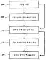
도 1 은 일 실시형태 하에서, 기판 처리 시스템 (SPS: substrate processing system) 이다.1 is a substrate processing system (SPS), under one embodiment.
도 2 는 일 실시형태 하에서, 조합형 프로세스 시퀀스 통합에 대한 흐름도이다.2 is a flow diagram for combined process sequence integration, under one embodiment.
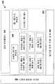
도 3 은 일 실시형태 하에서, 사이트-분리된 처리 및/또는 종래의 처리를 포함하는 조합형 프로세스 시퀀스의 통합 프로세스이다.3 is an integrated process of a combined process sequence including site-separated processing and / or conventional processing under one embodiment.
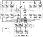
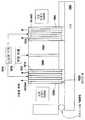
도 4 는 일 실시형태 하에서, 본 명세서에서 다중 채널 사이트-분리된 반응기 (MCSIR: Multiple Channel Site-Isolated Reactor) 라고 불리는 통합된 처리 도구의 블록도이다.4 is a block diagram of an integrated processing tool, referred to herein as a Multiple Channel Site-Isolated Reactor (MCSIR), under one embodiment.
도 5 는 일 실시형태 하에서, MCSIR 의 사이트-분리된 처리 모듈 (SIPM: site-isolated processing module) 이다.5 is a site-isolated processing module (SIPM) of MCSIR, under one embodiment.
도 6 은 일 실시형태 하에서, SIPM 의 구성 성분들의 서브세트 간의 커플링을 나타낸다.6 illustrates coupling between a subset of the components of a SIPM, under one embodiment.
도 7 은 일 실시형태 하에서, 독립 프로세스 경로 및 폐기물 경로를 포함한 흐름 셀의 블록도이다.7 is a block diagram of a flow cell including an independent process path and a waste path, under one embodiment.
도 8 은 기판의 혼합-모드 처리의 플로 다이어그램이다.
도 9 는 일 실시형태 하에서, 척에 메이팅된 흐름 셀 어셈블리를 포함하는 MCSIR 을 나타낸다.8 is a flow diagram of mixed-mode processing of a substrate.
9 illustrates an MCSIR comprising a flow cell assembly mated to a chuck, under one embodiment.
도 10 은 일 실시형태 하에서, 유체 역학적 시일링 (hydrodynamic sealing) 시스템을 나타낸다.FIG. 10 shows a hydrodynamic sealing system, under one embodiment.
상세한 설명details
본 명세서에서 다중 채널 사이트-분리된 반응기 (MCSIR: Multiple Channel Site-Isolated Reactor) 라고 불리는 통합된 처리 도구가 이하에서 서술된다. MCSIR 은 풀-웨이퍼 처리 모듈 및 조합형, 사이트-분리된 처리 모듈로 구성된다. 통합 처리 도구의 주 목적은 풀-기판과 그 풀-기판의 다수의, 사이트-분리된 영역들 간에 혼합-모드 처리를 실행하는 것이다. 이렇게, 처리 모듈들에서 사용하는 화학 약품들은 그 조성이 조합 방식으로 변화될 수 있고 그 구성물들이 프로세스 시퀀스에 대한 레시피의 일부로서 구체화될 수 있는 용액의 생성을 가능하게 하는 제 1 매니폴드들의 세트를 포함하는 공통 전달 시스템으로부터 공급된다. 용액의 완전한 혼합뿐만 아니라 정확한 온도 및 pH 제어를 허용하기 위하여, 각 제 1 매니폴드의 출력은 적어도 하나의 혼합 용기에 결합된다. 각각의 혼합 용기의 출력은 실질적으로 제 2 매니폴드들의 하나 이상의 세트로 배분된다. 제 2 매니폴드의 각 세트의 출력은 처리 모듈의 하나 이상의 반응기들에 공급한다. 혼합 용기에서 정적으로 혼합되는 용액을 제공하는 것에 더하여, 매니폴드들의 제 2 세트는 다수의 화학 약품들이 동시에 분배되어 용액의 동적, 인-라인 혼합을 용이하게 한다.An integrated processing tool referred to herein as a Multiple Channel Site-Isolated Reactor (MCSIR) is described below. MCSIR consists of a full-wafer processing module and a combination, site-separated processing module. The main purpose of the integrated processing tool is to perform mixed-mode processing between the full substrate and the multiple, site-separated regions of the full substrate. As such, the chemicals used in the processing modules may include a set of first manifolds that allow the creation of a solution whose composition can be varied in a combinatorial fashion and whose components can be embodied as part of a recipe for a process sequence. It is supplied from a common delivery system that includes. In order to allow full mixing of the solution as well as accurate temperature and pH control, the output of each first manifold is coupled to at least one mixing vessel. The output of each mixing vessel is distributed substantially to one or more sets of second manifolds. The output of each set of second manifolds feeds one or more reactors of the processing module. In addition to providing a solution that is statically mixed in the mixing vessel, a second set of manifolds allows multiple chemicals to be dispensed simultaneously to facilitate dynamic, in-line mixing of the solution.
사이트-분리된 처리에 대해서, MCSIR 은 풀 기판 상의 다수의 독립 사이트를 집합적으로 어드레싱하는 다수의 독립적으로 제어된 프로세스 챔버를 통합한다. MCSIR 은 직렬 방식 및/또는 병렬 방식의 하나 이상의 방식으로 다양한 화학 약품 용액 또는 조성물을 혼합하고 기판 상에 분배하는 능력을 제공하고, 임의의 수의 반응기들이나 반응기들의 하나 이상의 서브셋에 대해 흐름 및/또는 용액의 조성을 독립적으로 변화시키는 능력을 제공한다. MCSIR 은 프로세스 시퀀스에 대한 광역적 파라미터가 사이트-분리되지 않은 제어 파라미터 (웨이퍼 기판의 온도, 반응기 높이/체적 등) 들에 대한 이러한 유형의 동기화를 요구하는 경우 프로세스 단계들을 동기화하고 모든 사이트-분리된 반응기들에 걸쳐 임계 타이밍을 제어하는 능력을 제공한다.For site-separated processing, the MCSIR incorporates a number of independently controlled process chambers that collectively address a number of independent sites on a full substrate. MCSIR provides the ability to mix and dispense various chemical solutions or compositions on a substrate in one or more ways in a tandem and / or parallel manner, and to flow and / or to any number of reactors or one or more subsets of reactors It provides the ability to change the composition of the solution independently. MCSIR synchronizes process steps and all site-separated if global parameters for the process sequence require this type of synchronization for non-site-separated control parameters (wafer substrate temperature, reactor height / volume, etc.). It provides the ability to control critical timing across the reactors.
단일 200-㎜ 또는 300-㎜ 실리콘 기판에 걸쳐 다수의 독립적으로-제어되고 부설된 반응기 또는 프로세스 챔버들을 제공함으로써, 본 명세서에 있어서 서술된MCSIR 은 종래의 반도체 제조 장비로 하여금 재료 조사 및 통합에 적합하지 않게 하는 문제들을 해결한다. 각 사이트-분리된 반응기의 구성 및 흐름 역학은 통상 제조 반응기로부터 스케일링되어 프로세스 통합 시퀀스에 대한 최소 변화로 풀 웨이퍼에 대한 프로세스 스케일-업을 용이하게 한다. 또한, MCSIR 의 재료 전달 시스템은 챔버에 제공되는 재료의 수뿐만 아니라 재료 통합을 달성하는데 이용되는 프로세스 시퀀스의 단계들 양자 모두에서 보다 큰 유연성을 갖도록 구성된다. 재료 연구 및 통합을 위한 반응기의 소형화 및 완화된 장비 요건은 또한 제조 도구에 비해 장비의 비용을 절감시킨다.By providing a number of independently-controlled and laid reactors or process chambers over a single 200-mm or 300-mm silicon substrate, the MCSIR described herein makes conventional semiconductor manufacturing equipment suitable for material investigation and integration. Solve problems that prevent you from doing so. The configuration and flow kinetics of each site-separated reactor is typically scaled from the manufacturing reactor to facilitate process scale-up for the full wafer with minimal changes to the process integration sequence. In addition, MCSIR's material delivery system is configured to have greater flexibility in both the number of materials provided to the chamber as well as the steps of the process sequence used to achieve material integration. Reactor miniaturization and relaxed equipment requirements for material research and integration also reduce the cost of equipment compared to manufacturing tools.
기판을 처리하기 위한 시스템 및 방법 (예를 들어, 기판 상에 재료를 형성하기 위한 시스템 및 방법) 은 이하에서 기술된다. 본 명세서에서 "기판 처리 시스템 (SPS: substrate processing system)" 이라고 집합적으로 불리는 기판을 처리 하는 시스템 및 방법은 이하에서 상세히 기술되는 바와 같이 조합형 처리, 종래의 기판 처리와 통합된 조합형 프로세스 시퀀스, 및/또는 사이트-분리된 처리를 포함한다. 일 실시형태의 SPS 는 매우 적은 비용에서 기판 상의 매우 작은 (예를 들어, 나노 크기 규모에서) 구조물 또는 피쳐의 제조를 가능하게 하며, 이것은 예를 들어, 전자 컴포넌트 및 평판 패널 디스플레이와 같은 다양한 제품의 상용 제조에 유용할 수 있다. 이하에서 기술되는 다양한 시스템 및 방법은 예시로서만 나타내고 조합형 처리, 종래의 기판 처리와 통합된 조합형 프로세스 시퀀스 및/또는 사이트-분리된 처리의 특정 조합으로 본 명세서에서 서술되고 청구된 시스템 및 방법을 제한하도록 의도되지 않는다. 더욱이, 이하에서 서술되는 시스템 및 방법은 특정 프로세스 (예를 들어, 습식 프로세스, 건식 프로세스 등) 에 제한되지 않는다.Systems and methods for treating a substrate (eg, systems and methods for forming a material on a substrate) are described below. Systems and methods for processing substrates collectively referred to herein as " substrate processing system (SPS) " include combination processing, combination process sequences integrated with conventional substrate processing, and described in detail below; And / or site-separated treatment. The SPS of one embodiment enables the fabrication of very small (eg, on a nano-scale) structure or feature on a substrate at a very low cost, which can be used for various products such as, for example, electronic components and flat panel displays. It may be useful for commercial manufacture. The various systems and methods described below are by way of example only and limit the systems and methods described and claimed herein to specific combinations of combined processing, combined process sequences integrated with conventional substrate processing, and / or site-separated processing. It is not intended to be. Moreover, the systems and methods described below are not limited to specific processes (eg, wet processes, dry processes, etc.).
다음의 설명에서, 다양한 구체적 상세함은 SPS 의 실시형태에 대한 완전한 이해와 그에 대한 가능한 설명을 제공하도록 도입된다. 그러나, 관련 기술에서의 당업자는 하나 이상의 구체적 상세함 없이 또는 다른 컴포넌트, 시스템 등을 가지고 실시될 수 있다. 다른 경우, 공지된 구조물 또는 동작은 개시된 실시형태의 양태를 모호하게 하는 것을 방지하기 위하여 도시되지 않고, 또한 상세히 기술되지 않는다.In the following description, numerous specific details are introduced to provide a thorough understanding of the embodiments of the SPS and a possible description thereof. However, one of ordinary skill in the art may practice without one or more specific details or with other components, systems, or the like. In other instances, well-known structures or operations are not shown in order to avoid obscuring aspects of the disclosed embodiments and are not described in detail.
일 실시형태의 SPS 는 일반적으로 적어도 하나의 기판을 수용하도록 구성된 적어도 하나의 인터페이스를 포함한다. SPS 는 또한 인터페이스에 결합된 다수의 모듈을 포함한다. 본 명세서에서 컴포넌트로서 불리는 모듈은 또한 사전-처 리 모듈, 처리 모듈, 및 사후-처리 모듈을 포함하나, 다른 모듈에 대한 임의의 수 및/또는 유형을 포함할 수도 있으며, 여기서 모듈들 중 어느 하나가 사전-처리 모듈, 처리 모듈, 및/또는 사후-처리 모듈의 기능들을 포함할 수 있다. SPS 는 어느 특정 모듈 유형의 각각에 대해 적어도 하나를 포함하도록 요구되지 않는다. 또한, 사전-처리 모듈, 처리 모듈 및 사후-처리 모듈의 모두에 대한 기능들은 단일 모듈 내에 내장될 수도 있다. 다수의 모듈들 중 각 모듈은 모듈들 중 적어도 하나의 다른 모듈에 포함된 프로세스들에 적당한 다수의 상이한 프로세스들 중 적어도 하나를 포함할 수 있다. SPS 는 또한 인터페이스에 결합되고 인터페이스와 하나 이상의 모듈들 간에서 기판을 이동시키도록 구성된 적어도 하나의 핸들러를 포함한다.An SPS of one embodiment generally includes at least one interface configured to receive at least one substrate. The SPS also includes a number of modules coupled to the interface. Modules, referred to herein as components, also include pre-processing modules, processing modules, and post-processing modules, but may include any number and / or type for other modules, wherein any one of the modules May include the functions of a pre-processing module, a processing module, and / or a post-processing module. The SPS is not required to include at least one for each of any particular module type. In addition, the functions for all of the pre-processing module, the processing module and the post-processing module may be embedded in a single module. Each module of the plurality of modules may include at least one of a number of different processes suitable for processes included in at least one other module of the modules. The SPS also includes at least one handler coupled to the interface and configured to move the substrate between the interface and one or more modules.
도 1 은 일 실시형태에 따른, 기판 처리 시스템 (SPS) (100) 이다. 기판 처리 시스템 (100) 은 사전-처리 모듈 (101), 처리 모듈 (102) 및 사후-처리 모듈 (103) 을 포함한다. SPS (100) 는 각각의 상기 모듈 유형에 대해 적어도 하나를 포함하도록 요구되지 않는다; 예를 들어, 특정 프로세스 흐름은 오직 처리 모듈 (102) 과, 기판을 시스템 (100) 안으로 및 밖으로 이동시키는 수단만을 포함할 수도 있다. 또한, 사전-처리 모듈, 처리 모듈 및 사후-처리 모듈 모두의 기능은 단일 모듈 내부에 내장될 수도 있다. 모듈들 (101, 102, 및 103) 은 모듈들 (101, 102, 및 103) 이 사용될 것인 기판 처리의 유형에 적절한 장치 (특히, 종래의 상용 기판 처리 장치) 를 이용하여 각각 구현될 수 있다. 모듈 (101, 102, 및 103) 은 기판 및/또는 프로세스의 특성에 따라 변경 및/또는 추가로 구현될 수 있다.1 is a substrate processing system (SPS) 100, according to one embodiment. The
기판은 또한 공장 인터페이스 (104) 로서 불리는 시스템 인터페이스 (104) 를 통해 시스템 (100) 에 출입한다. 단일 기판이 시스템 (100) 내에서 한번에 처리될 수 있거나 다수의 기판들이 배치식으로 동시에 처리될 수 있다. 시스템 인터페이스 (104) 는 기판(들)을 시스템 (100) 안으로 및 밖으로 이동시키는 기판 핸들러 (104a) (이것은 예를 들어, 로봇을 이용하여 구현될 수 있다) 를 포함한다. 기판을 시스템 (100) 안으로 및 밖으로 이동시키는 것을 용이하게 하기 위하여, 시스템 인터페이스 (104) 는 기판 로드 스테이션 (104b) 및 기판 언로딩 스테이션 (104c) (또한, 각각 전면 개방 통합된 포드 (FOUP: Front Opening Unified Pod) 로드 스테이션 (104b) 및 FOUP 언로드 스테이션 (104c) 로 불림) 을 포함한다.The substrate enters and exits the
처리된 기판(들)이 시스템 (100) 으로부터 제거되고, 기판 핸들러 (104a) 에 의해 (또다른 위치로의 최종적 이동을 위해) 기판 언로드 스테이션 (104c) 에 놓인 후, 기판 로드 스테이션 (104b) 상에 이미 놓여진 새로운 기판(들)은 기판 핸들러 (104a) 에 의해 기판 로드 스테이션 (104b) 으로부터 취해지고, 처리를 위해 시스템 (100) 으로 이동된다. (기판 핸들러 (104a), 기판 로드 스테이션 (104b) 및 기판 언로드 스테이션 (104c) 을 포함한) 시스템 인터페이스 (104) 는 기판을 처리하는 분야의 당업자에게 공지된 종래의 장치 및 방법들을 이용하여 구현될 수 있다. 하나 이상의 다른 실시형태들의 시스템 (100) 은 다수의 시스템 인터페이스들을 포함할 수 있으며, 각각은 상술한 바와 같이 구성되고 동작될 수 있다.The processed substrate (s) is removed from the
일단 시스템 (100) 에서, 기판 취급 시스템 (105) 은 시스템 (100) 의 상이한 모듈들 (101-103) 사이에서 시스템 (100) 에 의해 처리되는 기판(들)을 이동하도록 사용될 수 있다. 시스템 인터페이스 (104) 의 기판 핸들러 (104a) 와 같이, 기판 취급 시스템 (105) 은 예를 들어, 하나 이상의 로봇들을 이용하여 구현될 수 있다. 모듈들 (101, 102, 및 103) 이 습식 처리 모듈 및 건식 처리 모듈 양자 모두를 포함하면, 기판 취급 시스템 (105) 은 적어도 2 종류의 장치를 포함한다: 건식 처리 모듈 및 시스템 인터페이스 (104) 안으로 및 밖으로 그리고 건조 모듈 밖으로 기판(들)을 이동시키는 건식 기판 핸들러와, 습식 처리 모듈 안으로 및 밖으로 그리고 건조 모듈 안으로 기판(들)을 이동시키는 습식 기판 핸들러. 기판 취급 시스템 (105) 은 기판을 처리하는 분야의 당업자에게 공지된 장치 및 방법들을 이용하여 구현될 수 있다.Once in
기판(들)이 시스템 인터페이스 (104) 를 통해 시스템 (100) 안으로 또는 밖으로 이동 중에 있는 경우 이외에는, 시스템 (100) 이 외부 환경으로부터 시일링된다. 시스템 (100) 에 의해 실시될 처리에 따라서, 사전-처리 모듈 (101), 처리 모듈 (102) 및 사후-처리 모듈 (103) 의 외부에 있는 시스템 (100) 내의 환경 (편의상, 이하에서 종종 "시스템 환경" 이라 불림) 은 대기압 하에 유지되고, 진공 하에 유지되며, 및/또는 가압 (즉, 대기압 위의 압력 하에서 유지) 될 수 있다. 유사하게, 시스템 환경은 시스템 (100) 밖의 환경에 대한 주위 온도에서 또는 그 주위 온도보다 높거나 낮은 온도에서 유지될 수 있다.The
게다가, 시스템 환경의 가스 조성은 원하는 바와 같이 제어될 수 있다. 예를 들어, 시스템 환경은 (통상, 외부 환경으로부터의 오염을 저감하도록 제어된) 대기일 수 있다. 시스템 환경은 또한 전체 또는 일부에서 특정 가스 또는 가스들을 포함하도록 제어될 수 있으며, 예를 들어, 반도체 웨이퍼들을 처리하도록 사용된 시스템에서는, 시스템 환경이 질소 가스 또는 불활성 가스 상태이도록 제어될 수 있다. 시스템 환경은 또한 특정 가스 또는 가스들을 배제하도록 제어될 수 있으며, 예를 들어, 시스템 환경으로부터 산소가 배제되어 시스템 내에 처리된 기판(들) (또는 그 기판 상에 형성된 재료(들)) 의 산화의 발생을 저감할 수 있다.In addition, the gas composition of the system environment can be controlled as desired. For example, the system environment may be atmosphere (typically controlled to reduce contamination from the external environment). The system environment may also be controlled to include certain gases or gases in whole or in part, for example, in a system used to process semiconductor wafers, the system environment may be controlled to be in a nitrogen gas or inert gas state. The system environment may also be controlled to exclude certain gases or gases, for example, by excluding oxygen from the system environment, thereby allowing oxidation of the substrate (s) (or material (s) formed on the substrate) processed in the system. The occurrence can be reduced.
다른 실시형태의 SPS 는 단일 웨이퍼 또는 웨이퍼들의 단일 배치를 처리하는데 사용되는 다수의 각 유형의 모듈을 포함할 수 있고; 그러므로, 다수의 버전의 SPS 는 단일 시스템으로 병렬로 동작될 수 있다. 이것은 SPS 에 의해 처리된 기판의 쓰루풋을 개선할 수 있다. 이것은 또한 리던던시를 추가하여 시스템 이용가능성이 심지어 시스템의 하나 이상의 모듈이 소정 기간의 시간 동안 (예를 들어, 예방적 유지 관리, 수선 등 동안) 비-동작적으로 되게 하는 경우에도 유지될 수 있다.Other embodiments of the SPS may include a number of each type of module used to process a single wafer or a single batch of wafers; Therefore, multiple versions of SPS can be operated in parallel in a single system. This can improve the throughput of the substrate processed by the SPS. This can also be maintained if the addition of redundancy causes system availability to become non-operational even for one or more modules of the system (eg, during preventive maintenance, repair, etc.) for a period of time.
상술한 SPS 는 일례로서 나타내고, 다른 수의 처리 모듈을 포함한 시스템이 사용될 수 있다. 또한, 상술한 이들과 다른 처리 모듈의 유형들이 사용될 수 있다. 기판(들) 의 수동 로딩 및 언로딩이 시스템 안으로 및 밖으로 기판(들)을 이동시키기 위해 기판 핸들러 대신 일부 처리 시스템에서 사용될 수도 있다.The above-described SPS is shown as an example, and a system including other numbers of processing modules may be used. Also, these and other types of processing modules may be used. Manual loading and unloading of the substrate (s) may be used in some processing systems instead of the substrate handler to move the substrate (s) into and out of the system.
상술한 SPS (100) 는 단일 기판 상의 영역들을 조합적으로 처리하기 위해 하나 이상의 모듈들 (또한 컴포넌트들이라고 불림) 및/또는 방법들을 포함할 수 있 다. 일반적으로, 영역들의 어레이는 기판 상의 하나 이상의 영역들에 처리 재료들을 전달하는 것 및/또는 그 영역들을 변경하는 것에 의해 조합적으로 처리된다. 일 실시형태의 기판 상의 영역들은 미리-정의된 영역들 및/또는 기판의 처리 동안 및/또는 기판의 처리 결과로서 식별된 영역들을 포함하나 이에 제한되지 않는다.The above-described
도 2 는 일 실시형태 하에서, 조합형 프로세스 시퀀스의 통합에 대한 흐름도이다. 실시형태는 분석을 위해 원하는 프로세스를 실시할 (효과적인 단위 프로세스를 총체적으로 실시하는 이산적인 단위 모듈들로 구성된 통합된 도구일 수도 있거나 아닐 수도 있는) 처리 도구를 이용할 수도 있다. 일 실시형태에서, 처리 도구는 IC 제조 시 사용된 300㎜ 직경 웨이퍼와 같이 단일 모놀리스 (monolithic) 기판에 포함된 고유한 영역들 내에서 이산화된 방식으로 프로세스를 실시할 수 있다. 기판은 시스템에 제공되고 (200), 이산화된, 바람직하게는 분리된 방식 (직렬 모드, 병렬 모드, 또는 직렬-병렬 모드 중 어느 하나) 으로 처리되어 기판의 적어도 2 개 영역들이 서로 상이하게 처리된다 (210). 조합 방식으로 처리되는 기판은 선택적으로 적어도 하나의 프로세스 또는 프로세스 단계와 함께 종래의 방식으로 이전에 (220) 및/또는 후속하여 (230) 처리될 수 있으므로, 전체 기판 또는 실질적으로 전체 기판에 가까운 기판이 동일한 처리 조건에 종속된다. 이것은 서술된 조합형 처리/조합형 프로세스 시퀀스 통합의 접근법으로 하여금 최종 디바이스(들), 집적 회로 등을 만드는데 요구된 프로세스 흐름의 원하는 세그먼트들 내에서 사용되게 한다.2 is a flow diagram for the integration of a combined process sequence, under one embodiment. An embodiment may use a processing tool (which may or may not be an integrated tool consisting of discrete unit modules that collectively perform an effective unit process) to perform the desired process for analysis. In one embodiment, the processing tool may perform the process in a discretized manner within the unique areas contained in a single monolithic substrate, such as a 300 mm diameter wafer used in IC fabrication. The substrate is provided to the system (200) and processed in a discrete, preferably discrete manner (either serial mode, parallel mode, or series-parallel mode) so that at least two regions of the substrate are treated differently from one another. (210). Substrates that are treated in a combination manner can optionally be treated (220) and / or subsequently (230) previously in a conventional manner with at least one process or process step, so that the substrate is substantially or substantially close to the entire substrate. This depends on the same processing conditions. This allows the described combined processing / combined process sequence integration approach to be used within the desired segments of the process flow required to make the final device (s), integrated circuits, and the like.
디바이스들 또는 생성된 디바이스들의 일부와 같이 처리된 영역들은 저항, 선 저항, 정전용량 등을 통해 수율과 같은 특성에 대한 파라미터 검사 및/또는 스트레스 이동, 전자 이동 (electromigration), 바이어스 열 스트레스, 시간 의존 유전체 파괴와 같은 특성에 대한 신뢰성 검사와 당업자에게 공지된 관련 검사와 같이, 분석을 위한 종래의 방법들을 이용하여 관심 있는 특성에 대해 검사될 수 있다. 처리된 영역들은 동시에, 순차적으로, 또는 제 1 복수의 영역들이 동시에 검사되고, 이어서 제 2 복수의 영역들이 동시에 검사되는 병렬-직렬 모드로 검사될 수 있다. 검사 (240) 는 부가적으로 조합형 프로세스 시퀀스 통합을 위한 방법론의 하나 이상의 다른 실시형태로 실시된다.Processed areas, such as devices or some of the devices produced, can be parametrically inspected for properties such as yield and / or stress transfer, electromigration, bias thermal stress, time dependence through resistance, line resistance, capacitance, etc. The properties of interest can be examined using conventional methods for analysis, such as reliability tests for properties such as dielectric breakdown and related tests known to those skilled in the art. The processed regions can be examined simultaneously, sequentially, or in a parallel-serial mode in which the first plurality of regions are examined at the same time and then the second plurality of regions are examined at the same time.
일 실시형태의 조합형 프로세스 시퀀스 통합은 하나 이상의 프로세스들을 실시하는 본 명세서에서 사이트-분리된 처리 도구 (또한 사이트-분리된 반응기 (SIR: site-isolated reactor) 로서 불림) 로서 불리는 처리 도구를 사용한다. 일 실시형태에서, 사이트-분리된 처리 도구는 기판의 고유한 영역들 내에서 이산화되고, 분리된 방식 (직렬 모드, 병렬 모드, 또는 직렬-병렬 모드 중 어느 하나) 으로 기판을 처리한다 (예를 들어, 기판의 적어도 2 개 영역들이 서로 상이하게 처리된다). 어레이의 영역들의 처리 시, 본 명세서에서 상술한 바와 같이, 처리하는 재료들은 (미리 정의된 영역들을 포함한) 기판상의 영역들로 전달될 수 있고/있거나 (미리 정의된 영역들을 포함한) 영역들은 임의의 수의 종래의 처리 프로세스 또는 시퀀스와 함께 임의의 수의 사이트-분리된 처리 프로세스 또는 시퀀스를 이용하여 변경될 수 있다.The combined process sequence integration of one embodiment uses a processing tool, referred to herein as a site-isolated reactor (SIR), which performs one or more processes. In one embodiment, the site-separated processing tool is discretized within the intrinsic regions of the substrate and processes the substrate (either in serial mode, parallel mode, or series-parallel mode) in a separate manner (eg, For example, at least two regions of the substrate are treated differently from each other). In the processing of regions of the array, as described herein above, the materials to be treated can be transferred to regions on the substrate (including predefined regions) and / or the regions (including predefined regions) It can be changed using any number of site-separated processing processes or sequences with any number of conventional processing processes or sequences.
예를 들어, 본 명세서에서 서술된 조합형 프로세스 시퀀스 통합 하에서의 방법은 성막, 패터닝, 에칭, 세정, 평탄화, 주입 및 검사를 포함한 그룹으로부터 선택된 적어도 하나의 제 1 프로세스로부터 기판을 수용한다. 그 방법은 기판의 적어도 하나의 영역을 기판의 적어도 하나의 다른 영역과 상이하게 처리하여 처리된 기판을 생성한다. 처리는 적어도 하나의 영역을 변경하는 것 (modifying) 을 포함하며, 여기서 변경은 물리적 변경, 화학적 변경, 전기적 변경, 열적 변경, 자기적 변경, 광자적 변경 및 광분해적 변경 중 적어도 하나를 포함한다. 처리는 기판 상에 상이하게 처리된 영역들의 적어도 하나의 어레이를 형성한다. 일 실시형태에서, 상술한 처리는 재료, 처리 조건, 프로세스 시퀀스, 프로세스 시퀀스 통합, 및 프로세스 시퀀스 조건 중 적어도 하나를 이용한 변경을 포함한다. 하나의 다른 실시형태에서, 상술한 처리된 기판은 성막, 패터닝, 에칭, 세정, 평탄화, 주입 및 검사를 포함한 그룹으로부터 선택된 적어도 하나의 추가적 프로세스를 받는다.For example, the method under the combined process sequence integration described herein receives a substrate from at least one first process selected from the group including deposition, patterning, etching, cleaning, planarization, implantation and inspection. The method treats at least one region of the substrate differently from at least one other region of the substrate to produce a processed substrate. The treatment includes modifying at least one region, where the alteration includes at least one of a physical alteration, a chemical alteration, an electrical alteration, a thermal alteration, a magnetic alteration, a photon alteration and a photolytic alteration. The processing forms at least one array of differently processed regions on the substrate. In one embodiment, the processing described above includes a change using at least one of material, processing conditions, process sequence, process sequence integration, and process sequence conditions. In one other embodiment, the treated substrate described above is subjected to at least one additional process selected from the group including deposition, patterning, etching, cleaning, planarization, implantation and inspection.
또다른 예로서, 본 명세서에서 서술된 조합형 프로세스 시퀀스 통합은 기판의 적어도 하나의 영역을 기판의 적어도 하나의 다른 영역과 상이하게 처리함으로써 처리된 기판을 생성한다. 처리는 적어도 하나의 영역을 변경하는 것을 포함하며, 여기서 변경은 물리적 변경, 화학적 변경, 전기적 변경, 열적 변경, 자기적 변경, 광학적 변경, 및 광분해적 변경 중 적어도 하나를 포함한다. 처리는 기판 상에서 상이하게 처리된 영역들의 적어도 하나의 어레이를 형성한다. 그 방법은 성막, 패터닝, 에칭, 세정, 평탄화, 주입 및 검사를 포함한 그룹으로부터 선 택된 적어도 하나의 추가적 프로세스에 처리된 기판을 제공함으로써 계속된다. 일 실시형태에서, 상술한 처리는 재료, 처리 조건, 프로세스 시퀀스, 프로세스 시퀀스 통합 및 프로세스 시퀀스 조건 중 적어도 하나를 이용한 변경을 포함한다.As another example, the combined process sequence integration described herein produces a processed substrate by treating at least one region of the substrate differently from at least one other region of the substrate. Processing includes changing at least one region, where the change includes at least one of a physical change, a chemical change, an electrical change, a thermal change, a magnetic change, an optical change, and a photolytic change. The processing forms at least one array of differently processed regions on the substrate. The method continues by providing the treated substrate to at least one additional process selected from the group including deposition, patterning, etching, cleaning, planarization, implantation and inspection. In one embodiment, the above-described processing includes a change using at least one of material, processing condition, process sequence, process sequence integration, and process sequence condition.
도 3 은 일 실시형태 하에서, 사이트-분리된 처리 및/또는 종래의 처리를 포함하는 조합형 프로세스 시퀀스 통합의 프로세스 흐름 (300) 이다. 본 실시형태 하에서의 처리 시퀀스의 일례는 다음과 같다: 종래의 프로세스 N 을 이용하여 기판을 처리, 이후 사이트-분리된 프로세스 N+1 을 이용하여 기판을 처리, 다음으로 사이트-분리된 프로세스 N+2 를 이용하여 기판을 처리, 그 다음 종래의 프로세스 N+3 을 이용하여 기판을 처리, 그 후 E-검사 (예를 들어, 전기적 검사) 를 실시. 본 실시형태 하에서의 처리 시퀀스의 또다른 예는 다음과 같다: 사이트-분리된 프로세스 N 을 이용하여 기판을 처리, 이후 사이트-분리된 프로세스 N+1 을 이용하여 기판을 처리, 다음으로 종래의 프로세스 N+2 를 이용하여 기판을 처리, 그 다음 사이트-분리된 프로세스 N+3 을 이용하여 기판을 처리, 그 후 E-검사를 실시. 본 실시형태 하에서의 처리 시퀀스의 또다른 예는 다음과 같다: 사이트-분리된 프로세스 N 을 이용하여 기판을 처리, 이후 종래의 프로세스 N+1 를 이용하여 기판을 처리, 다음으로 사이트-분리된 프로세스 N+2 를 이용하여 기판을 처리, 그 다음 종래의 프로세스 N+3 을 이용하여 기판을 처리, 그 후 E-검사를 실시. 다양한 다른 처리 시퀀스는 프로세스 흐름 (300) 에 따라 달성될 수 있다.3 is a
이로써, 조합형 프로세스 시퀀스 통합은 예를 들어, 테스트 다이 및/또는 의도된 집적 회로를 포함한 실제 제품 다이일 수 있는 복수의 다이 (304) 를 구비하 는 다이 어레이를 포함한 반도체 웨이퍼 (302) 를 생성한다. 블랭킷 웨이퍼, 패턴 웨이퍼, 디바이스, 기능 칩, 기능 디바이스, 테스트 구조체, 반도체, 집적 회로, 평면 패널 디스플레이, 광전자 디바이스, 데이터 저장 디바이스, 자기 전자 디바이스, 자기 광학 디바이스, 분자 전자 디바이스, 태양 전지, 광 디바이스, 및 패키징된 디바이스는 상술한 조합형 프로세스 시퀀스 통합 방법론을 이용하여 처리 및/또는 생성될 수 있다. 조합형 프로세스 시퀀스 통합은 전체 프로세스 흐름의 임의의 원하는 세그먼트(들) 및/또는 일부(들)에 적용될 수 있다. 전기적 검사를 포함하는 특성 평가는 각 프로세스 단계 및/또는 필요 및/또는 희망에 따라 프로세스 흐름 내의 일련의 프로세스 단계들 후에 실시될 수 있다.As such, the combined process sequence integration produces a
SPS 의 실시형태는 기판상의 하나 이상의 미리 정의된 영역에 처리 재료들을 전달하고, 다수의 상이한 기술을 이용하여 그 전달된 재료들을 반응시킨다. 예를 들어, 처리 재료들은 예를 들어, 용액 기반 합성 기술, 광 화학적 기술, 중합 기술, 템플릿에 의한 합성 기술, 에피텍셜 성장 기술, 졸-겔 프로세스에 의한 수단, 열, 적외선 또는 마이크로파 가열에 의한 수단, 소성, 소결 또는 어닐링에 의한 수단, 열수 방법, 플럭스 방법, 솔벤트 기화를 통한 결정화 수단 등을 이용하여 반응될 수 있다. 관심 있는 처리 재료들을 반응시키는데 사용될 수 있는 다른 유용한 반응 기술은 당업자에게 매우 명백할 것이다.Embodiments of an SPS deliver processing materials to one or more predefined areas on a substrate and react the transferred materials using a number of different techniques. For example, the treatment materials can be, for example, solution based synthesis techniques, photochemical techniques, polymerization techniques, synthesis techniques by templates, epitaxial growth techniques, means by sol-gel processes, by heat, infrared or microwave heating. It can be reacted using a means, by means of sintering, sintering or annealing, a hydrothermal method, a flux method, a crystallization means through solvent vaporization and the like. Other useful reaction techniques that can be used to react the treatment materials of interest will be very apparent to those skilled in the art.
기판의 영역들이 서로에 대해 독립적으로 처리되기 때문에, 다른 영역들에서의 처리 조건은 독립적으로 제어될 수 있다. 이와 같이, 프로세스 재료 양, 반응 솔벤트, 처리 온도, 처리 시간, 처리 압력, 반응이 제지되는 레이트, 프로세스 재료들의 성막 순서, 프로세스 시퀀스 단계 등은 기판 상의 영역마다 변화될 수 있다. 이로써, 예를 들어, 재료를 조사할 때, 제 1 영역 및 제 2 영역에 전달되는 처리 재료가 동일하거나 상이할 수 있다. 제 1 영역에 전달되는 처리 재료가 제 2 영역에 전달되는 처리 재료와 동일한 경우, 이 처리 재료는 동일한 농도 또는 상이한 농도 중 어느 하나에서 기판 상의 제 1 영역 및 제 2 영역에 제공될 수 있다. 이것은 제 1 영역 및 제 2 영역 등에 전달되는 추가적인 처리 재료에 대해서도 사실이다. 제 1 영역 및 제 2 영역에 전달되는 처리 재료의 경우와 같이, 제 1 영역 및 제 2 영역에 전달되는 추가적인 처리 재료는 동일하거나 상이할 수 있으며, 만약 동일한 경우, 동일한 농도 또는 상이한 농도 중 어느 하나에서 기판 상의 제 1 영역 및 제 2 영역에 제공될 수 있다.Since regions of the substrate are treated independently of each other, the processing conditions in other regions can be controlled independently. As such, the amount of process material, reaction solvent, process temperature, process time, process pressure, rate at which the reaction is stopped, deposition order of process materials, process sequence step, and the like may vary from region to region on the substrate. Thus, for example, when irradiating the material, the treatment materials delivered to the first region and the second region may be the same or different. If the processing material delivered to the first region is the same as the processing material delivered to the second region, the processing material may be provided to the first and second regions on the substrate at either the same concentration or at different concentrations. This is also true for the additional processing material delivered to the first and second zones and the like. As in the case of treatment materials delivered to the first and second regions, the additional treatment materials delivered to the first and second regions may be the same or different, and if they are the same, either the same or different concentrations. In the first region and the second region on the substrate.
또한, 기판 상의 주어진 미리 정의된 영역 내에서, 처리 재료는 균일한 방식 또는 그레디언트 (gradient) 방식으로 전달될 수 있다. 동일한 농도에서 기판의 제 1 영역 및 제 2 영역에 동일한 처리 재료들이 전달되면, 영역이 처리되는 조건 (예를 들어, 반응 온도, 반응 시간 등) 은 영역마다 변화될 수 있다. 변화될 수 있는 파라미터들은 예를 들어, 재료량, 솔벤트, 프로세스 온도, 프로세스 시간, 프로세스가 수행되는 압력, 프로세스가 행해지는 분위기, 프로세스가 제지되는 레이트, 재료들이 성막되는 순서 등을 포함한다. 변화될 수 있는 다른 프로세스 파라미터들은 당업자에게 명백할 것이다.Further, within a given predefined area on the substrate, the processing material can be delivered in a uniform manner or in a gradient manner. If the same treatment materials are delivered to the first region and the second region of the substrate at the same concentration, the conditions under which the region is processed (eg reaction temperature, reaction time, etc.) may vary from region to region. Parameters that can be changed include, for example, amount of material, solvent, process temperature, process time, pressure at which the process is performed, atmosphere in which the process is performed, rate at which the process is stopped, order in which materials are deposited, and the like. Other process parameters that can be changed will be apparent to those skilled in the art.
또한, 일 실시형태는 IC 칩 상의 영역들의 상이한 부분들을 나타내기 위하여 유전체 재료 표면 및 전기적 도전 표면과 같은 상이한 표면들을 갖는 제 1 표면과 제 2 표면 양자 모두에 대응한 영역들에 사실상 동일한 농도에서 동일한 처리 재료를 실질적으로 전달하여 재료에 대한 적어도 2 개의 상이한 어레이들을 형성하고, 그 후, 기판 상의 프로세스 재료들에 제 1 세트의 프로세스 조건을 행하기 위해 제공된다. 이 방법을 이용하여, 다양한 기판 표면에 프로세스 파라미터 또는 재료에 대한 결과가 연구되고, 다음으로 최적화될 수 있다.In addition, one embodiment is substantially equal in concentration to regions corresponding to both the first and second surfaces having different surfaces, such as the dielectric material surface and the electrically conductive surface, to represent different portions of the regions on the IC chip. Substantially transfer the processing material to form at least two different arrays of material, and then provide for subjecting the process materials on the substrate to a first set of process conditions. Using this method, the results for process parameters or materials on various substrate surfaces can be studied and then optimized.
개별 영역들의 처리 시 이용된 처리 재료는 종종 인접한 영역들로 이동되는 것이 방지되어야 한다. 가장 단순하게, 이것은 다양한 처리 재료들이 영역들 간에 상호 확산되지 않도록 기판 상의 영역들 간에 충분한 공간을 남김으로써 확보될 수 있다. 또한, 이것은 처리 시 기판 상의 다양한 영역들 간에 적절한 배리어를 제공하여 확보될 수 있다. 일 접근법에서, 기계적 디바이스 또는 물리적 구조물은 기판 상의 다양한 영역을 정의한다. 예를 들어, 벽 또는 다른 물리적 배리어는 개별 영역들 내의 재료들이 인접한 영역들로 이동되는 것을 방지하는데 사용될 수 있다. 이 벽 또는 물리적 배리어는 합성이 완료된 후 제거될 수도 있다. 당업자는 때때로, 재료들의 어레이를 선별하기 전에 그 벽 또는 물리적 배리어를 제거하는 것이 바람직할 수도 있다는 것을 이해할 것이다.The treatment material used in the treatment of the individual areas must often be prevented from moving to adjacent areas. In the simplest case, this can be ensured by leaving enough space between the regions on the substrate such that the various processing materials do not diffuse between the regions. This can also be ensured by providing an appropriate barrier between the various areas on the substrate during processing. In one approach, a mechanical device or physical structure defines various regions on the substrate. For example, a wall or other physical barrier can be used to prevent the materials in individual regions from moving to adjacent regions. This wall or physical barrier may be removed after synthesis is complete. Those skilled in the art will understand that sometimes it may be desirable to remove the wall or physical barrier prior to screening the array of materials.
다른 실시형태에서, 처리는 물리적으로 기판과 접촉하는 배리어의 필요성 없이 달성될 수도 있다. 예를 들어, 레이저, 방사성 램프, UV 복사 소스, 다른 "점" 소스는 변경의 면적이 기판 상의 관심 있는 이산 영역보다 크기에 있어서 명목상 작고/작거나 동일할 때 사이트 어드레스 가능한 방식으로 영역들을 처리하는데 사용될 수 있다. 또다른 실시형태에서, 물리적 배리어는 원하는 영역(들) 및/ 또는 물리적 배리어가 물리적으로 기판과 접촉하지 않는 영역(들)의 일부(들)에 대한 처리를 본질적으로 선별 및/또는 제한하는데 사용될 수 있다. 예를 들어, 물리적 배리어는 어떤 영역(들) 및/또는 영역(들)의 일부(들)에 대한 처리를 본질적으로 막고/막거나 한정하는데 사용될 수 있다. 마스크나 셔터와 같은 스크린은 예를 들어, PVD (즉, 스퍼터링) 또는 증착 소스로부터와 같은 증기 플럭스를 막는데 사용될 수 있다. 불투명 마스크 대 투명 마스크는 기판 상의 특정된 영역 내의 처리를 달성하기 위하여 투명 영역을 통해 어떤 복사를 허용하는데 사용될 수 있다. 또다른 실시형태에서, 바람직하게 아르곤 (Ar) 과 같은 불활성 가스의 가스 흐름은 기체 시약을 선별하고/선별하거나 이러한 시약의 농도를 제한하여 어떤 영역들에서 이러한 시약의 효과를 효과적으로 선별하는데 사용될 수 있다. 본 방식에서, 기판 상의 특정 영역들은 기판을 통해 물리적 배리어에 대한 필요 없이 상이하게 처리될 수 있다. 본 접근법은 특히 원자층 증착과 같은 순차적 기상 진공 기반 표면 운동 프로세스와 그 다양한 형태 (예를 들어, 이온, 라디칼, 및 플라즈마 유도/강화) 로 다루기 쉽다.In other embodiments, the processing may be accomplished without the need for a barrier in physical contact with the substrate. For example, lasers, radioactive lamps, UV radiation sources, and other "point" sources can process areas in a site addressable manner when the area of change is nominally small and / or the same in size than the discrete areas of interest on the substrate. Can be used. In another embodiment, the physical barrier can be used to essentially screen and / or limit the treatment to the desired region (s) and / or some (s) of the region (s) where the physical barrier does not physically contact the substrate. have. For example, a physical barrier can be used to essentially prevent and / or limit the treatment of a certain region (s) and / or a portion (s) of the region (s). Screens such as masks or shutters can be used to block vapor flux, such as, for example, from PVD (ie sputtering) or deposition sources. Opaque masks versus transparent masks can be used to allow some radiation through the transparent areas to achieve processing within specified areas on the substrate. In another embodiment, preferably, a gas stream of inert gas, such as argon (Ar), can be used to effectively screen the effects of such reagents in certain areas by screening gas reagents and / or limiting the concentration of such reagents. . In this manner, certain regions on the substrate can be treated differently without the need for a physical barrier through the substrate. This approach is particularly easy to handle in sequential vapor phase vacuum based surface motion processes such as atomic layer deposition and its various forms (eg, ions, radicals, and plasma induction / enhancement).
일 실시형태의 SPS 는 전체 기판에 걸쳐 균일한 처리 및 개별적으로 기판 상의 하나 이상의 이산 영역들의 독립적 처리 양자 모두를 달성하도록 구성된 처리 도구를 포함한다. 도 2 및 도 3 을 참조하여 상술된 조합형 프로세스 시퀀스 통합의 프로세스 흐름 하에서의 동작을 포함하는, 본 명세서에 서술된 처리 도구는 도 1 을 참조하여 상술한 SPS (100) 와 같은 기판 처리 시스템의 컴포넌트 및/또는 상술한 SPS (100) 의 하나 이상의 모듈일 수 있다. 도 3 의 조합형 프로세스 시퀀스 통합의 프로세스 흐름 (300) 은 예를 들어, SPS (100) (도 1) 의 처리 모듈 (102) 에서 구체화될 수 있다. 유사하게, 조합형 프로세스 시퀀스 통합의 프로세스 흐름 (300) 은 또다른 예로서 SPS (100) 의 하나 이상의 처리 모듈들 (101, 102, 및 103) (도 1) 에 걸쳐 구체화될 수 있다.The SPS of one embodiment includes a processing tool configured to achieve both uniform processing across the entire substrate and independent processing of one or more discrete regions on the substrate individually. The processing tools described herein, including the operation under the process flow of the combined process sequence integration described above with reference to FIGS. 2 and 3, may include components of a substrate processing system, such as the
일 실시형태의 SPS 는 풀-웨이퍼 처리 및 조합형 처리 양자 모두를 지원하는 통합된 처리 도구를 포함한다. 도 4 는 일 실시형태 하에서, 본 명세서에서 다중 채널 사이트-분리된 반응기 (MCSIR: Multiple Channel Site-Isolated Reactor) (400) 로서 불리는 통합된 처리 도구 (400) 의 블록도이다. MCSIR (400) 은 이하에서 상세히 서술되는 바와 같이 풀-웨이퍼 처리 모듈 (405), 사이트-분리된 처리 모듈 (SIPM: site-isolated processing module) (409) 을 포함한다. MCSIR (400) 은 프로세스 시퀀스를 실행하는데 필요한 생 (raw) 화학 약품들 (401) 을 제공하는 벌크 화학 약품 분배 시스템뿐만 아니라 혼합 용기 및 분배 매니폴드의 형태의 화학 약품 혼합 및 시퀀싱 하드웨어를 통합하여 임의의 조성의 화학 약품 용액들을 동적으로 혼합하는 것뿐만 아니라 임의의 시간 기간 동안 임의의 순서로 반응기들을 통해 화학 약품들을 시퀀싱하는 능력을 제공한다. MCSIR (400) 은 컴퓨터화된 하드웨어 제어기 (402) 를 이용하여 제어되고, 일 실시형태의 동일한 제어기는 풀-웨이퍼 반응기 및 사이트-분리된 반응기 양자 모두에서 처리를 달성한다. 웨이퍼들은 공장 인터페이스 (404) 를 이용하여 MCSIR (400) 을 통해 시퀀싱된다. 풀-웨이퍼 반응기 및 사이트-분리된 반응기는 모든 제어 양태들에서 유사하다. MCSIR (400) 의 각 반응기 또는 채널은 본 명세서에서 서술된 바와 같이 복잡한 습식/증기 프로세스 시퀀스들의 실시를 허용하도록 구성된다.The SPS of one embodiment includes an integrated processing tool that supports both full-wafer processing and combined processing. 4 is a block diagram of an
일반적으로, 풀-웨이퍼 처리 모듈 (405) 은 풀-웨이퍼 반응기에 결합된 프로세스 매니폴드를 포함한다. 프로세스 매니폴드는 화학 약품 (401) 에 연결되고 화학 약품 (401) 들을 풀-웨이퍼 반응기로 공급 또는 전달하도록 구성된다. 풀-웨이퍼 반응기는 전달된 화학 약품들을 이용하여 전체 웨이퍼 또는 기판 표면 (예를 들어, 8-인치 웨이퍼, 12-인치 웨이퍼, 등) 에 걸쳐 균일한 처리를 달성하도록 구성된다.In general, the full-
반면에, SIPM (409) 은 다수의 채널들 또는 프로세스 경로들을 이용하여 웨이퍼에 걸친 다수의 이산 영역들 (예를 들어, 28 개의 영역들) 의 독립적 처리를 가능케 하는 사이트-분리된 프로세서이다. SIPM (409) 의 본 실시예는 본 예의 명확함을 위해 2 개의 프로세스 경로들 또는 채널들 중 어느 하나에 의해 공급 중인 단일 사이트-분리된 반응기를 나타내나, MCSIR 은 임의의 수의 사이트-분리된 반응기 및 각 반응기에 접속된 임의의 수의 프로세스 경로들을 포함할 수 있다.In contrast,
SIPM (409) 은 제 1 매니폴드 (예를 들어, 혼합 용기 (MV: mixing vessel) 1 매니폴드) 들의 세트 또는 어셈블리를 일반적으로 포함한 전달 시스템을 이용하여 화학 약품 (401) 을 공급하거나 분배한다. 각 제 1 매니폴드의 출력은 혼합 용기 (예를 들어, 혼합 용기 1 등) 에 결합된다. 혼합 용기 매니폴드들은 혼합 용기들의 각각에 대해 임의의 비율로 벌크형 화학 약품들의 혼합을 허용하고, 이후 혼합 용기들은 혼합된 화학 약품 용액들에 대한 임시 저장소로서의 역할을 한다.
각 혼합 용기의 출력은 제 2 매니폴드들 (예를 들어, 프로세스 채널 1 사이 트 매니폴드, 프로세스 채널 2 사이트 매니폴드) 의 하나 이상의 세트에 공급한다. 제 2 매니폴드들의 각 세트의 출력은 사이트-분리된 반응기에 공급한다. 제 2 매니폴드들의 세트는 일반적으로 흐름 셀들의 세트에서 2 개의 프로세스 경로들 (예를 들어, 채널 1, 채널 2) 중 어느 하나를 통해 혼합 용기 용액들 및/또는 벌크형 화학 약품들의 시퀀싱을 허용한다. 흐름 셀들은 사이트-분리된 반응기의 상면을 포함하고, 반응기 슬리브 (sleeve) 들은 반응기의 측벽들을 포함한다. 처리된 기판은 반응기의 저부를 포함한다. 각 사이트-분리된 반응기는 본 명세서에서 서술되는 바와 같은 기판의 전용 영역의 개별 처리를 달성한다.The output of each mixing vessel feeds one or more sets of second manifolds (eg,
MCSIR (400) 의 실시예는 풀-웨이퍼 반응기에 대한 프로세스 경로 내에 혼합 용기를 포함하지 않는다. 그러나, SIPM 과 유사한 방식으로 풀-웨이퍼 처리 모듈을 구성하기 위하여 풀-웨이퍼 반응기 프로세스 경로 내에 혼합 용기를 포함하는 것이 가능하고 때론 바람직하다.Embodiments of
도 5 는 일 실시형태 하에서, MCSIR 의 SIPM (500) 이다. SIPM (500) 은 복수의 병렬 반응기에서 반응을 동시에 제어함으로써 기판의 상이한 영역들의 동시 처리를 관리하거나 제어한다. 각각의 반응기들은 기판 (예를 들어, 웨이퍼) 의 특정 영역에 근접하게 위치된다. 반응기 제어는 예를 들어, 시약 흐름, 시약 혼합, 시약 전달, 시약 온도 및/또는 반응기 온도, 및/또는 시약 pH 를 제어하는 것을 포함한다.5 is a
SIPM (500) 은 제 1 혼합 어셈블리 (514) 에 결합된 제 1 분배 어셈블리 (512) 를 포함한다. 제 1 분배 어셈블리 (512) 는 N 개의 혼합 용기 매니폴드 들 (5121 내지 512N) 을 포함하며, 여기서 혼합 용기 매니폴드들의 수 N 은 임의의 수일 수 있다. 일 실시형태의 제 1 분배 어셈블리 (512) 는 28 개의 혼합 용기 매니폴드들을 포함하나, SPS 는 이 수의 혼합 용기 매니폴드들에 제한되지 않고 임의의 수의 혼합 용기 매니폴드들을 포함할 수 있다. 혼합 용기 매니폴드들의 각각의 입력은 하나 이상의 화학 약품 (501) 에 결합된다. 일례로서, 일 실시형태의 혼합 용기 매니폴드는 8 개의 입력을 포함하며, 각각의 입력들은 상이한 하나의 화학 약품 (501) 에 접속된다. 혼합 용기 매니폴드는 그러나 8 개의 입력에 제한되지 않고, 각 입력은 임의의 다른 매니폴드 입력과 상이한 구성물에 대한 접속에 제한되지 않는다. 추가적으로, 분배 어셈블리 (512) 의 모든 혼합 용기 매니폴드들은 동일한 구성 상태에 제한되지 않는다. 또한, 다른 컴포넌트들 (예를 들어, 밸브, 조절기, 혼합기, 펌프 등) 은 구성물과 혼합 용기 매니폴드 간에 인라인으로 접속될 수 있다.
제 1 혼합 어셈블리 (514) 는 N 개의 혼합 용기들 (5141 내지 514N) 을 포함하며, 여기서 혼합 용기들의 수 N 은 임의의 수일 수 있다. 일 실시형태의 제 1 혼합 어셈블리 (514) 는 28 개의 혼합 용기들을 포함하나, SPS 는 이 수의 혼합 용기들에 제한되지 않고 임의의 수의 혼합 용기들을 포함할 수 있다. 혼합 용기들의 각각의 입력은 제 1 분배 어셈블리 (512) 의 혼합 용기 매니폴드의 출력에 결합된다. 일례로서, 일 실시형태의 혼합 용기는 제 1 분배 어셈블리 (512) 의 혼합 용기 매니폴드의 출력에 접속되는 1 개의 입력을 포함한다. 더 구체적인 예로서, 제 1 혼합 용기 (5141) 의 입력은 제 1 혼합 용기 매니폴드 (5121) 의 출 력에 접속된다. 혼합 용기는 그러나 1 개의 입력에 제한되지 않고, 각 입력은 제 1 분배 어셈블리 (512) 의 하나의 혼합 용기 매니폴드에 대한 접속에 제한되지 않는다.The
SIPM (500) 은 제 2 혼합 어셈블리 (524) 에 결합된 제 2 분배 어셈블리 (522) 를 더 포함한다. 제 2 분배 어셈블리 (522) 는 N 개의 혼합 용기 매니폴드들 (5221 내지 522N) 을 포함하며, 여기서 혼합 용기 매니폴드들의 수 N 은 임의의 수일 수 있다. 일 실시형태의 제 2 분배 어셈블리 (522) 는 28 개의 혼합 용기 매니폴드들을 포함하나, SPS 는 이 수의 혼합 용기 매니폴드들에 제한되지 않는다. 각각의 혼합 용기 매니폴드의 입력은 하나 이상의 화학 약품 (501) 에 결합된다. 일례로서, 그리고 상술한 바와 같이 일 실시형태의 혼합 용기 매니폴드는 8 개의 입력을 포함하며, 입력들의 각각은 하나의 상이한 화학 약품 (501) 에 접속된다. 혼합 용기 매니폴드는 그러나 8 개의 입력에 제한되지 않고, 각 입력은 임의의 다른 매니폴드의 입력과 상이한 구성물에 대한 접속에 제한되지 않는다. 추가적으로, 다른 컴포넌트들 (예를 들어, 밸브, 조절기, 혼합기, 펌프 등) 은 구성물과 혼합 용기 매니폴드 간에 인라인으로 접속될 수 있다.
제 2 혼합 어셈블리 (524) 는 N 개의 혼합 용기들 (5241 내지 524N) 을 포함하며, 여기서 혼합 용기들의 수 N 은 임의의 수일 수 있다. 일 실시형태의 제 2 혼합 어셈블리 (524) 는 28 개의 혼합 용기들을 포함하나, SPS 는 이 수의 혼합 용기들에 제한되지 않는다. 혼합 용기들의 각각의 입력은 제 2 분배 어셈블리 (522) 의 혼합 용기 매니폴드의 출력에 결합된다. 일례로서, 일 실시형태의 혼 합 용기는 제 2 분배 어셈블리 (522) 의 혼합 용기 매니폴드의 출력에 접속되는 1 개의 입력을 포함한다. 더 구체적인 예로서, 제 1 혼합 용기 (5241) 의 입력은 제 1 혼합 용기 매니폴드 (5221) 의 출력에 접속된다. 혼합 용기는 그러나 1 개의 입력에 제한되지 않고, 각 입력은 제 2 분배 어셈블리 (522) 의 하나의 혼합 용기 매니폴드에 대한 접속에 제한되지 않는다.The
SPS 가 모듈식이어서, 다른 실시형태의 SPS 는 상이한 수의 분배 어셈블리들 및/또는 혼합 어셈블리들을 포함할 수 있다. 예를 들어, 다른 실시형태의 SPS 에서는 2 개의 추가 분배 어셈블리들을 포함할 수 있으며, 각 추가 분배 어셈블리가 추가 혼합 어셈블리에 결합된다. 또다른 예로서, 다른 실시형태의 SPS 는 상술한 제 1 분배 어셈블리 (512) 및 제 1 혼합 어셈블리 (514) 만을 포함하고, 제 2 분배 어셈블리 (522) 및 제 2 혼합 어셈블리 (524) 를 포함하지 않는다. 또한, 다른 실시형태의 SPS 는 상술한 것보다 적은 수 또는 큰 수의 혼합 용기 매니폴드들을 포함할 수 있다. 추가적으로, 다른 실시형태는 상이한 구성의 혼합 용기 매니폴드들 및/또는 혼합 용기들을 포함한다; 예를 들어, 2 개의 혼합 용기 매니폴드들은 단일 혼합 용기에 결합될 수 있다.Since the SPS is modular, another embodiment of the SPS may include different numbers of dispensing assemblies and / or mixing assemblies. For example, in another embodiment of the SPS, two additional dispensing assemblies may be included, each further dispensing assembly being coupled to the further mixing assembly. As another example, the SPS of another embodiment includes only the
SIPM (500) 은 제 3 분배 어셈블리 (532) 를 포함한다. 제 3 분배 어셈블리 (532) 는 N 개의 사이트 매니폴드들 (5321 내지 532N) 을 포함하며, 여기서 사이트 매니폴드들의 수 N 은 임의의 수일 수 있다. 일 실시형태의 제 3 분배 어셈블리 (532) 는 28 개의 사이트 매니폴드들을 포함하나, SPS 는 이 수의 사이트 매니폴드들에 제한되지 않는다. 일 실시형태의 각 사이트 매니폴드는 8 개의 입력을 포함하나, 이에 제한되지 않는다. 각 사이트 매니폴드의 제 1 입력은 제 1 혼합 어셈블리 (514) 의 혼합 용기의 출력에 접속되고, 각 사이트 매니폴드의 제 2 입력은 제 2 혼합 어셈블리 (524) 의 혼합 용기의 출력에 접속된다. 그러므로, 보다 구체적인 예로서 제 3 분배 어셈블리 (532) 의 제 1 매니폴드 (5321) 를 이용하여, 제 1 사이트 매니폴드 (5321) 의 제 1 입력은 제 1 혼합 어셈블리 (514) 의 제 1 혼합 용기 (5141) 의 출력에 접속되고, 제 1 사이트 매니폴드 (5321) 의 제 2 입력은 제 2 혼합 어셈블리 (524) 의 제 1 혼합 용기 (5241) 의 출력에 접속된다. 제 3 분배 어셈블리 (532) 의 각 사이트 매니폴드의 하나 이상의 남은 입력은 SIPM (500) 의 인스턴트 처리 동작에 적절하게 하나 이상의 화학 약품 (501) 들에 접속된다. 각 사이트 매니폴드의 남은 입력들은 그러나 다른 실시형태에서 다른 구성물 소스들에 결합될 수 있다. 다른 컴포넌트들 (예를 들어, 밸브, 조절기, 혼합기, 펌프 등) 은 구성물과 제 3 분배 어셈블리 (532) 간에 인라인으로 접속될 수 있다.
제 3 분배 어셈블리 (532) 의 출력은 흐름 셀 어셈블리 (542) 에 결합된다. 상술한 바와 같이 기판에 근접한 흐름 셀 어셈블리 (542) 는 N 개의 흐름 셀들 (5421 내지 542N) 을 포함하며, 여기서 흐름 셀들의 수 N 은 임의의 수일 수 있다. 일례로서, 일 실시형태의 흐름 셀 어셈블리 (542) 는 28 개의 흐름 셀들을 포함하나, SPS 는 이 수의 흐름 셀들에 제한되지 않는다. 일 실시형태의 각 흐름 셀은 1 개의 입력을 포함하나, 이에 제한되지 않는다. 각 흐름 셀의 입력은 제 3 분배 어셈블리 (532) 의 사이트 매니폴드의 출력에 결합된다. 예를 들어, 일 실시형태의 흐름 셀은 제 3 분배 어셈블리 (532) 의 사이트 매니폴드의 출력에 접속되는 1 개의 입력을 포함한다. 보다 구체적인 예로서, 제 1 흐름 셀 (5421) 의 입력은 제 3 분배 어셈블리 (532) 의 제 1 사이트 매니폴드 (5321) 의 출력에 접속된다. 흐름 셀들의 내부는 유체 흐름을 맞추도록 구성되거나 재구성될 수 있다; 예를 들어, 내부 공동은 임의의 형상일 수 있고/있거나 내부의 표면 프로파일은 유체들의 속도를 제어하도록 변화될 수 있다. 다른 컴포넌트들 (예를 들어, 밸브, 조절기, 혼합기, 펌프 등) 은 제 3 분배 어셈블리 (532) 와 흐름 셀 어셈블리 (542) 간에 인라인으로 접속될 수 있다.The output of the third distribution assembly 532 is coupled to the flow cell assembly 542. As described above, the flow cell assembly 542 proximate to the substrate includes N flow cells 5251 through 542N, where the number N of flow cells can be any number. As an example, the flow cell assembly 542 of one embodiment includes 28 flow cells, but the SPS is not limited to this number of flow cells. Each flow cell of one embodiment includes, but is not limited to, one input. The input of each flow cell is coupled to the output of the site manifold of the third distribution assembly 532. For example, the flow cell of one embodiment includes one input connected to the output of the site manifold of the third distribution assembly 532. As a more specific example, the input of the first flow cell 5251 is connected to the output of the
흐름 셀 어셈블리 (542) 는 그러므로 기판의 근접 영역에 사이트-분리된 처리를 달성하도록 구성된 사이트-분리된 반응기를 형성하는 일련의 병렬 셀들을 포함한다. 사이트-분리된 처리는 상술한 바와 같이 흐름 셀 어셈블리 (542) 의 각 셀 또는 반응기로 전달된 구성물 또는 조성물들을 포함한 처리를 포함한다.Flow cell assembly 542 therefore comprises a series of parallel cells forming a site-separated reactor configured to achieve site-separated treatment in the proximal region of the substrate. Site-separated treatments include treatments comprising components or compositions delivered to each cell or reactor of flow cell assembly 542 as described above.
상술한 SIPM (500) 의 실시형태에서는 제 1 분배 어셈블리 (512) 의 혼합 용기 매니폴드들, 제 2 분배 어셈블리 (522) 의 혼합 용기 매니폴드들, 제 3 분배 어셈블리 (532) 의 사이트 매니폴드들, 제 1 혼합 어셈블리 (514) 및 제 2 혼합 어셈블리 (524) 의 혼합 용기들, 및 흐름 셀 어셈블리 (542) 의 흐름 셀들의 각각이 균등하게 N 개를 갖는다. 상술한 바와 같이, 그러나, 다른 실시형태에서는 처리 동작에 적합하게 제 1 분배 어셈블리 (512) 의 혼합 용기 매니폴드들, 제 2 분배 어셈블리 (522) 의 혼합 용기 매니폴드들, 제 3 분배 어셈블리 (532) 의 사이트 매니폴드들, 제 1 혼합 어셈블리 (514) 및 제 2 혼합 어셈블리 (524) 의 혼합 용기 들, 및 흐름 셀 어셈블리 (542) 의 흐름 셀들의 하나 이상이 상이한 수를 가질 수 있다.In the embodiment of
제어기 (502) 는 상술한 바와 같이 SIPM (500) 의 다양한 컴포넌트들에 결합되고 처리 동작을 제어한다. SIPM (500) 은 일반적으로 다수의 구성물들 (예를 들어, 화학 약품들, 조성물 등) 의 글로벌 혼합을 포함하여 제 1 혼합 어셈블리 (514) 및 제 2 혼합 어셈블리 (524) 의 각각에서 다양한 조성물들의 조합을 형성하는 처리 동작들을 제공한다. 본 혼합 레벨에서의 조성물들은 추가 구성물이 그 조성물과 함께 시퀀싱될 수 있는 점에서 제 3 분배 어셈블리 (532) 에 전달되며; 이렇게 형성된 조성물들은 이후 흐름 셀을 통해 기판 상의 N 개의 병렬 사이트들에 전달된다. 액체 시약, 기체 시약, 및/또는 플라즈마 시약을 지원하는 SIPM (500) 는 예를 들어, 화학 약품 조성, 화학 약품 시퀀싱, 온도, pH, 인-라인 혼합, 및 국소 환경 제어를 제어하는 것을 포함한 제어된 조건 하에서 이렇게 형성된 조성물들을 제공한다. SIPM (500) 은 그러므로 평행하게 다양한 기판 사이트 또는 영역들에 시약들의 직렬한 흐름을 달성하는 것과 같은 방식으로 (다양한 상태를 갖는) 다양한 시약들의 흐름 제어를 가능하게 한다. SIPM (500) 은 이로써 동작이 흐름 제어에 대한 최소 세트를 이용하여 다수의 흐름, 유체 역학, 및 다수의 채널을 관리하면서 기판의 상이한 영역들에 병렬 처리를 달성하게 한다.
상술한 SIPM (500) 은 모듈식이어서 상술한 컴포너트들 중 어느 하나에 대해 임의의 수를 가질 수 있다. 컴포넌트들 (예를 들어, 분배 어셈블리, 혼합 용기 매니폴드, 사이트 매니폴드, 혼합 용기, 흐름 셀 어셈블리, 흐름 셀) 은 처리 동작 을 지원하는데 필요에 따라 SIPM (500) 으로 추가되거나 제거될 수 있다. 게다가, 컴포넌트들의 구성은 임의의 수의 구성들을 포함하고 상술한 구성들에 제한되지 않는다. 예를 들어, 흐름 셀 형태 인자를 변경하는 것 (예를 들어, 원형을 대신해 정사각형) 은 흐름 셀의 상부 플레이트만을 변경하는 것에 관계가 있다. 이로써, SPS 는 상이한 유형의 처리를 취급하는 구성성 (configurability) 및 이용가능성의 관점에서 융통성이 있다.The
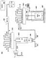
도 6 은 일 실시형태 하에서, SIPM (500) 의 컴포넌트의 서브세트 (총체적으로 SIPM (600) 으로서 불림) 간의 커플링을 나타낸다. SIPM (600) 은 8 개의 입력 A 내지 H 를 포함하는 제 1 혼합 용기 매니폴드 (6121) 를 포함한다. 입력들의 각각은 처리 동작 동안 구성물들을 선택적으로 수용하기 위하여 구성물에 결합된다. 구성물과 제 1 혼합 용기 매니폴드 (6121) 간의 접속의 일례로서, 매니폴드 (6121) 의 입력 A 는 펌프 (604) 를 통해 화학 약품 A 에 접속된다. 펌프 (604) 는 용기를 채우도록 사용된 정량 펌프 (metering pump) 이나 이에 제한되지 않는다; 다른 실시형태는 펌프를 포함하지 않을 수도 있고, 다수의 인라인 펌프들을 포함할 수도 있고/있으며, 상이한 유형의 펌프를 포함할 수도 있다. 일 실시형태의 펌프 (604) 는 각 재료의 체적 비율의 정확한 제어를 고려하는 정량 펌프를 포함하나, 이에 제한되지 않는다. 다른 컴포넌트들 (예를 들어, 밸브, 조절기, 혼합기, 펌프 등) 은 구성물 (예를 들어, 화학 약품 A) 을 유지시키는 컨테이너와 펌프 (604) 간에 및/또는 펌프 (604) 와 매니폴드의 입력 A 간에 인라인으로 접속될 수 있다. 다른 MCSIR 컴포넌트들 및/또는 구성물들이나, 화학 약품 들 (미도시) 은 유사한 방식으로 제 1 혼합 용기 매니폴드 (6121) 의 입력 A 내지 입력 H 에 접속될 수 있다. 제 1 혼합 용기 매니폴드 (6121) 는 상술한 바와 같이 분배 어셈블리의 컴포넌트일 수 있으나, 이에 제한되지 않는다.6 illustrates coupling between a subset of components of SIPM 500 (collectively referred to as SIPM 600) under one embodiment.
SIPM (600) 은 제 1 혼합 용기 매니폴드 (6121) 의 출력에 접속된 입력을 가지는 혼합 용기 (6141) 를 포함한다. 혼합 용기 (6141) 는 그러므로 제 1 혼합 용기 매니폴드 (6121) 로부터 흐르는 구성물들을 수용한다. 일 실시형태의 혼합 용기 (6141) 는 용기 (6141) 내에 조성물이 생성되는 예를 들어, 압력, 온도 및 pH 를 포함한 파라마터의 제어를 고려한다. 혼합 용기 (6141) 는 수용된 구성물들을 교반하거나 흔드는 디바이스를 포함할 수 있다. 혼합 용기 (6141) 는 혼합 용기 (6141) 로부터의 조성물을 흘리도록 역할하는 흐름 메커니즘 (606) 을 포함하거나 결합되거나 접속된다. 일례로서, 흐름 메커니즘 (606) 은 프로세스 (608) 로 또는 프로세스로부터 멀어져 폐기물 (610) 로 향하게 하는 접속들을 포함하고; 다른 라우팅들 (미도시) 도 가능하다. 혼합 용기 (6141) 는 상술한 바와 같이 혼합 어셈블리의 컴포넌트일 수 있으나, 이에 제한되지 않는다.
SIPM (600) 은 8 개의 입력 1-8 을 포함하는 사이트 매니폴드 (6321) 를 포함한다. 하나의 입력 1 은 혼합 용기 (6141) 의 조성물 출력 MIX1 을 수용하도록 접속된다. 사이트 매니폴드 (6321) 의 다른 입력들은 다른 구성물들 및/또는 조성물들을 수용하도록 접속될 수 있다. 예를 들어, 상술한 바와 같이, 사이트 매니폴드 (6321) 의 또다른 입력 2 는 또다른 매니폴드 및/또는 혼합 용기의 조성물 출력 MIX2 를 수용하도록 접속될 수 있다. 게다가, 사이트 매니폴드 (6321) 의 다른 또는 남은 입력 3 내지 입력 8 은 하나 이상의 다른 구성물들 (미도시) 에 결합될 수 있다.
사이트 매니폴드 (6321) 의 출력은 기판 (650) 의 일 영역에 근접하는 흐름 셀 (6421) 에 접속된다. SIPM (600) 은 사이트 매니폴드 (6321) 와 흐름 셀 (6421) 간에 인라인 혼합을 제공하는 부가적 인라인 혼합기 (660) 를 포함한다. 흐름 셀 (6421) 은 매니폴드 (6321) 로부터의 조성물을 수용하고, 처리 동작 동안 기판 영역을 처리하기 위하여 그 조성물을 사용한다. 흐름 셀 (6421) 은 유출물 (폐기물) 을 흐름 셀 (6421) 로부터 멀리 향하게 하는 폐기물 라인 (670) 에 접속된다. 폐기물 라인 (670) 은 흐름 셀 (6421) 로부터 프로세스 유출물을 제거하기 위한 진공 매니폴드 또는 밸브 (미도시) 를 포함할 수 있다. 흐름 셀 (6421) 은 상술한 바와 같이 흐름 셀 어셈블리의 컴포넌트일 수 있으나 이에 제한되지 않는다. 제어기 (602) 는 SIPM (600) 의 컴포넌트들에 결합되고 상술한 바와 같이 처리 동작을 제어한다.The output of the
SIPM (600) 의 일 실시형태는 셀을 통해 흐름을 특성화하는 것보다 폐기물 라인을 통해 그 흐름을 특성화하기 위하여 폐기물 라인 내에 유량계 (FM: flow meter) 를 포함한다. 이것은 다수의 유량 제어기들에 대한 필요성을 제거하고 대신에 단일 솔벤트 시스템에 대한 하나의 유량 제어기만을 요구하며; 다수의 유량 제어기가 다수의 솔벤트 시스템과 함께 사용될 것이다 (예를 들어, 산성 솔벤트, 염기성 솔벤트 및 유기 솔벤트를 갖는 시스템에서 3 개의 유량 제어기가 사용된다).One embodiment of
분배 어셈블리, 혼합 용기 매니폴드, 혼합 어셈블리, 흐름 셀 어셈블리, 및 흐름 셀을 포함한 SIPM 의 컴포넌트들은 상술한 바와 같이 수와 구성에서 변화한다. 이들 컴포넌트들은 예를 들어, 밸브, 튜빙 (tubing) 이나 도관, 분배 펌프, 흐름 조절기, 압력 조절기, 및 제어기를 포함하는 다양한 다른 컴포넌트들 및/또는 재료들을 이용하여 결합되거나 접속된다. 이들 다른 컴포넌트들 및/또는 재료들은 구성 및 처리 동작에 적절하게 기술분야에 공지된 컴포넌트들 및/또는 재료들을 포함한다.The components of the SIPM, including the dispensing assembly, mixing vessel manifold, mixing assembly, flow cell assembly, and flow cell, vary in number and configuration as described above. These components are coupled or connected using various other components and / or materials including, for example, valves, tubing or conduits, dispensing pumps, flow regulators, pressure regulators, and controllers. These other components and / or materials include components and / or materials known in the art as appropriate for configuration and processing operations.
상술한 SIPM 의 구성은 벌크형 화학 약품들이 혼합 용기 매니폴더를 통해 혼합 용기로 및/또는 사이트 매니폴드를 통해 사이트-분리된 반응기로 향하게 한다. 혼합 용기로 향하게 되는 경우, 제어 시스템은 임의의 조성물에 대한 용액들의 혼합을 가능하게 한다. 용액의 조성물은 혼합 용기들의 각각에 대해 독립적으로 변화될 수 있다. 혼합 용기는 이렇게 형성된 용액의 교반, 가열, 및 pH 제어를 허용하는 방식으로 실시된다. 또한, 이렇게 형성된 용액의 pH 및 온도는 흐름 셀마다 모니터링될 수 있다. 게다가, 사이트 매니폴드를 통한 각 용액의 유량은 독립적으로 변화하기 쉽다.The configuration of SIPM described above directs bulk chemicals to the mixing vessel through the mixing vessel manifold and / or to the site-separated reactor via the site manifold. When directed to the mixing vessel, the control system enables mixing of the solutions to any composition. The composition of the solution can be varied independently for each of the mixing vessels. The mixing vessel is carried out in a manner that allows for stirring, heating, and pH control of the solution thus formed. In addition, the pH and temperature of the so formed solution can be monitored per flow cell. In addition, the flow rate of each solution through the site manifold is likely to change independently.
상술한 바와 같이, 각 매니폴드 (예를 들어, 혼합 용기 매니폴드, 사이트 매니폴드) 는 많은 수의 입력 또는 밸브 (예를 들어, X 개의 입력, 여기서 X 는 임의의 수 1, 2, ...) 를 포함하며, 각 밸브가 상이한 화학 약품 소스에 결합되거나 접속된다. 화학 약품 소스는 예를 들어, 액상, 기상 또는 진공일 수도 있다. 매니폴드는 매니폴드의 입력들에서 수용된 화학 약품이 하나의 공통 경로를 통해 매니폴드를 빠져나가도록 구성된다. 따라서, 그 매니폴드는 X:1 매니폴드라고 불린다. 화학 약품은 매니폴드를 통해 개별적으로 또는 조합적으로 시퀀싱될 수 있다. 조합적으로 시퀀싱되는 경우, 인-라인 혼합기는 균일한 화학 용액을 확보하도록 사용될 수 있다. 체크 밸브는 또한 백스트림, 결과적으로, 화학 약품의 원하지 않는 혼합이 발생하지 않음을 확보하도록 X 개의 화학 약품들의 각각의 입구에서 통합될 수 있다.As mentioned above, each manifold (eg mixing vessel manifold, site manifold) has a large number of inputs or valves (eg, X inputs, where X is any
흐름 셀은 SIPM 의 처리의 흐름 역학을 제어한다. 시퀀스 동안 화학 약품 변경 사이의 데드 볼륨 (dead volume) 을 줄이기 위해서, 일 실시형태의 흐름 셀은 독립적으로 프로세스 및 셀 바디와 직접 병합된 폐기물 경로를 포함한다. 도 7 은 일 실시형태 하에서, 독립적 프로세스 P1/P2 경로 및 폐기물 W 경로를 포함한 흐름 셀 (700) 의 블록도이다. 각 흐름 셀 경로는 밸브 V1 내지 밸브 V4 를 통합하여 프로세스 흐름과 폐기물 흐름을 제어한다. 이들 밸브 V1 내지 밸브 V4 의 사용은 예를 들어, 제 2 경로 P2 가 기판의 처리를 위해 화학 약품을 전달하도록 사용 중에 있는 동안 흐름 셀의 제 1 프로세스 경로 P1 이 정화되게 한다. 이 프로세스 경로 제어는 우수한 타이밍 정확도 (timing accuracy) 를 제공하고 흐름 셀로의 화학 약품의 매우 정밀한 시퀀싱을 가능하게 한다.The flow cell controls the flow dynamics of the processing of the SIPM. To reduce the dead volume between chemical changes during the sequence, the flow cell of one embodiment independently includes a waste path that is directly merged with the process and cell body. FIG. 7 is a block diagram of a
밸브 사용의 일례로서, 흐름 셀의 현재 프로세스 단계의 밸브 구성은 밸브 V1 이 닫히고 밸브 V2 가 개방되어 제 1 화학 약품이 제 1 경로에서 폐기물 출력으로 제거되며, 밸브 V4 가 개방되고 밸브 V3 이 닫혀 제 2 화학 약품이 프로세스 출력을 통해 흐름 셀로 제공된다. 현재의 프로세스 단계의 완료 및 다음의 프로 세스 단계의 개시 시, 밸브들은 제 1 경로 P1 의 화학 약품이 프로세스 출력을 통해 기판에 즉시 도입되나, 제 2 경로의 화학 약품이 제거되고 제 2 경로가 후속적으로 프로세스 시퀀스에서의 다음 화학 약품을 이용하여 준비되도록 전환되거나 재구성된다.As an example of valve use, the valve configuration of the current process stage of the flow cell is such that valve V1 is closed and valve V2 is opened to remove the first chemical to waste output in the first path, valve V4 is opened and valve V3 is closed to 2 Chemicals are delivered to the flow cell through the process outputs. At the completion of the current process step and at the beginning of the next process step, the valves are immediately introduced with chemicals in the first path P1 to the substrate via the process output, but the chemicals in the second path are removed and the second path is followed. Typically converted or reconstituted to be prepared with the next chemical in the process sequence.
일 실시형태의 흐름 셀은 반응기로부터의 프로세스 화학 약품을 수집 및 배출하는 진공 매니폴드를 포함한다. 일 실시형태의 진공 매니폴드는 매니폴드 내에 일정한 압력을 유지시키도록 대기로 벤팅 (venting) 되어, 유속의 우수한 예측가능성을 제공하나, 이에 제한되지 않고 대신에 시스템 구성에 적합하게 진공 소스 또는 압력 소스에 결합될 수 있다.The flow cell of one embodiment includes a vacuum manifold that collects and discharges process chemicals from the reactor. The vacuum manifold of one embodiment is vented to the atmosphere to maintain a constant pressure within the manifold, providing excellent predictability of flow rate, but not limited thereto but instead a vacuum source or pressure source suitable for system configuration. Can be coupled to.
SIPM 의 흐름 셀은 흐름 셀들이 단일체로서 집합적으로 상승 및 하강되게 하는 고정물 (fixture) 에 모두 접속된다. 기판에 대한 흐름 셀의 수직 위치의 제어는 반응기 체적이 동적으로 변경되게 한다. 본 기능의 사용에 대한 일례는 정적 버켓-모드 (static bucket-mode) 처리를 용이하게 하기 위해 흐름 셀을 상승시키는 것, 그리고 방사상 흐름 패턴을 용이하게 하기 위해 흐름 셀을 하강시키는 것이다.The flow cell of the SIPM is all connected to a fixture that causes the flow cells to collectively rise and fall as a unit. Control of the vertical position of the flow cell relative to the substrate causes the reactor volume to change dynamically. One example of the use of this function is to raise the flow cell to facilitate static bucket-mode processing, and to lower the flow cell to facilitate the radial flow pattern.
도 4 를 참조하여 상술한 바와 같이, 흐름 셀은 사이트-분리된 반응기의 상부 표면을 포함하나, 반응기 슬리브는 반응기의 측벽을 포함하고 처리된 기판은 반응기의 저부를 포함한다. 반응기 슬리브는 서비스편의를 제공하도록 사용된 불활성 슬리브이다. 예를 들어, 반응기 슬리브는 오염된 경우나 화학적 양립성을 위해 필요한 슬리브 재료를 포함한 슬리브를 제공하기 위하여 쉽게 교체될 수 있 다. 슬리브는 하나 이상의 다양한 재료를 포함할 수 있는 반응기 블록에 의해 고정된다. 반응기 블록은 또한 실온과 상이한 처리 온도를 제공하도록 그리고 상이한 프로세스들에 적절하게 제어기의 제어 하에서 자동적으로 가열되고/가열되거나 냉각될 수 있다.As described above with reference to FIG. 4, the flow cell comprises the top surface of the site-separated reactor, but the reactor sleeve comprises the sidewalls of the reactor and the treated substrate comprises the bottom of the reactor. The reactor sleeve is an inert sleeve used to provide a service convenience. For example, the reactor sleeve can be easily replaced to provide a sleeve that includes the sleeve material needed for contamination or chemical compatibility. The sleeve is secured by a reactor block that may include one or more various materials. The reactor block may also be automatically heated and / or cooled to provide a processing temperature different from room temperature and under the control of the controller as appropriate for the different processes.
MCSIR 은 또한 처리를 진행 중인 기판을 안전하게 하는 척 또는 스테이지를 포함한다. 척은 진공, 정전기, 및/또는 기계적 클램핑을 포함하나 이에 제한되지 않는, 기판을 안전하게 하는 하나 이상의 다양한 메커니즘을 포함할 수 있다. 반응기 블록과 유사하게, 척은 또한 제어기의 제어 하에서 자동적으로 가열되고/가열되거나 냉각될 수 있다. 척은 반응기 어셈블리로부터 기판을 도입하고 회수하는 로봇의 효과적인 사용을 가능하게 하도록 기계적으로 구동될 수 있다.The MCSIR also includes a chuck or stage that secures the substrate being processed. The chuck may include one or more of various mechanisms for securing the substrate, including but not limited to vacuum, electrostatic, and / or mechanical clamping. Similar to the reactor block, the chuck can also be automatically heated and / or cooled under the control of a controller. The chuck can be mechanically driven to enable effective use of the robot to introduce and retrieve the substrate from the reactor assembly.
일 실시형태의 MCSIR 의 모든 컴포넌트들을 통과하는 구성물들에 대한 흐름 제어는 MCSIR 의 접속들에 걸친 압력을 변경함으로써 달성된다. 각각 적어도 하나의 튜빙 접속 및/또는 하나 이상의 정밀한 오리피스나 밸브를 포함할 수 있는 접속은 구성물 및 의도된 프로세스 시퀀스의 구성 파라미터에 대한 MCSIR 에 걸쳐 매칭된다. MCSIR 의 접속은 임의의 실제 사용 전에 교정되고, 교정 커브는 각 접속마다 데이터베이스에 저장된다. 제어기는 처리 동작 동안 구성물 흐름을 제어 시에 교정의 정보를 이용한다.Flow control for the components passing through all components of the MCSIR in one embodiment is achieved by changing the pressure across the connections of the MCSIR. Connections, which may each include at least one tubing connection and / or one or more precise orifices or valves, are matched across the MCSIR for the configuration and configuration parameters of the intended process sequence. The connections of the MCSIR are calibrated before any actual use, and calibration curves are stored in the database for each connection. The controller uses the information of the calibration in controlling the component flow during processing operations.
MCSIR 의 기판 처리는 상술한 바와 같이 기판의 국소화된 영역에 대해 조합형 처리 및 종래의 풀-웨이퍼 처리의 병렬 통합을 포함한다. MCSIR 의 실시형태는 상술한 바와 같이 제어기 (예를 들어, MCSIR (400) 의 제어기 (402) (도 4), MCSIR (500) 의 제어기 (502) (도 5), MCSIR (600) 의 제어기 (602) (도 6)) 의 제어 하에서 처리 동작을 지원한다. 제어기는 호스트 MCSIR 의 다양한 컴포넌트들의 동작을 제어하는 여러가지의 데이터베이스 또는 표의 정보를 이용하는 하나 이상의 프로그램 또는 알고리즘들을 실행하는 프로세서를 포함하고; 그 데이터베이스 또는 표 (미도시) 는 제어기 프로세서에 결합되고 제어기의 컴포넌트이고/컴포넌트이거나 MCSIR 및/또는 호스트 처리 시스템의 다른 컴포넌트들 사이에 분포될 수 있다.Substrate processing of the MCSIR includes parallel integration of combined processing and conventional full-wafer processing for localized areas of the substrate as described above. Embodiments of the MCSIR include a controller (e.g., controller 402 (FIG. 4) of
일 실시형태의 제어기는 프로세스 시퀀스에 대한 전체 컴퓨터 제어/자동화를 제공한다. 반응기들의 각각은 대부분 프로세스 파라미터에 대해서 독립적으로 제어될 수 있으나, 온도와 반응기 체적과 같은 일부 프로세스 파라미터는 모든 사이트들에 대해 광역적이다. 상이한 시퀀스가 상이한 반응기에 사용되고 광역적 파라미터가 변경되는 경우, 제어기는 프로세스 시퀀스가 모든 반응기들에 걸쳐 올바르게 실행하도록 프로세스 단계의 동기화를 가능하게 한다. 프로세스 동기화에 덧붙여, 제어기는 프로세스 단계가 온도와 같은 파라미터의 특정 목표값을 충족한 시스템을 개시하게 하는 프로세스 시퀀스 트리거를 가능하게 한다. 이들 2 개의 성능은 프로세스 시퀀스가 실행될 수 있는 정확성 및 정밀도를 더 개선한다.The controller of one embodiment provides full computer control / automation for the process sequence. Each of the reactors can be controlled independently for most process parameters, but some process parameters, such as temperature and reactor volume, are global for all sites. If different sequences are used for different reactors and global parameters are changed, the controller enables synchronization of process steps so that the process sequence runs correctly across all reactors. In addition to process synchronization, the controller enables a process sequence trigger that allows a process step to initiate a system that meets a specific target value of a parameter such as temperature. These two capabilities further improve the accuracy and precision with which a process sequence can be executed.
기판 처리 동작을 제어하는 일반적 예로서, 도 8 은 기판의 혼합-모드 처리의 흐름도이다. 다수의 생 화학 약품들로부터 용액들이 생성된다 (802). 조성물 및 파라미터는 조합 방식으로 변화되고 다수의 용액들 중 상이한 용액들 사이에서 독립적으로 제어된다. 화학 약품 및 용액들은 기판 상에 분배되고 (804), 분배는 기판의 전체 표면 상에 화학 약품의 분배 및 다수의 용액의 분배를 통합하는 것을 포함한다. 다수의 용액의 분배는 하나 이상의 분배된 용액 및 기판의 영역들의 하나 이상의 세트들 사이의 흐름을 독립적으로 변화시키는 것을 포함한다.As a general example of controlling substrate processing operations, FIG. 8 is a flow chart of mixed-mode processing of a substrate. Solutions are produced from a number of live chemicals (802). Compositions and parameters are varied in a combinatorial fashion and controlled independently between different solutions of a plurality of solutions. The chemicals and solutions are dispensed on the
MCSIR 제어기를 이용하여 처리 동작을 제어하는 보다 구체적인 예는 다음과 같다. 동작은 일반적으로 오퍼레이터가 시퀀스를 선택하고/선택하거나 설정하고 그 시퀀스에 적절한 라이브러리를 선택하고/선택하거나 설정할 때 시작된다. 기판 (예를 들어, 웨이퍼) 은 로딩되고, 라이브러리는 사전-스테이징 (pre-stage) 된다. 선택된 처리 시퀀스는 이후 실행된다. 선택된 시퀀스의 실행에 이어서, 웨이퍼는 언로딩되고 시스템은 플러싱 (flushing) 된다.A more specific example of controlling the processing operation using the MCSIR controller is as follows. The operation generally begins when the operator selects and / or sets the sequence and selects and / or sets the appropriate library for that sequence. The substrate (eg wafer) is loaded and the library is pre-stage. The selected processing sequence is then executed. Following execution of the selected sequence, the wafer is unloaded and the system is flushed.
시퀀스의 설정은 구성물이나 화학 약품 시퀀싱 및 연관된 파라미터들을 정의하는 것을 포함한다. 화학 약품 시퀀싱의 정의는 예를 들어, 하나 이상의 화학 약품 유형, 흐름 시간, 유량, 전하, 적심 (soak), 플러싱 시간, 및 프로세스 온도를 정의하는 것을 포함한다. 일 실시형태의 MCSIR 의 각 흐름 셀을 통한 유량이 거의 동일한 값이면서, 직렬 방식으로 그 유량이 변화될 수 있다. 흐름 시간, 적심 시간, 플러싱 시간은 MCSIR 에 걸쳐 변화될 수 있다. 시퀀싱은 상술한 바와 같이 예를 들어, 하나 이상의 인라인 혼합기들 또는 본 명세서에 기술된 다른 혼합 기술이나 컴포넌트들을 통한 화학 약품으로 혼합을 포함할 수 있다.Setting up a sequence includes defining a component or chemical sequencing and associated parameters. Definition of chemical sequencing includes, for example, defining one or more chemical type, flow time, flow rate, charge, soak, flush time, and process temperature. While the flow rate through each flow cell of the MCSIR of one embodiment is about the same value, the flow rate can be varied in a serial manner. Flow time, wetting time and flushing time can be varied over the MCSIR. Sequencing can include mixing, for example, with chemical through one or more inline mixers or other mixing techniques or components described herein.
일 실시형태의 처리 시퀀스를 위한 라이브러리를 설정하는 것은 하나 이상의 혼합물 내의 각 화학 약품의 농도, 각 용액의 온도 및 pH, 및 각 혼합물의 전체 체 적을 설정하는 것을 포함한다 (시퀀스 정보로부터 디폴트 값은 제공된다). 라이브러리의 설정은 부가적이다.Setting up a library for a treatment sequence of one embodiment includes setting the concentration of each chemical in one or more mixtures, the temperature and pH of each solution, and the total volume of each mixture (the default values from the sequence information provide do). The configuration of the library is additional.
웨이퍼 로딩은 웨이퍼 크기를 정의하는 것을 포함한다. 라이브러리의 사전-스테이징은 MCSIR 의 혼합 용기를 통해 시퀀싱하는 것과 구체적인 구성물의 각 컴포넌트의 적절한 양을 추가하거나 분배하는 것을 포함한다. 정밀 분배 펌프는 혼합 용기 내로의 개별 구성물을 계량하는데 사용된다. 일 실시형태에서는 +/- 1% 정확도로 10 밀리리터 (㎖) 의 전달이 약 5 초 걸린다. MCSIR 은 첫 번째 구성물과 마지막 구성물의 개시 사이에 미리 특정된 시간 간격 (예를 들어, 1 분) 으로 시차를 둔 개시로 혼합 용기로 개별 구성물을 분배한다. 라이브러리의 사전-스테이징은 스테이지 당 시간 주기 (예를 들어, 15 분) 동안 타깃팅되고; 순차적인 웨이퍼들의 경우, 라이브러리 사전-계획은 프로세스 시퀀스와 함께 병렬로 실행될 수 있다. MCSIR 사전-스테이징은 정밀한 온도 및 pH 제어의 조건 하에서 실시되고, 프로세스 시퀀스에 적절하게 구성물의 통합된 혼합을 포함한다.Wafer loading involves defining wafer size. Pre-stage of the library includes sequencing through the mixing vessel of the MCSIR and adding or dispensing the appropriate amount of each component of the specific construct. Precision dispensing pumps are used to meter individual components into the mixing vessel. In one embodiment, delivery of 10 milliliters (ml) with +/- 1% accuracy takes about 5 seconds. The MCSIR distributes the individual constructs to the mixing vessel with a staggered launch at a pre-specified time interval (eg, 1 minute) between the beginning of the first construct and the last construct. Pre-staging of the library is targeted for a time period per stage (eg, 15 minutes); For sequential wafers, library pre-planning can be executed in parallel with the process sequence. MCSIR pre-staging is performed under conditions of precise temperature and pH control and includes integrated mixing of the components as appropriate to the process sequence.
선택된 프로세스 시퀀스의 실행은 시퀀스의 개시, 및 선택된 시퀀스의 모든 정의된 프로세스들의 완료를 포함한다. 프로세스 시퀀스 실행의 데이터는 작동자 또는 다른 사용자에 의해 특정된 바와 같이 기록된다. 기판 (예를 들어, 웨이퍼) 은 프로세스 시퀀스의 완료 시에 언로딩된다. 기판의 제거에 이어서, MCSIR 는 프로세스 유출물 및/또는 미사용 구성물들을 MCSIR 의 컴포넌트들로부터 제거하도록 플러싱된다. MCSIR 은 이후 가스 (예를 들어, 질소) 를 이용하여 가압되고 후속 프로세스 시퀀스가 개시되기 전까지 가압된 상태로 유지된다.Execution of the selected process sequence includes initiation of the sequence and completion of all defined processes of the selected sequence. Data of the process sequence execution is recorded as specified by an operator or other user. The substrate (eg wafer) is unloaded upon completion of the process sequence. Following removal of the substrate, the MCSIR is flushed to remove process effluent and / or unused components from the components of the MCSIR. The MCSIR is then pressurized with a gas (eg nitrogen) and remains pressurized until a subsequent process sequence is initiated.
프로세스 시퀀싱의 일례로서, MCSIR 은 상술한 SIPM 을 이용하여 기판의 영역 내에 사이트-분리된 성막을 포함하는 처리를 지원한다. 어떤 재료의 성막은 2 개의 화학 약품이 혼합되고 상승된 온도에서 웨이퍼 상에 분배되는 것을 요구한다. 성막은 정적 또는 버킷 모드 반응기 내에서 달성되어야 한다. 또한, 화학 약품들은 습기에 노출될 수 없다. 마지막으로, 화학 약품들은 혼합 시 상승된 온도에서 불안정하지만, 혼합되지 않을 경우는 안정적이다. MCSIR 은 현존 프로세스로 본 성막의 효율적인 통합을 달성함에 있어서 중요한 본 시퀀스의 각 단계의 타이밍에 대한 정확한 제어를 가능하게 한다. 다음의 예에서 제공된 파라미터들은 단지 예로서 제공되고 이들 파라미터들 하에서만의 처리에 대해서 MCSIR 을 제한하도록 의도되지 않는다.As an example of process sequencing, MCSIR uses a SIPM as described above to support processing involving site-separated deposition within the area of the substrate. Deposition of certain materials requires the two chemicals to be mixed and dispensed on the wafer at elevated temperature. Deposition should be accomplished in a static or bucket mode reactor. In addition, chemicals cannot be exposed to moisture. Finally, chemicals are unstable at elevated temperatures when mixed, but stable when not mixed. MCSIR enables precise control of the timing of each step of the present sequence, which is important in achieving efficient integration of the present deposition into existing processes. The parameters provided in the following examples are provided by way of example only and are not intended to limit the MCSIR for processing only under these parameters.
상술한 MCSIR 을 이용한 성막을 실행하기 위하여, 상기 도 4 내지 도 6 을 참조하면, 동작은 혼합 용기 매니폴드를 통해 혼합 용기로 화학 약품 A 를 분배함으로써 시작한다. 화학 약품 A 의 온도는 원하는 프로세스 온도까지 상승되고, 화학 약품 A 가 프로세스 온도에 도달하는 때, 제어기는 혼합 용기로 화학 약품 B 의 분배를 트리거링한다. 또한, 2 개의 화학 약품의 기계적 혼합은 혼합 용기 내에서 개시된다.In order to perform the deposition using the MCSIR described above, referring to FIGS. 4 to 6 above, the operation begins by dispensing chemical A into the mixing vessel through the mixing vessel manifold. The temperature of chemical A is raised to the desired process temperature, and when chemical A reaches the process temperature, the controller triggers the dispensing of chemical B into the mixing vessel. In addition, mechanical mixing of the two chemicals is initiated in the mixing vessel.
화학 약품 A 및 화학 약품 B 의 용액의 온도는 이후 사전-특정된 프로세스 온도까지 상승된다. 가열 주기 동안, 기판은 로봇 암 위로 인터페이스에 의해 이동되고 기판 척은 프로세스 온도까지 예열된다. 기판은 용액이 고온 웨이퍼 척 위로 기판이 로딩되는 프로세스 온도에 도달할 때까지 로봇 암 위에 남아 있는 다. 웨이퍼는 위치 내로 구동되고 약 10㎜ 인 높이의 반응기를 이용하여 기판 상에 용액이 분배된다.The temperature of the solutions of Chemical A and Chemical B is then raised to the pre-specified process temperature. During the heating cycle, the substrate is moved by the interface over the robot arm and the substrate chuck is preheated to the process temperature. The substrate remains on the robotic arm until the solution reaches the process temperature at which the substrate is loaded onto the hot wafer chuck. The wafer is driven into position and the solution dispensed onto the substrate using a reactor about 10 mm high.
성막의 끝맺음에 있어서, 기판 척은 능동적으로 냉각되고 반응기 높이는 반응 용액의 배출과 함께 0.25㎜ 까지 감소된다. 용액의 배출과 기판의 냉각 시, 제 2 용액은 흐름 모드에서 반응기로 도입되어 표면의 잔류 화학 약품을 린싱한다. 웨이퍼는 이후 반응기로부터 회수되고 로봇형 인터페이스를 통해 리턴된다.At the end of the deposition, the substrate chuck is actively cooled and the reactor height is reduced to 0.25 mm with the discharge of the reaction solution. Upon exiting the solution and cooling the substrate, the second solution is introduced into the reactor in flow mode to rinse the residual chemical on the surface. The wafer is then withdrawn from the reactor and returned through the robotic interface.
일 실시형태의 MCSIR 은 셀 어셈블리의 반응기들과 타깃 기판의 하나 이상의 영역 간에 시일의 사용을 포함한다. 일 실시형태의 시일 시스템 및 방법은 2 유형의 시일을 포함할 수 있다. 제 1 유형의 시일은 하나 이상의 콘택 시일을 포함하나 제 2 유형의 시일은 시일링 유체를 이용하여 형성된 유체역학적 (hydrodynamic) 배리어의 사용을 포함한다. 이들 시일링 시스템의 각각은 2006 년 06 월 06 일자로 출원된 미국 특허 출원 번호 제 11/448,369 호에서 상세히 기술되어 있다.The MCSIR of one embodiment involves the use of a seal between the reactors of the cell assembly and one or more regions of the target substrate. The seal system and method of one embodiment may include two types of seals. The first type of seal comprises one or more contact seals while the second type of seal includes the use of a hydrodynamic barrier formed using a sealing fluid. Each of these sealing systems is described in detail in US patent application Ser. No. 11 / 448,369, filed June 06, 2006.
도 9 는 일 실시형태 하에서, 기판을 안전하게 할 수 있는 스테이지 또는 척 (904) 에 메이팅된 흐름 셀 어셈블리 (906) 를 포함하는 MCSIR (900) 을 나타낸다. MCSIR (900) 은 플로우팅 반응기 슬리브 또는 벽 (910) 을 포함한다. 플로우팅 반응기 슬리브 (910) 는 셀 어셈블리 (906) 의 반응기 블록의 각 흐름 셀 (908) 내에 플로우팅하거나 동적으로 위치가능하도록 구성된다. 플로우팅 슬리브 (910) 를 포함하는 흐름 셀 (908) 의 조합은 이로써 기판의 국소화된 표면에 (플로우팅 슬리브 (910) 에 의해 형성된) 각 반응기 에지 표면 (912) 에 대한 개별적인 컴플라이언스 (compliance) 를 제공하는 흐름 셀 (908) 을 형성한다.9 illustrates an
반응기 블록 (906) 의 흐름 셀 (908) 내부의 각 반응기 슬리브 (910) 에 대한 컴플라이언스는 일 실시형태에서 O-링인 외부 메커니즘에 의해 제어되고 제공될 수 있으나, 이에 제한되지 않는다. 흐름 셀 (908) 내의 각 반응기 슬리브 (910) 의 컴플라이언스는 또한 슬리브 벽으로 직접적으로 통합된 만곡형 (flexure-type) 메커니즘에 의해 제공될 수 있다. 반응기 슬리브 컴플라이언스 메커니즘들의 각각은 이하에서 상세히 기술된다. 각 흐름 셀 (908) 의 플로우팅 슬리브 (910) 의 사용은 오염되거나 그렇지 않으면 반응기 내의 계속적인 사용에 부적합하게 될 수 있는 개별 반응기 벽의 교체를 고려한다. 게다가, 플로우팅 슬리브 (910) 에 의해 제공된 반응기 블록 (906) 내의 각 흐름 셀 (908) 의 플로우팅은 각 반응기에 대해 시일이 달성되는 여전히 높은 가능성을 제공하면서 반응기 컴포넌트의 보다 큰 제조 허용오차를 허용하게 한다.Compliance for each
일 실시형태의 시스템은 진공을 사용하여 상술한 바와 같이 제 3 의 시일을 제공한다. 진공은 일련의 진공 채널 (900V) 들을 경유 또는 반응기 블록 (906) 을 통해 제공된다. 진공은 처리된 표면과 접촉하도록 구성되는, 제 3 시일에 의해 효과적인 시일링을 확보하도록 표면 시일 (900FS) 과 결합하여 작용한다. 본 표면 시일 (900FS) 은 그러므로 진공을 이용하거나 대안적으로 공압력 (pneumatic force) 을 이용하여 주변 시일을 확립한다.The system of one embodiment uses a vacuum to provide a third seal as described above. Vacuum is provided via a series of
일 실시형태의 분리된 반응기 챔버 (908) 의 외부의 플레넘 (plenum) 영역은 가압될 수 있다. 가압화는 예를 들어, 각각 분리된 반응기 챔버 (908) 의 밖으 로 재료의 누설을 방지하도록 사용된다. 또한, 플레넘을 가압하고 이후 시간에 따라 압력 강하를 측정하는 것은 플로우팅 슬리브 (910) 의 시일링 성능의 모니터링을 고려한다. 또한, 플레넘의 가압화는 분리된 반응기 챔버 (908) 로부터의 잠재적인 유독 화합물의 방출 또는 무제어된 벤팅의 기회를 방지하거나 최소화한다.The plenum region outside of the
상술한 접촉 시일링 시스템에 대한 대안으로서 본 명세서에서 유체역학적 시일링 시스템으로서 불리는 제 2 유형의 시일은 흐름 셀 어셈블리의 반응기들 사이의 유체역학적 배리어를 형성하여 시일링 유체를 이용함으로써 반응기 내용물을 포함한 시일링 유체를 이용한다. 유체역학적 배리어는 하나 이상의 종래의 접촉 시일을 대신한다.As an alternative to the contact sealing system described above, a second type of seal, referred to herein as a hydrodynamic sealing system, includes reactor contents by forming a hydrodynamic barrier between the reactors of the flow cell assembly to utilize the sealing fluid. Sealing fluid is used. The hydrodynamic barrier replaces one or more conventional contact seals.
도 10 은 일 실시형태 하에서, 유체역학적 시일링 시스템 (1000) 을 나타낸다. 유체역학적 시일링 시스템 (1000) 은 시일링 유체 (1010) 를 이용하여 얼마간의 인접한 반응기들 (1008AA 및 1008AB) 로부터 흐름 셀 어셈블리의 각 반응기 (1008) 를 분리시키는 1 차적 한정 (primary containment) 이도록 구성된 유체역학적 배리어를 형성한다. 일 실시형태의 유체역학적 시일링 시스템 (1000) 은 또한 기판의 경계선의 영역의 페이스 시일 (1000FS) 을 포함한다. 페이스 시일 (1000FS) 은 기판 (1002) 의 전체 영역을 대략 캡슐화하고 반응종의 2 차적인 한정을 제공한다. 시일링 유체 (1010) 는 하나 이상의 반응기들 (1008, 1008AA, 1008AB) 의 반응에 대해 불활성이어서 시일링 유체 (1010) 는 임의의 반응기 (1008, 1008AA, 1008AB) 중 어느 반응에 대해서도 오염을 유도하지 않는다.10 shows a hydrodynamic sealing system 1000, under one embodiment. Hydrodynamic sealing system 1000 is configured to be a primary containment that separates each
유체역학적 시일은 기판 접촉 없이 기판 (1002) 의 표면 위에 반응기들을 위치시킴으로써 제공된다. 기판 (1002) 에 근접하게 반응기들을 위치시키는 것은 반응기들의 저부와 기판 (1002) 사이의 제어된 갭 (1020) 의 형성을 초래한다. 반응기들은 그러므로 기판과 물리적으로 접촉되지 않는다. 제어된 갭 (1020) 의 범위는 시일링 유체 (1010) 및/또는 반응기들 (1008, 1008AA, 1008AB) 의 반응물의 특성 (예를 들어, 유체 구성물, 소수성 (hydrophobicity), 친수성 (hydrophilicity), 반응성, 점성 등) 을 통해 변조될 수 있다.Hydrodynamic seals are provided by placing the reactors on the surface of the
유체역학적 베어링 매커니즘은 시일링 유체 (1010) 및 유출물 채널의 개별 압력을 제어함으로써 기판 위의 반응기 (1008) 들의 플로우팅 높이, 이로써 제어된 갭 (1020) 을 제어하나, 이에 제한되지 않는다. 시일링 유체 (1010) 는 경계선 공간 (1004) 또는 반응기 (1008) 의 벽 내의 채널 (1012) 들의 제 1 세트를 통해 유체역학적 시일링 시스템 (1000) 으로 도입된다. 일 실시형태의 채널 (1012) 들의 제 1 세트는 하나의 채널을 포함하나 다른 실시형태는 임의의 수 또는 유형의 채널이나 통로를 포함할 수 있다. 반응 유체 (1018) 는 또한 반응기 (1008) 로 도입되고 반응 유체 (1018) 를 포함한 정적 반응의 기간 동안 반응기 (1008) 내에 함유된다. 시일링 유체 (1010) 는 반응기 (1008) 내에 도입되는 반응 유체 (1018) 를 포함하는 유체역학적 배리어를 형성하도록 역할한다. 일 실시형태에서, 이것은 시일링 유체 (1010) 의 적절한 (예를 들어, 높은) 흐름 및/또는 (예를 들어, 짧은) 프로세스 기간을 선택하여 반응기 (1008) 로부터 도입되는 반응 유체 (1018) 의 아웃-디퓨젼을 제한함으로써 달성될 수 있다. 유체역학적 시일은 그 러므로 시일링 유체 (1010) 에 의해 확립된 근사 경계선들로 반응 유체 (1018) 의 에지-투-에지 흐름을 제한하는 것에 의해 반응기 (1008) 내부에 기판 (1002) 의 특정 지역 또는 영역을 캡슐화한다. 반응의 완료 시, 반응 유체 (1018) 는 (예를 들어, 흡입관을 통해) 반응기 (1008) 로부터 제거되나 이에 제한되지 않는다.The hydrodynamic bearing mechanism controls, but is not limited to, the floating height of the
시일링 유체 (1010) 는 반응기 (1008) 의 경계선 공간 (1004) 내의 채널들의 제 2 세트 (1014) 를 통해 반응 폐기물 (1019) 과 함께 수집된다. 반응기의 경계선 공간 (1004) 의 채널 (1004) 들의 제 2 세트는 시일링 채널로서 정의된 영역 내에서 채널들의 제 1 세트와 채널 (1014) 들이 대응하는 반응기 사이에 위치된다. 일 실시형태의 채널 (1004) 들의 제 2 세트는 하나의 채널을 포함하나 다른 실시형태는 임의의 수 또는 유형의 채널이나 통로를 포함할 수 있다. 일 실시형태의 유체역학적 시일링 시스템은 채널 (1014) 의 제 2 세트를 통해 시일링 유체 (1010) 및/또는 반응 폐기물 (1019) 을 수집하는 진공 소스를 포함한다.The sealing
상술한 유체 역학 시일링 시스템은 반응기의 컴포넌트들이 기판과 직접 물리적 접촉을 갖지 않고 반응기-대-반응기 분리를 제공하고, 그것에 의하여 반응기와의 물리적 접촉에 의해 반응 오염의 가능성을 저감하거나 제거한다. 유체역학적 시일링 시스템은 또한 2 레벨의 한정을 제공하여 환경에 반응물의 누설이 없음을 보장한다.The hydrodynamic sealing system described above provides reactor-to-reactor separation without the components of the reactor having direct physical contact with the substrate, thereby reducing or eliminating the possibility of reaction contamination by physical contact with the reactor. The hydrodynamic sealing system also provides two levels of confinement to ensure that there is no leakage of reactants in the environment.
일 실시형태의 기판 처리는 기판 상에 재료 (예를 들어, 층 또는 구조물을 형성) 를 형성하는 하나 이상의 기판 처리 시스템 및 프로세스에서 사용된다. 본 명세서에서 사용되는 바와 같이 기판 상의 재료의 형성은 기판 재료 상에 직접 적으로 재료를 형성하는 것뿐만 아니라 기판 상에 기 형성된 다른 재료 상에 재료를 형성하는 것 모두를 포함하나, 이에 제한되지 않을 수도 있다. 기판 처리는 매우 저렴하게 기판 상에 매우 작은 (예를 들어, 나노 크기 규모에서) 구조물 및 피쳐의 생성을 가능하게 하고, 이것은 다양한 생성물의 제조 시에 유용할 수 있다. 추가적으로, 기판 처리는 상용 기판 처리 장치 및 방법 (예를 들어, 상용 반도체 처리 장비 및 방법) 에 의해 가능하게 된 하나 이상의 능력을 이용하여 기판 상에 재료를 형성하는 기판 처리의 성능을 용이하게 하고/용이하게 하거나 강화할 수 있다.Substrate processing of one embodiment is used in one or more substrate processing systems and processes for forming material (eg, forming layers or structures) on a substrate. As used herein, the formation of a material on a substrate includes, but is not limited to, both forming a material directly on a substrate material as well as forming a material on another material previously formed on a substrate. It may be. Substrate processing very inexpensively enables the creation of very small (eg, on a nano-scale scale) structures and features on a substrate, which can be useful in the manufacture of various products. Additionally, substrate processing facilitates the performance of substrate processing to form materials on substrates using one or more capabilities enabled by commercial substrate processing apparatus and methods (eg, commercial semiconductor processing equipment and methods) / It can be facilitated or enhanced.
기판 처리는 임의의 크기의 기판을 포함할 수 있다. 예를 들어, 기판 처리는 많은 전자 컴포넌트의 제조 시 사용된 1 제곱 인치 미만인 면적을 갖는 작은 반도체 기판에서 12 인치 (300㎜) 이상의 반도체 기판까지의 처리 시에 사용될 수 있다. 일반적으로, 처리될 수 있는 기판의 크기에 제한이 없다. 예를 들어, 기판 처리는 전자 컴포넌트를 생성하는데 사용된 반도체 기판의 각각 계속되는 보다 큰 생성을 처리하는데 사용될 수 있다. 기판 처리는 또한 평판 패널 디스플레이의 제조 시 사용되는 상대적으로 큰 기판을 처리하는데 사용될 수 있다. 이러한 기판은 약 1 제곱 미터의 크기의 장방형 기판을 포함하나 보다 큰 기판이 사용될 수 있다. 기판 처리는 또한 고정된 폭을 갖는 가요성 기판에 대한 롤-투-롤 처리 애플리케이션에 사용하기 위하여 스케일될 수 있으나 (이론적으로) 길이 제한은 없고 (평판 패널 디스플레이의 제조 시 특히 유용할 수 있는 기판 처리의 방식); 예를 들어, 이러한 기판 롤은 수 백 피트의 길이일 수 있다.Substrate processing can include substrates of any size. For example, substrate processing can be used in processing from small semiconductor substrates having an area less than one square inch used in the manufacture of many electronic components to semiconductor substrates of 12 inches (300 mm) or more. In general, there is no limit to the size of the substrate that can be processed. For example, substrate processing can be used to process each subsequent larger generation of semiconductor substrates used to produce electronic components. Substrate processing can also be used to process relatively large substrates used in the manufacture of flat panel displays. Such substrates include rectangular substrates the size of about one square meter, although larger substrates may be used. Substrate processing can also be scaled for use in roll-to-roll processing applications for flexible substrates having a fixed width but (theoretically) have no length limitations and substrates that can be particularly useful in the manufacture of flat panel displays. Mode of treatment); For example, such substrate rolls can be several hundred feet in length.
기판 처리는 단일 기판 또는 복수의 기판 (예를 들어, 배치 처리) 의 처리 시 사용될 수 있다. 예를 들어, 습식 반도체 처리 시, 단일 기판은 처리될 수 있고, 또한 예를 들어, 13, 25 또는 50 개의 기판의 배치는 단일 시간에 처리될 수 있다. 건식 반도체 처리 및 평판 패널 디스플레이 제조 시, 통상적으로, 단일 기판은 한번에 처리된다.Substrate processing can be used in the processing of a single substrate or a plurality of substrates (eg, batch processing). For example, in wet semiconductor processing, a single substrate can be processed and, for example, a batch of 13, 25 or 50 substrates can be processed in a single time. In dry semiconductor processing and flat panel display fabrication, a single substrate is typically processed at one time.
본 명세서에서 서술한 기판 처리는 습식 처리 및/또는 건식 처리를 포함할 수 있다. 습식 처리에서, 기판은 유체를 이용하여 처리된다. 예를 들어, 기판은 구체적 특성 (예를 들어, 구체적 화학 약품의 조성물) 을 갖는 유체 내에 전체 또는 일부가 침지될 수 있다. 또한, 예를 들어, 유체는 구체적 방식으로 기판 상에 분사될 수 있다. 일 실시형태의 기판 처리에 사용하는 습식 처리는 원하는 처리를 위해 적절하게 임의의 다양한 화학 약품 구성물들을 이용할 수 있다.Substrate treatments described herein can include wet treatments and / or dry treatments. In wet processing, the substrate is processed using a fluid. For example, the substrate may be immersed in whole or in part in a fluid having specific properties (eg, a composition of a specific chemical). Also, for example, the fluid can be sprayed onto the substrate in a specific manner. The wet treatment used in the substrate treatment of one embodiment may utilize any of a variety of chemical components as appropriate for the desired treatment.
건식 처리 (예를 들어, 물리적 기상 증착, 화학적 기상 증착, 플라즈마-강화된 화학적 기상 증착, 및 원자층 증착) 시, 플라즈마 또는 가스는 구체화된 방식으로 기판 표면을 처리하는 기판과의 원하는 상호 작용을 생성하도록 사용된다. 기판 처리에 사용하는 건식 처리는 원하는 처리를 위해 적절하게 불활성 가스 또는 반응성 가스를 이용할 수 있다.In dry processing (eg, physical vapor deposition, chemical vapor deposition, plasma-enhanced chemical vapor deposition, and atomic layer deposition), the plasma or gas is required to interact with the substrate to treat the substrate surface in a materialized manner. Used to generate The dry treatment used for the substrate treatment may use an inert gas or a reactive gas as appropriate for the desired treatment.
임의의 다양한 화학 약품 구성물 또는 다른 반응물 (집합적으로 본 명세서에서 구성물 또는 화학 약품 구성물로서 불림) 은 일 실시형태의 기판 처리 시스템에 의해 기판 처리 및 관련된 프로세스를 달성하도록 사용될 수 있다. 구성물은 액상, 기상 및/또는 액상과 기상의 부분 조합 (예를 들어, 초임계 유체상) 으로 존재할 수 있다. 사용되는 구성물 및 그 농도뿐만 아니라 구성물의 혼합물은 실시될 특정 프로세스 단계(들)에 의존할 것이다. 화학 약품 전달 시스템은 프로세스에 적절하게 화학 약품 구성물에 대한 몰 농도, 온도, 유량 및 압력의 정밀한 제어를 가능하게 할 수 있다. 화학 약품 전달 시스템은 또한 오염의 적절한 여과 및 제어를 제공할 수 있다.Any of a variety of chemical components or other reactants (collectively referred to herein as components or chemical components) may be used to achieve substrate processing and related processes by the substrate processing system of one embodiment. The constituents may be in liquid phase, gas phase and / or partial combination of liquid phase and gas phase (eg supercritical fluid phase). The composition used and its concentration as well as the mixture of components will depend on the particular process step (s) to be performed. The chemical delivery system can enable precise control of the molar concentration, temperature, flow rate and pressure for the chemical composition as appropriate to the process. Chemical delivery systems can also provide appropriate filtration and control of contamination.
기판 처리 시스템에 대해 서술된 실시형태의 상기 설명은 철저히 또는 정확히 개시된 형태로 기판 처리 시스템을 제한하도록 의도되지 않는다. 기판 처리 시스템의 구체적 실시형태 및 실시예가 본 명세서에서 예시적인 목적으로서 기술되지만, 다양한 균등 변경들은 관련 분야의 당업자가 인식하는 것과 같이 기판 처리 시스템의 범위 내에서 가능하다. 본 명세서에서 제공된 기판 처리 시스템의 가르침은 상술한 시스템 및 방법뿐만 아니라 다른 처리 시스템 및 방법에 적용될 수 있다.The above description of the embodiments described for the substrate processing system is not intended to be exhaustive or to limit the substrate processing system to the precisely disclosed form. Although specific embodiments and examples of substrate processing systems are described herein for illustrative purposes, various equivalent modifications are possible within the scope of the substrate processing system as will be appreciated by those skilled in the art. The teachings of the substrate processing system provided herein can be applied to the systems and methods described above as well as other processing systems and methods.
상술한 다양한 실시형태의 요소 및 행위는 추가 실시형태를 제공하도록 결합될 수 있다. 이들 및 다른변경들은 상기 상세한 설명의 견지에서 기판 처리 시스템에 행해질 수 있다.The elements and acts of the various embodiments described above can be combined to provide further embodiments. These and other changes can be made to the substrate processing system in light of the above detailed description.
일반적으로, 다음의 청구범위에 있어서, 사용되는 용어들은 상세한 설명 및 청구범위에서 개시된 특정 실시형태로 기판 처리 시스템을 제한하도록 해석되지 말아야 하고, 청구범위 하에서 동작되는 모든 처리 시스템을 포함하도록 해석되어야 한다.In general, in the following claims, the terms used should not be construed to limit the substrate processing system to the specific embodiments disclosed in the description and claims, but should be construed to cover all processing systems operating under the claims. .
Claims (33)
Translated fromKoreanApplications Claiming Priority (3)
| Application Number | Priority Date | Filing Date | Title |
|---|---|---|---|
| US11/647,881 | 2006-12-29 | ||
| US11/647,881US8011317B2 (en) | 2006-12-29 | 2006-12-29 | Advanced mixing system for integrated tool having site-isolated reactors |
| PCT/US2007/088859WO2008083178A1 (en) | 2006-12-29 | 2007-12-26 | Advanced mixing system for integrated tool having site-isolated reactors |
Publications (2)
| Publication Number | Publication Date |
|---|---|
| KR20090102773A KR20090102773A (en) | 2009-09-30 |
| KR101387877B1true KR101387877B1 (en) | 2014-04-22 |
Family
ID=39582389
Family Applications (1)
| Application Number | Title | Priority Date | Filing Date |
|---|---|---|---|
| KR1020097013507AExpired - Fee RelatedKR101387877B1 (en) | 2006-12-29 | 2007-12-26 | Advanced mixing system for integrated tool having site-isolated reactors |
Country Status (6)
| Country | Link |
|---|---|
| US (4) | US8011317B2 (en) |
| JP (1) | JP2010515273A (en) |
| KR (1) | KR101387877B1 (en) |
| CN (1) | CN101606226B (en) |
| TW (1) | TWI385715B (en) |
| WO (1) | WO2008083178A1 (en) |
Families Citing this family (297)
| Publication number | Priority date | Publication date | Assignee | Title |
|---|---|---|---|---|
| US20110081415A1 (en)* | 2005-03-10 | 2011-04-07 | Taisho Pharmaceutical Co., Ltd | Coating apparatus |
| US8011317B2 (en)* | 2006-12-29 | 2011-09-06 | Intermolecular, Inc. | Advanced mixing system for integrated tool having site-isolated reactors |
| JP5474278B2 (en)* | 2007-02-22 | 2014-04-16 | ピーエスフォー ルクスコ エスエイアールエル | Batch type film forming apparatus for supercritical process and manufacturing method of semiconductor device |
| US9044774B2 (en)* | 2007-12-18 | 2015-06-02 | Intermolecular, Inc. | Vented combinatorial processing cell |
| US8037894B1 (en) | 2007-12-27 | 2011-10-18 | Intermolecular, Inc. | Maintaining flow rate of a fluid |
| US8220502B1 (en)* | 2007-12-28 | 2012-07-17 | Intermolecular, Inc. | Measuring volume of a liquid dispensed into a vessel |
| US9016233B1 (en)* | 2008-04-23 | 2015-04-28 | Intermolecular, Inc. | Volume combinatorial processing chamber |
| US20100075060A1 (en)* | 2008-09-24 | 2010-03-25 | Pravin Narwankar | process tool including plasma spray for carbon nanotube growth |
| JP5060517B2 (en)* | 2009-06-24 | 2012-10-31 | 東京エレクトロン株式会社 | Imprint system |
| JP2011009362A (en)* | 2009-06-24 | 2011-01-13 | Tokyo Electron Ltd | Imprint system, imprinting method, program, and computer storage medium |
| US20130023129A1 (en) | 2011-07-20 | 2013-01-24 | Asm America, Inc. | Pressure transmitter for a semiconductor processing environment |
| US8647446B2 (en) | 2011-12-07 | 2014-02-11 | Intermolecular, Inc. | Method and system for improving performance and preventing corrosion in multi-module cleaning chamber |
| US10714315B2 (en) | 2012-10-12 | 2020-07-14 | Asm Ip Holdings B.V. | Semiconductor reaction chamber showerhead |
| CN103811378B (en)* | 2012-11-14 | 2016-08-03 | 沈阳芯源微电子设备有限公司 | A kind of automatic mobile device of semiconductor manufacturing facility |
| US8893923B2 (en)* | 2012-11-28 | 2014-11-25 | Intermolecular, Inc. | Methods and systems for dispensing different liquids for high productivity combinatorial processing |
| US20140144471A1 (en)* | 2012-11-28 | 2014-05-29 | Intermolecular, Inc. | Contamination Control, Rinsing, and Purging Methods to Extend the Life of Components within Combinatorial Processing Systems |
| US20160376700A1 (en) | 2013-02-01 | 2016-12-29 | Asm Ip Holding B.V. | System for treatment of deposition reactor |
| EP2965349A2 (en)* | 2013-03-06 | 2016-01-13 | Plasma-Therm, Llc | Method and apparatus for plasma dicing a semi-conductor wafer |
| US20140262028A1 (en)* | 2013-03-13 | 2014-09-18 | Intermolecular, Inc. | Non-Contact Wet-Process Cell Confining Liquid to a Region of a Solid Surface by Differential Pressure |
| US9269567B2 (en)* | 2013-12-17 | 2016-02-23 | Intermolecular, Inc. | High productivity combinatorial processing using pressure-controlled one-way valves |
| US20150233008A1 (en)* | 2014-02-13 | 2015-08-20 | Skyworks Solutions, Inc. | Apparatus and methods related to copper plating of wafers |
| US11015245B2 (en) | 2014-03-19 | 2021-05-25 | Asm Ip Holding B.V. | Gas-phase reactor and system having exhaust plenum and components thereof |
| US11267012B2 (en)* | 2014-06-25 | 2022-03-08 | Universal Display Corporation | Spatial control of vapor condensation using convection |
| EP2960059B1 (en) | 2014-06-25 | 2018-10-24 | Universal Display Corporation | Systems and methods of modulating flow during vapor jet deposition of organic materials |
| US11220737B2 (en) | 2014-06-25 | 2022-01-11 | Universal Display Corporation | Systems and methods of modulating flow during vapor jet deposition of organic materials |
| US10941490B2 (en) | 2014-10-07 | 2021-03-09 | Asm Ip Holding B.V. | Multiple temperature range susceptor, assembly, reactor and system including the susceptor, and methods of using the same |
| US10276355B2 (en) | 2015-03-12 | 2019-04-30 | Asm Ip Holding B.V. | Multi-zone reactor, system including the reactor, and method of using the same |
| US11357966B2 (en) | 2015-04-23 | 2022-06-14 | B. Braun Medical Inc. | Compounding device, system, kit, software, and method |
| US10458018B2 (en) | 2015-06-26 | 2019-10-29 | Asm Ip Holding B.V. | Structures including metal carbide material, devices including the structures, and methods of forming same |
| KR102420015B1 (en)* | 2015-08-28 | 2022-07-12 | 삼성전자주식회사 | Shower head of Combinatorial Spatial Atomic Layer Deposition apparatus |
| US10566534B2 (en) | 2015-10-12 | 2020-02-18 | Universal Display Corporation | Apparatus and method to deliver organic material via organic vapor-jet printing (OVJP) |
| US10211308B2 (en) | 2015-10-21 | 2019-02-19 | Asm Ip Holding B.V. | NbMC layers |
| US11139308B2 (en) | 2015-12-29 | 2021-10-05 | Asm Ip Holding B.V. | Atomic layer deposition of III-V compounds to form V-NAND devices |
| US10529554B2 (en) | 2016-02-19 | 2020-01-07 | Asm Ip Holding B.V. | Method for forming silicon nitride film selectively on sidewalls or flat surfaces of trenches |
| US10343920B2 (en) | 2016-03-18 | 2019-07-09 | Asm Ip Holding B.V. | Aligned carbon nanotubes |
| US10367080B2 (en) | 2016-05-02 | 2019-07-30 | Asm Ip Holding B.V. | Method of forming a germanium oxynitride film |
| US11453943B2 (en) | 2016-05-25 | 2022-09-27 | Asm Ip Holding B.V. | Method for forming carbon-containing silicon/metal oxide or nitride film by ALD using silicon precursor and hydrocarbon precursor |
| US9859151B1 (en) | 2016-07-08 | 2018-01-02 | Asm Ip Holding B.V. | Selective film deposition method to form air gaps |
| US10612137B2 (en) | 2016-07-08 | 2020-04-07 | Asm Ip Holdings B.V. | Organic reactants for atomic layer deposition |
| KR102532607B1 (en) | 2016-07-28 | 2023-05-15 | 에이에스엠 아이피 홀딩 비.브이. | Substrate processing apparatus and method of operating the same |
| US9812320B1 (en) | 2016-07-28 | 2017-11-07 | Asm Ip Holding B.V. | Method and apparatus for filling a gap |
| US9887082B1 (en) | 2016-07-28 | 2018-02-06 | Asm Ip Holding B.V. | Method and apparatus for filling a gap |
| CN106971660A (en)* | 2016-10-27 | 2017-07-21 | 北京石油化工学院 | A kind of multifunctional modular experimental provision based on static mixer |
| US11532757B2 (en) | 2016-10-27 | 2022-12-20 | Asm Ip Holding B.V. | Deposition of charge trapping layers |
| US10714350B2 (en) | 2016-11-01 | 2020-07-14 | ASM IP Holdings, B.V. | Methods for forming a transition metal niobium nitride film on a substrate by atomic layer deposition and related semiconductor device structures |
| KR102546317B1 (en) | 2016-11-15 | 2023-06-21 | 에이에스엠 아이피 홀딩 비.브이. | Gas supply unit and substrate processing apparatus including the same |
| KR102762543B1 (en) | 2016-12-14 | 2025-02-05 | 에이에스엠 아이피 홀딩 비.브이. | Substrate processing apparatus |
| US11581186B2 (en) | 2016-12-15 | 2023-02-14 | Asm Ip Holding B.V. | Sequential infiltration synthesis apparatus |
| US11447861B2 (en) | 2016-12-15 | 2022-09-20 | Asm Ip Holding B.V. | Sequential infiltration synthesis apparatus and a method of forming a patterned structure |
| KR102700194B1 (en)* | 2016-12-19 | 2024-08-28 | 에이에스엠 아이피 홀딩 비.브이. | Substrate processing apparatus |
| US10269558B2 (en) | 2016-12-22 | 2019-04-23 | Asm Ip Holding B.V. | Method of forming a structure on a substrate |
| US11390950B2 (en) | 2017-01-10 | 2022-07-19 | Asm Ip Holding B.V. | Reactor system and method to reduce residue buildup during a film deposition process |
| US10468261B2 (en) | 2017-02-15 | 2019-11-05 | Asm Ip Holding B.V. | Methods for forming a metallic film on a substrate by cyclical deposition and related semiconductor device structures |
| US10529563B2 (en) | 2017-03-29 | 2020-01-07 | Asm Ip Holdings B.V. | Method for forming doped metal oxide films on a substrate by cyclical deposition and related semiconductor device structures |
| US10770286B2 (en) | 2017-05-08 | 2020-09-08 | Asm Ip Holdings B.V. | Methods for selectively forming a silicon nitride film on a substrate and related semiconductor device structures |
| US12040200B2 (en) | 2017-06-20 | 2024-07-16 | Asm Ip Holding B.V. | Semiconductor processing apparatus and methods for calibrating a semiconductor processing apparatus |
| US11306395B2 (en) | 2017-06-28 | 2022-04-19 | Asm Ip Holding B.V. | Methods for depositing a transition metal nitride film on a substrate by atomic layer deposition and related deposition apparatus |
| KR20190009245A (en) | 2017-07-18 | 2019-01-28 | 에이에스엠 아이피 홀딩 비.브이. | Methods for forming a semiconductor device structure and related semiconductor device structures |
| US11018002B2 (en) | 2017-07-19 | 2021-05-25 | Asm Ip Holding B.V. | Method for selectively depositing a Group IV semiconductor and related semiconductor device structures |
| US11374112B2 (en) | 2017-07-19 | 2022-06-28 | Asm Ip Holding B.V. | Method for depositing a group IV semiconductor and related semiconductor device structures |
| US10541333B2 (en) | 2017-07-19 | 2020-01-21 | Asm Ip Holding B.V. | Method for depositing a group IV semiconductor and related semiconductor device structures |
| US10590535B2 (en) | 2017-07-26 | 2020-03-17 | Asm Ip Holdings B.V. | Chemical treatment, deposition and/or infiltration apparatus and method for using the same |
| TWI815813B (en) | 2017-08-04 | 2023-09-21 | 荷蘭商Asm智慧財產控股公司 | Showerhead assembly for distributing a gas within a reaction chamber |
| US10770336B2 (en) | 2017-08-08 | 2020-09-08 | Asm Ip Holding B.V. | Substrate lift mechanism and reactor including same |
| US10692741B2 (en) | 2017-08-08 | 2020-06-23 | Asm Ip Holdings B.V. | Radiation shield |
| US11769682B2 (en) | 2017-08-09 | 2023-09-26 | Asm Ip Holding B.V. | Storage apparatus for storing cassettes for substrates and processing apparatus equipped therewith |
| US11139191B2 (en) | 2017-08-09 | 2021-10-05 | Asm Ip Holding B.V. | Storage apparatus for storing cassettes for substrates and processing apparatus equipped therewith |
| US11830730B2 (en) | 2017-08-29 | 2023-11-28 | Asm Ip Holding B.V. | Layer forming method and apparatus |
| KR102491945B1 (en) | 2017-08-30 | 2023-01-26 | 에이에스엠 아이피 홀딩 비.브이. | Substrate processing apparatus |
| US11295980B2 (en) | 2017-08-30 | 2022-04-05 | Asm Ip Holding B.V. | Methods for depositing a molybdenum metal film over a dielectric surface of a substrate by a cyclical deposition process and related semiconductor device structures |
| US11056344B2 (en) | 2017-08-30 | 2021-07-06 | Asm Ip Holding B.V. | Layer forming method |
| US10658205B2 (en) | 2017-09-28 | 2020-05-19 | Asm Ip Holdings B.V. | Chemical dispensing apparatus and methods for dispensing a chemical to a reaction chamber |
| US10403504B2 (en) | 2017-10-05 | 2019-09-03 | Asm Ip Holding B.V. | Method for selectively depositing a metallic film on a substrate |
| US10923344B2 (en) | 2017-10-30 | 2021-02-16 | Asm Ip Holding B.V. | Methods for forming a semiconductor structure and related semiconductor structures |
| US11022879B2 (en) | 2017-11-24 | 2021-06-01 | Asm Ip Holding B.V. | Method of forming an enhanced unexposed photoresist layer |
| CN111344522B (en) | 2017-11-27 | 2022-04-12 | 阿斯莫Ip控股公司 | Including clean mini-environment device |
| WO2019103613A1 (en) | 2017-11-27 | 2019-05-31 | Asm Ip Holding B.V. | A storage device for storing wafer cassettes for use with a batch furnace |
| US10872771B2 (en) | 2018-01-16 | 2020-12-22 | Asm Ip Holding B. V. | Method for depositing a material film on a substrate within a reaction chamber by a cyclical deposition process and related device structures |
| TWI799494B (en) | 2018-01-19 | 2023-04-21 | 荷蘭商Asm 智慧財產控股公司 | Deposition method |
| KR102695659B1 (en) | 2018-01-19 | 2024-08-14 | 에이에스엠 아이피 홀딩 비.브이. | Method for depositing a gap filling layer by plasma assisted deposition |
| US11081345B2 (en) | 2018-02-06 | 2021-08-03 | Asm Ip Holding B.V. | Method of post-deposition treatment for silicon oxide film |
| US10896820B2 (en) | 2018-02-14 | 2021-01-19 | Asm Ip Holding B.V. | Method for depositing a ruthenium-containing film on a substrate by a cyclical deposition process |
| WO2019158960A1 (en) | 2018-02-14 | 2019-08-22 | Asm Ip Holding B.V. | A method for depositing a ruthenium-containing film on a substrate by a cyclical deposition process |
| US10731249B2 (en) | 2018-02-15 | 2020-08-04 | Asm Ip Holding B.V. | Method of forming a transition metal containing film on a substrate by a cyclical deposition process, a method for supplying a transition metal halide compound to a reaction chamber, and related vapor deposition apparatus |
| KR102636427B1 (en) | 2018-02-20 | 2024-02-13 | 에이에스엠 아이피 홀딩 비.브이. | Substrate processing method and apparatus |
| US10975470B2 (en) | 2018-02-23 | 2021-04-13 | Asm Ip Holding B.V. | Apparatus for detecting or monitoring for a chemical precursor in a high temperature environment |
| US11473195B2 (en) | 2018-03-01 | 2022-10-18 | Asm Ip Holding B.V. | Semiconductor processing apparatus and a method for processing a substrate |
| US11629406B2 (en) | 2018-03-09 | 2023-04-18 | Asm Ip Holding B.V. | Semiconductor processing apparatus comprising one or more pyrometers for measuring a temperature of a substrate during transfer of the substrate |
| US11114283B2 (en) | 2018-03-16 | 2021-09-07 | Asm Ip Holding B.V. | Reactor, system including the reactor, and methods of manufacturing and using same |
| KR102646467B1 (en) | 2018-03-27 | 2024-03-11 | 에이에스엠 아이피 홀딩 비.브이. | Method of forming an electrode on a substrate and a semiconductor device structure including an electrode |
| US11088002B2 (en) | 2018-03-29 | 2021-08-10 | Asm Ip Holding B.V. | Substrate rack and a substrate processing system and method |
| US11230766B2 (en) | 2018-03-29 | 2022-01-25 | Asm Ip Holding B.V. | Substrate processing apparatus and method |
| KR102600229B1 (en) | 2018-04-09 | 2023-11-10 | 에이에스엠 아이피 홀딩 비.브이. | Substrate supporting device, substrate processing apparatus including the same and substrate processing method |
| US12025484B2 (en) | 2018-05-08 | 2024-07-02 | Asm Ip Holding B.V. | Thin film forming method |
| TWI811348B (en) | 2018-05-08 | 2023-08-11 | 荷蘭商Asm 智慧財產控股公司 | Methods for depositing an oxide film on a substrate by a cyclical deposition process and related device structures |
| US12272527B2 (en) | 2018-05-09 | 2025-04-08 | Asm Ip Holding B.V. | Apparatus for use with hydrogen radicals and method of using same |
| KR102596988B1 (en) | 2018-05-28 | 2023-10-31 | 에이에스엠 아이피 홀딩 비.브이. | Method of processing a substrate and a device manufactured by the same |
| US11718913B2 (en) | 2018-06-04 | 2023-08-08 | Asm Ip Holding B.V. | Gas distribution system and reactor system including same |
| TWI840362B (en) | 2018-06-04 | 2024-05-01 | 荷蘭商Asm Ip私人控股有限公司 | Wafer handling chamber with moisture reduction |
| US11286562B2 (en) | 2018-06-08 | 2022-03-29 | Asm Ip Holding B.V. | Gas-phase chemical reactor and method of using same |
| KR102568797B1 (en) | 2018-06-21 | 2023-08-21 | 에이에스엠 아이피 홀딩 비.브이. | Substrate processing system |
| US10797133B2 (en) | 2018-06-21 | 2020-10-06 | Asm Ip Holding B.V. | Method for depositing a phosphorus doped silicon arsenide film and related semiconductor device structures |
| TWI873894B (en) | 2018-06-27 | 2025-02-21 | 荷蘭商Asm Ip私人控股有限公司 | Cyclic deposition methods for forming metal-containing material and films and structures including the metal-containing material |
| KR102854019B1 (en) | 2018-06-27 | 2025-09-02 | 에이에스엠 아이피 홀딩 비.브이. | Periodic deposition method for forming a metal-containing material and films and structures comprising the metal-containing material |
| US10612136B2 (en) | 2018-06-29 | 2020-04-07 | ASM IP Holding, B.V. | Temperature-controlled flange and reactor system including same |
| US10755922B2 (en) | 2018-07-03 | 2020-08-25 | Asm Ip Holding B.V. | Method for depositing silicon-free carbon-containing film as gap-fill layer by pulse plasma-assisted deposition |
| US10388513B1 (en) | 2018-07-03 | 2019-08-20 | Asm Ip Holding B.V. | Method for depositing silicon-free carbon-containing film as gap-fill layer by pulse plasma-assisted deposition |
| US11053591B2 (en) | 2018-08-06 | 2021-07-06 | Asm Ip Holding B.V. | Multi-port gas injection system and reactor system including same |
| US11430674B2 (en) | 2018-08-22 | 2022-08-30 | Asm Ip Holding B.V. | Sensor array, apparatus for dispensing a vapor phase reactant to a reaction chamber and related methods |
| US11024523B2 (en) | 2018-09-11 | 2021-06-01 | Asm Ip Holding B.V. | Substrate processing apparatus and method |
| KR102707956B1 (en) | 2018-09-11 | 2024-09-19 | 에이에스엠 아이피 홀딩 비.브이. | Method for deposition of a thin film |
| US11049751B2 (en) | 2018-09-14 | 2021-06-29 | Asm Ip Holding B.V. | Cassette supply system to store and handle cassettes and processing apparatus equipped therewith |
| CN110970344B (en) | 2018-10-01 | 2024-10-25 | Asmip控股有限公司 | Substrate holding apparatus, system comprising the same and method of using the same |
| US11232963B2 (en) | 2018-10-03 | 2022-01-25 | Asm Ip Holding B.V. | Substrate processing apparatus and method |
| KR102592699B1 (en) | 2018-10-08 | 2023-10-23 | 에이에스엠 아이피 홀딩 비.브이. | Substrate support unit and apparatuses for depositing thin film and processing the substrate including the same |
| KR102546322B1 (en) | 2018-10-19 | 2023-06-21 | 에이에스엠 아이피 홀딩 비.브이. | Substrate processing apparatus and substrate processing method |
| KR102605121B1 (en) | 2018-10-19 | 2023-11-23 | 에이에스엠 아이피 홀딩 비.브이. | Substrate processing apparatus and substrate processing method |
| USD948463S1 (en) | 2018-10-24 | 2022-04-12 | Asm Ip Holding B.V. | Susceptor for semiconductor substrate supporting apparatus |
| US12378665B2 (en) | 2018-10-26 | 2025-08-05 | Asm Ip Holding B.V. | High temperature coatings for a preclean and etch apparatus and related methods |
| US11087997B2 (en) | 2018-10-31 | 2021-08-10 | Asm Ip Holding B.V. | Substrate processing apparatus for processing substrates |
| KR102748291B1 (en) | 2018-11-02 | 2024-12-31 | 에이에스엠 아이피 홀딩 비.브이. | Substrate support unit and substrate processing apparatus including the same |
| US11572620B2 (en) | 2018-11-06 | 2023-02-07 | Asm Ip Holding B.V. | Methods for selectively depositing an amorphous silicon film on a substrate |
| US11031242B2 (en) | 2018-11-07 | 2021-06-08 | Asm Ip Holding B.V. | Methods for depositing a boron doped silicon germanium film |
| US10847366B2 (en) | 2018-11-16 | 2020-11-24 | Asm Ip Holding B.V. | Methods for depositing a transition metal chalcogenide film on a substrate by a cyclical deposition process |
| US10818758B2 (en) | 2018-11-16 | 2020-10-27 | Asm Ip Holding B.V. | Methods for forming a metal silicate film on a substrate in a reaction chamber and related semiconductor device structures |
| US12040199B2 (en) | 2018-11-28 | 2024-07-16 | Asm Ip Holding B.V. | Substrate processing apparatus for processing substrates |
| US11217444B2 (en) | 2018-11-30 | 2022-01-04 | Asm Ip Holding B.V. | Method for forming an ultraviolet radiation responsive metal oxide-containing film |
| KR102636428B1 (en) | 2018-12-04 | 2024-02-13 | 에이에스엠 아이피 홀딩 비.브이. | A method for cleaning a substrate processing apparatus |
| US11158513B2 (en) | 2018-12-13 | 2021-10-26 | Asm Ip Holding B.V. | Methods for forming a rhenium-containing film on a substrate by a cyclical deposition process and related semiconductor device structures |
| TWI874340B (en) | 2018-12-14 | 2025-03-01 | 荷蘭商Asm Ip私人控股有限公司 | Method of forming device structure, structure formed by the method and system for performing the method |
| TWI866480B (en) | 2019-01-17 | 2024-12-11 | 荷蘭商Asm Ip 私人控股有限公司 | Methods of forming a transition metal containing film on a substrate by a cyclical deposition process |
| KR102727227B1 (en) | 2019-01-22 | 2024-11-07 | 에이에스엠 아이피 홀딩 비.브이. | Semiconductor processing device |
| CN111524788B (en) | 2019-02-01 | 2023-11-24 | Asm Ip私人控股有限公司 | Method for forming topologically selective films of silicon oxide |
| TWI873122B (en) | 2019-02-20 | 2025-02-21 | 荷蘭商Asm Ip私人控股有限公司 | Method of filling a recess formed within a surface of a substrate, semiconductor structure formed according to the method, and semiconductor processing apparatus |
| KR102626263B1 (en) | 2019-02-20 | 2024-01-16 | 에이에스엠 아이피 홀딩 비.브이. | Cyclical deposition method including treatment step and apparatus for same |
| TWI845607B (en) | 2019-02-20 | 2024-06-21 | 荷蘭商Asm Ip私人控股有限公司 | Cyclical deposition method and apparatus for filling a recess formed within a substrate surface |
| TWI838458B (en) | 2019-02-20 | 2024-04-11 | 荷蘭商Asm Ip私人控股有限公司 | Apparatus and methods for plug fill deposition in 3-d nand applications |
| TWI842826B (en) | 2019-02-22 | 2024-05-21 | 荷蘭商Asm Ip私人控股有限公司 | Substrate processing apparatus and method for processing substrate |
| KR102858005B1 (en) | 2019-03-08 | 2025-09-09 | 에이에스엠 아이피 홀딩 비.브이. | Method for Selective Deposition of Silicon Nitride Layer and Structure Including Selectively-Deposited Silicon Nitride Layer |
| KR102782593B1 (en) | 2019-03-08 | 2025-03-14 | 에이에스엠 아이피 홀딩 비.브이. | Structure Including SiOC Layer and Method of Forming Same |
| US11742198B2 (en) | 2019-03-08 | 2023-08-29 | Asm Ip Holding B.V. | Structure including SiOCN layer and method of forming same |
| JP2020167398A (en) | 2019-03-28 | 2020-10-08 | エーエスエム・アイピー・ホールディング・ベー・フェー | Door openers and substrate processing equipment provided with door openers |
| KR102809999B1 (en) | 2019-04-01 | 2025-05-19 | 에이에스엠 아이피 홀딩 비.브이. | Method of manufacturing semiconductor device |
| KR20200123380A (en) | 2019-04-19 | 2020-10-29 | 에이에스엠 아이피 홀딩 비.브이. | Layer forming method and apparatus |
| KR20200125453A (en) | 2019-04-24 | 2020-11-04 | 에이에스엠 아이피 홀딩 비.브이. | Gas-phase reactor system and method of using same |
| US11289326B2 (en) | 2019-05-07 | 2022-03-29 | Asm Ip Holding B.V. | Method for reforming amorphous carbon polymer film |
| KR20200130121A (en) | 2019-05-07 | 2020-11-18 | 에이에스엠 아이피 홀딩 비.브이. | Chemical source vessel with dip tube |
| KR20200130652A (en) | 2019-05-10 | 2020-11-19 | 에이에스엠 아이피 홀딩 비.브이. | Method of depositing material onto a surface and structure formed according to the method |
| JP7598201B2 (en) | 2019-05-16 | 2024-12-11 | エーエスエム・アイピー・ホールディング・ベー・フェー | Wafer boat handling apparatus, vertical batch furnace and method |
| JP7612342B2 (en) | 2019-05-16 | 2025-01-14 | エーエスエム・アイピー・ホールディング・ベー・フェー | Wafer boat handling apparatus, vertical batch furnace and method |
| USD947913S1 (en) | 2019-05-17 | 2022-04-05 | Asm Ip Holding B.V. | Susceptor shaft |
| USD975665S1 (en) | 2019-05-17 | 2023-01-17 | Asm Ip Holding B.V. | Susceptor shaft |
| USD935572S1 (en) | 2019-05-24 | 2021-11-09 | Asm Ip Holding B.V. | Gas channel plate |
| USD922229S1 (en) | 2019-06-05 | 2021-06-15 | Asm Ip Holding B.V. | Device for controlling a temperature of a gas supply unit |
| KR20200141002A (en) | 2019-06-06 | 2020-12-17 | 에이에스엠 아이피 홀딩 비.브이. | Method of using a gas-phase reactor system including analyzing exhausted gas |
| KR20200141931A (en) | 2019-06-10 | 2020-12-21 | 에이에스엠 아이피 홀딩 비.브이. | Method for cleaning quartz epitaxial chambers |
| KR20200143254A (en) | 2019-06-11 | 2020-12-23 | 에이에스엠 아이피 홀딩 비.브이. | Method of forming an electronic structure using an reforming gas, system for performing the method, and structure formed using the method |
| USD944946S1 (en) | 2019-06-14 | 2022-03-01 | Asm Ip Holding B.V. | Shower plate |
| USD931978S1 (en) | 2019-06-27 | 2021-09-28 | Asm Ip Holding B.V. | Showerhead vacuum transport |
| KR20210005515A (en) | 2019-07-03 | 2021-01-14 | 에이에스엠 아이피 홀딩 비.브이. | Temperature control assembly for substrate processing apparatus and method of using same |
| JP7499079B2 (en) | 2019-07-09 | 2024-06-13 | エーエスエム・アイピー・ホールディング・ベー・フェー | Plasma device using coaxial waveguide and substrate processing method |
| CN112216646A (en) | 2019-07-10 | 2021-01-12 | Asm Ip私人控股有限公司 | Substrate supporting assembly and substrate processing device comprising same |
| KR20210010307A (en) | 2019-07-16 | 2021-01-27 | 에이에스엠 아이피 홀딩 비.브이. | Substrate processing apparatus |
| KR102860110B1 (en) | 2019-07-17 | 2025-09-16 | 에이에스엠 아이피 홀딩 비.브이. | Methods of forming silicon germanium structures |
| KR20210010816A (en) | 2019-07-17 | 2021-01-28 | 에이에스엠 아이피 홀딩 비.브이. | Radical assist ignition plasma system and method |
| US11643724B2 (en) | 2019-07-18 | 2023-05-09 | Asm Ip Holding B.V. | Method of forming structures using a neutral beam |
| KR20210010817A (en) | 2019-07-19 | 2021-01-28 | 에이에스엠 아이피 홀딩 비.브이. | Method of Forming Topology-Controlled Amorphous Carbon Polymer Film |
| TWI839544B (en) | 2019-07-19 | 2024-04-21 | 荷蘭商Asm Ip私人控股有限公司 | Method of forming topology-controlled amorphous carbon polymer film |
| TWI851767B (en) | 2019-07-29 | 2024-08-11 | 荷蘭商Asm Ip私人控股有限公司 | Methods for selective deposition utilizing n-type dopants and/or alternative dopants to achieve high dopant incorporation |
| CN112309899A (en) | 2019-07-30 | 2021-02-02 | Asm Ip私人控股有限公司 | Substrate processing apparatus |
| US12169361B2 (en) | 2019-07-30 | 2024-12-17 | Asm Ip Holding B.V. | Substrate processing apparatus and method |
| CN112309900A (en) | 2019-07-30 | 2021-02-02 | Asm Ip私人控股有限公司 | Substrate processing apparatus |
| US11587815B2 (en) | 2019-07-31 | 2023-02-21 | Asm Ip Holding B.V. | Vertical batch furnace assembly |
| US11227782B2 (en) | 2019-07-31 | 2022-01-18 | Asm Ip Holding B.V. | Vertical batch furnace assembly |
| US11587814B2 (en) | 2019-07-31 | 2023-02-21 | Asm Ip Holding B.V. | Vertical batch furnace assembly |
| CN112323048B (en) | 2019-08-05 | 2024-02-09 | Asm Ip私人控股有限公司 | Liquid level sensor for chemical source container |
| CN112342526A (en) | 2019-08-09 | 2021-02-09 | Asm Ip私人控股有限公司 | Heater assembly including cooling device and method of using same |
| USD965044S1 (en) | 2019-08-19 | 2022-09-27 | Asm Ip Holding B.V. | Susceptor shaft |
| USD965524S1 (en) | 2019-08-19 | 2022-10-04 | Asm Ip Holding B.V. | Susceptor support |
| JP2021031769A (en) | 2019-08-21 | 2021-03-01 | エーエスエム アイピー ホールディング ビー.ブイ. | Production apparatus of mixed gas of film deposition raw material and film deposition apparatus |
| USD940837S1 (en) | 2019-08-22 | 2022-01-11 | Asm Ip Holding B.V. | Electrode |
| USD930782S1 (en) | 2019-08-22 | 2021-09-14 | Asm Ip Holding B.V. | Gas distributor |
| KR20210024423A (en) | 2019-08-22 | 2021-03-05 | 에이에스엠 아이피 홀딩 비.브이. | Method for forming a structure with a hole |
| USD979506S1 (en) | 2019-08-22 | 2023-02-28 | Asm Ip Holding B.V. | Insulator |
| USD949319S1 (en) | 2019-08-22 | 2022-04-19 | Asm Ip Holding B.V. | Exhaust duct |
| US11286558B2 (en) | 2019-08-23 | 2022-03-29 | Asm Ip Holding B.V. | Methods for depositing a molybdenum nitride film on a surface of a substrate by a cyclical deposition process and related semiconductor device structures including a molybdenum nitride film |
| KR20210024420A (en) | 2019-08-23 | 2021-03-05 | 에이에스엠 아이피 홀딩 비.브이. | Method for depositing silicon oxide film having improved quality by peald using bis(diethylamino)silane |
| KR102806450B1 (en) | 2019-09-04 | 2025-05-12 | 에이에스엠 아이피 홀딩 비.브이. | Methods for selective deposition using a sacrificial capping layer |
| KR102733104B1 (en) | 2019-09-05 | 2024-11-22 | 에이에스엠 아이피 홀딩 비.브이. | Substrate processing apparatus |
| US11562901B2 (en) | 2019-09-25 | 2023-01-24 | Asm Ip Holding B.V. | Substrate processing method |
| CN112593212B (en) | 2019-10-02 | 2023-12-22 | Asm Ip私人控股有限公司 | Method for forming topologically selective silicon oxide film by cyclic plasma enhanced deposition process |
| TW202128273A (en) | 2019-10-08 | 2021-08-01 | 荷蘭商Asm Ip私人控股有限公司 | Gas injection system, reactor system, and method of depositing material on surface of substratewithin reaction chamber |
| TWI846953B (en) | 2019-10-08 | 2024-07-01 | 荷蘭商Asm Ip私人控股有限公司 | Substrate processing device |
| KR20210042810A (en) | 2019-10-08 | 2021-04-20 | 에이에스엠 아이피 홀딩 비.브이. | Reactor system including a gas distribution assembly for use with activated species and method of using same |
| TWI846966B (en) | 2019-10-10 | 2024-07-01 | 荷蘭商Asm Ip私人控股有限公司 | Method of forming a photoresist underlayer and structure including same |
| US12009241B2 (en) | 2019-10-14 | 2024-06-11 | Asm Ip Holding B.V. | Vertical batch furnace assembly with detector to detect cassette |
| TWI834919B (en) | 2019-10-16 | 2024-03-11 | 荷蘭商Asm Ip私人控股有限公司 | Method of topology-selective film formation of silicon oxide |
| US11637014B2 (en) | 2019-10-17 | 2023-04-25 | Asm Ip Holding B.V. | Methods for selective deposition of doped semiconductor material |
| KR102845724B1 (en) | 2019-10-21 | 2025-08-13 | 에이에스엠 아이피 홀딩 비.브이. | Apparatus and methods for selectively etching films |
| KR20210050453A (en) | 2019-10-25 | 2021-05-07 | 에이에스엠 아이피 홀딩 비.브이. | Methods for filling a gap feature on a substrate surface and related semiconductor structures |
| US11646205B2 (en) | 2019-10-29 | 2023-05-09 | Asm Ip Holding B.V. | Methods of selectively forming n-type doped material on a surface, systems for selectively forming n-type doped material, and structures formed using same |
| KR20210054983A (en) | 2019-11-05 | 2021-05-14 | 에이에스엠 아이피 홀딩 비.브이. | Structures with doped semiconductor layers and methods and systems for forming same |
| US11501968B2 (en) | 2019-11-15 | 2022-11-15 | Asm Ip Holding B.V. | Method for providing a semiconductor device with silicon filled gaps |
| KR102861314B1 (en) | 2019-11-20 | 2025-09-17 | 에이에스엠 아이피 홀딩 비.브이. | Method of depositing carbon-containing material on a surface of a substrate, structure formed using the method, and system for forming the structure |
| CN112951697B (en) | 2019-11-26 | 2025-07-29 | Asmip私人控股有限公司 | Substrate processing apparatus |
| US11450529B2 (en) | 2019-11-26 | 2022-09-20 | Asm Ip Holding B.V. | Methods for selectively forming a target film on a substrate comprising a first dielectric surface and a second metallic surface |
| CN112885692B (en) | 2019-11-29 | 2025-08-15 | Asmip私人控股有限公司 | Substrate processing apparatus |
| CN120432376A (en) | 2019-11-29 | 2025-08-05 | Asm Ip私人控股有限公司 | Substrate processing apparatus |
| JP7527928B2 (en) | 2019-12-02 | 2024-08-05 | エーエスエム・アイピー・ホールディング・ベー・フェー | Substrate processing apparatus and substrate processing method |
| KR20210070898A (en) | 2019-12-04 | 2021-06-15 | 에이에스엠 아이피 홀딩 비.브이. | Substrate processing apparatus |
| KR20210078405A (en) | 2019-12-17 | 2021-06-28 | 에이에스엠 아이피 홀딩 비.브이. | Method of forming vanadium nitride layer and structure including the vanadium nitride layer |
| KR20210080214A (en) | 2019-12-19 | 2021-06-30 | 에이에스엠 아이피 홀딩 비.브이. | Methods for filling a gap feature on a substrate and related semiconductor structures |
| JP7636892B2 (en) | 2020-01-06 | 2025-02-27 | エーエスエム・アイピー・ホールディング・ベー・フェー | Channeled Lift Pins |
| JP7730637B2 (en) | 2020-01-06 | 2025-08-28 | エーエスエム・アイピー・ホールディング・ベー・フェー | Gas delivery assembly, components thereof, and reactor system including same |
| US11993847B2 (en) | 2020-01-08 | 2024-05-28 | Asm Ip Holding B.V. | Injector |
| KR20210093163A (en) | 2020-01-16 | 2021-07-27 | 에이에스엠 아이피 홀딩 비.브이. | Method of forming high aspect ratio features |
| KR102675856B1 (en) | 2020-01-20 | 2024-06-17 | 에이에스엠 아이피 홀딩 비.브이. | Method of forming thin film and method of modifying surface of thin film |
| TWI889744B (en) | 2020-01-29 | 2025-07-11 | 荷蘭商Asm Ip私人控股有限公司 | Contaminant trap system, and baffle plate stack |
| TW202513845A (en) | 2020-02-03 | 2025-04-01 | 荷蘭商Asm Ip私人控股有限公司 | Semiconductor structures and methods for forming the same |
| KR20210100010A (en) | 2020-02-04 | 2021-08-13 | 에이에스엠 아이피 홀딩 비.브이. | Method and apparatus for transmittance measurements of large articles |
| US11776846B2 (en) | 2020-02-07 | 2023-10-03 | Asm Ip Holding B.V. | Methods for depositing gap filling fluids and related systems and devices |
| KR20210103956A (en) | 2020-02-13 | 2021-08-24 | 에이에스엠 아이피 홀딩 비.브이. | Substrate processing apparatus including light receiving device and calibration method of light receiving device |
| TW202146691A (en) | 2020-02-13 | 2021-12-16 | 荷蘭商Asm Ip私人控股有限公司 | Gas distribution assembly, shower plate assembly, and method of adjusting conductance of gas to reaction chamber |
| TWI855223B (en) | 2020-02-17 | 2024-09-11 | 荷蘭商Asm Ip私人控股有限公司 | Method for growing phosphorous-doped silicon layer |
| CN113410160A (en) | 2020-02-28 | 2021-09-17 | Asm Ip私人控股有限公司 | System specially used for cleaning parts |
| KR20210113043A (en) | 2020-03-04 | 2021-09-15 | 에이에스엠 아이피 홀딩 비.브이. | Alignment fixture for a reactor system |
| US11876356B2 (en) | 2020-03-11 | 2024-01-16 | Asm Ip Holding B.V. | Lockout tagout assembly and system and method of using same |
| KR20210116240A (en) | 2020-03-11 | 2021-09-27 | 에이에스엠 아이피 홀딩 비.브이. | Substrate handling device with adjustable joints |
| KR102775390B1 (en) | 2020-03-12 | 2025-02-28 | 에이에스엠 아이피 홀딩 비.브이. | Method for Fabricating Layer Structure Having Target Topological Profile |
| US12173404B2 (en) | 2020-03-17 | 2024-12-24 | Asm Ip Holding B.V. | Method of depositing epitaxial material, structure formed using the method, and system for performing the method |
| KR102755229B1 (en) | 2020-04-02 | 2025-01-14 | 에이에스엠 아이피 홀딩 비.브이. | Thin film forming method |
| TWI887376B (en) | 2020-04-03 | 2025-06-21 | 荷蘭商Asm Ip私人控股有限公司 | Method for manufacturing semiconductor device |
| TWI888525B (en) | 2020-04-08 | 2025-07-01 | 荷蘭商Asm Ip私人控股有限公司 | Apparatus and methods for selectively etching silcon oxide films |
| US11821078B2 (en) | 2020-04-15 | 2023-11-21 | Asm Ip Holding B.V. | Method for forming precoat film and method for forming silicon-containing film |
| KR20210128343A (en) | 2020-04-15 | 2021-10-26 | 에이에스엠 아이피 홀딩 비.브이. | Method of forming chromium nitride layer and structure including the chromium nitride layer |
| US11996289B2 (en) | 2020-04-16 | 2024-05-28 | Asm Ip Holding B.V. | Methods of forming structures including silicon germanium and silicon layers, devices formed using the methods, and systems for performing the methods |
| KR20210130646A (en) | 2020-04-21 | 2021-11-01 | 에이에스엠 아이피 홀딩 비.브이. | Method for processing a substrate |
| KR20210132600A (en) | 2020-04-24 | 2021-11-04 | 에이에스엠 아이피 홀딩 비.브이. | Methods and systems for depositing a layer comprising vanadium, nitrogen, and a further element |
| TW202208671A (en) | 2020-04-24 | 2022-03-01 | 荷蘭商Asm Ip私人控股有限公司 | Methods of forming structures including vanadium boride and vanadium phosphide layers |
| KR102866804B1 (en) | 2020-04-24 | 2025-09-30 | 에이에스엠 아이피 홀딩 비.브이. | Vertical batch furnace assembly comprising a cooling gas supply |
| CN113555279A (en) | 2020-04-24 | 2021-10-26 | Asm Ip私人控股有限公司 | Methods of forming vanadium nitride-containing layers and structures comprising the same |
| KR20210132612A (en) | 2020-04-24 | 2021-11-04 | 에이에스엠 아이피 홀딩 비.브이. | Methods and apparatus for stabilizing vanadium compounds |
| KR102783898B1 (en) | 2020-04-29 | 2025-03-18 | 에이에스엠 아이피 홀딩 비.브이. | Solid source precursor vessel |
| KR20210134869A (en) | 2020-05-01 | 2021-11-11 | 에이에스엠 아이피 홀딩 비.브이. | Fast FOUP swapping with a FOUP handler |
| JP7726664B2 (en) | 2020-05-04 | 2025-08-20 | エーエスエム・アイピー・ホールディング・ベー・フェー | Substrate processing system for processing a substrate |
| KR102788543B1 (en) | 2020-05-13 | 2025-03-27 | 에이에스엠 아이피 홀딩 비.브이. | Laser alignment fixture for a reactor system |
| TW202146699A (en) | 2020-05-15 | 2021-12-16 | 荷蘭商Asm Ip私人控股有限公司 | Method of forming a silicon germanium layer, semiconductor structure, semiconductor device, method of forming a deposition layer, and deposition system |
| KR20210143653A (en) | 2020-05-19 | 2021-11-29 | 에이에스엠 아이피 홀딩 비.브이. | Substrate processing apparatus |
| KR20210145079A (en) | 2020-05-21 | 2021-12-01 | 에이에스엠 아이피 홀딩 비.브이. | Flange and apparatus for processing substrates |
| KR102795476B1 (en) | 2020-05-21 | 2025-04-11 | 에이에스엠 아이피 홀딩 비.브이. | Structures including multiple carbon layers and methods of forming and using same |
| TWI873343B (en) | 2020-05-22 | 2025-02-21 | 荷蘭商Asm Ip私人控股有限公司 | Reaction system for forming thin film on substrate |
| KR20210146802A (en) | 2020-05-26 | 2021-12-06 | 에이에스엠 아이피 홀딩 비.브이. | Method for depositing boron and gallium containing silicon germanium layers |
| TWI876048B (en) | 2020-05-29 | 2025-03-11 | 荷蘭商Asm Ip私人控股有限公司 | Substrate processing device |
| TW202212620A (en) | 2020-06-02 | 2022-04-01 | 荷蘭商Asm Ip私人控股有限公司 | Apparatus for processing substrate, method of forming film, and method of controlling apparatus for processing substrate |
| TW202208659A (en) | 2020-06-16 | 2022-03-01 | 荷蘭商Asm Ip私人控股有限公司 | Method for depositing boron containing silicon germanium layers |
| TW202218133A (en) | 2020-06-24 | 2022-05-01 | 荷蘭商Asm Ip私人控股有限公司 | Method for forming a layer provided with silicon |
| TWI873359B (en) | 2020-06-30 | 2025-02-21 | 荷蘭商Asm Ip私人控股有限公司 | Substrate processing method |
| US12431354B2 (en) | 2020-07-01 | 2025-09-30 | Asm Ip Holding B.V. | Silicon nitride and silicon oxide deposition methods using fluorine inhibitor |
| TW202202649A (en) | 2020-07-08 | 2022-01-16 | 荷蘭商Asm Ip私人控股有限公司 | Substrate processing method |
| KR20220010438A (en) | 2020-07-17 | 2022-01-25 | 에이에스엠 아이피 홀딩 비.브이. | Structures and methods for use in photolithography |
| KR20220011092A (en) | 2020-07-20 | 2022-01-27 | 에이에스엠 아이피 홀딩 비.브이. | Method and system for forming structures including transition metal layers |
| TWI878570B (en) | 2020-07-20 | 2025-04-01 | 荷蘭商Asm Ip私人控股有限公司 | Method and system for depositing molybdenum layers |
| US12322591B2 (en) | 2020-07-27 | 2025-06-03 | Asm Ip Holding B.V. | Thin film deposition process |
| KR20220021863A (en) | 2020-08-14 | 2022-02-22 | 에이에스엠 아이피 홀딩 비.브이. | Method for processing a substrate |
| US12040177B2 (en) | 2020-08-18 | 2024-07-16 | Asm Ip Holding B.V. | Methods for forming a laminate film by cyclical plasma-enhanced deposition processes |
| TW202228863A (en) | 2020-08-25 | 2022-08-01 | 荷蘭商Asm Ip私人控股有限公司 | Method for cleaning a substrate, method for selectively depositing, and reaction system |
| US11725280B2 (en) | 2020-08-26 | 2023-08-15 | Asm Ip Holding B.V. | Method for forming metal silicon oxide and metal silicon oxynitride layers |
| TW202229601A (en) | 2020-08-27 | 2022-08-01 | 荷蘭商Asm Ip私人控股有限公司 | Method of forming patterned structures, method of manipulating mechanical property, device structure, and substrate processing system |
| TW202217045A (en) | 2020-09-10 | 2022-05-01 | 荷蘭商Asm Ip私人控股有限公司 | Methods for depositing gap filing fluids and related systems and devices |
| USD990534S1 (en) | 2020-09-11 | 2023-06-27 | Asm Ip Holding B.V. | Weighted lift pin |
| KR20220036866A (en) | 2020-09-16 | 2022-03-23 | 에이에스엠 아이피 홀딩 비.브이. | Silicon oxide deposition method |
| USD1012873S1 (en) | 2020-09-24 | 2024-01-30 | Asm Ip Holding B.V. | Electrode for semiconductor processing apparatus |
| TWI889903B (en) | 2020-09-25 | 2025-07-11 | 荷蘭商Asm Ip私人控股有限公司 | Semiconductor processing method |
| US12009224B2 (en) | 2020-09-29 | 2024-06-11 | Asm Ip Holding B.V. | Apparatus and method for etching metal nitrides |
| KR20220045900A (en) | 2020-10-06 | 2022-04-13 | 에이에스엠 아이피 홀딩 비.브이. | Deposition method and an apparatus for depositing a silicon-containing material |
| CN114293174A (en) | 2020-10-07 | 2022-04-08 | Asm Ip私人控股有限公司 | Gas supply unit and substrate processing apparatus including the same |
| TW202229613A (en) | 2020-10-14 | 2022-08-01 | 荷蘭商Asm Ip私人控股有限公司 | Method of depositing material on stepped structure |
| TW202232565A (en) | 2020-10-15 | 2022-08-16 | 荷蘭商Asm Ip私人控股有限公司 | Method of manufacturing semiconductor device, and substrate treatment apparatus using ether-cat |
| TW202217037A (en) | 2020-10-22 | 2022-05-01 | 荷蘭商Asm Ip私人控股有限公司 | Method of depositing vanadium metal, structure, device and a deposition assembly |
| TW202223136A (en) | 2020-10-28 | 2022-06-16 | 荷蘭商Asm Ip私人控股有限公司 | Method for forming layer on substrate, and semiconductor processing system |
| TW202229620A (en) | 2020-11-12 | 2022-08-01 | 特文特大學 | Deposition system, method for controlling reaction condition, method for depositing |
| TW202229795A (en) | 2020-11-23 | 2022-08-01 | 荷蘭商Asm Ip私人控股有限公司 | A substrate processing apparatus with an injector |
| TW202235649A (en) | 2020-11-24 | 2022-09-16 | 荷蘭商Asm Ip私人控股有限公司 | Methods for filling a gap and related systems and devices |
| TW202235675A (en) | 2020-11-30 | 2022-09-16 | 荷蘭商Asm Ip私人控股有限公司 | Injector, and substrate processing apparatus |
| US12255053B2 (en) | 2020-12-10 | 2025-03-18 | Asm Ip Holding B.V. | Methods and systems for depositing a layer |
| TW202233884A (en) | 2020-12-14 | 2022-09-01 | 荷蘭商Asm Ip私人控股有限公司 | Method of forming structures for threshold voltage control |
| US11946137B2 (en) | 2020-12-16 | 2024-04-02 | Asm Ip Holding B.V. | Runout and wobble measurement fixtures |
| TW202232639A (en) | 2020-12-18 | 2022-08-16 | 荷蘭商Asm Ip私人控股有限公司 | Wafer processing apparatus with a rotatable table |
| TW202242184A (en) | 2020-12-22 | 2022-11-01 | 荷蘭商Asm Ip私人控股有限公司 | Precursor capsule, precursor vessel, vapor deposition assembly, and method of loading solid precursor into precursor vessel |
| TW202231903A (en) | 2020-12-22 | 2022-08-16 | 荷蘭商Asm Ip私人控股有限公司 | Transition metal deposition method, transition metal layer, and deposition assembly for depositing transition metal on substrate |
| TW202226899A (en) | 2020-12-22 | 2022-07-01 | 荷蘭商Asm Ip私人控股有限公司 | Plasma treatment device having matching box |
| USD980814S1 (en) | 2021-05-11 | 2023-03-14 | Asm Ip Holding B.V. | Gas distributor for substrate processing apparatus |
| USD981973S1 (en) | 2021-05-11 | 2023-03-28 | Asm Ip Holding B.V. | Reactor wall for substrate processing apparatus |
| USD980813S1 (en) | 2021-05-11 | 2023-03-14 | Asm Ip Holding B.V. | Gas flow control plate for substrate processing apparatus |
| USD1023959S1 (en) | 2021-05-11 | 2024-04-23 | Asm Ip Holding B.V. | Electrode for substrate processing apparatus |
| USD990441S1 (en) | 2021-09-07 | 2023-06-27 | Asm Ip Holding B.V. | Gas flow control plate |
| USD1060598S1 (en) | 2021-12-03 | 2025-02-04 | Asm Ip Holding B.V. | Split showerhead cover |
Citations (3)
| Publication number | Priority date | Publication date | Assignee | Title |
|---|---|---|---|---|
| US20060292845A1 (en)* | 2004-09-17 | 2006-12-28 | Chiang Tony P | Processing substrates using site-isolated processing |
| US20060292846A1 (en)* | 2004-09-17 | 2006-12-28 | Pinto Gustavo A | Material management in substrate processing |
| US7309658B2 (en)* | 2004-11-22 | 2007-12-18 | Intermolecular, Inc. | Molecular self-assembly in substrate processing |
Family Cites Families (100)
| Publication number | Priority date | Publication date | Assignee | Title |
|---|---|---|---|---|
| DE1251283B (en) | 1967-10-05 | Siemens Aktiengesellschaft, Berlin und München, München | Apparatus for the simultaneous production of a multiplicity of single-crystal semiconductor bodies | |
| US3131098A (en) | 1960-10-26 | 1964-04-28 | Merck & Co Inc | Epitaxial deposition on a substrate placed in a socket of the carrier member |
| DE2307649B2 (en) | 1973-02-16 | 1980-07-31 | Robert Bosch Gmbh, 7000 Stuttgart | Arrangement for sputtering different materials on a substrate |
| US4743954A (en) | 1985-06-07 | 1988-05-10 | University Of Utah | Integrated circuit for a chemical-selective sensor with voltage output |
| US4913929A (en)* | 1987-04-21 | 1990-04-03 | The Board Of Trustees Of The Leland Stanford Junior University | Thermal/microwave remote plasma multiprocessing reactor and method of use |
| US5384261A (en)* | 1991-11-22 | 1995-01-24 | Affymax Technologies N.V. | Very large scale immobilized polymer synthesis using mechanically directed flow paths |
| ATE241426T1 (en)* | 1991-11-22 | 2003-06-15 | Affymetrix Inc A Delaware Corp | METHOD FOR PRODUCING POLYMER ARRAYS |
| US6943034B1 (en)* | 1991-11-22 | 2005-09-13 | Affymetrix, Inc. | Combinatorial strategies for polymer synthesis |
| US6849462B1 (en) | 1991-11-22 | 2005-02-01 | Affymetrix, Inc. | Combinatorial strategies for polymer synthesis |
| US5356756A (en) | 1992-10-26 | 1994-10-18 | The United States Of America As Represented By The Secretary Of Commerce | Application of microsubstrates for materials processing |
| US6004617A (en) | 1994-10-18 | 1999-12-21 | The Regents Of The University Of California | Combinatorial synthesis of novel materials |
| US5985356A (en) | 1994-10-18 | 1999-11-16 | The Regents Of The University Of California | Combinatorial synthesis of novel materials |
| US6045671A (en)* | 1994-10-18 | 2000-04-04 | Symyx Technologies, Inc. | Systems and methods for the combinatorial synthesis of novel materials |
| US5603351A (en) | 1995-06-07 | 1997-02-18 | David Sarnoff Research Center, Inc. | Method and system for inhibiting cross-contamination in fluids of combinatorial chemistry device |
| US5646870A (en) | 1995-02-13 | 1997-07-08 | Advanced Micro Devices, Inc. | Method for setting and adjusting process parameters to maintain acceptable critical dimensions across each die of mass-produced semiconductor wafers |
| JP3421887B2 (en)* | 1995-04-27 | 2003-06-30 | ソニー株式会社 | Cleaning method and cleaning device used therefor |
| US6063633A (en) | 1996-02-28 | 2000-05-16 | The University Of Houston | Catalyst testing process and apparatus |
| EP0895279A4 (en) | 1996-03-06 | 2006-04-19 | Hitachi Ltd | METHOD FOR PRODUCING A SEMICONDUCTOR DEVICE |
| AU4662097A (en) | 1996-10-01 | 1998-04-24 | Symyx Technologies, Inc. | Potential masking systems and methods for combinitorial library synthesis |
| US6576906B1 (en) | 1999-10-08 | 2003-06-10 | Symyx Technologies, Inc. | Method and apparatus for screening combinatorial libraries for semiconducting properties |
| US6187164B1 (en) | 1997-09-30 | 2001-02-13 | Symyx Technologies, Inc. | Method for creating and testing a combinatorial array employing individually addressable electrodes |
| US6818110B1 (en) | 1997-09-30 | 2004-11-16 | Symyx Technologies, Inc. | Combinatorial electrochemical deposition and testing system |
| US6079873A (en) | 1997-10-20 | 2000-06-27 | The United States Of America As Represented By The Secretary Of Commerce | Micron-scale differential scanning calorimeter on a chip |
| WO1999027579A1 (en) | 1997-11-26 | 1999-06-03 | Applied Materials, Inc. | Damage-free sculptured coating deposition |
| US6270582B1 (en)* | 1997-12-15 | 2001-08-07 | Applied Materials, Inc | Single wafer load lock chamber for pre-processing and post-processing wafers in a vacuum processing system |
| DE19822077A1 (en) | 1998-05-16 | 1999-11-18 | Studiengesellschaft Kohle Mbh | Preparation of library of spatially separted solids by wet-chemical methods on a removable reaction plate, used e.g. to screen for new catalysts or materials |
| US6287977B1 (en) | 1998-07-31 | 2001-09-11 | Applied Materials, Inc. | Method and apparatus for forming improved metal interconnects |
| US6306658B1 (en) | 1998-08-13 | 2001-10-23 | Symyx Technologies | Parallel reactor with internal sensing |
| EP1038996B1 (en) | 1998-09-11 | 2007-09-05 | Japan Science and Technology Agency | Combinatorial molecular layer epitaxy device |
| AU6255299A (en) | 1998-09-18 | 2000-04-10 | Symyx Technologies, Inc. | Formation of combinatorial arrays of materials using solution-based methodologies |
| US6683446B1 (en) | 1998-12-22 | 2004-01-27 | John Pope | Electrode array for development and testing of materials |
| US6364956B1 (en) | 1999-01-26 | 2002-04-02 | Symyx Technologies, Inc. | Programmable flux gradient apparatus for co-deposition of materials onto a substrate |
| US6830663B2 (en) | 1999-01-26 | 2004-12-14 | Symyx Technologies, Inc. | Method for creating radial profiles on a substrate |
| WO2000048725A1 (en) | 1999-02-17 | 2000-08-24 | Oxxel Oxide Electronics Technology, Inc. | Method for preparation of libraries using a combinatorial molecular beam epitaxy (combe) apparatus |
| US7150994B2 (en)* | 1999-03-03 | 2006-12-19 | Symyx Technologies, Inc. | Parallel flow process optimization reactor |
| US6749814B1 (en) | 1999-03-03 | 2004-06-15 | Symyx Technologies, Inc. | Chemical processing microsystems comprising parallel flow microreactors and methods for using same |
| US6323128B1 (en) | 1999-05-26 | 2001-11-27 | International Business Machines Corporation | Method for forming Co-W-P-Au films |
| US7052545B2 (en) | 2001-04-06 | 2006-05-30 | California Institute Of Technology | High throughput screening of crystallization of materials |
| US6342733B1 (en) | 1999-07-27 | 2002-01-29 | International Business Machines Corporation | Reduced electromigration and stressed induced migration of Cu wires by surface coating |
| US6750152B1 (en) | 1999-10-01 | 2004-06-15 | Delphi Technologies, Inc. | Method and apparatus for electrically testing and characterizing formation of microelectric features |
| DE19959974A1 (en) | 1999-12-13 | 2001-06-21 | Basf Ag | Process for the production of material libraries by electrochemical deposition |
| US6420250B1 (en) | 2000-03-03 | 2002-07-16 | Micron Technology, Inc. | Methods of forming portions of transistor structures, methods of forming array peripheral circuitry, and structures comprising transistor gates |
| US6491759B1 (en) | 2000-03-14 | 2002-12-10 | Neocera, Inc. | Combinatorial synthesis system |
| US6983233B1 (en) | 2000-04-19 | 2006-01-03 | Symyx Technologies, Inc. | Combinatorial parameter space experiment design |
| US6282096B1 (en)* | 2000-04-28 | 2001-08-28 | Siliconware Precision Industries Co., Ltd. | Integration of heat conducting apparatus and chip carrier in IC package |
| US6911129B1 (en) | 2000-05-08 | 2005-06-28 | Intematix Corporation | Combinatorial synthesis of material chips |
| CA2344946A1 (en) | 2000-05-10 | 2001-11-10 | Symyx Technologies, Inc. | Polymer libraries on a substrate, method of forming polymer libraries on a substrate and characterization methods with same |
| AU2001288225A1 (en) | 2000-07-24 | 2002-02-05 | The University Of Maryland College Park | Spatially programmable microelectronics process equipment using segmented gas injection showerhead with exhaust gas recirculation |
| US6420178B1 (en) | 2000-09-20 | 2002-07-16 | General Electric Company | High throughput screening method, array assembly and system |
| US6503834B1 (en) | 2000-10-03 | 2003-01-07 | International Business Machines Corp. | Process to increase reliability CuBEOL structures |
| US20020105081A1 (en) | 2000-10-12 | 2002-08-08 | G. Ramanath | Self-assembled near-zero-thickness molecular layers as diffusion barriers for Cu metallization |
| US20020079487A1 (en) | 2000-10-12 | 2002-06-27 | G. Ramanath | Diffusion barriers comprising a self-assembled monolayer |
| US6482264B1 (en)* | 2000-10-26 | 2002-11-19 | General Electric Company | Systems and methods for fabrication of coating libraries |
| CA2431066C (en) | 2000-12-15 | 2007-05-15 | Youqi Wang | Methods and apparatus for designing high-dimensional combinatorial experiments |
| US7992655B2 (en)* | 2001-02-15 | 2011-08-09 | Dual Gradient Systems, Llc | Dual gradient drilling method and apparatus with multiple concentric drill tubes and blowout preventers |
| US6607977B1 (en) | 2001-03-13 | 2003-08-19 | Novellus Systems, Inc. | Method of depositing a diffusion barrier for copper interconnect applications |
| WO2002095519A1 (en)* | 2001-05-24 | 2002-11-28 | Unit Instruments, Inc. | Method and apparatus for providing a determined ratio of process fluids |
| JP2005502861A (en) | 2001-08-10 | 2005-01-27 | サイミックス テクノロジーズ, インコーポレイテッド | Apparatus and method for making and testing pre-formulations and system therefor |
| US20030032198A1 (en) | 2001-08-13 | 2003-02-13 | Symyx Technologies, Inc. | High throughput dispensing of fluids |
| KR100434946B1 (en) | 2001-09-28 | 2004-06-10 | 학교법인 성균관대학 | Method for forming Cu interconnection of semiconductor device using electroless plating |
| US6758951B2 (en) | 2001-10-11 | 2004-07-06 | Symyx Technologies, Inc. | Synthesis and characterization of materials for electrochemical cells |
| WO2003034484A2 (en) | 2001-10-12 | 2003-04-24 | Wacker Siltronic Ag | A method for forming a layered semiconductor structure and corresponding structure |
| US6689218B2 (en)* | 2001-10-23 | 2004-02-10 | General Electric Company | Systems for the deposition and curing of coating compositions |
| JP4938219B2 (en) | 2001-12-19 | 2012-05-23 | ケーエルエー−テンカー コーポレイション | Parametric profiling using optical spectroscopy systems |
| US7335153B2 (en) | 2001-12-28 | 2008-02-26 | Bio Array Solutions Ltd. | Arrays of microparticles and methods of preparation thereof |
| WO2003058671A2 (en) | 2002-01-14 | 2003-07-17 | Universität Augsburg | Target end station for the combinatory ion implantation and method of ion implantation |
| US7138014B2 (en) | 2002-01-28 | 2006-11-21 | Applied Materials, Inc. | Electroless deposition apparatus |
| US7136796B2 (en) | 2002-02-28 | 2006-11-14 | Timbre Technologies, Inc. | Generation and use of integrated circuit profile-based simulation information |
| US6908807B2 (en) | 2002-03-26 | 2005-06-21 | Micron Technology, Inc. | Methods of forming semiconductor constructions |
| US20030224105A1 (en) | 2002-05-30 | 2003-12-04 | Symyx Technologies, Inc. | Apparatus and methods for forming films on substrates |
| US20040071888A1 (en) | 2002-05-30 | 2004-04-15 | Symyx Technologies, Inc. | Apparatus and method of research for creating and testing thin films |
| US6913652B2 (en)* | 2002-06-17 | 2005-07-05 | Applied Materials, Inc. | Gas flow division in a wafer processing system having multiple chambers |
| JP4261931B2 (en) | 2002-07-05 | 2009-05-13 | 株式会社荏原製作所 | Electroless plating apparatus and cleaning method after electroless plating |
| US7077992B2 (en) | 2002-07-11 | 2006-07-18 | Molecular Imprints, Inc. | Step and repeat imprint lithography processes |
| US6884296B2 (en)* | 2002-08-23 | 2005-04-26 | Micron Technology, Inc. | Reactors having gas distributors and methods for depositing materials onto micro-device workpieces |
| US7247346B1 (en)* | 2002-08-28 | 2007-07-24 | Nanosolar, Inc. | Combinatorial fabrication and high-throughput screening of optoelectronic devices |
| US6821909B2 (en) | 2002-10-30 | 2004-11-23 | Applied Materials, Inc. | Post rinse to improve selective deposition of electroless cobalt on copper for ULSI application |
| JP4071612B2 (en) | 2002-12-11 | 2008-04-02 | 三菱電機株式会社 | Copper base film forming material, copper base film forming method, copper base film and semiconductor device |
| US6975032B2 (en) | 2002-12-16 | 2005-12-13 | International Business Machines Corporation | Copper recess process with application to selective capping and electroless plating |
| US6858527B2 (en) | 2003-04-14 | 2005-02-22 | Intel Corporation | Method to increase electromigration resistance of copper using self-assembled organic thiolate monolayers |
| US7432006B2 (en) | 2003-05-27 | 2008-10-07 | Intematix Corporation | Electrochemical probe for screening multiple-cell arrays |
| US7883739B2 (en) | 2003-06-16 | 2011-02-08 | Lam Research Corporation | Method for strengthening adhesion between dielectric layers formed adjacent to metal layers |
| US7416911B2 (en) | 2003-06-24 | 2008-08-26 | California Institute Of Technology | Electrochemical method for attaching molecular and biomolecular structures to semiconductor microstructures and nanostructures |
| EP1644517A4 (en) | 2003-06-30 | 2010-04-21 | Raustech Pty Ltd | Micro and nano scale fabrication and manufacture by spatially selective deposition |
| US7008871B2 (en) | 2003-07-03 | 2006-03-07 | International Business Machines Corporation | Selective capping of copper wiring |
| US7071022B2 (en) | 2003-07-18 | 2006-07-04 | Corning Incorporated | Silicon crystallization using self-assembled monolayers |
| JP2005044866A (en)* | 2003-07-23 | 2005-02-17 | Dainippon Screen Mfg Co Ltd | System and process for processing substrate |
| US6905958B2 (en) | 2003-07-25 | 2005-06-14 | Intel Corporation | Protecting metal conductors with sacrificial organic monolayers |
| US7179758B2 (en) | 2003-09-03 | 2007-02-20 | International Business Machines Corporation | Recovery of hydrophobicity of low-k and ultra low-k organosilicate films used as inter metal dielectrics |
| US7827930B2 (en) | 2004-01-26 | 2010-11-09 | Applied Materials, Inc. | Apparatus for electroless deposition of metals onto semiconductor substrates |
| GB2406860A (en) | 2003-10-09 | 2005-04-13 | Univ Southampton | Vapour deposition method |
| US7465358B2 (en) | 2003-10-15 | 2008-12-16 | Applied Materials, Inc. | Measurement techniques for controlling aspects of a electroless deposition process |
| US20060083664A1 (en) | 2004-06-18 | 2006-04-20 | North Dakota State University | Multi-well plates |
| US8084400B2 (en)* | 2005-10-11 | 2011-12-27 | Intermolecular, Inc. | Methods for discretized processing and process sequence integration of regions of a substrate |
| US20060258128A1 (en) | 2005-03-09 | 2006-11-16 | Peter Nunan | Methods and apparatus for enabling multiple process steps on a single substrate |
| US7084060B1 (en) | 2005-05-04 | 2006-08-01 | International Business Machines Corporation | Forming capping layer over metal wire structure using selective atomic layer deposition |
| US20070029189A1 (en)* | 2005-08-02 | 2007-02-08 | The University Of Chicago | Combinatorial electrochemical deposition system |
| US8776717B2 (en)* | 2005-10-11 | 2014-07-15 | Intermolecular, Inc. | Systems for discretized processing of regions of a substrate |
| US8011317B2 (en)* | 2006-12-29 | 2011-09-06 | Intermolecular, Inc. | Advanced mixing system for integrated tool having site-isolated reactors |
| US7960313B2 (en)* | 2007-06-14 | 2011-06-14 | Intermolecular, Inc. | Combinatorial processing including stirring |
- 2006
- 2006-12-29USUS11/647,881patent/US8011317B2/ennot_activeExpired - Fee Related
- 2007
- 2007-12-26KRKR1020097013507Apatent/KR101387877B1/ennot_activeExpired - Fee Related
- 2007-12-26CNCN2007800486003Apatent/CN101606226B/ennot_activeExpired - Fee Related
- 2007-12-26JPJP2009544251Apatent/JP2010515273A/enactivePending
- 2007-12-26WOPCT/US2007/088859patent/WO2008083178A1/enactiveApplication Filing
- 2007-12-28TWTW96150737Apatent/TWI385715B/ennot_activeIP Right Cessation
- 2011
- 2011-07-25USUS13/189,894patent/US8207069B2/ennot_activeExpired - Fee Related
- 2012
- 2012-05-21USUS13/476,888patent/US8414703B2/ennot_activeExpired - Fee Related
- 2012-10-30USUS13/664,119patent/US20130065796A1/ennot_activeAbandoned
Patent Citations (3)
| Publication number | Priority date | Publication date | Assignee | Title |
|---|---|---|---|---|
| US20060292845A1 (en)* | 2004-09-17 | 2006-12-28 | Chiang Tony P | Processing substrates using site-isolated processing |
| US20060292846A1 (en)* | 2004-09-17 | 2006-12-28 | Pinto Gustavo A | Material management in substrate processing |
| US7309658B2 (en)* | 2004-11-22 | 2007-12-18 | Intermolecular, Inc. | Molecular self-assembly in substrate processing |
Also Published As
| Publication number | Publication date |
|---|---|
| CN101606226A (en) | 2009-12-16 |
| US8011317B2 (en) | 2011-09-06 |
| US20110281773A1 (en) | 2011-11-17 |
| US20130065796A1 (en) | 2013-03-14 |
| WO2008083178A1 (en) | 2008-07-10 |
| JP2010515273A (en) | 2010-05-06 |
| KR20090102773A (en) | 2009-09-30 |
| TW200845143A (en) | 2008-11-16 |
| US20120231975A1 (en) | 2012-09-13 |
| US8414703B2 (en) | 2013-04-09 |
| TWI385715B (en) | 2013-02-11 |
| CN101606226B (en) | 2012-05-09 |
| US20080156769A1 (en) | 2008-07-03 |
| US8207069B2 (en) | 2012-06-26 |
Similar Documents
| Publication | Publication Date | Title |
|---|---|---|
| KR101387877B1 (en) | Advanced mixing system for integrated tool having site-isolated reactors | |
| CN101512720B (en) | The integration of the process sequence of discrete processing method and substrate regions | |
| US9076716B2 (en) | Methods for discretized processing and process sequence integration of regions of a substrate | |
| US8772772B2 (en) | System and method for increasing productivity of combinatorial screening | |
| US8776717B2 (en) | Systems for discretized processing of regions of a substrate | |
| JP2004134525A (en) | Substrate treatment method and device thereof | |
| US20080128696A1 (en) | Methods for discretized processing and process sequence integration of regions of a substrate | |
| US20140133265A1 (en) | Contactless Magnetically Driven Agitation Systems | |
| US8893923B2 (en) | Methods and systems for dispensing different liquids for high productivity combinatorial processing | |
| JP4255014B2 (en) | Substrate processing method and substrate processing apparatus | |
| KR102335473B1 (en) | Apparatus for treating substrate and method for controlling temperature thereof | |
| KR20170011158A (en) | Apparatus for treating a substrate | |
| US20180335661A1 (en) | Apparatus and method for manufacturing cleaning solution |
Legal Events
| Date | Code | Title | Description |
|---|---|---|---|
| PA0105 | International application | St.27 status event code:A-0-1-A10-A15-nap-PA0105 | |
| P11-X000 | Amendment of application requested | St.27 status event code:A-2-2-P10-P11-nap-X000 | |
| P13-X000 | Application amended | St.27 status event code:A-2-2-P10-P13-nap-X000 | |
| PG1501 | Laying open of application | St.27 status event code:A-1-1-Q10-Q12-nap-PG1501 | |
| R18-X000 | Changes to party contact information recorded | St.27 status event code:A-3-3-R10-R18-oth-X000 | |
| A201 | Request for examination | ||
| P11-X000 | Amendment of application requested | St.27 status event code:A-2-2-P10-P11-nap-X000 | |
| P13-X000 | Application amended | St.27 status event code:A-2-2-P10-P13-nap-X000 | |
| PA0201 | Request for examination | St.27 status event code:A-1-2-D10-D11-exm-PA0201 | |
| P11-X000 | Amendment of application requested | St.27 status event code:A-2-2-P10-P11-nap-X000 | |
| P13-X000 | Application amended | St.27 status event code:A-2-2-P10-P13-nap-X000 | |
| E902 | Notification of reason for refusal | ||
| PE0902 | Notice of grounds for rejection | St.27 status event code:A-1-2-D10-D21-exm-PE0902 | |
| P11-X000 | Amendment of application requested | St.27 status event code:A-2-2-P10-P11-nap-X000 | |
| P13-X000 | Application amended | St.27 status event code:A-2-2-P10-P13-nap-X000 | |
| E701 | Decision to grant or registration of patent right | ||
| PE0701 | Decision of registration | St.27 status event code:A-1-2-D10-D22-exm-PE0701 | |
| GRNT | Written decision to grant | ||
| PR0701 | Registration of establishment | St.27 status event code:A-2-4-F10-F11-exm-PR0701 | |
| PR1002 | Payment of registration fee | St.27 status event code:A-2-2-U10-U12-oth-PR1002 Fee payment year number:1 | |
| PG1601 | Publication of registration | St.27 status event code:A-4-4-Q10-Q13-nap-PG1601 | |
| LAPS | Lapse due to unpaid annual fee | ||
| PC1903 | Unpaid annual fee | St.27 status event code:A-4-4-U10-U13-oth-PC1903 Not in force date:20170416 Payment event data comment text:Termination Category : DEFAULT_OF_REGISTRATION_FEE | |
| PC1903 | Unpaid annual fee | St.27 status event code:N-4-6-H10-H13-oth-PC1903 Ip right cessation event data comment text:Termination Category : DEFAULT_OF_REGISTRATION_FEE Not in force date:20170416 | |
| P22-X000 | Classification modified | St.27 status event code:A-4-4-P10-P22-nap-X000 |