KR101384283B1 - Liquid crystal display and driving method thereof - Google Patents
Liquid crystal display and driving method thereofDownload PDFInfo
- Publication number
- KR101384283B1 KR101384283B1KR1020060114696AKR20060114696AKR101384283B1KR 101384283 B1KR101384283 B1KR 101384283B1KR 1020060114696 AKR1020060114696 AKR 1020060114696AKR 20060114696 AKR20060114696 AKR 20060114696AKR 101384283 B1KR101384283 B1KR 101384283B1
- Authority
- KR
- South Korea
- Prior art keywords
- signal
- clock
- control signal
- generation control
- clock generation
- Prior art date
- Legal status (The legal status is an assumption and is not a legal conclusion. Google has not performed a legal analysis and makes no representation as to the accuracy of the status listed.)
- Expired - Fee Related
Links
Images


Classifications
- G—PHYSICS
- G09—EDUCATION; CRYPTOGRAPHY; DISPLAY; ADVERTISING; SEALS
- G09G—ARRANGEMENTS OR CIRCUITS FOR CONTROL OF INDICATING DEVICES USING STATIC MEANS TO PRESENT VARIABLE INFORMATION
- G09G3/00—Control arrangements or circuits, of interest only in connection with visual indicators other than cathode-ray tubes
- G09G3/20—Control arrangements or circuits, of interest only in connection with visual indicators other than cathode-ray tubes for presentation of an assembly of a number of characters, e.g. a page, by composing the assembly by combination of individual elements arranged in a matrix no fixed position being assigned to or needed to be assigned to the individual characters or partial characters
- G09G3/34—Control arrangements or circuits, of interest only in connection with visual indicators other than cathode-ray tubes for presentation of an assembly of a number of characters, e.g. a page, by composing the assembly by combination of individual elements arranged in a matrix no fixed position being assigned to or needed to be assigned to the individual characters or partial characters by control of light from an independent source
- G09G3/36—Control arrangements or circuits, of interest only in connection with visual indicators other than cathode-ray tubes for presentation of an assembly of a number of characters, e.g. a page, by composing the assembly by combination of individual elements arranged in a matrix no fixed position being assigned to or needed to be assigned to the individual characters or partial characters by control of light from an independent source using liquid crystals
- G09G3/3611—Control of matrices with row and column drivers
- G—PHYSICS
- G09—EDUCATION; CRYPTOGRAPHY; DISPLAY; ADVERTISING; SEALS
- G09G—ARRANGEMENTS OR CIRCUITS FOR CONTROL OF INDICATING DEVICES USING STATIC MEANS TO PRESENT VARIABLE INFORMATION
- G09G3/00—Control arrangements or circuits, of interest only in connection with visual indicators other than cathode-ray tubes
- G09G3/20—Control arrangements or circuits, of interest only in connection with visual indicators other than cathode-ray tubes for presentation of an assembly of a number of characters, e.g. a page, by composing the assembly by combination of individual elements arranged in a matrix no fixed position being assigned to or needed to be assigned to the individual characters or partial characters
- G09G3/34—Control arrangements or circuits, of interest only in connection with visual indicators other than cathode-ray tubes for presentation of an assembly of a number of characters, e.g. a page, by composing the assembly by combination of individual elements arranged in a matrix no fixed position being assigned to or needed to be assigned to the individual characters or partial characters by control of light from an independent source
- G09G3/36—Control arrangements or circuits, of interest only in connection with visual indicators other than cathode-ray tubes for presentation of an assembly of a number of characters, e.g. a page, by composing the assembly by combination of individual elements arranged in a matrix no fixed position being assigned to or needed to be assigned to the individual characters or partial characters by control of light from an independent source using liquid crystals
- G—PHYSICS
- G02—OPTICS
- G02F—OPTICAL DEVICES OR ARRANGEMENTS FOR THE CONTROL OF LIGHT BY MODIFICATION OF THE OPTICAL PROPERTIES OF THE MEDIA OF THE ELEMENTS INVOLVED THEREIN; NON-LINEAR OPTICS; FREQUENCY-CHANGING OF LIGHT; OPTICAL LOGIC ELEMENTS; OPTICAL ANALOGUE/DIGITAL CONVERTERS
- G02F1/00—Devices or arrangements for the control of the intensity, colour, phase, polarisation or direction of light arriving from an independent light source, e.g. switching, gating or modulating; Non-linear optics
- G02F1/01—Devices or arrangements for the control of the intensity, colour, phase, polarisation or direction of light arriving from an independent light source, e.g. switching, gating or modulating; Non-linear optics for the control of the intensity, phase, polarisation or colour
- G02F1/13—Devices or arrangements for the control of the intensity, colour, phase, polarisation or direction of light arriving from an independent light source, e.g. switching, gating or modulating; Non-linear optics for the control of the intensity, phase, polarisation or colour based on liquid crystals, e.g. single liquid crystal display cells
- G02F1/133—Constructional arrangements; Operation of liquid crystal cells; Circuit arrangements
- G—PHYSICS
- G09—EDUCATION; CRYPTOGRAPHY; DISPLAY; ADVERTISING; SEALS
- G09G—ARRANGEMENTS OR CIRCUITS FOR CONTROL OF INDICATING DEVICES USING STATIC MEANS TO PRESENT VARIABLE INFORMATION
- G09G3/00—Control arrangements or circuits, of interest only in connection with visual indicators other than cathode-ray tubes
- G09G3/20—Control arrangements or circuits, of interest only in connection with visual indicators other than cathode-ray tubes for presentation of an assembly of a number of characters, e.g. a page, by composing the assembly by combination of individual elements arranged in a matrix no fixed position being assigned to or needed to be assigned to the individual characters or partial characters
- G—PHYSICS
- G11—INFORMATION STORAGE
- G11C—STATIC STORES
- G11C19/00—Digital stores in which the information is moved stepwise, e.g. shift registers
- G11C19/18—Digital stores in which the information is moved stepwise, e.g. shift registers using capacitors as main elements of the stages
- G11C19/182—Digital stores in which the information is moved stepwise, e.g. shift registers using capacitors as main elements of the stages in combination with semiconductor elements, e.g. bipolar transistors, diodes
- G11C19/184—Digital stores in which the information is moved stepwise, e.g. shift registers using capacitors as main elements of the stages in combination with semiconductor elements, e.g. bipolar transistors, diodes with field-effect transistors, e.g. MOS-FET
- G—PHYSICS
- G09—EDUCATION; CRYPTOGRAPHY; DISPLAY; ADVERTISING; SEALS
- G09G—ARRANGEMENTS OR CIRCUITS FOR CONTROL OF INDICATING DEVICES USING STATIC MEANS TO PRESENT VARIABLE INFORMATION
- G09G2300/00—Aspects of the constitution of display devices
- G09G2300/04—Structural and physical details of display devices
- G09G2300/0404—Matrix technologies
- G09G2300/0408—Integration of the drivers onto the display substrate
- G—PHYSICS
- G09—EDUCATION; CRYPTOGRAPHY; DISPLAY; ADVERTISING; SEALS
- G09G—ARRANGEMENTS OR CIRCUITS FOR CONTROL OF INDICATING DEVICES USING STATIC MEANS TO PRESENT VARIABLE INFORMATION
- G09G2300/00—Aspects of the constitution of display devices
- G09G2300/04—Structural and physical details of display devices
- G09G2300/0404—Matrix technologies
- G09G2300/0417—Special arrangements specific to the use of low carrier mobility technology
- G—PHYSICS
- G09—EDUCATION; CRYPTOGRAPHY; DISPLAY; ADVERTISING; SEALS
- G09G—ARRANGEMENTS OR CIRCUITS FOR CONTROL OF INDICATING DEVICES USING STATIC MEANS TO PRESENT VARIABLE INFORMATION
- G09G2310/00—Command of the display device
- G09G2310/02—Addressing, scanning or driving the display screen or processing steps related thereto
- G09G2310/0264—Details of driving circuits
- G09G2310/0286—Details of a shift registers arranged for use in a driving circuit
- G—PHYSICS
- G09—EDUCATION; CRYPTOGRAPHY; DISPLAY; ADVERTISING; SEALS
- G09G—ARRANGEMENTS OR CIRCUITS FOR CONTROL OF INDICATING DEVICES USING STATIC MEANS TO PRESENT VARIABLE INFORMATION
- G09G2310/00—Command of the display device
- G09G2310/08—Details of timing specific for flat panels, other than clock recovery
- G—PHYSICS
- G09—EDUCATION; CRYPTOGRAPHY; DISPLAY; ADVERTISING; SEALS
- G09G—ARRANGEMENTS OR CIRCUITS FOR CONTROL OF INDICATING DEVICES USING STATIC MEANS TO PRESENT VARIABLE INFORMATION
- G09G3/00—Control arrangements or circuits, of interest only in connection with visual indicators other than cathode-ray tubes
- G09G3/20—Control arrangements or circuits, of interest only in connection with visual indicators other than cathode-ray tubes for presentation of an assembly of a number of characters, e.g. a page, by composing the assembly by combination of individual elements arranged in a matrix no fixed position being assigned to or needed to be assigned to the individual characters or partial characters
- G09G3/34—Control arrangements or circuits, of interest only in connection with visual indicators other than cathode-ray tubes for presentation of an assembly of a number of characters, e.g. a page, by composing the assembly by combination of individual elements arranged in a matrix no fixed position being assigned to or needed to be assigned to the individual characters or partial characters by control of light from an independent source
- G09G3/36—Control arrangements or circuits, of interest only in connection with visual indicators other than cathode-ray tubes for presentation of an assembly of a number of characters, e.g. a page, by composing the assembly by combination of individual elements arranged in a matrix no fixed position being assigned to or needed to be assigned to the individual characters or partial characters by control of light from an independent source using liquid crystals
- G09G3/3611—Control of matrices with row and column drivers
- G09G3/3674—Details of drivers for scan electrodes
- G09G3/3677—Details of drivers for scan electrodes suitable for active matrices only
Landscapes
- Engineering & Computer Science (AREA)
- Physics & Mathematics (AREA)
- General Physics & Mathematics (AREA)
- Theoretical Computer Science (AREA)
- Crystallography & Structural Chemistry (AREA)
- Chemical & Material Sciences (AREA)
- Computer Hardware Design (AREA)
- Microelectronics & Electronic Packaging (AREA)
- Nonlinear Science (AREA)
- Power Engineering (AREA)
- Optics & Photonics (AREA)
- Mathematical Physics (AREA)
- Control Of Indicators Other Than Cathode Ray Tubes (AREA)
- Liquid Crystal Display Device Control (AREA)
Abstract
Translated fromKorean
Description
Translated fromKorean도 1은 본 발명의 실시예들에 따른 액정 표시 장치를 설명하기 위한 블록도이다.1 is a block diagram illustrating a liquid crystal display according to an exemplary embodiment of the present invention.
도 2는 도 1의 한 화소의 등가 회로도이다.2 is an equivalent circuit diagram of one pixel in Fig.
도 3은 도 1의 게이트 구동부를 설명하기 위한 블록도이다.3 is a block diagram illustrating the gate driver of FIG.
도 4는 도 3의 j번째 스테이지를 설명하기 위한 회로도이다.FIG. 4 is a circuit diagram illustrating the j-th stage of FIG. 3.
도 5는 본 발명의 일 실시예에 따른 액정 표시 장치의 타이밍 컨트롤러를 설명하기 위한 블록도이다.5 is a block diagram illustrating a timing controller of a liquid crystal display according to an exemplary embodiment of the present invention.
도 6은 본 발명의 본 발명의 일 실시예에 따른 액정 표시 장치의 클럭 생성부를 설명하기 위한 블록도이다.6 is a block diagram illustrating a clock generator of a liquid crystal display according to an exemplary embodiment of the present invention.
도 7은 도 6의 디플립플롭을 설명하기 위한 블록도이다.FIG. 7 is a block diagram illustrating the flip-flop of FIG. 6.
도 8 및 도 9는 도 5 및 도 6의 타이밍 컨트롤러 및 클럭 생성부를 설명하기 위한 신호도이다.8 and 9 are signal diagrams for describing the timing controller and the clock generator of FIGS. 5 and 6.
도 10은 본 발명의 다른 실시예에 따른 액정 표시 장치의 타이밍 컨트롤러를 설명하기 위한 블록도이다.10 is a block diagram illustrating a timing controller of a liquid crystal display according to another exemplary embodiment of the present invention.
(도면의 주요부분에 대한 부호의 설명)DESCRIPTION OF THE REFERENCE NUMERALS (S)
10: 액정 표시 장치100: 제1 기판10: liquid crystal display device 100: first substrate
200: 제2 기판300: 액정 패널200: second substrate 300: liquid crystal panel
400: 게이트 구동부410: 버퍼부400: gate driver 410: buffer
420: 충전부430: 풀업부420: Charging part 430: Pull-
440: 풀다운부450: 방전부440: pull-down unit 450: discharge unit
460: 홀딩부470: 캐리 신호 발생부460: Holder 470: Carry signal generator
500: 타이밍 컨트롤러500: timing controller
511, 512: 제1 클럭생성 제어신호 발생부511 and 512: first clock generation control signal generator
550: 제2 클럭생성 제어신호 발생부550: second clock generation control signal generator
521, 522: 카운팅부531, 532: 비교부521, 522: counting
600: 클럭 생성부610: 디플립플롭600: clock generator 610: flip-flop
620: 제1 클럭 전압 인가부630: 제2 클럭 전압 인가부620: first clock voltage application unit 630: second clock voltage application unit
640: 전하 공유부700: 데이터 구동부640: charge sharing unit 700: data driver
본 발명은 액정 표시 장치 및 그 구동 방법에 관한 것으로, 좀더 구체적으로는 표시 품질을 향상시킬 수 있는 액정 표시 장치 및 그 구동 방법에 관한 것이다.The present invention relates to a liquid crystal display device and a driving method thereof, and more particularly, to a liquid crystal display device and a driving method thereof capable of improving display quality.
액정 표시 장치는 게이트 구동 IC를 TCP(tape carrier package) 또는 COG(chip on the glass) 등의 방법으로 실장하였으나, 제조 원가 또는 제품의 크 기, 설계적인 측면에서 다른 방법이 모색되고 있다. 즉, 게이트 구동 IC를 채택하지 않고, 비정질-실리콘 박막 트랜지스터(amorphous silicon Thin Film Transistor, 이하 'a-Si TFT'라 함)를 이용하여 게이트 신호를 발생시키는 게이트 구동부를 유리 기판에 실장하고 있다.The liquid crystal display has a gate driver IC mounted in a method such as a tape carrier package (TCP) or a chip on the glass (COG), but other methods are being sought in terms of manufacturing cost, product size, and design. That is, a gate driver for generating a gate signal using an amorphous silicon thin film transistor (hereinafter referred to as an a-Si TFT) is mounted on a glass substrate without employing a gate driving IC.
이러한 게이트 구동부는 다수의 a-Si TFT를 포함하는데, 게이트 신호를 출력하는 a-Si TFT는 제1 클럭 신호와 제2 클럭 신호를 제공받아 동작한다. 여기서 제1 클럭 신호와 제2 클럭 신호는 프레임(frame) 주파수에 따라 주파수 및 듀티비가 가변된다. 예컨데, 프레임 주파수가 저주파수인 경우에는 고주파수인 경우에 비해 제1 클럭 신호와 제2 클럭 신호의 하이 레벨인 시간이 증가하게 된다.The gate driver includes a plurality of a-Si TFTs. The a-Si TFT outputting a gate signal operates by receiving a first clock signal and a second clock signal. Here, the frequency and duty ratio of the first clock signal and the second clock signal are variable according to the frame frequency. For example, when the frame frequency is a low frequency, the time that is the high level of the first clock signal and the second clock signal is increased as compared with the case of the high frequency.
그런데, a-Si TFT는 높은 전하 이동도(mobility) 특성을 갖는데, 프레임 주파수가 저주파수인 경우, 고주파수인 경우에 비해 제1 클럭 신호 및 제2 클럭 신호의 듀티비가 증가하게 된다. 즉 한 주기당 하이 레벨인 시간이 긴 제1 클럭 신호와 제2 클럭 신호를 제공받은 a-Si TFT은 게이트 온 전압을 한 프레임동안 여러 번 출력할 수 있다. 즉, a-Si TFT의 오동작으로 인해 액정 표시 장치의 표시 품질이 저하된다.However, the a-Si TFT has high charge mobility characteristics, and when the frame frequency is low frequency, the duty ratio of the first clock signal and the second clock signal is increased as compared with the case of the high frequency. That is, the a-Si TFT, which is provided with a long first clock signal and a second clock signal having a high level per cycle, may output the gate-on voltage several times during one frame. That is, the display quality of the liquid crystal display device is degraded due to a malfunction of the a-Si TFT.
따라서 프레임 주파수에 관계없이 제1 클럭 신호 및 제2 클럭 신호의 하이 레벨인 시간을 일정하게 하여 게이트 신호를 출력하는 게이트 구동부의 오동작을 방지할 필요가 있다.Therefore, it is necessary to prevent the malfunction of the gate driver that outputs the gate signal by making the time that is the high level of the first clock signal and the second clock signal constant regardless of the frame frequency.
본 발명이 이루고자 하는 기술적 과제는 표시 품질을 향상시킬 수 있는 액정 표시 장치를 제공하는 것이다.An object of the present invention is to provide a liquid crystal display device capable of improving display quality.
본 발명이 이루고자 하는 다른 기술적 과제는 표시 품질을 향상시킬 수 있는 액정 표시 장치의 구동 방법을 제공하는 것이다.Another aspect of the present invention is to provide a method of driving a liquid crystal display device capable of improving display quality.
본 발명의 기술적 과제들은 이상에서 언급한 기술적 과제들로 제한되지 않으며, 언급되지 않은 또 다른 기술적 과제들은 아래의 기재로부터 당업자에게 명확하게 이해될 수 있을 것이다.The technical objects of the present invention are not limited to the above-mentioned technical problems, and other technical subjects not mentioned can be clearly understood by those skilled in the art from the following description.
상기 기술적 과제를 달성하기 위한 본 발명의 일 태양에 따른 액정 표시 장치는, 메인 클럭 신호를 입력받아 제1 클럭생성 제어신호와, 듀티비가 가변되는 제2 클럭생성 제어신호를 출력하는 타이밍 컨트롤러와, 상기 제1 클럭생성 제어신호 신호 및 상기 제2 클럭생성 제어신호를 제공받아 듀티비가 가변되고 서로 반대 위상을 갖는 제1 클럭 신호와 제2 클럭 신호를 출력하는 클럭 생성부와, 상기 제1 클럭 신호 및 상기 제2 클럭 신호를 제공받아 듀티비가 가변되는 게이트 신호를 출력하는 게이트 구동부 및 상기 게이트 신호를 제공받아 온/오프되어 영상을 표시하는 다수의 화소를 포함하는 액정 패널을 포함한다.According to an aspect of the present invention, a liquid crystal display device includes: a timing controller configured to receive a main clock signal and output a first clock generation control signal and a second clock generation control signal having a variable duty ratio; A clock generator which receives the first clock generation control signal signal and the second clock generation control signal and outputs a first clock signal and a second clock signal having a different duty ratio and opposite phases, and the first clock signal; And a liquid crystal panel including a gate driver configured to receive the second clock signal and output a gate signal having a variable duty ratio, and a plurality of pixels that receive the gate signal and are turned on / off to display an image.
상기 다른 기술적 과제를 달성하기 위한 본 발명의 일 태양에 따른 액정 표시 장치의 구동 방법은, 메인 클럭 신호를 입력받아 제1 클럭생성 제어신호 신호와, 듀티비가 가변되는 제2 클럭생성 제어신호를 출력하는 단계와, 상기 제1 클럭생성 제어신호 및 상기 제2 클럭생성 제어신호를 제공받아 듀티비가 가변되고 서로 반대 위상을 갖는 제1 클럭 신호와 제2 클럭 신호를 출력하는 단계와, 상기 제1 클 럭 신호와 제2 클럭 신호를 제공받아 듀티비가 가변되는 게이트 신호를 출력하는 단계 및 상기 게이트 신호를 제공받아 온/오프되어 영상을 표시하는 단계를 포함한다.According to another aspect of the present invention, there is provided a method of driving a liquid crystal display device, the method comprising: receiving a main clock signal and outputting a first clock generation control signal signal and a second clock generation control signal having a variable duty ratio; And receiving the first clock generation control signal and the second clock generation control signal and outputting a first clock signal and a second clock signal having a different duty ratio and having opposite phases to each other; Receiving a clock signal and a second clock signal to output a gate signal having a variable duty ratio, and receiving the gate signal to turn on / off to display an image.
기타 본 발명의 구체적인 사항들은 상세한 설명 및 도면들에 포함되어 있다.Other details of the present invention are included in the detailed description and drawings.
본 발명의 이점 및 특징, 그리고 그것들을 달성하는 방법은 첨부되는 도면과 함께 상세하게 후술되어 있는 실시예를 참조하면 명확해질 것이다. 그러나 본 발명은 이하에서 개시되는 실시예에 한정되는 것이 아니라 서로 다른 다양한 형태로 구현될 것이며, 단지 본 실시예는 본 발명의 개시가 완전하도록 하며, 본 발명이 속하는 기술분야에서 통상의 지식을 가진 자에게 발명의 범주를 완전하게 알려주기 위해 제공되는 것이다. 명세서 전체에 걸쳐 동일 참조 부호는 동일 구성 요소를 지칭한다.BRIEF DESCRIPTION OF THE DRAWINGS The advantages and features of the present invention, and how to accomplish them, will become apparent by reference to the embodiments described in detail below with reference to the accompanying drawings. However, the present invention is not limited to the embodiments disclosed below, but may be implemented in various other forms, and it should be understood that the present embodiment is intended to be illustrative only and is not intended to be exhaustive or to limit the invention to the precise form disclosed, It is provided to inform the person completely of the scope of the invention. Like reference numerals refer to like elements throughout the specification.
이하에서 듀티비(duty ratio)는 한 주기에 대한 하이 레벨인 시간의 비율을 의미한다.Hereinafter, the duty ratio refers to a ratio of time that is a high level for one period.
도 1 및 도 2를 참조하여 본 발명의 실시예들에 따른 액정 표시 장치를 설명한다. 도 1은 본 발명의 실시예들에 따른 액정 표시 장치를 설명하기 위한 블록도이고, 도 2는 도 1의 한 화소의 등가 회로도이다.A liquid crystal display according to exemplary embodiments of the present invention will be described with reference to FIGS. 1 and 2. FIG. 1 is a block diagram illustrating a liquid crystal display according to example embodiments, and FIG. 2 is an equivalent circuit diagram of one pixel of FIG. 1.
도 1을 참조하면, 본 발명의 실시예들에 따른 액정 표시 장치(10)는 액정 패널(300), 타이밍 컨트롤러(500), 클럭 생성부(600), 게이트 구동부(400) 및 데이터 구동부(700)를 포함한다.Referring to FIG. 1, the
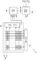
액정 패널(300)은 영상이 표시되는 표시부(DA)와 영상이 표시되지 않는 비표 시부(PA)로 구분된다.The
표시부(DA)는 다수의 게이트 라인(G1~Gn), 다수의 데이터 라인(D1~Dm), 스위칭 소자(미도시) 및 화소 전극(미도시)이 형성된 제1 기판(미도시)과, 컬러 필터(미도시)와 공통 전극(미도시)이 형성된 제2 기판(미도시), 제1 기판(미도시)과 제2 기판(미도시) 사이에 개재된 액정층(미도시)을 포함하여 영상을 표시한다. 게이트 라인(G1~Gn)은 대략 행 방향으로 연장되어 서로가 거의 평행하고, 데이터 라인(D1~Dm)은 대략 열 방향으로 연장되어 서로가 거의 평행하다.The display unit DA includes a first substrate (not shown) on which a plurality of gate lines G1 to Gn, a plurality of data lines D1 to Dm, a switching element (not shown), and a pixel electrode (not shown) are formed, and a color; Including a second substrate (not shown) having a filter (not shown) and a common electrode (not shown), and a liquid crystal layer (not shown) interposed between the first substrate (not shown) and the second substrate (not shown) Display the video. The gate lines G1 to Gn extend substantially in the row direction and are substantially parallel to each other, and the data lines D1 to Dm extend substantially in the column direction and are substantially parallel to each other.
도 2를 참조하여 도 1의 한 화소에 대해 설명하면, 제1 기판(100)의 화소 전극(PE)과 대향하도록 제2 기판(200)의 공통 전극(CE)의 일부 영역에 색필터(CF)가 형성될 수 있다. 예를 들어, i번째(i=1~n) 게이트 라인(Gi)과 j번째(j=1~m) 데이터 라인(Dj)에 연결된 화소(PX)는 신호선(Gi, Dj)에 연결된 스위칭 소자(Q)와 이에 연결된 액정 커패시터(liquid crystal capacitor, Clc) 및 유지 커패시터(storage capacitor, Cst)를 포함한다. 유지 커패시터(Cst)는 필요에 따라 생략될 수 있다. 스위칭 소자(Q)는 a-Si(amorphous - silicon)으로 이루어진 TFT이다.1, a color filter CF (CF) is formed in a part of the common electrode CE of the
비표시부(PA)는 제1 기판(도 2의 100 참조)이 제2 기판(도 2의 200 참조)보다 더 넓게 형성되어 영상이 표시되지 않는 부분을 의미한다.The non-display portion PA refers to a portion where the first substrate (see 100 in FIG. 2) is formed wider than the second substrate (see 200 in FIG. 2) and the image is not displayed.
데이터 구동부(700)는, 예컨데 타이밍 컨트롤러(500)로부터 영상 신호(DAT), 데이터 제어 신호(CONT)를 제공받아, 영상 신호(DAT)에 대응하는 영상 데이터 전압을 각 데이터 라인(D1~Dm)에 제공한다. 여기서 데이터 제어 신호(CONT)는 데이터 구동부(700)의 동작을 제어하는 신호로써, 데이터 구동부(700)의 동작을 개시하는 수평 개시 신호, 두 개의 데이터 전압의 출력을 지시하는 로드 신호 등을 포함한다.For example, the
게이트 구동부(400)는 제1 클럭 신호(CKV) 및 제2 클럭 신호(CKVB), 제2 스캔 개시 신호(STVP) 및 게이트 오프 전압(Voff)을 제공받아 다수의 게이트 라인(G1~Gn)에 게이트 신호를 제공한다.The
여기서 도 3 및 도 4에 도시된 회로를 일예로, 게이트 구동부(400)에 대하여 구체적으로 설명한다. 다만, 게이트 구동부(400)는, 적어도 하나의 a-Si TFT를 포함하고, 도 3 및 도 4에 도시된 바에 한정되는 것은 아니다.3 and 4, the
게이트 구동부(400)는 다수의 스테이지(ST1,…, STn+1)를 포함하는데, 각 스테이지(ST1,…, STn+1)는 서로 종속적으로 연결되어 있으며, 순차적으로 게이트 신호(Gout1,…, Gout(n+1))를 출력하며, 게이트 오프 전압(Voff), 제1 클럭 신호(CKV) 및 제2 클럭 신호(CKVB), 초기화 신호(INT)가 입력된다. 마지막 스테이지(STn+1)를 제외한 모든 스테이지는 액정 패널(미도시)의 게이트 라인(미도시)과 일대일로 연결되어 있다. 여기서 제1 클럭 신호(CKV) 및 제2 클럭 신호(CKVB)는, 상술한 바와 같이 프레임 주파수에 관계없이 게이트 구동부(400)의 오동작을 최소화할 수 있는 소정의 듀티비를 갖는 신호이다.The
각 스테이지(ST1,…, STn+1)는 제1 클럭 단자(CK1), 제2 클럭 단자(CK2), 셋 단자(S), 리셋 단자(R), 전원 전압 단자(GV), 프레임 리셋 단자(FR), 게이트 출력 단자(OUT1) 및 캐리 출력 단자(OUT2)를 가지고 있다.Each stage ST1 ,..., STn+1 has a first clock terminal CK1, a second clock terminal CK2, a set terminal S, a reset terminal R, a power supply voltage terminal GV, and a frame. It has the reset terminal FR, the gate output terminal OUT1, and the carry output terminal OUT2.
각 스테이지(ST1,…, STn+1), 예를 들면, j번째 스테이지(STj)의 셋 단자(S)에는 전단 스테이지(STj-1)의 캐리 신호(Cout(j-1))가, 리셋 단자(R)에는 후단 스테이지(STj+1)의 게이트 신호(Gout(j+1))가 입력되고, 제1 클럭 단자(CK1) 및 제2 클럭 단자(CK2)에는 제1 클럭 신호(CKV) 및 제2 클럭 신호(CKVB)가 입력되며, 전원 전압 단자(GV)에는 게이트 오프 전압(Voff)이 입력되며, 프레임 리셋 단자(FR)에는 초기화 신호(INT)가 입력된다. 게이트 출력 단자(OUT1)는 게이트 신호(Gout1)를 출력하고, 캐리 출력 단자(OUT2)는 캐리 신호(Cout(j))를 출력한다. 마지막 스테이지(STn+1)의 캐리 신호(Cout(n+1))는 초기화 신호로서 각 스테이지(ST1,…, STn+1)에 제공된다.The carry signal Cout(j-1) of the front stage STj-1 is provided to the set terminal S of each stage ST1 ,..., STn+1 , for example, the j th stage STj. Is input to the reset terminal R, and the gate signal Gout(j + 1 ) of the rear stage STj+1 is input to the first clock terminal CK1 and the second clock terminal CK2. The clock signal CKV and the second clock signal CKVB are input, the gate-off voltage Voff is input to the power supply voltage terminal GV, and the initialization signal INT is input to the frame reset terminal FR. The gate output terminal OUT1 outputs the gate signal Gout1 , and the carry output terminal OUT2 outputs the carry signal Cout(j) . A final stage carry signal(Cout (n + 1)) of the(n+1 ST) is provided as a reset signal to each stage(ST 1, ..., ST n +1).
단, 첫 번째 스테이지(ST1)에는 전단 캐리 신호 대신 제2 스캔 개시 신호(STVP)가 입력되며, 마지막 스테이지(STn+1)에는 후단 게이트 신호 대신 제2 스캔 개시 신호(STVP)가 입력된다.However, the second scan start signal STVP is input to the first stage ST1 instead of the front carry signal, and the second scan start signal STVP is input to the last stage STn+1 instead of the rear gate signal. .
여기서 도 4를 참조하여 도 9의 j번째 스테이지(STj)에 대하여 상세히 설명한다.Here, the j-th stage STj of FIG. 9 will be described in detail with reference to FIG. 4.
도 4를 참조하면, j번째 스테이지(STj)는 버퍼부(410), 충전부(420), 풀업부(430), 캐리 신호 발생부(470), 풀다운부(440), 방전부(450) 및 홀딩부(460)를 포함한다.Referring to FIG. 4, the j th stage STj includes a
버퍼부(410)는 트랜지스터(T4)의 드레인과 게이트가 공통되어 셋 단자(S)를 통해 입력된 전단 스테이지(STn-1)의 캐리 신호(Cout(j-1))를, 소스에 연결된 충전부(420), 캐리 신호 발생부(470), 방전부(450) 및 홀딩부(460)에 제공한다.The
충전부(420)는 일단이 트랜지스터(T4)의 소스와 방전부(750)에 연결되고, 타단이 게이트 출력 단자(OUT1)에 연결된 캐패시터(C1)로 이루어진다. 충전부(420)는 전단 스테이지(STn-1)의 캐리 신호(Cout(j-1))에 따라 전하가 충전된다.One end of the charging
전단 스테이지(STn-1)의 캐리 신호(Cout(j-1))의 듀티비는 제1 클럭 신호(CKV) 및 제2 클럭 신호(CKVB)의 듀티비에 따라 달라진다. 즉, 제1 클럭 신호(CKV) 및 제2 클럭 신호(CKVB)의 듀티비가 증가하면, 스테이지(STn-1)의 캐리 신호(Cout(j-1))의 듀티비도 증가하고, 제1 클럭 신호(CKV) 및 제2 클럭 신호(CKVB)의 듀티비가 감소하면, 스테이지(STn-1)의 캐리 신호(Cout(j-1))의 듀티비도 감소한다.The duty ratio of the carry signal Cout(j-1 ) of the front stage STn-1 depends on the duty ratio of the first clock signal CKV and the second clock signal CKVB. That is, when the duty ratio of the first clock signal CKV and the second clock signal CKVB increases, the duty ratio of the carry signal Cout(j-1) of the stage STn-1 also increases, and the first clock When the duty ratios of the signal CKV and the second clock signal CKVB decrease, the duty ratio of the carry signal Cout(j-1) of the stage STn-1 also decreases.
일반적으로, 액정 표시 장치의 프레임 주파수가 저주파수인 경우, 제1 클럭 신호(CKV) 및 제2 클럭 신호(CKVB)는, 한 주기당 하이 레벨인 시간이 길게 된다. 제1 클럭 신호(CKV) 및 제2 클럭 신호(CKVB)의 한 주기당 하이 레벨인 시간이 긴 경우, 전단 스테이지(STn-1)의 캐리 신호(Cout(j-1))의 한 주기당 하이 레벨인 시간이 길게 되어 충전부(420)에 많은 전하량이 충전된다. 프레임 주파수가 고주파수인 경우에는 한 주기당 하이 레벨인 시간이 저주파수인 경우에 비해 작으므로, 충전부(420)에 적은 전하량이 충전된다.In general, when the frame frequency of the liquid crystal display device is a low frequency, the first clock signal CKV and the second clock signal CKVB have a high level of time per cycle. When the time, which is a high level per period of the first clock signal CKV and the second clock signal CKVB, is long, the period of the carry signal Cout(j-1 ) of the front stage STn-1 is long. As the time at a high level becomes long, a large amount of charge is charged in the
여기서 충전부(430)의 전하량은 풀업부(430)의 턴온 및 턴오프를 결정한다. 즉, 프레임 주파수가 저주파수인 경우에는 충전부(430)에 충전된 전하량이 많게되어 풀업부(430)가 쉽게 턴온 되고, 프레임 주파수가 고주파수인 경우에는 충전부(430)에 충전된 전하량이 적어 풀업부(430)가 쉽게 턴온되지 않을 수 있다. 그러나 본 발명에서는 프레임 주파수에 관계없이, 한 주기당 하이 레벨인 시간이 일정한 제1 클럭 신호(CKV) 및 제2 클럭 신호(CKVB)를 게이트 구동부(400)에 제공한다. 따라서, 충전부(420)에 충전되는 전하량은 일정하게 유지된다.Herein, the charge amount of the charging
풀업부(430)는 드레인이 제1 클럭 단자(CK1)에 연결되고, 게이트가 캐패시터(C1)의 일단에 연결되며, 소스가 캐패시터(C1)의 타단 및 게이트 출력 단자(OUT1)에 연결된 트랜지스터(T1)를 포함한다. 충전부(420)의 커패시터(C1)가 충전되면, 트랜지스터(T1)는 턴온되고, 제1 클럭 단자(CK1)를 통해 입력되는 제1 클럭 신호(CKV)를 게이트 출력 단자(OUT1)를 통해 게이트 신호(Gout(j))로 제공한다.The pull-up
상술한 바와 같이, 프레임 주파수가 저주파수이면, 제1 클럭 신호(CKV) 및 제2 클럭 신호(CKVB)의 한 주기당 하이 레벨인 시간이 길기 때문에, 클럭 신호 풀업부(430)는 쉽게 턴온된다. 특히 고온에서 전하 이동도가 높아지므로, 풀업부(430)는 노이즈에 의해 쉽게 턴온될 수 있고, 이러한 경우, 한 프레임동안 여러 번 게이트 온 전압을 게이트 신호(Gout(j))로서 게이트 라인에 출력할 수 있다. 그러나 본 발명에서는, 프레임 주파수에 관계없이, 제1 클럭 신호(CKV) 및 제2 클럭 신호(CKVB)의 한 주기당 하이 레벨인 시간이 일정하므로, 충전부(440)에 소정의 전하량이 충전되어, 저주파수에서도 풀업부(430)의 오동작을 방지할 수 있다. 여기서 풀업부(430)의 오동작을 최소화하는 제1 클럭 신호(CKV) 및 제2 클럭 신호(CKVB)의 한 주기당 하이 레벨인 시간은 실험적으로 도출될 수 있다.As described above, when the frame frequency is a low frequency, the clock signal pull-up
여기서 한 주기당 하이 레벨인 시간이 일정한 제1 클럭 신호(CKV) 및 제2 클럭 신호(CKVB)는, 타이밍 컨트롤러(500) 및 클럭 생성부(600)가 제공하는데, 이에 대한 설명은 후술한다.Here, the
한편, 캐리 신호 발생부(470)는 드레인이 제1 클럭 단자(CK1)에 연결되고, 소스가 게이트 출력 단자(OUT1)에 연결되고, 게이트가 버퍼부(710)와 연결되어 있는 트랜지스터(T15)와 게이트와 소스에 연결된 커패시터(C2)를 포함한다. 커패시터(C2)는 충전부(420)와 동일하게 충전되고, 트랜지스터는 커패시터(C2)가 충전되면, 제1 클럭 신호(CKV)를 캐리 출력 단자(OUT2)를 통해 캐리 신호(Cout(j))로 출력한다.The
풀다운부(440)는 드레인이 트랜지스터(T1)의 소스 및 캐패시터(C1)의 타단에 연결되고, 소스가 전원 전압 단자(GV)에 연결되고, 게이트가 리셋 단자(R)에 연결된 트랜지스터(T2)를 포함한다. 풀다운부(440)는 리셋 단자(R)를 통해 입력된 다음 스테이지(STj+1)의 게이트 신호(Gout(j+1))에 턴온되어 게이트 신호(Gout(j))를 게이트 오프 전압(Voff)으로 풀다운시킨다.Down
방전부(450)는, 게이트가 리셋 단자(R)에 연결되고 드레인이 캐패시터(C1)의 일단에 연결되고 소스가 전원 전압 단자(GV)에 연결되어, 다음 스테이지(STj+1)의 게이트 신호(Gout(j+1))에 응답하여 충전부(420)를 방전시키는 트랜지시터(T9)와, 게 이트가 프레임 리셋 단자(FR)에 연결되고 드레인이 캐패시터(C1)의 일단에 연결되고 소스가 전원 전압 단자(GV)에 연결되어, 충전부(420)를 방전시키는 트랜지시터(T6)를 포함한다. 즉, 방전부(450)는 다음 스테이지(STj+1)의 게이트 신호(Gout(j+1)) 또는 초기화 신호(INT)에 응답하여 캐패시터(C1)에 충전된 전하를 소스를 통해 게이트 오프 전압(Voff)으로 방전한다.The
홀딩부(460)는 게이트 신호(Gout(j))가 하이 레벨일 때 트랜지스터(T3)가 오프 상태를 유지하여 홀드 동작을 수행하고, 게이트 신호(Gout(j))가 하이 레벨에서 로우 레벨로 변환된 후에는 트랜지스터(T3, T5)가 턴온되어 홀드 동작을 수행한다.The holding
좀더 구체적으로 설명하면, 트랜지스터(T3)는 드레인이 게이트 출력 단자(OUT1)에 연결되고, 소스가 게이트 오프 전압(Voff)에 연결된다. 트랜지스터(T7, T8)는 게이트 출력 단자(OUT1)를 통해 출력되는 게이트 신호(Gout(j))가 하이 레벨일 때 턴온되어 트랜지스터(T3)의 게이트를 게이트 오프 전압(Voff)으로 풀다운시켜 턴 오프시키고, 따라서 게이트 신호(Gout(j))의 하이 레벨을 홀딩한다.More specifically, the drain of the transistor T3 is connected to the gate output terminal OUT1, and the source is connected to the gate-off voltage Voff. The transistors T7 and T8 are turned on when the gate signal Gout(j) output through the gate output terminal OUT1 is at the high level to pull down the gate of the transistor T3 to the gate off voltage Voff, And thus holds the high level of the gate signal Gout(j) .
트랜지스터(T11)는 드레인이 셋 단자(S)에 연결되고, 게이트가 제2 클럭 단자(CK2)에 연결되며, 소스가 캐패시터(C1)의 일단에 연결된다. 트랜지스터(T10)는 드레인이 트랜지스터(T11)의 소스 및 캐패시터(C1)의 일단에 연결되고, 게이트가 제1 클럭 단자(CK1)에 연결되며, 소스가 게이트 출력 단자(OUT1)에 연결된다. 트랜지스터(T5)는 드레인이 게이트 출력 단자(OUT1)에 연결되고, 게이트가 트랜지스 터(T11)의 게이트와 공통하여 제2 클럭 단자(CK2)에 연결되며, 소스가 전원 전압 단자(GV)에 연결된다.The transistor T11 has a drain connected to the set terminal S, a gate connected to the second clock terminal CK2, and a source connected to one end of the capacitor C1. The transistor T10 has a drain connected to the source of the transistor T11 and one end of the capacitor C1, a gate connected to the first clock terminal CK1, and a source connected to the gate output terminal OUT1. The transistor T5 has a drain connected to the gate output terminal OUT1, a gate connected to the second clock terminal CK2 in common with the gate of the transistor T11, and a source connected to the power supply voltage terminal GV. Connected.
제2 클럭 신호(CKVB)가 하이 레벨일 때 게이트 신호(Gout(j))는 로우 레벨이고 트랜지스터(T5)는 턴온되어, 게이트 출력 단자(OUT1)를 게이트 오프 전압(Voff)으로 홀딩하는 동작을 수행한다.When the second clock signal CKVB is at the high level, the gate signal Gout(j) is at the low level and the transistor T5 is turned on to hold the gate output terminal OUT1 at the gate off voltage Voff .
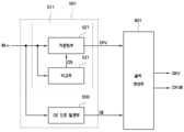
한편, 도 1의 타이밍 컨트롤러(500)는 외부의 그래픽 제어기(미도시)로부터 입력 영상 신호(R, G, B) 및 이의 표시를 제어하는 입력 제어 신호를 수신한다. 입력 제어 신호의 예로는 수직 동기 신호(Vsinc)와 수직 동기 신호(Hsync), 메인 클럭 신호(Mclk), 데이터 인에이블 신호(DE) 등이 있다. 여기서 메인 클럭 신호(Mclk)의 주파수는 프레임 주파수에 따라 결정된다.Meanwhile, the
타이밍 컨트롤러(500)는 입력 영상 신호(R, G, B)와 입력 제어 신호를 기초로 데이터 제어 신호(CONT2)를 생성하여, 데이터 제어 신호(CONT2)와 영상 데이터(DAT)를 데이터 구동부(700)로 보낸다.The
또한, 타이밍 컨트롤러(500)는 제1 클럭생성 제어신호(OE), 제2 클럭생성 제어신호(CPV) 및 제1 스캔 개시 신호(STV)를 클럭 생성부(600)에 제공한다. 여기서 제1 클럭생성 제어신호(OE)는 게이트 신호를 인에이블시키는 게이트 인에이블 신호이고, 제1 스캔 개시 신호(STV)는 한 프레임의 시작을 알리는 신호이고, 제2 클럭생성 제어신호(CPV)는 게이트 신호의 듀티비를 결정하는 게이트 클럭 신호로서, 듀티비가 가변되는 신호이다.In addition, the
일반적으로, 프레임 주파수가 결정되면, 제2 클럭생성 제어신호(CPV)의 주파수 및 듀티비가 결정된다. 즉, 프레임 주파수에 따라, 제2 클럭생성 제어신호(CPV)의 한 주기당 하이 레벨인 시간이 결정된다. 그러나, 본 발명에서는, 프레임 주파수에 관계없이, 한 주기당 하이 레벨인 시간을 일정하게 한다. 상술한 바와 같이, 제1 클럭 신호(CKV) 및 제2 클럭 신호(CKVB)가 한 주기당 하이 레벨인 시간이 일정해야 게이트 구동부(400)의 오동작을 방지할 수 있는데, 제1 클럭 신호(CKV) 및 제2 클럭 신호(CKVB)는, 제1 클럭생성 제어신호(OE) 및 제2 클럭생성 제어신호(CPV)에 의해 생성되므로, 타이밍 컨트롤러(500)는 프레임 주파수에 관계없이, 한 주기당 하이 레벨인 시간이 일정한 제2 클럭생성 제어신호(CPV)를 출력한다. 즉, 타이밍 컨트롤러(500)는 제2 클럭생성 제어신호(CPV)의 주파수는 변화시키지 않고, 듀티비를 조절한다.In general, when the frame frequency is determined, the frequency and duty ratio of the second clock generation control signal CPV are determined. That is, according to the frame frequency, a time having a high level per period of the second clock generation control signal CPV is determined. However, in the present invention, the time at a high level per cycle is made constant regardless of the frame frequency. As described above, malfunction of the
클럭 생성부(600)는 제1 클럭생성 제어신호(OE), 제2 클럭생성 제어신호(CPV) 및 제1 스캔 개시 신호(STV)를 제공받아, 제1 클럭 신호(CKV), 제2 클럭 신호(CKVB), 제2 스캔 개시 신호(STVP) 및 게이트 오프 전압(Voff)을 게이트 구동부(400)에 제공한다.The
여기서, 제1 클럭 신호(CKV) 및 제2 클럭 신호(CKVB)의 듀티비는 제2 클럭생성 제어신호(CPV)의 듀티비에 따라 가변된다. 예컨데 제2 클럭생성 제어신호(CPV)의 듀티비가 증가하면, 제1 클럭 신호(CKV) 및 제2 클럭 신호(CKVB)의 듀티비도 증가하고, 제2 클럭생성 제어신호(CPV)의 듀티비가 감소하면, 제1 클럭 신호(CKV) 및 제2 클럭 신호(CKVB)의 듀티비도 감소할 수 있다. 즉, 타이밍 컨트롤러(500)가 프 레임 주파수에 관계없이, 한 주기당 하이 레벨인 시간이 일정한 제2 클럭생성 제어신호(CPV)을 제공하므로, 클럭 생성부(600)는, 한 주기당 하이 레벨인 시간이 일정한 제1 클럭 신호(CKV) 및 제2 클럭 신호(CKVB)를 생성한다.Here, the duty ratio of the first clock signal CKV and the second clock signal CKVB is varied according to the duty ratio of the second clock generation control signal CPV. For example, when the duty ratio of the second clock generation control signal CPV increases, the duty ratio of the first clock signal CKV and the second clock signal CKVB also increases, and the duty ratio of the second clock generation control signal CPV decreases. If so, the duty ratio of the first clock signal CKV and the second clock signal CKVB may also be reduced. That is, since the
다시 말해서, 타이밍 컨트롤러(500)가 현재 액정 표시 장치(10)가 동작하고 있는 프레임 주파수에 관계없이, 게이트 구동부(400)의 오동작이 최소가 되도록 제2 클럭생성 제어신호(CPV)의 듀티비를 조절하고, 클럭 생성부(600)는 제2 클럭생성 제어신호(CPV)에 따라 제1 클럭 신호(CKV) 및 제2 클럭 신호(CKVB)를 제공한다. 따라서, 현재 액정 표시 장치(10)가 구동하고 있는 프레임 주파수에 관계없이, 게이트 구동부(400)의 오동작을 방지할 수 있다.In other words, the
이하에서 구체적인 실시예들을 통해 타이밍 컨트롤러(500) 및 클럭 생성부(600)에 대해 설명한다.Hereinafter, the
도 5 내지 도 9를 참조하여 본 발명의 일 실시예에 따른 액정 표시 장치를 설명한다. 도 5는 본 발명의 일 실시예에 따른 액정 표시 장치의 타이밍 컨트롤러를 설명하기 위한 블록도이고, 도 6은 본 발명의 일 실시예에 따른 액정 표시 장치의 클럭 생성부를 설명하기 위한 블록도이고, 도 7은 도 6의 디플립플롭을 설명하기 위한 블록도이고, 도 8 및 도 9는 도 5 및 도 6의 타이밍 컨트롤러 및 클럭 생성부를 설명하기 위한 신호도이다. 설명의 편의상 제2 스캔 개시 신호 및 게이트 오프 전압의 출력 과정은 생략한다.A liquid crystal display according to an exemplary embodiment of the present invention will be described with reference to FIGS. 5 to 9. FIG. 5 is a block diagram illustrating a timing controller of a liquid crystal display according to an exemplary embodiment of the present invention. FIG. 6 is a block diagram illustrating a clock generator of a liquid crystal display according to an exemplary embodiment. FIG. 7 is a block diagram illustrating the def flip-flop of FIG. 6, and FIGS. 8 and 9 are signal diagrams illustrating the timing controller and the clock generator of FIGS. 5 and 6. For convenience of description, an output process of the second scan start signal and the gate off voltage is omitted.
일반적으로 액정 표시 장치의 프레임 주파수가 결정되면, 메인 클럭 신호(Mclk), 제2 클럭생성 제어신호(CPV)의 주파수 및 듀티비, 제1 클럭 신호(CKV) 및 제2 클럭 신호(CKVB)의 듀티비가 결정된다. 예컨데, 프레임 주파수에 따라, 메인 클럭 신호(Mclk)의 주파수가 결정되면, 제2 클럭생성 제어신호(CPV)는 메인 클럭 신호(Mclk)의 라이징 에지의 카운팅하는 횟수에 따라 한 주기당 하이 레벨인 시간과 로우 레벨인 시간이 결정된다. 여기서 도 8 및 도 9를 참조하여 설명하면, 일반적인 타이밍 컨트롤러의 경우, 메인 클럭 신호(Mclk)의 라이징 에지를 J1번 카운팅하는 동안 하이 레벨이고, K1번 카운팅 하는 동안 로우 레벨을 출력하도록 카운팅 횟수가 기 설정되어 있다.(이하에서 기 설정된 카운팅 횟수를 '기준 카운팅 횟수'라 함). 따라서 비교용 제2 클럭생성 제어신호(CPV_REF)의 하이 레벨인 시간은, 메인 클럭 신호(Mclk)의 주파수 및 기준 카운팅 횟수에 따라 결정된다.In general, when the frame frequency of the liquid crystal display is determined, the frequency and duty ratio of the main clock signal Mclk, the second clock generation control signal CPV, the first clock signal CKV and the second clock signal CKVB are determined. Duty ratio is determined. For example, when the frequency of the main clock signal Mclk is determined according to the frame frequency, the second clock generation control signal CPV has a high level per cycle according to the number of counting of the rising edge of the main clock signal Mclk. The time and the low level time are determined. Referring to FIGS. 8 and 9, in the case of a general timing controller, the rising edge of the main clock signal Mclk is at a high level while counting J1 and outputs a low level while counting K1. The number of times is set in advance (hereinafter, the preset counting number is referred to as 'reference counting number'). Therefore, the time which is the high level of the comparison second clock generation control signal CPV_REF is determined according to the frequency of the main clock signal Mclk and the reference counting count.
제2 클럭생성 제어신호(CPV)의 한 주기당 하이 레벨인 시간을 게이트 구동부(도 1의 400 참조)의 오동작을 최소화하는 소정의 시간으로 조절하기 위해, 메인 클럭 신호(Mclk)의 주파수를 측정하고, 그에 따라 메인 클럭 신호(Mclk)의 라이징 에지 또는 폴링 에지의 카운팅 횟수를 조절해야 한다. 즉, 실험을 통해 게이트 구동부(도 1의 400 참조)의 오동작을 최소화하는 메인 클럭 신호의 주파수(이하 '제1 기준 주파수'라 함)를 찾을 수 있으므로, 입력되는 메인 클럭 신호(Mclk)의 주파수를 측정하고, 메인 클럭 신호(Mclk)의 주파수가 제1 기준 주파수보다 작은 경우에는 카운팅 횟수를 감소시켜 제2 클럭생성 제어신호(CPV)의 한 주기당 하이 레벨인 시간을 감소시킨다. 또는, 입력되는 메인 클럭 신호(Mclk)의 주파수가 제1 기준 주파수보다 큰 경우에는 카운팅 횟수를 증가시켜 제2 클럭생성 제어신호(CPV)의 한 주기당 하이 레벨인 시간을 증가시킨다.The frequency of the main clock signal Mclk is measured to adjust the time, which is a high level per cycle of the second clock generation control signal CPV, to a predetermined time to minimize the malfunction of the gate driver (see 400 of FIG. 1). The number of counts of the rising edge or the falling edge of the main clock signal Mclk must be adjusted accordingly. That is, the experiment can find the frequency of the main clock signal (hereinafter referred to as 'first reference frequency') that minimizes the malfunction of the gate driver (refer to 400 of FIG. 1), and thus the frequency of the input main clock signal Mclk. When the frequency of the main clock signal Mclk is smaller than the first reference frequency, the counting number is decreased to decrease the time at which the high level is generated per cycle of the second clock generation control signal CPV. Alternatively, when the frequency of the input main clock signal Mclk is greater than the first reference frequency, the counting number is increased to increase the time which is a high level per one period of the second clock generation control signal CPV.
먼저, 도 5 및 도 8을 참조하여, 메인 클럭 신호(Mclk)의 주파수가 제1 기준 주파수보다 작은 경우, 제2 클럭생성 제어신호(CPV)를 출력하는 과정을 설명한다.First, a process of outputting the second clock generation control signal CPV when the frequency of the main clock signal Mclk is smaller than the first reference frequency will be described with reference to FIGS. 5 and 8.
타이밍 컨트롤러(500)는 제1 클럭생성 제어신호 발생부(550)와 제2 클럭생성 제어신호 발생부(511)를 포함한다.The
메인 클럭 신호(Mclk)가 제공되면, 제1 클럭생성 제어신호 발생부(550)는 메인 클럭 신호(Mclk)에 따라 제1 클럭생성 제어신호(OE)를 출력한다. 예컨데, 메인 클럭 신호(Mclk)의 라이징 에지 또는 폴링 에지를 카운팅하여 하이 레벨 또는 로우 레벨인 구간이 결정될 수 있다.When the main clock signal Mclk is provided, the first clock generation
비교부(531)는 메인 클럭 신호(Mclk)를 제공받아 제1 기준 주파수와 주파수 크기를 비교하여, 카운팅 제어 신호(CN)를 카운팅부(521)에 제공한다. 메인 클럭 신호(Mclk)의 주파수가 제1 기준 주파수보다 작은 경우에는, 비교부(531)는 기준 카운팅 횟수(J1)보다 작은 J2번의 카운팅 횟수에 해당하는 카운팅 제어 신호(CN)를 카운팅부(521)에 제공한다.The
카운팅(521)부는, 기 설정된 기준 카운팅 횟수(J1, K1)로 메인 클럭 신호(Mclk)를 카운팅하여 비교용 제2 클럭생성 제어신호(CPV_REF)를 출력하다가, 비교부(531)로부터 카운팅 제어 신호(CN)를 제공받은 후, 메인 클럭 신호(Mclk)의 라이징 에지를 J2번 카운팅하는 동안 하이 레벨이고, K1번보다 큰 K2번 카운팅하는 동안 로우 레벨인 제2 클럭생성 제어신호(CPV)를 출력한다.The
즉, 제2 클럭생성 제어신호 발생부(511)는, 메인 클럭 신호(Mclk)의 주파수가 제1 기준 주파수보다 작은 경우, 듀티비가 감소된 제2 클럭생성 제어신호(CPV)를 출력한다.That is, when the frequency of the main clock signal Mclk is smaller than the first reference frequency, the second clock generation
도 5 및 도 8을 참조하여 메인 클럭 신호(Mclk)의 주파수가 제1 기준 주파수보다 큰 경우, 듀티비가 증가된 제2 클럭생성 제어신호(CPV)를 출력하는 과정을 설명한다.5 and 8, a process of outputting the second clock generation control signal CPV having increased duty ratio when the frequency of the main clock signal Mclk is greater than the first reference frequency will be described.
메인 클럭 신호(Mclk)의 주파수가 제1 기준 주파수보다 큰 경우, 비교부(531)는 기준 카운팅 횟수(J1)보다 큰 J3번의 카운팅 횟수에 해당하는 카운팅 제어 신호(CN)를 카운팅부(521)에 제공한다.When the frequency of the main clock signal Mclk is greater than the first reference frequency, the
카운팅(521)부는, 기 설정된 기준 카운팅 횟수(J1, K1)로 메인 클럭 신호(Mclk)를 카운팅하여 비교용 제2 클럭생성 제어신호(CPV_REF)를 출력하다가, 비교부(531)로부터 카운팅 제어 신호(CN)를 제공받은 후, 메인 클럭 신호(Mclk)의 라이징 에지를 J3번 카운팅하는 동안 하이 레벨이고, K3번 카운팅하는 동안 로우 레벨인 제2 클럭생성 제어신호(CPV)를 출력한다.The
즉, 제2 클럭생성 제어신호 발생부(511)는, 메인 클럭 신호(Mclk)의 주파수가 제1 기준 주파수보다 큰 경우, 비교용 제2 클럭생성 제어신호(CPV_REF)의 듀티비보다 커진 제2 클럭생성 제어신호(CPV)를 출력한다.That is, when the frequency of the main clock signal Mclk is greater than the first reference frequency, the second clock generation
여기서, 비교부(531)는, 기 저장된 제1 기준 주파수와 메인 클럭 신호(Mclk)의 주파수를 비교하는데, 입력되는 메인 클럭 신호(Mclk)의 주파수는 단위 시간당 메인 클럭 신호(Mclk)의 라이징 에지 또는 폴링 에지를 카운트하여 메인 클럭 신호(Mclk)의 주파수를 판단할 수 있다.Here, the
다시 말하면, 타이밍 컨트롤러(500)는, 프레임 주파수에 관계없이, 한 주기당 하이 레벨인 시간이 일정한 제2 클럭생성 제어신호(CPV)를 출력한다. 따라서, 타이밍 컨트롤러(5601)는 게이트 구동부(도 1의 400)의 오동작을 최소화할 수 있는 제2 클럭생성 제어신호(CPV)를 클럭 생성부(601)에 제공한다.In other words, the
다음으로 도 6 내지 도 9를 참조하여, 듀티비가 조절된 제2 클럭생성 제어신호(CPV)를 이용하여, 제1 클럭 신호(CKV) 및 제2 클럭 신호(CKVB)를 생성하는 클럭 생성부(601)에 대해 설명한다.Next, referring to FIGS. 6 to 9, a clock generator configured to generate the first clock signal CKV and the second clock signal CKVB using the second clock generation control signal CPV having the duty ratio adjusted ( 601) will be described.
먼저, 도 6 내지 도 8을 참조하여, 메인 클럭 신호(Mclk)가 제1 기준 주파수보다 작은 경우, 제1 클럭 신호(CKV) 및 제2 클럭 신호(CKVB)를 생성하는 과정에 대해 설명한다.6 to 8, a process of generating the first clock signal CKV and the second clock signal CKVB when the main clock signal Mclk is smaller than the first reference frequency will be described.
클럭 생성부(601)는 논리합 연산자(OR), 디플립플롭(610), 제1 클럭 전압 인가부(620), 제2 클럭 전압 인가부(630) 및 전하 공유부(640)을 포함한다. 다만, 클럭 생성부(601)의 내부 회로가 이에 한정되는 것은 아니다.The
논리합 연산자(OR)는 제1 클럭생성 제어신호(OE)와 제2 클럭생성 제어신호(CPV)를 입력받아 논리합 연산을 하여 제3 클럭생성 제어신호(CPVX)를 생성하고, 디플립플롭(610)에 제공한다.The OR operator receives the first clock generation control signal OE and the second clock generation control signal CPV and performs an OR operation to generate a third clock generation control signal CPVX, and then deflip-
디플립플롭(610)은 도 7에 도시된 바와 같이, 제3 클럭생성 제어신호(CPVX)를 클럭 단자(CLK)로 입력받고, 입력 단자(D)와 출력바 단자(/Q)가 연결되어 있으 므로, 출력 단자(Q)에서는 제3 클럭생성 제어신호(CPVX)의 라이징 에지마다 토글(toggle)되는 제2 클럭 인에이블 신호(ECS)가 출력되고, 출력바 단자(/Q)에서는 제2 클럭 인에이블 신호(ECS)와 위상이 반대인 제1 클럭 인에이블 신호(OCS)가 출력된다(도 8 참조).As shown in FIG. 7, the flip-
제1 클럭 인에이블 신호(OCS)는 제1 클럭 전압 인가부(620)에 제공되고, 제2 클럭 인에이블 신호(ECS)는 제2 클럭 전압 인가부(630)에 제공된다.The first clock enable signal OCS is provided to the first clock
제1 클럭 전압 인가부(620)는 제1 클럭 인에이블 신호(OCS)에 인이에블되어, 제1 클럭 인에이블 신호(OCS)가 하이 레벨인 경우 하이 레벨(Von)이고(도 8의 제1 구간 참조), 제1 클럭 인에이블 신호(OCS)가 로우 레벨인 경우 로우 레벨(Voff)인 제1 클럭 신호(CKV)를 출력한다(도 8의 제2 구간 참조). 또한 제 2 클럭 전압 인가부는 제2 클럭 인에이블 신호(ECS)에 인이에블되어, 제2 클럭 인에이블 신호(ECS)가 하이 레벨인 경우 하이 레벨(Von)이고(도 8의 제1 구간 참조), 제2 클럭 인에이블 신호(ECS)가 로우 레벨인 경우 로우 레벨(Voff)인 제2 클럭 신호(CKVB)를 출력한다(도 8의 제2 구간 참조).The first clock
여기서, 전하 공유부(640)는 제3 클럭생성 제어신호(CPVX)를 입력받아, 제1 클럭 신호(CKV)와 제2 클럭 신호(CKVB)의 충전 및 방전시 전하를 공유시킨다.Here, the
좀더 구체적으로 설명하면, 도 8에 도시된 바와 같이, 제1 구간에서, 제1 클럭 신호(CKV)는 하이 레벨(Von)이고, 제2 클럭 신호(CKVB)는 로우 레벨(Voff)이다. 여기서 제3 클럭생성 제어신호(CPVX)가 로우 레벨이 되면, 제1 클럭 신호(CKV)는 방전을 시작하고, 제2 클럭 신호(CKVB)는 충전을 시작한다. 즉, 제3 구간에서, 전 하를 공유하면서, 제1 클럭 신호(CKV)는 방전되어 점차 로우 레벨(Voff)로 천이되고, 제2 클럭 신호(CKVB)는 제1 클럭 신호(CKV)로부터 제공된 전하가 충전되어 점차 하이 레벨(Von)로 천이된다.More specifically, as shown in FIG. 8, in the first period, the first clock signal CKV is at the high level Von and the second clock signal CKVB is at the low level Voff. Here, when the third clock generation control signal CPVX becomes low, the first clock signal CKV starts discharging, and the second clock signal CKVB starts charging. That is, in the third section, the first clock signal CKV is discharged and gradually transitions to the low level Voff while sharing charge, and the second clock signal CKVB is provided from the first clock signal CKV. The charge is charged and gradually transitions to the high level (Von).
제2 구간에서 제1 클럭 신호(CKV)는 로우 레벨(Voff)이 되고, 제2 클럭 신호(CKVB)는 하이 레벨(Von)이 된다. 다음으로 제3 구간에서는, 또 다시 전하를 공유하여 제1 클럭 신호(CKV)는 충전을 시작하고, 제2 클럭 신호(CKVB)는 방전을 시작한다. 여기서 전하를 공유하는 구간 즉, 제3 구간은 제3 클럭생성 제어신호(CPVX)의 듀티비에 따라 조절된다. 제3 클럭생성 제어신호(CPVX)의 듀티비가 증가하면, 제3 구간이 줄어든다. 또는 제3 클럭생성 제어신호(CPVX)의 듀티비가 감소하면, 제3 구간이 증가하고, 제1 구간 및 제2 구간은 줄어들게 된다. 즉, 제3 클럭생성 제어신호(CPVX)의 듀티비가 제1 클럭 신호(CKV) 및 제2 클럭 신호(CKVB)의 듀티비를 결정한다.In the second period, the first clock signal CKV becomes the low level Voff and the second clock signal CKVB becomes the high level Von. Next, in the third section, the first clock signal CKV starts charging and the second clock signal CKVB starts discharging again by sharing charges. In this case, the charge sharing period, that is, the third period, is adjusted according to the duty ratio of the third clock generation control signal CPVX. When the duty ratio of the third clock generation control signal CPVX is increased, the third section is reduced. Alternatively, when the duty ratio of the third clock generation control signal CPVX decreases, the third section increases, and the first section and the second section decrease. That is, the duty ratio of the third clock generation control signal CPVX determines the duty ratio of the first clock signal CKV and the second clock signal CKVB.
도 9를 참조하면, 메인 클럭 신호(Mclk)의 주파수가 제1 기준 주파수보다 큰 경우, 상술한 바와 같이, 제2 클럭생성 제어신호(CPV)의 듀티비가 증가하고, 따라서 제3 클럭생성 제어신호(CPVX)의 듀티비도 증가하게 된다. 제3 클럭생성 제어신호(CPVX)의 로우 레벨인 구간이 줄어들게 되므로, 전하를 공유하는 구간인 제3 구간이 줄어들게 되고, 제1 구간 및 제2 구간이 증가하게 된다. 즉, 제1 클럭 신호(CKV) 및 제2 클럭 신호(CKVB)의 듀티비가 증가하게 된다.Referring to FIG. 9, when the frequency of the main clock signal Mclk is greater than the first reference frequency, as described above, the duty ratio of the second clock generation control signal CPV increases, and thus, the third clock generation control signal. The duty ratio of (CPVX) also increases. Since the section which is the low level of the third clock generation control signal CPVX is reduced, the third section which is the charge sharing section is reduced, and the first section and the second section are increased. That is, the duty ratio of the first clock signal CKV and the second clock signal CKVB increases.
따라서, 프레임 주파수에 관계없이, 제1 클럭 신호(CKV) 및 제2 클럭 신호(CKVB)의 듀티비가 가변되어, 한 주기당 하이 레벨인 시간이 일정하게 유지된다. 여기서 한 주기당 하이 레벨인 시간은 게이트 구동부(도 1의 400 참조)의 오동작을 최소화할 수 있는 시간이다.Therefore, regardless of the frame frequency, the duty ratios of the first clock signal CKV and the second clock signal CKVB are varied, so that the time at a high level per period is kept constant. Here, the high level of time per cycle is a time for minimizing malfunction of the gate driver (see 400 of FIG. 1).
이하에서 도 10을 참조하여 본 발명의 다른 실시예에 따른 액정 표시 장치를 설명한다. 도 10은 본 발명의 다른 실시예에 따른 액정 표시 장치의 타이밍 제어부를 설명하기 위한 블록도이다. 도 5에 도시된 구성 요소와 동일한 기능을 하는 구성 요소에 대해서는 동일한 도면 부호를 사용하고, 설명의 편의상 해당 구성 요소의 상세한 설명은 생략한다.Hereinafter, a liquid crystal display according to another exemplary embodiment of the present invention will be described with reference to FIG. 10. 10 is a block diagram illustrating a timing controller of a liquid crystal display according to another exemplary embodiment of the present invention. The same reference numerals are used for components that have the same function as the components shown in FIG. 5, and detailed descriptions of the corresponding components are omitted for convenience of description.
이전 실시예에서는 메인 클럭 신호(Mclk)를 제1 기준 주파수와 비교하여 제2 클럭생성 제어신호(CPV)의 듀티비를 조절한다. 본 실시예에서는, 이와 달리, 제2 클럭생성 제어신호(CPV)를 제2 기준 주파수와 비교하여 제2 클럭생성 제어신호(CPV)의 듀티비를 조절한다. 여기서 제2 기준 주파수는 게이트 구동부(도 1의 400 참조)의 오동작을 최소화하는 제2 클럭생성 제어신호(CPV)의 주파수를 의미한다.In the previous embodiment, the duty ratio of the second clock generation control signal CPV is adjusted by comparing the main clock signal Mclk with the first reference frequency. In the present embodiment, the duty ratio of the second clock generation control signal CPV is adjusted by comparing the second clock generation control signal CPV with the second reference frequency. Here, the second reference frequency refers to the frequency of the second clock generation control signal CPV which minimizes the malfunction of the gate driver (see 400 of FIG. 1).
도 10을 참조하여 좀 더 구체적으로 설명하면, 먼저 카운팅부(522)는 기준 카운팅 횟수에 대응하는 카운팅 제어 신호(CN)를 제공받아, 하이 레벨 및 로우 레벨을 출력한다.Referring to FIG. 10, the
다음으로, 비교부(532)가 제2 클럭생성 제어신호(CPV)를 입력받아, 제2 클럭생성 제어신호(CPV)의 주파수가 제2 기준 주파수보다 작으면, 기준 카운팅 횟수보다 더 작은 카운팅 횟수를 나타내는 카운팅 제어 신호(CN)를 제공하고, 제2 클럭생성 제어신호(CPV)의 주파수가 제2 기준 주파수보다 크면, 제2 기준 카운팅 횟수보 다 더 큰 카운팅 횟수를 나타내는 카운팅 제어 신호(CN)를 제공한다.Next, when the
카운팅부(522)는 비교부(531)로부터 제공된 카운팅 제어 신호(CN)에 따라 메인 클럭 신호(Mclk)의 라이징 에지 또는 폴링 에지를 카운팅하는 동안 하이 레벨인 제2 클럭생성 제어신호(CPV)를 출력한다. 카운팅부(521)는, 제2 클럭생성 제어신호(CPV)의 주파수가 제2 기준 주파수보다 작으면 제2 클럭생성 제어신호(CPV)의 듀티비를 감소시키고, 제2 클럭생성 제어신호(CPV)의 주파수가 제2 기준 주파수보다 크면 제2 클럭생성 제어신호(CPV)의 듀티비를 증가시킨다. 따라서, 게이트 구동부(도 1의 400 참조)의 오동작을 최소화 할 수 있는 듀티비를 갖는 제2 클럭생성 제어신호(CPV)를 출력할 수 있다.The
이상 첨부된 도면을 참조하여 본 발명의 실시예들을 설명하였지만, 본 발명이 속하는 기술분야에서 통상의 지식을 가진 자는 본 발명이 그 기술적 사상이나 필수적인 특징을 변경하지 않고서 다른 구체적인 형태로 실시될 수 있다는 것을 이해할 수 있을 것이다. 그러므로 이상에서 기술한 실시예들은 모든 면에서 예시적인 것이며 한정적이 아닌 것으로 이해해야만 한다.While the present invention has been described in connection with what is presently considered to be practical exemplary embodiments, it is to be understood that the invention is not limited to the disclosed embodiments, but, on the contrary, You will understand. It is therefore to be understood that the above-described embodiments are illustrative in all aspects and not restrictive.
상술한 바와 같은 본 발명에 실시예에 따른 액정 표시 장치에 의하면, 프레임 주파수에 관계없이 게이트 구동부의 오동작이 줄어들어 표시 품질을 향상시킬 수 있다.According to the liquid crystal display according to the embodiment of the present invention as described above, malfunction of the gate driver may be reduced regardless of the frame frequency, thereby improving display quality.
Claims (19)
Translated fromKoreanPriority Applications (4)
| Application Number | Priority Date | Filing Date | Title |
|---|---|---|---|
| KR1020060114696AKR101384283B1 (en) | 2006-11-20 | 2006-11-20 | Liquid crystal display and driving method thereof |
| US11/843,255US8619015B2 (en) | 2006-11-20 | 2007-08-22 | Liquid crystal display and method of driving the same |
| EP07020752AEP1923859B1 (en) | 2006-11-20 | 2007-10-24 | Liquid crystal display and method of driving the same |
| CN2007101867358ACN101187743B (en) | 2006-11-20 | 2007-11-16 | Liquid crystal display and its driving method |
Applications Claiming Priority (1)
| Application Number | Priority Date | Filing Date | Title |
|---|---|---|---|
| KR1020060114696AKR101384283B1 (en) | 2006-11-20 | 2006-11-20 | Liquid crystal display and driving method thereof |
Publications (2)
| Publication Number | Publication Date |
|---|---|
| KR20080045498A KR20080045498A (en) | 2008-05-23 |
| KR101384283B1true KR101384283B1 (en) | 2014-04-11 |
Family
ID=39047871
Family Applications (1)
| Application Number | Title | Priority Date | Filing Date |
|---|---|---|---|
| KR1020060114696AExpired - Fee RelatedKR101384283B1 (en) | 2006-11-20 | 2006-11-20 | Liquid crystal display and driving method thereof |
Country Status (4)
| Country | Link |
|---|---|
| US (1) | US8619015B2 (en) |
| EP (1) | EP1923859B1 (en) |
| KR (1) | KR101384283B1 (en) |
| CN (1) | CN101187743B (en) |
Cited By (1)
| Publication number | Priority date | Publication date | Assignee | Title |
|---|---|---|---|---|
| KR20180025438A (en)* | 2016-08-31 | 2018-03-09 | 삼성디스플레이 주식회사 | Display device and method for driving the same |
Families Citing this family (31)
| Publication number | Priority date | Publication date | Assignee | Title |
|---|---|---|---|---|
| KR101617215B1 (en)* | 2007-07-06 | 2016-05-03 | 삼성디스플레이 주식회사 | Liquid crystal display and driving method thereof |
| US20110001732A1 (en)* | 2008-02-19 | 2011-01-06 | Hideki Morii | Shift register circuit, display device, and method for driving shift register circuit |
| US8441429B2 (en)* | 2008-10-14 | 2013-05-14 | Sharp Kabushiki Kaisha | Clock generation circuit, light source control circuit, and display device |
| KR101752640B1 (en) | 2009-03-27 | 2017-06-30 | 가부시키가이샤 한도오따이 에네루기 켄큐쇼 | Semiconductor device |
| CN102024431B (en)* | 2009-09-16 | 2013-04-03 | 北京京东方光电科技有限公司 | TFT-LCD driving circuit |
| KR101685590B1 (en) | 2010-05-18 | 2016-12-13 | 삼성디스플레이 주식회사 | Three dimensional image display device |
| CN101976554B (en)* | 2010-11-04 | 2012-11-28 | 华映视讯(吴江)有限公司 | Liquid crystal driving device and sequential control circuit and method for improving startup delay |
| CN101976553A (en)* | 2010-11-04 | 2011-02-16 | 华映视讯(吴江)有限公司 | Liquid crystal drive device and method for improving starting-up delay, and time sequence control circuit |
| TW201225055A (en)* | 2010-12-09 | 2012-06-16 | Chunghwa Picture Tubes Ltd | A LCD panel working voltage switching system and a switching method thereof |
| CN202008813U (en) | 2010-12-23 | 2011-10-12 | 北京京东方光电科技有限公司 | Grid driver of TFT LCD, drive circuit, and LCD |
| JP2012231303A (en)* | 2011-04-26 | 2012-11-22 | Sony Corp | Image processing apparatus and method, and program |
| KR101895326B1 (en)* | 2011-05-13 | 2018-09-05 | 가부시키가이샤 한도오따이 에네루기 켄큐쇼 | Display device |
| KR101920885B1 (en)* | 2011-09-29 | 2018-11-22 | 삼성디스플레이 주식회사 | Display device and driving method thereof |
| CN103578433B (en)* | 2012-07-24 | 2015-10-07 | 北京京东方光电科技有限公司 | A kind of gate driver circuit, method and liquid crystal display |
| KR101966687B1 (en)* | 2012-07-25 | 2019-04-09 | 삼성디스플레이 주식회사 | Display device |
| KR102077786B1 (en) | 2013-08-12 | 2020-02-17 | 삼성디스플레이 주식회사 | Stage circuit and scan driver using the same |
| TWI537914B (en)* | 2014-10-22 | 2016-06-11 | 友達光電股份有限公司 | Display panel, gate driver and control method |
| KR20170065063A (en)* | 2015-12-02 | 2017-06-13 | 삼성디스플레이 주식회사 | Display device and driving method of the same |
| CN105719612B (en)* | 2016-04-08 | 2018-08-14 | 深圳市华星光电技术有限公司 | The driving circuit and its driving method of liquid crystal display panel |
| CN106297704B (en) | 2016-08-31 | 2019-06-11 | 深圳市华星光电技术有限公司 | A kind of gate driving circuit |
| KR102525544B1 (en)* | 2017-07-21 | 2023-04-26 | 삼성디스플레이 주식회사 | Display apparatus and method of driving the same |
| KR102522536B1 (en)* | 2018-07-12 | 2023-04-17 | 엘지디스플레이 주식회사 | Gate Clock Generating Unit and Display Device having the Same |
| KR102668648B1 (en)* | 2018-12-14 | 2024-05-24 | 삼성디스플레이 주식회사 | Display device |
| CN110060641A (en)* | 2019-04-23 | 2019-07-26 | 深圳市华星光电技术有限公司 | Display system circuit and display device |
| US11455950B2 (en)* | 2019-05-31 | 2022-09-27 | Chengdu Boe Optoelectronics Technology Co., Ltd. | Method and apparatus for adjusting signal frequency, display device and storage medium |
| CN111583885B (en) | 2020-06-17 | 2021-11-30 | 京东方科技集团股份有限公司 | Driving method and device of shift register |
| CN112017613B (en)* | 2020-09-28 | 2025-08-12 | 北京奕斯伟计算技术股份有限公司 | Charge sharing circuit, method, display driving module and display device |
| KR102790195B1 (en)* | 2020-11-09 | 2025-04-02 | 삼성디스플레이 주식회사 | Light emitting display device |
| KR102803998B1 (en)* | 2020-12-29 | 2025-05-12 | 삼성디스플레이 주식회사 | Display apparatus and method of driving the same |
| US11694629B2 (en)* | 2021-05-12 | 2023-07-04 | LG Display Co., Lid. | Gate driver and electroluminescent display apparatus including the same |
| US20230205251A1 (en)* | 2021-12-27 | 2023-06-29 | Intel Corporation | On-chip clock frequency analysis techniques |
Citations (2)
| Publication number | Priority date | Publication date | Assignee | Title |
|---|---|---|---|---|
| KR20040020421A (en)* | 2002-08-30 | 2004-03-09 | 삼성전자주식회사 | Liquid crystal display |
| KR100624116B1 (en) | 2005-08-16 | 2006-09-15 | 삼성에스디아이 주식회사 | Scan driving device for adjusting duty and organic light emitting device using same |
Family Cites Families (6)
| Publication number | Priority date | Publication date | Assignee | Title |
|---|---|---|---|---|
| JP3489169B2 (en)* | 1993-02-25 | 2004-01-19 | セイコーエプソン株式会社 | Driving method of liquid crystal display device |
| FR2720185B1 (en)* | 1994-05-17 | 1996-07-05 | Thomson Lcd | Shift register using M.I.S. of the same polarity. |
| KR100759972B1 (en)* | 2001-02-15 | 2007-09-18 | 삼성전자주식회사 | Liquid crystal display, driving device and method thereof |
| TW552573B (en)* | 2001-08-21 | 2003-09-11 | Samsung Electronics Co Ltd | Liquid crystal display and driving method thereof |
| KR100951901B1 (en)* | 2003-08-14 | 2010-04-09 | 삼성전자주식회사 | Signal conversion device and display device having same |
| KR101080352B1 (en)* | 2004-07-26 | 2011-11-04 | 삼성전자주식회사 | Display device |
- 2006
- 2006-11-20KRKR1020060114696Apatent/KR101384283B1/ennot_activeExpired - Fee Related
- 2007
- 2007-08-22USUS11/843,255patent/US8619015B2/ennot_activeExpired - Fee Related
- 2007-10-24EPEP07020752Apatent/EP1923859B1/ennot_activeNot-in-force
- 2007-11-16CNCN2007101867358Apatent/CN101187743B/ennot_activeExpired - Fee Related
Patent Citations (2)
| Publication number | Priority date | Publication date | Assignee | Title |
|---|---|---|---|---|
| KR20040020421A (en)* | 2002-08-30 | 2004-03-09 | 삼성전자주식회사 | Liquid crystal display |
| KR100624116B1 (en) | 2005-08-16 | 2006-09-15 | 삼성에스디아이 주식회사 | Scan driving device for adjusting duty and organic light emitting device using same |
Cited By (3)
| Publication number | Priority date | Publication date | Assignee | Title |
|---|---|---|---|---|
| KR20180025438A (en)* | 2016-08-31 | 2018-03-09 | 삼성디스플레이 주식회사 | Display device and method for driving the same |
| US10672353B2 (en) | 2016-08-31 | 2020-06-02 | Samsung Display Co., Ltd. | Display device and a method for driving the same |
| KR102767414B1 (en) | 2016-08-31 | 2025-02-13 | 삼성디스플레이 주식회사 | Display device and method for driving the same |
Also Published As
| Publication number | Publication date |
|---|---|
| CN101187743A (en) | 2008-05-28 |
| US8619015B2 (en) | 2013-12-31 |
| CN101187743B (en) | 2011-01-19 |
| EP1923859B1 (en) | 2012-03-28 |
| US20080117157A1 (en) | 2008-05-22 |
| KR20080045498A (en) | 2008-05-23 |
| EP1923859A2 (en) | 2008-05-21 |
| EP1923859A3 (en) | 2009-05-27 |
Similar Documents
| Publication | Publication Date | Title |
|---|---|---|
| KR101384283B1 (en) | Liquid crystal display and driving method thereof | |
| KR101617215B1 (en) | Liquid crystal display and driving method thereof | |
| CN101650506B (en) | Gate driving circuit | |
| KR101542509B1 (en) | Gate driving device and liquid crystal display comprising therein | |
| KR101478667B1 (en) | Display and driving method of the same | |
| US9275591B2 (en) | Liquid crystal display | |
| CN107274842B (en) | display screen | |
| KR101493276B1 (en) | Timing controller, liquid crystal display comprising the same and driving method of the liquid crystal display | |
| KR101579082B1 (en) | Gate drive circuit and driving method thereof | |
| CN101350182B (en) | Liquid crystal display | |
| US9293094B2 (en) | Liquid crystal display device and driving method thereof | |
| US20100085348A1 (en) | Display device and method of driving the same | |
| US20100201668A1 (en) | Gate Drive Circuit and Display Apparatus Having the Same | |
| JP5824014B2 (en) | Liquid crystal display | |
| CN103680377B (en) | Gate shift register and use the flat faced display of this gate shift register | |
| KR102015848B1 (en) | Liquid crystal display device | |
| KR20080035146A (en) | Liquid crystal display | |
| US12205507B2 (en) | Display panel driving method, display panel, and display apparatus | |
| KR20080041894A (en) | Liquid crystal display | |
| KR20180062185A (en) | Shift register and display device using the same |
Legal Events
| Date | Code | Title | Description |
|---|---|---|---|
| PA0109 | Patent application | St.27 status event code:A-0-1-A10-A12-nap-PA0109 | |
| R17-X000 | Change to representative recorded | St.27 status event code:A-3-3-R10-R17-oth-X000 | |
| PG1501 | Laying open of application | St.27 status event code:A-1-1-Q10-Q12-nap-PG1501 | |
| A201 | Request for examination | ||
| E13-X000 | Pre-grant limitation requested | St.27 status event code:A-2-3-E10-E13-lim-X000 | |
| P11-X000 | Amendment of application requested | St.27 status event code:A-2-2-P10-P11-nap-X000 | |
| P13-X000 | Application amended | St.27 status event code:A-2-2-P10-P13-nap-X000 | |
| PA0201 | Request for examination | St.27 status event code:A-1-2-D10-D11-exm-PA0201 | |
| R18-X000 | Changes to party contact information recorded | St.27 status event code:A-3-3-R10-R18-oth-X000 | |
| N231 | Notification of change of applicant | ||
| PN2301 | Change of applicant | St.27 status event code:A-3-3-R10-R13-asn-PN2301 St.27 status event code:A-3-3-R10-R11-asn-PN2301 | |
| E902 | Notification of reason for refusal | ||
| PE0902 | Notice of grounds for rejection | St.27 status event code:A-1-2-D10-D21-exm-PE0902 | |
| P11-X000 | Amendment of application requested | St.27 status event code:A-2-2-P10-P11-nap-X000 | |
| P13-X000 | Application amended | St.27 status event code:A-2-2-P10-P13-nap-X000 | |
| E701 | Decision to grant or registration of patent right | ||
| PE0701 | Decision of registration | St.27 status event code:A-1-2-D10-D22-exm-PE0701 | |
| GRNT | Written decision to grant | ||
| PR0701 | Registration of establishment | St.27 status event code:A-2-4-F10-F11-exm-PR0701 | |
| PR1002 | Payment of registration fee | St.27 status event code:A-2-2-U10-U11-oth-PR1002 Fee payment year number:1 | |
| PG1601 | Publication of registration | St.27 status event code:A-4-4-Q10-Q13-nap-PG1601 | |
| R18-X000 | Changes to party contact information recorded | St.27 status event code:A-5-5-R10-R18-oth-X000 | |
| PR1001 | Payment of annual fee | St.27 status event code:A-4-4-U10-U11-oth-PR1001 Fee payment year number:4 | |
| LAPS | Lapse due to unpaid annual fee | ||
| PC1903 | Unpaid annual fee | St.27 status event code:A-4-4-U10-U13-oth-PC1903 Not in force date:20180405 Payment event data comment text:Termination Category : DEFAULT_OF_REGISTRATION_FEE | |
| PC1903 | Unpaid annual fee | St.27 status event code:N-4-6-H10-H13-oth-PC1903 Ip right cessation event data comment text:Termination Category : DEFAULT_OF_REGISTRATION_FEE Not in force date:20180405 | |
| R18-X000 | Changes to party contact information recorded | St.27 status event code:A-5-5-R10-R18-oth-X000 |