KR101381729B1 - Touch panel using monolithic metallic thin-film and manufature method thereof - Google Patents
Touch panel using monolithic metallic thin-film and manufature method thereofDownload PDFInfo
- Publication number
- KR101381729B1 KR101381729B1KR1020110066465AKR20110066465AKR101381729B1KR 101381729 B1KR101381729 B1KR 101381729B1KR 1020110066465 AKR1020110066465 AKR 1020110066465AKR 20110066465 AKR20110066465 AKR 20110066465AKR 101381729 B1KR101381729 B1KR 101381729B1
- Authority
- KR
- South Korea
- Prior art keywords
- metal
- electrode
- sensing electrode
- disposed
- metal sensing
- Prior art date
- Legal status (The legal status is an assumption and is not a legal conclusion. Google has not performed a legal analysis and makes no representation as to the accuracy of the status listed.)
- Active
Links
Images


Classifications
- G—PHYSICS
- G06—COMPUTING OR CALCULATING; COUNTING
- G06F—ELECTRIC DIGITAL DATA PROCESSING
- G06F3/00—Input arrangements for transferring data to be processed into a form capable of being handled by the computer; Output arrangements for transferring data from processing unit to output unit, e.g. interface arrangements
- G06F3/01—Input arrangements or combined input and output arrangements for interaction between user and computer
- G06F3/03—Arrangements for converting the position or the displacement of a member into a coded form
- G06F3/041—Digitisers, e.g. for touch screens or touch pads, characterised by the transducing means
- G06F3/044—Digitisers, e.g. for touch screens or touch pads, characterised by the transducing means by capacitive means
- G06F3/0446—Digitisers, e.g. for touch screens or touch pads, characterised by the transducing means by capacitive means using a grid-like structure of electrodes in at least two directions, e.g. using row and column electrodes
- G—PHYSICS
- G06—COMPUTING OR CALCULATING; COUNTING
- G06F—ELECTRIC DIGITAL DATA PROCESSING
- G06F3/00—Input arrangements for transferring data to be processed into a form capable of being handled by the computer; Output arrangements for transferring data from processing unit to output unit, e.g. interface arrangements
- G06F3/01—Input arrangements or combined input and output arrangements for interaction between user and computer
- G06F3/03—Arrangements for converting the position or the displacement of a member into a coded form
- G06F3/041—Digitisers, e.g. for touch screens or touch pads, characterised by the transducing means
- G06F3/044—Digitisers, e.g. for touch screens or touch pads, characterised by the transducing means by capacitive means
- G06F3/0443—Digitisers, e.g. for touch screens or touch pads, characterised by the transducing means by capacitive means using a single layer of sensing electrodes
- G—PHYSICS
- G06—COMPUTING OR CALCULATING; COUNTING
- G06F—ELECTRIC DIGITAL DATA PROCESSING
- G06F2203/00—Indexing scheme relating to G06F3/00 - G06F3/048
- G06F2203/041—Indexing scheme relating to G06F3/041 - G06F3/045
- G06F2203/04112—Electrode mesh in capacitive digitiser: electrode for touch sensing is formed of a mesh of very fine, normally metallic, interconnected lines that are almost invisible to see. This provides a quite large but transparent electrode surface, without need for ITO or similar transparent conductive material
Landscapes
- Engineering & Computer Science (AREA)
- General Engineering & Computer Science (AREA)
- Theoretical Computer Science (AREA)
- Human Computer Interaction (AREA)
- Physics & Mathematics (AREA)
- General Physics & Mathematics (AREA)
- Position Input By Displaying (AREA)
Abstract
Translated fromKoreanDescription
Translated fromKorean본 발명은 터치패널 및 제조방법에 관한 것으로, 보다 상세하게는 단일 금속박막을 이용한 터치패널 및 그 제조방법에 관한 것이다.The present invention relates to a touch panel and a manufacturing method, and more particularly to a touch panel and a manufacturing method using a single metal thin film.
터치패널(TOUCH PANEL)은 디스플레이 표면에 장착되어 사용자의 손가락 등의 물리적 접촉을 전기적 신호로 변환하여 제품을 작동시키는 입력장치로서, 각종 디스플레이 장치에 폭넓게 응용될 수 있으며, 근래에 와서는 그 수요가 비약적으로 성장하고 있다.TOUCH PANEL is an input device that is mounted on the display surface and converts physical contact such as a user's finger into an electrical signal to operate the product. It can be widely applied to various display devices. It is growing rapidly.
이러한 터치패널은 동작원리에 따라 저항막 방식, 정전용량 방식, 초음파 방식, 적외선 방식 등으로 구분될 수 있으며, 최근에는 높은 투과율 및 빠른 응답속도를 가진 정전용량 방식이 많이 채택되고 있다.The touch panel may be classified into a resistive film type, a capacitive type, an ultrasonic type, an infrared type, and the like according to an operating principle. Recently, a capacitive type method having a high transmittance and a fast response speed has been adopted.
한편, 종래 터치패널에서는 터치패널상에서 입력 위치를 검출하는 패턴 전극들을 투명 전도성 물질인 ITO(Indium Tin Oxide)를 사용하여 형성하여 왔다. 그런데, 상기 ITO는 표면저항이 크므로 대면적 터치패널을 제조함에 있어 패턴 전극간 저항이 커지기 때문에, 터치패널의 신호 감도 및 검출 감도가 떨어지는 문제점이 있었다. 또한, 상기 ITO는 상대적으로 가격이 높아 가격 경쟁력을 확보하는데 장애 요소로 존재하였고, 패턴 전극이 존재하는 영역과 존재하지 않는 영역 사이의 투과율 차이로 인하여 패터닝 자국이 보이는 문제점도 추가적으로 발생하였다.Meanwhile, in the conventional touch panel, pattern electrodes for detecting an input position on the touch panel have been formed using indium tin oxide (ITO), which is a transparent conductive material. However, since the ITO has a large surface resistance, the resistance between the pattern electrodes increases in manufacturing a large area touch panel, and thus, the signal sensitivity and the detection sensitivity of the touch panel are inferior. In addition, the ITO was relatively an obstacle to securing price competitiveness due to its relatively high price, and a problem of patterning marks was additionally generated due to the difference in transmittance between the region where the pattern electrode is present and the region where the pattern electrode is not.
한편, 종래 정전용량식 터치패널에서는 두 손가락을 벌리거나 좁히면서 화면의 지도나 웹페이지를 확대, 축소할 수 있는 멀티터치를 위하여 패턴 전극을 X축 및 Y축으로 구분하여 적층하는 방식을 사용하여 왔으나, 이와 같은 방식은 공정을 복잡하게 하는 요인으로 작용하고 있다.Meanwhile, in the conventional capacitive touch panel, pattern electrodes are divided into X and Y axes to be stacked in order to multi-touch to enlarge or reduce a map or web page of a screen while spreading or narrowing two fingers. This approach, however, is becoming a factor in the complexity of the process.
따라서, 상술한 문제점들을 해결하기 위한 터치패널에 관한 기술개발이 요청되고 있는 실정이다.Therefore, there is a demand for technology development regarding a touch panel to solve the above problems.
본 발명의 실시예들은 종래 ITO(Indium Tin Oxide)를 대체하여 센싱 전극을 금속박막을 이용한 그물망 형상으로 형성함으로써, 센싱 전극들간 또는 센싱 전극 및 배선 전극간의 저항을 감소시켜 검출감도 및 투과성을 향상시킨 터치패널을 제공하고자 한다.Embodiments of the present invention replace the conventional indium tin oxide (ITO) to form a sensing electrode in a mesh shape using a metal thin film, thereby reducing the resistance between the sensing electrodes or between the sensing electrode and the wiring electrode to improve the detection sensitivity and permeability To provide a touch panel.
또한, 센싱 전극을 동일한 층에 형성하면서도 X축 전극 및 Y축 전극으로 구분하여 연결시킴으로써, 단일 박막을 사용하여 멀티터치를 구현 가능한 터치패널을 제공하고자 한다.In addition, the sensing electrode is formed on the same layer, but connected to the X-axis electrode and Y-axis electrode to connect, thereby providing a touch panel that can implement a multi-touch using a single thin film.
또한, 센싱 전극 및 배선 전극을 단일 금속박막을 이용하여 동시에 형성함으로써, 공정을 단순화시킬 뿐만 아니라 가격 경쟁력을 확보할 수 있는 터치패널 제조방법을 제공하고자 한다.In addition, by simultaneously forming the sensing electrode and the wiring electrode using a single metal thin film, to simplify the process and to provide a touch panel manufacturing method that can secure a price competitiveness.
본 발명의 일 측면에 따르면, 활성 영역 및 비활성 영역을 구비하는 투명 기판; 상기 투명 기판의 활성 영역에 제1 방향으로 배치되는 그물망(MESH) 형상의 제1 금속센싱전극 및 상기 제1 방향과 교번하여 제2 방향으로 배치되는 그물망(MESH) 형상의 제2 금속센싱전극을 복수 개 구비하는 금속센싱전극부; 상기 투명 기판의 활성 영역 또는 비활성 영역에 형성되고, 상기 제1 금속센싱전극을 전기적으로 연결하는 제1 금속배선전극 및 상기 제2 금속센싱전극을 전기적으로 연결하는 제2 금속배선전극을 복수 개 구비하는 금속배선전극부; 및 상기 투명 기판의 비활성 영역에 배치되어 복수 개의 상기 금속배선전극부가 구분되어 연결되는 접속부를 포함하는 단일 금속박막 터치패널이 제공될 수 있다.According to an aspect of the present invention, a transparent substrate having an active region and an inactive region; A first metal sensing electrode having a mesh (MESH) shape disposed in a first direction in the active region of the transparent substrate and a second metal sensing electrode having a mesh (MESH) shape arranged in a second direction alternately with the first direction; A metal sensing electrode unit having a plurality; A plurality of first metal wiring electrodes formed on an active region or an inactive region of the transparent substrate and electrically connecting the first metal sensing electrode and a second metal wiring electrode electrically connecting the second metal sensing electrode; A metal wiring electrode unit; And a connection part disposed in an inactive region of the transparent substrate and connected to the plurality of metal wiring electrode parts separately connected to each other.
이 때, 상기 금속센싱전극부 및 상기 금속배선전극부는 Ag, Al, Cu, Cr, Ni, Mo 중 어느 하나 또는 이들의 합금으로 제조될 수 있다.In this case, the metal sensing electrode portion and the metal wiring electrode portion may be made of any one or alloys of Ag, Al, Cu, Cr, Ni, Mo.
또한, 상기 제1 금속센싱전극 및 상기 제2 금속센싱전극은 1 내지 20㎛의 선폭을 가지고, 선들 사이의 간격이 100㎛ 이상인 세선(細線)들로 형성될 수 있다.In addition, the first metal sensing electrode and the second metal sensing electrode may be formed of fine wires having a line width of 1 to 20 μm and a distance between the lines of 100 μm or more.
또한, 상기 제1 금속배선전극 및 제2 금속배선전극은 상기 투명 기판의 활성 영역에 형성되되, 서로 겹치지 않도록 상기 금속센싱전극부를 우회하여 형성될 수 있다.In addition, the first metal wiring electrode and the second metal wiring electrode may be formed in the active region of the transparent substrate, and may be formed by bypassing the metal sensing electrode part so as not to overlap each other.
한편, 본 발명의 일 측면에 따른 단일 금속박막 터치패널은 상기 투명 기판과 상기 금속센싱전극부 사이에 배치되는 헤이즈층; 및 상기 금속센싱전극부 및 금속배선전극 상부에 배치되는 헤이즈 제거층을 더 포함할 수 있다.On the other hand, a single metal thin touch panel according to an aspect of the present invention comprises a haze layer disposed between the transparent substrate and the metal sensing electrode; And a haze removing layer disposed on the metal sensing electrode part and the metal wiring electrode.
또한, 상기 접속부는 2층 이상의 회로층으로 구성되는 다층인쇄회로기판일 수 있다.The connection part may be a multilayer printed circuit board composed of two or more circuit layers.
본 발명의 다른 측면에 따르면, 활성 영역 및 비활성 영역을 구비하는 투명 기판 일면에 금속 박막을 코팅하는 제1 단계; 상기 금속 박막을 패터닝하여 상기 투명 기판의 활성 영역에 배치되는 그물망(MESH) 형상의 금속센싱전극부 및 상기 금속센싱전극부를 전기적으로 연결시키는 금속배선전극부를 동시에 형성하는 단계 제2 단계; 및 상기 투명 기판의 비활성 영역에 접속부를 배치하여 상기 금속배선전극부를 구분하여 연결하는 제3 단계를 포함하는 단일 금속박막 터치패널 제조방법이 제공될 수 있다.According to another aspect of the invention, the first step of coating a metal thin film on one surface of the transparent substrate having an active region and an inactive region; Patterning the metal thin film to simultaneously form a metal sensing electrode portion having a mesh shape (MESH) disposed in an active region of the transparent substrate and a metal wiring electrode portion electrically connecting the metal sensing electrode portion; And a third step of separating and connecting the metal wiring electrode parts by disposing a connection part in an inactive region of the transparent substrate.
또한, 상기 제1 단계 이전에, 상기 투명 기판 일면에 헤이즈층을 형성하는 단계;를 더 포함하고, 상기 제2 단계 이후에, 상기 금속센싱전극부 및 금속배선전극부 상부에 헤이즈 제거층을 형성하는 단계;를 더 포함할 수 있다.The method may further include forming a haze layer on one surface of the transparent substrate before the first step, and after the second step, a haze removing layer is formed on the metal sensing electrode part and the metal wiring electrode part. It may further comprise a.
한편, 상기 금속 박막은 Ag, Al, Cu, Cr, Ni, Mo 중 어느 하나 또는 이들의 합금으로 제조될 수 있다.On the other hand, the metal thin film may be made of any one or alloys of Ag, Al, Cu, Cr, Ni, Mo.
본 발명의 실시예들은 센싱 전극을 금속을 사용하여 그물망 형상으로 형성하여 센싱 전극들간 또는 센싱 전극 및 배선 전극간의 저항을 감소시켜 터치패널의 전도성 및 검출강도를 향상시킬 수 있다.Embodiments of the present invention can improve the conductivity and detection strength of the touch panel by reducing the resistance between the sensing electrodes or between the sensing electrode and the wiring electrode by forming a sensing electrode in a mesh shape using a metal.
또한, 센싱 전극을 그물망 형상으로 형성함으로써 대면적 터치패널의 투과성을 향상시킬 수 있고, ITO를 사용하지 않고도 센싱 전극을 형성함으로써 제품의 가격 경쟁력을 향상시킬 수 있다.In addition, by forming the sensing electrode in a mesh shape, it is possible to improve the permeability of the large area touch panel, and to improve the price competitiveness of the product by forming the sensing electrode without using ITO.
또한, 센싱 전극을 동일한 층에 형성하면서도 X축 전극 및 Y축 전극으로 구분하여 연결시킴으로써, 단일 박막을 사용하여 멀티 터치 기능을 구현 가능하다.In addition, by forming the sensing electrode on the same layer and connected to the X-axis electrode and Y-axis electrode, it is possible to implement a multi-touch function using a single thin film.
또한, 센싱 전극 및 배선 전극을 동일층에 동시에 형성함으로써, 보다 터치패널 제조공정을 단순화시킬 수 있다.In addition, by simultaneously forming the sensing electrode and the wiring electrode on the same layer, it is possible to simplify the touch panel manufacturing process.
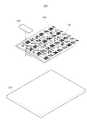
도 1은 본 발명의 일 실시예에 따른 단일 금속박막 터치패널의 분해 사시도이다.
도 2는 도 1의 단일 금속박막 터치패널에서 투명 기판의 정면도이다.
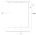
도 3은 도 2의 투명 기판 일면에 금속센싱전극부 및 금속배선전극부가 형성된 모습을 도시한 정면도이다.
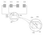
도4는 도3에서 제1 금속센싱전극과 제1 금속배선전극이 연결되는 모습을 개략적으로 도시한 개념도이다.
도 5는 본 발명의 일 실시예에 따른 단일 금속박막 터치패널 제조방법의 순서도이다.1 is an exploded perspective view of a single metal thin film touch panel according to an exemplary embodiment of the present invention.
FIG. 2 is a front view of a transparent substrate in the single metal thin film touch panel of FIG. 1.
3 is a front view illustrating a metal sensing electrode part and a metal wiring electrode part formed on one surface of the transparent substrate of FIG. 2.
FIG. 4 is a conceptual diagram schematically illustrating how the first metal sensing electrode and the first metal wiring electrode are connected to each other in FIG. 3.
5 is a flow chart of a method for manufacturing a single metal thin film touch panel according to an embodiment of the present invention.
이하, 첨부된 도면을 참조하여 본 발명의 실시예들에 대하여 상세히 설명하도록 한다.Hereinafter, embodiments of the present invention will be described in detail with reference to the accompanying drawings.
도 1은 본 발명의 일 실시예에 따른 단일 금속박막 터치패널(100)의 분해 사시도이다.1 is an exploded perspective view of a single metal thin
도 1을 참조하면, 단일 금속박막 터치패널(100)은 투명 기판(110)과, 투명 기판(110) 일면에 형성되는 금속센싱전극부(120) 및 금속배선전극부(130)와, 투명 기판(110)에 배치되어 금속배선전극부(130)가 구분되어 연결되는 접속부(140)를 포함한다.Referring to FIG. 1, the single metal thin
본 발명의 일 실시예에 따른 단일 금속박막 터치패널(100)은 센싱전극부 및 배선전극부를 단일층에 형성하면서도 상기 센싱전극부를 X축 전극 및 Y축 전극으로 구분하여 연결시킴으로써, 단일 박막을 사용하여 멀티 터치를 구현 가능하도록 한 것을 일 특징으로 한다.In the single metal thin
또한, 상기 센싱전극부 및 배선전극부를 종래 ITO(Indium Tin Oxide)를 대체하여 금속으로 형성함으로써 전극들 간의 저항을 감소시킬 뿐만 아니라, 가격 경쟁력을 향상시키고 공정을 단순화 시킨 것을 일 특징으로 한다.In addition, the sensing electrode portion and the wiring electrode portion by replacing the conventional indium tin oxide (ITO) to form a metal, not only to reduce the resistance between the electrodes, but also to improve the price competitiveness and simplifies the process.
이하에서는, 단일 금속박막 터치패널(100)의 각 구성에 대하여 설명하도록 한다.Hereinafter, each configuration of the single metal thin
도 2는 도 1의 단일 금속박막 터치패널(100)에서 투명 기판(110)의 정면도이다.FIG. 2 is a front view of the
도 2를 참조하면, 투명 기판(110)은 금속센싱전극부(120), 금속배선전극부(130) 및 접속부(140)를 지지하는 역할을 수행한다. 투명 기판(110)은 SiO2를 주성분으로 하는 유리기판 또는 강화유리기판이 사용될 수 있으며, 경우에 따라 투명 실리콘 기판 내지는 투명 플라스틱 기판을 사용하는 것도 가능하다.Referring to FIG. 2, the
투명 기판(110)은 활성 영역(110A, Active area) 및 비활성 영역(110B, Non-active area)을 구비할 수 있다. 여기에서 활성 영역(110A)은 터치패널 중 사용자의 신체 접촉 또는 별도의 터치 도구(예를 들면, 스타일러스 펜)를 이용하여 접촉 위치를 감지하는 영역에 해당하고, 비활성 영역(110B)은 활성 영역(110A)를 제외한 영역으로 주로 활성 영역(110A)에서 감지한 접속 신호를 컨트롤러 IC(집적회로) 등에 전달하는 영역에 해당한다.The
활성 영역(110A)에는 금속센싱전극부(120)가 형성되어 접촉 위치를 감지하게 되고, 활성 영역(110A) 또는 비활성 영역(110B)에는 금속센싱전극부(120)를 전기적으로 연결하는 금속배선전극부(130)가 형성된다.A
종래에는 배선전극부가 비활성 영역(110B)에만 형성되었으나, 본 발명의 일 실시예에 따른 단일 금속박막 터치패널(100)에서는 비활성 영역(110B)뿐만 아니라 활성 영역(110A)에도 금속배선전극부(130)를 형성함으로써 단일층에 센싱전극 및 배선전극을 모두 형성시킨 것을 일 특징으로 한다.Conventionally, although the wiring electrode part is formed only in the
한편, 투명 기판(110)은 투명 기판(110)과 금속센싱전극부(120) 사이에 배치되는 헤이즈(haze)층(미도시)을 더 포함할 수 있다. 상기 헤이즈층은 외부에서 들어오는 빛이 금속센싱전극부(120)에 반사되어 발생하는 레인보우 현상을 최소화 하는 역할을 수행한다. 상기 헤이즈층은 헤이즈(haze) 특성을 갖는 수지 조성물을 코팅하거나 기판 유리를 에칭함으로써 형성될 수 있다.The
도 3은 도 2의 투명 기판(100) 일면에 금속센싱전극부(120) 및 금속배선전극부(130)가 형성된 모습을 도시한 정면도이다.3 is a front view illustrating a
도 3을 참조하면, 금속센싱전극부(120)는 투명 기판(100)의 활성 영역(110A)에 제 1 방향으로 배치되는 제1 금속센싱전극(121)과 상기 제1 방향과 교번하여 제2 방향으로 배치되는 제2 금속센싱전극(123)을 복수 개 구비할 수 있다.Referring to FIG. 3, the metal
본 발명의 일 실시예에 따른 단일 금속박막 터치패널(100)은 종래 ITO를 대체하여 센싱전극들을 금속으로 형성함으로써 터치패널의 검출강도를 향상시키고, 제품 가격 경쟁력을 향상시킨 것을 일 특징으로 한다.The single metal thin
여기에서 제1 금속센싱전극(121) 및 제2 금속센싱전극(123)은 Ag, Al, Cu, Cr, Ni, Mo 중 어느 하나 또는 이들의 합금으로 제조될 수 있다.The first
한편, 도 3에 도시된 바와 같이, 상기 제1 방향은 단일 금속박막 터치패널(100)의 정면 우측을 기준으로 홀수 열(1열, 3열, 5열, 7열)에 해당할 수 있으며, 상기 제2 방향은 상기 제1 방향과 교번하는 짝수 열(2열, 4열, 6열 순)일 수 있다.On the other hand, as shown in Figure 3, the first direction may correspond to odd columns (1 column, 3 columns, 5 columns, 7 columns) with respect to the front right of the single metal thin
상기 제1 방향 및 상기 제2 방향은 이에 한정되지 아니하고 다른 방향도 가능하나, 설명의 편의를 위해서 이하에서는 상기 제1 방향은 단일 금속박막 터치패널(100)의 정면 우측을 기준으로 홀수 열 방향이고, 상기 제2 방향은 짝수 열 방향인 경우를 중심으로 설명하도록 한다.The first direction and the second direction are not limited thereto, but other directions are possible, but for convenience of description, the first direction is an odd column direction based on the front right side of the single metal thin
또한, 상기 제1 방향으로 배치되는 제1 금속센싱전극(121)은 X축 전극으로 기능하고, 상기 제2 방향으로 배치되는 제2 금속센싱전극(123)은 Y축 전극으로 기능할 수 있으며 이에 대해서는 후술하기로 한다.In addition, the first
제1 금속센싱전극(121) 및 제2 금속센싱전극(123)은 세선(細線)들로 구성된 그물망(MESH) 형상으로 형성된다. 제1 금속센싱전극(121) 및 제2 금속센싱전극(123)을 세선들로 구성된 그물망 형상으로 형성함으로써, 종래 패턴 전극(센싱 전극)이 존재하는 영역과 존재하지 않는 영역 사이의 투과율 차이로 인한 패터닝 자국이 보이는 현상을 감소시킬 수 있으며, 이는 터치패널의 투과성을 향상시키는 효과를 가져올 수 있다.The first
이 때, 제1 금속센싱전극(121) 및 제2 금속센싱전극(123)에서 상기 세선들은 선폭이 1 내지 20㎛일 수 있다. 선폭이 1㎛보다 좁은 경우에는 터치패널의 생산 수율이 다소 떨어질 수 있으며, 선폭이 20㎛보다 넓은 경우에는 터치패널의 투과성 향상 효과가 떨어질 수 있다.In this case, the thin lines of the first
또한, 상기 세선들의 선들 사이의 간격은 100㎛ 이상일 수 있다. 선들 사이의 간격이 100㎛ 미만인 경우에는 터치패널의 투과율이 목적한 것보다 감소할 수 있다.In addition, an interval between the lines of the thin lines may be 100 μm or more. If the spacing between the lines is less than 100 μm, the transmittance of the touch panel may be reduced than desired.
제1 금속센싱전극(121) 및 제2 금속센싱전극(123)은 서로 겹치지 않도록 배치되고, 제1 금속센싱전극(121) 및 제2 금속센싱전극(123)의 모양은 특정 모양으로 한정되지 않는다. 예를 들면, 제1 금속센싱전극(121) 및 제2 금속센싱전극(123)은 마름모, 정사각형, 직사각형, 원 또는 정형화되지 않은 모양(예를 들면, 덴드라이트(dendrite) 구조와 같이 나뭇가지들이 얽혀 있는 모양)등으로 형성 가능하다. 다만, 설명의 편의를 위하여 이하에서는 제1 금속센싱전극(121) 및 제2 금속센싱전극(123)이 직사각형 모양으로 형성된 경우를 중심으로 설명하기로 한다.The first
금속배선전극부(130)는 투명 기판(110)의 활성 영역(110A) 또는 비활성 영역(110B)에 형성되고, 제1 금속센싱전극(121)을 전기적으로 연결시키는 제1 금속배선전극(131)과 제2 금속센싱전극(123)을 전기적으로 연결시키는 제2 금속배선전극(133)을 복수 개 구비할 수 있다.The
여기에서 제1 금속배선전극(131) 및 제2 금속배선전극(133)은 Ag, Al, Cu, Cr, Ni Mo 중 어느 하나 또는 이들의 합금으로 제조될 수 있다. 한편, 금속센싱전극부(120) 및 금속배선전극부(130)는 동일 금속 내지 합금으로 제조될 수 있으며, 이는 터치패널의 제조공정을 단순화시키는 효과를 가져올 수 있다.The first
금속배선전극부(130)는 사용자가 외부에서 물리적 접촉을 하거나 별도의 터치 도구를 사용하여 접촉하였을 때, 금속센싱전극부(120)에서 발생한 전기적 신호를 컨트롤러 IC(미도시) 또는 접속부(140)에 전달하는 역할을 수행한다.The metal
예를 들면, 도3에 도시된 바와 같이 1열, 3열, 5열, 7열에 형성된 제1 금속센싱전극(121)은 별개의 제1 금속배선전극(131)과 전기적으로 연결되어 접속부(140)에 접속된다. 한편, 2열, 4열, 6열에 형성된 제2 금속센싱전극(123) 역시 별개의 제2 금속배선전극(132)과 전기적으로 연결되어 접속부(140)에 접속된다.For example, as shown in FIG. 3, the first
이 때, 투명 기판(110) 중앙부에 형성된 금속센싱전극부(120)의 경우에는 금속배선전극부(130)를 투명 기판(110)의 활성 영역(110A)에 형성하는 것이 가능하다.In this case, in the case of the
예를 들어, 3열에 형성된 제1 금속센싱전극(121)과 5열에 형성된 제1 금속센싱전극(121)을 제1 금속배선전극(131)으로 X축 방향으로 연결하되, 상기 제1 금속배선전극(131)이 접속부(140)에 도달하는 경로를 투명 기판(110)의 활성 영역(110A)에 형성하는 것이 가능하다. 한편, 4열에 형성된 제2 금속센싱전극(123)과 연결되는 제2 금속배선전극(133)도 마찬가지로 투명 기판(110)의 활성 영역(110A)에 형성하는 것이 가능하고, 이 때의 제2 금속배선전극(133)의 형성 경로는 제1 금속배선전극(131)의 형성 경로와 겹치지 않도록 금속센싱전극들을 우회하여 형성될 수 있다.For example, the first
한편, 금속센싱전극부(120) 및 금속배선전극부(130) 상부에는 헤이즈 제거층(미도시)이 형성될 수 있다. 상기 헤이즈 제거층은 금속센싱전극부(120) 및 금속배선전극부(130)에서 발생 가능한 레인보우를 최소화하는 역할을 수행한다. 상기 헤이즈 제거층은 유기 막을 도포하거나, 광학용 유기접착제가 코팅된 플라스틱 필름을 접합하여 헤이즈 제거층을 형성할 수 있다.Meanwhile, a haze removing layer (not shown) may be formed on the
접속부(140)는 투명 기판(110)의 비활성 영역(110B)에 배치되어 복수 개의 금속배선전극부(130)를 구분 및 연결하는 역할을 수행한다. 접속부(140)는 예를 들면, 2층 이상의 회로층으로 구성되는 다층인쇄회로기판일 수 있다. 상기 다층 인쇄회로기판의 예로는 양쪽 면에 회로층을 형성한 양면 PCB(Prited Circuit Board) 또는 다층으로 배선한 MLB(Multi Layered Board)등을 들 수 있다.The
이하에서는, 금속센싱전극부(120)와 금속배선전극부(130)의 연결에 대하여 설명하도록 한다.Hereinafter, the connection between the metal
도4는 도3에서 제1 금속센싱전극(121)과 제2 금속배선전극(131)이 연결되는 모습을 개략적으로 도시한 개념도이다.4 is a conceptual diagram schematically illustrating how the first
도 3 및 도 4를 참조하여 예시하면, 1열에 형성된 제1 금속센싱전극(121a)을 전기적으로 연결하는 제1 금속배선전극(131a), 3열 및 5열에 형성된 제1 금속센싱전극(121b, 121c)을 전기적으로 연결하는 제1 금속배선전극(131b), 7열에 형성된 제1 금속센싱전극(121c)을 전기적으로 연결하는 제1 금속배선전극(131c)은 접속부(140)에 형성되어 있는 복수 개의 접속홀(미표기)을 통해 각각 접속된다. 상기 제1 금속센싱전극(121a, 121b, 121c, 121d)들은 동일한 행에 위치하는 금속센싱전극으로, 제1 금속배선전극(131a, 131b, 131c)들에 의해 전기적으로 일체화되어 X축 전극으로 기능할 수 있다.Referring to FIGS. 3 and 4, the first
상기 접속홀은 접속부(140) 내부에서 일부가 전기적으로 연결되어 있다. 예를 들면, 접속부(140) 내부에서 일정 위치에 해당하는 접속홀들끼리는 모두 전기적으로 연결된다. 따라서 각각의 제1 금속배선전극(131a, 131b, 131c)을 특정 위치에 존재하는 상기 접속홀에 각각 접속시킬 경우에, 별개로 접속된 제1 금속배선전극(131a, 131b, 131c)들은 접속부(140) 내부에서 전기적으로 일체화되어 연결된다. 즉, 접속부(140) 내부에서 1열, 3열, 5열, 7열에 형성된 제1 금속센싱전극(121)이 전기적으로 일체화되어 연결되어 X축 전극으로 기능하는 것이 가능하다.A portion of the connection hole is electrically connected in the
한편, 도4에 도시되지는 않았으나 2열, 4열 및 6열에 형성된 제2 금속센싱전극(123)과 각각 전기적으로 연결되는 제2 금속배선전극(133)은 접속부(140) 내부에서 전기적으로 일체화되지 않아도 무방하다.Although not shown in FIG. 4, the second
상술한 바와 같이, 본 발명의 일 실시예에 따른 단일 금속박막 터치패널(100)은 접속부(140) 내에서 복수 개의 제1 금속센싱전극(121)이 X축 전극으로 기능할 수 있도록 연결시킴으로써, 단일층에 형성되어 있는 제1 금속센싱전극(121)과 제2 금속센싱전극(123)을 각각 X축 전극 및 Y축 전극으로 기능하도록 할 수 있다.As described above, the single metal thin
이하에서는 단일 금속박막 터치패널의 제조방법에 관하여 설명하기로 한다.Hereinafter, a method of manufacturing a single metal thin film touch panel will be described.
도 5는 본 발명의 일 실시예에 따른 단일 금속박막 터치패널 제조방법의 순서도이다.5 is a flow chart of a method for manufacturing a single metal thin film touch panel according to an embodiment of the present invention.
도 5를 참조하면, 우선, 활성 영역(110A) 및 비활성 영역(110B)을 구비하는 투명 기판(110)을 준비하고(S110), 투명 기판(110) 일면에 금속 박막을 코팅한다. 상기 코팅은 sputter system, E-Beam system , Thermal system 또는 프린팅 공정을 이용할 수 있다. 상기 금속 박막은 Ag, Al, Cu, Cr, Ni, Mo 중 어느 하나 또는 이들의 합금으로 형성된다(S120).Referring to FIG. 5, first, a
한편, 투명 기판(110) 일면에 상기 금속 박막을 코팅하기 이전에, 헤이즈 특성을 갖는 수지 조성물을 코팅하여 헤이즈층을 형성하거나 투명기판을 에칭하여 헤이즈층을 형성 시킬 수 있다(S112).Meanwhile, before coating the metal thin film on one surface of the
다음으로, 상기 금속박막 상부에 포토레지스트 조성물을 코팅하고, 노광 공정을 이용하여 투명 기판(110)의 활성 영역(110A)에 그물망(MESH) 형상의 금속센싱전극부(120) 및 금속배선전극부(130)를 동시에 형성한다. 금속센싱전극부(120) 및 금속배선전극부(130)는 상기에서 설명한 바와 동일하므로, 여기에서는 설명을 생략하도록 한다. 본 발명의 일 실시예에 따른 단일 금속박막 터치패널 제조방법에서는 센싱 전극과 배선 전극을 동일층으로 동시에 형성함으로써 보다 터치패널 제조공정을 단순화 시킬 수 있는 것을 일 특징으로 한다(S130).Next, the photoresist composition is coated on the metal thin film, and the metal
한편, 금속센싱전극부(120) 및 금속배선전극부(130) 상부에 유기 막을 도포하여 헤이즈 제거층을 형성 또는 광학용 유기접착제가 코팅된 플라스틱 필름을 접합하여 헤이즈 제거층을 형성시킬 수 있다(S132).Meanwhile, an organic film may be coated on the
다음으로, 투명 기판(110)의 하부 비활성 영역(110B)에 접속부(140)를 배치하여 금속배선전극부(130)를 접속시킨다. 이 때, 접속부(140) 내부에서는 X축 센싱 전극으로 기능하는 금속센싱전극들이 전기적으로 연결됨으로써, 단일층에 형성된 금속센싱전극부(120)를 X축 및 Y축 센싱 전극으로 구분시켜 기능하도록 할 수 있다(S140).Next, the
이상, 본 발명의 실시예들에 대하여 설명하였으나, 해당 기술 분야에서 통상의 지식을 가진 자라면 특허청구범위에 기재된 본 발명의 사상으로부터 벗어나지 않는 범위 내에서, 구성 요소의 부가, 변경, 삭제 또는 추가 등에 의해 본 발명을 다양하게 수정 및 변경시킬 수 있을 것이며, 이 또한 본 발명의 권리범위 내에 포함된다고 할 것이다.While the present invention has been particularly shown and described with reference to exemplary embodiments thereof, many modifications and changes may be made by those skilled in the art without departing from the spirit and scope of the invention as defined in the appended claims. The present invention can be variously modified and changed by those skilled in the art, and it is also within the scope of the present invention.
100: 터치패널
110: 투명 기판110A: 활성 영역
110B: 비활성 영역120: 금속센싱전극부
121: 제1금속센싱전극123: 제2금속센싱전극
130: 금속배선전극부131: 제1금속배선전극
132: 제2금속배선전극140: 접속부100: touch panel
110:
110B: inactive region 120: metal sensing electrode portion
121: first metal sensing electrode 123: second metal sensing electrode
130: metal wiring electrode portion 131: first metal wiring electrode
132: second metal wiring electrode 140: connecting portion
Claims (9)
Translated fromKorean상기 투명 기판(110)의 활성 영역에 가로축 방향으로 배치되는 그물망(MESH) 형상의 제1 금속센싱전극(121)과, 상기 제1 금속센싱전극(121)과 교번하여 세로축 방향으로 배치되는 그물망(MESH) 형상의 제2 금속센싱전극(123)을 동일 평면 상에 복수 개 구비하는 금속센싱전극부(120);
최외곽에 배치된 상기 제1 금속센싱전극(121)으로부터 하기 접속부(140)까지 각각 상기 비활성 영역 상에 연장 형성되는 금속배선과, 최외곽에 배치되지 않은 동일한 가로축의 이웃하는 두 개의 상기 제1 금속센싱전극(121)을 직렬 연결하고 그 중 어느 하나의 제1 금속센싱전극(121)으로부터 하기 접속부(140)까지 각각 상기 활성 영역 상에 연장 형성되는 금속배선을 구비하는 제1 금속배선전극(131)과, 최외곽에 배치된 동일한 세로축의 상기 제2 금속센싱전극(123)들을 직렬 연결하여 하기 접속부(140)까지 연장 형성되는 금속배선과, 최외곽에 배치되지 않은 동일한 세로축의 상기 제2 금속센싱전극(123)들을 상기 활성 영역 상에서 병렬 연결하여 하기 접속부(140)까지 연장 형성되되 상기 활성 영역 상에 형성되는 제1 금속배선전극(131)과 중첩되지 않도록 독립적으로 배치되는 금속배선을 구비하는 제2 금속배선전극(133)을 포함하는 금속배선전극부(130); 및
상기 투명 기판(110)의 비활성 영역에 배치되어 복수 개의 상기 금속배선전극부(130)가 구분되어 연결되는 접속부(140)를 포함하는 단일 금속박막 터치패널.
A transparent substrate 110 having an active region and an inactive region;
A first metal sensing electrode 121 having a mesh shape (MESH) disposed in an active area of the transparent substrate 110 in the horizontal axis direction, and a mesh disposed in the vertical axis direction alternately with the first metal sensing electrode 121 ( A metal sensing electrode unit 120 having a plurality of MESH-shaped second metal sensing electrodes 123 on the same plane;
Metal wires extending from the first metal sensing electrode 121 disposed at the outermost side to the connection portion 140, respectively, on the inactive region, and two adjacent first adjacent horizontal axes not disposed at the outermost side. A first metal wiring electrode having a metal wiring extending from the first metal sensing electrode 121 and any one of the first metal sensing electrodes 121 to the following connecting portion 140 to the active region, respectively; 131 and the second metal sensing electrodes 123 having the same vertical axis disposed in the outermost part in series to extend to the connection portion 140 below, and the second vertical axis not disposed in the outermost part. The metal sensing electrodes 123 are connected in parallel on the active area to extend to the following connection part 140, but independent from the first metal wiring electrode 131 formed on the active area. Metal wiring electrode part 130 including a second metal wiring electrode 133 having a metal wiring disposed in; And
A single metal thin film touch panel including a connection part 140 disposed in an inactive region of the transparent substrate 110 to connect a plurality of the metal wiring electrode parts 130 to each other.
상기 제1 금속센싱전극(121) 및 상기 제2 금속센싱전극(123)은 1 내지 20㎛의 선폭을 가지고, 선들 사이의 간격이 100㎛ 이상인 세선(細線)들로 형성된 단일 금속박막 터치패널.
The method according to claim 1,
The first metal sensing electrode 121 and the second metal sensing electrode 123 have a line width of 1 to 20 μm and are formed of thin wires having intervals of 100 μm or more.
상기 투명 기판과 상기 금속센싱전극부(120) 사이에 배치되는 헤이즈층; 및
상기 금속센싱전극부(120) 및 금속배선전극부(130) 상부에 배치되는 헤이즈 제거층을 더 포함하는 단일 금속박막 터치패널.
The method according to claim 1,
A haze layer disposed between the transparent substrate and the metal sensing electrode unit 120; And
Single metal thin film touch panel further comprises a haze removal layer disposed on the metal sensing electrode 120 and the metal wiring electrode 130.
상기 접속부(140)는 금속센싱전극부를 축 방향으로 연결하기 위하여 2층 이상의 회로층으로 구성되는 다층인쇄회로기판인 단일 금속박막 터치패널.
The method according to claim 1,
The connection part 140 is a single metal thin film touch panel which is a multilayer printed circuit board composed of two or more circuit layers for connecting the metal sensing electrode part in an axial direction.
상기 금속 박막을 패터닝하여 상기 투명 기판의 활성 영역에 배치되는 그물망(MESH) 형상의 금속센싱전극부 및 상기 금속센싱전극부를 전기적으로 연결시키는 금속배선전극부를 동시에 형성하는 제2 단계; 및
상기 투명 기판의 비활성 영역에 접속부를 배치하여 상기 금속배선전극부를 구분하여 연결하는 제3 단계를 포함하고,
상기 금속센싱전극부는 상기 투명 기판의 활성 영역에 가로축 방향으로 배치되는 그물망(MESH) 형상의 제1 금속센싱전극 및 상기 제1 금속센싱전극과 교번하여 세로축 방향으로 배치되는 그물망(MESH) 형상의 제2 금속센싱전극을 동일 평면 상에 복수 개 구비하고,
상기 금속배선전극부는 최외곽에 배치된 상기 제1 금속센싱전극(121)으로부터 하기 접속부(140)까지 각각 상기 비활성 영역 상에 연장 형성되는 금속배선과, 최외곽에 배치되지 않은 동일한 가로축의 이웃하는 두 개의 상기 제1 금속센싱전극(121)을 직렬 연결하고 그 중 어느 하나의 제1 금속센싱전극(121)으로부터 하기 접속부(140)까지 각각 상기 활성 영역 상에 연장 형성되는 금속배선을 구비하는 제1 금속배선전극(131)과, 최외곽에 배치된 동일한 세로축의 상기 제2 금속센싱전극(123)들을 직렬 연결하여 하기 접속부(140)까지 연장 형성되는 금속배선과, 최외곽에 배치되지 않은 동일한 세로축의 상기 제2 금속센싱전극(123)들을 상기 활성 영역 상에서 병렬 연결하여 하기 접속부(140)까지 연장 형성되되 상기 활성 영역 상에 형성되는 상기 제1 금속배선전극(131)과 중첩되지 않도록 독립적으로 배치되는 금속배선을 구비하는 제2 금속배선전극(133)을 포함하는 형태로 형성되는 단일 금속박막 터치패널 제조방법.
Coating a metal thin film on one surface of the transparent substrate having an active region and an inactive region;
Patterning the metal thin film to simultaneously form a metal sensing electrode portion having a mesh shape (MESH) disposed in an active region of the transparent substrate and a metal wiring electrode portion electrically connecting the metal sensing electrode portion; And
And arranging a connection unit in an inactive region of the transparent substrate to separate and connect the metal wiring electrode units.
The metal sensing electrode part may be formed of a first metal sensing electrode having a mesh (MESH) shape disposed in an active region of the transparent substrate in a horizontal axis direction, and a mesh (MESH) shaped material disposed alternately with the first metal sensing electrode in a vertical axis direction. 2 provided with a plurality of metal sensing electrodes on the same plane,
The metal wiring electrode part may be formed on the inactive region from the first metal sensing electrode 121 disposed at the outermost side to the connection portion 140, respectively, and adjacent to the same horizontal axis not disposed at the outermost side. A second wiring including two first metal sensing electrodes 121 connected in series and extending from one of the first metal sensing electrodes 121 to the following connecting portion 140 on the active region, respectively; The first metal wiring electrode 131 and the second metal sensing electrodes 123 having the same vertical axis disposed in the outermost part are connected in series to extend the metal wiring electrode 123 to the following connecting part 140, and the same not disposed at the outermost part. The second metal sensing electrodes 123 of the vertical axis are connected in parallel on the active area to extend to the following connection part 140, but the first metal wiring electrode 13 is formed on the active area. 1) A method of manufacturing a single metal thin film touch panel, which is formed in a form including a second metal wiring electrode 133 having a metal wiring disposed independently so as not to overlap with 1).
상기 제1 단계 이전에,
상기 투명 기판 일면에 헤이즈층을 형성하는 단계;를 더 포함하고,
상기 제2단계 이후에,
상기 금속센싱전극부 및 금속배선전극부 상부에 헤이즈 제거층을 형성하는 단계;를 더 포함하는 단일 금속박막 터치패널 제조방법.
8. The method of claim 7,
Prior to the first step,
Forming a haze layer on one surface of the transparent substrate;
After the second step,
And forming a haze removing layer on the metal sensing electrode part and the metal wiring electrode part.
Priority Applications (1)
| Application Number | Priority Date | Filing Date | Title |
|---|---|---|---|
| KR1020110066465AKR101381729B1 (en) | 2011-07-05 | 2011-07-05 | Touch panel using monolithic metallic thin-film and manufature method thereof |
Applications Claiming Priority (1)
| Application Number | Priority Date | Filing Date | Title |
|---|---|---|---|
| KR1020110066465AKR101381729B1 (en) | 2011-07-05 | 2011-07-05 | Touch panel using monolithic metallic thin-film and manufature method thereof |
Publications (2)
| Publication Number | Publication Date |
|---|---|
| KR20130005093A KR20130005093A (en) | 2013-01-15 |
| KR101381729B1true KR101381729B1 (en) | 2014-04-17 |
Family
ID=47836504
Family Applications (1)
| Application Number | Title | Priority Date | Filing Date |
|---|---|---|---|
| KR1020110066465AActiveKR101381729B1 (en) | 2011-07-05 | 2011-07-05 | Touch panel using monolithic metallic thin-film and manufature method thereof |
Country Status (1)
| Country | Link |
|---|---|
| KR (1) | KR101381729B1 (en) |
Families Citing this family (3)
| Publication number | Priority date | Publication date | Assignee | Title |
|---|---|---|---|---|
| KR101493412B1 (en) | 2013-07-16 | 2015-02-13 | 삼성디스플레이 주식회사 | Foldable touch screen panel |
| KR101682773B1 (en) | 2013-12-13 | 2016-12-05 | 주식회사 엘지화학 | Touch sensor and method for preparing the same |
| KR102226601B1 (en) | 2014-12-02 | 2021-03-15 | 삼성디스플레이 주식회사 | Touch panel and method of manufacturing the same |
Citations (2)
| Publication number | Priority date | Publication date | Assignee | Title |
|---|---|---|---|---|
| JP2009009574A (en)* | 2007-06-28 | 2009-01-15 | Sense Pad Tech Co Ltd | Capacitive-type touch panel |
| JP2010157439A (en)* | 2008-12-26 | 2010-07-15 | Teijin Ltd | Transparent conductive laminate, and transparent touch panel |
- 2011
- 2011-07-05KRKR1020110066465Apatent/KR101381729B1/enactiveActive
Patent Citations (2)
| Publication number | Priority date | Publication date | Assignee | Title |
|---|---|---|---|---|
| JP2009009574A (en)* | 2007-06-28 | 2009-01-15 | Sense Pad Tech Co Ltd | Capacitive-type touch panel |
| JP2010157439A (en)* | 2008-12-26 | 2010-07-15 | Teijin Ltd | Transparent conductive laminate, and transparent touch panel |
Also Published As
| Publication number | Publication date |
|---|---|
| KR20130005093A (en) | 2013-01-15 |
Similar Documents
| Publication | Publication Date | Title |
|---|---|---|
| JP5420709B2 (en) | Touch panel electrode structure, method and touch panel | |
| KR101373606B1 (en) | Pattern structure of the metallic thin-film touch panel | |
| US8593413B2 (en) | Sensory structure of capacitive touch panel and capacitive touch panel having the same | |
| KR101093651B1 (en) | Touch panel using metal thin film and manufacturing method thereof | |
| JP5091182B2 (en) | Touch screen panel and manufacturing method thereof | |
| KR102303214B1 (en) | Touch screen panel and manufacturing method thereof | |
| CN106802746B (en) | Touch panel and image display device including the same | |
| KR101103751B1 (en) | Touch screen panel with mesh type electrode pattern | |
| JP2016503548A (en) | Projected capacitive touch panel including a silver-containing transparent conductive layer | |
| US20170045971A1 (en) | Touch screen panel | |
| KR20120018059A (en) | Substrate for touch screen panel, touch screen panel and manufacturing method thereof | |
| KR101161146B1 (en) | Touch panel using metallic thin-film and manufacture method thereof | |
| KR20160085392A (en) | Touch screen panel comprising touch sensor | |
| TWI663538B (en) | Capacitive touch panel and display device comprising the same | |
| JP5599940B2 (en) | Capacitive touch sensor system, production process thereof, and touch sensor device using the same | |
| KR101381729B1 (en) | Touch panel using monolithic metallic thin-film and manufature method thereof | |
| WO2016002461A1 (en) | Input device and method for manufacturing same | |
| JP6568537B2 (en) | Capacitive touch panel | |
| KR101294341B1 (en) | Capacitive Touch Panel | |
| KR20140016623A (en) | Touch screen panel and the method for fabricating of the same | |
| JP2013156725A (en) | Touch panel and display device | |
| KR101496254B1 (en) | Touch Panel and Method for Making the Same | |
| KR20110136118A (en) | Manufacturing Method of Touch Panel Sensor and Touch Panel Sensor | |
| KR20150019571A (en) | Touch Panel and Method for Making the Same | |
| JP3162771U (en) | Capacitive touch screen / touch panel with one-dimensional contact point position detection |
Legal Events
| Date | Code | Title | Description |
|---|---|---|---|
| A201 | Request for examination | ||
| PA0109 | Patent application | Patent event code:PA01091R01D Comment text:Patent Application Patent event date:20110705 | |
| PA0201 | Request for examination | ||
| PG1501 | Laying open of application | ||
| E902 | Notification of reason for refusal | ||
| PE0902 | Notice of grounds for rejection | Comment text:Notification of reason for refusal Patent event date:20130130 Patent event code:PE09021S01D | |
| AMND | Amendment | ||
| E902 | Notification of reason for refusal | ||
| PE0902 | Notice of grounds for rejection | Comment text:Notification of reason for refusal Patent event date:20130730 Patent event code:PE09021S01D | |
| AMND | Amendment | ||
| E601 | Decision to refuse application | ||
| PE0601 | Decision on rejection of patent | Patent event date:20140129 Comment text:Decision to Refuse Application Patent event code:PE06012S01D Patent event date:20130730 Comment text:Notification of reason for refusal Patent event code:PE06011S01I Patent event date:20130130 Comment text:Notification of reason for refusal Patent event code:PE06011S01I | |
| X091 | Application refused [patent] | ||
| AMND | Amendment | ||
| PX0901 | Re-examination | Patent event code:PX09011S01I Patent event date:20140129 Comment text:Decision to Refuse Application Patent event code:PX09012R01I Patent event date:20130926 Comment text:Amendment to Specification, etc. Patent event code:PX09012R01I Patent event date:20130321 Comment text:Amendment to Specification, etc. | |
| PX0701 | Decision of registration after re-examination | Patent event date:20140327 Comment text:Decision to Grant Registration Patent event code:PX07013S01D Patent event date:20140310 Comment text:Amendment to Specification, etc. Patent event code:PX07012R01I Patent event date:20140129 Comment text:Decision to Refuse Application Patent event code:PX07011S01I Patent event date:20130926 Comment text:Amendment to Specification, etc. Patent event code:PX07012R01I Patent event date:20130321 Comment text:Amendment to Specification, etc. Patent event code:PX07012R01I | |
| X701 | Decision to grant (after re-examination) | ||
| GRNT | Written decision to grant | ||
| PR0701 | Registration of establishment | Comment text:Registration of Establishment Patent event date:20140331 Patent event code:PR07011E01D | |
| PR1002 | Payment of registration fee | Payment date:20140401 End annual number:3 Start annual number:1 | |
| PG1601 | Publication of registration | ||
| FPAY | Annual fee payment | Payment date:20161229 Year of fee payment:4 | |
| PR1001 | Payment of annual fee | Payment date:20161229 Start annual number:4 End annual number:4 | |
| FPAY | Annual fee payment | Payment date:20171207 Year of fee payment:5 | |
| PR1001 | Payment of annual fee | Payment date:20171207 Start annual number:5 End annual number:5 | |
| FPAY | Annual fee payment | Payment date:20190304 Year of fee payment:6 | |
| PR1001 | Payment of annual fee | Payment date:20190304 Start annual number:6 End annual number:6 | |
| FPAY | Annual fee payment | Payment date:20200115 Year of fee payment:7 | |
| PR1001 | Payment of annual fee | Payment date:20200115 Start annual number:7 End annual number:7 | |
| PR1001 | Payment of annual fee | Payment date:20210120 Start annual number:8 End annual number:8 | |
| PR1001 | Payment of annual fee | Payment date:20221219 Start annual number:10 End annual number:10 | |
| PR1001 | Payment of annual fee | Payment date:20231227 Start annual number:11 End annual number:11 | |
| PR1001 | Payment of annual fee | Payment date:20241224 Start annual number:12 End annual number:12 |