KR101381610B1 - Bending method of liquid crystal display device - Google Patents
Bending method of liquid crystal display deviceDownload PDFInfo
- Publication number
- KR101381610B1 KR101381610B1KR1020120097893AKR20120097893AKR101381610B1KR 101381610 B1KR101381610 B1KR 101381610B1KR 1020120097893 AKR1020120097893 AKR 1020120097893AKR 20120097893 AKR20120097893 AKR 20120097893AKR 101381610 B1KR101381610 B1KR 101381610B1
- Authority
- KR
- South Korea
- Prior art keywords
- liquid crystal
- crystal cell
- polarizing film
- display device
- bending
- Prior art date
- Legal status (The legal status is an assumption and is not a legal conclusion. Google has not performed a legal analysis and makes no representation as to the accuracy of the status listed.)
- Active
Links
Images


Classifications
- G—PHYSICS
- G02—OPTICS
- G02F—OPTICAL DEVICES OR ARRANGEMENTS FOR THE CONTROL OF LIGHT BY MODIFICATION OF THE OPTICAL PROPERTIES OF THE MEDIA OF THE ELEMENTS INVOLVED THEREIN; NON-LINEAR OPTICS; FREQUENCY-CHANGING OF LIGHT; OPTICAL LOGIC ELEMENTS; OPTICAL ANALOGUE/DIGITAL CONVERTERS
- G02F1/00—Devices or arrangements for the control of the intensity, colour, phase, polarisation or direction of light arriving from an independent light source, e.g. switching, gating or modulating; Non-linear optics
- G02F1/01—Devices or arrangements for the control of the intensity, colour, phase, polarisation or direction of light arriving from an independent light source, e.g. switching, gating or modulating; Non-linear optics for the control of the intensity, phase, polarisation or colour
- G02F1/13—Devices or arrangements for the control of the intensity, colour, phase, polarisation or direction of light arriving from an independent light source, e.g. switching, gating or modulating; Non-linear optics for the control of the intensity, phase, polarisation or colour based on liquid crystals, e.g. single liquid crystal display cells
- G02F1/133—Constructional arrangements; Operation of liquid crystal cells; Circuit arrangements
- G02F1/1333—Constructional arrangements; Manufacturing methods
- G02F1/1335—Structural association of cells with optical devices, e.g. polarisers or reflectors
- G02F1/133528—Polarisers
- G—PHYSICS
- G02—OPTICS
- G02F—OPTICAL DEVICES OR ARRANGEMENTS FOR THE CONTROL OF LIGHT BY MODIFICATION OF THE OPTICAL PROPERTIES OF THE MEDIA OF THE ELEMENTS INVOLVED THEREIN; NON-LINEAR OPTICS; FREQUENCY-CHANGING OF LIGHT; OPTICAL LOGIC ELEMENTS; OPTICAL ANALOGUE/DIGITAL CONVERTERS
- G02F1/00—Devices or arrangements for the control of the intensity, colour, phase, polarisation or direction of light arriving from an independent light source, e.g. switching, gating or modulating; Non-linear optics
- G02F1/01—Devices or arrangements for the control of the intensity, colour, phase, polarisation or direction of light arriving from an independent light source, e.g. switching, gating or modulating; Non-linear optics for the control of the intensity, phase, polarisation or colour
- G02F1/13—Devices or arrangements for the control of the intensity, colour, phase, polarisation or direction of light arriving from an independent light source, e.g. switching, gating or modulating; Non-linear optics for the control of the intensity, phase, polarisation or colour based on liquid crystals, e.g. single liquid crystal display cells
- G02F1/133—Constructional arrangements; Operation of liquid crystal cells; Circuit arrangements
- G02F1/1333—Constructional arrangements; Manufacturing methods
Landscapes
- Physics & Mathematics (AREA)
- Nonlinear Science (AREA)
- Liquid Crystal (AREA)
- Mathematical Physics (AREA)
- Chemical & Material Sciences (AREA)
- Crystallography & Structural Chemistry (AREA)
- General Physics & Mathematics (AREA)
- Optics & Photonics (AREA)
Abstract
Translated fromKoreanDescription
Translated fromKorean본 발명은 액정디스플레이 장치의 벤딩 방법에 관한 것으로서, 보다 상세하게는 초박형으로 구성되어 원하는 곡면 형태로 구부러진 액정패널의 조립 공정이 간단해지고, 구부러진 액정패널과 프레임의 정렬이 간편해지며, 액정패널에 휨응력, 진동, 충격 등과 같은 외력이 가해질 때, 액정패널이 파손되는 것을 방지할 수 있는 액정디스플레이 장치의 벤딩 방법에 관한 것이다.
The present invention relates to a bending method of a liquid crystal display device, and more particularly, an ultra-thin configuration, which simplifies the assembling process of a liquid crystal panel bent to a desired curved shape, facilitates alignment of the bent liquid crystal panel and a frame, and a bending stress on the liquid crystal panel. The present invention relates to a bending method of a liquid crystal display device that can prevent a liquid crystal panel from being damaged when an external force such as vibration, shock, or the like is applied.
일반적으로, 액정디스플레이 장치(liquid crystal display, LCD)의 액정패널 (LCD panel)은 상부기판과 하부기판 사이에 유전율 이방성(dielectric anisotropy)을 갖는 액정을 포함한다. 액정에 전계를 인가하고, 이 전계의 세기를 조절하여 액정을 통과하는 빛의 투과율을 조절함으로써 원하는 화상을 얻는다.In general, a liquid crystal panel (LCD panel) of a liquid crystal display (LCD) includes a liquid crystal having dielectric anisotropy between an upper substrate and a lower substrate. The desired image is obtained by applying an electric field to the liquid crystal and adjusting the intensity of the electric field to adjust the transmittance of light passing through the liquid crystal.
이러한 액정디스플레이 장치는 휴대가 간편한 평판표시장치(flat panel display, FPD) 중에서 대표적인 것으로서, 이 중에서도 박막 트랜지스터(thin film transistor, TFT)를 스위칭 소자로 이용한 TFT-LCD가 주로 이용되고 있다.Such liquid crystal display devices are typical among portable flat panel displays (FPDs) that are easy to carry. Among them, TFT-LCDs using thin film transistors (TFTs) as switching elements are mainly used.
이러한 액정패널은 통상 평평한 형태로 제조되므로 곡면 형태의 디스플레이가 필요한 경우 통상적인 평평한 액정패널이 사용될 수 없는 문제가 있다.Since the liquid crystal panel is generally manufactured in a flat form, when a curved display is required, a conventional flat liquid crystal panel cannot be used.
이러한 문제점을 해결하기 위해 종래의 액정패널의 유리기판 대신에 플라스틱기판 등을 사용하여 플렉시블한 액정패널의 기술개발이 전개되었으나 대형 및 고해상도에 대응할 수 없는 문제점이 존재하였다. 이러한 이유로 종래의 유리기판을 적용한 액정패널을 재가공하여 대형 및 고해상도에 대응 가능한 휘어진 액정패널의 기술개발이 전개되었다.In order to solve this problem, technology development of a flexible liquid crystal panel using a plastic substrate instead of the glass substrate of the conventional liquid crystal panel has been developed, but there was a problem that cannot cope with large size and high resolution. For this reason, the technology development of curved liquid crystal panel capable of coping with large size and high resolution by reprocessing a liquid crystal panel using a conventional glass substrate has been developed.
그러나 종래의 유리기판을 적용한 액정패널을 재가공하는 경우, 유리기판을 박형화하여 만들어진 초박형의 액정셀에 직사각형 형태의 편평한 편광필름을 부착하여 편평한 초박형 액정패널을 만들고, 상기 편평한 초박형 액정패널을 휘어진 형태로 조립하는 과정에서 균일한 벤딩이 곤란해져 배향 불균일과 셀갭 얼룩 등의 불량발생 가능성이 커지고, 용이한 벤딩이 곤란해져 벤딩 중 파손 등의 불량 발생 가능성이 커지는 문제점이 나타났다.However, when reprocessing a liquid crystal panel to which a conventional glass substrate is applied, a rectangular flat polarizing film is attached to an ultra thin liquid crystal cell made by thinning a glass substrate to form a flat ultra thin liquid crystal panel, and the flat ultra thin liquid crystal panel is curved. In the assembling process, it is difficult to uniformly bend, thereby increasing the possibility of defects such as orientation unevenness and cell gap staining, and easily bending becomes difficult, resulting in the possibility of defects such as breakage during bending.
관련 선행기술로는 대한민국 공개특허공보 제2011-0030732호 (2011. 03. 24. 공개, 발명의 명칭 : 곡면 형태의 디스플레이 패널 제조 방법) 가 있다.
Related prior art is Korean Patent Publication No. 2011-0030732 (2011. 03. 24. Publication, the name of the invention: curved display panel manufacturing method).
본 발명은 초박형으로 구성되어 원하는 곡면 형태로 구부러진 액정패널의 조립 공정이 간단해지고, 구부러진 액정패널과 프레임의 정렬이 간편해지며, 액정패널에 휨응력, 진동, 충격 등과 같은 외력이 가해질 때, 액정패널이 파손되는 것을 방지할 수 있는 액정디스플레이 장치의 벤딩 방법을 제공하는 데 목적이 있다.
According to the present invention, an ultra-thin configuration simplifies the process of assembling a liquid crystal panel bent to a desired curved shape, aligns a curved liquid crystal panel with a frame, and when an external force such as bending stress, vibration, or impact is applied to the liquid crystal panel, An object of the present invention is to provide a bending method of a liquid crystal display device that can prevent damage.
본 발명에 따른 액정디스플레이 장치의 벤딩 방법은 상부기판과 하부기판 사이에 액정이 주입되고 기설정된 두께를 갖는 액정셀의 양면에 편광필름을 결합하여 액정패널을 형성하는 부착단계; 상기 부착단계를 거친 상기 액정패널을 곡면 형태로 구부리는 벤딩단계; 상기 편광필름이 연화되도록 상기 액정패널의 표면을 가열하는 가열단계; 및 상기 가열단계를 거쳐 연화된 상기 편광필름을 냉각시키는 냉각단계; 를 포함하는 것을 특징으로 한다.Bending method of the liquid crystal display device according to the present invention comprises the attachment step of forming a liquid crystal panel by injecting a liquid crystal between the upper substrate and the lower substrate and combining the polarizing film on both sides of the liquid crystal cell having a predetermined thickness; Bending the liquid crystal panel that has undergone the attaching step into a curved shape; A heating step of heating the surface of the liquid crystal panel to soften the polarizing film; And a cooling step of cooling the polarized film softened through the heating step. And a control unit.
또한 상기 벤딩단계에서 상기 곡면 형태에 대응되는 지그를 사용하는 경우, 상기 냉각단계를 거친 상기 액정패널에서 상기 지그를 분리하는 분리단계; 를 더 포함하는 것을 특징으로 한다.In addition, when using the jig corresponding to the curved shape in the bending step, the separation step of separating the jig from the liquid crystal panel after the cooling step; And further comprising:
또한 상기 냉각단계를 거친 상기 액정패널의 양면에 각각 프레임부를 결합하는 결합단계; 를 더 포함하는 것을 특징으로 한다.In addition, the coupling step of coupling the frame portion on each side of the liquid crystal panel after the cooling step; And further comprising:
또한 상기 프레임부에는, 상기 액정패널의 단부를 지지하는 이탈방지부; 가 구비되는 것을 특징으로 한다.In addition, the frame portion, the separation prevention portion for supporting the end of the liquid crystal panel; Is provided.
또한 상기 부착단계를 거쳐 상기 액정셀에 결합된 상기 편광필름의 두께는, 상기 액정셀의 두께와 같거나 크게 형성되는 것을 특징으로 한다.In addition, the thickness of the polarizing film coupled to the liquid crystal cell through the attachment step is characterized in that the same as or larger than the thickness of the liquid crystal cell.
또한 상기 부착단계에 앞서 액정셀을 기설정된 두께로 감소시키는 박판제조단계; 를 더 포함하는 것을 특징으로 한다.In addition, a thin plate manufacturing step of reducing the liquid crystal cell to a predetermined thickness prior to the attaching step; And further comprising:
또한 상기 박판제조단계는, 상기 액정셀을 반입하는 반입단계; 및 상기 액정셀이 기설정된 두께로 감소되도록 상기 액정셀의 상부기판과 상기 하부기판을 각각 깎아내는 식각단계; 를 포함하는 것을 특징으로 한다.In addition, the thin plate manufacturing step, the import step of bringing in the liquid crystal cell; An etching step of shaving the upper substrate and the lower substrate of the liquid crystal cell so that the liquid crystal cell is reduced to a predetermined thickness; And a control unit.
또한 상기 박판제조단계는, 상기 반입단계를 거친 상기 액정셀에 상기 편광필름이 결합된 경우, 상기 반입단계를 거쳐 반입된 상기 액정셀에서 상기 편광필름을 제거하는 제거단계; 를 포함하는 것을 특징으로 한다.In addition, the thin plate manufacturing step, if the polarizing film is coupled to the liquid crystal cell passed through the carrying-in step, the removing step of removing the polarizing film from the liquid crystal cell imported through the carrying-in step; And a control unit.
또한 상기 부착단계를 거친 상기 액정패널의 가장자리를 감싸는 마감단계; 가 더 포함되는 것을 특징으로 한다.
In addition, the finishing step of wrapping the edge of the liquid crystal panel after the attachment step; Is further included.
본 발명에 따른 액정디스플레이 장치의 벤딩 방법은 초박형으로 구성되어 원하는 곡면 형태로 구부러진 액정패널의 조립 공정이 간단해지고, 구부러진 액정패널과 프레임의 정렬이 간편해지며, 액정패널에 휨응력, 진동, 충격 등과 같은 외력이 가해질 때, 액정패널이 파손되는 것을 방지할 수 있다.The bending method of the liquid crystal display device according to the present invention is configured to be ultra-thin to simplify the process of assembling the liquid crystal panel bent to the desired curved shape, the alignment of the bent liquid crystal panel and the frame is simplified, such as bending stress, vibration, impact, etc. When an external force is applied, the liquid crystal panel can be prevented from being damaged.
또한, 본 발명은 벤딩 균일성과 벤딩 용이성을 향상시킬 수 있다.In addition, the present invention can improve bending uniformity and bending ease.
또한, 본 발명은 액정패널에서 배향 불균일 또는 셀갭 얼룩 등과 같은 불량 발생 가능성을 감소시키거나 없앨 수 있다.
In addition, the present invention can reduce or eliminate the possibility of defects, such as uneven alignment or cell gap staining in the liquid crystal panel.
도 1은 본 발명의 제1실시예에 따른 액정디스플레이 장치를 개략적으로 도시한 결합단면도,
도 2는 본 발명의 제2실시예에 따른 액정디스플레이 장치를 개략적으로 도시한 결합단면도,
도 3은 본 발명의 제3실시예에 따른 액정디스플레이 장치를 개략적으로 도시한 결합단면도,
도 4는 본 발명의 제4실시예에 따른 액정디스플레이 장치를 개략적으로 도시한 결합단면도,
도 5는 본 발명의 제5실시예에 따른 액정디스플레이 장치를 개략적으로 도시한 결합단면도,
도 6은 본 발명의 일 실시예에 따른 액정디스플레이 장치의 벤딩 방법을 나타내는 순서도,
도 7은 본 발명의 일 실시예에 따른 벤딩 방법으로 제조된 액정디스플레이 장치를 도시한 결합단면도이다.1 is a cross-sectional view schematically showing a liquid crystal display device according to a first embodiment of the present invention;
2 is a cross-sectional view schematically showing a liquid crystal display device according to a second embodiment of the present invention;
3 is a cross-sectional view schematically showing a liquid crystal display device according to a third embodiment of the present invention;
4 is a cross-sectional view schematically showing a liquid crystal display device according to a fourth embodiment of the present invention;
5 is a cross-sectional view schematically showing a liquid crystal display device according to a fifth embodiment of the present invention;
6 is a flowchart illustrating a bending method of a liquid crystal display device according to an embodiment of the present invention;
7 is a cross-sectional view illustrating a liquid crystal display device manufactured by a bending method according to an embodiment of the present invention.
이하, 첨부된 도면들을 참조하여 본 발명에 따른 액정디스플레이 장치의 벤딩 방법의 일 실시예를 설명한다. 이 과정에서 도면에 도시된 선들의 두께나 구성요소의 크기 등은 설명의 명료성과 편의상 과장되게 도시되어 있을 수 있다. 또한, 후술되는 용어들은 본 발명에서의 기능을 고려하여 정의된 용어들로서 이는 사용자, 운용자의 의도 또는 관례에 따라 달라질 수 있다. 그러므로, 이러한 용어들에 대한 정의는 본 명세서 전반에 걸친 내용을 토대로 내려져야 할 것이다.
Hereinafter, with reference to the accompanying drawings will be described an embodiment of a bending method of the liquid crystal display device according to the present invention. In this process, the thicknesses of the lines and the sizes of the components shown in the drawings may be exaggerated for clarity and convenience of explanation. In addition, the terms described below are defined in consideration of the functions of the present invention, which may vary depending on the intention or custom of the user, the operator. Therefore, definitions of these terms should be made based on the contents throughout this specification.
본 발명을 설명함에 있어서, 액정패널(10)은 양면에 편광필름(30)이 결합된 액정셀(20)을 말하고, 액정셀(20)은 상부기판(21)과 하부기판(23) 사이에 액정(25)이 주입된 기판모듈을 말한다.In describing the present invention, the
또한, 두께는 액정셀(20)과 편광필름(30)의 적층 방향에 따른 길이를 의미한다. 도면에서 t0은 액정패널(10)의 두께이고, t1은 상부기판(21)의 두께이며, t2는 하부기판(23)의 두께이고, t3은 상부기판(21)과 하부기판(23) 사이의 간격으로 액정(25)의 두께이다.
In addition, the thickness means a length along the stacking direction of the
도 1은 본 발명의 제1실시예에 따른 액정디스플레이 장치를 개략적으로 도시한 결합단면도이다.1 is a cross-sectional view schematically showing a liquid crystal display device according to a first embodiment of the present invention.
도 1을 참조하면, 본 발명의 제1실시예에 따른 액정디스플레이 장치는 액정셀(20)과, 편광필름(30)과, 마감부(40)를 포함한다.Referring to FIG. 1, the liquid crystal display device according to the first embodiment of the present invention includes a
액정셀(20)은 상부기판(21)과 하부기판(23) 사이에 액정(25)이 주입된 기판모듈이다. 액정셀(20)은 초박형으로 구성되어 기설정된 두께를 갖는다. 여기서, 상부기판(21)과 하부기판(23)은 투명한 재질로 이루어질 수 있다. 또한, 상부기판(21)과 하부기판(23)은 유리 재질로 이루어질 수 있다.The
액정셀(20)은 상부기판(21)과 하부기판(23)이 기설정된 두께를 갖도록 깎아내어 초박형으로 구성할 수 있다. 또한, 액정셀(20)은 기설정된 두께를 갖는 상부기판(21)과 기설정된 두께를 갖는 하부기판(23) 사이에 액정(25)을 주입하여 초박형으로 구성할 수 있다. 여기서, 초박형의 액정셀(20)은 원하는 곡면 형태로 구부림으로써, 원하는 곡면 형태의 액정디스플레이 장치를 구현할 수 있다. 이때, 초박형의 액정셀(20) 표면에는 미세한 균열이 잔존한다.The
기설정된 액정셀(20)의 두께(t0)는 0.1mm 이상 1.0mm 이하로 이루어질 수 있다. 좀 더 구체적으로, 기설정된 액정셀(20)의 두께(t0)는 0.1mm 이상 0.4mm 이하로 이루어질 수 있다. 또한, 기설정된 액정셀(20)의 두께(t0)는 0.1mm 이상 0.5mm 이하로 이루어질 수 있다. 기설정된 액정셀(20)의 두께(t0)는 0.1mm 이상 0.8mm 이하로 이루어질 수 있다.The preset thickness t0 of the
또한, 기설정된 액정셀(20)의 두께(t0)는 0.2mm 이상 0.4mm 이하로 이루어질 수 있다. 또한, 기설정된 액정셀(20)의 두께(t0)는 0.2mm 이상 0.5mm 이하로 이루어질 수 있다. 또한, 기설정된 액정셀(20)의 두께(t0)는 0.2mm 이상 0.8mm 이하로 이루어질 수 있다. 기설정된 액정셀(20)의 두께(t0)는 0.2mm 이상 1.0mm 이하로 이루어질 수 있다. 여기서, 상부기판(21)과 하부기판(23)의 두께(t1, t2)는 각각 0.1mm 이상 0.5mm 이하로 이루어질 수 있다. 상부기판(21)과 하부기판(23)의 두께(t1, t2)는 각각 0.1mm 이상 0.4mm 이하로 이루어질 수 있다. 또한, 상부기판(21)과 하부기판(23)의 두께(t1, t2)는 각각 0.05mm 이상 0.2mm 이하로 이루어질 수 있다. 상부기판(21)과 하부기판(23)의 두께(t1, t2)는 각각 0.05mm 이상 0.25mm 이하로 이루어질 수 있다.In addition, the predetermined thickness t0 of the
두께(t0, t1, t2)의 하한값보다 작아지게 되면, 액정셀(20)을 구부리는 과정에서 액정셀(20)의 표면에 미세한 균열이 생성되거나 액정셀(20)의 표면에 잔존하는 균열의 전파를 확산시킬 수 있고, 결국에는 액정셀(20)이 파손될 수 있다. 또한, 두께(t0, t1, t2)의 상한값보다 커지게 되면, 액정셀(20)을 원하는 곡면 형태로 구부리는 것이 어렵게 된다. 따라서, 액정셀(20)의 두께(t0, t1, t2)를 한정함으로써, 초박형의 액정셀(20)을 구부릴 때, 액정셀(20)의 표면에 잔존하는 균열의 전파를 차단함은 물론 초박형의 액정셀(20)이 파손되는 것을 방지하고, 초박형의 액정셀(20)을 원하는 곡면 형태로 구부릴 수 있다.When the thickness becomes smaller than the lower limit of the thicknesses t0, t1, and t2, fine cracks are formed on the surface of the
편광필름(30)은 입사광의 수직 또는 수평 편파를 구분하여 통과시키거나 차단시킬 수 있는 성질의 필름으로, 액정셀(20)의 양면에 각각 결합된다. 여기서, 편광필름(30)은 액정셀(20)의 일측면에 결합되는 제1편광필름(31)과, 액정셀(20)의 타측에 결합되는 제2편광필름(32)으로 구분할 수 있다.The
편광필름(30)이 액정셀(20)의 양면에 결합됨으로써, 액정셀(20)의 양면에 잔존하는 균열로부터 액정셀(20)이 파손되는 것을 우선적으로 방지할 수 있다. 여기서, 편광필름(30)의 두께는 상부기판(21)의 두께(t1) 또는 하부기판(23)의 두께(t2)와 같거나 크게 이루어짐으로써, 액정셀(20)을 원하는 곡면 형태로 구부릴 때, 액정셀(20)의 곡면 형태를 안정되게 지지하고, 액정셀(20)을 보호할 수 있다.By bonding the
마감부(40)는 액정셀(20)의 가장자리를 감싸도록 액정셀(20)과 편광필름(30) 중 적어도 어느 하나에 결합된다. 본 발명의 제1실시예에서 마감부(40)는 액정셀(20)의 가장자리와 같아지도록 편광필름(30)의 가장자리에서 연장 형성되어 액정셀(20)에 결합되는 필름연장부(41)로 구성된다. 필름연장부(41)가 구비됨으로써, 액정셀(20)의 양면에 잔존하는 균열로부터 액정셀(20)이 파손되는 것을 최종적으로 방지할 수 있다.
The
지금부터는 본 발명의 제2실시예에 따른 액정디스플레이 장치에 대하여 설명한다.The liquid crystal display device according to the second embodiment of the present invention will now be described.
도 2는 본 발명의 제2실시예에 따른 액정디스플레이 장치를 개략적으로 도시한 결합단면도이다.2 is a cross-sectional view schematically showing a liquid crystal display device according to a second embodiment of the present invention.
도 2를 참조하면, 본 발명의 제2실시예에 따른 액정디스플레이 장치는 액정셀(20)과, 편광필름(30)과, 마감부(40)를 포함한다.2, a liquid crystal display device according to a second embodiment of the present invention includes a
액정셀(20)은 상부기판(21)과 하부기판(23) 사이에 액정(25)이 주입된 기판모듈이다. 액정셀(20)은 초박형으로 구성되어 기설정된 두께를 갖는다. 여기서, 상부기판(21)과 하부기판(23)은 투명한 재질로 이루어질 수 있다. 또한, 상부기판(21)과 하부기판(23)은 유리 재질로 이루어질 수 있다. 액정셀(20)은 상부기판(21)과 하부기판(23)이 기설정된 두께를 갖도록 깎아내어 초박형으로 구성하게 된다. 또한, 액정셀(20)은 기설정된 두께를 갖는 상부기판(21)과 하부기판(23) 사이에 액정(25)을 주입하여 초박형으로 구성할 수 있다. 여기서, 초박형의 액정셀(20)은 원하는 곡면 형태로 구부림으로써 곡면 디스플레이 장치를 구현할 수 있다. 이때, 초박형의 액정셀(20) 표면에는 미세한 균열이 잔존한다.The
기설정된 액정셀(20)의 두께(t0)는 0.1mm 이상 1.0mm 이하로 이루어질 수 있다. 좀 더 구체적으로, 기설정된 액정셀(20)의 두께(t0)는 0.1mm 이상 0.4mm 이하로 이루어질 수 있다. 또한, 기설정된 액정셀(20)의 두께(t0)는 0.1mm 이상 0.5mm 이하로 이루어질 수 있다. 기설정된 액정셀(20)의 두께(t0)는 0.1mm 이상 0.8mm 이하로 이루어질 수 있다.The preset thickness t0 of the
또한, 기설정된 액정셀(20)의 두께(t0)는 0.2mm 이상 0.4mm 이하로 이루어질 수 있다. 또한, 기설정된 액정셀(20)의 두께(t0)는 0.2mm 이상 0.5mm 이하로 이루어질 수 있다. 또한, 기설정된 액정셀(20)의 두께(t0)는 0.2mm 이상 0.8mm 이하로 이루어질 수 있다. 기설정된 액정셀(20)의 두께(t0)는 0.2mm 이상 1.0mm 이하로 이루어질 수 있다. 여기서, 상부기판(21)과 하부기판(23)의 두께(t1, t2)는 각각 0.1mm 이상 0.5mm 이하로 이루어질 수 있다. 상부기판(21)과 하부기판(23)의 두께(t1, t2)는 각각 0.1mm 이상 0.4mm 이하로 이루어질 수 있다. 또한, 상부기판(21)과 하부기판(23)의 두께(t1, t2)는 각각 0.05mm 이상 0.2mm 이하로 이루어질 수 있다. 상부기판(21)과 하부기판(23)의 두께(t1, t2)는 각각 0.05mm 이상 0.25mm 이하로 이루어질 수 있다.In addition, the predetermined thickness t0 of the
두께(t0, t1, t2)의 하한값보다 작아지게 되면, 액정셀(20)을 구부리는 과정에서 액정셀(20)의 표면에 미세한 균열이 생성되거나 액정셀(20)의 표면에 잔존하는 균열의 전파를 확산시킬 수 있고, 결국에는 액정셀(20)이 파손될 수 있다. 또한, 두께(t0, t1, t2)의 상한값보다 커지게 되면, 액정셀(20)을 원하는 곡면 형태로 구부리는 것이 어렵게 된다. 따라서, 액정셀(20)의 두께(t0, t1, t2)를 한정함으로써, 초박형의 액정셀(20)을 구부릴 때, 액정셀(20)의 표면에 잔존하는 균열의 전파를 차단함은 물론 초박형의 액정셀(20)이 파손되는 것을 방지하고, 초박형의 액정셀(20)을 원하는 곡면 형태로 구부릴 수 있다.When the thickness becomes smaller than the lower limit of the thicknesses t0, t1, and t2, fine cracks are formed on the surface of the
편광필름(30)은 입사광의 수직 또는 수평 편파를 구분하여 통과시키거나 차단시킬 수 있는 성질의 필름으로, 액정셀(20)의 양면에 각각 결합된다.The
여기서, 편광필름(30)은 액정셀(20)의 일측면에 결합되는 제1편광필름(31)과, 액정셀(20)의 타측에 결합되는 제2편광필름(32)으로 구분할 수 있다. 편광필름(30)이 액정셀(20)의 양면에 결합됨으로써, 액정셀(20)의 양면에 잔존하는 균열로부터 액정셀(20)이 파손되는 것을 우선적으로 방지할 수 있다. 여기서, 편광필름(30)의 두께는 상부기판(21)의 두께(t1) 또는 하부기판(23)의 두께(t2)와 같거나 크게 이루어짐으로써, 액정셀(20)을 원하는 곡면 형태로 구부릴 때, 액정셀(20)의 곡면 형태를 안정되게 지지하고, 액정셀(20)을 보호할 수 있다.Here, the
마감부(40)는 액정셀(20)의 가장자리를 감싸도록 액정셀(20)과 편광필름(30) 중 적어도 어느 하나에 결합된다. 본 발명의 제2실시예에 따른 마감부(40)는 액정셀(20)의 가장자리에서 돌출되도록 편광필름(30)의 가장자리에서 연장 형성되는 필름연장부(41)로 구성된다. 여기서, 필름연장부(41)는 액정셀(20)의 가장자리에서 마감폭(L)만큼 돌출 형성된다. 여기서, 마감폭(L)은 2mm 이하로 이루어짐으로써, 액정패널(10)에 프레임부(50, 도 7참조)를 결합할 때, 편광필름(30)과 프레임부(50, 도 7참조)가 상호 간섭되는 것을 방지할 수 있다. 마감폭(L)이 2mm 보다 커지는 경우, 필름연장부(41)는 프레임부(50, 도 7참조)에 간섭되어 액정패널(10)과 프레임부(50, 도 7참조)의 결합 안정성을 저하시키고, 필름연장부(41) 사이의 이격공간에서 액정셀(20)에 잔존하는 균열의 전파를 확산시킬 수 있다. 필름연장부(41)가 구비됨으로써, 액정셀(20)의 양면에 잔존하는 균열로부터 액정셀(20)이 파손되는 것을 최종적으로 방지할 수 있다.
The
지금부터는 본 발명의 제3실시예에 따른 액정디스플레이 장치에 대하여 설명한다.The liquid crystal display device according to the third embodiment of the present invention will now be described.
도 3은 본 발명의 제3실시예에 따른 액정디스플레이 장치를 개략적으로 도시한 결합단면도이다.3 is a cross-sectional view schematically showing a liquid crystal display device according to a third embodiment of the present invention.
도 3을 참조하면, 본 발명의 제3실시예에 따른 액정디스플레이 장치는 액정셀(20)과, 편광필름(30)과, 마감부(40)를 포함한다.Referring to FIG. 3, the liquid crystal display device according to the third embodiment of the present invention includes a
액정셀(20)은 상부기판(21)과 하부기판(23) 사이에 액정(25)이 주입된 기판모듈이다. 액정셀(20)은 초박형으로 구성되어 기설정된 두께를 갖는다. 여기서, 상부기판(21)과 하부기판(23)은 투명한 재질로 이루어질 수 있다. 또한, 상부기판(21)과 하부기판(23)은 유리 재질로 이루어질 수 있다. 액정셀(20)은 상부기판(21)과 하부기판(23)이 기설정된 두께를 갖도록 깎아내어 초박형으로 구성하게 된다. 또한, 액정셀(20)은 기설정된 두께를 갖는 상부기판(21)과 하부기판(23) 사이에 액정(25)을 주입하여 초박형으로 구성할 수 있다. 여기서, 초박형의 액정셀(20)은 원하는 곡면 형태로 구부림으로써 곡면 디스플레이 장치를 구현할 수 있다. 이때, 초박형의 액정셀(20) 표면에는 미세한 균열이 잔존한다.The
기설정된 액정셀(20)의 두께(t0)는 0.1mm 이상 1.0mm 이하로 이루어질 수 있다. 좀 더 구체적으로, 기설정된 액정셀(20)의 두께(t0)는 0.1mm 이상 0.4mm 이하로 이루어질 수 있다. 또한, 기설정된 액정셀(20)의 두께(t0)는 0.1mm 이상 0.5mm 이하로 이루어질 수 있다. 기설정된 액정셀(20)의 두께(t0)는 0.1mm 이상 0.8mm 이하로 이루어질 수 있다. 또한, 기설정된 액정셀(20)의 두께(t0)는 0.2mm 이상 0.4mm 이하로 이루어질 수 있다. 또한, 기설정된 액정셀(20)의 두께(t0)는 0.2mm 이상 0.5mm 이하로 이루어질 수 있다. 또한, 기설정된 액정셀(20)의 두께(t0)는 0.2mm 이상 0.8mm 이하로 이루어질 수 있다. 기설정된 액정셀(20)의 두께(t0)는 0.2mm 이상 1.0mm 이하로 이루어질 수 있다. 여기서, 상부기판(21)과 하부기판(23)의 두께(t1, t2)는 각각 0.1mm 이상 0.5mm 이하로 이루어질 수 있다. 상부기판(21)과 하부기판(23)의 두께(t1, t2)는 각각 0.1mm 이상 0.4mm 이하로 이루어질 수 있다. 또한, 상부기판(21)과 하부기판(23)의 두께(t1, t2)는 각각 0.05mm 이상 0.2mm 이하로 이루어질 수 있다. 상부기판(21)과 하부기판(23)의 두께(t1, t2)는 각각 0.05mm 이상 0.25mm 이하로 이루어질 수 있다. 두께(t0, t1, t2)의 하한값보다 작아지게 되면, 액정셀(20)을 구부리는 과정에서 액정셀(20)의 표면에 미세한 균열이 생성되거나 액정셀(20)의 표면에 잔존하는 균열의 전파를 확산시킬 수 있고, 결국에는 액정셀(20)이 파손될 수 있다. 또한, 두께(t0, t1, t2)의 상한값보다 커지게 되면, 액정셀(20)을 원하는 곡면 형태로 구부리는 것이 어렵게 된다. 따라서, 액정셀(20)의 두께(t0, t1, t2)를 한정함으로써, 초박형의 액정셀(20)을 구부릴 때, 액정셀(20)의 표면에 잔존하는 균열의 전파를 차단함은 물론 초박형의 액정셀(20)이 파손되는 것을 방지하고, 초박형의 액정셀(20)을 원하는 곡면 형태로 구부릴 수 있다.The preset thickness t0 of the
편광필름(30)은 입사광의 수직 또는 수평 편파를 구분하여 통과시키거나 차단시킬 수 있는 성질의 필름으로, 액정셀(20)의 양면에 각각 결합된다. 여기서, 편광필름(30)은 액정셀(20)의 일측면에 결합되는 제1편광필름(31)과, 액정셀(20)의 타측에 결합되는 제2편광필름(32)으로 구분할 수 있다. 편광필름(30)이 액정셀(20)의 양면에 결합됨으로써, 액정셀(20)의 양면에 잔존하는 균열로부터 액정셀(20)이 파손되는 것을 우선적으로 방지할 수 있다. 여기서, 편광필름(30)의 두께는 상부기판(21)의 두께(t1) 또는 하부기판(23)의 두께(t2)와 같거나 크게 이루어짐으로써, 액정셀(20)을 원하는 곡면 형태로 구부릴 때, 액정셀(20)의 곡면 형태를 안정되게 지지하고, 액정셀(20)을 보호할 수 있다.The
마감부(40)는 액정셀(20)의 가장자리를 감싸도록 액정셀(20)과 편광필름(30) 중 적어도 어느 하나에 결합된다. 본 발명의 제3실시예에서 마감부(40)는 필름연장부(41)와, 몰딩부(43)로 구성된다. 필름연장부(41)는 액정셀(20)의 가장자리와 같아지도록 편광필름(30)의 가장자리에서 연장 형성되어 액정셀(20)에 결합되고, 몰딩부(43)는 액정셀(20)의 가장자리와 편광필름(30)의 가장자리를 감싸도록 액정셀(20)의 측면과 편광필름(30)의 측면 중 적어도 액정셀(20)의 측면에 결합된다.The
몰딩부(43)는 접착제와, 접착테이프와, 밀봉재와, 유리조성물 중 적어도 어느 하나를 포함할 수 있다. 여기서, 몰딩부(43)는 액정셀(20)의 측면과 편광필름(30)의 측면에 도포되는 접착재로 이루어질 수 있다. 또한, 몰딩부(43)는 액정셀(20)의 측면과 편광필름(30)의 측면 중 적어도 액정셀(20)의 측면에 부착되는 접착테이프로 이루어질 수 있다. 또한, 몰딩부(43)는 액정(25)의 누출을 방지하고, 상부기판(21)과 하부기판(23)을 이격 고정시키는 밀봉재로 이루어질 수 있다. 또한, 몰딩부(43)는 상부기판(21) 또는 하부기판(23)과 동일한 재질의 유리조성물로 이루어질 수 있다. 필름연장부(41)와 몰딩부(43)가 구비됨으로써, 액정셀(20)의 측면을 밀폐시켜 액정셀(20)의 양면에 잔존하는 균열로부터 액정셀(20)이 파손되는 것을 최종적으로 방지할 수 있다.
The
지금부터는 본 발명의 제4실시예에 따른 액정디스플레이 장치에 대하여 설명한다.The liquid crystal display device according to the fourth embodiment of the present invention will now be described.
도 4는 본 발명의 제4실시예에 따른 액정디스플레이 장치를 개략적으로 도시한 결합단면도이다.4 is a cross-sectional view schematically illustrating a liquid crystal display device according to a fourth embodiment of the present invention.
도 4를 참조하면, 본 발명의 제4실시예에 따른 액정디스플레이 장치는 액정셀(20)과, 편광필름(30)과, 마감부(40)를 포함한다.Referring to FIG. 4, the liquid crystal display device according to the fourth embodiment of the present invention includes a
액정셀(20)은 상부기판(21)과 하부기판(23) 사이에 액정(25)이 주입된 기판모듈이다. 액정셀(20)은 초박형으로 구성되어 기설정된 두께를 갖는다. 여기서, 상부기판(21)과 하부기판(23)은 투명한 재질로 이루어질 수 있다. 또한, 상부기판(21)과 하부기판(23)은 유리 재질로 이루어질 수 있다. 액정셀(20)은 상부기판(21)과 하부기판(23)이 기설정된 두께를 갖도록 깎아내어 초박형으로 구성하게 된다. 또한, 액정셀(20)은 기설정된 두께를 갖는 상부기판(21)과 하부기판(23) 사이에 액정(25)을 주입하여 초박형으로 구성할 수 있다. 여기서, 초박형의 액정셀(20)은 원하는 곡면 형태로 구부림으로써 곡면 디스플레이 장치를 구현할 수 있다. 이때, 초박형의 액정셀(20) 표면에는 미세한 균열이 잔존한다. 기설정된 액정셀(20)의 두께(t0)는 0.1mm 이상 1.0mm 이하로 이루어질 수 있다. 좀 더 구체적으로, 기설정된 액정셀(20)의 두께(t0)는 0.1mm 이상 0.4mm 이하로 이루어질 수 있다. 또한, 기설정된 액정셀(20)의 두께(t0)는 0.1mm 이상 0.5mm 이하로 이루어질 수 있다. 기설정된 액정셀(20)의 두께(t0)는 0.1mm 이상 0.8mm 이하로 이루어질 수 있다. 또한, 기설정된 액정셀(20)의 두께(t0)는 0.2mm 이상 0.4mm 이하로 이루어질 수 있다. 또한, 기설정된 액정셀(20)의 두께(t0)는 0.2mm 이상 0.5mm 이하로 이루어질 수 있다. 또한, 기설정된 액정셀(20)의 두께(t0)는 0.2mm 이상 0.8mm 이하로 이루어질 수 있다. 기설정된 액정셀(20)의 두께(t0)는 0.2mm 이상 1.0mm 이하로 이루어질 수 있다. 여기서, 상부기판(21)과 하부기판(23)의 두께(t1, t2)는 각각 0.1mm 이상 0.5mm 이하로 이루어질 수 있다. 상부기판(21)과 하부기판(23)의 두께(t1, t2)는 각각 0.1mm 이상 0.4mm 이하로 이루어질 수 있다. 또한, 상부기판(21)과 하부기판(23)의 두께(t1, t2)는 각각 0.05mm 이상 0.2mm 이하로 이루어질 수 있다. 상부기판(21)과 하부기판(23)의 두께(t1, t2)는 각각 0.05mm 이상 0.25mm 이하로 이루어질 수 있다. 두께(t0, t1, t2)의 하한값보다 작아지게 되면, 액정셀(20)을 구부리는 과정에서 액정셀(20)의 표면에 미세한 균열이 생성되거나 액정셀(20)의 표면에 잔존하는 균열의 전파를 확산시킬 수 있고, 결국에는 액정셀(20)이 파손될 수 있다. 또한, 두께(t0, t1, t2)의 상한값보다 커지게 되면, 액정셀(20)을 원하는 곡면 형태로 구부리는 것이 어렵게 된다. 따라서, 액정셀(20)의 두께(t0, t1, t2)를 한정함으로써, 초박형의 액정셀(20)을 구부릴 때, 액정셀(20)의 표면에 잔존하는 균열의 전파를 차단함은 물론 초박형의 액정셀(20)이 파손되는 것을 방지하고, 초박형의 액정셀(20)을 원하는 곡면 형태로 구부릴 수 있다.The
편광필름(30)은 입사광의 수직 또는 수평 편파를 구분하여 통과시키거나 차단시킬 수 있는 성질의 필름으로, 액정셀(20)의 양면에 각각 결합된다. 여기서, 편광필름(30)은 액정셀(20)의 일측면에 결합되는 제1편광필름(31)과, 액정셀(20)의 타측에 결합되는 제2편광필름(32)으로 구분할 수 있다. 편광필름(30)이 액정셀(20)의 양면에 결합됨으로써, 액정셀(20)의 양면에 잔존하는 균열로부터 액정셀(20)이 파손되는 것을 우선적으로 방지할 수 있다. 여기서, 편광필름(30)의 두께는 상부기판(21)의 두께(t1) 또는 하부기판(23)의 두께(t2)와 같거나 크게 이루어짐으로써, 액정셀(20)을 원하는 곡면 형태로 구부릴 때, 액정셀(20)의 곡면 형태를 안정되게 지지하고, 액정셀(20)을 보호할 수 있다.The
마감부(40)는 액정셀(20)의 가장자리를 감싸도록 액정셀(20)과 편광필름(30) 중 적어도 어느 하나에 결합된다. 본 발명의 제4실시예에서 마감부(40)는 필름연장부(41)와, 몰딩부(43)로 구성된다. 필름연장부(41)는 액정셀(20)의 가장자리에서 돌출되도록 편광필름(30)의 가장자리에서 연장 형성되고, 몰딩부(43)는 액정셀(20)의 가장자리와 편광필름(30)의 가장자리를 감싸도록 액정셀(20)의 측면과 편광필름(30)의 측면 중 적어도 액정셀(20)의 측면에 결합된다. 여기서, 필름연장부(41)는 액정셀(20)의 가장자리에서 마감폭(L)만큼 돌출 형성된다. 여기서, 마감폭(L)은 2mm 이하로 이루어짐으로써, 액정패널(10)에 프레임부(50, 도 7참조)를 결합할 때, 편광필름(30)과 프레임부(50, 도 7참조)가 상호 간섭되는 것을 방지할 수 있다. 마감폭(L)이 2mm 보다 커지는 경우, 필름연장부(41)는 프레임부(50, 도 7참조)에 간섭되어 액정패널(10)과 프레임부(50, 도 7참조)의 결합 안정성을 저하시킬 수 있고, 필름연장부(41) 사이의 이격공간에서 액정셀(20)에 잔존하는 균열의 전파를 확산시킬 수 있다.The
몰딩부(43)는 접착제와, 접착테이프와, 밀봉재와, 유리조성물 중 적어도 어느 하나를 포함할 수 있다. 여기서, 몰딩부(43)는 액정셀(20)의 측면과 편광필름(30)의 측면에 도포되는 접착재로 이루어질 수 있다. 또한, 몰딩부(43)는 액정셀(20)의 측면과 편광필름(30)의 측면 중 적어도 액정셀(20)의 측면에 부착되는 접착테이프로 이루어질 수 있다. 또한, 몰딩부(43)는 액정(25)의 누출을 방지하고, 상부기판(21)과 하부기판(23)을 이격 고정시키는 밀봉재로 이루어질 수 있다. 또한, 몰딩부(43)는 상부기판(21) 또는 하부기판(23)과 동일한 재질의 유리조성물로 이루어질 수 있다. 필름연장부(41)와 몰딩부(43)가 구비됨으로써, 액정셀(20)의 측면을 밀폐시켜 액정셀(20)의 양면에 잔존하는 균열로부터 액정셀(20)이 파손되는 것을 최종적으로 방지할 수 있다.
The
지금부터는 본 발명의 제5실시예에 따른 액정디스플레이 장치에 대하여 설명한다.The liquid crystal display device according to the fifth embodiment of the present invention will now be described.
도 5는 본 발명의 제5실시예에 따른 액정디스플레이 장치를 개략적으로 도시한 결합단면도이다.5 is a cross-sectional view schematically illustrating a liquid crystal display device according to a fifth embodiment of the present invention.
도 5를 참조하면, 본 발명의 제5실시예에 따른 액정디스플레이 장치는 액정셀(20)과, 편광필름(30)과, 마감부(40)를 포함한다.Referring to FIG. 5, the liquid crystal display device according to the fifth embodiment of the present invention includes a
액정셀(20)은 상부기판(21)과 하부기판(23) 사이에 액정(25)이 주입된 기판모듈이다. 액정셀(20)은 초박형으로 구성되어 기설정된 두께를 갖는다. 여기서, 상부기판(21)과 하부기판(23)은 투명한 재질로 이루어질 수 있다. 또한, 상부기판(21)과 하부기판(23)은 유리 재질로 이루어질 수 있다. 액정셀(20)은 상부기판(21)과 하부기판(23)이 기설정된 두께를 갖도록 깎아내어 초박형으로 구성하게 된다. 또한, 액정셀(20)은 기설정된 두께를 갖는 상부기판(21)과 하부기판(23) 사이에 액정(25)을 주입하여 초박형으로 구성할 수 있다. 여기서, 초박형의 액정셀(20)은 원하는 곡면 형태로 구부림으로써 곡면 디스플레이 장치를 구현할 수 있다. 이때, 초박형의 액정셀(20) 표면에는 미세한 균열이 잔존한다.The
기설정된 액정셀(20)의 두께(t0)는 0.1mm 이상 1.0mm 이하로 이루어질 수 있다. 좀 더 구체적으로, 기설정된 액정셀(20)의 두께(t0)는 0.1mm 이상 0.4mm 이하로 이루어질 수 있다. 또한, 기설정된 액정셀(20)의 두께(t0)는 0.1mm 이상 0.5mm 이하로 이루어질 수 있다. 기설정된 액정셀(20)의 두께(t0)는 0.1mm 이상 0.8mm 이하로 이루어질 수 있다.The preset thickness t0 of the
또한, 기설정된 액정셀(20)의 두께(t0)는 0.2mm 이상 0.4mm 이하로 이루어질 수 있다. 또한, 기설정된 액정셀(20)의 두께(t0)는 0.2mm 이상 0.5mm 이하로 이루어질 수 있다. 또한, 기설정된 액정셀(20)의 두께(t0)는 0.2mm 이상 0.8mm 이하로 이루어질 수 있다. 기설정된 액정셀(20)의 두께(t0)는 0.2mm 이상 1.0mm 이하로 이루어질 수 있다. 여기서, 상부기판(21)과 하부기판(23)의 두께(t1, t2)는 각각 0.1mm 이상 0.5mm 이하로 이루어질 수 있다. 상부기판(21)과 하부기판(23)의 두께(t1, t2)는 각각 0.1mm 이상 0.4mm 이하로 이루어질 수 있다. 또한, 상부기판(21)과 하부기판(23)의 두께(t1, t2)는 각각 0.05mm 이상 0.2mm 이하로 이루어질 수 있다. 상부기판(21)과 하부기판(23)의 두께(t1, t2)는 각각 0.05mm 이상 0.25mm 이하로 이루어질 수 있다. 두께(t0, t1, t2)의 하한값보다 작아지게 되면, 액정셀(20)을 구부리는 과정에서 액정셀(20)의 표면에 미세한 균열이 생성되거나 액정셀(20)의 표면에 잔존하는 균열의 전파를 확산시킬 수 있고, 결국에는 액정셀(20)이 파손될 수 있다. 또한, 두께(t0, t1, t2)의 상한값보다 커지게 되면, 액정셀(20)을 원하는 곡면 형태로 구부리는 것이 어렵게 된다. 따라서, 액정셀(20)의 두께(t0, t1, t2)를 한정함으로써, 초박형의 액정셀(20)을 구부릴 때, 액정셀(20)의 표면에 잔존하는 균열의 전파를 차단함은 물론 초박형의 액정셀(20)이 파손되는 것을 방지하고, 초박형의 액정셀(20)을 원하는 곡면 형태로 구부릴 수 있다.In addition, the predetermined thickness t0 of the
편광필름(30)은 입사광의 수직 또는 수평 편파를 구분하여 통과시키거나 차단시킬 수 있는 성질의 필름으로, 액정셀(20)의 양면에 각각 결합된다. 여기서, 편광필름(30)은 액정셀(20)의 일측면에 결합되는 제1편광필름(31)과, 액정셀(20)의 타측에 결합되는 제2편광필름(32)으로 구분할 수 있다. 편광필름(30)이 액정셀(20)의 양면에 결합됨으로써, 액정셀(20)의 양면에 잔존하는 균열로부터 액정셀(20)이 파손되는 것을 우선적으로 방지할 수 있다. 여기서, 편광필름(30)의 두께는 상부기판(21)의 두께(t1) 또는 하부기판(23)의 두께(t2)와 같거나 크게 이루어짐으로써, 액정셀(20)을 원하는 곡면 형태로 구부릴 때, 액정셀(20)의 곡면 형태를 안정되게 지지하고, 액정셀(20)을 보호할 수 있다.The
마감부(40)는 액정셀(20)의 가장자리를 감싸도록 액정셀(20)과 편광필름(30) 중 적어도 액정셀(20)에 결합된다. 본 발명의 제5실시예에서 마감부(40)는 액정셀(20)의 가장자리와 편광필름(30)의 가장자리를 감싸도록 액정셀(20)의 측면과 편광필름(30)의 측면 중 적어도 어느 하나에 결합되는 몰딩부(43)로 구성된다.The
몰딩부(43)는 접착제와, 접착테이프와, 밀봉재와, 유리조성물 중 적어도 어느 하나를 포함할 수 있다. 여기서, 몰딩부(43)는 액정셀(20)의 측면과 편광필름(30)의 측면에 도포되는 접착재로 이루어질 수 있다. 또한, 몰딩부(43)는 액정셀(20)의 측면과 편광필름(30)의 측면 중 적어도 액정셀(20)의 측면에 부착되는 접착테이프로 이루어질 수 있다. 또한, 몰딩부(43)는 액정(25)의 누출을 방지하고, 상부기판(21)과 하부기판(23)을 이격 고정시키는 밀봉재로 이루어질 수 있다. 또한, 몰딩부(43)는 상부기판(21) 또는 하부기판(23)과 동일한 재질의 유리조성물로 이루어질 수 있다. 몰딩부(43)가 구비됨으로써, 액정셀(20)의 가장자리를 밀폐시켜 액정셀(20)의 양면에 잔존하는 균열로부터 액정셀(20)이 파손되는 것을 최종적으로 방지할 수 있다.
The
지금부터는 본 발명의 일 실시예에 따른 액정디스플레이 장치의 벤딩 방법에 대하여 설명한다.Hereinafter, a bending method of the liquid crystal display device according to an embodiment of the present invention will be described.
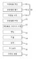
도 6은 본 발명의 일 실시예에 따른 액정디스플레이 장치의 벤딩 방법을 나타내는 순서도이고, 도 7은 본 발명의 일 실시예에 따른 벤딩 방법으로 제조된 액정디스플레이 장치를 도시한 결합단면도이다.6 is a flow chart showing a bending method of the liquid crystal display device according to an embodiment of the present invention, Figure 7 is a cross-sectional view showing a liquid crystal display device manufactured by the bending method according to an embodiment of the present invention.
도 6과 도 7을 참조하면, 본 발명의 일 실시예에 따른 액정디스플레이 장치의 벤딩 방법은 부착단계(S1)와, 벤딩단계(S3)와, 가열단계(S4)와, 냉각단계(S5)를 포함한다.6 and 7, a bending method of a liquid crystal display device according to an embodiment of the present invention includes an attaching step S1, a bending step S3, a heating step S4, and a cooling step S5. It includes.
부착단계(S1)는 상부기판(21)과 하부기판(23) 사이에 액정(25)이 주입되고 기설정된 두께를 갖는 액정셀(20)의 양면에 편광필름(30)을 결합한다.In the attaching step S1, the
액정셀(20)과 편광필름(30)의 결합 구조는 상술한 액정디스플레이 장치에 개시된 결합 구조를 이루도록 할 수 있다.The coupling structure of the
벤딩단계(S3)는 편광필름(30)이 결합된 액정셀(20)을 원하는 곡면 형태로 구부린다. 벤딩단계(S3)는 곡면 형태에 대응되는 지그(미도시)를 사용할 수 있다.In the bending step S3, the
벤딩단계(S3)에서 곡면 형태는 사용자가 원하는 형태로 구부릴 수 있다.In the bending step S3, the curved shape may be bent to a shape desired by the user.
가열단계(S4)는 편광필름(30)이 연화되도록 구부러진 액정셀(20)의 표면을 가열한다. 가열단계(S4)에서 액정셀(20)의 가열온도는 섭씨 60도 이상 섭씨 100도 이하를 이룬다.The heating step S4 heats the surface of the bent
액정셀(20)의 가열온도를 한정함으로써, 편광필름(30)의 연화가 용이하고, 편광필름(30)의 소성 변형을 방지할 수 있으며, 편광필름(30)의 편파가 변형되는 것을 방지할 수 있다.By limiting the heating temperature of the
여기서, 가열온도가 하한값보다 작은 경우, 편광필름(30)이 연화되지 않거나 편광필름(30)을 연화하는 데까지의 소요시간을 증가시켜 생산성이 저하될 수 있다.Here, when the heating temperature is less than the lower limit, productivity may be reduced by increasing the time required for the
또한, 가열온도가 상한값보다 큰 경우, 편광필름(30)을 연화하는 데까지의 소요시간을 제어하기 어렵고, 편광필름(30)이 소성 변형되어 편광필름(30)의 성질을 잃게 된다.In addition, when the heating temperature is greater than the upper limit, it is difficult to control the time required to soften the
가열단계(S4)는 편광필름(30)을 연화시키는 것이고, 액정셀(20)에서 상부기판(21)과 하부기판(23)은 연화되지 않는다.The heating step S4 is to soften the
벤딩단계(S3)와 가열단계(S4)의 순서는 여기서, 한정하지 않으나, 벤딩단계(S3)와 가열단계(S4)가 동시에 이루어지거나 벤딩단계(S3)와 가열단계(S4)가 순차적으로 이루어지는 것이 유리하다.The order of the bending step S3 and the heating step S4 is not limited thereto, but the bending step S3 and the heating step S4 are simultaneously performed or the bending step S3 and the heating step S4 are sequentially performed. It is advantageous.
가열단계(S4)가 벤딩단계(S3)보다 우선되는 경우, 연화된 편광필름(30)의 냉각을 방지하기 위한 별도의 수단이 필요할 수 있다.When the heating step S4 is prioritized over the bending step S3, a separate means for preventing cooling of the softened
냉각단계(S5)는 가열단계(S4)를 거쳐 연화된 편광필름(30)을 냉각시킨다.The cooling step S5 cools the softened
냉각단계는 가열단계(S4)를 정지시키고 자연대류에 의해 연화된 편광필름(30)을 냉각시킬 수 있다. 또한, 냉각단계(S5)는 가열단계(S4)를 정지시키고 냉기를 분사하여 연화된 편광필름(30)을 냉각시킬 수 있다.The cooling step may stop the heating step S4 and cool the
냉각단계(S5)를 거쳐 냉각된 편광필름(30)은 액정셀(20)의 곡면 형태와 동일한 형태를 유지하게 된다.The
이와 같이 액정셀(20)의 양면에 편광필름(30)이 부착된 상태에서 액정셀(20)을 원하는 곡면 형태로 구부리고, 편광필름(30)이 연화되도록 가열한 다음 냉각시킴으로써, 편광필름(30)이 액정셀(20)의 곡면 형태와 동일한 형태로 유지되고, 편광필름의 곡면 형태에 의해 액정셀(20)이 곡면 형태를 유지할 수 있다.As described above, the
본 발명의 일 실시예에 따른 액정디스플레이 장치의 벤딩 방법은 분리단계(S6)를 더 포함할 수 있다.Bending method of the liquid crystal display device according to an embodiment of the present invention may further include a separation step (S6).
분리단계(S6)는 벤딩단계(S3)에서 지그(미도시)를 사용하는 경우, 냉각단계(S5)를 거친 액정셀(20)에서 지그(미도시)를 분리한다. 분리단계(S6)를 거쳐 지그(미도시)가 분리되더라도 액정셀(20)은 냉각된 편광필름(30)에 의해 곡면 형태를 유지하게 된다.In the separating step S6, when a jig (not shown) is used in the bending step S3, the jig (not shown) is separated from the
본 발명의 일 실시예에 따른 액정디스플레이 장치의 벤딩 방법은 결합단계(S7)를 더 포함할 수 있다.Bending method of the liquid crystal display device according to an embodiment of the present invention may further comprise a bonding step (S7).
결합단계(S7)는 냉각단계(S5) 또는 분리단계(S6)를 거친 액정셀(20) 상측과 하측에 각각 기설정된 곡면 형태을 갖는 프레임부(50)가 결합된다.In the coupling step S7, the
결합단계(S7)를 거치면서 최종적으로 원하는 곡면 형태를 갖는 액정디스플레이 장치를 완성하게 된다.Through the coupling step (S7) to finally complete the liquid crystal display device having a desired curved shape.
이에 따라 상술한 액정디스플레이 장치는 도 7에 도시된 바와 같이 프레임부(50)를 더 포함할 수 있다. 프레임부(50)는 기설정된 곡면 형태를 가지고, 액정패널(10)의 양면에 각각 결합된다. 프레임부(50)는 액정패널(10)의 편광필름(30)에 각각 결합된다. 프레임부(50)는 액정패널(10)의 곡면 형태에 대응하여 기설정된 곡면 형태를 가질 수 있다.Accordingly, the above-described liquid crystal display device may further include a
여기서, 상술한 벤딩 방법을 통해 곡면 형태를 갖는 액정패널(10)의 곡률은 프레임부(50)의 곡률과 실질적으로 동일하게 형성되는 것이 바람직하지만, 액정패널(10)의 곡률은 프레임부(50)의 곡률보다 크거나 작을 수 있다.Here, although the curvature of the
여기서, 프레임부(50)에는 이탈방지부(51)가 형성될 수 있다.Here, the
이탈방지부(51)는 결합되는 액정패널(10)의 단부를 지지하도록 프레임부(50, 도 7참조)에 구비된다. 이탈방지부(51)는 결합되는 액정패널(10)의 곡면 형태에 대응되는 가상의 원에 대한 원주 방향으로 액정패널(10)이 유동되는 것을 억제 또는 방지한다.The
이탈방지부(51)는 프레임부(50)에서 연장 형성될 수 있다.The
한편, 이탈방지부(51)는 별도의 부재로 이루어져 프레임부(50)의 가장자리에 결합될 수 있다. 일예로, 이탈방지부(51)는 테이프로 이루어지고, 테이프 또는 프레임부(50)의 가장자리에 도포되는 접착제를 매개로 프레임부(50)의 가장자리에 결합될 수 있다.On the other hand, the
본 발명의 일 실시예에 따른 액정디스플레이 장치의 벤딩 방법은 박판제조단계(S0)를 더 포함할 수 있다.Bending method of the liquid crystal display device according to an embodiment of the present invention may further comprise a thin plate manufacturing step (S0).
박판제조단계(S0)는 부착단계(S1)에 앞서 액정셀(20)을 기설정된 두께로 감소시킨다.In the thin plate manufacturing step S0, the
박판제조단계(S0)는 액정셀(20)이 기설정된 두께를 갖도록 상부기판(21)의 표면과 하부기판(23)의 표면을 깎아낸다.In the thin plate manufacturing step S0, the surface of the
박판제조단계(S0)는 반입단계(S0-1)와, 식각단계(S0-3)를 포함할 수 있다.The thin plate manufacturing step S0 may include an import step S0-1 and an etching step S0-3.
반입단계(S0-1)는 액정셀(20)을 반입한다. 식각단계(S0-3)는 액정셀(20)이 기설정된 두께로 감소되도록 상부기판(21)의 표면과 하부기판(23)의 표면을 각각 깎아낸다.In the import step S0-1, the
식각단계(S0-3)는 상부기판(21)의 표면 전체와 하부기판(23)의 표면 전체를 각각 깎아낼 수 있다. 한편, 식각단계(S0-3)는 상부기판(21)의 가장자리와 하부기판(23)의 가장자리를 제외한 상부기판(21)의 표면과 하부기판(23)의 표면을 각각 깎아낼 수 있다.In the etching step S0-3, the entire surface of the
박판제조단계(S0)는 제거단계(S0-2)를 더 포함할 수 있다. 제거단계(S0-2)는 반입단계(S0-1)에서 반입되는 액정셀(20)에 편광필름(30)이 결합된 경우, 반입단계(S0-1)를 거쳐 반입되는 액정셀(20)에서 편광필름(30)을 제거한다.The thin plate manufacturing step S0 may further include a removing step S0-2. In the removing step S0-2, when the
이에 따라 반입되는 액정셀(20)을 기설정된 두께를 갖는 초박형 액정셀(20)으로 가공할 수 있다.Accordingly, the
본 발명의 일 실시예에 따른 액정디스플레이 장치의 벤딩 방법은 마감단계(S2)를 더 포함할 수 있다.Bending method of the liquid crystal display device according to an embodiment of the present invention may further include a finishing step (S2).
마감단계(S2)는 부착단계(S1)를 거쳐 편광필름(30)이 결합된 액정셀(20)의 가장자리를 감싼다. 마감단계(S2)를 거치면서 편광필름(30)이 결합된 액정셀(20)의 가장자리에는 마감부(40)가 형성될 수 있다.The finishing step S2 surrounds the edge of the
상술한 액정디스플레이 장치와, 액정디스플레이 장치의 벤딩 방법에 따르면, 초박형으로 구성되거나 원하는 곡면 형태로 구부러진 액정셀(20)에 휨응력, 진동, 충격 등과 같은 외력이 가해질 때, 액정셀(20)이 파손되는 것을 방지할 수 있다.
According to the above-described liquid crystal display device and the bending method of the liquid crystal display device, when the external force such as bending stress, vibration, impact, etc. is applied to the
본 발명은 도면에 도시된 실시예를 참고로 하여 설명되었으나, 이는 예시적인 것에 불과하며, 당해 기술이 속하는 분야에서 통상의 지식을 가진 자라면 이로부터 다양한 변형 및 균등한 타 실시예가 가능하다는 점을 이해할 것이다.While the present invention has been particularly shown and described with reference to exemplary embodiments thereof, it will be understood by those of ordinary skill in the art that various changes in form and details may be made therein without departing from the spirit and scope of the invention as defined by the appended claims. I will understand.
따라서, 본 발명의 진정한 기술적 보호범위는 특허청구범위에 의해서 정하여져야 할 것이다.
Accordingly, the true scope of protection of the present invention should be defined by the claims.
10: 액정패널20: 액정셀
21: 상부기판23: 하부기판
25: 액정30: 편광필름
31: 제1편광필름32: 제2편광필름
40: 마감부41: 필름연장부
43: 몰딩부50: 프레임부
51: 이탈방지부S0: 박판제조단계
S0-1: 반입단계S0-2: 제거단계
S0-3: 식각단계S1: 부착단계
S2: 마감단계S3: 벤딩단계
S4: 가열단계S5: 냉각단계
S6: 분리단계S7: 결합단계10: liquid crystal panel 20: liquid crystal cell
21: upper substrate 23: lower substrate
25: liquid crystal 30: polarizing film
31: first polarizing film 32: second polarizing film
40: finish portion 41: film extension portion
43: molding part 50: frame part
51: departure prevention part S0: sheet manufacturing step
S0-1: Import step S0-2: Remove step
S0-3: Etching Step S1: Attaching Step
S2: Finishing Step S3: Bending Step
S4: heating step S5: cooling step
S6: Separation step S7: Joining step
Claims (9)
Translated fromKorean상기 부착단계를 거친 상기 액정패널을 곡면 형태로 구부리는 벤딩단계;
상기 편광필름이 연화되도록 상기 액정패널의 표면을 가열하는 가열단계; 및
상기 가열단계를 거쳐 연화된 상기 편광필름을 냉각시키는 냉각단계; 를 포함하고,
상기 냉각단계를 거친 상기 액정패널의 양면에 각각 프레임부를 결합하는 결합단계; 를 더 포함하며,
상기 프레임부에는,
상기 액정패널의 단부를 지지하는 이탈방지부; 가 구비되는 것을 특징으로 하는 액정디스플레이 장치의 벤딩 방법.
An attaching step of forming a liquid crystal panel by injecting a liquid crystal between the upper substrate and the lower substrate and combining a polarizing film on both sides of the liquid crystal cell having a predetermined thickness;
Bending the liquid crystal panel that has undergone the attaching step into a curved shape;
A heating step of heating the surface of the liquid crystal panel to soften the polarizing film; And
A cooling step of cooling the polarizing film softened through the heating step; Lt; / RTI >
Combining the frame parts on both sides of the liquid crystal panel after the cooling step; Further comprising:
In the frame portion,
A separation prevention part supporting an end of the liquid crystal panel; Bending method of the liquid crystal display device characterized in that the provided.
상기 벤딩단계에서 상기 곡면 형태에 대응되는 지그를 사용하는 경우,
상기 냉각단계를 거친 상기 액정패널에서 상기 지그를 분리하는 분리단계; 를 더 포함하는 것을 특징으로 하는 액정디스플레이 장치의 벤딩 방법.
The method of claim 1,
When using the jig corresponding to the curved shape in the bending step,
A separation step of separating the jig from the liquid crystal panel through the cooling step; Bending method of the liquid crystal display device characterized in that it further comprises.
상기 부착단계를 거쳐 상기 액정셀에 결합된 상기 편광필름의 두께는, 상기 액정셀의 두께와 같거나 크게 형성되는 것을 특징으로 하는 액정디스플레이 장치의 벤딩 방법.
The method of claim 1,
The thickness of the polarizing film coupled to the liquid crystal cell through the attachment step, the bending method of the liquid crystal display device, characterized in that the same or larger than the thickness of the liquid crystal cell.
상기 부착단계에 앞서 상기 액정셀을 기설정된 두께로 감소시키는 박판제조단계; 를 더 포함하는 것을 특징으로 하는 액정디스플레이 장치의 벤딩 방법.
The method according to any one of claims 1, 2, and 5,
A thin plate manufacturing step of reducing the liquid crystal cell to a predetermined thickness prior to the attaching step; Bending method of the liquid crystal display device characterized in that it further comprises.
상기 박판제조단계는,
상기 액정셀을 반입하는 반입단계; 및
상기 액정셀이 기설정된 두께로 감소되도록 상기 상부기판과 상기 하부기판을 각각 깎아내는 식각단계; 를 포함하는 것을 특징으로 하는 액정디스플레이 장치의 벤딩 방법.
The method according to claim 6,
The sheet manufacturing step,
An import step of bringing in the liquid crystal cell; And
An etching step of cutting the upper substrate and the lower substrate to reduce the liquid crystal cell to a predetermined thickness; Bending method of the liquid crystal display device comprising a.
상기 박판제조단계는,
상기 반입단계를 거친 상기 액정셀에 상기 편광필름이 결합된 경우,
상기 반입단계를 거쳐 반입된 상기 액정셀에서 상기 편광필름을 제거하는 제거단계; 를 더 포함하는 것을 특징으로 하는 액정디스플레이 장치의 벤딩 방법.
8. The method of claim 7,
The sheet manufacturing step,
When the polarizing film is coupled to the liquid crystal cell passed through the import step,
A removing step of removing the polarizing film from the liquid crystal cell brought in through the loading step; Bending method of the liquid crystal display device characterized in that it further comprises.
상기 부착단계를 거친 상기 액정패널의 가장자리를 감싸는 마감단계; 가 더 포함되는 것을 특징으로 하는 액정디스플레이 장치의 벤딩 방법.
The method according to any one of claims 1, 2, and 5,
A finishing step of wrapping an edge of the liquid crystal panel through the attaching step; Bending method of the liquid crystal display device characterized in that it further comprises.
Priority Applications (1)
| Application Number | Priority Date | Filing Date | Title |
|---|---|---|---|
| KR1020120097893AKR101381610B1 (en) | 2012-09-04 | 2012-09-04 | Bending method of liquid crystal display device |
Applications Claiming Priority (1)
| Application Number | Priority Date | Filing Date | Title |
|---|---|---|---|
| KR1020120097893AKR101381610B1 (en) | 2012-09-04 | 2012-09-04 | Bending method of liquid crystal display device |
Publications (2)
| Publication Number | Publication Date |
|---|---|
| KR20140031020A KR20140031020A (en) | 2014-03-12 |
| KR101381610B1true KR101381610B1 (en) | 2014-04-04 |
Family
ID=50643339
Family Applications (1)
| Application Number | Title | Priority Date | Filing Date |
|---|---|---|---|
| KR1020120097893AActiveKR101381610B1 (en) | 2012-09-04 | 2012-09-04 | Bending method of liquid crystal display device |
Country Status (1)
| Country | Link |
|---|---|
| KR (1) | KR101381610B1 (en) |
Cited By (63)
| Publication number | Priority date | Publication date | Assignee | Title |
|---|---|---|---|---|
| CN105589246A (en)* | 2014-11-11 | 2016-05-18 | 三星显示有限公司 | Curved display device |
| USD812147S1 (en) | 2016-03-30 | 2018-03-06 | Bally Gaming, Inc. | Gaming machine with curved display |
| USD832358S1 (en) | 2016-09-13 | 2018-10-30 | Bally Gaming, Inc. | Gaming machine with curved display |
| USD832355S1 (en) | 2016-09-13 | 2018-10-30 | Bally Gaming, Inc. | Gaming machine with curved display |
| USD832356S1 (en) | 2016-09-13 | 2018-10-30 | Bally Gaming, Inc. | Gaming machine with curved display |
| USD832357S1 (en) | 2016-09-13 | 2018-10-30 | Bally Gaming, Inc. | Gaming machine with curved display |
| USD836164S1 (en) | 2016-09-13 | 2018-12-18 | Bally Gaming, Inc. | Curved display for a gaming machine |
| USD843460S1 (en) | 2016-09-13 | 2019-03-19 | Bally Gaming, Inc. | Gaming machine with curved display |
| USD843463S1 (en) | 2016-09-13 | 2019-03-19 | Bally Gaming, Inc. | Gaming machine with curved display |
| USD843458S1 (en) | 2016-03-30 | 2019-03-19 | Bally Gaming, Inc. | Gaming machine with curved display |
| USD843464S1 (en) | 2016-09-13 | 2019-03-19 | Bally Gaming, Inc. | Gaming machine with curved display |
| USD843478S1 (en) | 2013-04-17 | 2019-03-19 | Bally Gaming, Inc. | Gaming machine |
| USD843465S1 (en) | 2016-09-13 | 2019-03-19 | Bally Gaming, Inc. | Gaming machine with curved display |
| USD843466S1 (en) | 2016-09-13 | 2019-03-19 | Bally Gaming, Inc. | Gaming machine with curved display |
| USD843459S1 (en) | 2016-03-30 | 2019-03-19 | Bally Gaming, Inc. | Gaming machine with curved display |
| USD843480S1 (en) | 2018-06-01 | 2019-03-19 | Bally Gaming, Inc. | Gaming machine with curved display |
| USD843461S1 (en) | 2016-09-13 | 2019-03-19 | Bally Gaming, Inc. | Gaming machine with curved display |
| USD843462S1 (en) | 2016-09-13 | 2019-03-19 | Bally Gaming, Inc. | Gaming machine with curved display |
| USD843477S1 (en) | 2013-04-17 | 2019-03-19 | Bally Gaming, Inc. | Gaming machine |
| USD850537S1 (en) | 2017-09-05 | 2019-06-04 | Aristocrat Technologies Australia Pty Limited | Gaming machine |
| USD871506S1 (en) | 2016-09-13 | 2019-12-31 | Bally Gaming, Inc. | Gaming machine with curved displays |
| USD872189S1 (en) | 2018-07-24 | 2020-01-07 | Bally Gaming, Inc. | Gaming machine |
| USD872188S1 (en) | 2018-07-24 | 2020-01-07 | Bally Gaming, Inc. | Gaming machine |
| USD873921S1 (en) | 2018-07-24 | 2020-01-28 | Bally Gaming, Inc. | Gaming machine |
| USD877811S1 (en) | 2018-07-02 | 2020-03-10 | Sg Gaming, Inc. | Gaming machine |
| USD878477S1 (en) | 2018-07-02 | 2020-03-17 | Sg Gaming, Inc. | Gaming machine |
| USD880614S1 (en) | 2018-07-24 | 2020-04-07 | Sg Gaming, Inc. | Gaming machine |
| USD880610S1 (en) | 2018-07-24 | 2020-04-07 | Sg Gaming, Inc. | Gaming machine |
| USD880608S1 (en) | 2018-07-24 | 2020-04-07 | Sg Gaming, Inc. | Gaming machine |
| USD880612S1 (en) | 2018-07-24 | 2020-04-07 | Sg Gaming, Inc. | Gaming machine |
| USD880606S1 (en) | 2017-09-28 | 2020-04-07 | Sg Gaming, Inc. | Gaming terminal |
| USD880613S1 (en) | 2018-07-24 | 2020-04-07 | Sg Gaming, Inc. | Gaming machine |
| USD880609S1 (en) | 2018-07-24 | 2020-04-07 | Bally Gaming, Inc. | Gaming machine with graphical user interface |
| USD880611S1 (en) | 2018-07-24 | 2020-04-07 | Sg Gaming, Inc. | Gaming machine |
| USD880615S1 (en) | 2018-07-24 | 2020-04-07 | Sg Gaming, Inc. | Gaming machine |
| USD881284S1 (en) | 2018-07-24 | 2020-04-14 | Sg Gaming, Inc. | Gaming machine |
| USD881285S1 (en) | 2018-07-24 | 2020-04-14 | Sg Gaming, Inc. | Gaming machine |
| USD881995S1 (en) | 2018-07-24 | 2020-04-21 | Sg Gaming, Inc. | Gaming machine |
| USD882694S1 (en) | 2018-07-24 | 2020-04-28 | Sg Gaming, Inc. | Gaming machine |
| USD882699S1 (en) | 2017-04-14 | 2020-04-28 | Sg Gaming, Inc. | Gaming machine carousel display |
| USD882695S1 (en) | 2018-07-24 | 2020-04-28 | Sg Gaming, Inc. | Gaming machine |
| USD882700S1 (en) | 2017-04-14 | 2020-04-28 | Sg Gaming, Inc. | Gaming machine carousel display |
| USD883393S1 (en) | 2017-04-14 | 2020-05-05 | Sg Gaming, Inc. | Gaming machine carousel display |
| USD884079S1 (en) | 2018-07-24 | 2020-05-12 | Sg Gaming, Inc. | Gaming machine |
| USD886905S1 (en) | 2018-07-24 | 2020-06-09 | Sg Gaming, Inc. | Gaming machine |
| USD887495S1 (en) | 2018-07-24 | 2020-06-16 | Sg Gaming, Inc. | Gaming machine |
| USD889552S1 (en) | 2017-09-28 | 2020-07-07 | Sg Gaming, Inc. | Gaming terminal |
| USD889553S1 (en) | 2017-09-28 | 2020-07-07 | Sg Gaming, Inc. | Gaming terminal |
| USD894285S1 (en) | 2018-07-24 | 2020-08-25 | Sg Gaming, Inc. | Gaming machine |
| USD896313S1 (en) | 2016-03-30 | 2020-09-15 | Sg Gaming, Inc. | Gaming machine with curved display |
| USD913376S1 (en) | 2018-07-02 | 2021-03-16 | Sg Gaming, Inc. | Gaming machine |
| USD913377S1 (en) | 2018-07-02 | 2021-03-16 | Sg Gaming, Inc. | Gaming machine |
| USD915523S1 (en) | 2017-09-28 | 2021-04-06 | Sg Gaming, Inc. | Gaming terminal |
| USD952753S1 (en) | 2019-10-11 | 2022-05-24 | Sg Gaming, Inc. | Gaming machine |
| USD952752S1 (en) | 2019-10-11 | 2022-05-24 | Sg Gaming, Inc. | Gaming machine |
| USD952750S1 (en) | 2019-10-11 | 2022-05-24 | Sg Gaming, Inc. | Gaming machine |
| USD952751S1 (en) | 2019-10-11 | 2022-05-24 | Sg Gaming, Inc. | Gaming machine |
| USD952754S1 (en) | 2019-10-11 | 2022-05-24 | Sg Gaming, Inc. | Gaming machine |
| USD952755S1 (en) | 2019-10-11 | 2022-05-24 | Sg Gaming, Inc. | Gaming machine |
| US11854345B2 (en) | 2019-08-30 | 2023-12-26 | Aristocrat Technologies Australia Pty Limited | Systems and methods for supplementing a wagering game |
| USD1023156S1 (en) | 2019-08-29 | 2024-04-16 | Aristocrat Technologies Australia Pty Limited | Gaming machine with stepper reel and display screen with a transitional graphical user interface |
| USD1034821S1 (en) | 2018-07-24 | 2024-07-09 | Lnw Gaming, Inc. | Gaming machine |
| USD1034820S1 (en) | 2018-07-24 | 2024-07-09 | Lnw Gaming, Inc. | Gaming machine |
Families Citing this family (1)
| Publication number | Priority date | Publication date | Assignee | Title |
|---|---|---|---|---|
| WO2019208918A1 (en)* | 2018-04-26 | 2019-10-31 | (주)코텍 | Liquid crystal panel and method for etching liquid crystal panel |
Citations (4)
| Publication number | Priority date | Publication date | Assignee | Title |
|---|---|---|---|---|
| JPH10268790A (en)* | 1997-03-24 | 1998-10-09 | Seiko Epson Corp | LIQUID CRYSTAL DISPLAY PANEL HOLDER, LIQUID CRYSTAL DISPLAY USING THE SAME, ELECTRONIC APPARATUS USING THE LIQUID CRYSTAL DISPLAY DEVICE, CURABLE LIQUID CRYSTAL DISPLAY PANEL MANUFACTURING JIG AND METHOD FOR MANUFACTURING CURVED LIQUID CRYSTAL DISPLAY PANEL USING THE SAME |
| JP2005250097A (en)* | 2004-03-04 | 2005-09-15 | Nitto Denko Corp | Optical member, manufacturing method thereof, and image display device |
| JP2010066462A (en)* | 2008-09-10 | 2010-03-25 | Mitsubishi Electric Corp | Liquid crystal panel and method of manufacturing the same |
| JP2010224102A (en)* | 2009-03-23 | 2010-10-07 | Hitachi Displays Ltd | Liquid crystal display device and manufacturing method thereof |
- 2012
- 2012-09-04KRKR1020120097893Apatent/KR101381610B1/enactiveActive
Patent Citations (4)
| Publication number | Priority date | Publication date | Assignee | Title |
|---|---|---|---|---|
| JPH10268790A (en)* | 1997-03-24 | 1998-10-09 | Seiko Epson Corp | LIQUID CRYSTAL DISPLAY PANEL HOLDER, LIQUID CRYSTAL DISPLAY USING THE SAME, ELECTRONIC APPARATUS USING THE LIQUID CRYSTAL DISPLAY DEVICE, CURABLE LIQUID CRYSTAL DISPLAY PANEL MANUFACTURING JIG AND METHOD FOR MANUFACTURING CURVED LIQUID CRYSTAL DISPLAY PANEL USING THE SAME |
| JP2005250097A (en)* | 2004-03-04 | 2005-09-15 | Nitto Denko Corp | Optical member, manufacturing method thereof, and image display device |
| JP2010066462A (en)* | 2008-09-10 | 2010-03-25 | Mitsubishi Electric Corp | Liquid crystal panel and method of manufacturing the same |
| JP2010224102A (en)* | 2009-03-23 | 2010-10-07 | Hitachi Displays Ltd | Liquid crystal display device and manufacturing method thereof |
Cited By (109)
| Publication number | Priority date | Publication date | Assignee | Title |
|---|---|---|---|---|
| USD882696S1 (en) | 2013-04-17 | 2020-04-28 | Sg Gaming, Inc. | Gaming machine |
| USD882698S1 (en) | 2013-04-17 | 2020-04-28 | Sg Gaming, Inc. | Gaming machine |
| USD843476S1 (en) | 2013-04-17 | 2019-03-19 | Bally Gaming, Inc. | Gaming machine |
| USD843477S1 (en) | 2013-04-17 | 2019-03-19 | Bally Gaming, Inc. | Gaming machine |
| USD843475S1 (en) | 2013-04-17 | 2019-03-19 | Bally Gaming, Inc. | Gaming machine |
| USD844062S1 (en) | 2013-04-17 | 2019-03-26 | Bally Gaming, Inc. | Gaming machine |
| USD882697S1 (en) | 2013-04-17 | 2020-04-28 | Sg Gaming, Inc. | Gaming machine |
| USD843478S1 (en) | 2013-04-17 | 2019-03-19 | Bally Gaming, Inc. | Gaming machine |
| USD895019S1 (en) | 2013-04-17 | 2020-09-01 | Sg Gaming, Inc. | Gaming machine |
| USD843474S1 (en) | 2013-04-17 | 2019-03-19 | Bally Gaming, Inc. | Gaming machine |
| CN105589246A (en)* | 2014-11-11 | 2016-05-18 | 三星显示有限公司 | Curved display device |
| USD896315S1 (en) | 2016-03-30 | 2020-09-15 | Sg Gaming, Inc. | Gaming machine with curved display |
| USD812147S1 (en) | 2016-03-30 | 2018-03-06 | Bally Gaming, Inc. | Gaming machine with curved display |
| USD896313S1 (en) | 2016-03-30 | 2020-09-15 | Sg Gaming, Inc. | Gaming machine with curved display |
| USD843458S1 (en) | 2016-03-30 | 2019-03-19 | Bally Gaming, Inc. | Gaming machine with curved display |
| USD896312S1 (en) | 2016-03-30 | 2020-09-15 | Sg Gaming, Inc. | Gaming machine with curved display |
| USD843479S1 (en) | 2016-03-30 | 2019-03-19 | Bally Gaming, Inc. | Gaming machine with curved display |
| USD910116S1 (en) | 2016-03-30 | 2021-02-09 | Sg Gaming, Inc. | Gaming machine with curved display |
| USD896314S1 (en) | 2016-03-30 | 2020-09-15 | Sg Gaming, Inc. | Gaming machine with curved display |
| USD843459S1 (en) | 2016-03-30 | 2019-03-19 | Bally Gaming, Inc. | Gaming machine with curved display |
| USD1055165S1 (en) | 2016-03-30 | 2024-12-24 | Lnw Gaming, Inc. | Gaming machine with curved display |
| USD819747S1 (en) | 2016-03-30 | 2018-06-05 | Bally Gaming, Inc. | Gaming machine with curved display |
| USD812146S1 (en) | 2016-03-30 | 2018-03-06 | Bally Gaming, Inc. | Gaming machine with curved display |
| USD812148S1 (en) | 2016-03-30 | 2018-03-06 | Bally Gaming, Inc. | Gaming machine with curved display |
| USD812149S1 (en) | 2016-03-30 | 2018-03-06 | Bally Gaming, Inc. | Gaming machine with curved display |
| USD843460S1 (en) | 2016-09-13 | 2019-03-19 | Bally Gaming, Inc. | Gaming machine with curved display |
| USD836164S1 (en) | 2016-09-13 | 2018-12-18 | Bally Gaming, Inc. | Curved display for a gaming machine |
| USD843461S1 (en) | 2016-09-13 | 2019-03-19 | Bally Gaming, Inc. | Gaming machine with curved display |
| USD843466S1 (en) | 2016-09-13 | 2019-03-19 | Bally Gaming, Inc. | Gaming machine with curved display |
| USD832358S1 (en) | 2016-09-13 | 2018-10-30 | Bally Gaming, Inc. | Gaming machine with curved display |
| USD871506S1 (en) | 2016-09-13 | 2019-12-31 | Bally Gaming, Inc. | Gaming machine with curved displays |
| USD843465S1 (en) | 2016-09-13 | 2019-03-19 | Bally Gaming, Inc. | Gaming machine with curved display |
| USD843464S1 (en) | 2016-09-13 | 2019-03-19 | Bally Gaming, Inc. | Gaming machine with curved display |
| USD832355S1 (en) | 2016-09-13 | 2018-10-30 | Bally Gaming, Inc. | Gaming machine with curved display |
| USD843463S1 (en) | 2016-09-13 | 2019-03-19 | Bally Gaming, Inc. | Gaming machine with curved display |
| USD843462S1 (en) | 2016-09-13 | 2019-03-19 | Bally Gaming, Inc. | Gaming machine with curved display |
| USD832357S1 (en) | 2016-09-13 | 2018-10-30 | Bally Gaming, Inc. | Gaming machine with curved display |
| USD832356S1 (en) | 2016-09-13 | 2018-10-30 | Bally Gaming, Inc. | Gaming machine with curved display |
| USD883393S1 (en) | 2017-04-14 | 2020-05-05 | Sg Gaming, Inc. | Gaming machine carousel display |
| USD882700S1 (en) | 2017-04-14 | 2020-04-28 | Sg Gaming, Inc. | Gaming machine carousel display |
| USD882699S1 (en) | 2017-04-14 | 2020-04-28 | Sg Gaming, Inc. | Gaming machine carousel display |
| USD850537S1 (en) | 2017-09-05 | 2019-06-04 | Aristocrat Technologies Australia Pty Limited | Gaming machine |
| USD870820S1 (en) | 2017-09-05 | 2019-12-24 | Aristocrat Technologies Australia Pty Limited | Gaming machine display |
| USD898128S1 (en) | 2017-09-05 | 2020-10-06 | Aristocrat Technologies Australia Pty Limited | Gaming machine |
| USD1042647S1 (en) | 2017-09-05 | 2024-09-17 | Aristocrat Technologies Australia Pty Limited | Gaming machine |
| USD1040237S1 (en) | 2017-09-05 | 2024-08-27 | Aristocrat Technologies Australia Pty Limited | Gaming machine |
| USD1040238S1 (en) | 2017-09-05 | 2024-08-27 | Aristocrat Technologies Australia Pty Limited | Gaming machine |
| USD871507S1 (en) | 2017-09-05 | 2019-12-31 | Aristocrat Technologies Australia Pty Limited | Gaming machine display |
| USD1031855S1 (en) | 2017-09-28 | 2024-06-18 | Lnw Gaming, Inc. | Gaming terminal |
| USD889552S1 (en) | 2017-09-28 | 2020-07-07 | Sg Gaming, Inc. | Gaming terminal |
| USD1031854S1 (en) | 2017-09-28 | 2024-06-18 | Lnw Gaming, Inc. | Gaming terminal |
| USD1031853S1 (en) | 2017-09-28 | 2024-06-18 | Lnw Gaming, Inc. | Gaming terminal |
| USD880606S1 (en) | 2017-09-28 | 2020-04-07 | Sg Gaming, Inc. | Gaming terminal |
| USD1032728S1 (en) | 2017-09-28 | 2024-06-25 | Lnw Gaming, Inc. | Gaming terminal |
| USD1002738S1 (en) | 2017-09-28 | 2023-10-24 | Lnw Gaming, Inc. | Gaming terminal |
| USD1031852S1 (en) | 2017-09-28 | 2024-06-18 | Lnw Gaming, Inc. | Gaming terminal |
| USD915523S1 (en) | 2017-09-28 | 2021-04-06 | Sg Gaming, Inc. | Gaming terminal |
| USD889553S1 (en) | 2017-09-28 | 2020-07-07 | Sg Gaming, Inc. | Gaming terminal |
| USD1036553S1 (en) | 2017-09-28 | 2024-07-23 | Lnw Gaming, Inc. | Gaming terminal |
| USD843480S1 (en) | 2018-06-01 | 2019-03-19 | Bally Gaming, Inc. | Gaming machine with curved display |
| USD877811S1 (en) | 2018-07-02 | 2020-03-10 | Sg Gaming, Inc. | Gaming machine |
| USD913376S1 (en) | 2018-07-02 | 2021-03-16 | Sg Gaming, Inc. | Gaming machine |
| USD913377S1 (en) | 2018-07-02 | 2021-03-16 | Sg Gaming, Inc. | Gaming machine |
| USD878477S1 (en) | 2018-07-02 | 2020-03-17 | Sg Gaming, Inc. | Gaming machine |
| USD1018678S1 (en) | 2018-07-24 | 2024-03-19 | Lnw Gaming, Inc. | Gaming machine |
| USD1034821S1 (en) | 2018-07-24 | 2024-07-09 | Lnw Gaming, Inc. | Gaming machine |
| USD872188S1 (en) | 2018-07-24 | 2020-01-07 | Bally Gaming, Inc. | Gaming machine |
| USD872189S1 (en) | 2018-07-24 | 2020-01-07 | Bally Gaming, Inc. | Gaming machine |
| USD894285S1 (en) | 2018-07-24 | 2020-08-25 | Sg Gaming, Inc. | Gaming machine |
| USD887495S1 (en) | 2018-07-24 | 2020-06-16 | Sg Gaming, Inc. | Gaming machine |
| USD886905S1 (en) | 2018-07-24 | 2020-06-09 | Sg Gaming, Inc. | Gaming machine |
| USD884079S1 (en) | 2018-07-24 | 2020-05-12 | Sg Gaming, Inc. | Gaming machine |
| USD880614S1 (en) | 2018-07-24 | 2020-04-07 | Sg Gaming, Inc. | Gaming machine |
| USD1069922S1 (en) | 2018-07-24 | 2025-04-08 | Lnw Gaming, Inc. | Gaming machine |
| USD1068941S1 (en) | 2018-07-24 | 2025-04-01 | Lnw Gaming, Inc. | Gaming machine with graphical user interface |
| USD880609S1 (en) | 2018-07-24 | 2020-04-07 | Bally Gaming, Inc. | Gaming machine with graphical user interface |
| USD880611S1 (en) | 2018-07-24 | 2020-04-07 | Sg Gaming, Inc. | Gaming machine |
| USD880615S1 (en) | 2018-07-24 | 2020-04-07 | Sg Gaming, Inc. | Gaming machine |
| USD881284S1 (en) | 2018-07-24 | 2020-04-14 | Sg Gaming, Inc. | Gaming machine |
| USD880610S1 (en) | 2018-07-24 | 2020-04-07 | Sg Gaming, Inc. | Gaming machine |
| USD881285S1 (en) | 2018-07-24 | 2020-04-14 | Sg Gaming, Inc. | Gaming machine |
| USD1011431S1 (en) | 2018-07-24 | 2024-01-16 | Lnw Gaming, Inc. | Gaming machine |
| USD1011430S1 (en) | 2018-07-24 | 2024-01-16 | Lnw Gaming, Inc. | Gaming machine |
| USD1012185S1 (en) | 2018-07-24 | 2024-01-23 | Lnw Gaming, Inc. | Gaming machine |
| USD1012184S1 (en) | 2018-07-24 | 2024-01-23 | Lnw Gaming, Inc. | Gaming machine with graphical user interface |
| USD1012183S1 (en) | 2018-07-24 | 2024-01-23 | Lnw Gaming, Inc. | Gaming machine |
| USD1012186S1 (en) | 2018-07-24 | 2024-01-23 | Lnw Gaming, Inc. | Gaming machine with graphical user interface |
| USD1013044S1 (en) | 2018-07-24 | 2024-01-30 | Lnw Gaming, Inc. | Gaming machine |
| USD1018677S1 (en) | 2018-07-24 | 2024-03-19 | Lnw Gaming, Inc. | Gaming machine |
| USD880613S1 (en) | 2018-07-24 | 2020-04-07 | Sg Gaming, Inc. | Gaming machine |
| USD1034820S1 (en) | 2018-07-24 | 2024-07-09 | Lnw Gaming, Inc. | Gaming machine |
| USD880608S1 (en) | 2018-07-24 | 2020-04-07 | Sg Gaming, Inc. | Gaming machine |
| USD882695S1 (en) | 2018-07-24 | 2020-04-28 | Sg Gaming, Inc. | Gaming machine |
| USD880612S1 (en) | 2018-07-24 | 2020-04-07 | Sg Gaming, Inc. | Gaming machine |
| USD882694S1 (en) | 2018-07-24 | 2020-04-28 | Sg Gaming, Inc. | Gaming machine |
| USD1032721S1 (en) | 2018-07-24 | 2024-06-25 | Lnw Gaming, Inc. | Gaming machine with graphical user interface |
| USD881995S1 (en) | 2018-07-24 | 2020-04-21 | Sg Gaming, Inc. | Gaming machine |
| USD1033542S1 (en) | 2018-07-24 | 2024-07-02 | Lnw Gaming, Inc. | Gaming machine |
| USD873921S1 (en) | 2018-07-24 | 2020-01-28 | Bally Gaming, Inc. | Gaming machine |
| USD1023156S1 (en) | 2019-08-29 | 2024-04-16 | Aristocrat Technologies Australia Pty Limited | Gaming machine with stepper reel and display screen with a transitional graphical user interface |
| USD1046978S1 (en) | 2019-08-29 | 2024-10-15 | Aristocrat Technologies Australia Pty Limited | Gaming machine with stepper reel and display screen with a transitional graphical user interface |
| US11854345B2 (en) | 2019-08-30 | 2023-12-26 | Aristocrat Technologies Australia Pty Limited | Systems and methods for supplementing a wagering game |
| US12249216B2 (en) | 2019-08-30 | 2025-03-11 | Aristocrat Technologies Australia Pty Limited | Systems and methods for supplementing a wagering game |
| USD952755S1 (en) | 2019-10-11 | 2022-05-24 | Sg Gaming, Inc. | Gaming machine |
| USD952754S1 (en) | 2019-10-11 | 2022-05-24 | Sg Gaming, Inc. | Gaming machine |
| USD952751S1 (en) | 2019-10-11 | 2022-05-24 | Sg Gaming, Inc. | Gaming machine |
| USD952750S1 (en) | 2019-10-11 | 2022-05-24 | Sg Gaming, Inc. | Gaming machine |
| USD952752S1 (en) | 2019-10-11 | 2022-05-24 | Sg Gaming, Inc. | Gaming machine |
| USD952753S1 (en) | 2019-10-11 | 2022-05-24 | Sg Gaming, Inc. | Gaming machine |
Also Published As
| Publication number | Publication date |
|---|---|
| KR20140031020A (en) | 2014-03-12 |
Similar Documents
| Publication | Publication Date | Title |
|---|---|---|
| KR101381610B1 (en) | Bending method of liquid crystal display device | |
| KR101381609B1 (en) | Liquid crystal display device and bending method of this | |
| KR101336677B1 (en) | Liquid crystal display device and bending method of this | |
| US9784998B2 (en) | Method for manufacturing curved display | |
| KR101539221B1 (en) | Curved Shape Display Module and Manufacturing Method thereof | |
| US20060098185A1 (en) | Mask holder for irradiating UV-rays | |
| US20110025940A1 (en) | Display panel and method for narrowing edges and increasing edge strength thereof | |
| CN102722049B (en) | Polaroid splicing method | |
| JP2007516461A (en) | Glass products for use in ultra-thin glass display applications | |
| WO2016044360A1 (en) | Curved liquid crystal display panel and process of manufacture | |
| AU2012305176A1 (en) | Method for manufacturing curved-surface display | |
| CN101341437A (en) | Liquid crystal display device and mobile communication terminal having the liquid crystal display device | |
| JP2006106079A (en) | Electro-optical device, electronic apparatus using the same, and method of manufacturing electro-optical device | |
| WO2016163281A1 (en) | Liquid crystal display device and method for manufacturing liquid crystal display device | |
| CN108885363A (en) | Manufacturing method of liquid crystal panel | |
| US10809563B2 (en) | Liquid crystal display device | |
| US9256093B2 (en) | Display apparatus and method for manufacturing the same | |
| KR20150142521A (en) | Curved display device | |
| CN105044997A (en) | Liquid crystal display panel, a preparation method thereof and liquid crystal display device | |
| US9268161B2 (en) | Method for manufacturing a liquid crystal panel | |
| KR101872242B1 (en) | Curved type display and manufacturing method thereof | |
| KR20070060810A (en) | Manufacturing method of liquid crystal display panel | |
| US8894797B2 (en) | Method of splicing polarized films | |
| JP2017016015A (en) | Liquid crystal display | |
| KR102494150B1 (en) | Liquid crystal display device |
Legal Events
| Date | Code | Title | Description |
|---|---|---|---|
| A201 | Request for examination | ||
| PA0109 | Patent application | Patent event code:PA01091R01D Comment text:Patent Application Patent event date:20120904 | |
| PA0201 | Request for examination | ||
| E902 | Notification of reason for refusal | ||
| PE0902 | Notice of grounds for rejection | Comment text:Notification of reason for refusal Patent event date:20130924 Patent event code:PE09021S01D | |
| PG1501 | Laying open of application | ||
| E701 | Decision to grant or registration of patent right | ||
| PE0701 | Decision of registration | Patent event code:PE07011S01D Comment text:Decision to Grant Registration Patent event date:20140320 | |
| PR0701 | Registration of establishment | Comment text:Registration of Establishment Patent event date:20140331 Patent event code:PR07011E01D | |
| PR1002 | Payment of registration fee | Payment date:20140401 End annual number:3 Start annual number:1 | |
| PG1601 | Publication of registration | ||
| PR1001 | Payment of annual fee | Payment date:20170331 Start annual number:4 End annual number:4 | |
| PR1001 | Payment of annual fee | Payment date:20180228 Start annual number:5 End annual number:5 | |
| FPAY | Annual fee payment | Payment date:20190329 Year of fee payment:6 | |
| PR1001 | Payment of annual fee | Payment date:20190329 Start annual number:6 End annual number:6 | |
| PR1001 | Payment of annual fee | Payment date:20200331 Start annual number:7 End annual number:7 | |
| PR1001 | Payment of annual fee | Payment date:20210315 Start annual number:8 End annual number:8 | |
| PR1001 | Payment of annual fee | Payment date:20220331 Start annual number:9 End annual number:9 | |
| PR1001 | Payment of annual fee | Payment date:20250317 Start annual number:12 End annual number:12 |