KR101381492B1 - Fin-like field effect transistor (finfet) based, metal-semiconductor alloy fuse device and method of manufacturing same - Google Patents
Fin-like field effect transistor (finfet) based, metal-semiconductor alloy fuse device and method of manufacturing sameDownload PDFInfo
- Publication number
- KR101381492B1 KR101381492B1KR1020120055512AKR20120055512AKR101381492B1KR 101381492 B1KR101381492 B1KR 101381492B1KR 1020120055512 AKR1020120055512 AKR 1020120055512AKR 20120055512 AKR20120055512 AKR 20120055512AKR 101381492 B1KR101381492 B1KR 101381492B1
- Authority
- KR
- South Korea
- Prior art keywords
- metal
- fins
- semiconductor alloy
- feature
- semiconductor
- Prior art date
- Legal status (The legal status is an assumption and is not a legal conclusion. Google has not performed a legal analysis and makes no representation as to the accuracy of the status listed.)
- Active
Links
- 239000004065semiconductorSubstances0.000titleclaimsabstractdescription108
- 229910045601alloyInorganic materials0.000titleclaimsabstractdescription83
- 239000000956alloySubstances0.000titleclaimsabstractdescription83
- 238000004519manufacturing processMethods0.000titleabstractdescription9
- 230000005669field effectEffects0.000titledescription3
- 238000000034methodMethods0.000claimsabstractdescription59
- 239000000758substrateSubstances0.000claimsabstractdescription43
- 239000000463materialSubstances0.000claimsdescription14
- 229910021332silicideInorganic materials0.000claimsdescription14
- 238000002955isolationMethods0.000claimsdescription10
- FVBUAEGBCNSCDD-UHFFFAOYSA-Nsilicide(4-)Chemical compound[Si-4]FVBUAEGBCNSCDD-UHFFFAOYSA-N0.000claimsdescription9
- 229910052710siliconInorganic materials0.000claimsdescription7
- 239000010703siliconSubstances0.000claimsdescription7
- 229910000577Silicon-germaniumInorganic materials0.000claimsdescription6
- LEVVHYCKPQWKOP-UHFFFAOYSA-N[Si].[Ge]Chemical compound[Si].[Ge]LEVVHYCKPQWKOP-UHFFFAOYSA-N0.000claimsdescription5
- 229910052751metalInorganic materials0.000description13
- 239000002184metalSubstances0.000description13
- 229910052802copperInorganic materials0.000description11
- 239000010949copperSubstances0.000description11
- 229910021420polycrystalline siliconInorganic materials0.000description11
- 229920005591polysiliconPolymers0.000description11
- RYGMFSIKBFXOCR-UHFFFAOYSA-NCopperChemical compound[Cu]RYGMFSIKBFXOCR-UHFFFAOYSA-N0.000description10
- 238000012545processingMethods0.000description10
- 238000001459lithographyMethods0.000description8
- 238000005530etchingMethods0.000description7
- 125000006850spacer groupChemical group0.000description7
- 229910052581Si3N4Inorganic materials0.000description6
- XUIMIQQOPSSXEZ-UHFFFAOYSA-NSiliconChemical compound[Si]XUIMIQQOPSSXEZ-UHFFFAOYSA-N0.000description6
- HQVNEWCFYHHQES-UHFFFAOYSA-Nsilicon nitrideChemical compoundN12[Si]34N5[Si]62N3[Si]51N64HQVNEWCFYHHQES-UHFFFAOYSA-N0.000description6
- VYPSYNLAJGMNEJ-UHFFFAOYSA-NSilicium dioxideChemical compoundO=[Si]=OVYPSYNLAJGMNEJ-UHFFFAOYSA-N0.000description5
- 230000008901benefitEffects0.000description5
- 239000003989dielectric materialSubstances0.000description5
- 238000000226double patterning lithographyMethods0.000description5
- 229910052814silicon oxideInorganic materials0.000description5
- KDLHZDBZIXYQEI-UHFFFAOYSA-NPalladiumChemical compound[Pd]KDLHZDBZIXYQEI-UHFFFAOYSA-N0.000description4
- 238000005229chemical vapour depositionMethods0.000description4
- 238000000151depositionMethods0.000description4
- 229910052715tantalumInorganic materials0.000description4
- 238000001312dry etchingMethods0.000description3
- 238000000407epitaxyMethods0.000description3
- 238000011165process developmentMethods0.000description3
- 238000000926separation methodMethods0.000description3
- GUVRBAGPIYLISA-UHFFFAOYSA-Ntantalum atomChemical compound[Ta]GUVRBAGPIYLISA-UHFFFAOYSA-N0.000description3
- ZXEYZECDXFPJRJ-UHFFFAOYSA-N$l^{3}-silane;platinumChemical compound[SiH3].[Pt]ZXEYZECDXFPJRJ-UHFFFAOYSA-N0.000description2
- 229910052691ErbiumInorganic materials0.000description2
- 229910052782aluminiumInorganic materials0.000description2
- 238000001505atmospheric-pressure chemical vapour depositionMethods0.000description2
- 238000000277atomic layer chemical vapour depositionMethods0.000description2
- 238000000231atomic layer depositionMethods0.000description2
- 238000004140cleaningMethods0.000description2
- 239000011248coating agentSubstances0.000description2
- 238000000576coating methodMethods0.000description2
- 229910017052cobaltInorganic materials0.000description2
- 239000010941cobaltSubstances0.000description2
- GUTLYIVDDKVIGB-UHFFFAOYSA-Ncobalt atomChemical compound[Co]GUTLYIVDDKVIGB-UHFFFAOYSA-N0.000description2
- 239000004020conductorSubstances0.000description2
- 230000002950deficientEffects0.000description2
- 230000008021depositionEffects0.000description2
- 238000005137deposition processMethods0.000description2
- 238000013461designMethods0.000description2
- 238000011161developmentMethods0.000description2
- 238000001035dryingMethods0.000description2
- 238000010894electron beam technologyMethods0.000description2
- 238000005516engineering processMethods0.000description2
- UYAHIZSMUZPPFV-UHFFFAOYSA-NerbiumChemical compound[Er]UYAHIZSMUZPPFV-UHFFFAOYSA-N0.000description2
- 238000011049fillingMethods0.000description2
- 230000006870functionEffects0.000description2
- 239000012212insulatorSubstances0.000description2
- 238000010884ion-beam techniqueMethods0.000description2
- 238000004518low pressure chemical vapour depositionMethods0.000description2
- 230000000873masking effectEffects0.000description2
- RUFLMLWJRZAWLJ-UHFFFAOYSA-Nnickel silicideChemical compound[Ni]=[Si]=[Ni]RUFLMLWJRZAWLJ-UHFFFAOYSA-N0.000description2
- 229910021334nickel silicideInorganic materials0.000description2
- 229910052763palladiumInorganic materials0.000description2
- 238000005240physical vapour depositionMethods0.000description2
- 238000005268plasma chemical vapour depositionMethods0.000description2
- 238000000623plasma-assisted chemical vapour depositionMethods0.000description2
- 229910021339platinum silicideInorganic materials0.000description2
- 239000000126substanceSubstances0.000description2
- 238000006467substitution reactionMethods0.000description2
- 229910052719titaniumInorganic materials0.000description2
- 239000010936titaniumSubstances0.000description2
- 229910021341titanium silicideInorganic materials0.000description2
- 229910052721tungstenInorganic materials0.000description2
- WQJQOUPTWCFRMM-UHFFFAOYSA-Ntungsten disilicideChemical compound[Si]#[W]#[Si]WQJQOUPTWCFRMM-UHFFFAOYSA-N0.000description2
- 229910021342tungsten silicideInorganic materials0.000description2
- 238000000038ultrahigh vacuum chemical vapour depositionMethods0.000description2
- 238000000927vapour-phase epitaxyMethods0.000description2
- 238000001039wet etchingMethods0.000description2
- ITWBWJFEJCHKSN-UHFFFAOYSA-N1,4,7-triazonaneChemical compoundC1CNCCNCCN1ITWBWJFEJCHKSN-UHFFFAOYSA-N0.000description1
- 229910018072Al 2 O 3Inorganic materials0.000description1
- JBRZTFJDHDCESZ-UHFFFAOYSA-NAsGaChemical compound[As]#[Ga]JBRZTFJDHDCESZ-UHFFFAOYSA-N0.000description1
- 229910019001CoSiInorganic materials0.000description1
- 229910005540GaPInorganic materials0.000description1
- 229910001218Gallium arsenideInorganic materials0.000description1
- 229910004129HfSiOInorganic materials0.000description1
- 229910000673Indium arsenideInorganic materials0.000description1
- GPXJNWSHGFTCBW-UHFFFAOYSA-NIndium phosphideChemical compound[In]#PGPXJNWSHGFTCBW-UHFFFAOYSA-N0.000description1
- 229910005883NiSiInorganic materials0.000description1
- 229910004166TaNInorganic materials0.000description1
- 229910004200TaSiNInorganic materials0.000description1
- 229910010038TiAlInorganic materials0.000description1
- 229910010037TiAlNInorganic materials0.000description1
- ATJFFYVFTNAWJD-UHFFFAOYSA-NTinChemical compound[Sn]ATJFFYVFTNAWJD-UHFFFAOYSA-N0.000description1
- RTAQQCXQSZGOHL-UHFFFAOYSA-NTitaniumChemical compound[Ti]RTAQQCXQSZGOHL-UHFFFAOYSA-N0.000description1
- XAGFODPZIPBFFR-UHFFFAOYSA-NaluminiumChemical compound[Al]XAGFODPZIPBFFR-UHFFFAOYSA-N0.000description1
- PNEYBMLMFCGWSK-UHFFFAOYSA-Naluminium oxideInorganic materials[O-2].[O-2].[O-2].[Al+3].[Al+3]PNEYBMLMFCGWSK-UHFFFAOYSA-N0.000description1
- QVGXLLKOCUKJST-UHFFFAOYSA-Natomic oxygenChemical compound[O]QVGXLLKOCUKJST-UHFFFAOYSA-N0.000description1
- 230000004888barrier functionEffects0.000description1
- 230000015572biosynthetic processEffects0.000description1
- 230000000295complement effectEffects0.000description1
- 150000001875compoundsChemical class0.000description1
- 238000010276constructionMethods0.000description1
- 238000001816coolingMethods0.000description1
- 238000011982device technologyMethods0.000description1
- 238000009792diffusion processMethods0.000description1
- HZXMRANICFIONG-UHFFFAOYSA-Ngallium phosphideChemical compound[Ga]#PHZXMRANICFIONG-UHFFFAOYSA-N0.000description1
- 239000007789gasSubstances0.000description1
- 229910052732germaniumInorganic materials0.000description1
- GNPVGFCGXDBREM-UHFFFAOYSA-Ngermanium atomChemical compound[Ge]GNPVGFCGXDBREM-UHFFFAOYSA-N0.000description1
- 229910052735hafniumInorganic materials0.000description1
- VBJZVLUMGGDVMO-UHFFFAOYSA-Nhafnium atomChemical compound[Hf]VBJZVLUMGGDVMO-UHFFFAOYSA-N0.000description1
- 238000002513implantationMethods0.000description1
- 239000012535impuritySubstances0.000description1
- WPYVAWXEWQSOGY-UHFFFAOYSA-Nindium antimonideChemical compound[Sb]#[In]WPYVAWXEWQSOGY-UHFFFAOYSA-N0.000description1
- RPQDHPTXJYYUPQ-UHFFFAOYSA-Nindium arsenideChemical compound[In]#[As]RPQDHPTXJYYUPQ-UHFFFAOYSA-N0.000description1
- 239000011810insulating materialSubstances0.000description1
- 238000005468ion implantationMethods0.000description1
- 150000002500ionsChemical class0.000description1
- 239000012705liquid precursorSubstances0.000description1
- 238000001451molecular beam epitaxyMethods0.000description1
- 229910052750molybdenumInorganic materials0.000description1
- 238000005457optimizationMethods0.000description1
- 230000003647oxidationEffects0.000description1
- 238000007254oxidation reactionMethods0.000description1
- 230000001590oxidative effectEffects0.000description1
- TWNQGVIAIRXVLR-UHFFFAOYSA-Noxo(oxoalumanyloxy)alumaneChemical compoundO=[Al]O[Al]=OTWNQGVIAIRXVLR-UHFFFAOYSA-N0.000description1
- 239000001301oxygenSubstances0.000description1
- 229910052760oxygenInorganic materials0.000description1
- RVTZCBVAJQQJTK-UHFFFAOYSA-Noxygen(2-);zirconium(4+)Chemical compound[O-2].[O-2].[Zr+4]RVTZCBVAJQQJTK-UHFFFAOYSA-N0.000description1
- 229920002120photoresistant polymerPolymers0.000description1
- 238000007747platingMethods0.000description1
- 238000005498polishingMethods0.000description1
- 229910010271silicon carbideInorganic materials0.000description1
- HBMJWWWQQXIZIP-UHFFFAOYSA-Nsilicon carbideChemical compound[Si+]#[C-]HBMJWWWQQXIZIP-UHFFFAOYSA-N0.000description1
- 230000003068static effectEffects0.000description1
- 229910052718tinInorganic materials0.000description1
- 238000012546transferMethods0.000description1
- WFKWXMTUELFFGS-UHFFFAOYSA-NtungstenChemical compound[W]WFKWXMTUELFFGS-UHFFFAOYSA-N0.000description1
- 239000010937tungstenSubstances0.000description1
- 229910001928zirconium oxideInorganic materials0.000description1
Images


Classifications
- H—ELECTRICITY
- H10—SEMICONDUCTOR DEVICES; ELECTRIC SOLID-STATE DEVICES NOT OTHERWISE PROVIDED FOR
- H10D—INORGANIC ELECTRIC SEMICONDUCTOR DEVICES
- H10D84/00—Integrated devices formed in or on semiconductor substrates that comprise only semiconducting layers, e.g. on Si wafers or on GaAs-on-Si wafers
- H10D84/01—Manufacture or treatment
- H10D84/02—Manufacture or treatment characterised by using material-based technologies
- H10D84/03—Manufacture or treatment characterised by using material-based technologies using Group IV technology, e.g. silicon technology or silicon-carbide [SiC] technology
- H10D84/038—Manufacture or treatment characterised by using material-based technologies using Group IV technology, e.g. silicon technology or silicon-carbide [SiC] technology using silicon technology, e.g. SiGe
- H—ELECTRICITY
- H01—ELECTRIC ELEMENTS
- H01L—SEMICONDUCTOR DEVICES NOT COVERED BY CLASS H10
- H01L23/00—Details of semiconductor or other solid state devices
- H01L23/52—Arrangements for conducting electric current within the device in operation from one component to another, i.e. interconnections, e.g. wires, lead frames
- H01L23/522—Arrangements for conducting electric current within the device in operation from one component to another, i.e. interconnections, e.g. wires, lead frames including external interconnections consisting of a multilayer structure of conductive and insulating layers inseparably formed on the semiconductor body
- H01L23/525—Arrangements for conducting electric current within the device in operation from one component to another, i.e. interconnections, e.g. wires, lead frames including external interconnections consisting of a multilayer structure of conductive and insulating layers inseparably formed on the semiconductor body with adaptable interconnections
- H01L23/5256—Arrangements for conducting electric current within the device in operation from one component to another, i.e. interconnections, e.g. wires, lead frames including external interconnections consisting of a multilayer structure of conductive and insulating layers inseparably formed on the semiconductor body with adaptable interconnections comprising fuses, i.e. connections having their state changed from conductive to non-conductive
- H—ELECTRICITY
- H01—ELECTRIC ELEMENTS
- H01L—SEMICONDUCTOR DEVICES NOT COVERED BY CLASS H10
- H01L21/00—Processes or apparatus adapted for the manufacture or treatment of semiconductor or solid state devices or of parts thereof
- H01L21/02—Manufacture or treatment of semiconductor devices or of parts thereof
- H01L21/02104—Forming layers
- H01L21/02365—Forming inorganic semiconducting materials on a substrate
- H01L21/02612—Formation types
- H01L21/02617—Deposition types
- H01L21/02636—Selective deposition, e.g. simultaneous growth of mono- and non-monocrystalline semiconductor materials
- H01L21/02647—Lateral overgrowth
- H—ELECTRICITY
- H01—ELECTRIC ELEMENTS
- H01L—SEMICONDUCTOR DEVICES NOT COVERED BY CLASS H10
- H01L21/00—Processes or apparatus adapted for the manufacture or treatment of semiconductor or solid state devices or of parts thereof
- H01L21/70—Manufacture or treatment of devices consisting of a plurality of solid state components formed in or on a common substrate or of parts thereof; Manufacture of integrated circuit devices or of parts thereof
- H01L21/71—Manufacture of specific parts of devices defined in group H01L21/70
- H01L21/76—Making of isolation regions between components
- H01L21/762—Dielectric regions, e.g. EPIC dielectric isolation, LOCOS; Trench refilling techniques, SOI technology, use of channel stoppers
- H01L21/76224—Dielectric regions, e.g. EPIC dielectric isolation, LOCOS; Trench refilling techniques, SOI technology, use of channel stoppers using trench refilling with dielectric materials
- H—ELECTRICITY
- H10—SEMICONDUCTOR DEVICES; ELECTRIC SOLID-STATE DEVICES NOT OTHERWISE PROVIDED FOR
- H10B—ELECTRONIC MEMORY DEVICES
- H10B20/00—Read-only memory [ROM] devices
- H10B20/20—Programmable ROM [PROM] devices comprising field-effect components
- H—ELECTRICITY
- H10—SEMICONDUCTOR DEVICES; ELECTRIC SOLID-STATE DEVICES NOT OTHERWISE PROVIDED FOR
- H10B—ELECTRONIC MEMORY DEVICES
- H10B20/00—Read-only memory [ROM] devices
- H10B20/20—Programmable ROM [PROM] devices comprising field-effect components
- H10B20/25—One-time programmable ROM [OTPROM] devices, e.g. using electrically-fusible links
- H—ELECTRICITY
- H10—SEMICONDUCTOR DEVICES; ELECTRIC SOLID-STATE DEVICES NOT OTHERWISE PROVIDED FOR
- H10B—ELECTRONIC MEMORY DEVICES
- H10B99/00—Subject matter not provided for in other groups of this subclass
- H—ELECTRICITY
- H10—SEMICONDUCTOR DEVICES; ELECTRIC SOLID-STATE DEVICES NOT OTHERWISE PROVIDED FOR
- H10D—INORGANIC ELECTRIC SEMICONDUCTOR DEVICES
- H10D30/00—Field-effect transistors [FET]
- H10D30/01—Manufacture or treatment
- H10D30/021—Manufacture or treatment of FETs having insulated gates [IGFET]
- H10D30/0212—Manufacture or treatment of FETs having insulated gates [IGFET] using self-aligned silicidation
- H—ELECTRICITY
- H10—SEMICONDUCTOR DEVICES; ELECTRIC SOLID-STATE DEVICES NOT OTHERWISE PROVIDED FOR
- H10D—INORGANIC ELECTRIC SEMICONDUCTOR DEVICES
- H10D30/00—Field-effect transistors [FET]
- H10D30/01—Manufacture or treatment
- H10D30/021—Manufacture or treatment of FETs having insulated gates [IGFET]
- H10D30/024—Manufacture or treatment of FETs having insulated gates [IGFET] of fin field-effect transistors [FinFET]
- H10D30/0243—Manufacture or treatment of FETs having insulated gates [IGFET] of fin field-effect transistors [FinFET] using dummy structures having essentially the same shapes as the semiconductor bodies, e.g. to provide stability
- H—ELECTRICITY
- H10—SEMICONDUCTOR DEVICES; ELECTRIC SOLID-STATE DEVICES NOT OTHERWISE PROVIDED FOR
- H10D—INORGANIC ELECTRIC SEMICONDUCTOR DEVICES
- H10D30/00—Field-effect transistors [FET]
- H10D30/60—Insulated-gate field-effect transistors [IGFET]
- H10D30/62—Fin field-effect transistors [FinFET]
- H—ELECTRICITY
- H10—SEMICONDUCTOR DEVICES; ELECTRIC SOLID-STATE DEVICES NOT OTHERWISE PROVIDED FOR
- H10D—INORGANIC ELECTRIC SEMICONDUCTOR DEVICES
- H10D62/00—Semiconductor bodies, or regions thereof, of devices having potential barriers
- H10D62/10—Shapes, relative sizes or dispositions of the regions of the semiconductor bodies; Shapes of the semiconductor bodies
- H10D62/17—Semiconductor regions connected to electrodes not carrying current to be rectified, amplified or switched, e.g. channel regions
- H10D62/351—Substrate regions of field-effect devices
- H10D62/357—Substrate regions of field-effect devices of FETs
- H10D62/364—Substrate regions of field-effect devices of FETs of IGFETs
- H10D62/378—Contact regions to the substrate regions
- H—ELECTRICITY
- H10—SEMICONDUCTOR DEVICES; ELECTRIC SOLID-STATE DEVICES NOT OTHERWISE PROVIDED FOR
- H10D—INORGANIC ELECTRIC SEMICONDUCTOR DEVICES
- H10D64/00—Electrodes of devices having potential barriers
- H10D64/01—Manufacture or treatment
- H10D64/017—Manufacture or treatment using dummy gates in processes wherein at least parts of the final gates are self-aligned to the dummy gates, i.e. replacement gate processes
- H—ELECTRICITY
- H10—SEMICONDUCTOR DEVICES; ELECTRIC SOLID-STATE DEVICES NOT OTHERWISE PROVIDED FOR
- H10D—INORGANIC ELECTRIC SEMICONDUCTOR DEVICES
- H10D84/00—Integrated devices formed in or on semiconductor substrates that comprise only semiconducting layers, e.g. on Si wafers or on GaAs-on-Si wafers
- H10D84/01—Manufacture or treatment
- H10D84/0123—Integrating together multiple components covered by H10D12/00 or H10D30/00, e.g. integrating multiple IGBTs
- H10D84/0126—Integrating together multiple components covered by H10D12/00 or H10D30/00, e.g. integrating multiple IGBTs the components including insulated gates, e.g. IGFETs
- H10D84/0151—Manufacturing their isolation regions
- H—ELECTRICITY
- H10—SEMICONDUCTOR DEVICES; ELECTRIC SOLID-STATE DEVICES NOT OTHERWISE PROVIDED FOR
- H10D—INORGANIC ELECTRIC SEMICONDUCTOR DEVICES
- H10D84/00—Integrated devices formed in or on semiconductor substrates that comprise only semiconducting layers, e.g. on Si wafers or on GaAs-on-Si wafers
- H10D84/01—Manufacture or treatment
- H10D84/0123—Integrating together multiple components covered by H10D12/00 or H10D30/00, e.g. integrating multiple IGBTs
- H10D84/0126—Integrating together multiple components covered by H10D12/00 or H10D30/00, e.g. integrating multiple IGBTs the components including insulated gates, e.g. IGFETs
- H10D84/0158—Integrating together multiple components covered by H10D12/00 or H10D30/00, e.g. integrating multiple IGBTs the components including insulated gates, e.g. IGFETs the components including FinFETs
- H—ELECTRICITY
- H01—ELECTRIC ELEMENTS
- H01L—SEMICONDUCTOR DEVICES NOT COVERED BY CLASS H10
- H01L2924/00—Indexing scheme for arrangements or methods for connecting or disconnecting semiconductor or solid-state bodies as covered by H01L24/00
- H01L2924/0001—Technical content checked by a classifier
- H01L2924/0002—Not covered by any one of groups H01L24/00, H01L24/00 and H01L2224/00
Landscapes
- Engineering & Computer Science (AREA)
- Physics & Mathematics (AREA)
- Condensed Matter Physics & Semiconductors (AREA)
- General Physics & Mathematics (AREA)
- Computer Hardware Design (AREA)
- Microelectronics & Electronic Packaging (AREA)
- Power Engineering (AREA)
- Manufacturing & Machinery (AREA)
- Design And Manufacture Of Integrated Circuits (AREA)
Abstract
Translated fromKorean
Description
Translated fromKorean본 발명은 핀형 전계 효과 트랜지스터(FINFET) 기반 금속-반도체 합금 퓨즈 장치 및 이러한 장치를 제조하는 방법에 대한 것이다.The present invention relates to a fin-type field effect transistor (FINFET) based metal-semiconductor alloy fuse device and a method of manufacturing such a device.
퓨즈는 자유재량에 의한(discretionary) 전기 연결를 제공하기 위해 집적 회로 장치에서, 특히, 집적회로 메모리 장치에서 폭넓게 구현된다. 예를 들면, 동적 또는 정적 메모리 칩에서, 결함이 있는 메모리 셀 또는 회로는 중복(redundant) 회로를 작동시키면서 결함 있는 회로와 연관된 퓨즈를 선택적으로 끊음(파괴함)으로써 대체될 수 있다. 퓨즈는 메모리 칩의 중복 행을 프로그래밍할 뿐만 아니라 논리 칩내에서 기능 및 코드를 프로그래밍하기 위해 또한 사용된다. 이러한 자유재량에 의한 전기 연결을 제공하기 위해, 퓨즈는, 퓨즈 요소를 통해 흐르는 전류, 또는 레이저빔과 같은 외부 열 소스를 사용함으로써 끊어지는(blown) 퓨즈 요소를 포함한다. 예시적인 퓨즈 요소는 폴리실리콘 퓨즈 요소이며, 원하는 프로그래밍 전류(퓨즈 요소를 끊기 위해 퓨즈 요소를 통해 흐를 필요가 있는 전류)를 제공한다.Fuses are widely implemented in integrated circuit devices, in particular in integrated circuit memory devices, to provide discretionary electrical connections. For example, in a dynamic or static memory chip, a defective memory cell or circuit can be replaced by selectively breaking (breaking) a fuse associated with the defective circuit while operating a redundant circuit. Fuses are used not only to program redundant rows of memory chips, but also to program functions and code within logic chips. To provide this discretionary electrical connection, the fuse includes a fuse element blown by using an external heat source, such as a current flowing through the fuse element, or a laser beam. An exemplary fuse element is a polysilicon fuse element and provides the desired programming current (the current that needs to flow through the fuse element to break the fuse element).
하지만, 장치 기술 노드가 감소하고, 고-k/금속 게이트 기술이 구현됨에 따라(게이트 유전 및 폴리실리콘 게이트 전극은 고-k 유전 및 금속 게이트 전극으로 각각 대체됨), 폴리실리콘 퓨즈 요소는 구리 퓨즈 요소와 같은 금속 퓨즈 요소에 의해 대체되었는데, 그 이유는 폴리실리콘 퓨즈 요소 처리는 고-k/금속 게이트 처리와 호환되지 않기 때문이다. 구리 퓨즈 요소 처리가 고-k/금속 게이트 처리와 호환되지만, 구리 퓨즈 요소는 바람직한 프로그래밍 전류보다 더 높은 프로그래밍 전류를 필요로 하는데, 이러한 전류는 폴리실리콘 퓨즈 요소의 경우보다 통상적으로 여러 배 크다. 또한, 구리 퓨즈 요소 특징은 후속적인 공정 개발 동안에 수정될 수 있다. 따라서, 기존 퓨즈 및 이러한 퓨즈를 제조하기 위한 방법이 그 의도된 목적을 위해 일반적으로 적절하였지만, 이러한 퓨즈 및 방법이 모든 양상에서 전적으로 만족스럽지는 않았었다.However, as device technology nodes decrease and high-k / metal gate technology is implemented (the gate dielectric and polysilicon gate electrodes are replaced with high-k dielectric and metal gate electrodes, respectively), the polysilicon fuse elements are copper fuses. It was replaced by a metal fuse element such as an element because the polysilicon fuse element treatment is not compatible with the high-k / metal gate treatment. Although copper fuse element processing is compatible with high-k / metal gate processing, copper fuse elements require a programming current higher than the desired programming current, which is typically several times greater than that of polysilicon fuse elements. In addition, the copper fuse element characteristics can be modified during subsequent process development. Thus, while existing fuses and methods for making such fuses have generally been appropriate for their intended purpose, these fuses and methods have not been entirely satisfactory in all aspects.
본 발명은 반도체 기판; 상기 반도체 기판 위에 배치된 핀 구조 - 상기 핀 구조는 상기 기판 위에 배치된 적어도 두 개의 핀을 포함함 -; 상기 적어도 두 개의 핀 각각 위에 배치된 에피택샬(epitaxial) 반도체 특징부; 상기 적어도 두 개의 핀 각각의 에피택샬 반도체 특징부 위에 배치된 금속-반도체 합금 특징부; 및 상기 금속-반도체 합금 특징부와 연결된 제1 접촉부와 제2 접촉부를 포함하고, 상기 금속-반도체 합금 특징부는 상기 제1 접촉부와 상기 제2 접촉부 사이에서 연속적으로 연장하는 것인 장치를 제공한다.A semiconductor device includes: a semiconductor substrate; A fin structure disposed over the semiconductor substrate, the fin structure comprising at least two fins disposed over the substrate; An epitaxial semiconductor feature disposed over each of the at least two fins; A metal-semiconductor alloy feature disposed over the epitaxial semiconductor feature of each of the at least two fins; And a first contact and a second contact connected with the metal-semiconductor alloy feature, wherein the metal-semiconductor alloy feature extends continuously between the first contact and the second contact.
또한, 본 발명은 금속-반도체 합금층과 연결되는 제1 접촉부와 제2 접촉부를 포함하는 퓨즈 장치를 포함하고, 상기 금속-반도체 합금층은 상기 제1 접촉부와 상기 제2 접촉부 사이에서 연속적으로 연장되고, 상기 금속-반도체 합금층은 기판의 핀 구조 위에 배치된 에피택샬층 위에 배치되는 것인 집적회로 장치를 제공한다.The invention also includes a fuse device comprising a first contact portion and a second contact portion coupled to a metal-semiconductor alloy layer, wherein the metal-semiconductor alloy layer extends continuously between the first contact portion and the second contact portion. And the metal-semiconductor alloy layer is disposed over an epitaxial layer disposed over the fin structure of the substrate.
또한, 본 발명은 기판 위에 복수의 핀을 형성하는 단계; 상기 복수의 핀 각각 위에 에피택샬층을 형성하는 단계; 상기 에피택샬층 위에 금속-반도체 합금 특징부를 형성하는 단계와; 상기 금속-반도체 합금 특징부와 연결된 제1 접촉부와 제2 접촉부를 형성하는 단계를 포함하고, 상기 금속-반도체 합금 특징부는 상기 제1 접촉부와 상기 제2 접촉부 사이에서 연속적으로 연장되는 것인 방법을 제공한다.In addition, the present invention comprises the steps of forming a plurality of fins on the substrate; Forming an epitaxial layer on each of the plurality of fins; Forming a metal-semiconductor alloy feature over the epitaxial layer; Forming a first contact and a second contact connected with the metal-semiconductor alloy feature, wherein the metal-semiconductor alloy feature extends continuously between the first contact and the second contact. to provide.
본 발명의 개시는 첨부된 도면과 함께 읽을 때 하기의 상세한 설명으로부터 가장 잘 이해된다. 업계의 표준 실행에 따라, 다양한 특징은 실제 크기에 따라 그려지 않고 단지 예증적인 목적을 위해 사용된다는 것이 강조된다. 사실상, 다양한 특징의 크기는 논의의 명확성을 위해 임의로 증가되거나 감소될 수 있다.
도 1a는 본 발명의 개시의 다양한 양상에 따른 퓨즈 장치의 일 실시예의 평면도이다.
도 1b는 도 1a 내의 라인 1B-1B를 따라 퓨즈 장치의 개략적 단면도이다.
도 1c는 도 1a 내의 라인 1C-1C를 따라 퓨즈 장치의 개략적인 단면도이다.
도 1d는 도 1a 내의 라인 1D-1D를 따라 퓨즈 장치의 개략적인 단면도이다.
도 2a는 본 발명의 개시의 다양한 양상에 따른 퓨즈 장치의 다른 하나의 실시예의 평면도이다.
도 2b는 도 2a 내의 라인 2B-2B를 따라 퓨즈 장치의 개략적인 단면도이다.
도 2c는 도 2a 내의 라인 2C-2C를 따라 퓨즈 장치의 개략적인 단면도이다.
도 2d는 도 2a 내의 라인 2D-2D를 따라 퓨즈 장치의 개략적인 단면도이다.
도 3a는 본 발명의 개시의 다양한 양상에 따른 퓨즈 장치의 다른 하나의 실시예의 평면도이다.
도 3b는 도 3a 내의 라인 3B-3B를 따라 퓨즈 장치의 개략적인 단면도이다.
도 3c는 도 3a 내의 라인 3C-3C를 따라 퓨즈 장치의 개략적인 단면도이다.
도 3d는 도 3a 내의 라인 3D-3D를 따라 퓨즈 장치의 개략적인 단면도이다.
도 4는 본 발명의 개시의 다양한 양상에 따른 퓨즈 장치의 다른 하나의 실시예의 평면도이다.
도 5는 본 발명의 개시의 다양한 양상에 따른 퓨즈 장치를 제조하는 방법의 흐름도이다.The disclosure of the present invention is best understood from the following detailed description when read in conjunction with the accompanying drawings. It is emphasized that, according to industry standard practice, the various features are not drawn to scale and are used for illustrative purposes only. In fact, the size of the various features may be arbitrarily increased or reduced for clarity of discussion.
1A is a plan view of one embodiment of a fuse device in accordance with various aspects of the disclosure.
FIG. 1B is a schematic cross-sectional view of the fuse device along
FIG. 1C is a schematic cross-sectional view of the fuse device along
1D is a schematic cross-sectional view of the fuse device along
2A is a plan view of another embodiment of a fuse device in accordance with various aspects of the disclosure.
FIG. 2B is a schematic cross-sectional view of the fuse device along
FIG. 2C is a schematic cross-sectional view of the fuse device along
FIG. 2D is a schematic cross-sectional view of the fuse device along
3A is a plan view of another embodiment of a fuse device in accordance with various aspects of the disclosure.
3B is a schematic cross-sectional view of the fuse device along
3C is a schematic cross-sectional view of the fuse device along
3D is a schematic cross-sectional view of the fuse device along
4 is a plan view of another embodiment of a fuse device in accordance with various aspects of the disclosure.
5 is a flowchart of a method of manufacturing a fuse device in accordance with various aspects of the disclosure.
하기의 개시(disclosure)는 본 발명의 상이한 특징들을 구현하기 위한 많은 상이한 실시예들, 또는 예시들을 제공한다. 본 발명의 개시를 간략화하기 위해, 컴포넌트 및 배열의 특정 예시들이 이하에서 설명된다. 물론, 이것들은 단지 예시일뿐이고, 제한하는 것으로 의도되지 않는다. 예를 들면, 이하 설명에서, 제2 특징부 위에 또는 상에서 제1 특징부의 형성은 제1 및 제2 특징부가 직접 접촉해서 형성되는 실시예를 포함할 수 있고, 추가적인 특징부가 제1 및 제2 특징부 사이에서 형성될 수 있어 그 결과 제1 및 제2 특징부가 직접 접촉할 수 없는 실시예를 또한 포함할 수 있다. 또한, 본 발명의 개시는 다양한 예시들에서 참조 번호 및/또는 문자를 반복할 수 있다. 이러한 반복은 간략화와 명료함의 목적을 위한 것이고, 논의된 다양한 실시예들 및/또는 구성 사이의 관계를 그 자체가 명시하지는 않는다.The following disclosure provides many different embodiments, or examples, for implementing different features of the present invention. In order to simplify the disclosure of the present invention, specific examples of components and arrangements are described below. Of course, these are only examples and are not intended to be limiting. For example, in the following description, the formation of the first feature on or on the second feature may include embodiments in which the first and second features are formed in direct contact, and wherein the additional feature is the first and second features. It may also include embodiments in which they may be formed between the portions so that the first and second features are not in direct contact. Further, the disclosure of the present invention may repeat the reference numerals and / or characters in various examples. Such repetition is for simplicity and clarity purposes and does not itself specify the relationship between the various embodiments and / or configurations discussed.
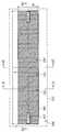
도 1a는 본 발명의 개시의 다양한 양상에 따른 일부 또는 전체의 퓨즈 장치(200)의 평면도이다. 도 1b는 도 1a 내의 라인 1B-1B를 따라 퓨즈 장치의 개략적 단면도이다. 도 1c는 도 1a 내의 라인 1C-1C를 따라 퓨즈 장치(200)의 개략적인 단면도이다. 도 1d는 도 1a 내의 라인 1D-1D를 따라 퓨즈 장치(200)의 개략적인 단면도이다. 퓨즈 장치(200)는 핀형 전계 효과 트랜지스터(FinFET: fin-like field effect transistor) 기반 금속-반도체 합금 퓨즈 장치이다. 용어 FinFET 장치는 임의의 핀-기반, 단일 또는 다중-게이트 트랜지스터를 지칭한다. FinFET 기반, 금속-반도체 합금 퓨즈 장치(200)는 마이크로프로세서, 메모리 셀, 및/또는 다른 집적 회로 장치 내에 포함될 수 있다. 도 1a-1d는 동시에 논의될 것이고, 본 발명의 개시의 진보적인 개념을 더 잘 이해하도록 명료함의 목적을 위해 간략화되었다. 또한, 추가적인 특징이 퓨즈 장치(200)에 추가될 수 있고, 이하 설명된 특징들 중 일부는 퓨즈 장치의 다른 실시에에서 대체되거나 제거될 수 있다.1A is a top view of some or all
금속-반도체 합금 특징 퓨즈 장치(200)는 제1 방향으로 연장하는 크기(dimension)와, 제1 방향과는 다른 제2 방향으로 연장하는 크기를 갖는다. 예를 들면, 퓨즈 장치(200)는 길이 L과 폭 W를 갖는다. 퓨즈 장치(200)는 기판(웨이퍼)(210)을 포함한다. 묘사된 실시예에서, 기판(210)은 실리콘 기판이다. 대안적으로, 또는 추가적으로, 기판(210)은 게르마늄과 같은 원소 반도체와; 실리콘 탄화물, 갈륨 비화물, 갈륨 인화물, 인듐 인화물, 인듐 비화물, 및/또는 인듐 안티몬화물; 또는 이것들의 조합과 같은 화합물 반도체를 포함한다. 대안적으로, 기판(210)은 SOI(silicon-on-insulator) 기판이다. SOI 기판은 산소(SIMOX) 주입, 웨이퍼 본딩, 및/또는 다른 적합한 방법에 의한 분리를 사용해서 제조될 수 있다. 기판(210)은 다양한 도핑된 영역 및 다른 적합한 특징을 포함할 수 있다.The metal-semiconductor alloy
핀(212)을 포함하는 핀 구조는 기판(210)으로부터 연장된다. 퓨즈 장치(200)는 이런 퓨즈 장치(200)의 설계 요구 사항에 따르는 핀(212)을 포함할 수 있다. 묘사된 실시예에서, 핀(212)은 기판(210)의 연장부이고, 실리콘을 포함한다. 핀(212)은 다른 물질 부분을 포함할 수 있다. 핀 구조는 리소그래피 및 에칭 공정을 구현함으로써 형성된다. 예를 들면, 기판(210)으로부터 시작하여, 리소그래피 및 에칭 공정은 기판(210) 내에 트렌치를 형성하고, 이에 따라 기판(210)으로부터 연장되는 핀(212)을 형성한다. 리소그래피 공정은 레지스트 코딩(예, 스핀-온 코팅), 소프트 베이킹, 마스크 정렬, 노출, 사후-노출 베이킹, 레지스트 현상, 세정, 건조(예, 하드 베이킹), 다른 적합한 공정, 또는 이러한 것들의 조합을 포함할 수 있다. 대안적으로, 리소그래피 공정이 구현되거나, 마스크없는(maskless) 리소그래피, 전자-빔 기록, 이온-빔 기록, 및/또는 나노임프린트 기술과 같은 다른 방법들에 의해 구현되거나 대체될 수 있다. 에칭 공정은 건식 에칭 공정, 습식 에칭 공정, 다른 적합한 에칭 공정, 또는 이것들의 결합을 포함한다. 한 예시에서, 핀(212)은 레지스트를 포함하는 마스킹 요소를 형성하기 위해, 기판(210) 위에 레지스트층을 형성하고, 레지스트를 패턴에 노출시키고, 레지스트를 현상(developing)시킴으로써 형성된다. 그런 다음, 예를 들면, 반응 이온 에칭(RIE: reactive ion etch)을 사용함으로써 핀(212)을 기판(210) 내로 에칭하기 위해 마스킹 요소가 사용될 수 있다. 핀(212)은 이중-패터닝 리소그래피(DPL: double-patterning lithography)에 의해 형성될 수 있다. DPL은 패턴을 두 개의 인터리빙된 패턴으로 분리시킴으로써 기판상에 패턴을 구축하는 방법이다. DPL은 강화된 특징(예, 핀) 밀도를 허용한다. 이중 노출(예, 두 개의 마스크 세트를 사용함), 레지스트 냉각, 다른 적합한 공정, 또는 이러한 것들의 결합을 포함하는 다양한 DPL 방법론이 사용될 수 있다.The fin structure, including the
STI(shallow trench isolation) 구조 및/또는 LOCOS(local oxidation of silicon) 구조와 같은 분리 특징부(220)는 핀 구조{묘사된 실시예에서, 핀(212)}를 둘러싸고, 핀들(212)을 서로 분리시킨다. 퓨즈 장치(200)가 마이크로프로세서, 메모리 셀, 또는 다른 집적 회로 장치의 일부분인 상황에서, 분리 특징부(220)는 다른 장치 및/또는 이러한 마이크로프로세서, 메모리 셀, 또는 다른 집적회로 장치의 특징부로부터 퓨즈 장치(200)를 분리시킬 수 있다. 분리 특징부(220)는 실리콘산화물, 실리콘질화물, 실리콘산화질화물, 다른 적합한 물질, 또는 이러한 것들의 조합을 포함한다. 묘사된 실시예에서, 분리 특징부(220)는 실리콘산화물과 같은 산화 물질을 포함한다. 채워진 트렌치는 다중층 구조, 예를 들면, 트렌치를 채우는 실리콘질화물을 갖는 열 산화 라이너층이다. 분리 특징부(212)는 임의의 적합한 공정에 의해 형성된다. 예를 들면, 묘사된 실시예에서, 분리 특징부(220)는 절연 물질을 사용해 핀(212)을 형성하도록 기판(210) 내에 에칭된 트렌치를 완전히 또는 부분적으로 채움으로써 형성될 수 있다.Isolation features 220, such as shallow trench isolation (STI) structures and / or local oxidation of silicon (LOCOS) structures, surround fin structures (in the depicted embodiment, fins 212) and pins 212 to each other. Isolate. In situations where
에피택샬 특징부(230)는 핀 구조의 각 핀(212) 위에 배치된다. 묘사된 실시예에서, 에피택샬 특징부(230)는 연속적 애피택샬 특징부(235)를 형성하도록 함께 병합된다. 에피택샬 특징부(230)는 핀(212)의 노출된 부분상에 반도체 물질을 에피택샬하게(epi) 성장시킴으로써 형성된다. 묘사된 실시예에서, 핀(212)의 에피택샬 특징부(230)가 연속적인 애피택샬 특징부(235)를 형성하도록 함께 병합될 때까지, 반도체 물질이 epi 공정에 의해 에피택샬하게 성장된다. 에피택시 공정은 {증기상 에피택시(VPE: vapor-phase epitaxy) 및/또는 초고진공화학기상증착(UHV-CVD: ultra-high vacuum CVD)과 같은} CVD 증착 기술, 분자빔 에피택시, 다른 적합한 공정, 또는 이것들의 조합을 사용할 수 있다. 에피택샬 공정은 기체 및/또는 액체 전구체를 사용할 수 있다. 묘사된 실시예에서, 에피택샬 특징부(230)(그리고 이에 따라 연속적 에피택샬 특징부(235)}는 실리콘 게르마늄 에피택샬 공정에 의해 형성되는 실리콘 게르마늄(SiGe)을 포함한다. 실리콘 게르마늄은 기판(210)의 열 전달을 감소시킬 수 있다. 대안적으로, 에피택샬 특징부(230){연속적인 에피택샬 특징부(235)}는 다른 에피택샬 물질을 포함한다. 이러한 에피택샬 물질은 낮은 열 전도성과 같은 바람직한 열 특성을 갖는 에피택샬 물질로부터 선택될 수 있다. 예를 들면, 선택된 에피택샬 물질은 기판(210)으로의 열 전도를 감소시키는 열 저항성을 나타낼 수 있다. 에피택샬 특징부(230){연속적 에피택샬 특징부(235)}는 불순물을 에피택시 공정의 소스물질에 첨가함으로써 증착(성장) 동안에, 또는 이온 주입 공정에 의한 증착 성장 공정에 후속하여 도핑될 수 있다. 도핑된 에피택샬층은 경사(gradient) 도핑 프로파일을 가질 수 있다. 화학 기계적 폴리싱(CMP: chemical mechanical polishing)은 애피택샬 특징부(230){연속적 에피택샬 특징부(235)}를 평탄화하기 위해 수행될 수 있다.The
금속-반도체 합금 특징부(240)는 에피택샬 특징부(230) 위에 배치되고, 그리고 묘사된 실시예에서, 연속적 에피택샬 특징부(235) 위에 배치된다. 묘사된 실시예에서, 금속-반도체 합금 특징부(240)는 니켈 규화물, 코발드 규화물, 텅스텐 규화물, 탄탈륨 규화물, 티타늄 규화물, 백금 규화물, 에르븀 규화물, 팔라듐 규화물, 다른 적합한 규화물, 또는 이것들의 조합과 같은 규화물을 포함한다. 금속-반도체 합금 특징부(240)는 자가-정렬되는 규화물(살리사이드) 공정과 같은 규화물화 공정에 의해 형성될 수 있다.Metal-semiconductor alloy features 240 are disposed over
접촉부(250)는 금속-반도체 합금 특징부(240) 위에 배치되고, 이러한 특징부(240)와 전기적으로 연결된다. 금속-반도체 합금 특징부(240)는 연속적으로 연장되고, 접촉부들(250) 사이에서 끊어지지 않으며, 금속-반도체 합금(240)은 퓨즈 장치(200)의 퓨즈 요소로서 역할을 한다. 접촉부(250)는 알루미늄, 구리, 티타늄, 탄탈륨, 텅스텐과 같은 전도성 물질, 다른 전도성 물질, 또는 이것들의 조합을 포함한다. 묘사된 실시예에서, 접촉부(250) 중 하나는 퓨즈 장치(200)의 애노드이고, 접촉부(250) 중 하나는 퓨즈 장치(200)의 캐소드이다.Contact 250 is disposed over metal-semiconductor alloy features 240 and is electrically connected to these
동작 중에, 접촉부(250)는 바이어스되어(전압이 여기에 인가됨), 전류는 애노드로서 작용하는 접촉부(250)로 흘러 금속-반도체 합금 특징부(240)를 통해 캐소드로서 작용하는 접촉부(250)로 흐른다. 퓨즈 장치(200)의 프로그래밍 전류가 접촉부(250)를 바이어싱함으로서 도달될 때, 불연속성이 금속-반도체 합금 특징부(240) 내에 발생하여, 전류가 금속-반도체 합금 특징부(240)를 경유해 애노드로부터 캐소드로 흐르는 것을 방지하여, 이에 따라 퓨즈 장치(200)를 끊어지게 한다(blowing). 예를 들면, 불연속성은 금속-반도체 합금 특징부(240)의 일부분이 흐르는 전류에 의해 발생된 열에 의해 용융될 때, 발생할 수 있다. 동작 동안에, 애노드로부터 금속-반도체 합금 특징부(240)를 경유해 캐소드로 흐르는 전류에 의해 발생된 열은 에피택샬 특징부(230){묘사된 실시예에서, 연속적 에피택샬 특징부(235)}와 분리 특징부(220)에 의해 기판(210) 안으로 흐르는 것이 제약된다. 이러한 열 제약은 퓨즈 장치(200)가 설계된 프로그래밍 전류에서 끊기는 것을 보장할 수 있다.In operation, contact 250 is biased (voltage is applied thereto) so that current flows into
퓨즈 장치(200)의 퓨즈 요소와 금속-반도체 합금 특징부(240)의 특징은 종래의 퓨즈 장치에서 구현된 폴리실리콘 퓨즈 요소의 특징과 유사할 수 있다. 예를 들면, 폴리실리콘 퓨즈 요소를 구비한 퓨즈 장치와 유사하게, 금속-반도체 합금 특징부(240)(금속-반도체 합금 퓨즈 요소)를 구비한 퓨즈 장치(200)는 구리 퓨즈 요소를 구비한 종래의 퓨즈 장치를 위해 요구되는 것보다 낮은 프로그래밍 전류에서 기능한다. 구체적으로, 퓨즈 장치(200)의 프로그래밍 전류는 구리 퓨즈 요소를 구비한 퓨즈 장치의 프로그래밍 전류보다 한 차수(order)만큼 더 낮을 수 있다{예를 들면, 금속-반도체 합금 퓨즈 요소를 구비한 퓨즈 장치의 프로그래밍 전류는 약 2.00 x 10⁻³ A(암페어)일 수 있는 반면에, 구리 퓨즈 요소를 구비한 퓨즈 장치의 프로그래밍 전류는 약 1.75 x 10⁻²A 일 수 있다}는 것이 관찰되었다. 묘사된 실시예에서, 상술된 것처럼, 에피택샬 특징부(230){연속적 에피택샬 특징부(235)}는 동작 중에 발생되는 열이 기판(210)으로 흘러가는 것을 방지하거나 감소시킴으로써 금속-반도체 합금 특징부(240)(금속-반도체 합금 퓨즈 요소)를 구비한 퓨즈 장치(200)의 더 낮은 프로그래밍 전류를 유지하는데 기여한다. 또한, 이하에서 더 설명되는 바와 같이, 바람직한 프로그래밍 전류를 제공하면서, 금속-반도체 합금 특징부(240)(금속-반도체 합금 퓨즈 요소)를 구비한 퓨즈 장치(200)는 폴리실리콘 퓨즈 요소를 구비한 퓨즈 장치와 비교해서, 고-k/금속 게이트 처리에서 쉽게 구현된다. 따라서, 퓨즈 장치(200)는 폴리실리콘 퓨즈 요소를 구비한 퓨즈 장치에 의해 달성되는 특징과 같은 바람직한 동작 특징을 달성하는 한편, 구리 퓨즈 요소를 구비한 퓨즈 장치에 의해 달성되는 호환성과 같이, 종래 처리시에 바람직한 호환성을 달성한다. 심지어 더 나아가, 구리 퓨즈 요소를 구비한 퓨즈 장치와 비교할 때, 금속-반도체 합금 특징부(240)(금속-반도체 합금 퓨즈 요소)를 구비한 퓨즈 장치(200)는 후속 공정 개발 및 최적화 동안 그 특징을 유지할 수 있어서, 나중의 공정 개발 단계들에서 가능한 설계 변경을 최소화할 수 있다. 상이한 실시예들은 상이한 이점을 가질 수 있고, 어떠한 특별한 이점은 임의의 실시예를 위해 필연적으로 요구되지 않는다.Features of the fuse element and metal-
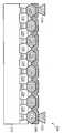
도 2a는 본 발명의 개시의 다양한 양상에 따른 일부 또는 전체의 퓨즈 장치(300)의 평면도이다. 도 2b는 도 2a 내의 라인 2B-2B를 따라 퓨즈 장치(300)의 개략적인 단면도이다. 도 2c는 도 2a 내의 라인 2C-2C를 따라 퓨즈 장치의 개략적인 단면도이다. 도 2d는 도 2a 내의 라인 2D-2D를 따라 퓨즈 장치의 개략적인 단면도이다. 도 2a-2d는 동시에 논의될 것이고, 본 발명의 개시의 진보적인 개념을 더 잘 이해하도록 명료함의 목적을 위해 간략화되었다. 도 2a 내지 2d의 실시예는 도 1a 내지 1d의 실시예와 많은 측면에서 유사하다. 따라서, 도 1a 내지 1d와 도 2a 내지 2d의 유사한 특징들은 명료함과 간략화를 위해 동일 참조 번호들에 의해 식별된다. 퓨즈 장치(300)에서, 에피택샬 특징부(230)는 연속적 애피택샬 특징부(235)를 형성하도록 함께 병합되지 않는다. 하지만, 에피택샬 특징부(230)는 서로 근접하여, 에피택샬 특징부(230) (에피택샬 아일랜드라고 또한 지칭됨)상에 형성된 금속-반도체 합금 특징부는 금속-반도체 합금 특징부(240)를 형성하기 위해 함께 병합되어, 접촉부들(250) 사이에서 연속적으로 연장되고 끊어지지 않게 된다. 예시에서, 인접 에피택샬 특징부들(230)간의 거리는 약 10 nm 이하이다. 추가적인 특징부는 퓨즈 장치(300)에 추가될 수 있고, 이하에서 설명되는 특징부들 중 일부는 퓨즈 장치(300)의 다른 실시예를 위해 대체되거나 제거될 수 있다.2A is a top view of some or all
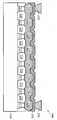
도 3a는 본 발명의 개시의 다양한 양상에 따른 일부 또는 전체의 퓨즈 장치(400)의 평면도이다. 도 3b는 도 3a 내의 라인 3B-3B를 따라 퓨즈 장치(400)의 개략적인 단면도이다. 도 3c는 도 3a 내의 라인 3C-3C를 따라 퓨즈 장치(400)의 개략적인 단면도이다. 도 3d는 도 3a 내의 라인 3D-3D를 따라 퓨즈 장치(400)의 개략적인 단면도이다. 도 3a 내지 3d는 동시에 논의될 것이고, 본 발명의 개시의 진보적인 개념을 더 잘 이해하도록 명료함의 목적을 위해 간략화되었다. 도 3a 내지 3d의 실시예는 도 1a 내지 1d의 실시예와 많은 측면에서 유사하다. 따라서, 도 1a 내지 1d와 도 3a 내지 3d의 유사한 특징들은 명료함과 간략화를 위해 동일 참조 번호들에 의해 식별된다. 추가적인 특징부는 퓨즈 장치(400)에 추가될 수 있고, 이하에서 설명되는 특징부들 중 일부는 퓨즈 장치(400)의 다른 실시예를 위해 대체되거나 제거될 수 있다.3A is a top view of some or all
퓨즈 장치(400)에서, 게이트 구조(450)는 퓨즈 장치(400)의 폭(W)을 제어하거나 한정한다. 게이트 구조(450)는 핀(212)을 횡단하고, 묘사된 실시예에서, 핀(212)의 적어도 두 부분을 횡단하여, 금속-반도체 합금 특징부(240)가 처리 동안에 게이트 구조(450) 사이에 형성된다. 따라서, 퓨즈 장치(400)의 폭은 리소그래피 처리에 의해 허용되는 분해능(resolution) 한도 미만과 같이, 종래 처리에 의해 달성가능한 폭 미만일 수 있다. 퓨즈 장치(400)가 마이크로프로세서, 메모리 셀, 또는 다른 집적회로 장치에 포함되는 상황에서, 게이트 구조(450)는 마이크로프로세서, 메모리 셀, 또는 다른 집적회로 장치의 다른 장치의 게이트 구조와 동시에 형성될 수 있는 더미 게이트 구조이다. 게이트 구조(450)는 증착 공정, 리소그래피 패터닝 공정, 에칭 공정을 포함하는 적합한 공정, 다른 적합한 공정, 또는 이것들의 조합에 의해 형성된다. 증착 공정은 화학 증기 증착(CVD), 물리 증기 증착(PVD), 원자층 증착(ALD), 고밀도 플라즈마 CVD(HDPCVD), 금속 유기 CVD(MOCVD), 원격 플라즈마 CVD(RPCVD), 플라즈마 강화 CVD(PECVD), 저압 CVD(LPCVD), 원자층 CVD(ALCVD), 대기압 CVD(APCVD), 도금, 다른 적합한 방법, 또는 이것들의 결합을 포함한다. 리소그래피 패터닝 공정은 레지스트 코딩(예, 스핀-온 코팅), 소프트 베이킹, 마스크 정렬, 노출, 사후-노출 베이킹, 포토레지스트 현상, 세정, 건조(예, 하드 베이킹), 다른 적합한 공정, 또는 이러한 것들의 조합을 포함할 수 있다. 대안적으로, 리소그래피 노출 공정은 마스크리스(maskless) 리소그래피, 전자-빔 기록, 또는 이온-빔 기록과 같은 다른 방법에 의해 구현되거나 대체된다. 다른 대안에서, 리소그래피 패터닝 공정은 나노임프린트 기술을 구현할 수 있다. 에칭 공정은 건식 에칭, 습식 에칭, 다른 에칭 방법, 또는 이것들의 조합을 포함한다.In the
게이트 구조(450)는 게이트 스택을 포함하며, 이러한 게이트 스택은 게이트 유전체(452)와 게이트 전극(454)을 포함한다. 게이트 구조(450)의 게이트 스택은 예를 들면, 캡핑(capping)층, 인터페이스층, 확산층, 장벽층, 하드 마스크층, 또는 이것들의 조합과 같은 다수의 다른 층들을 포함할 수 있다. 게이트 유전체(452)는 실리콘산화물, 고-k 유전물질과 같은 유전물질, 다른 적합한 유전물질, 또는 이것들의 조합을 포함한다. 고-k 유전 물질의 예시는 HfO2, HfSiO, HfSiON, HfTaO, HfTiO, HfZrO, 지르코늄산화물, 알루미늄산화물, 하프늄산화물-알루미나(HfO2-Al2O3) 합금, 다른 적절한 고-k 유전 물질, 또는 이것들의 조합을 포함한다. 게이트 전극(454)은 폴리실리콘, 및/또는 Al, Cu, Ti, Ta, W, Mo, TaN, NiSi, CoSi, TiN, WN, TiAl, TiAlN, TaCN, TaC, TaSiN을 포함하는 금속, 다른 전도성 물질, 또는 이것들의 조합을 포함한다. 묘사된 실시예에서, 게이트 전극(254)은 금속을 포함하고, 게이트 마지막(last) 공정에서 형성된다.
게이트 구조는 스페이서(456)를 더 포함한다. 스페이서(456)는 게이트 유전체(452)와 게이트 전극(454)의 측벽을 따라서 배치되는 것과 같이, 게이트 구조(450)의 게이트 스택의 측벽상에 배치된다. 스페이서(456)는 실리콘산화물, 실리콘질화물, 실리콘산화질화물, 다른 적합한 물질, 또는 이러한 것들의 조합을 포함한다. 스페이서(456)는 실리콘질화물층과 실리콘산화물층을 포함하는 다중층 구조와 같은 다중층 구조를 포함할 수 있다. 스페이서는 적절한 두께로 적절한 공정에 의해 형성된다. 예를 들면, 묘사된 실시예에서, 도 3c 내지 3d에 예증된 것처럼, 스페이서(456)는 실리콘질화물층을 증착하고, 그런 다음 스페이서(456)를 형성하기 위해 이러한 실리콘질화물층을 건식 에칭함으로써 형성될 수 있다.The gate structure further includes a
도 4는 본 발명의 개시의 다양한 양상에 따른 일부 또는 전체의 퓨즈 장치(500)의 평면도이다. 도 4의 실시예는 도 1a 내지 1d, 도 2a 내지 2d와, 도 3a 내지 3d의 실시예와 많은 측면에서 유사하다. 따라서, 도 1a 내지 1d, 도 2a 내지 2d, 도 3a 내지 3와, 및 도 4의 유사한 특징들은 명료함과 간략화를 위해 동일 참조 번호들에 의해 식별된다. 묘사된 실시예에서, 퓨즈 장치(500)는 비대칭 형태를 갖는다. 예를 들면, 퓨즈 장치(500)는 제1 부분(500A)과 제2 부분(500B)를 가지고, 접촉부(250) 중 하나는 제1 부분(500A) 위에 배치되고, 이러한 제1 부분에 연결되고, 접촉부(250) 중 하나는 제2 부분(500B) 위에 배치되고, 이러한 제2 부분(500B)에 연결된다. 제1 부분(500A)의 폭(W1)은 제2 부분(500B)의 폭보다 작다. 처리 동안에, 게이트 구조(450)는 묘사된 실시예에서처럼 제1 부분(500A)의 폭(W1)을 한정하기 위해 형성될 수 있다. 동작시에, 퓨즈 장치(500)의 비대칭 형태는 온도 경사(gradient)를 생성하여, 퓨즈 장치(500)가 끊어지기(break) 더 쉽게 된다. 예를 들면, 전류가 접촉부(250)들 사이에서 금속-반도체 합금 특징부(240)를 경유해 이동할 때, 제1 부분(500A)의 폭(W1)이 제2 부분(500B)의 폭(W2)보다 작기 때문에, 제1 부분(500A)에서의 전류 밀도가 제2 부분(500B)에서의 전류 밀도보다 크게 되어, 제1 부분(500A)에서의 열 에너지(및 온도)가 제2 부분(500B)에서의 열 에너지(및 온도)보다 크게 된다. 이러한 온도 경사(gradient)는 퓨즈 장치(500)를 끊기 위한 향상된 프로그래밍 전류 능력과 같은 향상된 프로그래밍가능성(programmability)을 제공할 수 있다. 퓨즈 장치(500)의 비대칭 형태는 단지 예시일뿐이고, 원하는 프로그래밍가능성을 달성하는 다른 비대칭 형태의 퓨즈 장치가 고려된다는 것이 주목된다. 추가적인 특징부는 퓨즈 장치(500)에 추가될 수 있고, 이하에서 설명되는 특징부들 중 일부는 퓨즈 장치(500)의 다른 실시예를 위해 대체되거나 제거될 수 있다.4 is a top view of some or all
도 5는 본 발명의 개시의 다양한 양상에 따른 집적회로 장치를 제조하는 방법(600)의 흐름도이다. 묘사된 실시예에서, 방법(600)은 퓨즈 장치, 특히, 도 1a 내지 1d, 도 2a 내지 2d, 도 3a 내지 3d와 도 4를 각각 참조하여 위에서 설명된 퓨즈 장치(200, 300, 400과 500)와 같은 퓨즈 장치, 즉, 구체적으로는, FinFET 기반 금속-반도체 합금 퓨즈 장치를 포함하는 집적회로 장치를 제조한다. 방법(600)은 복수의 핀이 기판 위에 형성되는 블록(610)에서 시작한다. 기판은 기판(210)과 유사할 수 있고, 핀은 위에서 설명된 핀(212)와 유사할 수 있다. 블록(620)에서, 에피택샬층은 복수의 핀 각각 위에 형성된다. 에피택샬층은 위에서 설명된 에피택샬 특징부(230){또는 연속적 에피택샬 특징부(235)}와 유사할 수 있다. 블록(630)에서, 금속-반도체 합금 특징부는 에피택샬층 위에서 형성된다. 금속-반도체 합금 특징부는 위에서 설명된 금속-반도체 합금 특징부(240)와 유사할 수 있다. 블록(640)에서, 제1 접촉부와 제2 접촉부가 형성되어 금속-반도체 합금 특징부와 연결되고, 금속-반도체 합금 특징부는 제1 접촉부와 제2 접촉부 사이에서 연속적으로 연장된다. 제1 및 제2 접촉부는 위에서 설명된 접촉부(250)와 유사할 수 있다. 방법(600)은 집적회로 장치의 제조를 완료하기 계속 진행할 수 있다. 추가적인 단계들이 방법(600) 이전, 동안, 및 이후에 제공될 수 있고, 설명된 단계들 중 일부는 방법(600)의 다른 실시예를 위해 대체되거나 제거될 수 있다. 예를 들면, 에피택샬층이 복수의 핀 각각 위에 형성되기 전에, 복수의 핀을 횡단하는 게이트 구조가 형성될 수 있다. 게이트 구조는 위에서 설명된 게이트 구조(450)와 유사할 수 있다. 그러므로, 금속-반도체 합금 특징부는 게이트 구조들 사이에서 형성되는 것으로 제한될 수 있다. 한 예시에서, 게이트 구조는 고-k 게이트 유전층과 같은 게이트 유전체와, 폴리실리콘 게이트 전극과 같은 더미 게이트 전극을 포함한다. 이러한 예시에 따라, 금속-반도체 합금 특징부가 형성된 후에, 더미 게이트 전극이 금속 게이트로 대체될 수 있다.5 is a flowchart of a
방법(600)은 여기서 설명된 퓨즈 장치를 형성할 수 있는 한편, 이와 동시에 집적회로 장치의 다른 장치들을 형성할 수 있다. 예를 들면, 방법(600)은 FinFET 기반 금속-반도체 합금 퓨즈 장치와, 집적회로 장치의 FinFET 장치를 동시에 형성할 수 있다. 따라서, 여기서 설명된 퓨즈 장치는 종래의 상보형금속산화반도체(CMOS: complementary metal-oxide-semiconductor) 처리, 특히, 고-k/금속 게이트 CMOS 처리와 호환된다. 따라서, 제조 비용과 제조 시간은 집적회로 장치 제조시에 설명된 퓨즈 장치를 구현하는 것에 의해 부정적인 영향을 받지 않는다. 상이한 실시예들은 상이한 이점을 가질 수 있고, 어떠한 특별한 이점도 임의의 실시예를 위해 필연적으로 요구되지 않는다.The
본 발명 개시는 많은 상이한 실시예들을 제공한다. 한 예시에서, 장치는 반도체 기판과, 반도체 기판 위에 배치된 핀 구조를 포함하고, 핀 구조는 기판 위에 배치된 적어도 두 개의 핀과, 적어도 두 개의 핀 각각 위에 배치된 에피택샬 반도체 특징부와, 적어도 두 개의 핀 각각의 에피택샬 반도체 특징부 위에 배치된 금속-반도체 합금 특징부와, 금속-반도체 합금 특징부와 연결된 제1 접촉부와 제2 접촉부를 포함하고, 금속-반도체 합금 특징부는 제1 접촉부와 제2 접촉부 사이에서 연속적으로 연장된다. 적어도 두 개의 핀 각각 위에 배치된 에피택샬 반도체 특징부는 적어도 두 개의 핀 각각 위에 배치된 연속적 에피택샬 특징부를 형성하도록 함께 병합될 수 있다. 에피택샬 반도체 특징부는 실리콘 게르마늄을 포함할 수 있다. 금속-반도체 합금 특징부는 규화물을 포함할 수 있다. 반도체 기판은 SOI(silicon-on-insulator) 기판일 수 있다. 금속-반도체 합금 특징부의 폭은 적어도 두 개의 게이트 구조에 의해 한정될 수 있고, 적어도 두 개의 게이트 구조 각각은 적어도 두 개의 핀을 횡단한다. 한 예시에서, 적어도 두 개의 게이트 구조는 적어도 두 개의 핀 위에 배치된 게이트 유전층과, 게이트 유전층 위에 배치된 게이트 전극을 구비한 게이트 스택을 포함한다. 게이트 유전층은 고-k 게이트 유전층일 수 있고, 게이트 전극은 금속 게이트 전극일 수 있다.The present disclosure provides many different embodiments. In one example, an apparatus includes a semiconductor substrate, a fin structure disposed over the semiconductor substrate, the fin structure comprising at least two fins disposed over the substrate, epitaxial semiconductor features disposed over each of the at least two fins, at least A metal-semiconductor alloy feature disposed over the epitaxial semiconductor feature of each of the two fins, and a first contact and a second contact connected with the metal-semiconductor alloy feature, wherein the metal-semiconductor alloy feature includes: It extends continuously between the second contacts. The epitaxial semiconductor features disposed over each of the at least two fins may be merged together to form a continuous epitaxial feature disposed over each of the at least two fins. The epitaxial semiconductor feature may comprise silicon germanium. Metal-semiconductor alloy features may include silicides. The semiconductor substrate may be a silicon-on-insulator (SOI) substrate. The width of the metal-semiconductor alloy features can be defined by at least two gate structures, each of the at least two gate structures traversing at least two fins. In one example, at least two gate structures include a gate stack having a gate dielectric layer disposed over at least two fins and a gate electrode disposed over the gate dielectric layer. The gate dielectric layer may be a high-k gate dielectric layer and the gate electrode may be a metal gate electrode.
다른 예시에서, 퓨즈 장치는 금속-반도체 합금층과 연결된 제1 접촉부와 제2 접촉부를 포함하고, 금속-반도체 합금층은 제1 접촉부와 제2 접촉부 사이에서 연속적으로 연장된다. 금속-반도체 합금층은 기판의 핀 구조 위에 배치된 에피택샬층 위에 배치된다. 한 예시에서, 기판과 핀 구조는 실리콘을 포함하고, 에피택샬층은 실리콘 게르마늄을 포함하고, 금속-반도체 합금층은 니켈 규화물, 코발트 규화물, 텅스텐 규화물, 탄탈륨 규화물, 티타늄 규화물, 백금 규화물, 에르븀 규화물, 팔라듐 규화물, 또는 이것들의 조합과 같은 규화물을 포함한다. 에피택샬층은 핀 구조의 핀들 사이에서 연속적으로 연장된다. 에피택샬층은 핀 구조의 핀들 사이에 갭(gap)을 포함할 수 있고, 금속-반도체 합금층은 적어도 부분적으로 갭을 채운다. 금속-반도체 합금 특징부는 핀 구조의 핀들을 횡단하는 게이트 구조들 사이에 배치될 수 있다. 한 예시에서, 금속-반도체 합금 특징부는 제1 폭을 갖는 제1 부분과, 제2 폭을 갖는 제2 부분을 가지며, 제2 폭은 제1 폭보다 크고, 제1 접촉부는 제1 부분과 연결되고, 제2 접촉부는 제2 부분과 연결된다. 금속-반도체 합금 특징부의 제1 부분은 핀 구조의 핀들을 횡단하는 게이트 구조들 사이에 배치될 수 있어서, 제1 부분의 제1 폭은 게이트 구조에 의해 한정된다.In another example, the fuse device includes a first contact portion and a second contact portion connected with the metal-semiconductor alloy layer, and the metal-semiconductor alloy layer extends continuously between the first contact portion and the second contact portion. The metal-semiconductor alloy layer is disposed over the epitaxial layer disposed over the fin structure of the substrate. In one example, the substrate and fin structure comprises silicon, the epitaxial layer comprises silicon germanium, and the metal-semiconductor alloy layer includes nickel silicide, cobalt silicide, tungsten silicide, tantalum silicide, titanium silicide, platinum silicide, erbium silicide Silicides such as palladium silicides, or combinations thereof. The epitaxial layer extends continuously between the fins of the fin structure. The epitaxial layer may include a gap between the fins of the fin structure, and the metal-semiconductor alloy layer at least partially fills the gap. The metal-semiconductor alloy feature may be disposed between gate structures traversing the fins of the fin structure. In one example, the metal-semiconductor alloy feature has a first portion having a first width and a second portion having a second width, the second width is greater than the first width, and the first contact connects with the first portion. And the second contact portion is connected with the second portion. The first portion of the metal-semiconductor alloy feature may be disposed between gate structures traversing the fins of the fin structure, such that the first width of the first portion is defined by the gate structure.
다른 예시에서, 방법은 기판 위에 복수의 핀을 형성하는 단계, 복수의 핀 각각 위에 에피택샬층을 형성하는 단계, 에피택샬층 위에 금속-반도체 합금 특징부를 형성하는 단계, 금속-반도체 합금 특징부와 연결된 제1 접촉부와 제2 접촉부를 형성하는 단계를 포함하고, 금속-반도체 합금 특징부는 제1 접촉부와 제2 접촉부 사이에서 연속적으로 연장된다. 복수의 핀 각각 위에 에피택샬층을 형성하는 단계는 복수의 핀 각각 상에 성장한 반도체 물질이 연속적 에피택샬층을 형성하도록 함께 병합될 때까지 복수의 핀 각각 상에 반도체 물질을 에피택샬하게 성장시키는 단계를 포함할 수 있다. 방법은 에피택샬층을 형성하기 전에 복수의 핀을 횡단하는 게이트 구조를 형성하는 단계를 더 포함할 수 있다. 방법은 금속-반도체 합금 특징부를 형성한 후에 게이트 구조의 더미 게이트를 금속 게이트로 대체시키는 단계를 더 포함할 수 있다.In another example, a method includes forming a plurality of fins over a substrate, forming an epitaxial layer over each of the plurality of fins, forming a metal-semiconductor alloy feature over the epitaxial layer, a metal-semiconductor alloy feature and Forming a connected first contact and a second contact, wherein the metal-semiconductor alloy feature extends continuously between the first contact and the second contact. Forming an epitaxial layer over each of the plurality of fins comprises epitaxially growing semiconductor material on each of the plurality of fins until the semiconductor material grown on each of the plurality of fins is merged together to form a continuous epitaxial layer. It may include. The method may further include forming a gate structure crossing the plurality of fins before forming the epitaxial layer. The method may further include replacing the dummy gate of the gate structure with a metal gate after forming the metal-semiconductor alloy feature.
전술된 내용은 여러 실시예들의 특징의 개요를 서술하여, 당업자는 본 발명의 개시의 양상을 더 잘 이해할 수 있다. 당업자는 자신들이 여기서 소개된 실시예들의 동일한 목적을 수행하기 위해 및/또는 동일한 이익을 달성하도록 다른 공정 및 구조를 설계하거나 수정하기 위한 기초로서 본 발명의 개시를 쉽게 사용할 수 있다는 것을 인식해야 한다. 당업자는 이러한 등가의 구성이 본 발명의 개시의 정신 및 범위로부터 이탈하지 않는다는 것과, 본 발명의 개시의 정신 및 범위로부터 이탈하지 않고 다양한 변경, 교체 및 대체를 할 수 있다는 것을 또한 인식해야 한다.The foregoing describes an overview of the features of the various embodiments, and one skilled in the art can better understand the aspects of the disclosure of the present invention. Those skilled in the art should appreciate that they can readily use the present disclosure as a basis for designing or modifying other processes and structures to accomplish the same purpose of the embodiments disclosed herein and / or to achieve the same benefits. Those skilled in the art will appreciate that such equivalent constructions do not depart from the spirit and scope of the disclosure of the invention and that various changes, substitutions and substitutions can be made without departing from the spirit and scope of the disclosure of the invention.
Claims (10)
Translated fromKorean상기 반도체 기판 위에 배치된 핀 구조 - 상기 핀 구조는 상기 기판 위에 배치된 적어도 두 개의 핀을 포함함 -;
상기 적어도 두 개의 핀의 인접 핀들 사이에 형성된 유전체 분리 특징부;
상기 적어도 두 개의 핀 각각 위에 배치된 에피택샬(epitaxial) 반도체 특징부;
상기 적어도 두 개의 핀 각각의 에피택샬 반도체 특징부 위에 배치된 금속-반도체 합금 특징부; 및
상기 금속-반도체 합금 특징부와 연결된 제1 접촉부와 제2 접촉부를
포함하고,
상기 금속-반도체 합금 특징부는 상기 제1 접촉부와 상기 제2 접촉부 사이에서 연속적으로 연장하는 것인 장치.A semiconductor substrate;
A fin structure disposed over the semiconductor substrate, the fin structure comprising at least two fins disposed over the substrate;
Dielectric isolation features formed between adjacent fins of the at least two fins;
An epitaxial semiconductor feature disposed over each of the at least two fins;
A metal-semiconductor alloy feature disposed over the epitaxial semiconductor feature of each of the at least two fins; And
A first contact portion and a second contact portion connected to the metal-semiconductor alloy feature
Including,
And the metal-semiconductor alloy feature extends continuously between the first contact and the second contact.
금속-반도체 합금층과 연결되는 제1 접촉부와 제2 접촉부를 포함하는 퓨즈 장치를 포함하고,
상기 금속-반도체 합금층은 상기 제1 접촉부와 상기 제2 접촉부 사이에서 연속적으로 연장되고, 상기 금속-반도체 합금층은 복수의 핀을 포함하는 기판의 핀 구조 위에 배치된 에피택샬층 위에 배치되며,
상기 금속-반도체 합금층은 상기 복수의 핀의 인접 핀들 사이에 배치된 유전체 분리 특징부 위에 배치되는 것인, 집적회로 장치.In an integrated circuit device,
A fuse device comprising a first contact portion and a second contact portion connected with the metal-semiconductor alloy layer,
The metal-semiconductor alloy layer extends continuously between the first contact portion and the second contact portion, the metal-semiconductor alloy layer is disposed over an epitaxial layer disposed over a fin structure of a substrate including a plurality of fins,
And the metal-semiconductor alloy layer is disposed over a dielectric isolation feature disposed between adjacent fins of the plurality of fins.
상기 기판과 상기 핀 구조는 실리콘을 포함하고,
상기 에피택샬층은 실리콘 게르마늄을 포함하고,
상기 금속-반도체 합금층은 규화물을 포함하는 것은, 집적회로 장치.5. The method of claim 4,
The substrate and the fin structure comprises silicon,
The epitaxial layer comprises silicon germanium,
And the metal-semiconductor alloy layer comprises silicide.
상기 금속-반도체 합금 특징부는 제1 폭을 갖는 제1 부분과 제2 폭을 갖는 제2 부분을 구비하고, 상기 제2 폭은 상기 제1 폭보다 크고,
상기 제1 접촉부는 상기 제1 부분에 연결되고, 상기 제2 접촉부는 상기 제2 부분에 연결되는 것인, 집적회로 장치.5. The method of claim 4,
The metal-semiconductor alloy feature has a first portion having a first width and a second portion having a second width, wherein the second width is greater than the first width,
And the first contact portion is connected to the first portion and the second contact portion is connected to the second portion.
상기 복수의 핀의 인접 핀들 사이에 유전체 분리 특징부를 형성하는 단계;
상기 복수의 핀 각각 위에 에피택샬층을 형성하는 단계;
상기 에피택샬층 및 상기 유전체 분리 특징부 위에 금속-반도체 합금 특징부를 형성하는 단계와;
상기 금속-반도체 합금 특징부와 연결된 제1 접촉부와 제2 접촉부를 형성하는 단계를 포함하고,
상기 금속-반도체 합금 특징부는 상기 제1 접촉부와 상기 제2 접촉부 사이에서 연속적으로 연장되는 것인 방법.Forming a plurality of fins on the substrate;
Forming a dielectric isolation feature between adjacent fins of the plurality of fins;
Forming an epitaxial layer on each of the plurality of fins;
Forming a metal-semiconductor alloy feature over the epitaxial layer and the dielectric isolation feature;
Forming a first contact and a second contact connected with the metal-semiconductor alloy feature,
And the metal-semiconductor alloy feature extends continuously between the first contact and the second contact.
Applications Claiming Priority (2)
| Application Number | Priority Date | Filing Date | Title |
|---|---|---|---|
| US13/283,127US8969999B2 (en) | 2011-10-27 | 2011-10-27 | Fin-like field effect transistor (FinFET) based, metal-semiconductor alloy fuse device and method of manufacturing same |
| US13/283,127 | 2011-10-27 |
Publications (2)
| Publication Number | Publication Date |
|---|---|
| KR20130046338A KR20130046338A (en) | 2013-05-07 |
| KR101381492B1true KR101381492B1 (en) | 2014-04-04 |
Family
ID=48171510
Family Applications (1)
| Application Number | Title | Priority Date | Filing Date |
|---|---|---|---|
| KR1020120055512AActiveKR101381492B1 (en) | 2011-10-27 | 2012-05-24 | Fin-like field effect transistor (finfet) based, metal-semiconductor alloy fuse device and method of manufacturing same |
Country Status (3)
| Country | Link |
|---|---|
| US (2) | US8969999B2 (en) |
| KR (1) | KR101381492B1 (en) |
| TW (1) | TWI496266B (en) |
Families Citing this family (22)
| Publication number | Priority date | Publication date | Assignee | Title |
|---|---|---|---|---|
| US8969999B2 (en) | 2011-10-27 | 2015-03-03 | Taiwan Semiconductor Manufacturing Company, Ltd. | Fin-like field effect transistor (FinFET) based, metal-semiconductor alloy fuse device and method of manufacturing same |
| US9093453B2 (en)* | 2013-10-07 | 2015-07-28 | International Business Machines Corporation | High performance e-fuse fabricated with sub-lithographic dimension |
| US9165936B2 (en)* | 2014-01-14 | 2015-10-20 | Broadcom Corporation | Dummy end-gate based anti-fuse device for finFET technologies |
| KR102150869B1 (en) | 2014-04-03 | 2020-09-02 | 삼성전자 주식회사 | fuse structure and semiconductor device including the same |
| KR102191221B1 (en)* | 2014-09-23 | 2020-12-16 | 삼성전자주식회사 | Resistor and semiconductor device including the same |
| US9391201B2 (en) | 2014-11-25 | 2016-07-12 | Taiwan Semiconductor Manufacturing Company, Ltd. | Source/drain structure and manufacturing the same |
| KR102150942B1 (en) | 2014-12-01 | 2020-09-03 | 삼성전자주식회사 | Semiconductor device including fin FET |
| US9263385B1 (en)* | 2015-01-05 | 2016-02-16 | Globalfoundries Inc. | Semiconductor fuses and fabrication methods thereof |
| US9293221B1 (en) | 2015-02-26 | 2016-03-22 | International Business Machines Corporation | Three terminal fuse with FinFET |
| KR102317646B1 (en) | 2015-04-14 | 2021-10-27 | 삼성전자주식회사 | Semiconductor device and method for manufacturing the same |
| KR102476356B1 (en) | 2015-10-07 | 2022-12-09 | 삼성전자주식회사 | Integrated circuit device and method of manufacturing the same |
| KR102323943B1 (en) | 2015-10-21 | 2021-11-08 | 삼성전자주식회사 | Method of manufacturing semiconductor device |
| US9613899B1 (en)* | 2015-11-02 | 2017-04-04 | International Business Machines Corporation | Epitaxial semiconductor fuse for FinFET structure |
| JP6636823B2 (en)* | 2016-02-25 | 2020-01-29 | エイブリック株式会社 | Semiconductor device and fuse cutting method |
| US9754875B1 (en) | 2016-07-20 | 2017-09-05 | International Business Machines Corporation | Designable channel FinFET fuse |
| US9929091B2 (en)* | 2016-08-25 | 2018-03-27 | International Business Machines Corporation | Vertical fuse structures |
| CN107785420B (en)* | 2016-08-29 | 2020-05-08 | 中芯国际集成电路制造(上海)有限公司 | Semiconductor device and method of manufacturing the same |
| JP2018139251A (en)* | 2017-02-24 | 2018-09-06 | エイブリック株式会社 | Semiconductor device and method of manufacturing the same |
| WO2018182636A1 (en)* | 2017-03-30 | 2018-10-04 | Intel Corporation | Integrated fuse in local interconnect and techniques for forming |
| US10720513B2 (en)* | 2018-03-09 | 2020-07-21 | Globalfoundries Singapore Pte. Ltd. | OTP-MTP on FDSOI architecture and method for producing the same |
| KR102632497B1 (en)* | 2018-08-08 | 2024-02-02 | 삼성전자주식회사 | Semiconductor devices having a resistor structure |
| US20220359545A1 (en)* | 2021-05-07 | 2022-11-10 | Taiwan Semiconductor Manufacturing Company, Ltd. | Semiconductor memory devices with dielectric fin structures |
Citations (4)
| Publication number | Priority date | Publication date | Assignee | Title |
|---|---|---|---|---|
| US6436738B1 (en)* | 2001-08-22 | 2002-08-20 | Taiwan Semiconductor Manufacturing Company | Silicide agglomeration poly fuse device |
| US20080067629A1 (en)* | 2006-08-17 | 2008-03-20 | Toshiba America Electronic Components, Inc. | Electrical Fuse Having Resistor Materials Of Different Thermal Stability |
| US20090206446A1 (en)* | 2008-02-14 | 2009-08-20 | Christian Russ | Electrical Device and Fabrication Method |
| KR20090097466A (en)* | 2008-03-11 | 2009-09-16 | 삼성전자주식회사 | Fuse element and its operation method |
Family Cites Families (12)
| Publication number | Priority date | Publication date | Assignee | Title |
|---|---|---|---|---|
| US7087499B2 (en)* | 2002-12-20 | 2006-08-08 | International Business Machines Corporation | Integrated antifuse structure for FINFET and CMOS devices |
| US6963114B2 (en)* | 2003-12-29 | 2005-11-08 | Taiwan Semiconductor Manufacturing Company, Ltd. | SOI MOSFET with multi-sided source/drain silicide |
| CA2520140C (en)* | 2004-05-06 | 2007-05-15 | Sidense Corp. | Split-channel antifuse array architecture |
| US7662674B2 (en) | 2005-05-20 | 2010-02-16 | Intel Corporation | Methods of forming electromigration and thermal gradient based fuse structures |
| US7190050B2 (en)* | 2005-07-01 | 2007-03-13 | Synopsys, Inc. | Integrated circuit on corrugated substrate |
| US20070029576A1 (en)* | 2005-08-03 | 2007-02-08 | International Business Machines Corporation | Programmable semiconductor device containing a vertically notched fusible link region and methods of making and using same |
| US8264032B2 (en)* | 2009-09-01 | 2012-09-11 | Taiwan Semiconductor Manufacturing Company, Ltd. | Accumulation type FinFET, circuits and fabrication method thereof |
| US8030736B2 (en)* | 2009-08-10 | 2011-10-04 | International Business Machines Corporation | Fin anti-fuse with reduced programming voltage |
| US8729627B2 (en)* | 2010-05-14 | 2014-05-20 | Taiwan Semiconductor Manufacturing Company, Ltd. | Strained channel integrated circuit devices |
| CN104025293B (en)* | 2011-10-18 | 2018-06-08 | 英特尔公司 | Utilize the antifuse element of non-planar topology |
| US8969999B2 (en) | 2011-10-27 | 2015-03-03 | Taiwan Semiconductor Manufacturing Company, Ltd. | Fin-like field effect transistor (FinFET) based, metal-semiconductor alloy fuse device and method of manufacturing same |
| US8742457B2 (en)* | 2011-12-16 | 2014-06-03 | Taiwan Semiconductor Manufacturing Company, Ltd. | Anti-fuses on semiconductor fins |
- 2011
- 2011-10-27USUS13/283,127patent/US8969999B2/enactiveActive
- 2012
- 2012-05-24KRKR1020120055512Apatent/KR101381492B1/enactiveActive
- 2012-06-11TWTW101120853Apatent/TWI496266B/enactive
- 2015
- 2015-03-03USUS14/636,766patent/US9881837B2/enactiveActive
Patent Citations (4)
| Publication number | Priority date | Publication date | Assignee | Title |
|---|---|---|---|---|
| US6436738B1 (en)* | 2001-08-22 | 2002-08-20 | Taiwan Semiconductor Manufacturing Company | Silicide agglomeration poly fuse device |
| US20080067629A1 (en)* | 2006-08-17 | 2008-03-20 | Toshiba America Electronic Components, Inc. | Electrical Fuse Having Resistor Materials Of Different Thermal Stability |
| US20090206446A1 (en)* | 2008-02-14 | 2009-08-20 | Christian Russ | Electrical Device and Fabrication Method |
| KR20090097466A (en)* | 2008-03-11 | 2009-09-16 | 삼성전자주식회사 | Fuse element and its operation method |
Also Published As
| Publication number | Publication date |
|---|---|
| US20130105895A1 (en) | 2013-05-02 |
| US20150179524A1 (en) | 2015-06-25 |
| TWI496266B (en) | 2015-08-11 |
| TW201318142A (en) | 2013-05-01 |
| KR20130046338A (en) | 2013-05-07 |
| US9881837B2 (en) | 2018-01-30 |
| US8969999B2 (en) | 2015-03-03 |
Similar Documents
| Publication | Publication Date | Title |
|---|---|---|
| KR101381492B1 (en) | Fin-like field effect transistor (finfet) based, metal-semiconductor alloy fuse device and method of manufacturing same | |
| US11837504B2 (en) | Self-aligned structure for semiconductor devices | |
| US12159913B2 (en) | Contact structures for gate-all-around devices and methods of forming the same | |
| KR102143164B1 (en) | Metal gate structure and methods thereof | |
| TWI731284B (en) | Semiconductor structure and method for forming integrated circuit structure | |
| US9659932B2 (en) | Semiconductor device having a plurality of fins and method for fabricating the same | |
| KR101374461B1 (en) | Contact structure of semiconductor device | |
| KR101672602B1 (en) | Structure and method for sram finfet device | |
| US9882023B2 (en) | Sidewall spacers for self-aligned contacts | |
| CN102468235A (en) | Fin-like field effect transistor (finfet) device and method of manufacturing same | |
| CN110943081A (en) | semiconductor device | |
| US11855078B2 (en) | Semiconductor device structure including forksheet transistors and methods of forming the same | |
| US20250267926A1 (en) | Self-Aligned Structure For Semiconductor Devices | |
| CN113130482B (en) | Semiconductor device and method of forming the same | |
| CN113130395B (en) | Method for manufacturing semiconductor device and semiconductor device | |
| TW202249123A (en) | Semiconductor device | |
| CN113053818A (en) | Method for manufacturing semiconductor structure | |
| CN113950741A (en) | Semiconductor device and method of manufacturing semiconductor device |
Legal Events
| Date | Code | Title | Description |
|---|---|---|---|
| A201 | Request for examination | ||
| PA0109 | Patent application | Patent event code:PA01091R01D Comment text:Patent Application Patent event date:20120524 | |
| PA0201 | Request for examination | ||
| PG1501 | Laying open of application | ||
| E902 | Notification of reason for refusal | ||
| PE0902 | Notice of grounds for rejection | Comment text:Notification of reason for refusal Patent event date:20130626 Patent event code:PE09021S01D | |
| E701 | Decision to grant or registration of patent right | ||
| PE0701 | Decision of registration | Patent event code:PE07011S01D Comment text:Decision to Grant Registration Patent event date:20140107 | |
| GRNT | Written decision to grant | ||
| PR0701 | Registration of establishment | Comment text:Registration of Establishment Patent event date:20140328 Patent event code:PR07011E01D | |
| PR1002 | Payment of registration fee | Payment date:20140328 End annual number:3 Start annual number:1 | |
| PG1601 | Publication of registration | ||
| FPAY | Annual fee payment | Payment date:20170317 Year of fee payment:4 | |
| PR1001 | Payment of annual fee | Payment date:20170317 Start annual number:4 End annual number:4 | |
| FPAY | Annual fee payment | Payment date:20180312 Year of fee payment:5 | |
| PR1001 | Payment of annual fee | Payment date:20180312 Start annual number:5 End annual number:5 | |
| FPAY | Annual fee payment | Payment date:20190314 Year of fee payment:6 | |
| PR1001 | Payment of annual fee | Payment date:20190314 Start annual number:6 End annual number:6 | |
| FPAY | Annual fee payment | Payment date:20200313 Year of fee payment:7 | |
| PR1001 | Payment of annual fee | Payment date:20200313 Start annual number:7 End annual number:7 | |
| PR1001 | Payment of annual fee | Payment date:20210318 Start annual number:8 End annual number:8 | |
| PR1001 | Payment of annual fee | Payment date:20220310 Start annual number:9 End annual number:9 | |
| PR1001 | Payment of annual fee | Payment date:20230314 Start annual number:10 End annual number:10 |