KR101376754B1 - Display substrate, method of manufacturing the same and display apparatus having the same - Google Patents
Display substrate, method of manufacturing the same and display apparatus having the sameDownload PDFInfo
- Publication number
- KR101376754B1 KR101376754B1KR1020080007983AKR20080007983AKR101376754B1KR 101376754 B1KR101376754 B1KR 101376754B1KR 1020080007983 AKR1020080007983 AKR 1020080007983AKR 20080007983 AKR20080007983 AKR 20080007983AKR 101376754 B1KR101376754 B1KR 101376754B1
- Authority
- KR
- South Korea
- Prior art keywords
- electrode
- transparent electrode
- contact hole
- data line
- layer
- Prior art date
- Legal status (The legal status is an assumption and is not a legal conclusion. Google has not performed a legal analysis and makes no representation as to the accuracy of the status listed.)
- Active
Links
- 239000000758substrateSubstances0.000titleclaimsabstractdescription122
- 238000004519manufacturing processMethods0.000titledescription10
- 239000012044organic layerSubstances0.000claimsabstractdescription54
- 239000010408filmSubstances0.000claimsabstractdescription44
- 239000010409thin filmSubstances0.000claimsabstractdescription42
- 239000010410layerSubstances0.000claimsdescription142
- 229910052751metalInorganic materials0.000claimsdescription90
- 239000002184metalSubstances0.000claimsdescription90
- 238000000034methodMethods0.000claimsdescription29
- ZOKXTWBITQBERF-UHFFFAOYSA-NMolybdenumChemical compound[Mo]ZOKXTWBITQBERF-UHFFFAOYSA-N0.000claimsdescription22
- 229910052750molybdenumInorganic materials0.000claimsdescription22
- 239000011733molybdenumSubstances0.000claimsdescription22
- 239000004973liquid crystal related substanceSubstances0.000claimsdescription13
- 229910052782aluminiumInorganic materials0.000claimsdescription10
- XAGFODPZIPBFFR-UHFFFAOYSA-NaluminiumChemical compound[Al]XAGFODPZIPBFFR-UHFFFAOYSA-N0.000claimsdescription10
- 239000004065semiconductorSubstances0.000claimsdescription8
- 239000000463materialSubstances0.000claimsdescription7
- 238000000059patterningMethods0.000claims1
- 239000003990capacitorSubstances0.000abstractdescription19
- 238000003860storageMethods0.000abstractdescription13
- 101000685663Homo sapiens Sodium/nucleoside cotransporter 1Proteins0.000description33
- 102100023116Sodium/nucleoside cotransporter 1Human genes0.000description33
- 101000821827Homo sapiens Sodium/nucleoside cotransporter 2Proteins0.000description14
- 102100021541Sodium/nucleoside cotransporter 2Human genes0.000description14
- VYPSYNLAJGMNEJ-UHFFFAOYSA-NSilicium dioxideChemical compoundO=[Si]=OVYPSYNLAJGMNEJ-UHFFFAOYSA-N0.000description8
- 239000011651chromiumSubstances0.000description8
- 239000010949copperSubstances0.000description8
- 229910052814silicon oxideInorganic materials0.000description8
- 239000010936titaniumSubstances0.000description8
- 229910021417amorphous siliconInorganic materials0.000description7
- 230000003071parasitic effectEffects0.000description7
- 239000004020conductorSubstances0.000description6
- 239000011159matrix materialSubstances0.000description6
- AMGQUBHHOARCQH-UHFFFAOYSA-Nindium;oxotinChemical compound[In].[Sn]=OAMGQUBHHOARCQH-UHFFFAOYSA-N0.000description5
- YVTHLONGBIQYBO-UHFFFAOYSA-Nzinc indium(3+) oxygen(2-)Chemical compound[O--].[Zn++].[In+3]YVTHLONGBIQYBO-UHFFFAOYSA-N0.000description5
- VYZAMTAEIAYCRO-UHFFFAOYSA-NChromiumChemical compound[Cr]VYZAMTAEIAYCRO-UHFFFAOYSA-N0.000description4
- RYGMFSIKBFXOCR-UHFFFAOYSA-NCopperChemical compound[Cu]RYGMFSIKBFXOCR-UHFFFAOYSA-N0.000description4
- 229910052779NeodymiumInorganic materials0.000description4
- 229910052581Si3N4Inorganic materials0.000description4
- 229910004205SiNXInorganic materials0.000description4
- BQCADISMDOOEFD-UHFFFAOYSA-NSilverChemical compound[Ag]BQCADISMDOOEFD-UHFFFAOYSA-N0.000description4
- RTAQQCXQSZGOHL-UHFFFAOYSA-NTitaniumChemical compound[Ti]RTAQQCXQSZGOHL-UHFFFAOYSA-N0.000description4
- 239000000956alloySubstances0.000description4
- 229910045601alloyInorganic materials0.000description4
- 229910052804chromiumInorganic materials0.000description4
- 229910052802copperInorganic materials0.000description4
- 238000005520cutting processMethods0.000description4
- 238000010586diagramMethods0.000description4
- QEFYFXOXNSNQGX-UHFFFAOYSA-Nneodymium atomChemical compound[Nd]QEFYFXOXNSNQGX-UHFFFAOYSA-N0.000description4
- HQVNEWCFYHHQES-UHFFFAOYSA-Nsilicon nitrideChemical compoundN12[Si]34N5[Si]62N3[Si]51N64HQVNEWCFYHHQES-UHFFFAOYSA-N0.000description4
- 229910052709silverInorganic materials0.000description4
- 239000004332silverSubstances0.000description4
- 229910052715tantalumInorganic materials0.000description4
- GUVRBAGPIYLISA-UHFFFAOYSA-Ntantalum atomChemical compound[Ta]GUVRBAGPIYLISA-UHFFFAOYSA-N0.000description4
- 229910052719titaniumInorganic materials0.000description4
- WFKWXMTUELFFGS-UHFFFAOYSA-NtungstenChemical compound[W]WFKWXMTUELFFGS-UHFFFAOYSA-N0.000description4
- 229910052721tungstenInorganic materials0.000description4
- 239000010937tungstenSubstances0.000description4
- 101000822028Homo sapiens Solute carrier family 28 member 3Proteins0.000description3
- 102100021470Solute carrier family 28 member 3Human genes0.000description3
- 230000007547defectEffects0.000description3
- 238000001312dry etchingMethods0.000description3
- 238000005530etchingMethods0.000description3
- 230000008878couplingEffects0.000description2
- 238000010168coupling processMethods0.000description2
- 238000005859coupling reactionMethods0.000description2
- 239000012535impuritySubstances0.000description2
- 238000001039wet etchingMethods0.000description2
- 230000007423decreaseEffects0.000description1
- 230000005684electric fieldEffects0.000description1
- 239000011521glassSubstances0.000description1
- 230000003287optical effectEffects0.000description1
- 238000009751slip formingMethods0.000description1
- 238000002834transmittanceMethods0.000description1
Images


Classifications
- H—ELECTRICITY
- H10—SEMICONDUCTOR DEVICES; ELECTRIC SOLID-STATE DEVICES NOT OTHERWISE PROVIDED FOR
- H10D—INORGANIC ELECTRIC SEMICONDUCTOR DEVICES
- H10D30/00—Field-effect transistors [FET]
- H10D30/60—Insulated-gate field-effect transistors [IGFET]
- H10D30/67—Thin-film transistors [TFT]
- G—PHYSICS
- G02—OPTICS
- G02F—OPTICAL DEVICES OR ARRANGEMENTS FOR THE CONTROL OF LIGHT BY MODIFICATION OF THE OPTICAL PROPERTIES OF THE MEDIA OF THE ELEMENTS INVOLVED THEREIN; NON-LINEAR OPTICS; FREQUENCY-CHANGING OF LIGHT; OPTICAL LOGIC ELEMENTS; OPTICAL ANALOGUE/DIGITAL CONVERTERS
- G02F1/00—Devices or arrangements for the control of the intensity, colour, phase, polarisation or direction of light arriving from an independent light source, e.g. switching, gating or modulating; Non-linear optics
- G02F1/01—Devices or arrangements for the control of the intensity, colour, phase, polarisation or direction of light arriving from an independent light source, e.g. switching, gating or modulating; Non-linear optics for the control of the intensity, phase, polarisation or colour
- G02F1/13—Devices or arrangements for the control of the intensity, colour, phase, polarisation or direction of light arriving from an independent light source, e.g. switching, gating or modulating; Non-linear optics for the control of the intensity, phase, polarisation or colour based on liquid crystals, e.g. single liquid crystal display cells
- G02F1/133—Constructional arrangements; Operation of liquid crystal cells; Circuit arrangements
- G02F1/1333—Constructional arrangements; Manufacturing methods
- G02F1/1343—Electrodes
- G—PHYSICS
- G02—OPTICS
- G02F—OPTICAL DEVICES OR ARRANGEMENTS FOR THE CONTROL OF LIGHT BY MODIFICATION OF THE OPTICAL PROPERTIES OF THE MEDIA OF THE ELEMENTS INVOLVED THEREIN; NON-LINEAR OPTICS; FREQUENCY-CHANGING OF LIGHT; OPTICAL LOGIC ELEMENTS; OPTICAL ANALOGUE/DIGITAL CONVERTERS
- G02F1/00—Devices or arrangements for the control of the intensity, colour, phase, polarisation or direction of light arriving from an independent light source, e.g. switching, gating or modulating; Non-linear optics
- G02F1/01—Devices or arrangements for the control of the intensity, colour, phase, polarisation or direction of light arriving from an independent light source, e.g. switching, gating or modulating; Non-linear optics for the control of the intensity, phase, polarisation or colour
- G02F1/13—Devices or arrangements for the control of the intensity, colour, phase, polarisation or direction of light arriving from an independent light source, e.g. switching, gating or modulating; Non-linear optics for the control of the intensity, phase, polarisation or colour based on liquid crystals, e.g. single liquid crystal display cells
- G02F1/133—Constructional arrangements; Operation of liquid crystal cells; Circuit arrangements
- G02F1/136—Liquid crystal cells structurally associated with a semi-conducting layer or substrate, e.g. cells forming part of an integrated circuit
- G02F1/1362—Active matrix addressed cells
- G02F1/136286—Wiring, e.g. gate line, drain line
- G—PHYSICS
- G02—OPTICS
- G02F—OPTICAL DEVICES OR ARRANGEMENTS FOR THE CONTROL OF LIGHT BY MODIFICATION OF THE OPTICAL PROPERTIES OF THE MEDIA OF THE ELEMENTS INVOLVED THEREIN; NON-LINEAR OPTICS; FREQUENCY-CHANGING OF LIGHT; OPTICAL LOGIC ELEMENTS; OPTICAL ANALOGUE/DIGITAL CONVERTERS
- G02F2201/00—Constructional arrangements not provided for in groups G02F1/00 - G02F7/00
- G02F2201/12—Constructional arrangements not provided for in groups G02F1/00 - G02F7/00 electrode
- G02F2201/123—Constructional arrangements not provided for in groups G02F1/00 - G02F7/00 electrode pixel
- G—PHYSICS
- G02—OPTICS
- G02F—OPTICAL DEVICES OR ARRANGEMENTS FOR THE CONTROL OF LIGHT BY MODIFICATION OF THE OPTICAL PROPERTIES OF THE MEDIA OF THE ELEMENTS INVOLVED THEREIN; NON-LINEAR OPTICS; FREQUENCY-CHANGING OF LIGHT; OPTICAL LOGIC ELEMENTS; OPTICAL ANALOGUE/DIGITAL CONVERTERS
- G02F2201/00—Constructional arrangements not provided for in groups G02F1/00 - G02F7/00
- G02F2201/40—Arrangements for improving the aperture ratio
Landscapes
- Physics & Mathematics (AREA)
- Nonlinear Science (AREA)
- Mathematical Physics (AREA)
- Chemical & Material Sciences (AREA)
- Crystallography & Structural Chemistry (AREA)
- General Physics & Mathematics (AREA)
- Optics & Photonics (AREA)
- Engineering & Computer Science (AREA)
- Microelectronics & Electronic Packaging (AREA)
- Liquid Crystal (AREA)
Abstract
Translated fromKoreanDescription
Translated fromKorean본 발명은 표시 기판, 이의 제조 방법 및 이를 갖는 표시 장치에 관한 것으로, 더욱 상세하게는 개구율을 향상시킬 수 있는 표시 기판, 이의 제조 방법 및 이를 갖는 표시 장치에 관한 것이다.BACKGROUND OF THE
영상을 표시하는 표시 장치 중의 하나인 액정표시장치는 표시 기판, 표시 기판과 대향하도록 결합된 대향 기판 및 두 기판 사이에 배치된 액정층을 포함한다.A liquid crystal display device, which is one of display devices for displaying an image, includes a display substrate, a counter substrate coupled to face the display substrate, and a liquid crystal layer disposed between the two substrates.
일반적으로, 표시 기판은 다수의 화소들을 독립적으로 구동시키기 위하여 투명 기판 상에 형성된 게이트 라인, 데이터 라인, 스토리지 배선, 박막 트랜지스터 및 화소 전극 등을 포함한다. 대향 기판은 적색(R), 녹색(G), 청색(B)의 컬러필터들로 이루어진 컬러필터층, 컬리필터들의 경계부에 위치하는 블랙 매트릭스 및 화소 전극에 대향하는 공통 전극 등을 포함한다.Generally, a display substrate includes a gate line, a data line, a storage line, a thin film transistor, a pixel electrode, and the like formed on a transparent substrate to independently drive a plurality of pixels. The counter substrate includes a color filter layer composed of red (R), green (G), and blue (B) color filters, a black matrix positioned at the boundary of the color filters, and a common electrode facing the pixel electrode.
최근 들어, 게이트 라인과 함께 형성되는 스토리지 배선의 일부를 데이터 라인과 중첩되도록 형성하여 빛샘을 방지하고 개구율을 증가시키는 구조가 제안된 바 있다.In recent years, a structure has been proposed in which a part of a storage line formed together with a gate line is formed to overlap with a data line to prevent light leakage and increase an aperture ratio.
그러나, 이러한 구조를 갖는 표시 기판의 경우, 개구율 증가가 충분하지 못하며, 데이터 라인과 화소 전극간의 기생 정전용량으로 인해 세로줄 얼룩 등의 불량이 발생되는 문제가 있다.However, in the case of the display substrate having such a structure, there is a problem that the increase of the aperture ratio is not sufficient and defects such as vertical line irregularity occur due to parasitic capacitance between the data line and the pixel electrode.
본 발명의 목적은 개구율을 증가시키고 표시 품질을 향상시킬 수 있는 표시 기판을 제공하는 것이다.An object of the present invention is to provide a display substrate which can increase the aperture ratio and improve display quality.
또한, 본 발명의 다른 목적은 상기한 표시 기판을 제조하는데 적용되는 방법을 제공하는 것이다.Another object of the present invention is to provide a method applied to manufacturing the display substrate described above.
본 발명의 또 다른 목적은 상기한 표시 기판을 갖는 표시 장치를 제공하는 것이다.Another object of the present invention is to provide a display device having the display substrate described above.
본 발명에 따른 표시기판은 베이스 기판, 상기 베이스 기판 상에 형성된 게이트 라인, 상기 게이트 라인을 커버하도록 상기 베이스 기판 상에 형성된 제1 절연막, 상기 제1 절연막 상에 구비되어 상기 게이트 라인과 교차하는 데이터 라인, 상기 게이트 라인과 상기 데이터 라인에 연결된 박막 트랜지스터, 상기 박막 트랜지스터를 커버하도록 상기 베이스 기판 상에 전체적으로 형성된 제2 절연막, 상기 제2 절연막 상에 형성된 투명 전극, 상기 투명 전극 상에 형성된 유기막, 및 상기 투명 전극과 절연되도록 상기 유기막 상에 형성되며, 상기 박막 트랜지스터의 드레인 전극과 컨택되는 화소 전극을 포함한다.The display substrate according to the present invention includes a base substrate, a gate line formed on the base substrate, a first insulating film formed on the base substrate to cover the gate line, and data provided on the first insulating film and crossing the gate line. A line, a thin film transistor connected to the gate line and the data line, a second insulating film formed entirely on the base substrate to cover the thin film transistor, a transparent electrode formed on the second insulating film, an organic film formed on the transparent electrode, And a pixel electrode formed on the organic layer to be insulated from the transparent electrode and in contact with the drain electrode of the thin film transistor.
상기 유기막은 적색, 녹색 및 청색 컬러필터들을 포함할 수 있으며, 상기 적색, 녹색 및 청색 컬러필터 중 적어도 둘은 상기 데이터 라인 상에서 중첩되는 것이 바람직하다.The organic layer may include red, green, and blue color filters, and at least two of the red, green, and blue color filters may overlap on the data line.
상기 제2 절연막 및 상기 투명 전극에는 상기드레인 전극의 적어도 일부를 노출시키는 제1 콘택 홀이 형성되며, 상기 유기막에는 상기 제1 콘택 홀 내에서 상기 드레인 전극의 적어도 일부를 노출시키는 제2 콘택 홀이 형성된다. 여기서, 상기 유기막은 상기 제1 콘택홀에 대응되는 상기 제2 절연막 및 상기 투명 전극의 식각 단면을 커버하도록 형성됨으로써, 상기 투명전극이 상기 화소 전극과 접촉되는 것을 방지한다.First contact holes exposing at least a portion of the drain electrode are formed in the second insulating layer and the transparent electrode, and second contact holes exposing at least a portion of the drain electrode in the first contact hole in the organic layer. Is formed. The organic layer may be formed to cover an etched end surface of the second insulating layer and the transparent electrode corresponding to the first contact hole, thereby preventing the transparent electrode from contacting the pixel electrode.
상기 제1 절연막과 상기 제2 금속 패턴 사이에는 박막트랜지스터의 형성을 위하여 액티브패턴이 더 포함되는데, 이 때, 상기 투명전극은 적어도 상기 게이트 라인, 상기 데이터 라인 및 상기 액티브 패턴을 커버하도록 형성될 수 있다. 보다 구체적으로, 상기 투명 전극은 상기 제1 컨택홀에 대응되는 영역을 제외하고는, 상기 베이스 기판 상에 형성된 픽셀 영역을 전부 덮도록 형성될 수 있으며, 이 경우, 상기 제1 컨택홀은 상기 드레인 전극의 일부만을 드러내도록 형성된다.An active pattern is further included between the first insulating layer and the second metal pattern to form a thin film transistor, wherein the transparent electrode may be formed to cover at least the gate line, the data line, and the active pattern. have. More specifically, the transparent electrode may be formed to cover all of the pixel regions formed on the base substrate except for a region corresponding to the first contact hole, and in this case, the first contact hole is the drain It is formed to expose only a part of the electrode.
또한, 상기 화소 전극의 가장자리는 상기 데이터 라인과 중첩되도록 형성될 수 있다.In addition, an edge of the pixel electrode may be formed to overlap the data line.
한편, 본 발명에 따른 표시기판의 제조방법은, 베이스 기판 상에, 게이트 라인 및 상기 게이트 라인과 연결된 게이트 전극을 포함하는 제1 금속 패턴을 형성하는 단계 상기 제1 금속 패턴이 형성된 기판 상에 상기 제1 금속 패턴을 커버하도록 제1 절연막을 형성하는 단계 상기 제1 절연막 상에 액티브 패턴을 형성하는 단계 상기 액티브 패턴이 형성된 상기 제1 절연막 상에, 상기 게이트 라인과 교차하는 데이터 라인, 상기 데이터 라인과 연결된 소오스 전극 및 상기 소오스 전극과 이격 된 드레인전극을 포함하는 제2 금속 패턴을 형성하는 단계 상기 제2 금속 패턴이 형성된 기판 상에 상기 제2 금속 패턴을 커버하도록 제2 절연막을 형성하는 단계; 상기 제2 절연막 상에 투명 전극을 형성하는 단계 상기 투명 전극 상에 유기막을형성하는 단계 및 상기 유기막 상에, 상기 투명전극과 절연되며 상기 드레인 전극과 컨택되는 화소 전극을 형성하는 단계를 포함한다.Meanwhile, in the method of manufacturing the display substrate according to the present invention, forming a first metal pattern including a gate line and a gate electrode connected to the gate line on the base substrate. Forming a first insulating layer to cover a first metal pattern forming an active pattern on the first insulating layer on the first insulating layer on which the active pattern is formed, a data line and a data line crossing the gate line Forming a second metal pattern including a source electrode connected to the drain electrode and a drain electrode spaced apart from the source electrode; forming a second insulating layer to cover the second metal pattern on the substrate on which the second metal pattern is formed; Forming a transparent electrode on the second insulating film; forming an organic film on the transparent electrode; and forming a pixel electrode on the organic film, insulated from the transparent electrode and in contact with the drain electrode. .
상기 유기막은 적색, 녹색 및 청색 컬러필터들을 포함하며, 상기 적색, 녹색 및 청색 컬러필터들 중 적어도 둘은 상기 데이터 라인 상에서 중첩될 수 있다.The organic layer may include red, green, and blue color filters, and at least two of the red, green, and blue color filters may overlap on the data line.
또한, 상기 제2 절연막 및 상기 투명 전극에 상기 드레인 전극의 적어도 일부를 노출시키는 제1 콘택 홀을 형성하는 단계 및 상기 유기막에 상기 제1 콘택 홀 내에서 상기 드레인 전극의 적어도 일부를 노출시키는 제2 콘택 홀을 형성하는 단계를 더 포함할 수 있으며, 여기서 상기 유기막은 상기 제1 콘택 홀에 대응되는 상기 제2 절연막 및 상기 투명 전극의 식각 단면을 커버하도록 형성된다.The method may further include forming a first contact hole in the second insulating layer and the transparent electrode to expose at least a portion of the drain electrode and exposing at least a portion of the drain electrode in the first contact hole in the organic layer. The method may further include forming a second contact hole, wherein the organic layer is formed to cover an etched end surface of the second insulating layer and the transparent electrode corresponding to the first contact hole.
또한, 상기 투명전극은 적어도 상기 게이트 라인, 데이터 라인 및 상기 액티브 패턴을 커버하도록 형성되는 것이 바람직하다.In addition, the transparent electrode may be formed to cover at least the gate line, the data line, and the active pattern.
한편, 본 발명에 따른 표시장치는, 표시 기판, 상기 표시 기판과 대향하는 대향 기판, 및 상기 표시 기판과 상기 대향 기판 사이에 배치된 액정층을 포함한다. 상기 표시 기판은 베이스 기판, 상기 베이스 기판 상에 형성된 게이트 라인, 상기 게이트 라인을 커버하도록 상기 베이스 기판 상에 형성된 제1 절연막,상기 제1 절연막 상에 구비되어 상기 게이트 라인과 교차하는 데이터 라인, 상기 게이트 라인과 데이터라인에 연결된 박막 트랜지스터, 상기 박막 트랜지스터를 커버하도록 상기 베이스 기판 상에 전체적으로 형성된 제2 절연막, 상기 제2 절연막 상에 형성된 투명 전극, 상기 투명 전극 상에 형성된 유기막, 및 상기 유기막 상에 형성되고, 상기 투명전극과 절연되며 상기 박막 트랜지스터의 드레인 전극과 컨택되는 화소 전극을 포함한다.On the other hand, the display device according to the present invention includes a display substrate, an opposing substrate facing the display substrate, and a liquid crystal layer disposed between the display substrate and the opposing substrate. The display substrate may include a base substrate, a gate line formed on the base substrate, a first insulating film formed on the base substrate to cover the gate line, a data line provided on the first insulating film, and crossing the gate line. A thin film transistor connected to a gate line and a data line, a second insulating film formed entirely on the base substrate to cover the thin film transistor, a transparent electrode formed on the second insulating film, an organic film formed on the transparent electrode, and the organic film And a pixel electrode formed on and insulated from the transparent electrode and in contact with the drain electrode of the thin film transistor.
상기 유기막은 적색, 녹색, 청색 컬러필터 들을 포함하며, 상기 적색, 녹색,청색 컬러 필터중 적어도 둘은 상기 데이터 라인 상에서 중첩되는 것이 바람직하다.The organic layer may include red, green, and blue color filters, and at least two of the red, green, and blue color filters may overlap on the data line.
상기 제2 절연막 및 상기 투명 전극에는 상기드레인 전극의 적어도 일부를 노출시키는 제1 콘택 홀이 형성되고, 상기 유기막에는 상기 제1 콘택 홀 내에서 상기 드레인 전극의 적어도 일부를 노출시키는 제2 콘택 홀이 형성된다.First contact holes exposing at least a portion of the drain electrode are formed in the second insulating layer and the transparent electrode, and second contact holes exposing at least a portion of the drain electrode in the first contact hole in the organic layer. Is formed.
또한, 상기 투명전극은 적어도 상기 게이트 라인, 상기 데이터 라인 및 상기 액티브 패턴을 커버하도록 형성될 수 있다. 보다 구체적으로, 상기 투명 전극은 상기 제1 컨택홀에 대응되는 영역을 제외하고는, 상기 베이스 기판 상에 형성된 픽셀 영역을 전부 덮도록 형성되며, 이 경우, 상기 제1 컨택홀은 상기 드레인 전극의 일부만을 드러내도록 형성된다.In addition, the transparent electrode may be formed to cover at least the gate line, the data line, and the active pattern. More specifically, the transparent electrode is formed to cover all the pixel regions formed on the base substrate except for a region corresponding to the first contact hole, in which case the first contact hole is formed of the drain electrode. It is formed to reveal only a part.
상술한 표시 기판, 이의 제조 방법 및 이를 갖는 표시 장치에 따르면, 화소 전극과 대향하여 스토리지 커패시터를 형성하는 전극을 금속이 아닌 투명 전극으로 형성함으로써, 개구율을 증가시킬 수 있다.According to the above-described display substrate, a method of manufacturing the same, and a display device having the same, an aperture ratio can be increased by forming an electrode, which forms a storage capacitor opposite to the pixel electrode, as a transparent electrode instead of a metal.
또한, 유기막을 사이에 두고 화소 전극과 투명 전극이 동일 면적으로 중첩되 면, 스토리지 커패시터의 커패시턴스가 확대되어 RGB 감마처짐 및 플리커 등이 개선되고, 킥-백이 최소화된다.In addition, when the pixel electrode and the transparent electrode overlap the same area with the organic layer interposed therebetween, the capacitance of the storage capacitor is expanded, thereby improving RGB gamma deflection and flicker, and minimizing kick-back.
또한, 화소 전극과 데이터라인 사이에 일정한 직류 전압이 인가되는 투명 전극이 존재하므로, 화소 전극과 데이터 라인간에 발생되는 기생 커패시터가 최소화되고, 이에 따라, 화소 전극과 데이터 라인간의 얼라인 미스로 인한 커패시터의 편차로 인해 발생되는 세로줄 얼룩 등의 불량을 방지할 수 있다.In addition, since there is a transparent electrode to which a constant DC voltage is applied between the pixel electrode and the data line, a parasitic capacitor generated between the pixel electrode and the data line is minimized, and thus, a capacitor due to an alignment miss between the pixel electrode and the data line. It is possible to prevent defects such as vertical streaks caused by the deviation of.
또한, 데이터 라인 상에 투명 전극이 존재함으로 인해, 데이터 라인과 대향 기판의 공통 전극간의 기생 커패시터 및 데이터 라인과 화소 전극간의 기생 커패시터를 최소화되어 데이터 라인에 걸리는 부하가 감소되며, 이에 따라, 데이터 라인을 흐르는 화소 전압의 지연이 감소된다.In addition, the presence of the transparent electrode on the data line minimizes the parasitic capacitor between the data line and the common electrode of the opposing substrate and the parasitic capacitor between the data line and the pixel electrode, thereby reducing the load on the data line. The delay of the pixel voltage flowing through is reduced.
또한, 데이터 라인 상에 배치된 투명 전극이 스윙하는 화소 전압이 흐르는 데이터 라인과 공통 전압이 인가되는 대향 기판의 공통 전극간에 발생되는 커플링을 방지하여, 초록 빛을 띄는 그리니쉬현상이 개선된다.In addition, the greenish phenomenon with green light is improved by preventing the coupling between the data line through which the pixel electrode swinging the transparent electrode disposed on the data line flows and the common electrode of the opposite substrate to which the common voltage is applied.
또한, 투명전극이 게이트 라인, 데이터 라인 및 액티브 패턴을 덮도록 형성되므로, 제2 절연막의 건식 식각 공정 중 게이트 라인, 데이터 라인이 손상되는 것을 방지할 수 있다. 나아가, 투명전극이 제1 콘택 홀 영역을 제외한 각 픽셀의 전체영역을 커버하도록 형성되는 한편, 제1 콘택 홀은 드레인 전극의 일부만을 노출시키도록 형성함으로써, 액티브 패턴의상부영역에 형성된 투명전극에도 DC전압이 인가될 수 있으며, 그 DC전압의 레벨을 조정함으로써 박막트랜지스터의 문턱전압을 조절할 수 있게 된다.In addition, since the transparent electrode is formed to cover the gate line, the data line, and the active pattern, the gate line and the data line may be prevented from being damaged during the dry etching process of the second insulating layer. Furthermore, the transparent electrode is formed to cover the entire area of each pixel except for the first contact hole area, while the first contact hole is formed to expose only a part of the drain electrode, so that the transparent electrode formed on the upper area of the active pattern is also formed. DC voltage may be applied, and the threshold voltage of the thin film transistor can be adjusted by adjusting the level of the DC voltage.
이하, 첨부한 도면들을 참조하여 본 발명의 바람직한 실시예들을 보다 상세하게 설명하고자 한다. 그러나, 본 발명은 하기의 실시예들에 한정되지 않고 다른 형태로 구현될 수도 있다. 여기서 소개되는 실시예들은 개시된 내용이 보다 완전해질 수 있도록 그리고 당업자에게 본 발명의 기술적 사상과 특징이 충분히 전달될 수 있도록 하기 위해 제공된다. 도면들에 있어서, 각 장치 또는 막(층) 및 영역들의 두께는 본 발명의 명확성을 기하기 위하여 과장되게 도시되었으며, 또한 각 장치는 본 명세서에서 설명되지 아니한 다양한 부가 장치들을 구비할 수 있으며, 막(층)이 다른 막(층) 또는 기판 상에 위치하는 것으로 언급되는 경우, 다른 막(층) 또는 기판 상에 직접 형성되거나 그들 사이에 추가적인 막(층)이 개재될 수 있다.Hereinafter, preferred embodiments of the present invention will be described in detail with reference to the accompanying drawings. However, the present invention is not limited to the following embodiments, but may be implemented in other forms. The embodiments disclosed herein are provided so that the disclosure may be more complete and that those skilled in the art will be able to convey the spirit and scope of the present invention. In the drawings, the thickness of each device or film (layer) and regions is exaggerated for clarity of the present invention, and each device may have various additional devices not described herein, (Layer) is referred to as being located on another film (layer) or substrate, it may be formed directly on another film (layer) or substrate, or an additional film (layer) may be interposed therebetween.
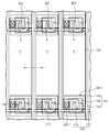
도 1은 본 발명의 제1 실시예에 따른 표시 기판을 개략적으로 나타낸 평면도이다.1 is a plan view schematically illustrating a display substrate according to a first exemplary embodiment of the present invention.
도 1을 참조하면, 본 발명의 일 실시예에 따른 표시 기판(100)은 실질적으로 영상을 표시하는 표시 영역(DA)과 표시 영역(DA)을 감싸는 비표시 영역(NDA)을 포함한다.Referring to FIG. 1, the
표시 영역(DA)에는 게이트 라인(122), 데이터 라인(142), 박막 트랜지스터(TFT) 및 스토리지 커패시터(Cst) 등이 형성된다. 비표시 영역(NDA)에는 게이트 라인(122)과 연결되는 게이트 패드부(GP) 및 데이터 라인(142)과 연결되는 데이터 패드부(DP)가 형성된다.In the display area DA, a
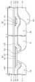
도 2는 도 1의 표시 영역의 일 부분을 확대하여 나타낸 확대도이며, 도 3는 도 2의 절단선 Ⅰ-Ⅰ` 및 절단선 Ⅱ-Ⅱ`을 따라 절단한 단면도이다.FIG. 2 is an enlarged view illustrating an enlarged portion of the display area of FIG. 1, and FIG. 3 is a cross-sectional view taken along the cutting line I-I ′ and the cutting line II-II ′ of FIG. 2.
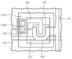
도 2 및 도 3을 참조하면, 표시 기판(100)은 베이스 기판(110) 상에 순차적으로 적층된 제1 금속 패턴(120), 제1 절연막(130), 제2 금속 패턴(140), 제2 절연막(150), 투명 전극(160), 유기막(170) 및 화소 전극(180)을 포함한다. 베이스 기판(110)은 예를 들어, 투명한 유리 또는 플라스틱으로 형성된다.2 and 3, the
제1 금속 패턴(120)은 베이스 기판(110) 상에 형성된다. 제1 금속 패턴(120)은 게이트 라인(122) 및 게이트 라인(122)으로부터 분기된 게이트 전극(124)을 포함할 수 있다. 게이트 라인(122)은 예를 들어, 가로 방향으로 연장된다. 게이트 전극(124)은 박막 트랜지스터(TFT)의 게이트 단자를 구성한다.The
제1 금속 패턴(120)은 예를 들어, 알루미늄(Al)과 몰리브덴(Mo)이 순차적으로 적층된 Mo/Al 2층막 구조로 형성된다. 이와 달리, 제1 금속 패턴(120)은 알루미늄(Al), 몰리브덴(Mo), 네오디뮴(Nd), 크롬(Cr), 탄탈륨(Ta), 티타늄(Ti), 텅스텐(W), 구리(Cu), 은(Ag) 등의 단일 금속 또는 이들의 합금이 1층 또는 복수의 층들로 형성될 수 있다.The
제1 절연막(130)은 제1 금속 패턴(120)이 형성된 기판(110) 상에 제1 금속 패턴(120)을 커버하도록 형성된다. 제1 절연막(130)은 제1 금속 패턴(120)을 보호하고 절연시키기 위한 절연막으로써, 예를 들어, 질화 실리콘(SiNx) 또는 산화 실리콘(SiOx)으로 형성되며, 약 1500Å ~ 2500Å의 두께로 형성된다.The first insulating
제2 금속 패턴(140)은 제1 절연막(130) 상에 형성된다. 제2 금속 패턴(140)은 데이터 라인(142), 데이터 라인(142)으로부터 분기된 소오스 전극(144) 및 소오 스 전극(144)과 이격된 드레인 전극(146)을 포함할 수 있다. 데이터 라인(142)은 제1 절연막(130)을 통해 게이트 라인(122)과 절연되며, 게이트 라인(122)과 교차되는 방향으로 연장되도록 형성된다. 예를 들어, 데이터 라인(142)은 게이트 라인(122)과 수직으로 교차되도록 세로 방향으로 연장된다. 소오스 전극(144)은 적어도 일부가 게이트 전극(124)과 중첩되도록 데이터 라인(142)으로부터 연장된다. 소오스 전극(144)은 박막 트랜지스터(TFT)의 소오스 단자를 구성한다. 드레인 전극(146)은 소오스 전극(144)과 소정의 간격으로 이격되게 형성되며, 일부가 게이트 전극(124)과 중첩되도록 형성된다. 드레인 전극(146)은 박막 트랜지스터(TFT)의 드레인 단자를 구성한다.The
제2 금속 패턴(140)은 예를 들어, 하부 몰리브덴층, 알루미늄층 및 상부 몰리브덴층이 연속적으로 적층된 Mo/Al/Mo 삼층막 구조로 형성된다. 이와 달리, 제2 금속 패턴(140)은 알루미늄(Al), 몰리브덴(Mo), 네오디뮴(Nd), 크롬(Cr), 탄탈륨(Ta), 티타늄(Ti), 텅스텐(W), 구리(Cu), 은(Ag) 등의 단일 금속 또는 이들의 합금이 1층 또는 복수의 층들로 형성될 수 있다.The
표시 기판(100)은 박막 트랜지스터(TFT)의 형성을 위하여, 제1 절연막(130)과 제2 금속 패턴(140) 사이에 형성되는 액티브 패턴(190)을 더 포함할 수 있다. 액티브 패턴(190) 및 제2 금속 패턴(140)은 마스크 공정 수를 감소시키기 위하여, 한 번의 마스크 공정을 통해 형성될 수 있다. 이와 같이, 한 번의 마스크 공정을 통해 액티브 패턴(190) 및 제2 금속 패턴(140)을 형성할 경우, 액티브 패턴(190)은 실질적으로 제2 금속 패턴(140)과 동일한 행태로 형성되며, 제1 절연막(130)과 제2 금속 패턴(140) 사이에 배치된다.The
한편, 액티브 패턴(190)을 형성하기 위한 마스크와 제2 금속 패턴(140)을 형성하기 위한 마스크를 달리 가져갈 경우, 액티브 패턴(190)은 게이트 전극(124)과 중첩되는 부분에만 형성될 수 있다.On the other hand, when the mask for forming the
액티브 패턴(190)은 반도체층(192) 및 오믹 콘택층(194)을 포함할 수 있다. 반도체층(192)은 실질적으로 전류가 흐르게 되는 채널 역할을 수행하며, 오믹 콘택층(194)은 반도체층(192)과 소오스 전극(144) 및 드레인 전극(146)간의 접촉 저항을 감소시키는 역할을 수행한다. 예를 들어, 반도체층(192)은 비정질 실리콘(amorphous Silicon : 이하, a-Si)으로 형성되며, 오믹 콘택층(194)은 n형 불순물이 고농도로 도핑된 비정질 실리콘(이하, n+a-Si)으로 형성된다.The
이에 따라, 표시 기판(100)의 각 화소(P) 내에는 게이트 전극(124), 액티브 패턴(190), 소오스 전극(144) 및 드레인 전극(146)을 포함하는 박막 트랜지스터(TFT)가 형성된다. 박막 트랜지스터(TFT)는 각 화소(P)를 개별적으로 구동시키기 위하여 각 화소(P)마다 적어도 하나가 형성된다. 박막 트랜지스터(TFT)는 게이트 라인(122)을 통해 인가되는 스캔 신호에 반응하여 데이터 라인(142)을 통해 인가되는 화소 전압을 화소 전극(180)에 인가한다.Accordingly, a thin film transistor TFT including a
제2 절연막(150)은 제2 금속 패턴(140)이 형성된 베이스 기판(110) 상에 제2 금속 패턴(140)을 커버하도록 형성된다. 제2 절연막(150)은 제2 금속 패턴(140)을 보호하고 절연시키기 위한 절연막으로서, 예를 들어, 질화 실리콘(SiNx) 또는 산화 실리콘(SiOx)으로 형성되며, 약 3500Å ~ 4500Å의 두께로 형성된다.The second
투명 전극(160)은 제2 절연막(150) 상에 형성된다. 투명 전극(160)은 유기막(170)을 사이에 두고 화소 전극(180)과 대향하여 스토리지 커패시터(Cst)를 형성한다. 박막 트랜지스터(TFT)를 통해 화소 전극(180)에 인가된 화소 전압은 스토리지 커패시터(Cst)에 의해 한 프레임 동안 유지된다. 투명 전극(160)에는 일정한 직류 전압이 인가된다. 예를 들어, 투명 전극(160)에는 스윙하는 화소 전압의 중간에 해당하는 직류 전압인 공통 전압(Vcom)이 인가된다.The
투명 전극(160)은 광이 투과될 수 있는 투명한 도전성 물질로 이루어진다. 예를 들어, 투명 전극(160)은 인듐 틴 옥사이드(Indium Tin Oxide : 이하, ITO) 또는 인듐 징크 옥사이드(Indium Zinc Oxide : 이하, IZO)로 형성된다. 투명 전극(160)은 예를 들어, 약 500Å ~ 600Å의 두께로 형성된다.The
제2 절연막(150) 및 투명 전극(160)에는 드레인 전극(146)과 화소 전극(180)간의 전기적인 연결을 위하여, 드레인 전극(146)의 적어도 일부를 노출시키는 제1 콘택 홀(CNT1)이 형성된다. 예를 들어, 제1 콘택 홀(CNT1)은 박막 트랜지스터(TFT) 상부에 위치하는 투명 전극(160)이 플로팅 상태를 가질 수 있도록 박막 트랜지스터(TFT) 부분을 둘러싸도록 형성된다. 이 경우, 상기 박막 트랜지스터(TFT)의 상부에 형성된 투명전극(160)에는 DC전압이 인가되지 않는다.In the second insulating
유기막(170)은 투명 전극(160) 상에 형성된다. 유기막(170)은 표시 기판(100)의 평탄화를 위하여 사용된다. 유기막(170)은 예를 들어, 약 2.5㎛ ~ 3.5㎛의 두께로 형성된다.The
유기막(170)은 적색, 녹색 및 청색 컬러필터들(RCF, GCF, BCF)을 포함할 수 있다. 적색, 녹색 및 청색 컬러필터들(RCF, GCF, BCF)은 각 화소(P)에 대응하여 순차적으로 배열된다. 바람직하게, 적색, 녹색 및 청색 컬러필터들(RCF, GCF, BCF)은 데이터 라인(142) 상에서 서로 중첩되도록 형성된다. 이와 같이, 적색, 녹색 및 청색 컬러필터들(RCF, GCF, BCF) 중에서 적어도 둘 이상을 중첩시킬 경우, 데이터 라인(142) 근처에서 발생되는 빛샘이 방지되어 대향 기판에 형성되는 블랙 매트릭스의 폭을 데이터 라인(142)의 선폭 만큼 최소로 감소시킬 수 있어, 개구율을 증가시킬 수 있다.The
유기막(170)에는 드레인 전극(146)과 화소 전극(180)간의 전기적인 연결을 위하여, 드레인 전극(146)의 적어도 일부를 노출시키는 제2 콘택 홀(CNT2)이 형성된다. 제2 콘택 홀(CNT2)은 제1 콘택 홀(CNT1) 내에 형성된다.In the
유기막(170)은 제1 콘택 홀(CNT1)에 대응되는 제2 절연막(150) 및 투명 전극(160)의 식각 단면을 커버한다. 따라서, 유기막(170)은 제1 콘택 홀(CNT1) 영역에서 투명 전극(160)과 화소 전극(180)이 단락되는 것을 방지한다.The
화소 전극(180)은 각 화소(P)에 대응하여 유기막(170) 상에 형성된다. 화소 전극(180)은 광이 투과될 수 있는 투명한 도전성 물질로 이루어진다. 예를 들어, 화소 전극(180)은 인듐 틴 옥사이드(Indium Tin Oxide : 이하, ITO) 또는 인듐 징크 옥사이드(Indium Zinc Oxide : 이하, IZO)로 형성된다.The
화소 전극(180)은 유기막(170)에 형성된 제2 콘택 홀(CNT2)을 통해 드레인 전극(146)과 전기적으로 연결된다. 따라서, 게이트 라인(122)을 통해 박막 트랜지스터(TFT)의 게이트 전극(124)에 스캔 신호가 인가되면, 박막 트랜지스터(TFT)가 턴-온(turn on)되어 데이터 라인(142)을 통해 박막 트랜지스터(TFT)의 소오스 전극(144)으로 인가된 화소 전압이 드레인 전극(146)을 거쳐 화소 전극(180)에 인가된다.The
화소 전극(180)은 투명 전극(160)과 전체적으로 중첩되어 스토리지 커패시터(Cst)를 형성한다. 박막 트랜지스터(TFT)의 구동을 통해 화소 전극(180)에 인가된 화소 전압은 스토리지 커패시터(Cst)를 통해 한 프레임동안 유지된다.The
한편, 상기 화소 전극(180)의 가장자리는 상기 데이터 라인(142)과 중첩될 수 있다. 또한, 상기 화소 전극(180)은 광시야각의 구현을 위하여 각 화소(P)를 다수의 도메인으로 분할하기 위한 특정한 개구 패턴을 가질 수 있다.The edge of the
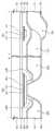
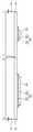
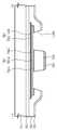
도 4는 도 1의 게이트 패드부를 나타낸 확대도이며, 도 5는 도 4의 Ⅲ-Ⅲ'선을 따라 절단한 단면도이다.4 is an enlarged view illustrating the gate pad part of FIG. 1, and FIG. 5 is a cross-sectional view taken along line III-III ′ of FIG. 4.
도 1, 도 4 및 도 5을 참조하면, 표시 기판(100)의 비표시 영역(NDA)은 패드 영역(PA) 및 패드 영역(PA)과 표시 영역(DA)의 사이인 팬 아웃 영역(FA)을 포함한다. 패드 영역(PA)에는 게이트 패드부(GP) 및 데이터 패드부(DP)가 형성된다. 팬 아웃 영역(FA)에는 게이트 라인(122)과 게이트 패드부(GP)를 연결하고, 데이터 라인(142)과 데이터 패드부(DP)를 연결하는 팬 아웃 라인(230)이 형성된다.1, 4, and 5, the non-display area NDA of the
게이트 패드부(GP)는 게이트 금속 패드(210) 및 게이트 투명 패드(220)를 포함한다.The gate pad part GP includes a
게이트 금속 패드(210)는 게이트 라인(122)과 연결되며, 표시 영역(DA)의 외곽인 비표시 영역(NDA) 중 패드 영역(PA)에 형성된다. 게이트 금속 패드(210)는 베이스 기판(110) 상에 제1 금속 패턴(120)과 동일한 물질로 형성되며, 제1 금속 패턴(120)을 형성할 때 동시에 형성된다.The
게이트 투명 패드(220)는 게이트 금속 패드(210) 상에 형성되어 게이트 금속 패드(210)와 직접 접촉된다. 게이트 투명 패드(220)는 게이트 금속 패드(210)의 폭 방향의 양단부를 커버하도록 게이트 금속 패드(210)보다 넓은 폭으로 형성된다. 게이트 투명 패드(220)는 예를 들어, 화소 전극(190)과 동일한 물질로 형성되며, 화소 전극(180)을 형성할 때 동시에 형성된다.The gate
제1 절연막(130), 제2 절연막(150) 및 투명 전극(160)에는 게이트 금속 패드(210)와 게이트 투명 패드(220)의 연결을 위하여, 게이트 금속 패드(210)를 노출시키는 제3 콘택 홀(CNT3)이 형성된다.A third contact exposing the
투명 전극(160)과 게이트 투명 전극(220)은 도전성 물질을 포함하므로, 투명 전극(160)과 게이트 투명 전극(220)이 접촉되지 않도록 제3 콘택 홀(CNT3)은 게이트 투명 전극(220)보다 넓은 면적으로 형성된다.Since the
유기막(170)은 표시 영역(DA)으로부터 연장되어 팬 아웃 영역(FA)에 인접한 패드 영역(PA)의 단부까지 형성된다. 유기막(170)은 팬 아웃 영역(FA)에 인접한 제3 콘택 홀(CNT3)의 식각 단면을 커버한다. 따라서, 팬 아웃 영역(FA)에 인접한 게이트 투명 패드(220)의 길이 방향의 일단부는 유기막(170)에 의해 투명 전극(160)과 확실히 절연될 수 있다.The
데이터 패드부(DP) 제1 절연막(130) 상에 데이터 금속 패드 및 데이터 투명 패드가 형성되는 것을 제외하고는 실질적으로 게이트 패드부(GP)와 유사한 구조를 가지므로, 이에 대한 상세한 설명은 생략하기로 한다.The data pad part DP has a structure substantially similar to that of the gate pad part GP except that a data metal pad and a data transparent pad are formed on the first insulating
한편, 도시되지는 않았으나, 게이트 패드부(GP) 및 데이터 패드부(DP)가 형성된 패드 영역(PA)의 투명 전극(160) 및 제2 절연막(150)을 전면적으로 제거함으로써, 투명 전극(160)과 게이트 투명 전극(220) 및 데이터 투명 전극간의 단락을 방지할 수 있다.Although not shown, the
상기 본 발명의 제1실시예와 같이, 화소 전극(180)과 대향하여 스토리지 커패시터(Cst)를 형성하는 전극을 금속이 아닌 투명 전극(160)으로 형성함으로써, 개구율을 최대로 증가시킬 수 있다.As in the first embodiment of the present invention, by forming the electrode forming the storage capacitor Cst opposite the
또한, 유기막(170)을 사이에 두고 화소 전극(180)과 투명 전극(160)이 동일 면적으로 중첩되면, 스토리지 커패시터(Cst)의 커패시턴스가 확대되어 RGB 감마처짐 및 플리커 등이 개선되고, 킥-백(kick-back)이 최소화된다.In addition, when the
또한, 화소 전극(180)과 데이터 라인(142) 사이에 일정한 직류 전압이 인가되는 투명 전극(160)이 존재하므로, 화소 전극(180)과 데이터 라인(142)간에 발생되는 기생 커패시터가 최소화되고, 이에 따라, 화소 전극(180)과 데이터 라인(142)간의 얼라인 미스로 인한 커패시터의 편차로 인해 발생되는 세로줄 얼룩 등의 불량을 방지할 수 있다.In addition, since there is a
또한, 데이터 라인(142) 상에 투명 전극(160)이 존재함으로 인해, 데이터 라인(142)과 대향 기판의 공통 전극간의 기생 커패시터 및 데이터 라인(142)과 화소 전극(180)간의 기생 커패시터를 최소화되어 데이터 라인(142)에 걸리는 부하가 감소되며, 이에 따라, 데이터 라인(142)을 흐르는 화소 전압의 지연이 감소된다.In addition, the presence of the
또한, 데이터 라인(142) 상에 배치된 투명 전극(160)이 스윙하는 화소 전압이 흐르는 데이터 라인(142)과 공통 전압(Vcom)이 인가되는 대향 기판의 공통 전극간에 발생되는 커플링을 방지하여, 초록 빛을 띠는 그리니쉬(greenish) 현상이 개선된다.In addition, the
이하에서는, 본 발명의 제2실시예에 따른 표시기판에 대하여 도6 및 도7을 참조하여 설명한다. 본 실시예에 있어서, 상기한 제1 실시예와 중복되는 요소에 대하여는 자세한 설명을 생략하며, 상기 제1실시예와의 차이점을 중심으로 설명한다.Hereinafter, a display substrate according to a second exemplary embodiment of the present invention will be described with reference to FIGS. 6 and 7. In the present embodiment, detailed descriptions of elements overlapping with the above-described first embodiment will be omitted, and the description will be mainly focused on differences from the first embodiment.
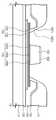
도 6은 본 발명의 다른 실시예에 따른 표시 기판을 나타낸 확대도이며, 도 7는 도 6의 Ⅳ-Ⅳ'선을 따라 절단한 단면도이다.6 is an enlarged view illustrating a display substrate according to another exemplary embodiment. FIG. 7 is a cross-sectional view taken along line IV-IV ′ of FIG. 6.
도 6 및 도 7을 참조하면, 표시 기판(100)은 더미 절연막(152) 및 더미 투명 전극(162)을 더 포함할 수 있다.6 and 7, the
더미 절연막(152)은 제2 콘택 홀(CNT2)에 의해 노출된 드레인 전극(146) 상에 적어도 하나 이상이 형성된다. 더미 절연막(152)은 제2 콘택 홀(CNT2) 내에서 유기막(170)과 이격되도록 섬 형태로 형성된다. 더미 절연막(152)은 제2 절연막(150)과 동일한 물질로 동시에 형성될 수 있다.At least one
앞서 설명한 바와 같이, 드레인 전극(146)을 포함하는 제2 금속 패턴(140)은 제1 절연막(130)으로부터 순차적으로 형성된 하부 몰리브덴층(140a), 알루미늄층(140b) 및 상부 몰리브덴층(140c)을 포함한다.As described above, the
제1 콘택 홀(CNT1) 내에서 더미 절연막(152)이 형성된 영역을 제외한 나머지 영역의 상부 몰리브덴층(140c)은 제거되어 있다. 따라서, 화소 전극(180)은 더미 절연막(152)의 하부에 잔존하는 상부 몰리브덴층(140c)과 측면 접촉(side contact)하게 되며, 드레인 전극(146)과 화소 전극(180)간의 접촉 신뢰성이 향상된다. 상기 상부 몰리브덴층(140c)의 제거는, 제1 콘택 홀(CNT1)을 형성하기 위하여 제2 절연막(150)을 건식 식각할 때, 과잉 식각을 통해 이루어질 수 있다.The
이하에서는 본 발명의 제3 실시예에 따른 표시기판에 대하여 도8 및 도9를 참조하여 설명한다. 본 실시예에 있어서, 상기한 제1 및 제2 실시예와 중복되는 요소에 대하여는 자세한 설명을 생략하며, 상기 제1, 제2 실시예와의 차이점을 중심으로 설명한다.Hereinafter, a display substrate according to a third exemplary embodiment of the present invention will be described with reference to FIGS. 8 and 9. In the present embodiment, detailed descriptions of elements overlapping with the above-described first and second embodiments will be omitted, and description will be made focusing on differences from the first and second embodiments.
도 8A는 본 발명의 제3 실시예에 따른 표시 기판의 일 부분을 확대하여 나타낸 확대도이며, 도 8B는 도 8A에 도시된 절단선 VII-VII`에 따라 절단한 단면도이다.8A is an enlarged view illustrating a portion of a display substrate according to a third exemplary embodiment of the present invention, and FIG. 8B is a cross-sectional view taken along the cutting line VII-VII ′ of FIG. 8A.
도 8A 및 도 8B를 참조하면, 상기 투명전극(160)은 상기 제1 콘택 홀(CNT1)이 형성된 영역을 제외한 상기 베이스 기판(110) 상에 형성된 각 픽셀(P)의 전체영역을 커버하도록 형성된다. 상기 제1 콘택 홀(CNT1)은 드레인 전극(146)이 형성된 영역 내에서 드레인 전극(146)을 부분적으로 노출시키도록 형성된다. 따라서, 상기 투명전극(160)은 상기 제1 콘택 홀(CNT1)이 형성된 상기 드레인 전극(146)의 일부 영역을 제외하고는, 상기 게이트 라인(122), 데이터 라인(142) 및 상기 액티브 패턴(190) 등을 포함한 상기 픽셀(P)의 전체 영역을 커버한다.8A and 8B, the
상기한 바와 같이, 제1 콘택 홀(CNT1)이 상기 드레인 전극(146)이 구비된 영역 내에 형성되므로, 상기 제1 콘택 홀(CNT1)을 형성하기 위하여 상기 제2 절연 막(150)을 건식 식각하는 과정 상에서 발생될 수 있는 상기 게이트 라인(122) 및 상기 데이터 라인(142)의 손상을 방지할 수 있다.As described above, since the first contact hole CNT1 is formed in the region provided with the
한편, 유기막(170)에는 제2 콘택 홀(CNT2)이 제공되고, 상기 제2 콘택 홀(CNT2)은 제1 콘택 홀(CNT1)보다 작은 크기로 제1 콘택 홀(CNT1) 내에 형성된다.Meanwhile, a second contact hole CNT2 is provided in the
상기 제1 실시예에서 설명한 바와 같이, 상기 투명전극(160)에는 DC전압(Vt)이 인가된다. 다만, 상기 제1 실시예에서와는 달리, 상기 액티브 패턴(190) 상부의 투명전극(160)에도 동일한 DC전압(Vt)이 인가될 수 있는바, 이는 상기 투명전극(160)이 상기 제1 콘택 홀(CNT1)이 형성된 상기 드레인 전극(146)의 일부 영역을 제외하고는 상기 픽셀(P) 상에 연속적으로 형성되기 때문이다.As described in the first embodiment, a DC voltage Vt is applied to the
도 9는 도 8A에 도시된 투명전극에 인가되는 DC전압의 레벨에 따라 TFT의 문턱 전압과 전류 관계를 나타낸 그래프이다.FIG. 9 is a graph illustrating a relationship between a threshold voltage and a current of a TFT according to a level of a DC voltage applied to the transparent electrode illustrated in FIG. 8A.
도 9에 도시된 것처럼, 상기 DC전압(Vt)의 레벨을 변화시킴으로써 상기 박막 트랜지스터(TFT)의 문턱전압(Vth)을 조절할 수 있다. 즉, 도 9에서는 상기 투명전극(160)에 인가되는 DC전압(Vt)을 증가시킬수록 상기 박막 트랜지스터(TFT)의 문턱전압(Vth)이 감소되는 것으로 나타났다. 여기서, 상기 DC전압(Vt)이 증가될수록 상기 액티브 패턴(190)에서 전자가 더 많이 축적되므로 상기 박막 트랜지스터(TFT)의 구동을 위한 문턱전압(Vth)은 낮아지게 되는 것이다.As illustrated in FIG. 9, the threshold voltage Vth of the thin film transistor TFT may be adjusted by changing the level of the DC voltage Vt. That is, in FIG. 9, as the DC voltage Vt applied to the
이하에서는, 본 발명의 일 실시예에 따른 표시 기판의 제조 방법에 대하여 설명한다.Hereinafter, a method of manufacturing a display substrate according to an exemplary embodiment of the present invention will be described.
도 10 내지 도 17은 도 2 및 도 3에 도시된 표시 기판의 제조 과정을 설명하 기 위한 도면들이다.10 to 17 are diagrams for describing a manufacturing process of the display substrate illustrated in FIGS. 2 and 3.
도 10 및 도 11을 참조하면, 베이스 기판(110) 상에 제1 금속 패턴(120)을 형성한다. 제1 금속 패턴(120)은 게이트 라인(122) 및 게이트 라인(122)으로부터 분기된 게이트 전극(124)을 포함한다.10 and 11, the
제1 금속 패턴(120)은 예를 들어, 알루미늄층과 몰리브덴층이 순차적으로 적층된 Mo/Al 2층막 구조를 갖는다. 이와 달리, 제1 금속 패턴(120)은 알루미늄(Al), 몰리브덴(Mo), 네오디뮴(Nd), 크롬(Cr), 탄탈륨(Ta), 티타늄(Ti), 텅스텐(W), 구리(Cu), 은(Ag) 등의 단일 금속 또는 이들의 합금이 1층 또는 복수의 층들로 형성될 수 있다.The
도 12 및 도 13을 참조하면, 제1 금속 패턴(120)이 형성된 베이스 기판(110) 상에 제1 금속 패턴(120)을 커버하도록 제1 절연막(130)을 형성한다. 예를 들어, 제1 절연막(130)은 질화 실리콘(SiNx) 또는 산화 실리콘(SiOx)으로 형성되며, 약 1500Å ~ 2500Å의 두께로 형성된다.12 and 13, a first insulating
제1 절연막(130) 상에 액티브 패턴(190) 및 제2 금속 패턴(140)을 형성한다. 액티브 패턴(190) 및 제2 금속 패턴(140)은 서로 다른 2개의 마스크를 이용한 2번의 마스크 공정을 통해 각각 패터닝되거나, 또는 하나의 마스크를 이용한 한번의 마스크 공정을 통해 패터닝될 수 있다. 예를 들어, 액티브 패턴(190)과 제2 금속 패턴(140)을 2번의 마스크 공정을 통해 각각 패터닝할 경우, 액티브 패턴(190)은 게이트 전극(124)과 중첩되는 부분에만 형성될 수 있다. 이와 달리, 액티브 패턴(190)과 제2 금속 패턴(140)이 한 번의 마스크 공정에 의해 패터닝될 경우, 액티 브 패턴(190)은 실질적으로 제2 금속 패턴(140)과 동일한 형상으로 형성된다. 즉, 액티브 패턴(190)은 제1 절연막(130)과 제2 금속 패턴(140) 사이에 형성된다.The
액티브 패턴(190)은 반도체층(192) 및 오믹 콘택층(194)을 포함할 수 있다. 예를 들어, 반도체층(192)은 비정질 실리콘(amorphous Silicon : a-Si)으로 형성되며, 오믹 콘택층(194)은 n형 불순물이 고농도로 도핑된 비정질 실리콘(n+a-Si)으로 형성된다.The
제2 금속 패턴(140)은 게이트 라인(122)과 교차하는 데이터 라인(142), 데이터 라인(142)으로부터 분기된 소오스 전극(144) 및 소오스 전극(144)과 이격된 드레인 전극(146)을 포함한다.The
제2 금속 패턴(140)은 예를 들어, 하부 몰리브덴층, 알루미늄층 및 상부 몰리브덴층이 연속적으로 적층된 Mo/Al/Mo 삼층막 구조로 형성된다. 이와 달리, 제2 금속 패턴(140)은 알루미늄(Al), 몰리브덴(Mo), 네오디뮴(Nd), 크롬(Cr), 탄탈륨(Ta), 티타늄(Ti), 텅스텐(W), 구리(Cu), 은(Ag) 등의 단일 금속 또는 이들의 합금이 1층 또는 복수의 층들로 형성될 수 있다.The
한편, 박막 트랜지스터(TFT)의 형성을 위하여 소오스 전극(144)과 드레인 전극(146) 사이에 해당하는 채널 영역의 오믹 콘택층(194)은 제거된다.Meanwhile, the
도 14 및 도 15을 참조하면, 제2 금속 패턴(140)이 형성된 베이스 기판(110) 상에 제2 금속 패턴(140)을 커버하도록 제2 절연막(150) 및 투명 전극(160)을 순차적으로 형성한다.14 and 15, the second insulating
제2 절연막(150)은 예를 들어, 질화 실리콘(SiNx) 또는 산화 실리콘(SiOx)으 로 형성되며, 약 3500Å ~ 4500Å의 두께로 형성된다. 투명 전극(160)은 광이 투과될 수 있는 투명한 도전성 물질로 이루어진다. 예를 들어, 투명 전극(160)은 인듐 틴 옥사이드(Indium Tin Oxide : 이하, ITO) 또는 인듐 징크 옥사이드(Indium Zinc Oxide : 이하, IZO)로 형성되며, 약 500Å ~ 600Å의 두께로 형성된다.The second
제2 절연막(150) 및 투명 전극(160)에 드레인 전극(146)의 적어도 일부를 노출시키는 제1 콘택 홀(CNT1)을 형성한다. 예를 들어, 제1 콘택 홀(CNT1)은 한번의 마스크 공정을 통해 형성될 수 있다. 제1 콘택 홀(CNT1) 영역의 투명 전극(160)은 습식 식각에 의해 제거되고, 제1 콘택 홀(CNT1) 영역의 제2 절연막(150)은 건식 식각에 의해 제거될 수 있다.A first contact hole CNT1 exposing at least a portion of the
도 16 및 도 17을 참조하면, 제1 콘택 홀(CNT1)이 형성된 투명 전극(160) 상에 유기막(170)을 형성한다. 유기막(170)은 표시 기판(100)의 평탄화를 위하여 사용된다. 유기막(170)은 예를 들어, 약 2.5㎛ ~ 3.5㎛의 두께로 형성된다.16 and 17, the
유기막(170)은 적색, 녹색 및 청색 컬러필터들(RCF, GCF, BCF)을 포함할 수 있다. 적색, 녹색 및 청색 컬러필터들(RCF, GCF, BCF)은 각 화소(P)에 대응하여 순차적으로 배열된다. 적색, 녹색 및 청색 컬러필터들(RCF, GCF, BCF)은 빛샘을 방지하기 위하여 데이터 라인(142) 상에서 서로 중첩되도록 형성되는 것이 바람직하다.The
유기막(170)에 드레인 전극(146)의 적어도 일부를 노출시키는 제2 콘택 홀(CNT2)을 형성한다. 유기막(170)이 제1 콘택 홀(CNT1)에 대응되는 제2 절연막(150) 및 투명 전극(160)의 식각 단면을 커버하도록 제2 콘택 홀(CNT2)은 제1 콘 택 홀(CNT1) 내에 형성된다. 따라서, 유기막(170)은 제1 콘택 홀(CNT1) 영역에서 투명 전극(160)과 화소 전극(180)이 접촉되는 것을 방지한다.A second contact hole CNT2 exposing at least a portion of the
다시 도 2 및 도 3을 참조하면, 제2 콘택 홀(CNT2)이 형성된 유기막(170) 상에 각 화소(P)에 대응되도록 화소 전극(180)을 형성한다. 화소 전극(180)은 광이 투과될 수 있는 투명한 도전성 물질로 이루어진다. 예를 들어, 화소 전극(180)은 인듐 틴 옥사이드(Indium Tin Oxide : 이하, ITO) 또는 인듐 징크 옥사이드(Indium Zinc Oxide : 이하, IZO)로 형성되며, 약 500Å ~ 600Å의 두께로 형성된다.2 and 3, the
화소 전극(180)은 유기막(170)에 형성된 제2 콘택 홀(CNT2)을 통해 드레인 전극(146)과 전기적으로 연결된다. 이때, 유기막(170)이 제1 콘택 홀(CNT1)의 식각 단면을 커버하고 있기 때문에, 화소 전극(180)과 투명 전극(160)은 접촉되지 않는다. 화소 전극(180)은 투명 전극(160)과 전체적으로 중첩되어 스토리지 커패시터(Cst)를 형성한다.The
도 18 내지 도 21은 도 6 및 도 7에 도시된 표시 기판의 제조 과정을 설명하기 위한 도면들이다. 도 18 및 도 21에서, 제2 금속 패턴을 형성하는 공정까지는 도 10 내지 도 13에 도시된 것과 동일하므로, 이와 관련된 중복되는 상세한 설명은 생략하기로 한다.18 to 21 are diagrams for describing a manufacturing process of the display substrate illustrated in FIGS. 6 and 7. In FIGS. 18 and 21, the processes up to the process of forming the second metal pattern are the same as those illustrated in FIGS. 10 to 13, and thus detailed descriptions thereof will be omitted.
도 18 및 도 19를 참조하면, 제2 금속 패턴(140)이 형성된 베이스 기판(110) 상에 제2 금속 패턴(140)을 커버하도록 제2 절연막(150) 및 투명 전극(160)을 순차적으로 형성한다.18 and 19, the second insulating
제2 절연막(150) 및 투명 전극(160)에 드레인 전극(146)의 적어도 일부를 노 출시키는 제1 콘택 홀(CNT1)을 형성한다. 이때, 제1 콘택 홀(CNT1)에 의해 노출되는 드레인 전극(146) 상에는 더미 절연막(152) 및 더미 투명 전극(162)이 형성된다. 더미 절연막(152)은 제2 절연막(150)과 동일한 물질로 형성되며, 더미 투명 전극(162)은 투명 전극(160)과 동일한 물질로 형성된다.A first contact hole CNT1 exposing at least a portion of the
제1 콘택 홀(CNT1)은 한번의 마스크 공정을 통해 형성된다. 제1 콘택 홀(CNT1) 영역의 투명 전극(160)은 습식 식각 공정에 의해 제거되고, 제1 콘택 홀(CNT1) 영역의 제2 절연막(150)은 건식 식각 공정에 의해 제거된다. 본 실시예에서는, 제2 절연막(150)을 건식 식각할 때, 과잉 식각(over etch)을 통해 제1 콘택 홀(CNT1)에 의해 노출된 드레인 전극(146)의 상부 몰리브덴층(140c)을 같이 제거한다.The first contact hole CNT1 is formed through one mask process. The
도 20 및 도 21을 참조하면, 제1 콘택 홀(CNT1)이 형성된 투명 전극(160) 상에 컬러필터들을 포함할 수 있는 유기막(170)을 형성한 후, 유기막(170)에 드레인 전극(146)의 적어도 일부를 노출시키는 제2 콘택 홀(CNT2)을 형성한다. 유기막(170)은 제1 콘택 홀(CNT1) 영역에서 투명 전극(160)과 화소 전극(180)이 접촉되는 것을 방지하기 위하여, 제1 콘택 홀(CNT1)에 대응되는 제2 절연막(150) 및 투명 전극(160)의 식각 단면을 커버한다.20 and 21, after forming the
다시 도 6 및 도 7을 참조하면, 제2 콘택 홀(CNT2)이 형성된 유기막(170) 상에 각 화소(P)에 대응되도록 화소 전극(180)을 형성한다. 제2 콘택 홀(CNT2) 내에서 더미 절연막(152) 및 더미 투명 전극(162)이 형성된 영역을 제외한 나머지 영역의 상부 몰리브덴층(140c)은 제거되어 있으므로, 화소 전극(180)은 더미 절연 막(152)의 하부에 잔존하는 상부 몰리브덴층(140c)과 측면 접촉(side contact)하게 된다. 따라서, 드레인 전극(146)과 화소 전극(180)간의 접촉 신뢰성이 향상된다.6 and 7, the
이하에서는 본 발명에 따른 표시 장치에 대하여 설명한다. 여기서, 표시 기판(100)은 도 1 내지 도 19에 도시된 실시예들과 동일한 구조를 가질 수 있으므로, 이와 관련된 상세한 설명은 생략하기로 한다. 여기에서는 상기한 표시장치의 실시예들 중 제1 실시예의 구조를 갖는 표시기판이 장착된 표시장치에 대하여 설명한다.Hereinafter, a display device according to the present invention will be described. Here, since the
도 22는 본 발명의 일 실시예에 따른 표시 장치를 나타낸 단면도이다.22 is a cross-sectional view illustrating a display device according to an exemplary embodiment.
도 22를 참조하면, 표시 장치(300)는 표시 기판(100), 대향 기판(400) 및 액정층(500)을 포함한다.Referring to FIG. 22, the
대향 기판(400)은 액정층(500)을 사이에 두고 표시 기판(100)과 대향하도록 배치된다. 대향 기판(400)은 표시 기판(100)과 대향하는 기판(410)의 대향면에 형성된 공통 전극(420)을 포함할 수 있다. 공통 전극(420)은 광의 투과를 위하여 투명한 도전성 물질로 형성된다. 예를 들어, 공통 전극(420)은 화소 전극(180)과 동일한 인듐 징크 옥사이드(Indium Zinc Oxide : IZO) 또는 인듐 틴 옥사이드(Indium Tin Oxide : ITO)로 형성된다. 공통 전극(420)에는 광시야각의 구현을 위한 개구 패턴이 형성될 수 있다.The
대향 기판(400)은 블랙 매트릭스(430)를 더 포함할 수 있다. 블랙 매트릭스(430)는 화소(P)들의 경계부에 형성되어 빛샘을 차단하고 대비비(contrast ratio)를 향상시킨다. 표시 기판(100)에 형성된 적색, 녹색 및 청색 컬러필터 들(RCF, GCF, BCF)를 중첩시킴으로써, 블랙 매트릭스(430)의 폭을 감소시키고 개구율을 증가시킬 수 있다.The
한편, 표시 기판(100)에 컬러필터들이 형성되지 않은 경우, 대향 기판(400)은 컬러필터들을 포함할 수 있다.If no color filters are formed on the
액정층(500)은 이방성 굴절률, 이방성 유전율 등의 광학적, 전기적 특성을 갖는 액정들이 일정한 형태로 배열된 구조를 갖는다. 액정층(500)은 화소 전극(180)과 공통 전극(420) 사이에 형성되는 전계에 의하여 액정들의 배열이 변화되고, 액정들의 배열 변화에 따라서 통과하는 광의 투과율을 제어한다.The
앞서 설명한 본 발명의 상세한 설명에서는 본 발명의 바람직한 실시예들을 참조하여 설명하였지만, 해당 기술분야의 숙련된 당업자 또는 해당 기술분야에 통상의 지식을 갖는 자라면 후술될 특허청구범위에 기재된 본 발명의 사상 및 기술 영역으로부터 벗어나지 않는 범위 내에서 본 발명을 다양하게 수정 및 변경시킬 수 있음을 이해할 수 있을 것이다.While the present invention has been described in connection with what is presently considered to be practical and exemplary embodiments, it is to be understood that the invention is not limited to the disclosed embodiments, but, on the contrary, It will be understood by those skilled in the art that various changes in form and details may be made therein without departing from the spirit and scope of the invention as defined by the appended claims.
도 1은 본 발명의 제1 실시예에 따른 표시 기판을 개략적으로 나타낸 평면도이다.1 is a plan view schematically illustrating a display substrate according to a first exemplary embodiment of the present invention.
도 2는 도 1의 표시 영역을 나타낸 확대도이다.FIG. 2 is an enlarged view of the display area of FIG. 1.
도 3는 도 2의 Ⅰ-Ⅰ'선 및 Ⅱ-Ⅱ'선을 따라 절단한 단면도이다.3 is a cross-sectional view taken along lines II ′ and II-II ′ of FIG. 2.
도 4는 도 1의 게이트 패드부를 나타낸 확대도이다.4 is an enlarged view illustrating the gate pad part of FIG. 1.
도 5는 도 4의 Ⅲ-Ⅲ'선을 따라 절단한 단면도이다.FIG. 5 is a cross-sectional view taken along line III-III ′ of FIG. 4.
도 6는 본 발명의 제2 실시예에 따른 표시 기판을 나타낸 확대도이다.6 is an enlarged view illustrating a display substrate according to a second exemplary embodiment of the present invention.
도 7은 도 6의 Ⅳ-Ⅳ'선을 따라 절단한 단면도이다.FIG. 7 is a cross-sectional view taken along line IV-IV ′ of FIG. 6.
도 8A는 본 발명의 제3 실시예에 따른 표시 기판의 일 부분을 확대하여 나타낸 확대도이다.8A is an enlarged view illustrating a portion of a display substrate according to a third exemplary embodiment of the present invention.
도 8B는 도 8A에 도시된 절단선 Ⅶ-Ⅶ'에 따라 절단한 단면도이다.FIG. 8B is a cross-sectional view taken along the cutting line VIII-VIII 'shown in FIG. 8A.
도 9는 도 8A에 도시된 투명전극에 인가되는 DC전압의 레벨에 따라 TFT의 문턱 전압과 전류 관계를 나타낸 그래프이다.FIG. 9 is a graph illustrating a relationship between a threshold voltage and a current of a TFT according to a level of a DC voltage applied to the transparent electrode illustrated in FIG. 8A.
도 10 내지 도 17은 도 2 및 도 3에 도시된 표시 기판의 제조 과정을 설명하기 위한 도면들이다.10 to 17 are diagrams for describing a manufacturing process of the display substrate illustrated in FIGS. 2 and 3.
도 18 내지 도 21은 도 6 및 도 7에 도시된 표시 기판의 제조 과정을 설명하기 위한 도면들이다.18 to 21 are diagrams for describing a manufacturing process of the display substrate illustrated in FIGS. 6 and 7.
도 22는 본 발명의 일 실시예에 따른 표시 장치를 나타낸 단면도이다.22 is a cross-sectional view illustrating a display device according to an exemplary embodiment.
<도면의 주요 부분에 대한 부호의 설명><Explanation of symbols for the main parts of the drawings>
100 : 표시 기판120 : 제1 금속 패턴100: display substrate 120: first metal pattern
122 : 게이트 라인124 : 게이트 전극122: gate line 124: gate electrode
130 : 제1 절연막140 : 제2 금속 패턴130: first insulating film 140: second metal pattern
142 : 데이터 라인144 : 소오스 전극142: data line 144: source electrode
146 : 드레인 전극150 : 제2 절연막146: drain electrode 150: second insulating film
160 : 투명 전극170 : 유기막160: transparent electrode 170: organic film
180 : 화소 전극190 : 액티브 패턴180
300 : 표시 장치400 : 대향 기판300: display device 400: opposing substrate
420 : 공통 전극430 : 블랙 매트릭스420: common electrode 430: black matrix
500 : 액정층500: liquid crystal layer
Claims (25)
Translated fromKoreanPriority Applications (1)
| Application Number | Priority Date | Filing Date | Title |
|---|---|---|---|
| US12/129,198US8111342B2 (en) | 2007-05-30 | 2008-05-29 | Display substrate, method of manufacturing the same and display device using the display substrate |
Applications Claiming Priority (2)
| Application Number | Priority Date | Filing Date | Title |
|---|---|---|---|
| KR20070052453 | 2007-05-30 | ||
| KR1020070052453 | 2007-05-30 |
Publications (2)
| Publication Number | Publication Date |
|---|---|
| KR20080105973A KR20080105973A (en) | 2008-12-04 |
| KR101376754B1true KR101376754B1 (en) | 2014-03-26 |
Family
ID=40367157
Family Applications (1)
| Application Number | Title | Priority Date | Filing Date |
|---|---|---|---|
| KR1020080007983AActiveKR101376754B1 (en) | 2007-05-30 | 2008-01-25 | Display substrate, method of manufacturing the same and display apparatus having the same |
Country Status (1)
| Country | Link |
|---|---|
| KR (1) | KR101376754B1 (en) |
Citations (2)
| Publication number | Priority date | Publication date | Assignee | Title |
|---|---|---|---|---|
| US6697138B2 (en) | 2001-02-22 | 2004-02-24 | Lg Phillips Lcd Co., Ltd. | Transflective liquid crystal display device and manufacturing method for the same |
| US7133105B2 (en) | 2002-12-09 | 2006-11-07 | Lg.Philips Lcd Co., Ltd. | Array substrate for liquid crystal display device and method of fabricating the same |
- 2008
- 2008-01-25KRKR1020080007983Apatent/KR101376754B1/enactiveActive
Patent Citations (2)
| Publication number | Priority date | Publication date | Assignee | Title |
|---|---|---|---|---|
| US6697138B2 (en) | 2001-02-22 | 2004-02-24 | Lg Phillips Lcd Co., Ltd. | Transflective liquid crystal display device and manufacturing method for the same |
| US7133105B2 (en) | 2002-12-09 | 2006-11-07 | Lg.Philips Lcd Co., Ltd. | Array substrate for liquid crystal display device and method of fabricating the same |
Also Published As
| Publication number | Publication date |
|---|---|
| KR20080105973A (en) | 2008-12-04 |
Similar Documents
| Publication | Publication Date | Title |
|---|---|---|
| US8410484B2 (en) | Flat display device with a dummy pixel integrally formed in a peripheral region | |
| JP6181093B2 (en) | Liquid crystal display array substrate and manufacturing method thereof | |
| CN102176101B (en) | Liquid crystal display device | |
| KR101030545B1 (en) | LCD display device | |
| US8390753B2 (en) | Thin film transistor array panel and liquid crystal display having the same | |
| US20080061296A1 (en) | Thin Film Transistor Array Panel for Liquid Crystal Display and Method of Manufacturing the Same | |
| US8274616B2 (en) | Array substrate for liquid crystal display device and method of manufacturing the same | |
| JPH0465168A (en) | thin film transistor | |
| KR101374078B1 (en) | Display substrate, method of manufacturing the same and display apparatus having the same | |
| KR101456946B1 (en) | Display substrate and method of manufacturing the same | |
| US8111342B2 (en) | Display substrate, method of manufacturing the same and display device using the display substrate | |
| KR101582934B1 (en) | Thin film transistor substrate | |
| KR20060082105A (en) | Thin film transistor array panel | |
| KR101402047B1 (en) | Display substrate, method of manufacturing thereof and display apparatus having the same | |
| US9915844B2 (en) | Liquid crystal display and method of manufacturing the same | |
| KR20120015162A (en) | Liquid crystal display device and manufacturing method thereof | |
| KR20080042466A (en) | LCD panel and manufacturing method | |
| KR101393366B1 (en) | Liquid crystal display device and manufacturing method of the same | |
| KR101376754B1 (en) | Display substrate, method of manufacturing the same and display apparatus having the same | |
| JPH04195022A (en) | Liquid crystal display device | |
| US12353103B2 (en) | Display device | |
| US9128313B2 (en) | Method of manufacturing liquid crystal display | |
| KR20090000948A (en) | Display substrate, manufacturing method thereof and display panel having same | |
| KR20080030877A (en) | LCD Display | |
| KR20080111589A (en) | Display substrate, manufacturing method thereof and display panel having same |
Legal Events
| Date | Code | Title | Description |
|---|---|---|---|
| PA0109 | Patent application | Patent event code:PA01091R01D Comment text:Patent Application Patent event date:20080125 | |
| PG1501 | Laying open of application | ||
| N231 | Notification of change of applicant | ||
| PN2301 | Change of applicant | Patent event date:20120912 Comment text:Notification of Change of Applicant Patent event code:PN23011R01D | |
| A201 | Request for examination | ||
| PA0201 | Request for examination | Patent event code:PA02012R01D Patent event date:20121226 Comment text:Request for Examination of Application Patent event code:PA02011R01I Patent event date:20080125 Comment text:Patent Application | |
| E701 | Decision to grant or registration of patent right | ||
| PE0701 | Decision of registration | Patent event code:PE07011S01D Comment text:Decision to Grant Registration Patent event date:20140103 | |
| GRNT | Written decision to grant | ||
| PR0701 | Registration of establishment | Comment text:Registration of Establishment Patent event date:20140314 Patent event code:PR07011E01D | |
| PR1002 | Payment of registration fee | Payment date:20140317 End annual number:3 Start annual number:1 | |
| PG1601 | Publication of registration | ||
| FPAY | Annual fee payment | Payment date:20180302 Year of fee payment:5 | |
| PR1001 | Payment of annual fee | Payment date:20180302 Start annual number:5 End annual number:5 | |
| FPAY | Annual fee payment | Payment date:20190304 Year of fee payment:6 | |
| PR1001 | Payment of annual fee | Payment date:20190304 Start annual number:6 End annual number:6 | |
| FPAY | Annual fee payment | Payment date:20200227 Year of fee payment:7 | |
| PR1001 | Payment of annual fee | Payment date:20200227 Start annual number:7 End annual number:7 | |
| PR1001 | Payment of annual fee | Payment date:20210302 Start annual number:8 End annual number:8 | |
| PR1001 | Payment of annual fee | Payment date:20220302 Start annual number:9 End annual number:9 | |
| PR1001 | Payment of annual fee | Payment date:20250224 Start annual number:12 End annual number:12 |