KR101376653B1 - Liquid crystal display device and method for fabricating the same - Google Patents
Liquid crystal display device and method for fabricating the sameDownload PDFInfo
- Publication number
- KR101376653B1 KR101376653B1KR1020060115413AKR20060115413AKR101376653B1KR 101376653 B1KR101376653 B1KR 101376653B1KR 1020060115413 AKR1020060115413 AKR 1020060115413AKR 20060115413 AKR20060115413 AKR 20060115413AKR 101376653 B1KR101376653 B1KR 101376653B1
- Authority
- KR
- South Korea
- Prior art keywords
- mth
- array substrate
- capacitor
- electrode
- liquid crystal
- Prior art date
- Legal status (The legal status is an assumption and is not a legal conclusion. Google has not performed a legal analysis and makes no representation as to the accuracy of the status listed.)
- Active
Links
Images


Classifications
- G—PHYSICS
- G02—OPTICS
- G02F—OPTICAL DEVICES OR ARRANGEMENTS FOR THE CONTROL OF LIGHT BY MODIFICATION OF THE OPTICAL PROPERTIES OF THE MEDIA OF THE ELEMENTS INVOLVED THEREIN; NON-LINEAR OPTICS; FREQUENCY-CHANGING OF LIGHT; OPTICAL LOGIC ELEMENTS; OPTICAL ANALOGUE/DIGITAL CONVERTERS
- G02F1/00—Devices or arrangements for the control of the intensity, colour, phase, polarisation or direction of light arriving from an independent light source, e.g. switching, gating or modulating; Non-linear optics
- G02F1/01—Devices or arrangements for the control of the intensity, colour, phase, polarisation or direction of light arriving from an independent light source, e.g. switching, gating or modulating; Non-linear optics for the control of the intensity, phase, polarisation or colour
- G02F1/13—Devices or arrangements for the control of the intensity, colour, phase, polarisation or direction of light arriving from an independent light source, e.g. switching, gating or modulating; Non-linear optics for the control of the intensity, phase, polarisation or colour based on liquid crystals, e.g. single liquid crystal display cells
- G02F1/133—Constructional arrangements; Operation of liquid crystal cells; Circuit arrangements
- G02F1/1333—Constructional arrangements; Manufacturing methods
- G02F1/1343—Electrodes
- G—PHYSICS
- G02—OPTICS
- G02F—OPTICAL DEVICES OR ARRANGEMENTS FOR THE CONTROL OF LIGHT BY MODIFICATION OF THE OPTICAL PROPERTIES OF THE MEDIA OF THE ELEMENTS INVOLVED THEREIN; NON-LINEAR OPTICS; FREQUENCY-CHANGING OF LIGHT; OPTICAL LOGIC ELEMENTS; OPTICAL ANALOGUE/DIGITAL CONVERTERS
- G02F1/00—Devices or arrangements for the control of the intensity, colour, phase, polarisation or direction of light arriving from an independent light source, e.g. switching, gating or modulating; Non-linear optics
- G02F1/01—Devices or arrangements for the control of the intensity, colour, phase, polarisation or direction of light arriving from an independent light source, e.g. switching, gating or modulating; Non-linear optics for the control of the intensity, phase, polarisation or colour
- G02F1/13—Devices or arrangements for the control of the intensity, colour, phase, polarisation or direction of light arriving from an independent light source, e.g. switching, gating or modulating; Non-linear optics for the control of the intensity, phase, polarisation or colour based on liquid crystals, e.g. single liquid crystal display cells
- G02F1/133—Constructional arrangements; Operation of liquid crystal cells; Circuit arrangements
- G02F1/136—Liquid crystal cells structurally associated with a semi-conducting layer or substrate, e.g. cells forming part of an integrated circuit
- G—PHYSICS
- G09—EDUCATION; CRYPTOGRAPHY; DISPLAY; ADVERTISING; SEALS
- G09G—ARRANGEMENTS OR CIRCUITS FOR CONTROL OF INDICATING DEVICES USING STATIC MEANS TO PRESENT VARIABLE INFORMATION
- G09G1/00—Control arrangements or circuits, of interest only in connection with cathode-ray tube indicators; General aspects or details, e.g. selection emphasis on particular characters, dashed line or dotted line generation; Preprocessing of data
- G09G1/06—Control arrangements or circuits, of interest only in connection with cathode-ray tube indicators; General aspects or details, e.g. selection emphasis on particular characters, dashed line or dotted line generation; Preprocessing of data using single beam tubes, e.g. three-dimensional or perspective representation, rotation or translation of display pattern, hidden lines, shadows
- G09G1/14—Control arrangements or circuits, of interest only in connection with cathode-ray tube indicators; General aspects or details, e.g. selection emphasis on particular characters, dashed line or dotted line generation; Preprocessing of data using single beam tubes, e.g. three-dimensional or perspective representation, rotation or translation of display pattern, hidden lines, shadows the beam tracing a pattern independent of the information to be displayed, this latter determining the parts of the pattern rendered respectively visible and invisible
- G09G1/146—Flicker reduction circuits
- G—PHYSICS
- G02—OPTICS
- G02F—OPTICAL DEVICES OR ARRANGEMENTS FOR THE CONTROL OF LIGHT BY MODIFICATION OF THE OPTICAL PROPERTIES OF THE MEDIA OF THE ELEMENTS INVOLVED THEREIN; NON-LINEAR OPTICS; FREQUENCY-CHANGING OF LIGHT; OPTICAL LOGIC ELEMENTS; OPTICAL ANALOGUE/DIGITAL CONVERTERS
- G02F1/00—Devices or arrangements for the control of the intensity, colour, phase, polarisation or direction of light arriving from an independent light source, e.g. switching, gating or modulating; Non-linear optics
- G02F1/01—Devices or arrangements for the control of the intensity, colour, phase, polarisation or direction of light arriving from an independent light source, e.g. switching, gating or modulating; Non-linear optics for the control of the intensity, phase, polarisation or colour
- G02F1/13—Devices or arrangements for the control of the intensity, colour, phase, polarisation or direction of light arriving from an independent light source, e.g. switching, gating or modulating; Non-linear optics for the control of the intensity, phase, polarisation or colour based on liquid crystals, e.g. single liquid crystal display cells
- G02F1/133—Constructional arrangements; Operation of liquid crystal cells; Circuit arrangements
- G02F1/136—Liquid crystal cells structurally associated with a semi-conducting layer or substrate, e.g. cells forming part of an integrated circuit
- G02F1/1362—Active matrix addressed cells
- G02F1/136222—Colour filters incorporated in the active matrix substrate
- G—PHYSICS
- G02—OPTICS
- G02F—OPTICAL DEVICES OR ARRANGEMENTS FOR THE CONTROL OF LIGHT BY MODIFICATION OF THE OPTICAL PROPERTIES OF THE MEDIA OF THE ELEMENTS INVOLVED THEREIN; NON-LINEAR OPTICS; FREQUENCY-CHANGING OF LIGHT; OPTICAL LOGIC ELEMENTS; OPTICAL ANALOGUE/DIGITAL CONVERTERS
- G02F2201/00—Constructional arrangements not provided for in groups G02F1/00 - G02F7/00
- G02F2201/12—Constructional arrangements not provided for in groups G02F1/00 - G02F7/00 electrode
- G02F2201/123—Constructional arrangements not provided for in groups G02F1/00 - G02F7/00 electrode pixel
Landscapes
- Physics & Mathematics (AREA)
- Nonlinear Science (AREA)
- Engineering & Computer Science (AREA)
- General Physics & Mathematics (AREA)
- Crystallography & Structural Chemistry (AREA)
- Mathematical Physics (AREA)
- Chemical & Material Sciences (AREA)
- Optics & Photonics (AREA)
- Computer Hardware Design (AREA)
- Theoretical Computer Science (AREA)
- Remote Sensing (AREA)
- Radar, Positioning & Navigation (AREA)
- Microelectronics & Electronic Packaging (AREA)
- Liquid Crystal (AREA)
Abstract
Translated fromKoreanDescription
Translated fromKorean도 1은 일반적인 액정표시장치를 개략적으로 설명하기 위한 평면도로서, 패널내의 픽셀지역에 따라 픽셀전압의 변동량 차이를 설명하기 위한 평면도.1 is a plan view for schematically explaining a general liquid crystal display device, and a plan view for explaining a difference in pixel voltage variation according to pixel regions in a panel.
도 2는 종래기술에 따른 액정표시장치를 개략적으로 설명하기 위한 평면도로서, 패널내의 픽셀지역에 따라 픽셀전압 변동량 차이를 설명하기 위한 각 픽셀지역을 도시한 평면도.FIG. 2 is a plan view schematically illustrating a liquid crystal display device according to the related art, and is a plan view illustrating each pixel area for explaining a difference in pixel voltage variation according to pixel areas in a panel. FIG.
도 3은 본 발명에 따른 액정표시장치를 개략적으로 설명하기 위한 평면도로서, 패널내의 픽셀지역과 함께 이 픽셀지역에 따라 픽셀전압의 변동량 차이를 설명하기 위한 평면도.3 is a plan view for schematically explaining a liquid crystal display device according to the present invention, and a plan view for explaining a difference in pixel voltage variation according to this pixel region together with a pixel region in a panel;
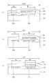
도 4는 본 발명에 따른 액정표시장치의 박막트랜지스터 어레이기판에 형성된 트랜지스터부와 캐패시터부를 나타낸 평면도로서, 픽셀지역에 형성된 게이트라인과 캐패시터부의 배치구조를 나타낸 평면도로서, (a)는 A영역(전체 화소영역의 상측 가장자리지역), (b)는 B영역(전체 화소영역의 중앙지역), (c)는 C영역(전체 화소영역의 하측 가장자리지역)을 도시한 평면도.FIG. 4 is a plan view showing a transistor portion and a capacitor portion formed in a thin film transistor array substrate of a liquid crystal display according to the present invention. FIG. 4 is a plan view showing an arrangement structure of a gate line and a capacitor portion formed in a pixel region. (B) is a plan view showing region B (center region of the entire pixel region), and (c) region C (bottom edge region of the entire pixel region).
도 5는 본 발명에 따른 액정표시장치의 게이트라인과 캐패시터부의 배치구조를 개략적으로 도시한 단면도로서, (a)는 도 4(a)의 Ⅴa-Ⅴa 선에 따른 단면도이 고, (b)는 도 4(b)의 Ⅴb-Ⅴb 선에 따른 단면도이며, (c)는 도 4(c)의 Ⅴc-Ⅴc 선에 따른 단면도.FIG. 5 is a cross-sectional view schematically illustrating an arrangement structure of a gate line and a capacitor unit of a liquid crystal display according to the present invention, (a) is a cross-sectional view taken along the line Va-Va of FIG. 4 (a), and (b) 4 (b) is a cross-sectional view taken along the line Vb-Vb, and (c) is a cross-sectional view taken along the line Vc-Vc in FIG. 4 (c).
- 도면의 주요부분에 대한 부호설명 -DESCRIPTION OF THE PREFERRED EMBODIMENTS -
101 : 어레이기판103a : 제1 게이트라인101:
103b : 제2 게이트라인103c : 제3 게이트라인103b:
105a : 제1 하부전극105b : 제2 하부전극105a: first
105c : 제3 하부전극107 : 게이트절연막105c: third lower electrode 107: gate insulating film
109 : 데이터라인 111 : 소스전극109
113a : 제1 상부전극113b : 제2 상부전극113c : 제3 상부전극115 : 보호막113a: first
A : 제1 블럭B : 제2 블럭A: first block B: second block
C : 제3 블럭Wg1 : 제1 게이트라인 폭C: third block Wg1: first gate line width
Wg2 : 제2 게이트라인 폭 Wg3 : 제3 게이트라인 폭Wg2: second gate line width Wg3: third gate line width
Wc1 : 제1 하부전극 폭Wc2 : 제2 하부전극 폭 Wc3 : 제3 하부전극 폭Wc1: first lower electrode width Wc2: second lower electrode width Wc3: third lower electrode width
본 발명은 액정표시장치에 관한 것으로서, 보다 상세하게는 액정표시패널의 단위 화소의 위치별로 발생하는 플리커(flicker) 편차를 보상하고자 한 액정표시장 치 및 그 제조방법에 관한 것이다.BACKGROUND OF THE INVENTION 1. Field of the Invention The present invention relates to a liquid crystal display device, and more particularly, to a liquid crystal display device and a method of manufacturing the same, to compensate for a flicker variation occurring for each position of unit pixels of a liquid crystal display panel.
일반적으로, 화상정보를 화면에 나타내는 화면표시장치들중에서 브라운관 표시장치(CRT; cathode ray tube)가 지금까지 가장 많이 사용되어 왔는데, 이것은 표시 면적에 비해 부피가 크고 무겁기 때문에 사용하는데 많은 불편함이 있었다.In general, cathode ray tube (CRT) has been the most used among the display devices for displaying image information on the screen, which is inconvenient to use because it is bulky and heavy compared to the display area. .
이에 따라, 표시면적이 크더라도 그 두께가 얇아서 어느 장소에서든지 쉽게 사용할 수 있는 박막형 평판표시장치가 개발되어지면서 점점 브라운관 표시장치를 대체하고 있다.Accordingly, even when the display area is large, a thin film type flat panel display device having a small thickness and being easily used in any place has been developed, and is gradually replacing the CRT display device.
특히, 액정표시장치(LCD; liquid crystal display device)는 표시 해상도가 다른 평판표시장치보다 뛰어나고, 동화상을 구현할때 그 품질이 브라운관에 비할 만큼 반응속도가 빠른 특성을 가지고 있다.In particular, a liquid crystal display (LCD) has a characteristic that the display resolution is superior to other flat panel display devices, and that the quality of the response is faster than that of a CRT when a moving image is realized.
이러한 액정표시장치는 기본적으로 적어도 한쪽이 투명한 유리 등으로 이루어지는 두 장의 기판사이에 액정층을 협지한 소위 액정패널로 구성한다.Such a liquid crystal display device is basically composed of a so-called liquid crystal panel in which at least one of the liquid crystal layers is sandwiched between two substrates made of transparent glass or the like.
이는 일반적으로 그 구조 및 구동방법에 따라 크게 수동 매트릭스(passive matrix)형 및 액티브 매트릭스(active matrix)형 액정표시장치로 나누어진다.It is generally divided into a passive matrix type and an active matrix type liquid crystal display device according to its structure and driving method.
수동 매트릭스형 액정표시장치는 액티브 매트릭스형에 비해 제작이 용이하고 구동방법이 간단하다는 장점을 갖고 있으나, 전력소모가 크고 주사선(scan line)의 수가 늘어날수록 구동이 어려워진다는 단점이 있다.The passive matrix type liquid crystal display device has advantages in that it is easier to manufacture and simpler in driving method than the active matrix type. However, the passive matrix type liquid crystal display device has a disadvantage in that driving becomes more difficult as power consumption increases and the number of scan lines increases.
이에 반해, 능동 매트릭스형 액정표시장치는 수동매트릭스형의 구성과는 달리 다수의 화소영역마다 박막트랜지스터가 포함되어, 상기 다수의 화소영역내부의 각 화소부를 독립적으로 구동할 수 있도록 하므로 정교한 소자를 만드는 경우에 효 율적이라는 장점이 있다.On the contrary, unlike the passive matrix type, the active matrix liquid crystal display device includes a thin film transistor in each pixel area, and thus, each pixel part in the plurality of pixel areas can be driven independently, thereby making a sophisticated device. In this case, there is an advantage of being efficient.
이러한 액티브 매트릭스형 액정표시장치는 스위칭소자로서 박막트랜지스터를 이용하여 자연스러운 동화상을 표현하고 있다.Such an active matrix liquid crystal display uses a thin film transistor as a switching element to express a natural moving image.
이러한 일반적인 액정표시장치의 구성에 대해 도 1을 참조하여 개략적으로 설명하면 다음과 같다.A configuration of such a general liquid crystal display device will be described below with reference to FIG. 1.
도 1은 일반적인 액정표시장치를 개략적으로 설명하기 위한 평면도로서, 픽셀내의 픽셀지역에 따라 픽셀전압의 변동량 차이를 설명하기 위한 평면도이다.FIG. 1 is a plan view schematically illustrating a general liquid crystal display device, and is a plan view illustrating a difference in variation of pixel voltages according to pixel regions within a pixel.
도 1을 참조하면, 일반적인 액티브 매트릭스형 액정표시장치는 어레이기판 (11)상에 서로 교차되게 배열되어 있는 복수개의 게이트라인(미도시)과 복수개의 데이터라인(미도시)과, 이들 복수개의 게이트라인(미도시)과 복수개의 데이터라인(미도시)이 각각 연결된 게이트구동회로부(21)와 데이터구동회로부(31)와, 상기 복수개의 복수개의 게이트라인(미도시)과 복수개의 데이터라인(미도시)이 교차되는 지역에 형성되고 각 단위화소당 하나씩 구비된 박막트랜지스터(미도시)와, 상기 복수개의 게이트라인과 복수개의 데이터라인이 교차되어 이루는 영역에 정의된 화소영역(41)과, 블랙매트릭스(미도시)와 칼라필터층(미도시)이 형성된 칼라필터기판(미도시) 및, 상기 칼라필터기판과 어레이기판(11)사이에 충진된 액정층(미도시)을 포함하여 구성된다.Referring to FIG. 1, a general active matrix liquid crystal display device includes a plurality of gate lines (not shown) and a plurality of data lines (not shown) arranged on the
여기서, 도면에는 도시하지 않았지만, 상기 게이트라인은 상기 박막트랜지스터의 게이트전극을 구동하는 펄스전압을 전달하며, 상기 데이터라인은 상기 박막트랜지스터의 소스전극을 구동하는 신호전압을 전달하는 수단이다.Although not shown in the drawing, the gate line transfers a pulse voltage driving the gate electrode of the thin film transistor, and the data line transfers a signal voltage driving the source electrode of the thin film transistor.
이때, 상기 게이트전극의 신호에 의해 임의의 소스전극에 액정을 구동할 수 있는 전압이 인가되고, 나머지에는 액정 구동전압보다 작은 전압이 인가된다면 액정구동전압이 인가된 화소만 동작한다.In this case, when a voltage capable of driving the liquid crystal is applied to an arbitrary source electrode by the signal of the gate electrode, and a voltage smaller than the liquid crystal driving voltage is applied to the rest, only the pixel to which the liquid crystal driving voltage is applied operates.
즉, 상기 액티브 매트릭스형 액정표시장치는 스위칭소자로서의 박막트랜지스터와 상, 하판 전극 즉, 공통전극 및 화소전극사이의 액정의 존재로 인해 형성되는 캐패시터, 보조 캐패시터, 게이트라인 및 데이터라인을 구비한다.That is, the active matrix liquid crystal display includes a thin film transistor as a switching element, and a capacitor, an auxiliary capacitor, a gate line, and a data line formed due to the presence of liquid crystal between upper and lower electrodes, that is, the common electrode and the pixel electrode.
또한, 상기 액정표시장치를 구동하는 경우, 먼저 게이트전극에 일정한 전압이 인가되면 박막트랜지스터가 턴온(turn on)되고, 이 시간동안에 화상에 관한 정보를 가진 데이터신호가 상기 박막트랜지스터를 통해 액정(미도시)에 인가된다.In the case of driving the liquid crystal display, first, when a constant voltage is applied to the gate electrode, the thin film transistor is turned on, and during this time, a data signal having information about an image is transferred to the liquid crystal (not shown) through the thin film transistor. Is applied).
이때, 캐패시터인 액정부분은 충전되는데, 이상적인 경우 액정에 충전된 총전하량은 게이트가 턴오프(turn off)되어 다음 신호가 들어올 때까지 유지된다.At this time, the liquid crystal portion, which is a capacitor, is charged. In an ideal case, the total charge charged in the liquid crystal is maintained until the gate is turned off and the next signal is input.
픽셀전압(Vp)은 액정표시장치에서 발생되는 다수의 캐패시턴스의 존재로 인하여 ΔVp 만큼의 변동이 있으며, ΔVp 는 근사적으로 다음의 식(1)에 의해 표현된다.The pixel voltage Vp varies by ΔVp due to the presence of a plurality of capacitances generated in the liquid crystal display, and ΔVp is approximately expressed by the following equation (1).
ΔVp = Cgs × ΔVg / Cgs + Clc + Cst ---------------- (1)ΔVp = Cgs × ΔVg / Cgs + Clc + Cst ---------------- (1)
여기서, ΔVp는 픽셀전압의 변동량이고, Cgs는 게이트전극과 소스전극의 중첩으로 존재하는 기생축적용량이며, Clc는 화소용량이며, Cst는 스토리지 캐패시터의 축적용량이며, ΔVg는 게이트전압의 하이(high level)전압과 로우(low level)전압 차이를 나타낸다.Here, ΔVp is a variation of pixel voltage, Cgs is a parasitic storage capacitance that overlaps with a gate electrode and a source electrode, Clc is a pixel capacitance, Cst is a storage capacitor storage capacitor, and ΔVg is a high voltage of gate voltage. The difference between level voltage and low level voltage is shown.
이와 같이, ΔVp 즉, 픽셀전압의 변동량은 액정전압의 왜곡을 발생시키기 때 문에 플리커(flicker)의 주요 원인이 된다.As described above, ΔVp, that is, the amount of change in the pixel voltage causes distortion of the liquid crystal voltage, which is a major cause of flicker.
도 2를 참조하면, 상기 픽셀전압의 변동량(ΔVp)은 액정표시패널의 전체 화소영역중 상부 가장자리쪽 즉, 제1 내지 제 m 번째 게이트라인과 제1 내지 제 n 번째 데이터라인중 제1게이트라인과 제1 데이터라인쪽에 위치하는 화소영역으로 갈수록 증가한다.Referring to FIG. 2, the variation amount ΔVp of the pixel voltage is the upper edge side of all pixel regions of the liquid crystal display panel, that is, the first gate line of the first to mth gate lines and the first to nth data lines. And increase toward the pixel area positioned toward the first data line.
즉, 전체 화소영역을 복수개의 블럭으로 구분할때, 제1게이트라인 및 제1데이터라인쪽으로 갈수록 픽셀전압의 변동량(ΔVp)은 증가한다.That is, when the entire pixel area is divided into a plurality of blocks, the variation amount ΔVp of the pixel voltage increases toward the first gate line and the first data line.
예를들어, 제1게이트라인을 기준으로, 제1 내지 제 n번째 데이터라인을 비교해 볼때 제1데이터라인쪽으로 갈수록 픽셀전압의 변동량(ΔVp)은 증가한다.For example, when comparing the first to nth data lines with respect to the first gate line, the variation amount ΔVp of the pixel voltage increases toward the first data line.
그리고, 제1데이터라인을 기준으로, 제1 내지 제 m 번째 게이트라인을 비교해 볼때 제1 게이트라인쪽으로 갈수록 픽셀전압의 변동량(ΔVp)은 증가한다.When the first to m th gate lines are compared with respect to the first data line, the variation amount ΔVp of the pixel voltage increases toward the first gate line.
또한, 도면에는 도시하지 않았지만, 종래기술에 따른 액정표시장치의 각 단위화소를 구성하는 캐패시터 구조는 전체 화소에 대해 동일한 크기로 형성되어 있다. 즉, 캐패시터를 구성하는 캐패시터 하부전극과 상부전극 및 이들사이에 형성되는 게이트절연막의 크기를 동일하게 형성하므로써, 동일한 축적용량(캐패시턴스)을갖도록 구성되어 있다.Although not shown in the drawings, the capacitor structure constituting each unit pixel of the liquid crystal display according to the related art is formed in the same size for all the pixels. In other words, the capacitors have the same storage capacitance (capacitance) by forming the same size of the capacitor lower electrode, the upper electrode, and the gate insulating film formed therebetween.
한편, 액정표시패널의 크기가 증가함에 따라 필수적으로 많은 수의 게이트버스라인과 데이터버스라인을 갖게 되고, 그에 따라 전체 축적용량은 증가하게 된다. On the other hand, as the size of the liquid crystal display panel increases, there is essentially a large number of gate bus lines and data bus lines, thereby increasing the total storage capacity.
상기한 바와같이, 종래기술에 따른 액정표시장치에 의하면 다음과 같은 문제 점이 있다.As described above, the liquid crystal display according to the related art has the following problems.
종래기술에 따른 액정표시장치는, 이러한 캐패시턴스의 증가로 인해 RC 딜레이(delay)에 의한 구동신호의 왜곡(distortion)을 발생시킨다.In the liquid crystal display according to the related art, such an increase in capacitance causes distortion of a driving signal due to an RC delay.
이와 같이 RC 딜레이에 의해 발생되는 구동신호의 왜곡은 기판상의 좌우에 대하여 픽셀전압의 변동량(ΔVp) 차이를 발생시켜 플리커(flicker)를 야기시킨다.As described above, the distortion of the driving signal generated by the RC delay causes a difference in the amount of change of the pixel voltage (ΔVp) with respect to the left and right on the substrate, causing flicker.
따라서, 배선 딜레이(line delay)가 커짐에 따라 TFT의 차징(charging)이 어려워진다.Therefore, charging of the TFT becomes difficult as the line delay increases.
한편, LCD TV가 보편화됨에 따라 고해상도 패널의 요구가 증가하고 있는데, 고해상도의 패널의 경우, 배선의 기생 캐패시턴스가 더욱 증가하기 때문에 차징 (charging) 문제가 더욱 심각해진다.On the other hand, as LCD TVs are becoming more common, the demand for high resolution panels is increasing. In the case of high resolution panels, the charging problem becomes more serious because parasitic capacitance of wiring is further increased.
또한, 게이트라인의 딜레이(delay)가 증가함에 따라 액정표시패널의 좌우 상하 델타 Vp(즉, ΔVp)가 달라지므로써 액정표시패널이 전체적으로 불균일하게 떨리는 화질 불량이 발생하게 된다.Also, as the delay of the gate line increases, the left and right upper and lower delta Vp (that is, ΔVp) of the liquid crystal display panel is changed, resulting in an image quality defect in which the liquid crystal display panel shakes unevenly as a whole.
이러한 플리커(flicker)를 조정하기 위하여 공통전압을 조정하지만 게이트라인 딜레이(gate line delay)가 큰 경우, 액정표시패널내의 플리커(flicker)의 전체적인 균일도가 떨어지며, 상하 좌우 비대칭적으로 떨림이 발생하므로 Vcom 조정이 어렵다.In order to control the flicker, if the common voltage is adjusted, but the gate line delay is large, the overall uniformity of the flicker in the liquid crystal display panel decreases, and asymmetrical shaking occurs in the vertical, horizontal, and horizontal directions. Difficult to adjust
한편, 게이트라인의 저항을 보상하기 위하여 선폭 및 두께를 조정하는 방법에는 한계가 존재한다.On the other hand, there is a limit to the method of adjusting the line width and thickness to compensate for the resistance of the gate line.
즉, 저항을 낮추기 위하여 게이트라인의 선폭을 늘릴 경우에 픽셀의 개구율 이 감소하게 되어, 전반적인 패널의 휘도가 감소하게 된다.In other words, when the line width of the gate line is increased in order to lower the resistance, the aperture ratio of the pixel is decreased, thereby reducing the overall luminance of the panel.
그에 따라 휘도를 맞추기 위하여 고효율 시트(sheet) 등을 사용해야 하므로 비용이 증가하는 문제점이 있다.Accordingly, there is a problem in that the cost is increased because a high efficiency sheet or the like must be used to adjust the luminance.
또한, 증착 두께를 증가시켜 저항을 낮출 경우에, 식각후 테이퍼(taper) 등이 나빠져서 공정상의 불량을 유발할 수 있는 확률이 커진다.In addition, in the case of lowering the resistance by increasing the deposition thickness, the taper or the like worsens after etching, thereby increasing the probability of causing a process defect.
따라서, 배선 형성후 절연막 증착시에 보이드(void) 형성 등에 의하여 배선간 쇼트 (short) 등이 발생한다.Therefore, a short between wirings occurs due to void formation or the like during the deposition of the insulating film after wiring formation.
이에 본 발명은 상기 종래기술의 제반 문제점을 해결하기 위하여 안출한 것으로서, 본 발명의 목적은 액정표시패널내의 단위화소의 위치별로 발생하는 플리커 (flicker) 편차를 보상할 수 있는 액정표시장치 및 그 제조방법을 제공함에 있다.Accordingly, the present invention has been made to solve the above-mentioned problems of the prior art, and an object of the present invention is to provide a liquid crystal display device capable of compensating for the flicker variation occurring for each position of unit pixels in the liquid crystal display panel, and a manufacture thereof. In providing a method.
상기 목적을 달성하기 위한 본 발명에 따른 액정표시장치는, 어레이기판에 형성되고, 서로 다른 크기를 가진 제1 내지 제 m 번째 게이트라인; 상기 어레이기판에 형성되고 서로 다른 크기를 가진 제1 내지 제 m 번째 게이트라인과 이격된 서로 다른 크기를 가진 제1 내지 제 m 번째 캐패시터 하부전극; 상기 어레이기판상에 형성되고 상기 제1 내지 제 m 번째 게이트라인과 교차되어 배열되는 제1 내지 제 n 번째 데이터라인; 상기 제1 내지 제 m 번째 게이트라인과 상기 제1 내지 제 n 번째 데이터라인이 교차되어 이루는 영역에 정의되는 복수개의 픽셀영역; 상기 어레이기판상에 형성되고, 상기 제1 내지 제 m 번째 게이트라인과 상기 제1 내지 제 n 번째 데이터라인이 서로 교차되는 부분에 형성된 복수개의 박막트랜지스터부; 및 상기 어레이기판상에 형성되고, 상기 박막트랜지스터부와 연결되어 상기 서로 다른 크기를 가진 제1 내지 제 m 번째 캐패시터 하부전극과 대응하여 서로 다른 크기를 가진 캐패시터를 구성하는 제1 내지 제 m 번째 캐패시터 상부전극;을 포함하여 구성되는 것을 특징으로한다.According to an aspect of the present invention, there is provided a liquid crystal display device comprising: first to mth gate lines formed on an array substrate and having different sizes; First to m-th capacitor lower electrodes formed on the array substrate and spaced apart from the first to m-th gate lines having different sizes; First to nth data lines formed on the array substrate and arranged to cross the first to mth gate lines; A plurality of pixel regions defined in regions where the first to m th gate lines intersect the first to n th data lines; A plurality of thin film transistors formed on the array substrate and formed at portions where the first to m th gate lines and the first to n th data lines cross each other; And first to mth capacitors formed on the array substrate and connected to the thin film transistors to form capacitors having different sizes to correspond to the first to mth capacitor lower electrodes having different sizes. An upper electrode; characterized in that comprises a.
상기 목적을 달성하기 위한 본 발명에 따른 액정표시장치는, 어레이기판에 형성되고, 서로 다른 폭을 가진 제1 내지 제 m 번째 게이트라인; 상기 어레이기판에 형성되고 서로 다른 폭을 가진 제1 내지 제 m 번째 게이트라인과 이격된 서로 다른 폭을 가진 제1 내지 제 m 번째 캐패시터 하부전극; 상기 어레이기판상에 형성되고 상기 제1 내지 제 m 번째 게이트라인과 교차되어 배열되는 제1 내지 제 n 번째 데이터라인; 상기 제1 내지 제 m 번째 게이트라인과 상기 제1 내지 제 n 번째 데이터라인이 교차되어 이루는 영역에 정의되는 복수개의 픽셀영역; 상기 어레이기판상에 형성되고, 상기 제1 내지 제 m 번째 게이트라인과 상기 제1 내지 제 n 번째데이터라인이 서로 교차되는 부분에 형성된 복수개의 박막트랜지스터부; 상기 어레이기판상에 형성되고, 상기 박막트랜지스터부와 연결되어 상기 서로 다른 폭을 가진 제1 내지 제 m 번째 캐패시터 하부전극과 대응하여 서로 다른 폭을 가진 캐패시터를 구성하는 제1 내지 제 m 번째 캐패시터 상부전극; 상기 어레이기판상에 형성되고, 상기 박막트랜지스터와 전기적으로 접속되는 화소전극; 상기 어레이기판과 합착되고, 블랙매트릭스와 칼라필터층이 구비된 칼라필터기판; 및 상기 어레이기판과 칼라필터기판사이에 형성된 액정층;을 포함하여 구성되는 것을 특징으로한다.According to an aspect of the present invention, there is provided a liquid crystal display device comprising: first to m-th gate lines formed on an array substrate and having different widths; First to m-th capacitor lower electrodes formed on the array substrate and having different widths spaced apart from the first to m-th gate lines having different widths; First to nth data lines formed on the array substrate and arranged to cross the first to mth gate lines; A plurality of pixel regions defined in regions where the first to m th gate lines intersect the first to n th data lines; A plurality of thin film transistors formed on the array substrate and formed at portions where the first to m th gate lines and the first to n th data lines cross each other; First to m-th capacitors formed on the array substrate and connected to the thin film transistors to form capacitors having different widths corresponding to the first to m-th capacitor lower electrodes having different widths. electrode; A pixel electrode formed on the array substrate and electrically connected to the thin film transistor; A color filter substrate bonded to the array substrate and provided with a black matrix and a color filter layer; And a liquid crystal layer formed between the array substrate and the color filter substrate.
상기 목적을 달성하기 위한 본 발명에 따른 액정표시장치 제조방법은, 어레이기판에 서로 다른 크기를 가진 제1 내지 제 m 번째 게이트라인과 캐패시터 하부전극을 형성하는 단계; 상기 서로 다른 크기를 가진 제1 내지 제 m 번째 게이트라인과 캐패시터 하부전극을 포함한 어레이기판상에 게이트절연막을 형성하는 단계; 상기 게이트절연막상에 액티브층을 형성하는 단계; 상기 액티브층상에 상기 제1 내지 제 m 번째 게이트라인과 교차되게 배열되어 복수개의 화소영역을 정의하는 제1 내지 제 n 번째 데이터라인과 서로 이격된 소스/드레인전극을 형성하는 단계; 상기 어레이기판 전체에 보호막을 형성하는 단계; 상기 보호막을 선택적으로 패터닝하여 상기 제1 내지 제m 번째 드레인전극을 노출시키는 콘택홀을 형성하는 단계; 및 상기 보호막상에 상기 콘택홀을 통해 상기 제1 내지 제m 번째 드레인전극과 전기적으로 접속되는 화소전극을 형성하는 단계를 포함하여 구성되는 특징으로한다.According to an aspect of the present invention, there is provided a method of manufacturing a liquid crystal display device, the method comprising: forming first to m-th gate lines and a capacitor lower electrode having different sizes on an array substrate; Forming a gate insulating film on the array substrate including the first to mth gate lines having a different size and a capacitor lower electrode; Forming an active layer on the gate insulating film; Forming a source / drain electrode on the active layer to be spaced apart from the first to nth data lines arranged to cross the first to mth gate lines to define a plurality of pixel areas; Forming a protective film on the entire array substrate; Selectively patterning the passivation layer to form a contact hole exposing the first to mth drain electrodes; And forming a pixel electrode on the passivation layer, wherein the pixel electrode is electrically connected to the first to mth drain electrodes through the contact hole.
상기 목적을 달성하기 위한 본 발명에 따른 액정표시장치 제조방법은, 어레이기판에 서로 다른 폭을 가진 제1 내지 제 m 번째 게이트라인과 캐패시터 하부전극 및 게이트전극을 형성하는 단계; 상기 서로 다른 폭을 가진 제1 내지 제 m 번째 게이트라인과 캐패시터 하부전극을 포함한 어레이기판상에 게이트절연막을 형성하는 단계; 상기 게이트절연막상에 액티브층을 형성하는 단계; 상기 액티브층상에 상기 제1 내지 제 m 번째 게이트라인과 교차되게 배열되어 복수개의 화소영역을 정의하는 제1 내지 제 n 번째 데이터라인과 서로 이격된 소스/드레인전극을 형성하는 단계; 상기 어레이기판 전체에 보호막을 형성하는 단계; 상기 보호막을 선택적으로 패터닝하여 상기 제1 내지 제m 번째 드레인전극을 노출시키는 콘택홀을 형성하는 단계; 상기 보호막상에 상기 콘택홀을 통해 상기 제1 내지 제m 번째 드레인전극과 전기적으로 접속되는 화소전극을 형성하는 단계; 상기 어레이기판과 합착되는 컬라필터기판상에 블랙매트릭스와 칼라필터층을 형성하는 단계; 및 상기 어레이기판과 칼라필터기판사이에 액정층을 형성하는 단계;를 포함하여 구성되는 특징으로한다.According to an aspect of the present invention, there is provided a method of manufacturing a liquid crystal display device, the method comprising: forming first to m-th gate lines, a capacitor lower electrode, and a gate electrode having different widths on an array substrate; Forming a gate insulating film on the array substrate including the first to mth gate lines having a different width and a capacitor lower electrode; Forming an active layer on the gate insulating film; Forming a source / drain electrode on the active layer to be spaced apart from the first to nth data lines arranged to cross the first to mth gate lines to define a plurality of pixel areas; Forming a protective film on the entire array substrate; Selectively patterning the passivation layer to form a contact hole exposing the first to mth drain electrodes; Forming a pixel electrode on the passivation layer, the pixel electrode being electrically connected to the first to mth drain electrodes through the contact hole; Forming a black matrix and a color filter layer on the color filter substrate bonded to the array substrate; And forming a liquid crystal layer between the array substrate and the color filter substrate.
이하, 본 발명에 따른 액정표시장치 및 그 제조방법에 대해 첨부된 도면을 참조하여 상세히 설명한다.Hereinafter, a liquid crystal display and a manufacturing method thereof according to the present invention will be described in detail with reference to the accompanying drawings.
도 3은 본 발명에 따른 액정표시장치를 개략적으로 설명하기 위한 평면도로서, 패널내의 픽셀지역과 함께 이 픽셀지역에 따라 픽셀전압의 변동량 차이를 설명하기 위한 평면도이다.3 is a plan view schematically illustrating a liquid crystal display device according to an exemplary embodiment of the present invention, and a plan view for explaining a difference in pixel voltage variation according to the pixel region together with the pixel region in the panel.
도3을 참조하면, 본 발명에 따른 액정표시장치는, 어레이기판(101)의 일측 단변 및 일측 장변이 돌출되도록 상기 어레이기판(101)과 칼라필터기판(미도시)이 합착되며, 그 어레이기판(101)과 칼라필터기판(미도시)의 합착된 영역내에 복수의 화소들이 매트릭스 형태로 배열되는 화상표시부(141)가 마련되어 있다.Referring to FIG. 3, in the liquid crystal display according to the present invention, the
또한, 상기 화상 표시부(141)의 어레이기판(101)에는 일정하게 이격되어 종으로 배열되는 복수의 게이트 라인(미도시)들과, 일정하게 이격되어 횡으로 배열되는 복수의 데이터 라인(미도시)들 및, 그 게이트 라인들과 데이터 라인들의 교차영역마다 픽셀들이 정의되어 매트릭스 형태로 배열된다.In addition, the
그리고, 상기 복수의 화소들 각각에는 스위칭소자로 박막 트랜지스터와 함께 이 박막트랜지스터에 전기적으로 접속되는 화소전극이 형성된다.Each pixel includes a thin film transistor as a switching element and a pixel electrode electrically connected to the thin film transistor.
여기서, 도면에 도시하지 않았지만, 상기 박막 트랜지스터는 상기 게이트 라 인들과 동시에 패터닝되어 게이트 라인들과 전기적으로 접속되는 게이트 전극과, 상기 데이터 라인들과 동시에 패터닝되어 데이터 라인들과 전기적으로 접속되는 소스전극과, 상기 데이터 라인들 및 소스전극과 동시에 패터닝되어 상기 화소전극과 전기적으로 접속되는 드레인전극으로 구성된다.Although not shown in the drawings, the thin film transistor may include a gate electrode patterned at the same time as the gate lines and electrically connected to gate lines, and a source patterned at the same time as the data lines and electrically connected to the data lines. And a drain electrode patterned simultaneously with the data lines and the source electrode and electrically connected to the pixel electrode.
또한, 도면에는 도시하지 않았지만, 상기 화상표시부(141)의 칼라필터기판 (미도시)에는 광투과를 차단하는 블랙 매트릭스(미도시)와 이 블랙매트릭스에 의해 화소별로 분리되어 도포된 적, 녹, 청 색상의 칼러필터들이 형성되어 있다.Although not shown in the drawings, a color matrix (not shown) of the
그리고, 상기 어레이기판(101)과 칼라필터기판(미도시)은 화상표시부(141)의 외곽을 따라 형성되는 실패턴(미도시)에 의해 합착된다.In addition, the
이때, 상기 어레이기판(101)이나 칼라필터기판(미도시)상에는 무작위로 산포된 스페이서-볼(spacer ball)이나 포토리쏘그래피(photo-lithography) 공정을 통해 패턴화된 스페이서(patterned spacer)가 형성된다.At this time, a patterned spacer is formed on the
또한, 상기 어레이기판(101)과 칼라필터기판은 상기 스페이서-볼이나 스페이서에 의해 일정한 이격간격을 갖게 되며, 그 이격간격에 액정층(미도시)이 형성된다.In addition, the
한편, 상기 어레이기판(101)의 돌출된 일측 단변에는 상기 화상표시부(141)와 대응되는 영역에 상기 게이트 라인들과 전기적으로 접속되어 게이트 라인들에 구동신호들을 공급하는 게이트구동회로부(121)가 형성되어 있다.On the other hand, at one protruding short side of the
또한, 상기 어레이기판(101)의 돌출된 일측 장변에는 상기 화상표시부(141)와 대응되는 영역에 상기 데이터라인들과 전기적으로 접속되어 데이터라인들에 화 상정보를 공급하는 데이터구동회로부(131)가 형성되어 있다.In addition, a data driving
그리고, 상기 박막 트랜지스터 어레이기판(101)의 단변 일측 및 장변 일측이 만나는 모서리부분에는 제1 라인-온-글래스(LOG; line on glass)배선(133)이 구비되어져 상기 데이터구동회로부(131)로부터 제어신호 및 구동전압을 상기 게이트구동회로부(121)로 공급한다.In addition, a first line-on-glass (LOG)
상기 제1 라인-온-글래스배선(133)을 통해 게이트구동회로부(121)에 공급되는 구동전압들은 게이트 하이전압(Vgh), 게이트 로우전압(Vgl), 공통전압(Vcom), 접지전압(GND) 및 전원전압(Vcc) 등과 같은 직류 신호들이다.The driving voltages supplied to the gate driving
또한, 상기 제1 라인-온-글래스 배선(133)을 통해 게이트구동회로부(121)에 공급되는 제어신호들은 게이트 스타트 펄스(GSP), 게이트 쉬프트 클럭(GSC) 및 게이트 인에이블 신호(GOE) 등과 같은 교류 신호들이다.In addition, the control signals supplied to the gate driving
상기한 바와 같은 제1 라인-온-글래스 배선(133)들은 상기 박막 트랜지스터 어레이 기판(101)상에 게이트라인들 및 게이트 전극들을 형성하는 공정에서 동시에 패터닝되어 형성된다.The first line-on-
한편, 제2 라인-온-글래스배선(123)은 m 번째 게이트구동회로부(121)와 또다른 m-1번째 게이트구동회로부(121)을 연결하도록 구성되어 있다.On the other hand, the second line-on-
또한, 상기 어레이기판(101)에는 상기 게이트라인(도 4의 103a, 103b, 103c)과 일정간격을 두고 캐패시터 하부전극(도 4의 105a, 105b, 105c)이 형성되어 있고 이 캐패시터 하부전극상에는 게이트절연막(도 4의 107)을 사이에 두고 캐패시터 상부전극(도 4의 113a, 113b, 113c)이 형성되어져 캐패시터를 구성한다. 이때, 상기 캐패시터 상부전극은 드레인전극으로도 사용되며, 화소전극(도 4의 117)과 전기적으로 접속된다.In addition, a capacitor lower electrode (105a, 105b, 105c of FIG. 4) is formed on the
상기에서와 같이, 본 발명에 따른 액정표시장치는 스위칭소자로서의 박막트랜지스터와 공통전극 및 화소전극사이의 액정의 존재로 인해 형성되는 캐패시터, 보조 캐패시터, 게이트라인 및 데이터라인을 구비한다.As described above, the liquid crystal display according to the present invention includes a capacitor, an auxiliary capacitor, a gate line, and a data line formed due to the presence of the liquid crystal between the thin film transistor as the switching element and the common electrode and the pixel electrode.
또한, 상기 액정표시장치를 구동하는 경우, 먼저 게이트전극에 일정한 전압이 인가되면 박막트랜지스터가 턴온(turn on)되고, 이 시간동안에 화상에 관한 정보를 가진 데이터신호가 상기 박막트랜지스터를 통해 액정(미도시)에 인가된다.In the case of driving the liquid crystal display, first, when a constant voltage is applied to the gate electrode, the thin film transistor is turned on, and during this time, a data signal having information about an image is transferred to the liquid crystal (not shown) through the thin film transistor. Is applied).
이때, 캐패시터인 액정부분은 충전되는데, 이상적인 경우 액정에 충전된 총전하량은 게이트가 턴오프(turn off)되어 다음 신호가 들어올 때까지 유지된다.At this time, the liquid crystal portion, which is a capacitor, is charged. In an ideal case, the total charge charged in the liquid crystal is maintained until the gate is turned off and the next signal is input.
전술한 바와같이, 픽셀전압은 액정표시장치에서 발생되는 다수의 캐패시턴스의 존재로 인하여 ΔVp 만큼의 변동이 있으며, ΔVp 는 근사적으로 다음의 식(1)에 의해 표현된다.As described above, the pixel voltage varies by ΔVp due to the presence of a plurality of capacitances generated in the liquid crystal display, and ΔVp is approximately expressed by the following equation (1).
ΔVp = Cgs × ΔVg / Cgs + Clc + Cst ---------------- (1)ΔVp = Cgs × ΔVg / Cgs + Clc + Cst ---------------- (1)
여기서, ΔVp는 픽셀전압의 변동량이고, Cgs는 게이트전극과 소스전극의 중첩으로 존재하는 기생축적용량이며, Clc는 화소용량이며, Cst는 스토리지 캐패시터의 축적용량 및 ΔVg는 게이트전압의 하이(high level)전압과 로우(low level)전압간 차이를 나타낸다.Here, ΔVp is a variation of pixel voltage, Cgs is a parasitic storage capacitance existing as a superposition of the gate electrode and the source electrode, Clc is the pixel capacitance, Cst is the storage capacitor storage capacity and ΔVg is the high level of the gate voltage. The difference between the voltage and the low level voltage.
이와 같이, ΔVp 즉, 픽셀전압의 변동량은 픽셀전압의 왜곡을 발생시키기 때문에 플리커(flicker)의 주요 원인이 된다.As described above, ΔVp, that is, the variation amount of the pixel voltage causes distortion of the pixel voltage, which is the main cause of flicker.
도 3 및 도 4를 참조하면, 상기 픽셀전압의 변동량(ΔVp)은 액정표시패널의 전체 화소영역중 상부 가장자리쪽 즉, 제1 내지 제 m 번째 게이트라인과 제1 내지 제 n 번째 데이터라인중 제1게이트라인과 제1 데이터라인쪽에 위치하는 화소영역으로 갈수록 증가한다.Referring to FIGS. 3 and 4, the variation amount ΔVp of the pixel voltage is the upper edge of all pixel areas of the liquid crystal display panel, that is, the first to mth gate lines and the first to nth data lines. Incrementally increases toward pixel areas positioned toward one gate line and the first data line.
예를들어, 제1게이트라인(103a)을 기준으로, 제1 내지 제 n 번째 데이터라인을 비교해 볼때 제1 데이터라인(109)쪽으로 갈수록 픽셀전압의 변동량(ΔVp)은 증가한다.For example, when comparing the first to nth data lines with respect to the
그리고, 제1데이터라인(109)을 기준으로, 제1 내지 제 m 번째 게이트라인 (103a, 103b, 103c)을 비교해 볼때 제1 게이트라인쪽으로 갈수록 픽셀전압의 변동량(ΔVp)은 증가한다. 즉, 횡방향의 제1 내지 제 n 번째 픽셀영역을 비교해 볼때, 제1번째 픽셀영역으로 갈수록 픽셀전압의 변동량(ΔVp)은 증가한다.When the first to m
또한, 종방향의 제1 내지 제 m 번째 픽셀영역을 비교해 볼때, 제1번째 픽셀영역으로 갈수록 픽셀전압의 변동량(ΔVp)은 증가한다.In addition, when comparing the first to m th pixel regions in the longitudinal direction, the variation amount ΔVp of the pixel voltage increases toward the first pixel region.
따라서, 본 발명에서는 전체 패널내의 화소위치별로 차이가 나는 픽셀전압의 변동량(ΔVp)을 거의 동일한 수준으로 보상해 주기 위해 각 단위 픽셀마다 캐패시터 크기를 달리 구성한다.Therefore, in the present invention, the capacitor size is configured differently for each unit pixel in order to compensate the amount of change (ΔVp) of the pixel voltage, which is different for each pixel position in the entire panel, to approximately the same level.
즉, 전체 화소영역내의 화소위치별로 차이가 나는 픽셀전압의 변동량(ΔVp)에 비례하도록 캐패시터의 크기를 달리 형성한다. 즉, 픽셀전압의 변동량(ΔVp)이 큰 지역의 캐패시터는 크게 형성하고, 픽셀전압의 변동량(ΔVp)이 작은 영역의 캐패시터는 작게 형성한다.That is, the size of the capacitor is formed differently so as to be proportional to the variation amount ΔVp of the pixel voltage which varies for each pixel position in the entire pixel region. In other words, the capacitor in the region where the variation amount ΔVp of the pixel voltage is large is formed large, and the capacitor in the region where the variation amount ΔVp of the pixel voltage is small is formed small.
상기 캐패시터의 축적용량(C)은 아래의 식(2)와 같이 나타낸다.The storage capacitance C of the capacitor is expressed by the following equation (2).
C = εA/d ----------------- (2) C = εA / d ----------------- (2)
여기서, C 는 축적용량, ε는 유전상수, A는 전극의 면적을 나타내며, d는 전극간의 거리를 나타낸다.Where C is the storage capacitance, ε is the dielectric constant, A is the area of the electrode, and d is the distance between the electrodes.
따라서, 본 발명에서는 캐패시터의 축적용량을 다르게 형성하기 위하여 A (전극의 면적) 즉, 캐패시터의 하부전극과 상부전극의 크기를 달리 형성한다.Therefore, in the present invention, in order to form a different capacitance of the capacitor, A (the area of the electrode), that is, different sizes of the lower electrode and the upper electrode of the capacitor are formed.
상기와 같이 각 지역에 따라 서로 다른 크기를 갖는 캐패시터를 구비한 액정표시장치를 제조하는 방법에 대해 도 4 및 도 5를 참조하여 설명하면 다음과 같다.A method of manufacturing a liquid crystal display device having a capacitor having a different size according to each region as described above will be described with reference to FIGS. 4 and 5.
도 4는 본 발명에 따른 액정표시장치의 박막트랜지스터 어레이기판에 형성된 트렌지스터부와 캐패시터부를 나타낸 평면도로서, 패널내의 픽셀지역에 형성된 게이트라인과 캐패시터부의 배치구조를 나타낸 평면도로서, (a)는 제1블럭(A영역)(전체 화소영역의 상측 가장자리지부), (b)는 제2블럭(B영역)(전체 화소영역의 중앙부), (c)는 제3블럭(C영역)(전체 화소영역의 하측 가장자리부)을 도시한 평면도이다.FIG. 4 is a plan view showing a transistor portion and a capacitor portion formed on a thin film transistor array substrate of the liquid crystal display according to the present invention, and (a) is a plan view showing an arrangement structure of a gate line and a capacitor portion formed in a pixel area of the panel. Block (area A) (upper edge portion of the entire pixel region), (b) is the second block (B region) (center portion of the entire pixel region), and (c) is the third block (C region) (all pixel regions It is a top view which shows the lower edge part.
도 5는 본 발명에 따른 액정표시장치의 게이트라인과 캐패시터의 배치구조를 개략적으로 도시한 단면도로서, (a)는 도 4(a)의 Ⅴa-Ⅴa 선에 따른 단면도이고, (b)는 도 4(b)의 Ⅴb-Ⅴb 선에 따른 단면도이며, (c)는 도 4(c)의 Ⅴc-Ⅴc 선에 따른 단면도이다.FIG. 5 is a cross-sectional view schematically illustrating an arrangement structure of a gate line and a capacitor of a liquid crystal display according to the present invention, (a) is a cross-sectional view taken along the line Va-Va of FIG. 4 (a), and (b) is a view It is sectional drawing along the Vb-Vb line of 4 (b), (c) is sectional drawing along the Vc-Vc line of FIG. 4 (c).
도 4 및 도 5를 참조하면, 제1블럭(A영역), 제2블럭(B영역), 제3 블럭(C영역)으로 분할된 어레이기판(101)상에 게이트전극(미도시)을 포함하는 제1, 2, 3 게이트라인 (103a) (103b) (103c)를 형성한다. 여기서, 본 발명에서는 패널의 전체 화소영역을 상기 제1, 2, 3 블럭(A영역, B영역, C영역)으로 분할한 경우를 가정하여 설명하기로 한다.4 and 5, a gate electrode (not shown) is included on the
이때, 상기 어레이기판(101)은 상기 제1, 2, 3 블럭(A영역, B영역, C영역)으로만 한정하는 것이 아니라 필요에 따라 3 블럭 이상으로도 분할하여 가정해 볼 수 있다.In this case, the
또는, 제1 내지 제 m 번째 게이트라인(103a) (103b) (103c) 각각을 기준으로, 제1 내지 제 n 번째 데이터라인(109)으로 구성되는 픽셀영역을 복수개의 블럭으로 분할하거나, 제1 내지 제 n 번째 데이터라인(109) 각각을 기준으로, 제1 내지 제 m번째 게이트라인(103a) (103b) (103c)으로 구성되는 픽셀영역을 복수개의 블럭으로 분할할 수도 있다.Alternatively, the pixel area composed of the first to
그리고, 제1데이터라인(109)을 기준으로, 제1 내지 제 m 번째 게이트라인 (103a) (103b) (103c)을 비교해 볼때 제1 게이트라인(103a)쪽의 픽셀영역으로 갈수록 픽셀전압의 변동량(ΔVp)은 증가한다. 즉, 횡방향의 제1 내지 제 n 번째 픽셀영역을 비교해 볼때, 제1번째 픽셀영역으로 갈수록 픽셀전압의 변동량(ΔVp)은 증가한다.When the first to m
또한, 종방향의 제1 내지 제 m 번째 픽셀영역을 비교해 볼때, 제1번째 픽셀영역으로 갈수록 픽셀전압의 변동량(ΔVp)은 증가한다.In addition, when comparing the first to m th pixel regions in the longitudinal direction, the variation amount ΔVp of the pixel voltage increases toward the first pixel region.
여기서는, 상기 제1블럭(A영역)은 화상표시부(141)의 상부 좌측 가장자리부를 나타내며, 상기 제2블럭(B영역)은 화상표시부(141)의 중앙부를 나타내며, 상기 제3블럭(C영역)은 화상표시부의 하부 우측 가장자리부를 나타낸다.Here, the first block (area A) represents the upper left edge of the
이때, 상기 제1게이트라인(103a)의 폭은 Wg1이고, 제2게이트라인(103b)의 폭은 Wg2이며, 제3게이트라인(103c)의 폭은 Wg3이다. 즉, 제1, 2, 3 게이트라인 (103a)(103b)(103c)의 폭 크기는 Wg1 〈 Wg2 〈 Wg3 순이다.In this case, the width of the
또한, 상기 제1, 2, 3 게이트라인(103a)(103b)(103c) 형성시에 이들 게이트라인과 일정간격을 두고 제1, 2, 3 캐패시터 하부전극(105a)(105b) (105c)도 함께 형성한다.In addition, the first, second and third capacitor
이때, 상기 제1캐패시터 하부전극(105a)의 폭은 Wc1이고, 제2캐패시터 하부전극(105b)의 폭은 Wc2이며, 제3캐패시터 하부전극(105c)의 폭은 Wc3이다. 즉, 제1, 2, 3 캐패시터 하부전극(105a)(105b)(105c)의 폭 크기는 Wc1 〉Wc2 〉Wc3 순이다.In this case, the width of the first capacitor
이어서, 상기 제1, 2, 3 게이트라인(103a)(103b)(103c)과 제1, 2, 3 캐패시터 하부전극(105a)(105b) (105c)을 포함한 어레이기판(101) 전체에 게이트절연막 (107)을 형성한다.Subsequently, a gate insulating film is formed on the
그다음, 상기 게이트절연막(107)상에 게이트전극(미도시)과 오버랩되도록 액티브층(미도시)을 형성한다.Next, an active layer (not shown) is formed on the
이때, 상기 액티브층(미도시)은 화상 표시부(도 3의 141)의 박막 트랜지스터가 형성되는 영역에서는 비정질 실리콘으로 이루어진 반도체층과, 인(P)이 고농도로 도핑된 n+ 비정질 실리콘으로 이루어진 오믹접촉층(미도시)이 연속 증착된 다음 패터닝되며, 후속공정에서 데이터라인 및 소스/드레인전극이 패터닝될 때, 노출된 오믹접촉층이 제거되어 박막 트랜지스터의 채널로 적용된다.At this time, the active layer (not shown) is an ohmic contact made of a semiconductor layer made of amorphous silicon and an n + amorphous silicon doped with phosphorus (P) in a region where the thin film transistor of the
따라서, 데이터라인 및 소스/드레인전극의 하부를 제외한 영역에서는 상기 오믹접촉층이 제거되어 반도체층만 잔류하게 된다.Accordingly, the ohmic contact layer is removed in regions except the lower portions of the data lines and the source / drain electrodes, so that only the semiconductor layer remains.
이어서, 상기 액티브층(미도시)을 포함한 어레이기판(101)상에 금속물질층을 형성한후 상기 금속물질층을 선택적으로 패터닝하여 데이터라인(109)과 함께 서로 일정간격만큼 이격된 소스전극(111) 및 제1, 2, 3 드레인전극(113a)(113b)(113c)을 형성한다.Subsequently, a metal material layer is formed on the
이때, 상기 제1, 2, 3, 드레인전극(113a)(113b)(113c)은 캐패시터의 상부전극으로도 사용된다.In this case, the first, second, third, and
또한, 상기 캐패시터의 상부전극으로 사용되는 제1, 2, 3, 드레인전극 (113a)(113b)(113c) 각각은 그 하부의 제1, 2, 3 캐패시터 하부전극 (113a) (113b) (113c)와 각각 오버랩되어져 제1, 2, 3 캐패시터를 형성한다.In addition, each of the first, second, and
그리고, 상기 제1, 2, 3, 드레인전극 (113a)(113b)(113c)의 폭 크기는 상기 제1, 2, 3 캐패시터 하부전극(105a)(105b)(105c)의 폭과 비례하도록 형성한다. 즉, 상기 제1, 2, 3, 드레인전극 (113a)(113b)(113c)의 폭은 제1 드레인전극(113a) 〉제2 드레인전극 (113b) 〉제3 드레인전극(113c) 순이다.The widths of the first, second, and
그다음, 상기 제1, 2, 3, 드레인전극 (113a)(113b)(113c)을 포함한 어레이기판(101) 전체에 보호막(115)을 증착한후 상기 보호막(115)을 선택적으로 패터닝하여 상기 제1, 2, 3, 드레인전극 (113a)(113b)(113c)을 각각 노출시키는 제1, 2, 3 콘택홀(미도시)을 형성한다.Next, after the
이때, 상기 보호막(115)은 유전율이 낮은 벤조싸이클로부텐(BCB), 에스오지 (SOG) 또는 포토-아크릴 등의 유기물질을 후막으로 적용하는 것이 바람직하며, 이로 인해 액정 표시장치의 개구율을 향상시킬 수 있다.In this case, the
또한, 상기 보호막(115)으로는 벤조싸이클로부텐, 에스오지 또는 포토-아크릴과 같은 유기물질이 적용됨에 따라 드레인콘택홀을 형성하기 위하여 건식 식각을 적용한다.In addition, as the
이어서, 도 4를 참조하면, 상기 제1, 2, 3 콘택홀(미도시)을 포함한 상기 보호막(115)상에 투명한 도전성 물질을 증착한후 이를 선택적으로 패터닝하여 상기 제1, 2, 3, 드레인전극(113a)(113b)(113c)과 전기적으로 접속되는 화소전극(117)을 형성한다.Subsequently, referring to FIG. 4, a transparent conductive material is deposited on the
이때, 상기 투명한 도전물질은 전술한 바와같이 화상 표시부의 박막 트랜지스터가 형성되는 영역에서 단위 화소에 구비되어 상기 보호막(115)에 형성된 콘택홀을 통해 드레인전극과 전기적으로 접촉되도록 습식식각에 의해 패터닝된다.In this case, the transparent conductive material is patterned by wet etching so as to be in electrical contact with the drain electrode through the contact hole formed in the
한편, 도면에는 도시하지 않았지만, 상기 어레이기판(101)의 라인-온-글래스 배선(133)들이 형성된 영역에는 실패턴(미도시)이 형성된다.Although not shown in the figure, a failure turn (not shown) is formed in a region where the line-on-
이때, 상기 실패턴(미도시)은 액정 표시패널의 화상 표시영역 외곽을 따라 형성되어 박막 트랜지스터 어레이기판(101)과 칼라필터기판(미도시)을 합착시킨다.In this case, the failure turn (not shown) is formed along the outside of the image display area of the liquid crystal display panel to bond the thin film
한편, 도면에는 도시하지 않았지만, 칼라필터(미도시)의 상면에는 블랙 매트릭스(미도시)가 화상표시부의 화소들 외곽을 따라 도포되고, 그 블랙 매트릭스(미도시)의 단위 화소별로 투과되는 적, 녹, 청 색상의 빛이 인접하는 화소들과 차단 되어 액정 표시패널의 화질이 저하되는 것을 방지한다.On the other hand, although not shown in the drawing, a black matrix (not shown) is applied along the outer edges of the pixels of the image display unit on the upper surface of the color filter (not shown), and transmitted through the unit pixels of the black matrix (not shown), Green and blue light is blocked from adjacent pixels to prevent deterioration of the image quality of the liquid crystal display panel.
또한, 상기 블랙 매트릭스(미도시)로는 수지나 Cr 재질이 적용될 수 있으나, 박막화 및 재료비 측면에서 유리하며, 원하는 위치에 정밀하게 패터닝이 가능한 Cr 재질을 적용하는 것이 바람직하다.In addition, the black matrix (not shown) may be applied with a resin or Cr material, it is advantageous in terms of thinning and material cost, it is preferable to apply a Cr material capable of precisely patterning at a desired position.
이어서, 상기 블랙매트릭스(미도시)사이의 칼라필터기판(미도시)에는 적, 녹, 청 색상의 칼라필터층(미도시)을 형성한다.Subsequently, a color filter layer (not shown) of red, green, and blue colors is formed on the color filter substrate (not shown) between the black matrices (not shown).
이렇게 하여, 상기 어레이기판(101)과 칼라필터기판(미도시)은 상기 서로 대향하도록 실패턴(미도시)에 의해 합착되어져 액정표시장치를 제조한다.In this way, the
한편, 상기에서는 본 발명의 바람직한 실시예를 참조하여 설명하였지만, 해당 기술분야의 숙련된 당업자는 하기의 특허청구의 범위에 기재된 본 발명의 사상 및 영역으로부터 벗어나지 않는 범위내에서 본 발명을 다양하게 수정 및 변경시킬 수 있음을 이해할 수 있을 것이다.It will be apparent to those skilled in the art that various modifications and variations can be made to the present invention without departing from the spirit and scope of the invention as defined in the appended claims. And changes may be made without departing from the spirit and scope of the invention.
상기에서 설명한 바와같이, 본 발명에 따른 액정표시장치 및 그 제조방법에 있어서는 다음과 같은 효과가 있다.As described above, the liquid crystal display according to the present invention and the manufacturing method thereof have the following effects.
본 발명에 따른 액정표시장치 및 그 제조방법은 픽셀내의 개구율을 동일하게 설계하고, 패널전체의 화소영역의 캐패시터 크기를 픽셀위치에 따라 다르게 형성하므로써 패널내의 플리커(flicker) 편차를 보상할 수 있다.The liquid crystal display and the method of manufacturing the same according to the present invention can compensate for the flicker variation in the panel by designing the same aperture ratio in the pixel and forming the capacitor size of the pixel region of the entire panel according to the pixel position.
즉, 픽셀의 위치마다 픽셀전압의 변동량 차이에 비례하여 각 픽셀을 구성하는 캐패시터 크기를 다르게 형성해 주므로써 패널내의 플리커(flicker)를 보상해 줄 수 있다.That is, the size of the capacitor constituting each pixel is formed differently in proportion to the difference in pixel voltage variation for each pixel position to compensate for flicker in the panel.
따라서, 본 발명은 패널 위치마다 스토리지 캐패시턴스 값을 다르게 형성하여 패널내의 픽셀전압의 변동량 차이를 보상할 수 있으므로써 플리커(flicker)를 줄일 수 있다.Accordingly, the present invention can compensate for variations in pixel voltage in the panel by differently forming storage capacitance values for each panel position, thereby reducing flicker.
또한, 본 발명은 스토리지 온 공통전극(storage on common) 구조에서도 개구율을 동일하게 형성이 가능하므로 패널 전체 휘도 특성은 유지가 가능하다.In addition, in the present invention, the aperture ratio may be equally formed even in a storage on common electrode structure, and thus, the overall luminance characteristics of the panel may be maintained.
Claims (22)
Translated fromKoreanPriority Applications (1)
| Application Number | Priority Date | Filing Date | Title |
|---|---|---|---|
| KR1020060115413AKR101376653B1 (en) | 2006-11-21 | 2006-11-21 | Liquid crystal display device and method for fabricating the same |
Applications Claiming Priority (1)
| Application Number | Priority Date | Filing Date | Title |
|---|---|---|---|
| KR1020060115413AKR101376653B1 (en) | 2006-11-21 | 2006-11-21 | Liquid crystal display device and method for fabricating the same |
Publications (2)
| Publication Number | Publication Date |
|---|---|
| KR20080046009A KR20080046009A (en) | 2008-05-26 |
| KR101376653B1true KR101376653B1 (en) | 2014-03-20 |
Family
ID=39663178
Family Applications (1)
| Application Number | Title | Priority Date | Filing Date |
|---|---|---|---|
| KR1020060115413AActiveKR101376653B1 (en) | 2006-11-21 | 2006-11-21 | Liquid crystal display device and method for fabricating the same |
Country Status (1)
| Country | Link |
|---|---|
| KR (1) | KR101376653B1 (en) |
Families Citing this family (2)
| Publication number | Priority date | Publication date | Assignee | Title |
|---|---|---|---|---|
| KR102081910B1 (en) | 2013-06-12 | 2020-02-27 | 삼성디스플레이 주식회사 | Capacitor, driving circuit comprising the capacitor, and display device comprising the driving circuit |
| KR102128969B1 (en) | 2014-02-17 | 2020-07-02 | 삼성디스플레이 주식회사 | Liquid crystal display and method of manufacturing the same |
Citations (1)
| Publication number | Priority date | Publication date | Assignee | Title |
|---|---|---|---|---|
| JP2000002889A (en)* | 1998-06-16 | 2000-01-07 | Mitsubishi Electric Corp | Liquid crystal display |
- 2006
- 2006-11-21KRKR1020060115413Apatent/KR101376653B1/enactiveActive
Patent Citations (1)
| Publication number | Priority date | Publication date | Assignee | Title |
|---|---|---|---|---|
| JP2000002889A (en)* | 1998-06-16 | 2000-01-07 | Mitsubishi Electric Corp | Liquid crystal display |
Also Published As
| Publication number | Publication date |
|---|---|
| KR20080046009A (en) | 2008-05-26 |
Similar Documents
| Publication | Publication Date | Title |
|---|---|---|
| US10217434B2 (en) | Display device and driving method thereof | |
| US6356318B1 (en) | Active-matrix liquid crystal display having storage capacitors of area smaller than that of pixel electrodes | |
| KR101469028B1 (en) | Display device | |
| KR100209281B1 (en) | Lcd and its fabrication method | |
| US8237881B2 (en) | Display panel, array substrate and manufacturing method thereof | |
| KR20010050055A (en) | Thin film transistor, fabrication method thereof and liquid crystal display having the thin film transistor | |
| EP0562120A1 (en) | Gradational liquid crystal display panel | |
| US20040135939A1 (en) | Liquid crystal display device with light shielding structure and method for forming the same | |
| KR100333179B1 (en) | Thin film transistor liquid crystal display device and manufacturing method thereof | |
| US10067393B2 (en) | Thin film display panel and liquid crystal display device including the same | |
| USRE46222E1 (en) | Display substrate with dual transistor and connection transistor, method of manufacturing the display substrate and display device having the display substrate | |
| US6900871B1 (en) | Thin film transistor substrate of liquid crystal display and method of manufacture | |
| WO2010103676A1 (en) | Active matrix substrate, display panel, display device, and electronic device | |
| JPH11177094A (en) | Semiconductor thin film transistor and semiconductor thin film transistor array substrate including semiconductor thin film transistor | |
| KR101376653B1 (en) | Liquid crystal display device and method for fabricating the same | |
| JP3251490B2 (en) | Liquid crystal display | |
| JPH0772506A (en) | Thin film transistor panel | |
| JP4361707B2 (en) | Thin film transistor liquid crystal display device | |
| JP2000171825A (en) | Liquid crystal display device and its manufacture | |
| US5739878A (en) | Liquid crystal display having common electrode with portions removed at thin film transistors | |
| JPH04280228A (en) | Thin film field effect type transistor driving liquid crystal display element array and driving method thereof | |
| KR101028996B1 (en) | Array Driven for Split Drive Liquid Crystal Display and Manufacturing Method Thereof | |
| KR100771905B1 (en) | Structure and manufacturing method of thin film transistor liquid crystal display device | |
| KR100606962B1 (en) | LCD and its manufacturing method | |
| JPH02244122A (en) | Liquid crystal display device |
Legal Events
| Date | Code | Title | Description |
|---|---|---|---|
| PA0109 | Patent application | Patent event code:PA01091R01D Comment text:Patent Application Patent event date:20061121 | |
| PG1501 | Laying open of application | ||
| A201 | Request for examination | ||
| PA0201 | Request for examination | Patent event code:PA02012R01D Patent event date:20111121 Comment text:Request for Examination of Application Patent event code:PA02011R01I Patent event date:20061121 Comment text:Patent Application | |
| E902 | Notification of reason for refusal | ||
| PE0902 | Notice of grounds for rejection | Comment text:Notification of reason for refusal Patent event date:20130227 Patent event code:PE09021S01D | |
| E902 | Notification of reason for refusal | ||
| PE0902 | Notice of grounds for rejection | Comment text:Notification of reason for refusal Patent event date:20130829 Patent event code:PE09021S01D | |
| E701 | Decision to grant or registration of patent right | ||
| PE0701 | Decision of registration | Patent event code:PE07011S01D Comment text:Decision to Grant Registration Patent event date:20140228 | |
| GRNT | Written decision to grant | ||
| PR0701 | Registration of establishment | Comment text:Registration of Establishment Patent event date:20140314 Patent event code:PR07011E01D | |
| PR1002 | Payment of registration fee | Payment date:20140317 End annual number:3 Start annual number:1 | |
| PG1601 | Publication of registration | ||
| FPAY | Annual fee payment | Payment date:20180213 Year of fee payment:5 | |
| PR1001 | Payment of annual fee | Payment date:20180213 Start annual number:5 End annual number:5 | |
| PR1001 | Payment of annual fee | Payment date:20210215 Start annual number:8 End annual number:8 | |
| PR1001 | Payment of annual fee | Payment date:20220210 Start annual number:9 End annual number:9 | |
| PR1001 | Payment of annual fee | Payment date:20230215 Start annual number:10 End annual number:10 | |
| PR1001 | Payment of annual fee | Payment date:20250218 Start annual number:12 End annual number:12 |