KR101372963B1 - Laminated component and module using same - Google Patents
Laminated component and module using sameDownload PDFInfo
- Publication number
- KR101372963B1 KR101372963B1KR1020087018098AKR20087018098AKR101372963B1KR 101372963 B1KR101372963 B1KR 101372963B1KR 1020087018098 AKR1020087018098 AKR 1020087018098AKR 20087018098 AKR20087018098 AKR 20087018098AKR 101372963 B1KR101372963 B1KR 101372963B1
- Authority
- KR
- South Korea
- Prior art keywords
- magnetic
- laminated
- coil pattern
- layer
- laminated component
- Prior art date
- Legal status (The legal status is an assumption and is not a legal conclusion. Google has not performed a legal analysis and makes no representation as to the accuracy of the status listed.)
- Active
Links
- 229910000859α-FeInorganic materials0.000claimsdescription30
- 239000000758substrateSubstances0.000claimsdescription29
- MCMNRKCIXSYSNV-UHFFFAOYSA-NZirconium dioxideChemical compoundO=[Zr]=OMCMNRKCIXSYSNV-UHFFFAOYSA-N0.000claimsdescription20
- 239000004065semiconductorSubstances0.000claimsdescription18
- 230000035699permeabilityEffects0.000claimsdescription15
- 239000000463materialSubstances0.000claimsdescription14
- 238000000034methodMethods0.000claimsdescription13
- 239000003990capacitorSubstances0.000claimsdescription7
- 210000000746body regionAnatomy0.000claimsdescription3
- 229920005989resinPolymers0.000claimsdescription2
- 239000011347resinSubstances0.000claimsdescription2
- 239000010410layerSubstances0.000description240
- 230000004907fluxEffects0.000description45
- 230000005284excitationEffects0.000description23
- 238000006243chemical reactionMethods0.000description19
- 239000012762magnetic fillerSubstances0.000description13
- 230000000052comparative effectEffects0.000description12
- 238000010586diagramMethods0.000description10
- 238000007639printingMethods0.000description10
- 230000015572biosynthetic processEffects0.000description9
- 239000000843powderSubstances0.000description9
- 238000005245sinteringMethods0.000description9
- 238000003475laminationMethods0.000description8
- 238000004519manufacturing processMethods0.000description8
- 238000002360preparation methodMethods0.000description7
- 239000000696magnetic materialSubstances0.000description6
- 238000011049fillingMethods0.000description5
- 239000011230binding agentSubstances0.000description4
- 229910052802copperInorganic materials0.000description4
- 230000007423decreaseEffects0.000description4
- 238000009826distributionMethods0.000description4
- 239000002904solventSubstances0.000description4
- 229910018072Al 2 O 3Inorganic materials0.000description3
- 229910015902Bi 2 O 3Inorganic materials0.000description3
- 229910017518Cu ZnInorganic materials0.000description3
- 229910017752Cu-ZnInorganic materials0.000description3
- 229910017943Cu—ZnInorganic materials0.000description3
- 229910004298SiO 2Inorganic materials0.000description3
- YXFVVABEGXRONW-UHFFFAOYSA-NTolueneChemical compoundCC1=CC=CC=C1YXFVVABEGXRONW-UHFFFAOYSA-N0.000description3
- 229910045601alloyInorganic materials0.000description3
- 239000000956alloySubstances0.000description3
- 239000004020conductorSubstances0.000description3
- 230000008878couplingEffects0.000description3
- 238000010168coupling processMethods0.000description3
- 238000005859coupling reactionMethods0.000description3
- 239000011521glassSubstances0.000description3
- 229920006395saturated elastomerPolymers0.000description3
- 229910052709silverInorganic materials0.000description3
- 239000002002slurrySubstances0.000description3
- LFQSCWFLJHTTHZ-UHFFFAOYSA-NEthanolChemical compoundCCOLFQSCWFLJHTTHZ-UHFFFAOYSA-N0.000description2
- 239000001856Ethyl celluloseSubstances0.000description2
- ZZSNKZQZMQGXPY-UHFFFAOYSA-NEthyl celluloseChemical compoundCCOCC1OC(OC)C(OCC)C(OCC)C1OC1C(O)C(O)C(OC)C(CO)O1ZZSNKZQZMQGXPY-UHFFFAOYSA-N0.000description2
- 229910018068Li 2 OInorganic materials0.000description2
- 229910001035Soft ferriteInorganic materials0.000description2
- 230000006835compressionEffects0.000description2
- 238000007906compressionMethods0.000description2
- 230000003247decreasing effectEffects0.000description2
- 238000007606doctor blade methodMethods0.000description2
- 229920001249ethyl cellulosePolymers0.000description2
- 235000019325ethyl celluloseNutrition0.000description2
- 238000004898kneadingMethods0.000description2
- 238000010030laminatingMethods0.000description2
- 238000009766low-temperature sinteringMethods0.000description2
- 239000002184metalSubstances0.000description2
- 229910052751metalInorganic materials0.000description2
- 238000002156mixingMethods0.000description2
- 239000000203mixtureSubstances0.000description2
- 229920002037poly(vinyl butyral) polymerPolymers0.000description2
- 229920006267polyester filmPolymers0.000description2
- 238000004804windingMethods0.000description2
- 229910018605Ni—ZnInorganic materials0.000description1
- CTQNGGLPUBDAKN-UHFFFAOYSA-NO-XyleneChemical compoundCC1=CC=CC=C1CCTQNGGLPUBDAKN-UHFFFAOYSA-N0.000description1
- 229910010413TiO 2Inorganic materials0.000description1
- 229910006501ZrSiOInorganic materials0.000description1
- 238000005452bendingMethods0.000description1
- 229910052797bismuthInorganic materials0.000description1
- 239000000919ceramicSubstances0.000description1
- 230000008859changeEffects0.000description1
- 239000011248coating agentSubstances0.000description1
- 238000000576coating methodMethods0.000description1
- 239000002131composite materialSubstances0.000description1
- 239000013078crystalSubstances0.000description1
- 230000032798delaminationEffects0.000description1
- 238000001035dryingMethods0.000description1
- 230000000694effectsEffects0.000description1
- 238000011156evaluationMethods0.000description1
- 238000010304firingMethods0.000description1
- 229910052737goldInorganic materials0.000description1
- 239000011229interlayerSubstances0.000description1
- 229910052742ironInorganic materials0.000description1
- 230000005381magnetic domainEffects0.000description1
- 239000006247magnetic powderSubstances0.000description1
- 230000005415magnetizationEffects0.000description1
- 238000005259measurementMethods0.000description1
- 238000002844meltingMethods0.000description1
- 230000008018meltingEffects0.000description1
- 229910052759nickelInorganic materials0.000description1
- 229910052763palladiumInorganic materials0.000description1
- 229920003023plasticPolymers0.000description1
- 239000004033plasticSubstances0.000description1
- 239000004014plasticizerSubstances0.000description1
- 229910052697platinumInorganic materials0.000description1
- 230000001737promoting effectEffects0.000description1
- 238000005096rolling processMethods0.000description1
- 239000004576sandSubstances0.000description1
- 239000007787solidSubstances0.000description1
- 239000000126substanceSubstances0.000description1
- 239000008096xyleneSubstances0.000description1
- 229910052725zincInorganic materials0.000description1
Images


Classifications
- H—ELECTRICITY
- H01—ELECTRIC ELEMENTS
- H01F—MAGNETS; INDUCTANCES; TRANSFORMERS; SELECTION OF MATERIALS FOR THEIR MAGNETIC PROPERTIES
- H01F17/00—Fixed inductances of the signal type
- H01F17/04—Fixed inductances of the signal type with magnetic core
- H—ELECTRICITY
- H01—ELECTRIC ELEMENTS
- H01F—MAGNETS; INDUCTANCES; TRANSFORMERS; SELECTION OF MATERIALS FOR THEIR MAGNETIC PROPERTIES
- H01F17/00—Fixed inductances of the signal type
- H01F17/0006—Printed inductances
- H01F17/0013—Printed inductances with stacked layers
- H—ELECTRICITY
- H01—ELECTRIC ELEMENTS
- H01F—MAGNETS; INDUCTANCES; TRANSFORMERS; SELECTION OF MATERIALS FOR THEIR MAGNETIC PROPERTIES
- H01F17/00—Fixed inductances of the signal type
- H—ELECTRICITY
- H01—ELECTRIC ELEMENTS
- H01F—MAGNETS; INDUCTANCES; TRANSFORMERS; SELECTION OF MATERIALS FOR THEIR MAGNETIC PROPERTIES
- H01F3/00—Cores, Yokes, or armatures
- H01F3/10—Composite arrangements of magnetic circuits
- H01F3/14—Constrictions; Gaps, e.g. air-gaps
- H—ELECTRICITY
- H01—ELECTRIC ELEMENTS
- H01F—MAGNETS; INDUCTANCES; TRANSFORMERS; SELECTION OF MATERIALS FOR THEIR MAGNETIC PROPERTIES
- H01F17/00—Fixed inductances of the signal type
- H01F17/0006—Printed inductances
- H01F17/0013—Printed inductances with stacked layers
- H01F2017/002—Details of via holes for interconnecting the layers
- H—ELECTRICITY
- H01—ELECTRIC ELEMENTS
- H01F—MAGNETS; INDUCTANCES; TRANSFORMERS; SELECTION OF MATERIALS FOR THEIR MAGNETIC PROPERTIES
- H01F17/00—Fixed inductances of the signal type
- H01F17/0006—Printed inductances
- H01F2017/0066—Printed inductances with a magnetic layer
- Y—GENERAL TAGGING OF NEW TECHNOLOGICAL DEVELOPMENTS; GENERAL TAGGING OF CROSS-SECTIONAL TECHNOLOGIES SPANNING OVER SEVERAL SECTIONS OF THE IPC; TECHNICAL SUBJECTS COVERED BY FORMER USPC CROSS-REFERENCE ART COLLECTIONS [XRACs] AND DIGESTS
- Y10—TECHNICAL SUBJECTS COVERED BY FORMER USPC
- Y10T—TECHNICAL SUBJECTS COVERED BY FORMER US CLASSIFICATION
- Y10T29/00—Metal working
- Y10T29/49—Method of mechanical manufacture
- Y10T29/49002—Electrical device making
- Y10T29/4902—Electromagnet, transformer or inductor
Landscapes
- Engineering & Computer Science (AREA)
- Power Engineering (AREA)
- Microelectronics & Electronic Packaging (AREA)
- Chemical & Material Sciences (AREA)
- Composite Materials (AREA)
- Coils Or Transformers For Communication (AREA)
Abstract
Translated fromKoreanDescription
Translated fromKorean본 발명은, 코일 패턴과 자성체를 적층하여 자기 회로를 구성한 적층 부품에 관한 것으로서, 특히 자기 회로의 자로(磁路)에 비자성 또는 저투자율의 자기 갭층을 형성한 적층 인덕터, 반도체 소자를 실장하기 위한 전극을 설치한 페라이트 기판, 반도체 소자나 다른 리액턴스 소자 등을 실장한 모듈(복합 부품) 등의 적층 부품에 관한 것이다.BACKGROUND OF THE
휴대형의 각종 전자 기기(휴대 전화기, 휴대 정보 단말기 PDA, 노트북형 퍼스널 컴퓨터, 휴대형 뮤직/비디오 플레이어, 디지털 카메라, 디지털 비디오 카메라 등)는, 전원으로서 통상적으로 전지를 사용하고, 전원 전압을 동작 전압으로 변환하는 DC-DC 컨버터를 구비하고 있다. DC-DC 컨버터는 일반적으로, 프린트 기판 상에 디스크리트 회로(discrete circuit)로서 배치된 스위칭 소자, 제어 회로를 포함하는 반도체 집적 회로(능동 소자), 인덕터(수동 소자) 등에 의해 구성되어 있다.BACKGROUND OF THE INVENTION Various portable electronic devices (mobile phones, portable personal digital assistants (PDAs), notebook personal computers, portable music / video players, digital cameras, digital video cameras, etc.) typically use batteries as power sources, and supply power voltages to operating voltages. A DC-DC converter for converting is provided. The DC-DC converter is generally composed of a switching element disposed as a discrete circuit on a printed board, a semiconductor integrated circuit (active element) including a control circuit, an inductor (passive element), and the like.
전자 기기의 소형화의 요구에 따라 DC-DC 컨버터의 스위칭 주파수는 더욱 더 높아지고, 현재는 1MHz를 넘고 있다. 또한, CPU 등의 반도체 장치에서는 고속화 및 고기능화와 함께 동작 전압의 저하 및 고전류화가 진행되고 있으므로, DC-DC 컨 버터에 대하여 저전압화 및 고전류화가 요구되고 있다.As the demand for miniaturization of electronic devices increases, the switching frequency of DC-DC converters is even higher, and is currently exceeding 1 MHz. In addition, in semiconductor devices such as CPUs, the lowering of the operating voltage and the higher the current, along with the higher speed and higher functionality, require lowering and higher current for the DC-DC converter.
DC-DC 컨버터 등의 전원 회로에 사용되는 수동 소자는, 소형화, 저배화 및 능동 소자와의 복합화가 요구되고 있다. 수동 소자의 하나인 인덕터는, 종래부터 자심에 도선을 감은 코일 타입이 많이 이용되어 왔지만, 소형화에는 한계가 있었다. 또한, 고주파화에 수반하여, 낮은 인덕턴스값이 필요해지므로, 모노리식(monolithic)으로 폐자로(閉磁路) 구조의 적층 부품을 사용할 수 있게 되었다.Passive elements used in power supply circuits such as DC-DC converters are required to be miniaturized, reduced in size, and complexed with active elements. In the inductor, which is one of the passive elements, a coil type in which a conductor is wound around a core has been used in the past, but there has been a limitation in miniaturization. In addition, with high frequency, a low inductance value is required, so that a monolithic laminated component having a closed path structure can be used.
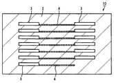
적층 부품의 일례로서, 적층 인덕터는, 코일 패턴을 인쇄한 자성체(페라이트) 시트를 일체적으로 적층한 후, 소성(燒成)함으로써 제작된다. 적층 인덕터는 신뢰성이 우수한 구조를 가지고, 누설 자속(leakage flux)이 적은 이점이 있지만, 일체적인 구조이므로, 코일 패턴으로 여자(勵磁) 전류를 흘렸을 때 발생하는 직류 자계에 의해 자성체가 부분적으로 자기 포화(magnetization)되어 인덕턴스가 급격하게 저하되는 문제가 있다. 이와 같은 적층 인덕터는 직류 중첩 특성이 뒤떨어지는 것으로 알려져 있다.As an example of a laminated component, a laminated inductor is produced by integrally laminating a magnetic body (ferrite) sheet printed with a coil pattern, and then firing the laminate. The multilayer inductor has an excellent reliability structure and has a low leakage flux. However, since the multilayer inductor is a monolithic structure, the magnetic body is partially magnetized by a direct current magnetic field generated when the excitation current flows through the coil pattern. There is a problem that the inductance is sharply lowered due to saturation (magnetization). Such multilayer inductors are known to be inferior in DC superposition characteristics.
이 문제를 해결하기 위하여, 도 47에 나타낸 바와 같이, 일본국 특개소 56-155516호 및 일본국 특개 2004-311944호는, 자기 갭층을 자성체층 사이에 설치하여 개자로(開磁路) 구조로 한 적층 인덕터(50)를 개시하고 있다. 이 적층 인덕터(50)는, 복수개의 자성체(페라이트)층(41)과 코일 패턴층(43)을 적층하여 형성되고, 자로에는 비자성체로 이루어지는 자기 갭층(44)이 삽입되어 있다. 도면 중, 자속의 흐름을 모식화하여 화살표로 나타낸다. 저여자(低勵磁) 전류 시에는, 자기 갭층(44)에 의해 분리된 각각의 영역에서, 코일 패턴(43)을 주회(周回)하는 자속 Φ a, 및 복수개의 코일 패턴(43)을 주회하는 자속 Φb가 형성된다. 대부분의 자속은 자기 갭층(44)을 통과하지 않고, 자기 갭층(44)을 경계로 하여 각각의 영역에서 자속의 경로가 형성되고, 마치 1개의 소자에서 2개의 인덕터가 직렬 접속된 것처럼 된다. 한편, 고여자 전류 시에는 코일 패턴(43) 사이의 자성체 부분이 자기 포화하고, 대부분의 자속은 자속 Φc와 같이 자기 갭층(44)을 통과하여 복수개의 코일 패턴을 주회하게 되어, 반자계에 의해 저여자 전류 시와 비교하여 인덕턴스값이 저하되지만, 용이하게 자기 포화되지 않는다. 따라서, 이와 같은 종래의 적층 인덕터에서는, 자기 갭층에 의해 직류 중첩 특성은 개선되지만, 근소한 여자 전류의 증가에 의해 인덕턴스값은 크게 변동한다. 또한, 자기 갭층(44)을 설치하지 않는 경우와 비교하면 직류 중첩 특성은 개선되지만, 대여자 전류에서의 사용에 대응할 수 있도록 새로운 개선이 요구되고 있다.In order to solve this problem, as shown in Fig. 47, Japanese Patent Laid-Open No. 56-155516 and Japanese Patent Laid-Open No. 2004-311944 have a magnetic gap layer interposed between magnetic material layers to form an open circuit structure. One
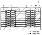
일본국 특개 2004-311944호는, 도 48에 나타낸 바와 같이, 코일 패턴의 중앙 부분에 자기 갭층(44)을 매립하고, 코일 패턴의 주위에 비자성체(47)를 매립한 적층 인덕터(50)를 개시하고 있다. 대부분의 자속이 자기 갭층(44)을 통과하므로, 이 적층 인덕터(50)는 저여자 전류로부터 고여자 전류까지 안정된 인덕턴스 값을 부여하지만, 대여자 전류에서의 성능이 불충분하고, 또한, 구조가 복잡하며 제조가 곤란하다.As shown in FIG. 48, Japanese Patent Laid-Open No. 2004-311944 discloses a
[발명이 해결하려고 하는 과제][Problems that the invention tries to solve]
따라서, 본 발명의 목적은, 저여자 전류로부터 고여자 전류까지 안정된 인덕턴스값을 얻을 수 있고, 우수한 직류 중첩 특성을 가지며, 용이하게 제조 가능한 적층 부품, 및 이것을 사용한 모듈을 제공하는 것이다.Accordingly, an object of the present invention is to provide a laminated component which can obtain a stable inductance value from a low excitation current to a high excitation current, has excellent direct current superimposition characteristics, and can be easily manufactured, and a module using the same.
[과제를 해결하기 위한 수단][MEANS FOR SOLVING THE PROBLEMS]
전술한 목적을 감안하여 연구한 결과, 본 발명자 등은, 적층 부품 내에 코일 패턴을 가지는 적층 부품에서, 상기 코일 패턴에 접하는 영역에 자기 갭층을 복수개 형성함으로써, 큰 여자 전류에서도 자성체부에서의 자기 포화가 쉽게 일어나지 않게 되고, 또한 와전류(渦電流) 손실을 저감할 수 있는 것을 발견하고, 본 발명에 도달했다.In view of the above-described object, the present inventors have found that, in a laminated component having a coil pattern in the laminated component, a plurality of magnetic gap layers are formed in a region in contact with the coil pattern, so that the magnetic saturation in the magnetic body portion is achieved even at a large exciting current. The present invention has been found to be difficult to occur and to reduce the eddy current loss.
즉, 본 발명의 적층 부품은, 자성체층 및 코일 패턴을 교대로 적층하고, 상기 코일 패턴을 적층 방향으로 접속하여 코일을 구성하여 이루어지고, 상기 코일 패턴에 접하는 영역에 자기 갭층이 복수개 형성되어 있는 것을 특징으로 한다.That is, the laminated component of the present invention is formed by alternately stacking a magnetic layer and a coil pattern, connecting the coil patterns in a stacking direction to form a coil, and a plurality of magnetic gap layers are formed in a region in contact with the coil pattern. It is characterized by.
상기 자기 갭층은 적층 방향으로 인접하는 적어도 2개의 코일 패턴으로 형성되어 있는 것이 바람직하다. 한쪽의 코일 패턴이 발생하는 자속은, 거기에 접하는 자기 갭층을 통과하지만, 다른 쪽의 코일 패턴에 접하는 자기 갭층을 쉽게 통과할 수 없기 때문에, 그 코일 패턴을 주회한다. 인접하는 2개의 코일 패턴 사이의 자성체부에서는, 각각의 코일 패턴에서 생긴 자속이 서로 캔슬되기 때문에, 큰 여자 전류에서도 자기 포화가 쉽게 일어나지 않는다.It is preferable that the magnetic gap layer is formed of at least two coil patterns adjacent in the stacking direction. The magnetic flux generated by one coil pattern passes through the magnetic gap layer in contact with it, but cannot travel easily through the magnetic gap layer in contact with the other coil pattern. In the magnetic body portion between two adjacent coil patterns, since the magnetic fluxes generated in the respective coil patterns are canceled with each other, magnetic saturation does not easily occur even with a large excitation current.
자기 갭층이 설치된 상기 코일 패턴의 개수는, 상기 코일의 턴(turn)수의 60% 이상인 것이 바람직하다. 상기 코일은, 0.75턴 이상의 코일 패턴을, 2턴 이상이 되도록 접속하여 이루어지는 것이 바람직하다. 적어도 일부의 코일 패턴의 권취수는 1턴을 초과하는 것이 바람직하다. 코일 패턴은 Ag, Cu 등의 저융점 금속이나 그 합금으로 형성되는 것이 바람직하다. 각 코일 패턴의 턴수가 0.75턴 미만이면, 코일 패턴 담지층의 적층수가 너무 증가한다. 특히 0.5턴 미만이면 적층 방향으로 인접하는 코일 패턴의 간격이 너무 커진다. 그리고, 코일의 인출부 등을 구성하는 일부의 코일 패턴은, 0.75턴 미만이라도 상관없다.It is preferable that the number of the said coil patterns provided with the magnetic gap layer is 60% or more of the number of turns of the said coil. The coil is preferably formed by connecting a coil pattern of 0.75 turns or more to be 2 turns or more. It is preferable that the winding number of at least one coil pattern exceeds 1 turn. The coil pattern is preferably formed of a low melting point metal such as Ag or Cu or an alloy thereof. If the number of turns of each coil pattern is less than 0.75 turns, the number of laminations of the coil pattern carrying layer will increase too much. In particular, if it is less than 0.5 turn, the spacing of the coil patterns adjacent in the stacking direction becomes too large. And some coil patterns which comprise the lead part of a coil etc. may be less than 0.75 turn.
적어도 일부의 코일 패턴을 1턴 초과로 하면, 코일 패턴 담지층의 개수를 줄일 수 있다. 권취수가 1턴을 넘으면, 필연적으로 코일 패턴을 형성하는 면적이 증가하고, 자로 단면적이 감소하지만, 동일 자성체 기판층 상에서 인접하는 코일 패턴 사이에도 자기 갭층을 형성함으로써, 1턴 이하의 코일 패턴으로 구성한 경우와 같은 정도 이상의 인덕턴스값을 얻을 수 있다. 다만, 자로 단면적의 감소에 의해 자기 포화가 용이해지고, 동일 자성체 기판층 상에서 대향하는 패턴 사이에서의 부유 용량의 증가에 의해 공진 주파수가 저하되고, 코일의 품질 계수 Q도 저하된다. 그러므로, 예를 들면, 적층 부품의 외형 치수가 3216 사이즈이면, 각 층에서의 코일 패턴은 3턴 이하로 하는 것이 바람직하다.If at least part of the coil pattern is more than one turn, the number of coil pattern bearing layers can be reduced. When the number of turns exceeds one turn, the area inevitably forming the coil pattern increases and the cross-sectional area is reduced. However, the magnetic gap layer is formed between adjacent coil patterns on the same magnetic substrate layer, thereby forming a coil pattern of one turn or less. Inductance values higher than those in the case can be obtained. However, magnetic saturation is facilitated by reducing the cross-sectional area of the magnetic domain, and the resonance frequency is lowered by the increase of the stray capacitance between the opposing patterns on the same magnetic substrate layer, and the quality factor Q of the coil is also lowered. Therefore, for example, when the external dimension of a laminated component is 3216 size, it is preferable that the coil pattern in each layer shall be 3 turns or less.
상기 자기 갭층은, 비자성재 또는 비투자율(比透磁率) 1∼5의 저투자율재로 이루어지는 것이 바람직하다. 상기 코일 패턴의 두께 t1에 대한 상기 자기 갭층의 두께 t2의 비 t2/t1 는 1 이하인 것이 바람직하고, 0.2 내지 1인 것이 보다 바람직하다.It is preferable that the said magnetic gap layer consists of a nonmagnetic material or the low permeability material of specific permeability 1-5. It is preferable that ratio t2 / t1 of thickness t2 of the said magnetic gap layer with respect to thickness t1 of the said coil pattern is 1 or less, and it is more preferable that it is 0.2-1.
적어도 일부의 코일 패턴이 이와 같은 구성을 가짐으로써, 적층 부품의 직류 중첩 특성이 개선된다. 모든 코일 패턴에 접하여 자기 갭층을 형성하면, 저여자 전류로부터 고여자 전류까지 안정된 인덕턴스값을 얻을 수 있고, 또한, 인덕턴스값이 쉽게 저하하지 않는, 우수한 직류 중첩 특성을 발휘할 수 있다.By the at least one coil pattern having such a structure, the DC superposition characteristic of a laminated component improves. By forming the magnetic gap layer in contact with all the coil patterns, a stable inductance value can be obtained from the low excitation current to the high excitation current, and the excellent direct current superimposition characteristic can be exhibited in which the inductance value does not easily decrease.
상기 자기 갭층 및 상기 코일 패턴을 상기 자성체 기판층 상에 중첩되지 않도록 형성해도 되고, 중첩되도록 형성해도 된다. 어느 경우도, 자기 갭층은 코일 패턴과 접하고, 코일 패턴의 근방에 생기는 자속은, 같은 자성체 기판층에 설치된 자기 갭층을 통과하고, 각 코일 패턴의 주위의 자성체(자성체 기판층 및 자성체 충전층)를 흘러서, 주회하는 루프를 형성한다.The magnetic gap layer and the coil pattern may be formed so as not to overlap on the magnetic substrate layer, or may be formed so as to overlap. In either case, the magnetic gap layer is in contact with the coil pattern, and the magnetic flux generated in the vicinity of the coil pattern passes through the magnetic gap layer provided on the same magnetic substrate layer and passes the magnetic bodies (magnetic substrate layer and magnetic filler layer) around each coil pattern. Flows, forming a loop around it.
자기 갭층은 적어도 1개의 자성체 영역을 가지는 것이 바람직하다. 자기 갭층에 설치되는 자성체 영역은, 적층 방향으로 인접하는 코일 패턴 사이의 자성체층보다 저여자 전류로 자기 포화되도록 설정한 면적 및 자기 특성을 가진다. 이와 같은 구성에 의해, 저여자 전류 시에는 높은 인덕턴스 값이 얻어지고, 고여자 전류 시에는 인덕턴스값은 저하되지만, 상기 자성체 영역과 자기 갭층이 일체적인 자기 갭으로서 기능하므로, 안정된 인덕턴스값을 얻을 수 있다.The magnetic gap layer preferably has at least one magnetic region. The magnetic region provided in the magnetic gap layer has an area and magnetic characteristics set so as to be magnetically saturated with a low excitation current than the magnetic layers between the coil patterns adjacent in the stacking direction. With such a configuration, a high inductance value is obtained at low excitation currents, and an inductance value decreases at high excitation currents, but the magnetic region and the magnetic gap layer function as an integral magnetic gap, so that a stable inductance value can be obtained. have.
적층 부품은, 자성체층, 코일 패턴 및 자기 갭층의 소결 수축 차이나 열팽창 차이에 의한 응력이나, 실장되는 회로 기판의 굴곡에 의한 응력 등을 받는다. 자성체층의 자기 특성은 응력 불균일에 의해 열화되므로, 응력에 의한 투자율 변화가 작은(내응력 특성이 우수하한) Li계 페라이트를 사용하는 것이 바람직하다. 이에 따라, 응력에 의한 인덕턴스값의 변동이 작은 적층 부품을 얻을 수 있다.The laminated component is subjected to stress due to sintering shrinkage difference or thermal expansion difference between the magnetic layer, coil pattern, and magnetic gap layer, stress due to bending of the circuit board to be mounted. Since the magnetic properties of the magnetic layer deteriorate due to stress unevenness, it is preferable to use Li-based ferrite having a small change in permeability due to stress (which is excellent in stress resistance). Thereby, the laminated component with little fluctuation | variation in the inductance value by stress can be obtained.
본 발명의 모듈의 일례는, 상기 적층 부품을, 내부에 컨덴서를 구비한 유전체 기판에 스위칭 소자를 포함하는 반도체 부품과 함께 실장한 것을 특징으로 한다. 본 발명의 모듈의 다른 예는, 상기 적층 부품을, 수지 기판에 스위칭 소자를 포함하는 반도체 부품과 함께 실장한 것을 특징으로 한다. 본 발명의 모듈의 또 다른 예는, 상기 적층 부품에 스위칭 소자를 포함하는 반도체 부품을 실장한 것을 특징으로 한다.One example of the module of the present invention is characterized in that the laminated component is mounted together with a semiconductor component including a switching element on a dielectric substrate having a capacitor therein. Another example of the module of the present invention is characterized in that the laminated component is mounted on a resin substrate together with a semiconductor component including a switching element. Another example of the module of the present invention is characterized in that a semiconductor component including a switching element is mounted on the laminated component.
[발명의 효과][Effects of the Invention]
상기 모노리식 구조를 가지는 본 발명의 적층 부품은, 우수한 직류 중첩 특성을 가지고, 이것을 사용한 DC-DC 컨버터는 높은 변환 효율을 가지며, 대전류에 대해서도 사용할 수 있다. 그러므로, 본 발명의 적층 부품을 가지는 DC-DC 컨버터는, 전지를 사용하는 휴대형의 각종 전자 기기(휴대 전화기, 휴대 정보 단말기 PDA, 노트북형 퍼스널 컴퓨터, 휴대형 뮤직/비디오 플레이어, 디지털 카메라, 디지털 비디오 카메라 등)에 유용하다.The laminated component of the present invention having the monolithic structure has excellent direct current superimposition characteristics, and the DC-DC converter using the same has high conversion efficiency and can be used for high current. Therefore, the DC-DC converter having the laminated component of the present invention is a portable electronic device using a battery (mobile phone, portable information terminal PDA, laptop personal computer, portable music / video player, digital camera, digital video camera). Etc.)
도 1은 본 발명의 제1 적층 부품의 일례의 외관을 나타낸 사시도이다.1 is a perspective view showing an appearance of an example of a first laminated part of the present invention.
도 2는 본 발명의 제1 적층 부품의 일례를 나타낸 단면도이다.2 is a cross-sectional view showing an example of the first laminated component of the present invention.
도 3은 본 발명의 제1 적층 부품의 일례의 자속의 흐름을 나타내는 모식도이다.It is a schematic diagram which shows the flow of the magnetic flux of an example of the 1st laminated component of this invention.
도 4는 본 발명의 제1 적층 부품의 일례를 나타낸 분해사시도이다.4 is an exploded perspective view showing an example of the first laminated component of the present invention.
도 5a는 본 발명의 제1 적층 부품의 일례에 사용되는 자성체층을 나타낸 평면도이다.5A is a plan view showing a magnetic layer used in one example of the first laminated component of the present invention.
도 5b는 본 발명의 제1 적층 부품의 일례에 사용되는 자성체층을 나타낸 단 면도이다.Fig. 5B is a cutaway view showing the magnetic layer used in one example of the first laminated component of the present invention.
도 6a는 본 발명의 제1 적층 부품의 일례에 사용되는 다른 자성체층을 나타낸 평면도이다.It is a top view which shows the other magnetic body layer used for an example of the 1st laminated component of this invention.
도 6b는 본 발명의 제1 적층 부품의 일례에 사용되는 다른 자성체층을 나타낸 단면도이다.6B is a cross-sectional view showing another magnetic layer used in one example of the first laminated component of the present invention.
도 7은 본 발명의 제1 적층 부품의 다른 예를 나타낸 단면도이다.7 is a cross-sectional view showing another example of the first laminated component of the present invention.
도 8은 본 발명의 제1 적층 부품의 다른 예에서의 자속의 흐름을 나타내는 모식도이다.It is a schematic diagram which shows the flow of a magnetic flux in the other example of the 1st laminated component of this invention.
도 9는 본 발명의 제2 적층 부품에서의 자속의 흐름을 나타내는 모식도이다.It is a schematic diagram which shows the flow of the magnetic flux in the 2nd laminated component of this invention.
도 10a는 본 발명의 제2 적층 부품에 사용하는 다른 자성체층을 나타낸 평면도이다.It is a top view which shows the other magnetic body layer used for the 2nd laminated component of this invention.
도 10b는 본 발명의 제2 적층 부품에 사용하는 다른 자성체층을 나타낸 단면도이다.It is sectional drawing which shows the other magnetic body layer used for the 2nd laminated component of this invention.
도 11은 본 발명의 제3 적층 부품에서의 자속의 흐름을 나타내는 모식도이다.It is a schematic diagram which shows the flow of the magnetic flux in the 3rd laminated component of this invention.
도 12a는 본 발명의 제3 적층 부품에 사용하는 다른 자성체층을 나타낸 평면도이다.It is a top view which shows the other magnetic body layer used for the 3rd laminated component of this invention.
도 12b는 본 발명의 제3 적층 부품에 사용하는 다른 자성체층을 나타낸 단면도이다.It is sectional drawing which shows the other magnetic body layer used for the 3rd laminated component of this invention.
도 13은 본 발명의 제4 적층 부품을 나타낸 단면도이다.It is sectional drawing which shows the 4th laminated part of this invention.
도 14a는 본 발명의 제4 적층 부품에 사용되는 다른 자성체층을 나타낸 평면도이다.14A is a plan view showing another magnetic layer used for the fourth laminated part of the present invention.
도 14b는 본 발명의 제4 적층 부품에 사용되는 다른 자성체층을 나타낸 단면도이다.14B is a cross-sectional view showing another magnetic layer used for the fourth laminated part of the present invention.
도 15는 본 발명의 제4 적층 부품에서의 자속의 흐름을 나타낸 모식도이다.It is a schematic diagram which shows the flow of the magnetic flux in the 4th laminated component of this invention.
도 16은 종래의 적층 부품, 및 본 발명의 제1 적층 부품 및 제4 적층 부품의 직류 중첩 특성을 나타낸 그래프이다.FIG. 16 is a graph showing a conventional laminated component and direct current superimposition characteristics of the first laminated component and the fourth laminated component of the present invention. FIG.
도 17은 본 발명의 제4 적층 부품의 다른 예를 나타낸 단면도이다.It is sectional drawing which shows the other example of the 4th laminated part of this invention.
도 18은 본 발명의 제4 적층 부품에 사용되는 다른 자성체층을 나타낸 평면도이다.18 is a plan view showing another magnetic layer used for the fourth laminated part of the present invention.
도 19는 본 발명의 제4 적층 부품에 사용되는 다른 자성체층을 나타낸 평면도이다.Fig. 19 is a plan view showing another magnetic layer used for the fourth laminated part of the present invention.
도 20은 본 발명의 제5 적층 부품을 나타낸 단면도이다.20 is a cross-sectional view illustrating a fifth laminated component of the present invention.
도 21a는 본 발명의 제5 적층 부품에 사용되는 다른 자성체층을 나타낸 평면도이다.Fig. 21A is a plan view showing another magnetic layer used for the fifth laminated part of the present invention.
도 21b는 본 발명의 제5 적층 부품에 사용되는 다른 자성체층을 나타낸 단면도이다.21B is a cross-sectional view showing another magnetic layer used for the fifth laminated component of the present invention.
도 22는 본 발명의 제5 적층 부품에서의 자속의 흐름을 나타내는 모식도이다.It is a schematic diagram which shows the flow of a magnetic flux in the 5th laminated component of this invention.
도 23은 본 발명의 제6 적층 부품을 나타낸 단면도이다.It is sectional drawing which shows the 6th laminated part of this invention.
도 24a는 본 발명의 제6 적층 부품에 사용되는 다른 자성체층을 나타낸 평면도이다.24A is a plan view showing another magnetic layer used for the sixth laminated part of the present invention.
도 24b는 본 발명의 제6 적층 부품에 사용되는 다른 자성체층을 나타낸 단면도이다.24B is a cross-sectional view showing another magnetic layer used for the sixth laminated part of the present invention.
도 25는 본 발명의 제7 적층 부품을 나타내는 분해사시도이다.25 is an exploded perspective view showing a seventh laminated part of the present invention.
도 26은 본 발명의 제7 적층 부품을 나타낸 단면도이다.It is sectional drawing which shows the 7th laminated part of this invention.
도 27은 본 발명의 제8 적층 부품을 나타낸 단면도이다.27 is a cross-sectional view showing an eighth laminated part of the present invention.
도 28은 본 발명의 제8 적층 부품의 다른 예를 나타낸 단면도이다.It is sectional drawing which shows the other example of the 8th laminated component of this invention.
도 29는 본 발명의 제8 적층 부품의 다른 예를 나타낸 단면도이다.It is sectional drawing which shows the other example of the 8th laminated component of this invention.
도 30은 본 발명의 제9 적층 부품의 외관을 나타낸 사시도이다.It is a perspective view which shows the external appearance of the 9th laminated component of this invention.
도 31은 본 발명의 제9 적층 부품의 등가 회로를 나타낸 도면이다.31 is a diagram showing an equivalent circuit of the ninth laminated component of the present invention.
도 32는 본 발명의 제9 적층 부품을 나타낸 분해사시도이다.32 is an exploded perspective view showing a ninth laminated part of the present invention.
도 33은 본 발명의 제9 적층 부품의 다른 예를 나타낸 분해사시도이다.33 is an exploded perspective view showing another example of the ninth laminated part of the present invention.
도 34는 본 발명의 모듈의 외관을 나타낸 사시도이다.34 is a perspective view showing the appearance of the module of the present invention.
도 35는 본 발명의 모듈을 나타낸 단면도이다.35 is a cross-sectional view showing a module of the present invention.
도 36은 본 발명의 모듈의 회로를 나타낸 블록도이다.36 is a block diagram illustrating a circuit of a module of the present invention.
도 37은 본 발명의 모듈의 다른 예의 회로를 나타낸 블록도이다.37 is a block diagram showing a circuit of another example of the module of the present invention.
도 38은 본 발명의 제1 적층 부품의 제조 방법을 설명하는 평면도이다.It is a top view explaining the manufacturing method of the 1st laminated component of this invention.
도 39는 본 발명의 제1 적층 부품의 직류 중첩 특성을 나타낸 그래프이다.39 is a graph showing the direct current superimposition characteristic of the first laminated part of the present invention.
도 40은 DC-DC 변환 효율의 측정 회로를 나타낸 도면이다.40 is a diagram illustrating a circuit for measuring DC-DC conversion efficiency.
도 41는 본 발명의 제1 적층 부품의 다른 예의 직류 중첩 특성을 나타낸 그래프이다.It is a graph which shows the DC superposition characteristic of the other example of the 1st laminated component of this invention.
도 42는 본 발명의 제2 적층 부품의 직류 중첩 특성을 나타낸 그래프이다.It is a graph which shows the DC superposition characteristic of the 2nd laminated component of this invention.
도 43은 본 발명의 제3 적층 부품의 직류 중첩 특성을 나타낸 그래프이다.43 is a graph showing the direct current superimposition characteristic of the third laminated part of the present invention.
도 44는 본 발명의 제4 적층 부품의 직류 중첩 특성을 나타낸 그래프이다.44 is a graph showing the direct current superimposition characteristic of the fourth laminated component of the present invention.
도 45는 본 발명의 제3 적층 부품의 다른 예의 직류 중첩 특성을 나타낸 그래프이다.It is a graph which shows the direct current superposition characteristic of the other example of the 3rd laminated component of this invention.
도 46은 본 발명의 제3 적층 부품의 다른 예의 직류 중첩 특성을 나타낸 그래프이다.It is a graph which shows the direct current superposition characteristic of the other example of the 3rd laminated component of this invention.
도 47은 종래의 적층 인덕터의 일례를 나타낸 단면도이다.47 is a cross-sectional view showing an example of a conventional multilayer inductor.
도 48은 종래의 적층 인덕터의 다른 일례를 나타낸 단면도이다.48 is a cross-sectional view showing another example of a conventional multilayer inductor.
본 발명의 적층 부품 및 모듈을 이하 상세하게 설명한다.The laminated component and module of the present invention will be described in detail below.
[1] 제1 적층 부품[1] first laminated parts
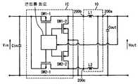
도 1은 본 발명의 제1 적층 부품의 일례로서의 적층 인덕터(10)의 외관 및 그 내부 구조를 나타내고, 도 2는 도 1의 적층 인덕터(10)의 단면을 나타내며, 도 3은 도 1의 적층 인덕터(10)에서의 자계 분포를 나타내고, 도 4는 도 1의 적층 인덕터(10)를 구성하는 각 층을 나타낸다.FIG. 1 shows the appearance and internal structure of the
(1) 적층 부품의 구조(1) structure of laminated parts
적층형 인덕터(10)는 11층(S1∼S11)으로 구성되며, 코일 패턴(3)이 형성된 자성체 기판층(2)으로 이루어지는 7개의 코일 패턴 담지층(1a∼1d)을 가지는 코일 형성역(1)과, 코일 형성역(1)의 상하에 각각 설치된 코일 패턴을 갖지 않는 2개의 자성체 기판층(2)으로 이루어지는 자성체역(5)을 가진다. 코일 형성역(1)에서는, 0.5턴∼1턴의 코일 패턴(3)(3a∼3d)은, 스루홀(6)을 통하여 접속되고, 6.5턴의 코일을 형성하고 있다. 코일의 양단은 적층 부품의 대향 측면에 인출되고, Ag 등의 도체 페이스를 눌어붙인 외부 전극(200a, 200b)과 접속되어 있다. 도 2에 나타낸 바와 같이, 코일 패턴(3)의 내측으로 그것과 접하는 영역에 자기 갭층(4)이 형성되어 있다. 적층형 인덕터(10)는 LTCC(Low-Temperature Co-fired Ceramics)법에 의해 형성되는 것이 바람직하다.The stacked
각 코일 패턴 담지층(1a∼1d)은, 예를 들면, 소프트 페라이트의 페이스트를 사용하여 닥터 블레이드법, 칼렌다 롤(calendar roll)법 등에 의해 자성체 기판층(2)용의 그린 시트를 성형하고, 그 위에 Ag, Cu 또는 이들을 포함하는 합금의 도전 페이스트를 소정의 코일 패턴(3a∼3d)에 인쇄 또는 도포하고, 또한 자기 갭층(4)이 되는 비자성체 페이스트를 소정의 영역에 인쇄 또는 도포한 후, 자기 갭층(4)을 덮고, 또한 코일 패턴의 상면과 실질적으로 같은 높이가 되도록, 코일 패턴을 제외한 영역에 자성체 페이스트를 인쇄 또는 도포하고, 자성체 충전층(2a∼2d)을 형성한다. 자성체 충전층(2a∼2d)은 자성체 기판층(2) 상의 코일 패턴(3a∼3d)의 형상에 따라 상이한 형상을 가진다. 자성체역(5)을 구성하는 각 자성체 기판층(2)은 전술한 바와 동일한 그린 시트로 이루어진다. 복수개(7개)의 코일 패턴 담지층(1a∼1d)을 적층하여, 코일 패턴(3a∼3d)을 스루홀(6)에서 접속하여 코일로 한 후, 그 양측에 각각 1개 이상(2개)의 자성체 기판층(2)을 도 4에 나타낸 바와 같이 적층하고, 1100℃ 이하의 온도로 소결하는 것이 바람직하다. 외부 전극(200a, 200b)을 구성하는 도전 재료는 특히 한정되지 않고, Ag, Pt, Pd, Au, Cu, Ni 등의 금속 또는 이들 합금을 사용할 수 있다.Each coil
도 4에 나타낸 각 코일 패턴 담지층(1a∼1d)은 코일 패턴(3a∼3d) 및 자성체 충전층(2a∼2d)의 형상이 상이한 점 외에, 동일한 구조를 가지므로, 예를 들면, 코일 패턴 담지층(1b)을 도 5a 및 도 5b에 의해 상세하게 설명한다. 이 설명은 다른 코일 패턴 담지층에도 그대로 적용될 수 있다. 코일 패턴 담지층(1b)은, 예를 들면, Li-Mn-Zn 페라이트 분말, 폴리비닐부티랄을 주성분으로 하는 유기 바인더, 및 에탄올, 톨루엔, 크실렌 등의 용매를 볼 밀(ball mill) 내에서 혼련하고, 얻어진 슬러리를 점도를 조제(調製)한 후, 폴리에스테르 필름 등의 캐리어 필름 상에 닥터 블레이드법 등으로 도포 및 건조하고, 얻어진 그린 시트(건조 두께: 15㎛∼60㎛)에 접속용의 스루홀을 뚫고, 도전 페이스트에 의해 코일 패턴(3b)을 10㎛∼30㎛의 두께로 인쇄하고, 또한 스루홀(6)에 도전 페이스트를 충전하고, 코일 패턴(3b)의 내측의 전체면을 덮도록 지르코니아 페이스트 등의 비자성체 페이스트(4)를 인쇄 또는 도포함으로써 자기 갭층(4)을 형성함으로써 얻어진다. 자기 갭층(4)의 두께는 3㎛ 이상이며 코일 패턴(3b)의 두께 이하인 것이 바람직하다.Each of the coil
자기 갭층(4)은, 자기 갭층용 페이스트로 코일 패턴(3b)의 내측을 포함하는 영역 전체를 덮고, 코일 패턴(3b)의 둘레부와 접하도록 형성된다. 또는, 개구부를 가지는 자기 갭층(4)을 인쇄한 후, 개구부에 코일 패턴(3b)을 인쇄해도 된다. 이 경우, 코일 패턴(3b)은 자기 갭층(4)의 둘레부를 덮는다. 어느 경우도, 소결 후의 각 코일 패턴(3)의 둘레부와 자기 갭층(4)의 둘레부는 실질적으로 접촉된 상태가 된다. 이와 같은 자기 갭층(4)이 적층 방향으로 중첩되어 배치되므로, 각 코일 패턴(3)에 의해 생기는 자속이, 다른 코일 패턴과 쇄교(鎖交)하는 것을 감소시킬 수 있다.The
자기 갭층(4)은 비자성재 또는 비투자율이 1∼5의 저투자율재에 의해 얇게 형성되는 것이 바람직하다. 저투자율재로 이루어지는 자기 갭층(4)은, 비자성재로 이루어지는 경우보다 두꺼워질 수 밖에 없지만, 인쇄 고정밀도에 의한 인덕턴스값의 불균일을 억제할 수 있다.The
저투자율재의 비투자율이 5보다 큰 경우, 자기 갭층(4)으로서의 기능이 저하된다. 비투자율 1∼5의 저투자율재는, 비자성 산화물(예를 들면, 지르코니아 등)의 분말에 자성체 분말을 혼합함으로써 얻어진다. 또한, 적층 부품의 사용 온도 범위보다 충분히 저온(예를 들면 -40℃ 이하)의 퀴리 온도를 가지는 Zn 페라이트를 사용해도 된다. Zn 페라이트는 소결 수축이 자성체 기판층(2)에 가깝다.When the specific permeability of the low permeability material is larger than 5, the function as the
자기 갭층(4)에 사용하는 비자성재 및 저투자율재로서는, ZrO2, B2O3-SiO2계 유리, Al2O3-SiO2계 유리 등의 유리 종류, Zn 페라이트, Li2O·Al2O3·4SiO2, Li2O·Al2O3·2SiO2, ZrSiO4, 3Al2O3·2SiO2, CaZrO3, SiO2, TiO2, WO3, Ta2O5, Nb2O5 등을 들 수 있다. 자기 갭층(4)용 페이스트는, 예를 들면, 지르코니아(ZrO2)의 분말, 에틸 셀룰로오스 등의 유기 바인더 및 용제를, 3개의 롤, 호모지나이저(homogenizer), 샌드 밀(sand mill) 등으로 혼련함으로써 조제한다. 적층 부품의 소결 온도에서는 치밀화(緻密化)하지 않는 지르코니아를 사용하면, 열팽창 계수의 차이에 의해 자성체 기판층(2)이 코일 패턴(3)으로부터 받는 압축 응력을 완화할 수 있고, 자성체 기판층(2)에 크랙(crack)이 발생하는 것을 방지할 수 있다. 자기 갭층(4)이 외면에 노출되어 있는 경우 등에 치밀화할 필요가 있을 때는, Zn, Cu, Bi 등의 산화물(예를 들면, Bi2O3)을 저온 소결 촉진 물질로서 첨가하는 것이 바람직하다.Examples of the nonmagnetic material and the low permeability material used for the
도 6a 및 도 6b는, 코일 패턴(3b)의 상면과 실질적으로 같은 높이가 되도록, 코일 패턴(3b)을 제외한 영역에 자성체 페이스트를 인쇄 또는 도포하여 이루어지는 자성체 충전층(2a)을 가지는 코일 패턴 담지층(1b)을 나타낸다. 자성체 페이스트는 그린 시트와 주성분 조성이 같은 페라이트 분말을 함유하는 것이 바람직하다. 다만, 페라이트 분말의 결정 입자 직경, 부성분의 종류, 첨가량 등은 상이해도 된다. 자성체 페이스트는 자성체 분말, 에틸 셀룰로오스 등의 바인더 및 용제를 배합하여 제작된다. 자성체 충전층(2a)을 설치함으로써, 예를 들면, 코일 패턴이 15㎛ 이상의 두께를 가지는 경우라도, 적층 압착 시의 적층 어긋남이나, 압착 후의 층간 박리(디라미네이션)의 발생을 저감할 수 있다.6A and 6B show a coil pattern bearing having a
자성체 기판층(2) 및 자성체 충전층(2a)에 사용하는 자성체 재료는, 예를 들면, 조성식: x(Li0.5FeO.5)O·yZnO·zFe2O3(단, x, y 및 z는 0.05≤x≤0.55, 0.05≤y≤0.40, 0.40≤z≤0.55, 및 x+y+z=1을 만족시킨다)에 의해 표현되는 주성분에 2 내지 30질량%의 Bi2O3를 첨가한 Li계 페라이트인 것이 바람직하다. 이 Li계 페라이트 는 800℃∼1000℃로 소성 가능하며, 저손실 및 고비저항이며, 각형비(角型比)가 작고, 응력 특성이 우수하다. ZnO의 일부를 CuO로 치환하면 저온 소결화가 진행되고, Fe203의 일부를 Mn2O3로 치환하면 비저항이 향상된다.Magnetic material using the
상기 Li계 페라이트 이외에, Ni계 페라이트, Mg계 페라이트 등의 소프트 페라이트를 사용할 수도 있다. 자성체 기판층(2) 및 자성체 충전층(2a)은, 코일 패턴, 자기 갭층, 외부 전극 등으로부터 응력을 받으므로, 응력에 의한 자기 특성의 변화가 작은 Li계 페라이트, Mg계 페라이트를 사용하는 것이 바람직하고, Li계 페라이트가 가장 바람직하다. 코어 로스(core loss)를 저감시키기 위해서는 Ni계 페라이트가 바람직하다.In addition to the above Li-based ferrites, soft ferrites such as Ni-based ferrites and Mg-based ferrites may be used. Since the
(2) 동작 원리(2) operating principle
본 발명의 적층 부품에서는, 각 코일 패턴(3)에 접하도록 설치된 자기 갭층(4)이 분산되어 있다. 종래부터 모든 자속이 복수개의 코일 패턴을 포함하는 루프를 그리는 것이 이상적이고, 각 코일 패턴의 주위의 작은 루프를 그리는 자속은 단지 인덕턴스값을 저하시키는 누설 자속인 것으로 여겨져 왔다. 그러나, 본 발명에서는, 도 3에 나타낸 바와 같이, 코일 패턴(3a, 3b)이 발생시키는 자속 Φa, Φa'(각 코일 패턴(3a, 3b)의 주위의 자성체(2) 및 각 자기 갭층(4a, 4b)을 돈다), 자속 Φb(코일 패턴(3a, 3b) 양쪽을 돈다), 및 자속 Φc(코일 패턴(3a, 3b) 및 다른 코일 패턴도 돈다) 중, 자속 Φb 및 Φc는 각 코일 패턴(3a, 3b)에 접하는 자기 갭층(4a, 4b)에 의해 저감되고, 거의 자속 Φa, Φa'만 남는다.In the laminated component of the present invention, the magnetic gap layers 4 provided to contact each
코일 패턴(3a) 주위의 자속 Φa와 코일 패턴(3b) 주위의 자속 Φa'는, 코일 패턴(3a, 3b) 사이의 자성체부를 자로로서 공유한다. 코일 패턴(3a, 3b) 사이의 자성체부에서는, 자속 Φa, Φa'의 방향이 반대이므로 직류 자계가 캔슬되고, 큰 인덕턴스는 얻을 수 없지만, 고여자 전류에서는 국부적인 자기 포화가 쉽게 생기지 않는다. 또한, 다른 코일 패턴과 교차하는 자속이 적으므로, 얻어지는 인덕턴스값은 각 코일 패턴(3)에서 얻어지는 인덕턴스값의 합산이 되고, 저여자 전류로부터 고여자 전류까지 안정되어 있다.The magnetic flux Φa around the
도 7은 코일 형성역(1)을 8층에 의해 구성한 적층 부품을 나타내고, 도 8은 이 적층 부품에서의 자속의 흐름을 모식적으로 나타낸다. 코일 패턴(3) 각각에 접하여 형성된 자기 갭층(4)에 의해, 층수의 다소에 관계없이, 코일 패턴(3)에 의해 생기는 자속 Φa는, 각 코일 패턴(3)을 주회한다.FIG. 7: shows the laminated component which comprised the coil formation area |
본 발명의 적층 부품에서는, 큰 루프를 그리는 자속이 줄어들고, 외부로의 누출 자속이 감소하였으므로, 코일 형성역(1)의 상하에 위치하는 자성체역을 얇게 할 수 있다. 또한, 1개의 적층 부품에 복수개의 코일을 설치한 인덕터 어레이에서는, 코일 사이의 자기 결합을 저감시킬 수 있다.In the laminated component of the present invention, the magnetic flux drawing the large loop is reduced, and the magnetic flux leaking out to the outside is reduced, so that the magnetic body region located above and below the
[2] 제2 적층 부품[2] second laminated components
도 9는 제2 적층 부품의 단면을 나타내고, 도 10a 및 도 10b는 이 적층 부품에 사용하는 코일 패턴 담지층을 나타낸다. 이 적층 부품은, 제1 적층 부품과 거의 같은 구성이므로, 상이한 부분을 설명하고, 중복되는 부분의 설명은 생략한다.FIG. 9 shows a cross section of the second laminated component, and FIGS. 10A and 10B show a coil pattern carrying layer used for this laminated component. Since this laminated part has the structure substantially the same as a 1st laminated part, it demonstrates a different part and description of the overlapping part is abbreviate | omitted.
코일 패턴 담지층(1b)은, 자성체 기판층(2) 상에 형성된 코일 패턴(3)과, 코 일 패턴(3)에 접하여 그 외측 영역의 전체를 덮는 자기 갭층(4)과, 코일 패턴(3)의 내측 영역에 형성된 자성체 충전층(2a)을 가진다. 도 10a는, 구성을 명확하게 하기 위하여, 자기 갭층(4)을 덮는 자성체 충전층(2a)이 형성되기 전의 상태를 나타내고, 도 10b는 자성체 충전층(2a)을 형성한 후의 상태를 나타낸다. 이후의 설명에서도 마찬가지이다. 제2 적층 부품은, 각 코일 패턴(3)을 주회하는 자속이 자기 갭층(4)을 통과하고, 다른 코일 패턴과 쇄교하는 자속이 저감하고 있으므로, 우수한 직류 중첩 특성을 발휘한다.The coil
[3] 제3 적층 부품[3] laminated parts, third
도 11은 제3 적층 부품의 단면을 나타내고, 도 12a 및 도 12b는 이 적층 부품에 사용하는 코일 패턴 담지층을 나타낸다. 이 코일 패턴 담지층은, 코일 패턴(3b)의 내측 및 외측의 영역 전체를 덮는 자기 갭층(4)을 가지고, 코일 패턴(3)을 제외한 영역은 자성체 페이스트의 인쇄에 의해 자성체 충전층(2a)이 형성되어 있다[도 12b]. 제3 적층 부품은, 제1 적층 부품 및 제2 적층 부품과 비교하여 자기 갭이 길기 때문에, 인덕턴스값이 낮지만, 다른 코일 패턴과 쇄교하는 자속이 더욱 줄어들어 있으므로, 우수한 직류 중첩 특성을 발휘한다.FIG. 11: shows the cross section of a 3rd laminated component, and FIG. 12A and 12B show the coil pattern carrying layer used for this laminated component. The coil pattern carrying layer has a
[4] 제4 적층 부품[4] fourth laminated components
도 13은 제4 적층 부품의 단면을 나타내고, 도 14a 및 도 14b는 이 적층 부품에 사용하는 1개의 자성체층을 나타내고, 도 15는 이 적층 부품에서의 자계 분포를 나타낸다. 이 적층 부품에 사용하는 코일 패턴 담지층(1b)에는, 자기 갭층(4)의 개구부(14)에 자성체 충전층(2a)이 설치되어 있다. 개구부(14)는, 코일 패턴 사이의 자성체부로부터 저여자 전류로 자기 포화되도록, 개구 면적 및 충전하는 자성체의 자기 특성을 적절하게 선정되는 것이 바람직하다.FIG. 13: shows the cross section of a 4th laminated component, FIG. 14A and 14B show one magnetic body layer used for this laminated component, FIG. 15: magnetic field distribution in this laminated component. In the coil
도 16은, 종래의 적층 부품 (A), 제1 적층 부품 (B) 및 제4 적층 부품 (C)의 직류 중첩 특성을 나타낸다. 종래의 적층 부품은, 중앙에 1개소만 자기 갭층을 형성한, 도 47에 나타낸 적층 인덕터이다. 제4 적층 부품은, 개구부(14)를 통과하는 자속 Φc에 의해, 저여자 전류 시에는 제1 적층 부품보다 큰 인덕턴스값을 나타낸다. 이와 같은 직류 중첩 특성에 의해, 저여자 전류 시에 문제가 되는 전류 리플(current ripple)을 억제할 수 있다. 개구부(14) 내의 자성체 충전층이 자기 포화된 후, 개구부(14)는 자기 갭으로서 기능하므로, 자속 Φc가 감소하고, 제1 적층 부품과 같은 자계 분포가 된다. 그러므로, 고여자 전류까지 자기 포화가 쉽게 일어나지 않고, 종래의 적층 인덕터보다 우수한 직류 중첩 특성을 발휘한다.16 shows the direct current superimposition characteristic of the conventional laminated component (A), the first laminated component (B), and the fourth laminated component (C). The conventional laminated component is the laminated inductor shown in FIG. 47 in which only one magnetic gap layer is formed in the center. The fourth laminated component exhibits an inductance value larger than that of the first laminated component at the time of low excitation current due to the magnetic flux Φ c passing through the
제4 적층 부품에서는, 모든 자기 갭층에 개구부(14)를 설치하고 있지만, 도 17에 나타낸 바와 같이, 일부의 자기 갭층에만 개구부(14)를 설치해도 된다. 또한, 도 18 및 도 19에 나타낸 바와 같이, 1개의 자기 갭층에 복수개의 개구부(14)를 설치해도 되고, 그 형상, 위치, 면적 및 개수는 한정되지 않는다. 개구부(14)의 형상을 변경함으로써, 원하는 자기 특성을 가지는 적층 부품을 얻을 수 있다.In the fourth laminated component, the
[5] 제5 적층 부품[5] laminated parts
도 20은 제5 적층 부품의 단면을 나타내고, 도 21a 및 도 21b는 이 적층 부품에 사용하는 코일 패턴 담지층을 나타내고, 도 22는 이 적층 부품에서의 자계 분포를 나타낸다. 이 코일 패턴 담지층에는, 1층당 코일 패턴의 권취수가 1턴을 넘 고 있고, 동일 층에서 인접하는 패턴 사이에도 자기 갭층(4)이 설치되어 있다. 코일 패턴(3)의 주위에는, 작은 루프를 그리는 자속 Φa', Φa"와, 코일 패턴(3) 전체를 루프하는 자속 Φa가 형성된다. 동일 층 내의 코일 사이에서 자기적인 결합을 얻을 수 있으므로, 1턴으로 구성하는 것보다 큰 인덕턴스값을 얻을 수 있다.FIG. 20 shows a cross section of the fifth laminated component, FIGS. 21A and 21B show a coil pattern carrying layer used for this laminated component, and FIG. 22 shows a magnetic field distribution in this laminated component. In this coil pattern carrying layer, the number of turns of the coil pattern per layer exceeds one turn, and the
이 적층 부품에서도, 다른 층의 코일 패턴과 교차하는 자속은 줄일 수 있으므로, 큰 인덕턴스값을 얻으면서, 우수한 직류 중첩 특성을 얻을 수 있다. 또한, 코일 형성역(1)의 적층수를 삭감할 수 있으므로, 적층 부품을 저배화할 수 있다.Also in this laminated component, the magnetic flux crossing the coil pattern of another layer can be reduced, so that a high direct current superimposition characteristic can be obtained while obtaining a large inductance value. Moreover, since the number of lamination | stacking of the coil formation area |
[6] 제6 적층 부품[6] sixth laminated parts
도 23은 제6 적층 부품의 단면을 나타내고, 도 24a 및 도 24b는 이 적층 부품에 사용하는 코일 패턴 담지층을 나타낸다. 이 적층 부품에서도, 자기 갭층(4)의 일부에 형성된 개구부(14)는 자성체 충전층을 가진다. 이 적층 부품도, 큰 인덕턴스값을 가지면서, 우수한 직류 중첩 특성을 발휘한다.FIG. 23 shows a cross section of the sixth laminated part, and FIGS. 24A and 24B show the coil pattern carrying layer used for this laminated part. Also in this laminated part, the opening
[7] 제7 적층 부품[7] seventh laminated parts
도 25는 제7 적층 부품을 구성하는 각 층을 나타내고, 도 26은 그 단면도이다. 각 코일 패턴(3)의 권취수는 0.75턴이며, 적층 부품 전체에서는 4.5턴의 코일이 형성되어 있다. 그러므로, 코일 형성역(1) 중의 코일 패턴 담지층이 10층(S1∼Sl0)으로 제1 적층 부품보다 많다.FIG. 25: shows each layer which comprises the 7th laminated component, and FIG. 26 is sectional drawing. The number of turns of each
이 적층 부품은, 코일 형성역(1)의 최상층(S8) 및 최하층(S3)에 자기 갭층(4)을 갖지 않지만, 모든 중간층(S4∼S7)에 자기 갭층(4)을 가지고(코일의 턴수의 2/3에 해당된다), 우수한 직류 중첩 특성을 발휘한다.This laminated component does not have the
[8] 제8 적층 부품[8] eighth laminate parts
도 27∼도 29는 제8 적층 부품을 나타낸다. 제8 적층 부품은, 코일 패턴과 적층 방향으로 중첩되는 자기 갭층을 가진다. 도 27에 나타낸 적층 부품에서는 자기 갭층(4)은 코일 패턴(3)의 일부와 중첩되어 있고, 도 28에 나타낸 적층 부품에서는 자기 갭층(4)은 코일 패턴(3) 전체와 중첩되어 있고, 도 29에 나타낸 적층 부품에서는 자기 갭층(4)은 자성체 기판층(2)의 전체면을 덮고 있다. 제8 적층 부품에서도 자기 갭층(4)에 개구부(14)를 설치해도 된다. 이 경우, 자기 갭층(4) 두께만큼 적층 부품이 두꺼워지지만, 우수한 직류 중첩 특성을 얻을 수 있다.27 to 29 show an eighth laminated part. The eighth laminated part has a magnetic gap layer overlapping the coil pattern in the lamination direction. In the laminated component shown in FIG. 27, the
[9] 제9 적층 부품[9] 9th laminated components
도 30은 복수개의 인덕터를 가지는 적층 부품(인덕터 어레이)의 외관을 나타내고, 도 31은 그 등가 회로를 나타내며, 도 32 및 도 33은 그 내부 구조를 나타낸다. 이 적층 부품은, 적층된 코일 패턴(3)으로 이루어지는 코일에 중간 탭을 설치하여, 코일을 권취 방향이 상이한 2개의 코일로 분할한 것이며, 멀티 페이즈 DC-DC 컨버터에 사용된다.Fig. 30 shows the appearance of a laminated component (inductor array) having a plurality of inductors, Fig. 31 shows an equivalent circuit thereof, and Figs. 32 and 33 show the internal structure thereof. This laminated component is provided with an intermediate tab in a coil formed of the
이 적층 부품은 외부 단자(200a∼200c)를 구비하고, 외부 단자(200a)가 중간 탭이다. 외부 단자(200a와 200b) 사이에 인덕터 L1이 형성되고, 외부 단자(200a와 200c) 사이에 인덕터 L2가 형성된다. 도 32에 나타내는 적층 부품은, 각각 2.5턴의 코일로 형성된 인덕터 L1, L2를, 적층 방향으로 적층하여 구성하고 있다. 제9 적층 부품도, 전술한 실시형태와 마찬가지로 형성된 자기 갭층(4)을 구비하고 있으므로, 인덕터 L1, L2는 직류 중첩 특성이 우수하고, 나아가서는 코일 사이의 자기 결합을 저감할 수 있다.This laminated component includes
도 33에 나타낸 인덕터 어레이는, 각각 2.5턴의 코일로 형성된 인덕터 L1, L2를, 평면 방향으로 배열한 것이다. 이 경우도 우수한 직류 중첩 특성을 발휘한다. 그리고, 중간 탭을 설치하지 않고, 각각의 코일의 단부를 상이한 외부 단자와 접속해도 되고, 그 용도는 멀티 페이즈 DC-DC 컨버터로 한정되지 않는다.The inductor array shown in FIG. 33 arranges the inductors L1 and L2 formed from the coil of 2.5 turns, respectively, in the planar direction. This case also exhibits excellent DC superposition characteristics. And the edge part of each coil may be connected with a different external terminal, without providing an intermediate | middle tab, The use is not limited to a multi-phase DC-DC converter.
[10] DC-DC 컨버터 모듈[10] DC-DC converter modules
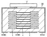
도 34는 본 발명의 적층 부품을 사용한 DC-DC 컨버터 모듈의 외관을 나타내고, 도 35는 그 단면을 나타내며, 도 36은 그 등가 회로를 나타낸다. 이 DC-DC 컨버터 모듈은, 인덕터를 내장한 적층 부품(10)에, 스위칭 소자 및 제어 회로를 포함하는 반도체 집적회로 부품 IC와 컨덴서 Cin, Cout를 실장한 강압형 DC-DC 컨버터이다. 적층 부품(10)의 배면에는 복수개의 외부 단자(90)가 형성되어 있고, 측면에 형성된 접속 전극에 의해 반도체 집적회로 부품 IC와, 인덕터 등과 접속되어 있다. 접속 전극은 적층 부품 내의 스루홀에서 형성해도 된다. 외부 단자(90)에 부여한 부호는 접속하는 반도체 집적회로 부품 IC의 단자에 대응하고, 외부 단자 Vcon은 출력 전압 가변 제어용 단자와, 외부 단자 Ven은 출력의 ON/OFF 제어용 단자와, 외부 단자 Vdd는 스위칭 소자를 ON/OFF 제어하기 위한 단자와, 외부 단자 Vin은 입력 단자와, 외부 단자 Vout은 출력 단자와 각각 접속한다. 외부 단자 GND는 그라운드 단자 GND와 접속한다.Fig. 34 shows the appearance of a DC-DC converter module using the laminated component of the present invention, Fig. 35 shows its cross section, and Fig. 36 shows its equivalent circuit. This DC-DC converter module is a step-down DC-DC converter in which a semiconductor integrated circuit component IC including a switching element and a control circuit, capacitors Cin, and Cout are mounted on a
적층 부품(10)은, 코일 패턴(3)과 접하도록 자기 갭층(4)이 형성되어 있으므로, 우수한 직류 중첩 특성을 발휘한다. 또한, 외부로의 누출 자속이 적기 때문 에, 반도체 집적회로 IC와 인덕터를 근접하여 배치해도, 반도체 집적회로 IC에 노이즈를 생기게 하지 않고, 우수한 변환 효율을 가지는 DC-DC 컨버터가 된다.Since the
DC-DC 컨버터 모듈은, 프린트 회로 기판에 적층 부품(10), 반도체 집적회로 IC 등을 실장해도, 컨덴서 Cin, Cout 등을 내장한 컨덴서 기판에 적층 부품(10), 반도체 집적회로 IC 등을 실장해도 얻어진다.The DC-DC converter module mounts the
DC-DC 컨버터 모듈의 다른 예로서, 도 37에 나타내는 등가 회로를 가지는 강압형 멀티 페이즈형의 DC-DC 컨버터 모듈이 있다. 입력 컨덴서 Cin, 출력 컨덴서 Cout, 출력 인덕터 L1, L2, 및 제어 회로 CC를 포함하는 반도체 집적회로 IC에 의해 구성된다. 출력 인덕터 L1, L2에 전술한 인덕터 어레이를 사용할 수 있고, 이 DC-DC 컨버터 모듈도 고여자 전류에 대응하고, 우수한 변환 효율을 발휘한다.As another example of the DC-DC converter module, there is a step-down multi-phase DC-DC converter module having an equivalent circuit shown in FIG. And a semiconductor integrated circuit IC including an input capacitor Cin, an output capacitor Cout, an output inductor L1, L2, and a control circuit CC. The inductor array described above can be used for the output inductors L1 and L2. The DC-DC converter module also responds to a high excitation current and exhibits excellent conversion efficiency.
이상, 적층 부품을 시트 적층법에 의해 제조하는 예를 나타냈으나, 도 38의 (a) 내지 (p)는 인쇄법에 의해 적층 부품을 제조하는 방법을 나타낸다. 본 발명의 적층 부품의 인쇄에 의한 제조법은, (a) 자성체 페이스트를 폴리에스테르 필름 등의 캐리어 필름 상에 인쇄·건조하여 제1 자성체층(2)을 형성하고, (b) 코일 패턴(3d)을 도전 페이스트로 인쇄하고, (c) 소정의 영역에 비자성체 페이스트를 인쇄하여 자기 갭층(4)을 형성하고, (d) 코일 패턴의 단부를 제외한 부분에 자성체 페이스트를 인쇄하여 제2 자성체층(2)을 형성하고, (e) 개구부(120)로부터 나타나는 코일 패턴(3d)과 중첩하여 도전 페이스트를 인쇄하여 코일 패턴(3a)을 형성하고, (f) 비자성체 페이스트를 인쇄하여 자기 갭층(4)을 형성하고, (g) 자성체 페이스트(2)를 인쇄하고, 이후 전술한 바와 같은 단계[(h)∼(p)]를 차례로 반복함으로써 이루어진다.As mentioned above, although the example which manufactures a laminated component by the sheet lamination method was shown, FIG.38 (a)-(p) shows the method of manufacturing a laminated component by the printing method. In the manufacturing method by printing the laminated component of the present invention, (a) the magnetic paste is printed and dried on a carrier film such as a polyester film to form the first
본 발명을 이하의 실시예에 의해 보다 상세하게 설명하지만, 본 발명은 이들에 한정되는 것은 아니다.The present invention is explained in more detail by the following examples, but the present invention is not limited thereto.
[실시예 1]Example 1
(1) 시료 A(실시예)의 제작(도 1∼도 6에 나타낸 제1 적층 부품)(1) Preparation of Sample A (Example) (First Laminated Part As Shown in Figs. 1 to 6)
49.0mol%의 Fe2O3, 13.0mol%의 CuO, 21.0mol%의 ZnO, 및 NiO를 잔여부로 하는 Ni-Cu-Zn계 페라이트(퀴리 온도 Tc: 240℃, 및 주파수 100kHz에서의 첫투자율: 300)의 가소 분말 100중량부에 대하여, 10중량부의 폴리비닐부티랄을 주성분으로 하는 유기 바인더, 가소제 및 용제를 더하여, 볼 밀로 혼련하여, 자성체 슬러리를 얻었다. 이 자성체 슬러리를 그린 시트에 성형하였다.Ni-Cu-Zn-based ferrites having 49.0 mol% Fe2 O3 , 13.0 mol% CuO, 21.0 mol% ZnO, and NiO as a remainder (Curie temperature Tc: 240 ° C., and frequency of 100 kHz: An organic binder, a plasticizer and a solvent containing 10 parts by weight of polyvinyl butyral as a main component were added to 100 parts by weight of the plastic powder of 300), and kneaded with a ball mill to obtain a magnetic slurry. This magnetic slurry was molded into a green sheet.
일부 그린 시트에 스루홀(6)을 형성하고, 스루홀(6)을 형성한 그린 시트 및 스루홀을 형성하고 있지 않은 그린 시트의 표면에, 자기 갭층(4)이 되는 비자성 지르코니아의 페이스트를 소정의 패턴으로 인쇄하고, 코일 패턴(3)이 되는 도전성 Ag 페이스트를 인쇄했다.The non-magnetic zirconia paste which becomes the
지르코니아 페이스트 인쇄층 및 Ag 페이스트 인쇄층에 의한 단차를 없애기 위하여, 이들을 인쇄하고 있지 않은 영역에 그린 시트와 같은 Ni-Cu-Zn 페라이트의 페이스트를 인쇄하고, 자성체 충전층(2a∼2d)을 형성하였다.In order to eliminate the step by the zirconia paste printed layer and the Ag paste printed layer, a paste of Ni-Cu-Zn ferrite such as a green sheet was printed on the areas where these were not printed, and magnetic filler layers 2a to 2d were formed. .
도 4에 나타낸 바와 같이, 자성체 기판층(2)에 지르코니아 페이스트 및 Ag 페이스트를 인쇄한 코일 패턴 담지층(1a∼1d)을 코일 패턴이 소정의 턴수로 되도록 적층하여 코일 형성역(1)을 형성하였다. 코일 형성역(1)의 상하로, 소정의 전체 사이즈가 되도록, 지르코니아 페이스트 및 Ag 페이스트가 인쇄되어 있지 않은 무지(無地)의 자성체 기판층(2)을 2매씩 적층하였다. 얻어진 적층체를 압착한 후, 원하는 형상으로 가공하고, 930℃로 4시간 대기중에서 소성하고, 직육면체형(세로 2.5mm, 가로 2.0mm, 두께 1.0mm)의 적층 소결체를 얻었다. 이 적층 소결체의 측면에, 외부 전극용의 Ag 페이스트를 도포한 후, 630℃로 15분간 더 소성하여, 모든 층에 두께 3㎛의 자기 갭층(4)을 형성한 6.5턴의 코일로 이루어지는 적층 부품(10)(시료 A)을 제작하였다. 소결 후의 각 페라이트층의 두께는 40㎛, 각 코일 패턴의 두께는 20㎛, 패턴 폭은 300㎛이며, 코일 패턴의 내측의 영역은 1.5mm × 1.0mm였다.As shown in Fig. 4, the coil
(2) 시료 B(실시예)의 제작(2) Preparation of Sample B (Example)
상하층(S3, S9)에 자기 갭층을 형성하지 않고, 중간층(S4∼S8)에만 자기 갭층(4)(두께 5㎛)을 형성한 점 외에는 시료 A와 마찬가지로 하여, 시료 B를 제작하였다.A sample B was produced in the same manner as in sample A, except that the magnetic gap layer 4 (
(3) 시료 C(비교예)의 제작(3) Preparation of Sample C (Comparative Example)
시료 A의 적층 부품(10)의 총 갭길이(15㎛)와 같은 두께로, 단층의 자기 갭층을 S5층에 형성한 적층 부품(시료 C)을 제작하였다.The laminated component (Sample C) in which a single magnetic gap layer was formed in S5 layer was produced in the same thickness as the total gap length (15 micrometers) of the
(4) 평가(4) Evaluation
시료 A∼시료 C에 0mA∼1000mA의 직류 전류를 흘리고, 인덕턴스(f=300kHz, Im=200㎂)를 LCR 미터(HP제 4285A)로 측정하고, 직류 중첩 특성을 평가했다. 결과 를 도 39에 나타낸다. 전류 무부하 시의 인덕턴스값은 비교예(시료 C)가 가장 크지만, 직류 중첩 시의 인덕턴스값의 저하는, 실시예(시료 A 및 시료 B)가 작았다. 지금부터, 본 발명의 적층 부품의 직류 중첩 특성은 대폭 향상된 것을 알 수 있다.A DC current of 0 mA to 1000 mA was passed through Samples A to C, and the inductance (f = 300 kHz, Im = 200 mA) was measured with an LCR meter (4285A manufactured by HP) to evaluate the DC superposition characteristics. The results are shown in FIG. 39. Although the inductance value at the time of no current load was the largest (comparative example C), the Example (sample A and sample B) was small in the fall of the inductance value at the time of DC superposition. Now, it turns out that the direct current | flow superposition characteristic of the laminated component of this invention improved significantly.
[실시예 2][Example 2]
(1) 시료 No.4(실시예)의 제작(도 7 및 도 8에 나타낸 제1 적층 부품)(1) Preparation of Sample No. 4 (Examples) (First Laminated Part shown in FIGS. 7 and 8)
Ni-Cu-Zn계 페라이트의 가소 분말 대신, 3.8질량%의 Li2CO3, 7.8질량%의 Mn3O4, 17.6질량%의 ZnO, 69.8질량%의 Fe2O3, 및 1.0질량%의 Bi2O3를 함유하는 Li -Mn-Zn 페라이트(퀴리 온도 Tc: 250℃, 및 주파수 100kHz에서의 첫투자율: 300)의 가소 분말을 사용한 점 외에는 실시예 1과 마찬가지로 하여, 16층의 코일 패턴 담지층 모두에 두께 7㎛의 자기 갭층을 형성한 세로 3.2mm, 가로 1.6mm 및 두께 1.0m m의 적층 부품(적층 인덕터, 시료 No.4)을 제작하였다. 각 코일 패턴 담지층에는 단차 해소를 위하여, 지르코니아 페이스트 및 Ag 페이스트가 인쇄되어 있지 않은 영역에, Ni-Zn 페라이트의 페이스트를 인쇄했다. 소결 후의 자성체 기판층의 두께는 40㎛, 코일 패턴의 두께는 20㎛, 패턴 폭은 300㎛이며, 코일 패턴의 내측 영역은 2.2mm × 0.6mm였다.Instead of the calcined powder of Ni-Cu-Zn-based ferrite, 3.8 mass% of Li2 CO3 , 7.8 mass% of Mn3 O4 , 17.6 mass% of ZnO, 69.8 mass% of Fe2 O3 , and 1.0 mass% of A coil pattern of 16 layers in the same manner as in Example 1, except that calcined powder of Li-Mn-Zn ferrite containing Bi2 O3 (Curie temperature Tc: 250 ° C. and initial permeability at 300 kHz: 300) was used. A laminated component (laminated inductor, sample No. 4) having a length of 3.2 mm, a width of 1.6 mm, and a thickness of 1.0 mm was formed in which a magnetic gap layer having a thickness of 7 μm was formed on all of the supporting layers. Ni-Zn ferrite paste was printed on each coil pattern carrying layer in an area where zirconia paste and Ag paste were not printed in order to eliminate the step difference. The thickness of the magnetic substrate layer after sintering was 40 µm, the thickness of the coil pattern was 20 µm, the pattern width was 300 µm, and the inner region of the coil pattern was 2.2 mm x 0.6 mm.
(2) 시료 No.1∼No.3(비교예)의 제작(2) Preparation of Sample Nos. 1 to 3 (Comparative Example)
비교예로서, 자기 갭층을 형성하지 않은 점 외에는 시료 No.4와 마찬가지로 하여 제작한 적층 부품(시료 No.1), 중간층에 1층만 자기 갭층을 형성한 점 외에는 시료 No.4와 마찬가지로 하여 제작한 적층 부품(시료 No.2), 자기 갭층을 형성하지 않은 자성체층을 통하여 불연속으로 3층의 자기 갭층을 형성한 점 외에는 시료 No.4와 마찬가지로 하여 제작한 적층 부품(시료 No.3)을 얻었다.As a comparative example, except that no magnetic gap layer was formed, a laminated part (sample No. 1) produced in the same manner as sample No. 4, and one layer was formed in the same manner as sample no. 4 except that only one layer was formed in the intermediate layer. A laminated component (sample No. 3) produced in the same manner as in sample No. 4 was obtained except that three magnetic gap layers were formed discontinuously through the laminated component (sample No. 2) and the magnetic layer without forming the magnetic gap layer. .
시료 No.1∼No.4의 적층 부품(적층 인덕터)의 직류 중첩 특성 및 DC-DC 변환 효율을 측정하였다. DC-DC 변환 효율은, 도 40에 나타낸 측정 회로(전류 불연속 모드에서 동작하는 승압형 DC-DC 컨버터: 스위칭 주파수 fs=1.1MHz, 입력 전압 Vin=3.6V, 출력 전압 Vout=13.3V, 출력 전류 Io=20㎃)에 내장하고, 측정하였다. 결과를 적층 부품의 구성과 함께 표 1에 나타낸다. 또한, 각 적층 부품의 직류 중첩 특성을 도 41에 나타낸다.The direct current superimposition characteristic and the DC-DC conversion efficiency of the laminated components (layered inductor) of Samples No. 1 to No. 4 were measured. The DC-DC conversion efficiency is measured by the measurement circuit shown in Fig. 40 (step-up DC-DC converter operating in current discontinuous mode: switching frequency fs = 1.1MHz, input voltage Vin = 3.6V, output voltage Vout = 13.3V, output current). Io = 20 Hz), and measured. The result is shown in Table 1 with the structure of a laminated component. In addition, the DC superposition characteristic of each laminated component is shown in FIG.
[표 1][Table 1]

주*: 비교예Note* : Comparative Example
표 1(계속)Table 1 (Continued)

주*: 비교예Note* : Comparative Example
모든 코일 패턴 담지층에 자기 갭층을 형성한 본 발명의 적층 부품(시료 N o.4)은, 자기 갭층을 전혀 설치하지 않는 종래의 적층 부품(시료 No.1), 및 특정한 코일 패턴 담지층에만 자기 갭층을 형성한 종래의 적층 부품(시료 No.2 및 시료 No.3)에 비하여, 직류 중첩 시의 인덕턴스값의 저하가 작았다. 구체적으로는, 본 발명의 시료 No.4의 적층 부품에서는, 인덕턴스값이 전류 무부하 시(3.9μH)의 80%로 저하되는 전류값은 900㎃로 시료 No.1∼No.3의 비교예에 비해 대폭 향상되었다.The laminated component (sample No. 4) of the present invention in which a magnetic gap layer is formed on all the coil pattern supporting layers is only a conventional laminated component (sample No. 1) which does not provide a magnetic gap layer at all, and a specific coil pattern supporting layer. Compared with the conventional laminated component (Sample No. 2 and Sample No. 3) in which the magnetic gap layer was formed, the fall of the inductance value at the time of DC superposition was small. Specifically, in the laminated component of Sample No. 4 of the present invention, the current value at which the inductance value is reduced to 80% of the current no load (3.9 μH) is 900 kW, and is compared to the comparative examples of Sample Nos. Significantly improved.
본 실시예(시료 No.4)의 적층 인덕터는, 비교예(시료 No.1∼No.3)와 비교하여 3% 정도 높은 DC-DC 변환 효율을 발휘했다. 본 실시예의 적층 인덕터는, 인접하는 코일 패턴 사이의 자성체 부분에서 자기 포화가 쉽게 일어나지 않으므로(자기 손실이 작음), DC-DC 변환 효율이 향상된 것으로 여겨진다.The multilayer inductor of this example (sample No. 4) exhibited a DC-DC conversion efficiency that was about 3% higher than that of the comparative examples (sample Nos. 1 to 3). The multilayer inductor of this embodiment is considered to have improved DC-DC conversion efficiency because magnetic saturation does not easily occur in the magnetic body portions between adjacent coil patterns (small magnetic loss).
[실시예 3][Example 3]
시료sampleNoNo.5의 제작(도 13 및 도 14에 나타낸 제4 적층 부품)Fabrication of .5 (fourth laminated part shown in FIGS. 13 and 14)
자기 갭층에서의 코일의 중심축을 포함하는 영역에, 세로 0.3mm 및 가로 0.3mm의 직사각형의 개구부(14)를 형성하고, 개구부(14) 내에 Li-Mn-Zn 페라이트 충전층을 형성한 점 외에는 시료 No.4와 마찬가지로 하여, 적층 인덕터(시료 No.5)를 제작하였다. 시료 No.5의 적층 인덕터의 직류 중첩 특성 및 DC-DC 변환 효율을 측정하였다. 결과를 표 2 및 도 42에 나타낸다.Except for forming a
[표 2][Table 2]

표 2(계속)Table 2 (continued)

본 실시예의 적층 인덕터(시료 No.5)에서는, 제2 적층 부품(시료 No.4)과 비교하여, 저직류 전류일 때 큰 인덕턴스값을 얻을 수 있었다. 또한, 고직류 전류에서는, 거의 같은 정도의 인덕턴스값이 되었다. DC-DC변환 효율은 1% 정도 향상되었다.In the multilayer inductor (Sample No. 5) of the present embodiment, a large inductance value was obtained at a low direct current compared with the second laminated component (Sample No. 4). In the high DC current, the inductance value was approximately the same. DC-DC conversion efficiency is improved by about 1%.
[실시예 4]Example 4
(1) 시료 No.9의 제작(도 20 및 도 21에 나타낸 적층 인덕터)(1) Preparation of Sample No. 9 (Laminated Inductor Shown in FIGS. 20 and 21)
코일 패턴 담지층의 수를 8층으로 하고, 각 층의 코일 패턴을 2턴으로 하고, 모든 층에 두께 5㎛의 자기 갭층을 형성한 점 외에는 시료 No.4와 마찬가지로 하여, 적층 부품(시료 No.9)을 제작하였다. 소결 후의 각 페라이트층의 두께는 40㎛, 각 코일 패턴의 두께는 20㎛, 패턴 폭은 150㎛, 패턴 간격은 50㎛이며, 코일 패턴의 내측 영역은 1.9m × 0.3mm였다.The laminated parts were prepared in the same manner as in Sample No. 4 except that the number of coil pattern carrying layers was 8, the coil pattern of each layer was 2 turns, and a magnetic gap layer having a thickness of 5 µm was formed on all layers. .9) was produced. The thickness of each ferrite layer after sintering was 40 µm, the thickness of each coil pattern was 20 µm, the pattern width was 150 µm, the pattern spacing was 50 µm, and the inner region of the coil pattern was 1.9 m × 0.3 mm.
(2) 시료 No.6∼No.8(비교예)의 제작(2) Preparation of Sample Nos. 6 to 8 (Comparative Example)
자기 갭층을 형성하지 않은 점 외에는 시료 No.9와 마찬가지로 하여 제작한 적층 인덕터(No.6), 중간층에 1층만 자기 갭층을 형성한 점 외에는 시료 No.9와 마찬가지로 하여 제작한 적층 인덕터(No.7), 자기 갭층을 형성하지 않는 자성체층을 통하여 불연속적으로 3층의 자기 갭층을 형성한 점 외에는 시료 No.9와 마찬가지로 하여 제작한 적층 인덕터(No.8)를 각각 얻었다.The multilayer inductor (No. 6) fabricated in the same manner as Sample No. 9 except that the magnetic gap layer was not formed, and the multilayer inductor (No. 6) fabricated in the same manner as Sample No. 9 except that only one layer was formed in the intermediate layer. 7) A laminated inductor (No. 8) fabricated in the same manner as in sample No. 9 was obtained except that three magnetic gap layers were formed discontinuously through a magnetic layer not forming a magnetic gap layer.
시료 No.6∼No.9의 적층 인덕터의 직류 중첩 특성과 DC-DC 변환 효율을 측정하였다. 결과를 표 3 및 도 43에 나타낸다.The direct current superimposition characteristic and the DC-DC conversion efficiency of the multilayer inductors of samples Nos. 6 to 9 were measured. The results are shown in Table 3 and FIG. 43.
[표 3][Table 3]

주*: 비교예Note* : Comparative Example
표 3(계속)Table 3 (continued)

주*: 비교예Note* : Comparative Example
본 실시예의 적층 부품(시료 No.9)은, 1층당 턴수를 1턴으로 한 실시예 2의 적층 부품(시료 No.4)과 비교하여 인덕턴스값이 증가하고 있다. 코일 패턴을 형성한 모든 자성체층에 자기 갭층을 형성한 본 발명의 적층 부품(시료 No.9)은, 자기 갭층을 전혀 설치하지 않는 종래의 적층 인덕터(시료 No.6), 및 특정한 자성체층에만 자기 갭층을 형성한 종래의 적층 인덕터(시료 No.7 및 시료 No.8)에 비하여, 직류 중첩 시의 인덕턴스값의 저하가 작게 되었다. 구체적으로는, 본 발명에 의한 시료 No.9의 적층 부품은, 전류 무부하 시의 L 값이 8.8μH이며, 인덕턴스값이 전류 무부하 시의 80%로 저하되는 전류값은 280㎃로 대폭 향상되었다. 또한, 본 실시예의 시료 No.9의 적층 부품은 시료 No.6∼No.8의 비교예와 비교하여 9% 정도 높은 DC-DC 변환 효율을 발휘했다.In the laminated component (sample No. 9) of the present embodiment, the inductance value is increased in comparison with the laminated component (sample No. 4) of Example 2 in which the number of turns per layer is 1 turn. The laminated component (Sample No. 9) of the present invention in which the magnetic gap layer is formed on all the magnetic layers on which the coil pattern is formed is conventional lamination inductor (Sample No. 6), in which no magnetic gap layer is provided, and only a specific magnetic layer. Compared with the conventional multilayer inductors (Sample No. 7 and Sample No. 8) in which the magnetic gap layer was formed, the decrease in inductance value at the time of DC superposition became small. Specifically, in the laminated component of Sample No. 9 according to the present invention, the L value at the time of no current load was 8.8 μH, and the current value at which the inductance value was reduced to 80% at the time of no current load was greatly improved to 280 mA. In addition, the laminated component of Sample No. 9 of the present Example exhibited a DC-DC conversion efficiency of about 9% higher than that of Comparative Examples Nos. 6 to 8.
[실시예 5][Example 5]
도 23 및 도 24에 나타낸 제6 적층 부품의 제작Fabrication of the sixth laminated part shown in FIGS. 23 and 24
자기 갭층(4)에, 코일의 중심축을 포함하는 영역에 세로 0.3mm 및 가로 0.3mm의 직사각형의 개구부(14)를 형성하고, 개구부(14)에 Li-Mn-Zn 페라이트 층을 충전한 점 외에는 시료 No.9와 마찬가지로 하여 적층 부품(시료 No.10)을 제작하였다. 소결 후의 각 페라이트층의 두께는 40㎛, 각 코일 패턴의 두께는 20㎛이며, 2턴의 권취수였다. 시료 No.10의 적층 부품의 직류 중첩 특성 및 DC-DC 변환 효율을 측정하였다. 결과를 표 4 및 도 44에 나타낸다.Except for forming a
[표 4][Table 4]

표 4(계속)Table 4 (continued)

본 실시예의 적층 부품(시료 No.10)에서는, 실시예 4의 적층 부품(시료 No.9)과 비교하여, 저직류 전류로 큰 인덕턴스값을 얻을 수 있었다. 또한, 고직류 전류에서는, 거의 같은 정도의 인덕턴스 값이었다. DC-DC 변환 효율은 2% 정도 향 상되었다.In the laminated component (sample No. 10) of the present embodiment, a large inductance value was obtained with a low direct current compared with the laminated component (sample No. 9) of Example 4. In the high DC current, the inductance value was about the same. DC-DC conversion efficiency improved by 2%.
[실시예 6][Example 6]
시료sampleNoNo.11 및.11 andNoNo.12의 제작(도 20 및 도 21에 나타낸 제5 적층 부품)Fabrication of .12 (fifth laminated part shown in FIGS. 20 and 21)
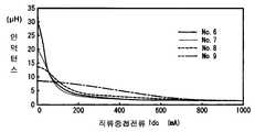
코일 패턴 담지층의 수를 10층으로 하고, 모든 층에 두께 5㎛의 자기 갭층을 형성한 점 외에는 시료 No.4와 마찬가지로 하여, 세로 3.2mm, 가로 1.6mm, 두께 1.0mm의 적층 부품(시료 No.11)을 제작하였다. 또한, 코일 패턴 담지층의 수를 12층으로 한 점 외에는 시료 No.11과 마찬가지로 하여 적층 부품(시료 No.12)을 제작하였다. 시료 No.11 및 시료 No.12는 모두, 소결 후의 자성체 기판층의 두께는 40㎛, 코일 패턴의 두께는 20㎛이며, 2턴의 권취수였다. 적층 부품의 직류 중첩 특성 및 DC-DC 변환 효율을 측정하였다. 결과를 표 5 및 도 45에 나타낸다.A laminated component having a length of 3.2 mm, a width of 1.6 mm, and a thickness of 1.0 mm in the same manner as in Sample No. 4, except that the number of coil pattern supporting layers was 10, and a magnetic gap layer having a thickness of 5 µm was formed on all layers. No. 11) was produced. A laminated component (sample No. 12) was produced in the same manner as in sample No. 11 except that the number of coil pattern carrying layers was 12. As for sample No. 11 and sample No. 12, the thickness of the magnetic substrate layer after sintering was 40 micrometers, the thickness of the coil pattern was 20 micrometers, and it was the number of turns of 2 turns. DC superposition characteristics and DC-DC conversion efficiency of the laminated component were measured. The results are shown in Table 5 and FIG. 45.
[표 5][Table 5]

표 5(계속)Table 5 (continued)

코일 패턴 담지층의 개수가 증가함에 따라 전류 무부하 시의 인덕턴스값, DC-DC 변환 효율이 증가하였다. 또한, 인덕턴스값이 전류 무부하 시의 80%로 저하되는 전류값은 모두 큰 값을 나타낸다.As the number of coil pattern bearing layers increased, the inductance value and DC-DC conversion efficiency at no current load increased. In addition, all the electric current values whose inductance value falls to 80% of no-load currents show large values.
[실시예 7][Example 7]
시료sampleNoNo.13∼.13 toNoNo.15의 제작(도 20 및 도 21에 나타낸 제5 적층 부품)Fabrication of .15 (fifth laminated part shown in FIGS. 20 and 21)
코일 패턴 담지층의 수를 12층으로 하고, 모든 층에 두께 10㎛의 자기 갭층을 형성한 점 외에는 시료 No.4와 마찬가지로 하여, 세로 3.2mm, 가로 1.6mm 및 두께 1.0mm의 적층 인덕터(시료 No.13)를 제작하였다. 또한, 모든 층에 두께 15㎛의 자기 갭층을 형성한 점 외에는 시료 No.13과 마찬가지로 하여 적층 인덕터(시료 No.14)를 제작하였다. 또한, 모든 층에 두께 20㎛의 자기 갭층을 형성한 점 외에는 시료 No.13과 마찬가지로 하여 적층 인덕터(시료 No.15)를 제작하였다. 시료 No.13∼No.15의 적층 인덕터는 모두, 소결 후의 자성체 기판층의 두께는 40㎛, 코일 패턴의 두께는 20㎛이며, 2턴의 권취수였다. 시료 No.13∼No.15의 적층 부품의 직류 중첩 특성 및 DC-DC 변환 효율을 측정하였다. 결과를 표 6 및 도 46에 나타낸다.A multilayer inductor having a length of 3.2 mm, a width of 1.6 mm, and a thickness of 1.0 mm (samples) was prepared in the same manner as in sample No. 4 except that the number of coil pattern carrying layers was 12, and a magnetic gap layer having a thickness of 10 µm was formed on all layers. No. 13) was produced. A multilayer inductor (sample No. 14) was produced in the same manner as in sample No. 13 except that a magnetic gap layer having a thickness of 15 μm was formed on all layers. A multilayer inductor (sample No. 15) was produced in the same manner as in sample No. 13 except that a magnetic gap layer having a thickness of 20 µm was formed on all layers. In the multilayer inductors of Samples Nos. 13 to 15, the thickness of the magnetic substrate layer after sintering was 40 µm and the thickness of the coil pattern was 20 µm, which was the number of turns of 2 turns. The direct current superimposition characteristic and DC-DC conversion efficiency of the laminated components of samples No.13-No.15 were measured. The results are shown in Table 6 and FIG. 46.
[표 6]TABLE 6

표 6(계속)Table 6 (continued)

자기 갭층이 두꺼워짐에 따라 전류 무부하 시의 인덕턴스값은 감소했지만, 전류 무부하 시의 80%로 저하되는 전류값은 대폭 향상되었다. 자기 갭층의 두께가 코일 패턴과 같은 20㎛인 적층 부품(시료 No.15)은, 다른 적층 부품과 비교하여 변환 효율이 낮았다. 이것은 자기 갭층의 자기 저항이 커지고, 코일 패턴 측으로 누출되는 자속이 증가하고, 와전류 손실의 증가에 의해 변환 효율이 감소했기 때문으로 여겨진다.As the magnetic gap layer became thicker, the inductance value at no current load decreased, but the current value lowered to 80% at no current load was greatly improved. The laminated component (Sample No. 15) whose thickness of the magnetic gap layer was 20 µm, which is the same as that of the coil pattern, was lower in conversion efficiency than other laminated components. This is considered to be because the magnetic resistance of the magnetic gap layer is increased, the magnetic flux leaking to the coil pattern side is increased, and the conversion efficiency is decreased by the increase of the eddy current loss.
이상 본 발명의 적층 부품을 설명하였으나, 코일 패턴 담지층의 개수, 1층 당 코일 패턴의 턴수, 코일 패턴 및 자기 갭층의 두께 및 재질 등은 실시예에 한정되지 않는다. 이들 파라미터를 적절하게 조정하여, 사용하는 전자 기기의 용도에 따른 원하는 자기 특성을 가지는 적층 부품을 제공할 수 있다.Although the laminated component of the present invention has been described above, the number of coil pattern carrying layers, the number of turns of the coil pattern per layer, the thickness and the material of the coil pattern and the magnetic gap layer are not limited to the examples. These parameters can be adjusted appropriately, and the laminated component which has desired magnetic characteristic according to the use of the electronic device to be used can be provided.
본 발명에 따른 적층 부품을 가지는 DC-DC 컨버터는, 전지를 사용하는 휴대형의 각종의 전자 기기(휴대 전화기, 휴대 정보 단말기 PDA, 노트북형 퍼스널 컴퓨터, 휴대형 음악/비디오 플레이어, 디지털 카메라, 디지털 비디오 카메라 등)에 유용하게 사용될 수 있다.The DC-DC converter having the laminated component according to the present invention is a portable electronic device using a battery (mobile phone, portable information terminal PDA, notebook personal computer, portable music / video player, digital camera, digital video camera). And the like).
Claims (14)
Translated fromKoreanApplications Claiming Priority (5)
| Application Number | Priority Date | Filing Date | Title |
|---|---|---|---|
| JP2006023775 | 2006-01-31 | ||
| JPJP-P-2006-00023775 | 2006-01-31 | ||
| JPJP-P-2006-00152542 | 2006-05-31 | ||
| JP2006152542 | 2006-05-31 | ||
| PCT/JP2007/051648WO2007088914A1 (en) | 2006-01-31 | 2007-01-31 | Laminated component and module using same |
Publications (2)
| Publication Number | Publication Date |
|---|---|
| KR20080091778A KR20080091778A (en) | 2008-10-14 |
| KR101372963B1true KR101372963B1 (en) | 2014-03-11 |
Family
ID=38327485
Family Applications (1)
| Application Number | Title | Priority Date | Filing Date |
|---|---|---|---|
| KR1020087018098AActiveKR101372963B1 (en) | 2006-01-31 | 2007-01-31 | Laminated component and module using same |
Country Status (6)
| Country | Link |
|---|---|
| US (2) | US7907044B2 (en) |
| EP (1) | EP1983531B1 (en) |
| JP (1) | JP4509186B2 (en) |
| KR (1) | KR101372963B1 (en) |
| CN (1) | CN101390176B (en) |
| WO (1) | WO2007088914A1 (en) |
Families Citing this family (111)
| Publication number | Priority date | Publication date | Assignee | Title |
|---|---|---|---|---|
| EP1609206B1 (en) | 2003-03-04 | 2010-07-28 | Rohm and Haas Electronic Materials, L.L.C. | Coaxial waveguide microstructures and methods of formation thereof |
| US7994889B2 (en)* | 2006-06-01 | 2011-08-09 | Taiyo Yuden Co., Ltd. | Multilayer inductor |
| EP2040272A4 (en) | 2006-07-05 | 2017-04-19 | Hitachi Metals, Ltd. | Laminated component |
| JP2008130736A (en)* | 2006-11-20 | 2008-06-05 | Hitachi Metals Ltd | Electronic component and its manufacturing method |
| US7656256B2 (en) | 2006-12-30 | 2010-02-02 | Nuvotronics, PLLC | Three-dimensional microstructures having an embedded support member with an aperture therein and method of formation thereof |
| KR101472134B1 (en) | 2007-03-20 | 2014-12-15 | 누보트로닉스, 엘.엘.씨 | Coaxial transmission line microstructure and method of forming the same |
| US7755174B2 (en) | 2007-03-20 | 2010-07-13 | Nuvotonics, LLC | Integrated electronic components and methods of formation thereof |
| JP4973996B2 (en)* | 2007-08-10 | 2012-07-11 | 日立金属株式会社 | Laminated electronic components |
| JP2009094149A (en)* | 2007-10-04 | 2009-04-30 | Hitachi Metals Ltd | Multilayered inductor |
| JP5262775B2 (en)* | 2008-03-18 | 2013-08-14 | 株式会社村田製作所 | Multilayer electronic component and manufacturing method thereof |
| JP5381983B2 (en)* | 2008-06-12 | 2014-01-08 | 株式会社村田製作所 | Electronic components |
| CN102067253B (en)* | 2008-08-07 | 2013-03-13 | 株式会社村田制作所 | Multilayer inductor |
| CN102232233A (en)* | 2008-12-03 | 2011-11-02 | 株式会社村田制作所 | Electronic component |
| JP2010147043A (en)* | 2008-12-16 | 2010-07-01 | Sony Corp | Inductor module and circuit module |
| WO2010084677A1 (en)* | 2009-01-22 | 2010-07-29 | 株式会社村田製作所 | Laminated inductor |
| JP5262813B2 (en)* | 2009-02-19 | 2013-08-14 | 株式会社村田製作所 | Electronic component and manufacturing method thereof |
| TWM365534U (en)* | 2009-05-08 | 2009-09-21 | Mag Layers Scient Technics Co | Improved laminated inductor sustainable to large current |
| JP5168234B2 (en)* | 2009-05-29 | 2013-03-21 | Tdk株式会社 | Multilayer type common mode filter |
| WO2010150602A1 (en)* | 2009-06-24 | 2010-12-29 | 株式会社村田製作所 | Electronic component and method for producing the same |
| US8193781B2 (en) | 2009-09-04 | 2012-06-05 | Apple Inc. | Harnessing power through electromagnetic induction utilizing printed coils |
| US20110123783A1 (en)* | 2009-11-23 | 2011-05-26 | David Sherrer | Multilayer build processses and devices thereof |
| US9330826B1 (en)* | 2010-02-12 | 2016-05-03 | The Board Of Trustees Of The University Of Alabama For And On Behalf Of The University Of Alabama | Integrated architecture for power converters |
| US8723634B2 (en) | 2010-04-30 | 2014-05-13 | Taiyo Yuden Co., Ltd. | Coil-type electronic component and its manufacturing method |
| JP4866971B2 (en) | 2010-04-30 | 2012-02-01 | 太陽誘電株式会社 | Coil-type electronic component and manufacturing method thereof |
| JP5402850B2 (en)* | 2010-06-21 | 2014-01-29 | 株式会社デンソー | Reactor |
| US8432049B2 (en)* | 2010-07-15 | 2013-04-30 | Sukho JUNG | Electrical generator |
| KR101414779B1 (en)* | 2010-10-20 | 2014-07-03 | 한국전자통신연구원 | Wireless power transfer device |
| JP6081051B2 (en) | 2011-01-20 | 2017-02-15 | 太陽誘電株式会社 | Coil parts |
| JP2012160506A (en)* | 2011-01-31 | 2012-08-23 | Toko Inc | Laminated type inductor |
| JP2012238840A (en) | 2011-04-27 | 2012-12-06 | Taiyo Yuden Co Ltd | Multilayer inductor |
| JP2012238841A (en) | 2011-04-27 | 2012-12-06 | Taiyo Yuden Co Ltd | Magnetic material and coil component |
| JP4906972B1 (en) | 2011-04-27 | 2012-03-28 | 太陽誘電株式会社 | Magnetic material and coil component using the same |
| US8866300B1 (en) | 2011-06-05 | 2014-10-21 | Nuvotronics, Llc | Devices and methods for solder flow control in three-dimensional microstructures |
| US8814601B1 (en) | 2011-06-06 | 2014-08-26 | Nuvotronics, Llc | Batch fabricated microconnectors |
| JP5991494B2 (en) | 2011-06-15 | 2016-09-14 | 株式会社村田製作所 | Multilayer coil parts |
| CN103608876B (en) | 2011-06-15 | 2017-08-15 | 株式会社村田制作所 | Laminated coil component and method of manufacturing the same |
| KR20130001984A (en)* | 2011-06-28 | 2013-01-07 | 삼성전기주식회사 | Gap composition of multi layered power inductor and multi layered power inductor comprising gap layer using the same |
| JP5032711B1 (en) | 2011-07-05 | 2012-09-26 | 太陽誘電株式会社 | Magnetic material and coil component using the same |
| WO2013010108A1 (en) | 2011-07-13 | 2013-01-17 | Nuvotronics, Llc | Methods of fabricating electronic and mechanical structures |
| JP5048155B1 (en)* | 2011-08-05 | 2012-10-17 | 太陽誘電株式会社 | Multilayer inductor |
| JP5881992B2 (en)* | 2011-08-09 | 2016-03-09 | 太陽誘電株式会社 | Multilayer inductor and manufacturing method thereof |
| JP5048156B1 (en) | 2011-08-10 | 2012-10-17 | 太陽誘電株式会社 | Multilayer inductor |
| KR101853129B1 (en)* | 2011-08-16 | 2018-06-07 | 삼성전기주식회사 | Multilayer power inductor |
| JP5082002B1 (en) | 2011-08-26 | 2012-11-28 | 太陽誘電株式会社 | Magnetic materials and coil parts |
| TWI436376B (en)* | 2011-09-23 | 2014-05-01 | Inpaq Technology Co Ltd | Common mode filter with multi spiral layer structure and method of manufacturing the same |
| KR101228645B1 (en)* | 2011-10-12 | 2013-01-31 | 삼성전기주식회사 | Multilayered ceramic electronic component |
| JP5598452B2 (en) | 2011-10-14 | 2014-10-01 | 株式会社村田製作所 | Electronic component and manufacturing method thereof |
| KR101853135B1 (en)* | 2011-10-27 | 2018-05-02 | 삼성전기주식회사 | Multilayer power inductor and method of manufacturing the same |
| JP6091744B2 (en) | 2011-10-28 | 2017-03-08 | 太陽誘電株式会社 | Coil type electronic components |
| JP6060368B2 (en)* | 2011-11-11 | 2017-01-18 | パナソニックIpマネジメント株式会社 | Multilayer inductor |
| JP5960971B2 (en) | 2011-11-17 | 2016-08-02 | 太陽誘電株式会社 | Multilayer inductor |
| JP6012960B2 (en) | 2011-12-15 | 2016-10-25 | 太陽誘電株式会社 | Coil type electronic components |
| KR20130077177A (en)* | 2011-12-29 | 2013-07-09 | 삼성전기주식회사 | Power inductor and manufacturing method for the same |
| US20130271251A1 (en)* | 2012-04-12 | 2013-10-17 | Cyntec Co., Ltd. | Substrate-Less Electronic Component |
| CN102637505A (en)* | 2012-05-02 | 2012-08-15 | 深圳顺络电子股份有限公司 | Laminated inductor with high self-resonant frequency and high quality factor |
| CN102709462A (en)* | 2012-05-02 | 2012-10-03 | 深圳顺络电子股份有限公司 | Laminated magnetic bead with large high-frequency impedance |
| KR101367952B1 (en)* | 2012-05-30 | 2014-02-28 | 삼성전기주식회사 | Non magnetic material for multi-layered electronic component, multi-layered electronic component manufactured by using the same and a process thereof |
| KR101792273B1 (en)* | 2012-06-14 | 2017-11-01 | 삼성전기주식회사 | Multi-layered chip electronic component |
| KR101872529B1 (en)* | 2012-06-14 | 2018-08-02 | 삼성전기주식회사 | Multi-layered chip electronic component |
| JP6097921B2 (en)* | 2012-07-13 | 2017-03-22 | パナソニックIpマネジメント株式会社 | Multilayer inductor |
| KR101771731B1 (en)* | 2012-08-28 | 2017-08-25 | 삼성전기주식회사 | Multi-layered chip electronic component |
| JP5816145B2 (en)* | 2012-09-06 | 2015-11-18 | 東光株式会社 | Multilayer inductor |
| JP5815640B2 (en)* | 2012-12-11 | 2015-11-17 | サムソン エレクトロ−メカニックス カンパニーリミテッド. | Manufacturing method of electronic components. |
| KR20140081355A (en)* | 2012-12-21 | 2014-07-01 | 삼성전기주식회사 | Electromagnetic induction module for wireless charging element and manufacturing method of the same |
| KR20140081356A (en)* | 2012-12-21 | 2014-07-01 | 삼성전기주식회사 | Electromagnetic induction module for wireless charging element and manufacturing method of the same |
| US9325044B2 (en) | 2013-01-26 | 2016-04-26 | Nuvotronics, Inc. | Multi-layer digital elliptic filter and method |
| JP5807650B2 (en)* | 2013-03-01 | 2015-11-10 | 株式会社村田製作所 | Multilayer coil and manufacturing method thereof |
| JP2014175349A (en)* | 2013-03-06 | 2014-09-22 | Murata Mfg Co Ltd | Laminated inductor |
| US9306255B1 (en) | 2013-03-15 | 2016-04-05 | Nuvotronics, Inc. | Microstructure including microstructural waveguide elements and/or IC chips that are mechanically interconnected to each other |
| US9306254B1 (en) | 2013-03-15 | 2016-04-05 | Nuvotronics, Inc. | Substrate-free mechanical interconnection of electronic sub-systems using a spring configuration |
| WO2014139169A1 (en)* | 2013-03-15 | 2014-09-18 | Laird Technologies, Inc. | Laminated high bias retention ferrite suppressors and methods of making the same |
| JP2015005632A (en)* | 2013-06-21 | 2015-01-08 | 株式会社村田製作所 | Method for manufacturing multilayer coil |
| JP6413209B2 (en)* | 2013-08-08 | 2018-10-31 | Tdk株式会社 | Multilayer coil parts |
| US20150102891A1 (en)* | 2013-10-16 | 2015-04-16 | Samsung Electro-Mechanics Co., Ltd. | Chip electronic component, board having the same, and packaging unit thereof |
| US10310009B2 (en) | 2014-01-17 | 2019-06-04 | Nuvotronics, Inc | Wafer scale test interface unit and contactors |
| KR101762778B1 (en) | 2014-03-04 | 2017-07-28 | 엘지이노텍 주식회사 | Wireless communication and charge substrate and wireless communication and charge device |
| KR101994734B1 (en)* | 2014-04-02 | 2019-07-01 | 삼성전기주식회사 | Multilayered electronic component and manufacturing method thereof |
| JP6381432B2 (en) | 2014-05-22 | 2018-08-29 | 新光電気工業株式会社 | Inductor, coil substrate, and method of manufacturing coil substrate |
| US10847469B2 (en) | 2016-04-26 | 2020-11-24 | Cubic Corporation | CTE compensation for wafer-level and chip-scale packages and assemblies |
| EP3224899A4 (en) | 2014-12-03 | 2018-08-22 | Nuvotronics, Inc. | Systems and methods for manufacturing stacked circuits and transmission lines |
| KR20160092394A (en)* | 2015-01-27 | 2016-08-04 | 삼성전기주식회사 | Inductor and manufacturing method thereof |
| DE102015206173A1 (en) | 2015-04-07 | 2016-10-13 | Würth Elektronik eiSos Gmbh & Co. KG | Electronic component and method for manufacturing an electronic component |
| US10825598B2 (en)* | 2015-05-13 | 2020-11-03 | Semiconductor Components Industries, Llc | Planar magnetic element |
| US10395810B2 (en)* | 2015-05-19 | 2019-08-27 | Shinko Electric Industries Co., Ltd. | Inductor |
| TWI592955B (en)* | 2015-06-25 | 2017-07-21 | Wafer Mems Co Ltd | Embedded passive components and methods of mass production |
| JP6575198B2 (en)* | 2015-07-24 | 2019-09-18 | Tdk株式会社 | Multilayer coil parts |
| JP6520604B2 (en)* | 2015-09-18 | 2019-05-29 | Tdk株式会社 | Laminated coil parts |
| KR101762027B1 (en)* | 2015-11-20 | 2017-07-26 | 삼성전기주식회사 | Coil component and manufacturing method for the same |
| JP6687881B2 (en)* | 2015-12-02 | 2020-04-28 | Tdk株式会社 | Coil device |
| WO2017124200A2 (en)* | 2016-01-20 | 2017-07-27 | Jaquet Technology Group Ag | Manufacturing method for a sensing element and sensor device |
| JP2017168472A (en)* | 2016-03-14 | 2017-09-21 | 株式会社村田製作所 | Multilayer board |
| JP6520880B2 (en)* | 2016-09-26 | 2019-05-29 | 株式会社村田製作所 | Electronic parts |
| JP6830347B2 (en)* | 2016-12-09 | 2021-02-17 | 太陽誘電株式会社 | Coil parts |
| JP6429951B2 (en)* | 2016-12-28 | 2018-11-28 | サムソン エレクトロ−メカニックス カンパニーリミテッド. | Coil component and manufacturing method thereof |
| JP6873263B2 (en)* | 2017-10-30 | 2021-05-19 | 三菱電機株式会社 | Power receiving device and non-contact power transmission system |
| US10319654B1 (en) | 2017-12-01 | 2019-06-11 | Cubic Corporation | Integrated chip scale packages |
| KR102511872B1 (en)* | 2017-12-27 | 2023-03-20 | 삼성전기주식회사 | Coil Electronic Component |
| JP7553220B2 (en)* | 2018-03-20 | 2024-09-18 | 太陽誘電株式会社 | Coil parts and electronic devices |
| JP7109232B2 (en)* | 2018-03-30 | 2022-07-29 | 戸田工業株式会社 | Module board antenna and module board using the same |
| CN108695040B (en)* | 2018-08-13 | 2021-10-08 | 西南应用磁学研究所 | A kind of LTCF device with air cavity and its manufacturing method |
| CN112236928B (en)* | 2018-08-17 | 2024-08-09 | 株式会社村田制作所 | Switching power supply device |
| JP7099178B2 (en)* | 2018-08-27 | 2022-07-12 | Tdk株式会社 | Multilayer coil parts |
| JP6981389B2 (en)* | 2018-10-05 | 2021-12-15 | 株式会社村田製作所 | Stacked coil array for DC-DC converter and DC-DC converter |
| JP7222217B2 (en)* | 2018-10-30 | 2023-02-15 | Tdk株式会社 | Laminated coil parts |
| JP2021027269A (en)* | 2019-08-08 | 2021-02-22 | 株式会社村田製作所 | Inductor |
| WO2021112086A1 (en)* | 2019-12-03 | 2021-06-10 | 戸田工業株式会社 | Module substrate antenna and module substrate using same |
| JP7234972B2 (en)* | 2020-02-25 | 2023-03-08 | 株式会社村田製作所 | coil parts |
| JP7579065B2 (en)* | 2020-03-31 | 2024-11-07 | 太陽誘電株式会社 | Coil parts |
| JP7428098B2 (en)* | 2020-07-31 | 2024-02-06 | Tdk株式会社 | Inductor parts and DC/DC converters using the same |
| JP7222383B2 (en)* | 2020-08-26 | 2023-02-15 | 株式会社村田製作所 | DC/DC converter parts |
| CN116825516A (en)* | 2022-03-21 | 2023-09-29 | 斯特华(佛山)磁材有限公司 | Multilayer inductor structure |
Citations (2)
| Publication number | Priority date | Publication date | Assignee | Title |
|---|---|---|---|---|
| KR20040047452A (en)* | 2002-11-30 | 2004-06-05 | 주식회사 쎄라텍 | Chip type power inductor and fabrication method thereof |
| JP2005045108A (en) | 2003-07-24 | 2005-02-17 | Fdk Corp | Magnetic core type multilayer inductor |
Family Cites Families (30)
| Publication number | Priority date | Publication date | Assignee | Title |
|---|---|---|---|---|
| JPS56155516A (en) | 1980-05-06 | 1981-12-01 | Tdk Corp | Laminated coil of open magnetic circuit type |
| US5206620A (en)* | 1987-07-01 | 1993-04-27 | Tdk Corporation | Sintered ferrite body, chip inductor, and composite LC part |
| JPH02165607A (en) | 1988-12-20 | 1990-06-26 | Toko Inc | laminated inductor |
| JPH06224043A (en)* | 1993-01-27 | 1994-08-12 | Taiyo Yuden Co Ltd | Laminated chip transformer and manufacture thereof |
| US5469399A (en) | 1993-03-16 | 1995-11-21 | Kabushiki Kaisha Toshiba | Semiconductor memory, memory card, and method of driving power supply for EEPROM |
| JPH0721791A (en)* | 1993-03-16 | 1995-01-24 | Toshiba Corp | Power supply driving method for semiconductor memory, memory card, and EEPROM |
| US5572487A (en)* | 1995-01-24 | 1996-11-05 | The United States Of America As Represented By The Secretary Of The Navy | High pressure, high frequency reciprocal transducer |
| US6566731B2 (en)* | 1999-02-26 | 2003-05-20 | Micron Technology, Inc. | Open pattern inductor |
| JP3582454B2 (en)* | 1999-07-05 | 2004-10-27 | 株式会社村田製作所 | Multilayer coil component and method of manufacturing the same |
| JP3621300B2 (en)* | 1999-08-03 | 2005-02-16 | 太陽誘電株式会社 | Multilayer inductor for power circuit |
| JP2001044037A (en)* | 1999-08-03 | 2001-02-16 | Taiyo Yuden Co Ltd | Laminated inductor |
| WO2002037709A1 (en)* | 2000-11-01 | 2002-05-10 | Hitachi Metals, Ltd. | High-frequency switch module |
| JP3791406B2 (en)* | 2001-01-19 | 2006-06-28 | 株式会社村田製作所 | Multilayer impedance element |
| JP2003158467A (en)* | 2001-08-27 | 2003-05-30 | Matsushita Electric Ind Co Ltd | RF device and communication device using the same |
| US6985712B2 (en) | 2001-08-27 | 2006-01-10 | Matsushita Electric Industrial Co., Ltd. | RF device and communication apparatus using the same |
| JP3767437B2 (en)* | 2001-09-05 | 2006-04-19 | 株式会社村田製作所 | Multilayer type common mode choke coil |
| JP2003347124A (en) | 2002-05-27 | 2003-12-05 | Matsushita Electric Ind Co Ltd | Magnetic element and power module using the same |
| JP2004343084A (en)* | 2003-04-21 | 2004-12-02 | Murata Mfg Co Ltd | Electronic component |
| JP2005053759A (en) | 2003-08-07 | 2005-03-03 | Koa Corp | Ferrite sintered compact and multilayer ferrite component using the same |
| AU2003266683A1 (en) | 2003-09-29 | 2005-04-14 | Tamura Corporation | Multilayer laminated circuit board |
| JP2005150168A (en) | 2003-11-11 | 2005-06-09 | Murata Mfg Co Ltd | Laminated coil component |
| JP2005268455A (en)* | 2004-03-17 | 2005-09-29 | Murata Mfg Co Ltd | Laminated electronic part |
| CN100546438C (en)* | 2004-03-31 | 2009-09-30 | 大见忠弘 | Circuit substrate and manufacture method thereof |
| US7304557B2 (en)* | 2004-06-07 | 2007-12-04 | Murata Manufacturing Co., Ltd. | Laminated coil |
| EP1710814B1 (en)* | 2005-01-07 | 2008-05-14 | Murata Manufacturing Co., Ltd. | Laminated coil |
| JP4725120B2 (en)* | 2005-02-07 | 2011-07-13 | 日立金属株式会社 | Multilayer inductor and multilayer substrate |
| US7262681B2 (en)* | 2005-02-11 | 2007-08-28 | Semiconductor Components Industries, L.L.C. | Integrated semiconductor inductor and method therefor |
| JP4213679B2 (en)* | 2005-03-18 | 2009-01-21 | Tdk株式会社 | Multilayer inductor |
| CN101341646B (en)* | 2005-10-28 | 2011-06-08 | 日立金属株式会社 | Dc-dc converter |
| US7932800B2 (en)* | 2006-02-21 | 2011-04-26 | Virginia Tech Intellectual Properties, Inc. | Method and apparatus for three-dimensional integration of embedded power module |
- 2007
- 2007-01-31CNCN2007800039461Apatent/CN101390176B/enactiveActive
- 2007-01-31EPEP07707834.3Apatent/EP1983531B1/enactiveActive
- 2007-01-31JPJP2007530526Apatent/JP4509186B2/enactiveActive
- 2007-01-31KRKR1020087018098Apatent/KR101372963B1/enactiveActive
- 2007-01-31USUS12/162,724patent/US7907044B2/enactiveActive
- 2007-01-31WOPCT/JP2007/051648patent/WO2007088914A1/enactiveApplication Filing
- 2011
- 2011-02-10USUS13/024,533patent/US8018313B2/enactiveActive
Patent Citations (2)
| Publication number | Priority date | Publication date | Assignee | Title |
|---|---|---|---|---|
| KR20040047452A (en)* | 2002-11-30 | 2004-06-05 | 주식회사 쎄라텍 | Chip type power inductor and fabrication method thereof |
| JP2005045108A (en) | 2003-07-24 | 2005-02-17 | Fdk Corp | Magnetic core type multilayer inductor |
Also Published As
| Publication number | Publication date |
|---|---|
| US7907044B2 (en) | 2011-03-15 |
| EP1983531B1 (en) | 2017-10-25 |
| JPWO2007088914A1 (en) | 2009-06-25 |
| JP4509186B2 (en) | 2010-07-21 |
| WO2007088914A1 (en) | 2007-08-09 |
| EP1983531A1 (en) | 2008-10-22 |
| KR20080091778A (en) | 2008-10-14 |
| CN101390176A (en) | 2009-03-18 |
| US8018313B2 (en) | 2011-09-13 |
| US20110128109A1 (en) | 2011-06-02 |
| EP1983531A4 (en) | 2014-07-02 |
| CN101390176B (en) | 2012-06-13 |
| US20090051476A1 (en) | 2009-02-26 |
Similar Documents
| Publication | Publication Date | Title |
|---|---|---|
| KR101372963B1 (en) | Laminated component and module using same | |
| JP4973996B2 (en) | Laminated electronic components | |
| CN101889319B (en) | Multilayer inductor and power conversion device using same | |
| KR101421455B1 (en) | Low-loss ferrite, and electronic component using the same | |
| JP2008130736A (en) | Electronic component and its manufacturing method | |
| JP5446262B2 (en) | Laminated parts | |
| US7646610B2 (en) | DC-DC converter | |
| JP2009094149A (en) | Multilayered inductor | |
| CN105305996B (en) | Combined electronical assembly and plate with the combined electronical assembly | |
| US9349512B2 (en) | Multi-layered chip electronic component | |
| JP4883392B2 (en) | DC-DC converter | |
| JP5429649B2 (en) | Inductor built-in component and DC-DC converter using the same | |
| JP5858630B2 (en) | Inductor-embedded substrate and electric circuit comprising the substrate | |
| JP2002222712A (en) | LC composite element | |
| CN119724819A (en) | Laminated inductor and method for manufacturing the same | |
| JPH02232915A (en) | Chip type lc composite ceramic component |
Legal Events
| Date | Code | Title | Description |
|---|---|---|---|
| PA0105 | International application | Patent event date:20080723 Patent event code:PA01051R01D Comment text:International Patent Application | |
| PG1501 | Laying open of application | ||
| A201 | Request for examination | ||
| PA0201 | Request for examination | Patent event code:PA02012R01D Patent event date:20111122 Comment text:Request for Examination of Application | |
| E902 | Notification of reason for refusal | ||
| PE0902 | Notice of grounds for rejection | Comment text:Notification of reason for refusal Patent event date:20130128 Patent event code:PE09021S01D | |
| E90F | Notification of reason for final refusal | ||
| PE0902 | Notice of grounds for rejection | Comment text:Final Notice of Reason for Refusal Patent event date:20130926 Patent event code:PE09021S02D | |
| E701 | Decision to grant or registration of patent right | ||
| PE0701 | Decision of registration | Patent event code:PE07011S01D Comment text:Decision to Grant Registration Patent event date:20131223 | |
| GRNT | Written decision to grant | ||
| PR0701 | Registration of establishment | Comment text:Registration of Establishment Patent event date:20140305 Patent event code:PR07011E01D | |
| PR1002 | Payment of registration fee | Payment date:20140305 End annual number:3 Start annual number:1 | |
| PG1601 | Publication of registration | ||
| FPAY | Annual fee payment | Payment date:20170221 Year of fee payment:4 | |
| PR1001 | Payment of annual fee | Payment date:20170221 Start annual number:4 End annual number:4 | |
| FPAY | Annual fee payment | Payment date:20180220 Year of fee payment:5 | |
| PR1001 | Payment of annual fee | Payment date:20180220 Start annual number:5 End annual number:5 | |
| FPAY | Annual fee payment | Payment date:20190219 Year of fee payment:6 | |
| PR1001 | Payment of annual fee | Payment date:20190219 Start annual number:6 End annual number:6 | |
| FPAY | Annual fee payment | Payment date:20200219 Year of fee payment:7 | |
| PR1001 | Payment of annual fee | Payment date:20200219 Start annual number:7 End annual number:7 | |
| PR1001 | Payment of annual fee | Payment date:20220222 Start annual number:9 End annual number:9 | |
| PR1001 | Payment of annual fee | Payment date:20230222 Start annual number:10 End annual number:10 | |
| PR1001 | Payment of annual fee | Payment date:20240220 Start annual number:11 End annual number:11 | |
| PR1001 | Payment of annual fee | Payment date:20250204 Start annual number:12 End annual number:12 |