KR101367916B1 - Self light emission display device, peak luminance control device, electronic apparatus, peak luminance control method and program - Google Patents
Self light emission display device, peak luminance control device, electronic apparatus, peak luminance control method and programDownload PDFInfo
- Publication number
- KR101367916B1 KR101367916B1KR1020060116312AKR20060116312AKR101367916B1KR 101367916 B1KR101367916 B1KR 101367916B1KR 1020060116312 AKR1020060116312 AKR 1020060116312AKR 20060116312 AKR20060116312 AKR 20060116312AKR 101367916 B1KR101367916 B1KR 101367916B1
- Authority
- KR
- South Korea
- Prior art keywords
- peak luminance
- gradation value
- power consumption
- average gradation
- period
- Prior art date
- Legal status (The legal status is an assumption and is not a legal conclusion. Google has not performed a legal analysis and makes no representation as to the accuracy of the status listed.)
- Active
Links
Images


Classifications
- G—PHYSICS
- G09—EDUCATION; CRYPTOGRAPHY; DISPLAY; ADVERTISING; SEALS
- G09G—ARRANGEMENTS OR CIRCUITS FOR CONTROL OF INDICATING DEVICES USING STATIC MEANS TO PRESENT VARIABLE INFORMATION
- G09G3/00—Control arrangements or circuits, of interest only in connection with visual indicators other than cathode-ray tubes
- G09G3/20—Control arrangements or circuits, of interest only in connection with visual indicators other than cathode-ray tubes for presentation of an assembly of a number of characters, e.g. a page, by composing the assembly by combination of individual elements arranged in a matrix no fixed position being assigned to or needed to be assigned to the individual characters or partial characters
- G09G3/22—Control arrangements or circuits, of interest only in connection with visual indicators other than cathode-ray tubes for presentation of an assembly of a number of characters, e.g. a page, by composing the assembly by combination of individual elements arranged in a matrix no fixed position being assigned to or needed to be assigned to the individual characters or partial characters using controlled light sources
- G09G3/30—Control arrangements or circuits, of interest only in connection with visual indicators other than cathode-ray tubes for presentation of an assembly of a number of characters, e.g. a page, by composing the assembly by combination of individual elements arranged in a matrix no fixed position being assigned to or needed to be assigned to the individual characters or partial characters using controlled light sources using electroluminescent panels
- G09G3/32—Control arrangements or circuits, of interest only in connection with visual indicators other than cathode-ray tubes for presentation of an assembly of a number of characters, e.g. a page, by composing the assembly by combination of individual elements arranged in a matrix no fixed position being assigned to or needed to be assigned to the individual characters or partial characters using controlled light sources using electroluminescent panels semiconductive, e.g. using light-emitting diodes [LED]
- G09G3/3208—Control arrangements or circuits, of interest only in connection with visual indicators other than cathode-ray tubes for presentation of an assembly of a number of characters, e.g. a page, by composing the assembly by combination of individual elements arranged in a matrix no fixed position being assigned to or needed to be assigned to the individual characters or partial characters using controlled light sources using electroluminescent panels semiconductive, e.g. using light-emitting diodes [LED] organic, e.g. using organic light-emitting diodes [OLED]
- G09G3/3225—Control arrangements or circuits, of interest only in connection with visual indicators other than cathode-ray tubes for presentation of an assembly of a number of characters, e.g. a page, by composing the assembly by combination of individual elements arranged in a matrix no fixed position being assigned to or needed to be assigned to the individual characters or partial characters using controlled light sources using electroluminescent panels semiconductive, e.g. using light-emitting diodes [LED] organic, e.g. using organic light-emitting diodes [OLED] using an active matrix
- G09G3/3233—Control arrangements or circuits, of interest only in connection with visual indicators other than cathode-ray tubes for presentation of an assembly of a number of characters, e.g. a page, by composing the assembly by combination of individual elements arranged in a matrix no fixed position being assigned to or needed to be assigned to the individual characters or partial characters using controlled light sources using electroluminescent panels semiconductive, e.g. using light-emitting diodes [LED] organic, e.g. using organic light-emitting diodes [OLED] using an active matrix with pixel circuitry controlling the current through the light-emitting element
- G—PHYSICS
- G09—EDUCATION; CRYPTOGRAPHY; DISPLAY; ADVERTISING; SEALS
- G09G—ARRANGEMENTS OR CIRCUITS FOR CONTROL OF INDICATING DEVICES USING STATIC MEANS TO PRESENT VARIABLE INFORMATION
- G09G3/00—Control arrangements or circuits, of interest only in connection with visual indicators other than cathode-ray tubes
- G09G3/20—Control arrangements or circuits, of interest only in connection with visual indicators other than cathode-ray tubes for presentation of an assembly of a number of characters, e.g. a page, by composing the assembly by combination of individual elements arranged in a matrix no fixed position being assigned to or needed to be assigned to the individual characters or partial characters
- G09G3/22—Control arrangements or circuits, of interest only in connection with visual indicators other than cathode-ray tubes for presentation of an assembly of a number of characters, e.g. a page, by composing the assembly by combination of individual elements arranged in a matrix no fixed position being assigned to or needed to be assigned to the individual characters or partial characters using controlled light sources
- G09G3/28—Control arrangements or circuits, of interest only in connection with visual indicators other than cathode-ray tubes for presentation of an assembly of a number of characters, e.g. a page, by composing the assembly by combination of individual elements arranged in a matrix no fixed position being assigned to or needed to be assigned to the individual characters or partial characters using controlled light sources using luminous gas-discharge panels, e.g. plasma panels
- G09G3/288—Control arrangements or circuits, of interest only in connection with visual indicators other than cathode-ray tubes for presentation of an assembly of a number of characters, e.g. a page, by composing the assembly by combination of individual elements arranged in a matrix no fixed position being assigned to or needed to be assigned to the individual characters or partial characters using controlled light sources using luminous gas-discharge panels, e.g. plasma panels using AC panels
- G09G3/291—Control arrangements or circuits, of interest only in connection with visual indicators other than cathode-ray tubes for presentation of an assembly of a number of characters, e.g. a page, by composing the assembly by combination of individual elements arranged in a matrix no fixed position being assigned to or needed to be assigned to the individual characters or partial characters using controlled light sources using luminous gas-discharge panels, e.g. plasma panels using AC panels controlling the gas discharge to control a cell condition, e.g. by means of specific pulse shapes
- G—PHYSICS
- G09—EDUCATION; CRYPTOGRAPHY; DISPLAY; ADVERTISING; SEALS
- G09G—ARRANGEMENTS OR CIRCUITS FOR CONTROL OF INDICATING DEVICES USING STATIC MEANS TO PRESENT VARIABLE INFORMATION
- G09G3/00—Control arrangements or circuits, of interest only in connection with visual indicators other than cathode-ray tubes
- G09G3/20—Control arrangements or circuits, of interest only in connection with visual indicators other than cathode-ray tubes for presentation of an assembly of a number of characters, e.g. a page, by composing the assembly by combination of individual elements arranged in a matrix no fixed position being assigned to or needed to be assigned to the individual characters or partial characters
- G09G3/22—Control arrangements or circuits, of interest only in connection with visual indicators other than cathode-ray tubes for presentation of an assembly of a number of characters, e.g. a page, by composing the assembly by combination of individual elements arranged in a matrix no fixed position being assigned to or needed to be assigned to the individual characters or partial characters using controlled light sources
- G09G3/30—Control arrangements or circuits, of interest only in connection with visual indicators other than cathode-ray tubes for presentation of an assembly of a number of characters, e.g. a page, by composing the assembly by combination of individual elements arranged in a matrix no fixed position being assigned to or needed to be assigned to the individual characters or partial characters using controlled light sources using electroluminescent panels
- G09G3/32—Control arrangements or circuits, of interest only in connection with visual indicators other than cathode-ray tubes for presentation of an assembly of a number of characters, e.g. a page, by composing the assembly by combination of individual elements arranged in a matrix no fixed position being assigned to or needed to be assigned to the individual characters or partial characters using controlled light sources using electroluminescent panels semiconductive, e.g. using light-emitting diodes [LED]
- G—PHYSICS
- G09—EDUCATION; CRYPTOGRAPHY; DISPLAY; ADVERTISING; SEALS
- G09G—ARRANGEMENTS OR CIRCUITS FOR CONTROL OF INDICATING DEVICES USING STATIC MEANS TO PRESENT VARIABLE INFORMATION
- G09G2300/00—Aspects of the constitution of display devices
- G09G2300/08—Active matrix structure, i.e. with use of active elements, inclusive of non-linear two terminal elements, in the pixels together with light emitting or modulating elements
- G09G2300/0809—Several active elements per pixel in active matrix panels
- G09G2300/0842—Several active elements per pixel in active matrix panels forming a memory circuit, e.g. a dynamic memory with one capacitor
- G09G2300/0861—Several active elements per pixel in active matrix panels forming a memory circuit, e.g. a dynamic memory with one capacitor with additional control of the display period without amending the charge stored in a pixel memory, e.g. by means of additional select electrodes
- G—PHYSICS
- G09—EDUCATION; CRYPTOGRAPHY; DISPLAY; ADVERTISING; SEALS
- G09G—ARRANGEMENTS OR CIRCUITS FOR CONTROL OF INDICATING DEVICES USING STATIC MEANS TO PRESENT VARIABLE INFORMATION
- G09G2330/00—Aspects of power supply; Aspects of display protection and defect management
- G09G2330/02—Details of power systems and of start or stop of display operation
- G09G2330/021—Power management, e.g. power saving
- G—PHYSICS
- G09—EDUCATION; CRYPTOGRAPHY; DISPLAY; ADVERTISING; SEALS
- G09G—ARRANGEMENTS OR CIRCUITS FOR CONTROL OF INDICATING DEVICES USING STATIC MEANS TO PRESENT VARIABLE INFORMATION
- G09G2330/00—Aspects of power supply; Aspects of display protection and defect management
- G09G2330/02—Details of power systems and of start or stop of display operation
- G09G2330/025—Reduction of instantaneous peaks of current
- G—PHYSICS
- G09—EDUCATION; CRYPTOGRAPHY; DISPLAY; ADVERTISING; SEALS
- G09G—ARRANGEMENTS OR CIRCUITS FOR CONTROL OF INDICATING DEVICES USING STATIC MEANS TO PRESENT VARIABLE INFORMATION
- G09G3/00—Control arrangements or circuits, of interest only in connection with visual indicators other than cathode-ray tubes
- G09G3/20—Control arrangements or circuits, of interest only in connection with visual indicators other than cathode-ray tubes for presentation of an assembly of a number of characters, e.g. a page, by composing the assembly by combination of individual elements arranged in a matrix no fixed position being assigned to or needed to be assigned to the individual characters or partial characters
- G09G3/2007—Display of intermediate tones
- G09G3/2014—Display of intermediate tones by modulation of the duration of a single pulse during which the logic level remains constant
Landscapes
- Engineering & Computer Science (AREA)
- Physics & Mathematics (AREA)
- Computer Hardware Design (AREA)
- General Physics & Mathematics (AREA)
- Theoretical Computer Science (AREA)
- Power Engineering (AREA)
- Plasma & Fusion (AREA)
- Control Of Indicators Other Than Cathode Ray Tubes (AREA)
- Electroluminescent Light Sources (AREA)
- Control Of El Displays (AREA)
- Transforming Electric Information Into Light Information (AREA)
Abstract
Translated fromKorean
Description
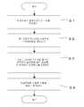
Translated fromKorean도 1은, 발광 시간과 발광 휘도의 관계를 설명하는 도면이다.1 is a diagram illustrating a relationship between light emission time and light emission luminance.
도 2는, 출력전압과 발광 휘도와의 관계를 설명하는 도면이다.2 is a diagram illustrating a relationship between an output voltage and light emission luminance.
도 3은, 유기 EL패널 모듈의 구조 예를 나타내는 도면이다.3 is a diagram illustrating a structural example of an organic EL panel module.
도 4는, 발광 시간길이를 제어하는 듀티 펄스 예를 나타내는 도면이다.4 is a diagram showing an example of a duty pulse for controlling the light emission time length.
도 5는, 유기 EL패널 모듈의 구조 예를 나타내는 도면이다.5 is a diagram illustrating a structural example of an organic EL panel module.
도 6은, 피크 휘도 조정 장치의 구성 예를 나타내는 도면이다.6 is a diagram illustrating an example of a configuration of a peak luminance adjusting device.
도 7은, 평균 계조치 산출부의 내부 구성 예를 나타내는 도면이다.7 is a diagram illustrating an internal configuration example of an average gradation value calculation unit.
도 8은, 소비 전력량 일정화 제어부의 내부 구성 예를 나타내는 도면이다.8 is a diagram illustrating an internal configuration example of a power consumption constant controller.
도 9는, 평균 계조치에 피크 휘도 배율을 대응시킨 룩업테이블 예를 나타내는 도면이다.9 is a diagram illustrating an example of a lookup table in which peak luminance magnification is associated with an average gradation value.
도 10은, 각 부의 위상 관계를 나타내는 도면이다.10 is a diagram illustrating the phase relationship between the units.
도 11은, 피크 휘도 조정 장치가 실행하는 처리 동작 예를 나타내는 도면이다.11 is a diagram illustrating an example of a processing operation executed by the peak luminance adjusting device.
도 12는, 피크 휘도 조정에 의한 소비 전력량의 추이 예를 나타내는 도면이 다.12 is a diagram illustrating a transition example of power consumption amount by adjusting peak luminance.
<도면의 주요부분에 대한 부호의 설명><Description of the symbols for the main parts of the drawings>
1 : 유기 EL패널 모듈 3A : 발광 영역1: organic EL panel module 3A: light emitting area
5 : 데이터 드라이버 7A : 전압 전환 드라이버5:
7B : 게이트 스캔 드라이버7B: Gate Scan Driver
7C : 점등 시간 제어용 게이트 드라이버7C: Gate driver for lighting time control
9 : 타이밍 제너레이터 11 : 피크 휘도 조정 장치9: timing generator 11: peak luminance adjustment device
13 : 평균 계조치 산출부 15 : 소비 전력량 일정화 제어부13: Average gradation value calculation part 15: Power consumption constant control part
17 : 피크 휘도 제어부 19 : 프레임 지연부17 peak
151 : 소비 전력 산출부 153 : 피크 휘도 조정부151 power consumption calculator 153 peak luminance adjustment unit
이 명세서로 설명하는 발명은, 자발광 표시 패널(장치)에서 소비되는 전력을 규정 범위내로 강제적으로 억제하는 기술에 관한 것이다.The invention described in this specification relates to a technique for forcibly suppressing power consumed in a self-luminous display panel (device) within a prescribed range.
또한, 발명자들이 제안하는 발명은, 자발광 표시장치, 피크 휘도 조정 장치, 전자기기, 피크 휘도 조정 방법 및 프로그램으로서의 측면을 가진다.In addition, the invention proposed by the inventors has aspects as a self-luminous display device, a peak brightness adjusting device, an electronic device, a peak brightness adjusting method and a program.
유기 EL디스플레이는, 광(廣)시야각 특성, 응답 속도, 광(廣)색재현성 범위, 고(高) 콘트라스트 성능이 뛰어날 뿐만 아니라, 표시 패널 자체를 얇게 형성할 수 있다. 이들의 이점에 의해, 유기 EL디스플레이는, 차세대 플랫 패널 디스플레이 의 최유력 후보로서 주목받고 있다.The organic EL display is excellent in light viewing angle characteristics, response speed, light color reproducibility range, high contrast performance, and can form a thin display panel itself. By these advantages, the organic EL display is attracting attention as a potential candidate for the next generation flat panel display.
더욱이 요즈음에는, 응답 속도나 콘트라스트 성능을 발광 시간의 가변 제어를 통하여 개선하는 수법이 검토되고 있다. 발광 시간의 가변 제어 기술을 개시하는 공지 기술에는, 예를 들면 이하에 나타내는 특허 문헌 1~3이 있다.In recent years, techniques for improving response speed and contrast performance through variable control of light emission time have been studied. As a well-known technique which discloses the variable control of light emission time, there exist patent documents 1-3 shown below, for example.
[특허 문헌 1]특개 2003-015605호 공보[Patent Document 1] Japanese Patent Application Laid-Open No. 2003-015605
[특허 문헌 2]특개 2001-343941호 공보[Patent Document 2] Japanese Patent Application Laid-Open No. 2001-343941
[특허 문헌 3]특개 2002-132218호 공보[Patent Document 3] Japanese Patent Application Laid-Open No. 2002-132218
그런데, 특허 문헌 1~3에 개시된 각 발명은, 모두 화질의 향상을 목적으로서 검토된 것이지만, 일정한 소비전력화나 소비전력의 억제화에 대한 시점(視點)은 검토되어 있지 않다.By the way, although each invention disclosed by patent documents 1-3 was examined for the purpose of the improvement of image quality, the viewpoint about the constant power consumption reduction and the suppression of power consumption is not examined.
실제, 유기 EL디스플레이 그 외의 자발광 표시장치에서는, 일정 휘도의 백라이트를 상시 점등 상태 시키는 방식의 표시장치와는 다르며, 입력되는 영상 신호에 따라 표시 패널에 흐르는 전류량이 극적으로 변화하는 특성이 있다.In fact, the organic EL display and other self-luminous display devices differ from the display devices in which a backlight having a constant luminance is always turned on, and has a characteristic that the amount of current flowing through the display panel varies dramatically depending on the input video signal.
이 특성 때문에, 자발광 표시장치에 있어서의 단위시간 당의 소비 전력은 일정하게는 되지 않는다. 즉, 표시 패널의 소비 전력이 표시 내용에 따라 극단적으로 변화하는 문제가 있다. 또, 표시 패널을 탑재하는 전자기기가 배터리 구동되는 경우에는, 표시 내용에 따라 사용시간이 극단적으로 변화하는 문제가 있다. 이 문제를 해결하는데에는, 배터리 용량을 대형화할 필요가 있다.Because of this characteristic, the power consumption per unit time in the self-luminous display device does not become constant. That is, there is a problem that the power consumption of the display panel changes extremely depending on the display contents. In addition, when the electronic device equipped with the display panel is battery driven, there is a problem that the use time is extremely changed depending on the display contents. In order to solve this problem, it is necessary to increase the battery capacity.
발명자들은, 자발광 패널면의 피크 휘도를 1 프레임 단위로 조정하는 피크 휘도 조정 장치로서, 이하의 각 기능을 탑재하는 것을 제안한다.The inventors propose to mount the following functions as a peak brightness adjusting device for adjusting the peak brightness of the surface of the self-luminous panel in units of one frame.
(a)1 프레임 기간 중에 입력되는 영상 신호의 평균 계조치(階調値)를 산출하는 평균 계조치 산출부(a) An average gradation value calculating unit that calculates an average gradation value of a video signal input during one frame period.
(b)산출된 평균 계조치에 따른 표준 피크 휘도를 구하며, 당해 표준 피크 휘도와 산출된 평균 계조치로 소비되는 소비 전력량을 산출하는 소비 전력 산출부(b) a power consumption calculation unit for calculating a standard peak luminance according to the calculated average gradation value and calculating the amount of power consumed by the standard peak luminance and the calculated average gradation value.
(c)일정기간내에 소비되는 소비 전력의 합계치가 설정 전력량을 넘지 않도록, 표준 피크 휘도를 조정하는 피크 휘도 조정부(c) Peak luminance adjustment unit for adjusting the standard peak luminance so that the total value of power consumption consumed within a predetermined period does not exceed the set amount of power.
이하, 발명에 관계되는 처리 기능을 탑재한 유기 EL패널 모듈에 대하여 설명한다.Hereinafter, the organic EL panel module equipped with the processing function which concerns on this invention is demonstrated.
또한, 본 명세서에서 특히 도시 또는 기재되지 않는 부분에는, 당해 기술 분야의 주지 또는 공지 기술을 적용한다.In addition, the well-known or well-known technique of the said technical field is applied to the part which is not shown or described especially in this specification.
또 이하에 설명하는 형태 예는, 발명의 하나의 형태 예이며, 이들로 한정되는 것은 아니다.Moreover, the form example described below is an example of one aspect of this invention, It is not limited to these.
(A)피크 휘도의 조정(A) Peak luminance adjustment
표시 패널의 피크 휘도는, 최대 데이터의 입력시에 표시 소자에 인가되는 출력전압(출력 전류) 또는 발광 시간의 가변 제어에 의해 조정할 수 있다.The peak luminance of the display panel can be adjusted by variable control of the output voltage (output current) or the light emission time applied to the display element at the time of maximum data input.
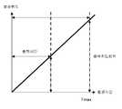
도 1에, 발광 시간과 발광 휘도와의 관계를 나타낸다. 도 1에 나타내는 바와 같이, 발광 휘도는 발광 시간에 대하여 선형으로 변화한다.1 shows the relationship between the light emission time and the light emission luminance. As shown in Fig. 1, the light emission luminance changes linearly with respect to the light emission time.
도 2a에, 표시 소자에 인가되는 출력전압과 발광 휘도와의 관계를 나타낸다. 도 2b에, 입력 영상 신호의 계조치(%)와 표시 소자에 인가되는 출력전압(기준치를 100%로 나타낸다.)과의 사이의 입출력 관계를 나타낸다.2A shows the relationship between the output voltage applied to the display element and the light emission luminance. 2B shows the input / output relationship between the gray scale value (%) of the input video signal and the output voltage (represented by 100%) applied to the display element.
여기에서, 도 2b에 실선으로 나타내는 곡선은 기준치에 대응하는 입출력 관계이며, 파선으로 나타내는 곡선은 최대 데이터의 입력시에 표시소자에 인가되는 최대 출력전압(Vmax)(최대 출력 전류(Imax))을 가변 제어했을 경우의 입출력 관계를 나타낸다. 도 2에 나타내는 바와 같이, 같은 입력 계조치에서도 최대 출력전압(Vmax)(최대 출력 전류(Imax))을 가변 제어하면, 발광 휘도가 가변 제어된다.Here, the curve shown by the solid line in FIG. 2B is an input / output relationship corresponding to the reference value, and the curve shown by the broken line indicates the maximum output voltage Vmax (maximum output current Imax ) applied to the display element at the time of maximum data input. ) Shows the I / O relationship when variable control is performed. As shown in FIG. 2, when the maximum output voltage Vmax (maximum output current Imax ) is variably controlled even at the same input gradation value, light emission luminance is variably controlled.
그런데, 표시 패널의 피크 휘도는, 최대 출력전압(Vmax)(최대 출력 전류(Imax))과 발광 시간과의 곱(S)으로 주어진다.By the way, the peak luminance of the display panel is given by the product S of the maximum output voltage Vmax (maximum output current Imax ) and the light emission time.
따라서 발광 시간 또는 최대 출력전압(Vmax)(최대 출력 전류(Imax))을 개별적으로 가변 제어하면, 표시 패널의 피크 휘도를 가변 제어하는 것이 가능해진다.Therefore, if the light emission time or the maximum output voltage Vmax (maximum output current Imax ) are individually controlled, the peak luminance of the display panel can be variably controlled.
(B)유기 EL패널의 구조 예(B) Structure example of organic EL panel
계속해서, 피크 휘도의 가변 제어를 가능하게 하는 유기 EL패널 모듈의 구조 예를 설명한다.Subsequently, an example of the structure of an organic EL panel module that enables variable control of peak luminance is described.
도 3에, 유기 EL패널 모듈(1)의 구조 예를 나타낸다. 유기 EL패널 모듈(1)은, 발광 영역(3A)(유기 EL소자가 매트릭스모양으로 배열된 영역)과 화상의 표시를 제어하는 패널 구동 회로로 구성된다.3 shows an example of the structure of the organic
패널 구동 회로는, 데이터 드라이버(5), 최대 출력전압 제어용 드라이 버(7A), 게이트 스캔 드라이버(7B), 점등 시간 제어용 게이트 드라이버(7C)로 구성된다. 또한, 패널 구동 회로는, 발광 영역(3A)의 주변부에 형성한다.The panel drive circuit is composed of a
각 화소에 대응하는 유기 EL소자(3B)와 그 구동 회로(화소 구동 회로)(3C)는, 데이터선(3D)과 주사선(3E)의 교점 위치에 배치되어 있다. 화소 구동 회로(3C)는, 데이터 스위치 소자(T1), 커패시터(C1), 전류 구동 소자(T2), 점등 스위치 소자(T3)로 구성된다.The
이 중, 데이터 스위치 소자(T1)는, 데이터선(3D)을 통하여 주어지는 전압치의 취득 타이밍(fetching timing)을 제어하는데 이용된다. 취득 타이밍은, 주사선(3E)을 통하여 선순차(line-sequential)로 주어진다.Among these, the data switch element T1 is used to control the fetching timing of the voltage value given through the data line 3D. The acquisition timing is given in line-sequential through the scanning line 3E.
커패시터(C1)는, 취득한 전압치를 1 프레임 기간 보관 유지하는데 이용된다. 커패시터(C1)를 이용함으로써, 면순차(plane-sequential) 구동이 실현된다.The capacitor C1 is used to hold the obtained voltage value for one frame period. By using the capacitor C1, plane-sequential driving is realized.
전류 구동 소자(T2)는, 커패시터(C1)의 전압치에 따른 전류를 유기 EL소자(3B)에 공급하는데 이용된다. 구동 전류는, 전류 공급선(3F)을 통하여 공급된다. 또한, 이 전류 공급선(3F)에는, 최대 출력전압 제어용 드라이버(7A)를 통하여 최대 출력전압(Vmax)이 인가된다.The current drive element T2 is used to supply a current corresponding to the voltage value of the capacitor C1 to the
점등 스위치 소자(T3)는, 유기 EL소자(3B)에 대한 구동 전류의 공급을 제어하는데 이용된다. 점등 스위치 소자(T3)는, 구동 전류의 공급 경로에 대하여 직렬로 배치된다. 점등 스위치 소자(T3)가 닫혀 있는 동안, 유기 EL소자(3B)가 점등한다. 한편, 점등 스위치 소자(T3)가 열려 있는 동안, 유기 EL소자(3B)가 소 등한다.The lighting switch element T3 is used to control the supply of the drive current to the
이 점등 스위치 소자(T3)의 개폐 동작을 제어하는 듀티 펄스(도4b)를 공급하는 것이 점등 제어선(3G)이다. 또한, 도 4a는, 기준 기간으로서의 1 프레임 기간을 나타낸다.The lighting control line 3G supplies the duty pulse (Fig. 4B) for controlling the opening and closing operation of the lighting switch element T3. 4A shows one frame period as a reference period.
여기에서, 전류 공급선(3F)에 인가하는 전압의 가변 제어는, 최대 출력전압 제어용 드라이버(7A)가 실행한다. 또, 발광 시간의 가변 제어는, 점등 시간 제어용 게이트 드라이버(7C)가 실행한다. 이들 드라이버의 제어 신호는, 후술하는 발광 조건 제어장치에서 공급된다.Here, the maximum output
또한, 피크 휘도를 발광 시간길이로 제어하는 경우에는, 최대 출력전압 제어용 드라이버(7A)는 모든 프레임에 대하여 고정 전압을 공급한다. 한편, 피크 휘도를 최대 출력전압(Vmax)으로 제어하는 경우에는, 점등 시간 제어용 게이트 드라이버(7C)는, 모든 프레임에 대하여 고정비(固定比)의 듀티 펄스를 공급한다.In addition, when controlling the peak luminance to the light emission time length, the maximum output
도 5에, 화소 구동 회로(3C)를 형성한 발광 영역(3A)을 탑재하는 유기 EL패널 모듈(1)의 구조 예를 나타낸다. 도 5의 경우, 피크 휘도 조정 장치(11)는, 타이밍 제너레이터(9)의 일부분으로서 실장한다.5, the structural example of the organic
또한, 발광 영역(3A)의 주변 회로(패널 구동 회로)는, 반도체 집적회로로서 패널 기판상에 탑재해도 좋으며, 패널 기판상에 반도체 프로세스를 이용하여 직접 형성해도 좋다.The peripheral circuit (panel drive circuit) of the light emitting region 3A may be mounted on a panel substrate as a semiconductor integrated circuit, or may be formed directly on the panel substrate using a semiconductor process.
(C)피크 휘도 조정 장치의 형태 예(C) Example of form of peak luminance adjusting device
이하, 일정기간내에 소비되는 소비 전력의 합계치가 설정 전력량을 넘지 않도록, 영상 신호의 피크 휘도를 실시간으로 제어 가능한 피크 휘도 조정 장치(11)(도 6)의 형태 예를 설명한다.Hereinafter, an example of the form of the peak luminance adjustment device 11 (FIG. 6) capable of controlling the peak luminance of the video signal in real time so that the total value of power consumption consumed within a certain period does not exceed the set amount of power.
(C-1)피크 휘도 조정 장치의 구성 예(C-1) Configuration example of peak luminance adjustment device
도 6에, 피크 휘도 조정 장치(11)에 채용하여 매우 적합한 구성 예의 하나를 나타낸다.6 shows one example of a configuration that is very suitable for use in the peak
이 형태 예에 관계되는 피크 휘도 조정 장치(11)는, 평균 계조치 산출부(13)와, 소비 전력량 일정화 제어부(15)와, 피크 휘도 제어부(17)와, 프레임 지연부(19)로 구성한다.The peak
평균 계조치 산출부(13)는, 1 프레임 기간중에 입력되는 영상 신호의 평균 계조치(APLn)를 프레임 단위로 산출하는 처리 디바이스이다. 여기에서의 첨자(n)는, 시간(예를 들면 프레임 번호)을 의미한다.The average gradation
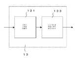
도 7에, 평균 계조치 산출부(13)의 내부 구성 예를 나타낸다. 평균 계조치 산출부(13)는, 그레이 스케일 변환부(131)와 1 프레임내 전화소 계조 평균 계산부(133)로 구성한다.7 shows an internal configuration example of the average gradation
그레이 스케일 변환부(131)는, 입력된 영상 신호를 그레이 스케일 신호로 변환하는 처리 디바이스이다.The gray scale converter 131 is a processing device for converting an input video signal into a gray scale signal.
1 프레임내 전화소 계조 평균 계산부(133)는, 1 프레임을 구성하는 전화소에 대하여 계조치의 평균치를 산출하는 처리 디바이스이다.The intraframe telephone tone gradation average calculation unit 133 is a processing device that calculates an average value of the gradation values for the telephone stations constituting one frame.
소비 전력량 일정화 제어부(15)는, 일정기간내에서의 소비 전력이 설정 전력량에 들어가도록, 각 프레임의 소비 전력량을 잔존하는 소비 전력량에 따라 조정하는 처리 디바이스이다.The power consumption
도 8에, 소비 전력량 일정화 제어부(15)의 내부 구성 예를 나타낸다. 소비 전력량 일정화 제어부(15)는, 소비 전력 산출부(151)와, 피크 휘도 조정부(153)로 구성한다.8 shows an example of the internal configuration of the power consumption
소비 전력 산출부(151)는, 산출된 평균 계조치(APL)에 따른 표준 피크 휘도를 독출(讀出)하고, 당해 표준 피크 휘도와 산출된 평균 계조치로 소비되는 소비 전력량을 산출하는 처리 디바이스이다.The power
이 형태 예의 경우, 표준 피크 휘도는, 피크 휘도 배율(SEL_PK)로 준다. 피크 휘도 배율(SEL_PK)은, 기준 피크 휘도에 대한 배율이며, 사전에 설정되는 것으로 한다.In the case of this example, the standard peak luminance is given by the peak luminance magnification SEL_PK. The peak luminance magnification SEL_PK is a magnification with respect to the reference peak luminance, and it is assumed to be set in advance.
이 경우, 어떤 프레임의 소비 전력은, 평균 계조치(APL)×피크 휘도 배율(SEL_PK)×기준 피크 휘도로 주어진다.In this case, the power consumption of a certain frame is given by the average gradation value APL x peak luminance magnification SEL_PK x reference peak luminance.
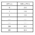
소비 전력 산출부(151)는, 평균 계조치(APL)에 따른 피크 휘도 배율(SEL_PK)을, 도 9에 나타내는 룩업테이블을 사용하여 읽어낸다.The power
도 9에 나타내는 룩업테이블에서는, 평균 계조치(APL)가 작을수록, 피크 휘도 배율(SEL_PK)을 큰 값으로 설정한다. 도 9에서는, 2배로 설정한다. 이것은 평균 계조치가 낮은 화면내에 고휘도 영역이 포함될 경우(예를 들면, 밤하늘의 영상에 별이 빛나는 경우)에도 충분한 콘트라스트를 확보하기 위해서이다.In the look-up table shown in Fig. 9, the smaller the average gradation value APL is, the higher the peak luminance magnification SEL_PK is set. In FIG. 9, it sets to 2 times. This is to ensure sufficient contrast even when a high luminance area is included in the screen having a low average gradation value (for example, when a star shines in the image of the night sky).
한편, 도 9에 나타내는 룩업테이블에서는, 평균 계조치(APL)가 클수록, 피크 휘도 배율(SEL_PK)을 작은 값으로 설정한다.On the other hand, in the lookup table shown in Fig. 9, the peak luminance magnification SEL_PK is set to a smaller value as the average gray scale value APL becomes larger.
평균 계조치(APL)에 따른 피크 휘도 배율(SEL_PK)을 이상의 관계로 정함으로써, 화질을 고려한 표준 피크 휘도가 얻어진다.By setting the peak luminance magnification SEL_PK in accordance with the average gradation value APL to the above relationship, the standard peak luminance considering the image quality is obtained.
피크 휘도 조정부(153)는, 일정기간내에 소비되는 소비 전력의 합계치가 설정 전력량(Smax)을 넘지 않도록, 먼저 산출한 표준 피크 휘도를 조정하는 처리 디바이스이다. 아무런 조정도 하지 않을 경우, 표시 내용에 따라서는 설정 전력량(Smax)을 넘어버리기 때문이다.The peak brightness adjustment unit 153 is a processing device for adjusting the standard peak brightness calculated first so that the total value of power consumption consumed within a certain period does not exceed the set power amount Smax . This is because if no adjustment is made, the set power amount Smax is exceeded depending on the display contents.
피크 휘도 조정부(153)는, 기준 기간(제어 단위) 내의 잔존기간에서 소비 가능한 실제의 소비 전력량(잔존 전력량)(A)과, 기준 기간(제어 단위)의 전(全)기간을 같은 피크 휘도로 상시 점등하는 경우에 있어서의 잔존기간에서의 소비 전력량(B)과의 비에 따르고, 대응 프레임의 피크 휘도를 조정한다.The peak luminance adjusting unit 153 uses the same peak luminance to set the actual power consumption (the remaining power amount) A and the entire period of the reference period (the control unit) that can be consumed in the remaining period in the reference period (control unit). The peak luminance of the corresponding frame is adjusted in accordance with the ratio with the amount of power consumption B in the remaining period in the case where the lamp is always lit.
구체적으로는, 프레임(n)의 피크 휘도 배율(PKn)을, (A/B)×표준 피크 휘도 배율(SEL_PKn)로 준다.Specifically, the peak luminance magnification PKn of the framen is given as (A / B) x standard peak luminance magnification SEL_PKn .
여기에서, 실제의 잔존 전력량(A)은, (Sn-1-APLn×SEL_PKn)×기준 피크 휘도로 준다. 또, 동일 피크 휘도로 상시 점등하는 경우에 소비 가능한 잔존 전력량(B)은, ((Tflat-n)×APLflat)×기준 피크 휘도로 준다.Here, the actual amount of remaining power A is given by (Sn-1 -APLn × SEL_PKn ) x reference peak luminance. In addition, the residual amount of power B that can be consumed when always lit at the same peak luminance is given by ((Tflat -n) x APLflat ) x reference peak luminance.
또한, Tflat은, 기준 기간으로 설정한 프레임수이다. 또, APLflat은, 소비 전력량을 제한하기 위한 APL 설정치(규정된 소비 전력을 충족시키도록, 기준 기간의 전기간을 같은 피크 휘도로 점등하는 경우에 있어서의 프레임 단위의 평균 계조치)이다.In addition, Tflat is the number of frames set in the reference period. In addition, APLflat is an APL set value for limiting the amount of power consumed (average gradation value in units of frames when the entire period of the reference period is turned on at the same peak brightness so as to satisfy the prescribed power consumption).
그런데, 기준 기간내에 소비 가능한 잔존 전력량을 주는 초기치(S0(=Smax))는, Tflat×APLflat×PKflat으로 준다. PKflat은, APLflat에 대응하는 피크 휘도 배율이다.By the way, the initial value (S0 (= Smax )) giving the amount of remaining power consumption within the reference period is given by Tflat x APLflat x PKflat . PKflat is a peak luminance magnification corresponding to APLflat .
또, n프레임째를 피크 휘도 배율(PKn)로 점등했을 경우에 있어서의 잔존 전력량(A)(=Sn)은, n-1프레임째의 잔존 전력량(Sn-1)을 이용함으로써, Sn-1-APLn×PKn으로 주어진다. 또한, 계산상은 기준 피크 휘도가 생략되기 때문에, 여기에서의 전력량에서는, 승산해야 할 기준 피크 휘도의 기재를 생략하고 있다.In addition, the amount of remaining power A (= Sn ) when the nth frame is lit at the peak luminance magnification PKn is obtained by using the remaining power amount Sn -1 of the n-1th frame. Sn-1 -APLn x PKn . In addition, since the reference peak luminance is omitted in calculation, the description of the reference peak luminance to be multiplied is omitted in the amount of power here.
이러한 제어에 의해, 입력 영상 신호의 평균 계조치에 대응하는 피크 휘도 배율(PKn)은, 이하와 같이 조정된다.By such control, the peak luminance magnification PKn corresponding to the average gradation value of the input video signal is adjusted as follows.
예를 들면, 설정된 소비 전력을 달성하는 평균 계조치보다 밝은 프레임이 계속되는 등에 의해, 실제의 잔존 소비 전력(A)이 전(全)기간을 평균적으로 점등 제어할 때의 잔존 전력량(B)보다 작아지고 있는 경우에는, 조정 후의 피크 휘도 배율(PKn)은, 본래의 평균 계조치에 대응하는 피크 휘도 배율(SEL_PKn)보다 작은 값으로 제어된다.For example, the actual remaining power consumption A is smaller than the remaining power amount B at the time of controlling the lighting of the entire period on average, for example, by a frame that is brighter than the average gradation value that achieves the set power consumption. In this case, the adjusted peak luminance magnification PKn is controlled to a value smaller than the peak luminance magnification SEL_PKn corresponding to the original average gradation value.
또 예를 들면, 설정된 소비 전력을 달성하는 평균 계조치보다 어두운 프레임이 계속되는 등에 의해, 실제의 잔존 소비 전력(A)이 전기간을 평균적으로 점등 제어할 때의 잔존 전력량(B)보다 커지고 있는 경우에는, 조정 후의 피크 휘도 배율(PKn)은, 본래의 평균 계조치에 대응하는 피크 휘도 배율(SEL_PKn)보다 큰 값으로 제어된다.For example, when the actual remaining power consumption A becomes larger than the remaining power amount B at the time of controlling the lighting on the average on the average period, for example, by a frame darker than the average gradation value achieving the set power consumption. The peak luminance magnification PKn after the adjustment is controlled to a value larger than the peak luminance magnification SEL_PKn corresponding to the original average gradation value.
피크 휘도 제어부(17)와, 소비 전력량 일정화 제어부(15)로부터 주어지는 피크 휘도 배율(PKn)만, 1 프레임내의 점등 시간에 상당하는 기준 펄스폭을 펄스폭 변조하고, 얻어진 펄스폭의 신호를 듀티 비(比) 신호로서 출력한다. 이하, 이 듀티 비 신호를 「피크 컨트롤 신호」라고 한다.Only the peak luminance control unit PKn given from the peak
또한, 피크 휘도 제어부(17)는, 입력 영상 신호의 수직 동기 신호(Vsync)에 동기한 타이밍에서 피크 컨트롤 신호를 생성한다.In addition, the peak
프레임 지연부(19)는, 소비 전력량 일정화 제어부(15)로부터 출력되는 피크 컨트롤 신호와 유기 EL패널에 출력되는 영상 신호의 위상이 일치하도록 영상 신호를 지연하는 버퍼메모리이다. 지연 시간은, 임의이다.The
도 10에, 입출력 프레임의 위상 관계를 나타낸다. 도 10a는, 영상 신호(VS)의 프레임 번호(위상)를 나타내는 도면이다. 도 10b는, 프레임 지연부(19)에 입력되는 화상 데이터의 번호(위상)를 나타내는 도면이다.10 shows the phase relationship between the input and output frames. 10A is a diagram showing a frame number (phase) of the video signal VS. 10B is a diagram showing the number (phase) of image data input to the
도 10c는, 평균 계조치 산출부(13)에서 출력되는 평균 계조치(APL)의 번호(위상)를 나타내는 도면이다. 도 10d는, 프레임 지연부(19)로부터 출력되는 화상 데이터의 번호(위상)를 나타내는 도면이다. 도 10e는, 피크 휘도 제어부(17)로부터 출력되는 피크 컨트롤 신호(위상)를 나타내는 도면이다.FIG. 10C is a diagram showing the number (phase) of the average gradation value APL output from the average gradation
도 10b 및 도 10d를 대비하여 이해할 수 있도록, 프레임 지연부(19)에서는 화상 데이터가 1 프레임분 지연되고 있다. 이 때문에, 도 10d 및 도 10e에 나타내는 바와 같이, 영상 신호와 피크 컨트롤 신호의 동기가 확보된다.10b and 10d, the image delay is delayed by one frame in the
(b)피크 휘도 조정 장치에서의 처리 동작의 흐름(b) Flow of processing operation in peak luminance adjusting device
도 11에, 이상 설명한 피크 휘도 조정 장치(11)에서 실행되는 처리 동작의 개략을 나타낸다.11, the outline of the processing operation performed by the peak
피크 휘도 조정 장치(11)는, 각 프레임의 평균 계조치(APLn)를 산출하며(S1), 평균 계조치에 대응하는 피크 휘도 배율(SEL_PK)을 구한다.The peak
이후, 피크 휘도 조정 장치(11)는, 현프레임의 평균 계조치(APLn)와 피크 휘도 배율(SEL_PK)을 이용하여 입력 영상 신호 본래의 소비 전력량을 산출한다(S2).Thereafter, the peak
다음에, 피크 휘도 조정 장치(11)는, 기준 기간내에 실제로 소비되는 소비 전력량이 사전의 설정량을 넘지 않도록, 각 프레임의 피크 휘도(배율)를 조정한다(S3).Next, the peak
조정 후의 피크 휘도(배율)에 따라 펄스폭 변조한 피크 컨트롤 신호를 유기 EL패널 모듈(1)에 출력한다(S4).The peak control signal pulse-width modulated according to the adjusted peak luminance (magnification) is output to the organic EL panel module 1 (S4).
도 12에, 상기한 피크 휘도 제어 기능의 적용시에 있어서의 소비 전력량의 추이를 나타낸다.Fig. 12 shows the transition of the amount of power consumed when the peak luminance control function described above is applied.
어느 기준 기간(0-t0, t1-t2, t2-t3 …)에 대해서도, 각 기준 기간에서 소 비 가능한 설정 전력량(Smax) 이하로 억제되고 있는 것을 알 수 있다.It can be seen that for any reference period (0-t0 , t1 -t2 , t2 -t3 ...), It is suppressed below the set amount of power Smax that can be consumed in each reference period.
또한, Sn(n=0, 1, 2 …)은, 각 기준 기간내에서의 실제의 소비 전력량이다.In addition, Sn (n = 0, 1, 2, ...) is the actual power consumption in each reference period.
(c)실현되는 효과(c) the effect realized
이상 설명한 피크 휘도 조정 장치를 패널 기판상에 탑재함으로써, 유기 EL패널의 일정한 소비 전력화 또는 소비 전력 억제화를 실현할 수 있다. 물론, 입력 영상 신호에 따른 피크 휘도로 점등 제어해도 사전에 설정한 소비 전력량을 충족시키는 경우에는, 입력 영상 신호를 높은 화질 그대로 표시할 수 있다.By mounting the above-described peak luminance adjusting device on the panel substrate, it is possible to realize constant power consumption or power consumption suppression of the organic EL panel. Of course, even when the lighting control is performed at the peak luminance according to the input video signal, when the preset power consumption is satisfied, the input video signal can be displayed as it is with high image quality.
또, 상기한 피크 휘도의 가변 조정 기능은, 소프트웨어 처리로 실현하는 경우에도 연산 부하가 적고, 집적회로로 실현하는 경우에도 매우 소규모의 회로로 실현하는 것이 가능하며, 유기 EL패널 모듈로의 실장에 유리하다.In addition, the above-mentioned variable adjustment function of peak brightness has a small computational load even when implemented by software processing, and can be realized by a very small circuit even when realized by an integrated circuit. It is advantageous.
(D)다른 형태 예(D) Other Forms Example
(a)상기의 형태 예에서는, 발광 시간의 조정에 의해 피크 휘도를 가변 제어하는 경우에 대하여 설명했지만, 최대 출력전압의 조정에 의해 피크 휘도를 가변 제어해도 좋다. 또, 발광 시간 및 최대 출력전압의 쌍방을 동시에 조정하고, 피크 휘도를 가변 제어해도 좋다.(a) In the above embodiment, the case where the peak luminance is variably controlled by adjusting the light emission time has been described, but the peak luminance may be variably controlled by the adjustment of the maximum output voltage. In addition, both of the light emission time and the maximum output voltage may be simultaneously adjusted to variably control the peak brightness.
(b)상기의 형태 예에서는, 산출된 평균 계조치(APL)에 대응하는 표준 피크 휘도(SEL_PK)를, 룩업테이블로부터 독출하는 경우에 대하여 설명했지만, 사전에 설정한 관계에 따라서 산출해도 좋다.(b) In the above embodiment, the case where the standard peak luminance SEL_PK corresponding to the calculated average gradation value APL is read from the lookup table has been described, but it may be calculated according to the relationship set in advance. .
(c)상기의 형태 예에서는, 유기 EL패널 모듈(1)에 최대 출력전압 제어용 드 라이버(7A)와 점등 시간 제어용 게이트 드라이버(7C)를 2개 모두 탑재하는 것으로서 설명했다.(c) In the above embodiment, the organic
그러나 피크 휘도의 가변 제어 기능은, 발광 시간 또는 최대 출력전압의 어느쪽이든 한쪽을 가변 제어하는 것으로 실현할 수 있다. 따라서 발광 시간을 가변 제어하는 방식을 채용하는 경우에는 최대 출력전압 제어용 드라이버(7A)를 탑재하지 않는 구성을 채용하며, 최대 출력전압을 가변 제어하는 방식을 채용하는 경우에는 점등 시간 제어용 게이트 드라이버(7C)를 탑재하지 않는 구성을 채용해도 좋다.However, the variable control function of peak luminance can be realized by variably controlling either the light emission time or the maximum output voltage. Therefore, when adopting a method of variablely controlling the light emission time, a configuration is adopted in which the maximum output
(d)상기의 형태 예에 있어서는, 유기 EL디스플레이 패널에 대하여 설명했지만, 무기 EL디스플레이 패널에도 응용할 수 있다. 또 예를 들면, FED(field emission display), 무기 EL디스플레이 패널, LED 패널, PDP(Plasma Display Panel) 패널 그 외의 자발광 패널에 적용할 수 있다.(d) Although the organic EL display panel has been described in the above embodiment, the present invention can also be applied to an inorganic EL display panel. For example, it can be applied to field emission display (FED), inorganic EL display panel, LED panel, PDP (Plasma Display Panel) panel and other self-luminous panel.
(e)상기의 형태 예에 있어서는, 피크 휘도 조정 장치(11)를 유기 EL디스플레이 패널상에 실장하는 경우에 대해 설명했다.(e) In the above embodiment, the case where the peak
그러나 이 유기 EL디스플레이 패널 그 외의 표시장치는, 단독의 상품 형태에서도 좋으며, 다른 화상 처리 장치의 일부로서 탑재되어도 좋다.However, this organic EL display panel or other display device may be a single product form or may be mounted as part of another image processing device.
예를 들면, 비디오 카메라, 디지털 카메라 그 외의 촬상 장치(카메라 유닛뿐만 아니라, 기록 장치와 일체로 구성되어 있는 것을 포함한다.), 정보처리 단말(휴대형의 컴퓨터, 휴대 전화기, 휴대형의 게임기, 전자수첩 등), 게임기의 표시 디바이스로서도 실현할 수 있다.For example, video cameras, digital cameras, and other imaging devices (including not only a camera unit but also being integrated with a recording device), an information processing terminal (a portable computer, a mobile phone, a portable game machine, an electronic notebook) Etc.) can also be realized as a display device of a game machine.
특히, 배터리 구동되는 전자기기에 탑재하는 경우에는, 기존의 배터리 용량으로 보다 장시간의 사용을 달성할 수 있다.In particular, when mounted on a battery-powered electronic device, it is possible to achieve longer use with the existing battery capacity.
(f)상기의 형태 예에서는, 피크 휘도 조정 장치(11)를 유기 EL디스플레이 패널상에 실장하는 경우에 대하여 설명했다.(f) In the above embodiment, the case where the peak
그러나 피크 휘도 조정 장치(11)는, 유기 EL디스플레이 패널 그 외의 표시장치에 대하여 입력 영상 신호를 공급하는 화상 처리 장치 측에 탑재해도 좋다. 이 경우, 화상 처리 장치로부터 표시장치로 듀티 펄스나 전압치를 공급하는 방식을 채용해도 좋으며, 이들의 값을 지시하는 정보를 화상 처리 장치로부터 표시장치로 주는 방식을 채용해도 좋다.However, the peak
(g)상기의 형태 예에서는, 피크 휘도 조정 장치(11)를 기능 구성의 관점에서 설명했지만, 말할 필요도 없이, 동등의 기능을 하드웨어로서도 소프트웨어로서도 실현할 수 있다.(g) Although the peak
또, 이들의 처리 기능의 모두를 하드웨어 또는 소프트웨어로 실현할 뿐만 아니라, 그 일부는 하드웨어 또는 소프트웨어를 이용하여 실현해도 좋다. 즉, 하드웨어와 소프트웨어의 편성 구성으로 해도 좋다.Moreover, not only all of these processing functions are implemented by hardware or software, but some may be implemented using hardware or software. That is, it is good also as a combination structure of hardware and software.
(h)상기의 형태 예에는, 발명의 취지의 범위내에서 여러 가지 변형 예가 생각될 수 있다. 또, 본 명세서의 기재에 의거하여 창작되는 또는 조합될 수 있는 각종의 변형 예 및 응용 예도 생각될 수 있다.(h) Various modifications can be considered to the said form example within the meaning of invention. In addition, various modifications and application examples that can be created or combined based on the description herein can also be considered.
발명에 관계되는 수법의 채용에 의해, 자발광 패널에서 소비되는 전력량을 정량화 또는 일정량 이하로 억제할 수 있다.By employing the method according to the invention, the amount of power consumed in the self-luminous panel can be quantified or suppressed to a certain amount or less.
Claims (7)
Translated fromKoreanApplications Claiming Priority (2)
| Application Number | Priority Date | Filing Date | Title |
|---|---|---|---|
| JP2005340436AJP4862369B2 (en) | 2005-11-25 | 2005-11-25 | Self-luminous display device, peak luminance adjusting device, electronic device, peak luminance adjusting method and program |
| JPJP-P-2005-00340436 | 2005-11-25 |
Publications (2)
| Publication Number | Publication Date |
|---|---|
| KR20070055374A KR20070055374A (en) | 2007-05-30 |
| KR101367916B1true KR101367916B1 (en) | 2014-02-27 |
Family
ID=38118179
Family Applications (1)
| Application Number | Title | Priority Date | Filing Date |
|---|---|---|---|
| KR1020060116312AActiveKR101367916B1 (en) | 2005-11-25 | 2006-11-23 | Self light emission display device, peak luminance control device, electronic apparatus, peak luminance control method and program |
Country Status (5)
| Country | Link |
|---|---|
| US (2) | US8325115B2 (en) |
| JP (1) | JP4862369B2 (en) |
| KR (1) | KR101367916B1 (en) |
| CN (1) | CN100524399C (en) |
| TW (1) | TW200733045A (en) |
Families Citing this family (68)
| Publication number | Priority date | Publication date | Assignee | Title |
|---|---|---|---|---|
| CA2443206A1 (en) | 2003-09-23 | 2005-03-23 | Ignis Innovation Inc. | Amoled display backplanes - pixel driver circuits, array architecture, and external compensation |
| US20140111567A1 (en)* | 2005-04-12 | 2014-04-24 | Ignis Innovation Inc. | System and method for compensation of non-uniformities in light emitting device displays |
| US8576217B2 (en) | 2011-05-20 | 2013-11-05 | Ignis Innovation Inc. | System and methods for extraction of threshold and mobility parameters in AMOLED displays |
| TWI402790B (en) | 2004-12-15 | 2013-07-21 | Ignis Innovation Inc | Method and system for programming, calibrating and driving a light-emitting element display |
| US10012678B2 (en) | 2004-12-15 | 2018-07-03 | Ignis Innovation Inc. | Method and system for programming, calibrating and/or compensating, and driving an LED display |
| US10013907B2 (en) | 2004-12-15 | 2018-07-03 | Ignis Innovation Inc. | Method and system for programming, calibrating and/or compensating, and driving an LED display |
| US9799246B2 (en) | 2011-05-20 | 2017-10-24 | Ignis Innovation Inc. | System and methods for extraction of threshold and mobility parameters in AMOLED displays |
| JP5355080B2 (en) | 2005-06-08 | 2013-11-27 | イグニス・イノベイション・インコーポレーテッド | Method and system for driving a light emitting device display |
| TW200746022A (en) | 2006-04-19 | 2007-12-16 | Ignis Innovation Inc | Stable driving scheme for active matrix displays |
| JP2007322718A (en)* | 2006-05-31 | 2007-12-13 | Sanyo Electric Co Ltd | Display apparatus |
| CA2556961A1 (en) | 2006-08-15 | 2008-02-15 | Ignis Innovation Inc. | Oled compensation technique based on oled capacitance |
| JP2008252185A (en)* | 2007-03-29 | 2008-10-16 | Kyocera Corp | Portable electronic devices |
| JP5034805B2 (en)* | 2007-09-13 | 2012-09-26 | ソニー株式会社 | Display device and display driving method |
| JP5176522B2 (en)* | 2007-12-13 | 2013-04-03 | ソニー株式会社 | Self-luminous display device and driving method thereof |
| JP5211732B2 (en)* | 2008-02-14 | 2013-06-12 | ソニー株式会社 | Lighting period setting method, display panel driving method, lighting condition setting device, semiconductor device, display panel, and electronic apparatus |
| JP5091796B2 (en)* | 2008-08-05 | 2012-12-05 | 株式会社東芝 | Image processing device |
| BRPI0920646A2 (en)* | 2008-10-10 | 2016-01-12 | Sharp Kk | power control method of light emitting device for image display, light emitting device for image display, display device and television receiver |
| JP5321032B2 (en) | 2008-12-11 | 2013-10-23 | ソニー株式会社 | Display device, brightness adjusting device, brightness adjusting method and program |
| JP5304211B2 (en) | 2008-12-11 | 2013-10-02 | ソニー株式会社 | Display device, brightness adjusting device, backlight device, brightness adjusting method and program |
| US9311859B2 (en) | 2009-11-30 | 2016-04-12 | Ignis Innovation Inc. | Resetting cycle for aging compensation in AMOLED displays |
| US9384698B2 (en) | 2009-11-30 | 2016-07-05 | Ignis Innovation Inc. | System and methods for aging compensation in AMOLED displays |
| CA2669367A1 (en) | 2009-06-16 | 2010-12-16 | Ignis Innovation Inc | Compensation technique for color shift in displays |
| JP2011002520A (en)* | 2009-06-16 | 2011-01-06 | Sony Corp | Self-luminous display device, power consumption reduction method, and program |
| US10319307B2 (en) | 2009-06-16 | 2019-06-11 | Ignis Innovation Inc. | Display system with compensation techniques and/or shared level resources |
| KR101658138B1 (en)* | 2009-10-07 | 2016-09-21 | 엘지디스플레이 주식회사 | Driving appratus of organic light emitting diode display device and method for driving the same |
| US9881532B2 (en) | 2010-02-04 | 2018-01-30 | Ignis Innovation Inc. | System and method for extracting correlation curves for an organic light emitting device |
| CA2692097A1 (en) | 2010-02-04 | 2011-08-04 | Ignis Innovation Inc. | Extracting correlation curves for light emitting device |
| US10089921B2 (en) | 2010-02-04 | 2018-10-02 | Ignis Innovation Inc. | System and methods for extracting correlation curves for an organic light emitting device |
| US20140313111A1 (en) | 2010-02-04 | 2014-10-23 | Ignis Innovation Inc. | System and methods for extracting correlation curves for an organic light emitting device |
| US8907991B2 (en) | 2010-12-02 | 2014-12-09 | Ignis Innovation Inc. | System and methods for thermal compensation in AMOLED displays |
| US9530349B2 (en) | 2011-05-20 | 2016-12-27 | Ignis Innovations Inc. | Charged-based compensation and parameter extraction in AMOLED displays |
| US9466240B2 (en) | 2011-05-26 | 2016-10-11 | Ignis Innovation Inc. | Adaptive feedback system for compensating for aging pixel areas with enhanced estimation speed |
| US9773439B2 (en) | 2011-05-27 | 2017-09-26 | Ignis Innovation Inc. | Systems and methods for aging compensation in AMOLED displays |
| KR101492682B1 (en)* | 2011-09-23 | 2015-02-13 | 엘지디스플레이 주식회사 | Organic Light Emitting Display Device and Driving Method thereof |
| US10089924B2 (en) | 2011-11-29 | 2018-10-02 | Ignis Innovation Inc. | Structural and low-frequency non-uniformity compensation |
| US9324268B2 (en) | 2013-03-15 | 2016-04-26 | Ignis Innovation Inc. | Amoled displays with multiple readout circuits |
| US8937632B2 (en) | 2012-02-03 | 2015-01-20 | Ignis Innovation Inc. | Driving system for active-matrix displays |
| JP2013228560A (en)* | 2012-04-25 | 2013-11-07 | Sharp Corp | Light-emitting diode control circuit and display device |
| US8922544B2 (en) | 2012-05-23 | 2014-12-30 | Ignis Innovation Inc. | Display systems with compensation for line propagation delay |
| KR101937937B1 (en)* | 2012-10-12 | 2019-04-11 | 엘지디스플레이 주식회사 | Peak Luminance Control Unit And Organic Light Emitting Diode Display Device Including The Same |
| KR101456958B1 (en)* | 2012-10-15 | 2014-10-31 | 엘지디스플레이 주식회사 | Apparatus and method for driving of organic light emitting display device |
| JP5957675B2 (en) | 2012-12-21 | 2016-07-27 | 株式会社Joled | Self-luminous display device, self-luminous display device control method, and computer program |
| KR101992904B1 (en)* | 2012-12-21 | 2019-06-26 | 엘지디스플레이 주식회사 | Organic light emitting diode display device and driving method the same |
| EP3043338A1 (en) | 2013-03-14 | 2016-07-13 | Ignis Innovation Inc. | Re-interpolation with edge detection for extracting an aging pattern for amoled displays |
| US9368067B2 (en) | 2013-05-14 | 2016-06-14 | Apple Inc. | Organic light-emitting diode display with dynamic power supply control |
| JP6274771B2 (en)* | 2013-07-26 | 2018-02-07 | 株式会社ジャパンディスプレイ | Light emitting element display device |
| KR102074719B1 (en) | 2013-10-08 | 2020-02-07 | 엘지디스플레이 주식회사 | Organic light emitting display device |
| CN103531155B (en)* | 2013-10-09 | 2016-01-20 | 广东欧珀移动通信有限公司 | Mobile device with recording function reduces method and the device of power consumption when recording a video |
| CN104332151B (en)* | 2013-11-06 | 2017-04-12 | 苹果公司 | Display device, display device circuit and method for operating display device |
| US9396684B2 (en) | 2013-11-06 | 2016-07-19 | Apple Inc. | Display with peak luminance control sensitive to brightness setting |
| JP2015099181A (en)* | 2013-11-18 | 2015-05-28 | 株式会社ジャパンディスプレイ | Display device |
| US9741282B2 (en) | 2013-12-06 | 2017-08-22 | Ignis Innovation Inc. | OLED display system and method |
| US9761170B2 (en) | 2013-12-06 | 2017-09-12 | Ignis Innovation Inc. | Correction for localized phenomena in an image array |
| US9502653B2 (en) | 2013-12-25 | 2016-11-22 | Ignis Innovation Inc. | Electrode contacts |
| DE102015206281A1 (en) | 2014-04-08 | 2015-10-08 | Ignis Innovation Inc. | Display system with shared level resources for portable devices |
| JP6343515B2 (en)* | 2014-07-31 | 2018-06-13 | 株式会社ジャパンディスプレイ | Display device |
| KR102242761B1 (en)* | 2014-10-23 | 2021-04-21 | 엘지디스플레이 주식회사 | Apparatus for converting data and display apparatus |
| CA2879462A1 (en) | 2015-01-23 | 2016-07-23 | Ignis Innovation Inc. | Compensation for color variation in emissive devices |
| CA2889870A1 (en) | 2015-05-04 | 2016-11-04 | Ignis Innovation Inc. | Optical feedback system |
| CA2892714A1 (en) | 2015-05-27 | 2016-11-27 | Ignis Innovation Inc | Memory bandwidth reduction in compensation system |
| KR102473208B1 (en)* | 2015-07-06 | 2022-12-05 | 삼성디스플레이 주식회사 | Organic light emitting display device and driving method thereof |
| CA2900170A1 (en) | 2015-08-07 | 2017-02-07 | Gholamreza Chaji | Calibration of pixel based on improved reference values |
| JP2017076007A (en)* | 2015-10-13 | 2017-04-20 | 株式会社ジャパンディスプレイ | Control device and display device |
| KR20170049735A (en)* | 2015-10-28 | 2017-05-11 | 삼성디스플레이 주식회사 | Display device |
| KR101884233B1 (en)* | 2016-08-26 | 2018-08-01 | 삼성전자주식회사 | Display apparatus and driving method thereof |
| US10181278B2 (en) | 2016-09-06 | 2019-01-15 | Microsoft Technology Licensing, Llc | Display diode relative age |
| JP2019168501A (en)* | 2018-03-22 | 2019-10-03 | キヤノン株式会社 | Display controller and display control method |
| CN118366413B (en)* | 2024-06-20 | 2024-09-13 | 深圳市阿龙电子有限公司 | Display power consumption control method and system of intelligent watch |
Citations (4)
| Publication number | Priority date | Publication date | Assignee | Title |
|---|---|---|---|---|
| JP2002032052A (en)* | 1998-09-18 | 2002-01-31 | Matsushita Electric Ind Co Ltd | Plasma display |
| JP2003330421A (en)* | 2002-05-17 | 2003-11-19 | Hitachi Ltd | Display device and display control method |
| JP2004220049A (en)* | 1998-12-24 | 2004-08-05 | Fujitsu Ltd | Display device |
| JP2005275048A (en)* | 2004-03-25 | 2005-10-06 | Matsushita Electric Ind Co Ltd | Display device and display control method |
Family Cites Families (19)
| Publication number | Priority date | Publication date | Assignee | Title |
|---|---|---|---|---|
| JP2994630B2 (en)* | 1997-12-10 | 1999-12-27 | 松下電器産業株式会社 | Display device capable of adjusting the number of subfields by brightness |
| JP3544855B2 (en)* | 1998-03-26 | 2004-07-21 | 富士通株式会社 | Display unit power consumption control method and device, display system including the device, and storage medium storing program for implementing the method |
| WO2000017845A1 (en)* | 1998-09-18 | 2000-03-30 | Matsushita Electric Industrial Co., Ltd. | Colour display apparatus |
| JP2000276091A (en)* | 1999-03-24 | 2000-10-06 | Canon Inc | Flat panel display device and control method of flat panel display device |
| JP2001343941A (en) | 2000-05-30 | 2001-12-14 | Hitachi Ltd | Display device |
| JP2001346219A (en)* | 2000-05-31 | 2001-12-14 | Fujitsu General Ltd | Projection method and projector device |
| JP2002132218A (en) | 2000-10-26 | 2002-05-09 | Sony Corp | Display device, brightness limiting circuit, and method for driving the display device |
| JP2003015605A (en) | 2001-07-03 | 2003-01-17 | Sony Corp | Active matrix type display device, active matrix type organic electroluminescence display device, and driving method thereof |
| US7030956B2 (en)* | 2002-03-11 | 2006-04-18 | Sony Corporation | Optical intensity modulation method and system, and optical state modulation apparatus |
| JP3674606B2 (en)* | 2002-06-11 | 2005-07-20 | ソニー株式会社 | Light quantity modulation device, display system, and light quantity modulation method |
| US20050062696A1 (en)* | 2003-09-24 | 2005-03-24 | Shin-Tai Lo | Driving apparatus and method of a display device for automatically adjusting the optimum brightness under limited power consumption |
| US20050123193A1 (en)* | 2003-12-05 | 2005-06-09 | Nokia Corporation | Image adjustment with tone rendering curve |
| EP1622119A1 (en)* | 2004-07-29 | 2006-02-01 | Deutsche Thomson-Brandt Gmbh | Method and apparatus for power level control and/or contrast control of a display device |
| US7817171B2 (en)* | 2004-09-03 | 2010-10-19 | Sharp Kabushiki Kaisha | Display apparatus driving method, display apparatus driving device, program therefor, recording medium storing program, and display apparatus |
| JP4403401B2 (en)* | 2004-10-13 | 2010-01-27 | ソニー株式会社 | Information processing apparatus and method, recording medium, and program |
| US7880815B2 (en)* | 2005-01-10 | 2011-02-01 | Mavs Lab, Inc. | Method for detecting and eliminating flash scene in digital video |
| JP2006201399A (en)* | 2005-01-19 | 2006-08-03 | Fuji Photo Film Co Ltd | Display device and display control method |
| US7236845B2 (en)* | 2005-03-10 | 2007-06-26 | Eastman Kodak Company | Selecting OLED devices using figure of merit |
| US8847972B2 (en)* | 2010-01-20 | 2014-09-30 | Intellectual Ventures Fund 83 Llc | Adapting display color for low luminance conditions |
- 2005
- 2005-11-25JPJP2005340436Apatent/JP4862369B2/enactiveActive
- 2006
- 2006-11-21TWTW095143031Apatent/TW200733045A/enunknown
- 2006-11-22USUS11/603,215patent/US8325115B2/enactiveActive
- 2006-11-23KRKR1020060116312Apatent/KR101367916B1/enactiveActive
- 2006-11-24CNCNB2006100644574Apatent/CN100524399C/enactiveActive
- 2012
- 2012-10-22USUS13/657,388patent/US9214108B2/enactiveActive
Patent Citations (4)
| Publication number | Priority date | Publication date | Assignee | Title |
|---|---|---|---|---|
| JP2002032052A (en)* | 1998-09-18 | 2002-01-31 | Matsushita Electric Ind Co Ltd | Plasma display |
| JP2004220049A (en)* | 1998-12-24 | 2004-08-05 | Fujitsu Ltd | Display device |
| JP2003330421A (en)* | 2002-05-17 | 2003-11-19 | Hitachi Ltd | Display device and display control method |
| JP2005275048A (en)* | 2004-03-25 | 2005-10-06 | Matsushita Electric Ind Co Ltd | Display device and display control method |
Also Published As
| Publication number | Publication date |
|---|---|
| US8325115B2 (en) | 2012-12-04 |
| CN100524399C (en) | 2009-08-05 |
| US20070126672A1 (en) | 2007-06-07 |
| TW200733045A (en) | 2007-09-01 |
| US20130050295A1 (en) | 2013-02-28 |
| TWI357050B (en) | 2012-01-21 |
| JP4862369B2 (en) | 2012-01-25 |
| KR20070055374A (en) | 2007-05-30 |
| US9214108B2 (en) | 2015-12-15 |
| JP2007147868A (en) | 2007-06-14 |
| CN101030346A (en) | 2007-09-05 |
Similar Documents
| Publication | Publication Date | Title |
|---|---|---|
| KR101367916B1 (en) | Self light emission display device, peak luminance control device, electronic apparatus, peak luminance control method and program | |
| CN100565633C (en) | Consumption detection and control method, device and computer program | |
| JP5135790B2 (en) | Peak luminance level control device, self-luminous display device, electronic device, peak luminance level control method, and computer program | |
| JP2008026761A (en) | Power consumption controller and control method, image processor, self-luminous light emitting display device, electronic equipment, and computer program | |
| KR20080025309A (en) | Burn-in suppression apparatus, self-luminescence display, image processing apparatus, electronic equipment, burn-in suppression method and computer program | |
| CN101630906B (en) | DC-DC Transformer and OLED Display with PWM and PFM Automatic Switching | |
| KR20090114372A (en) | Light source device and liquid crystal display device | |
| WO2003081567A1 (en) | Display device, mobile terminal, and luminance control method in mobile terminal | |
| KR20080024437A (en) | Power Consumption Reduction Device, Visibility Enhancement Device, Self-luminous Display Device, Image Processing Device, Electronic Device, Power Consumption Reduction Method, Visibility Improvement Method and Computer Program | |
| KR101346728B1 (en) | Self-luminous display apparatus, light emission condition control apparatus, light emission condition control method and program | |
| JP5082319B2 (en) | Light emission condition control device, image processing device, self light emission display device, electronic device, light emission condition control method, and computer program | |
| KR100782456B1 (en) | Driving method of organic electroluminescent display | |
| JP2007298778A (en) | Display brightness optimizer, self-luminous display apparatus, and computer program | |
| US8896758B2 (en) | Video signal processing circuit, video signal processing method, display device, and electronic apparatus | |
| JP5063906B2 (en) | Image display method and image display apparatus for organic EL display | |
| JP2007147867A (en) | Self emitting display device, light emitting condition controller, light emitting condition control method, and program | |
| JP4797404B2 (en) | Display device | |
| JP2008089956A (en) | Power consumption information calculating device, power consumption controller, image processor, spontaneous light emitting display device, electronic apparatus, power consumption information calculating method, power consumption control method, and computer program | |
| JP2006284974A (en) | In-plane temperature adjusting method, display apparatus, in-plane temperature adjusting apparatus and program | |
| JP2007226135A (en) | Self-luminous display image display method and image display apparatus | |
| US20110043544A1 (en) | Image display device | |
| JP2004102040A (en) | Driving device for luminous element |
Legal Events
| Date | Code | Title | Description |
|---|---|---|---|
| PA0109 | Patent application | St.27 status event code:A-0-1-A10-A12-nap-PA0109 | |
| R18-X000 | Changes to party contact information recorded | St.27 status event code:A-3-3-R10-R18-oth-X000 | |
| PG1501 | Laying open of application | St.27 status event code:A-1-1-Q10-Q12-nap-PG1501 | |
| PN2301 | Change of applicant | St.27 status event code:A-3-3-R10-R13-asn-PN2301 St.27 status event code:A-3-3-R10-R11-asn-PN2301 | |
| A201 | Request for examination | ||
| P11-X000 | Amendment of application requested | St.27 status event code:A-2-2-P10-P11-nap-X000 | |
| P13-X000 | Application amended | St.27 status event code:A-2-2-P10-P13-nap-X000 | |
| PA0201 | Request for examination | St.27 status event code:A-1-2-D10-D11-exm-PA0201 | |
| E902 | Notification of reason for refusal | ||
| PE0902 | Notice of grounds for rejection | St.27 status event code:A-1-2-D10-D21-exm-PE0902 | |
| P11-X000 | Amendment of application requested | St.27 status event code:A-2-2-P10-P11-nap-X000 | |
| P13-X000 | Application amended | St.27 status event code:A-2-2-P10-P13-nap-X000 | |
| E701 | Decision to grant or registration of patent right | ||
| PE0701 | Decision of registration | St.27 status event code:A-1-2-D10-D22-exm-PE0701 | |
| P22-X000 | Classification modified | St.27 status event code:A-2-2-P10-P22-nap-X000 | |
| GRNT | Written decision to grant | ||
| PR0701 | Registration of establishment | St.27 status event code:A-2-4-F10-F11-exm-PR0701 | |
| PR1002 | Payment of registration fee | St.27 status event code:A-2-2-U10-U11-oth-PR1002 Fee payment year number:1 | |
| PG1601 | Publication of registration | St.27 status event code:A-4-4-Q10-Q13-nap-PG1601 | |
| PN2301 | Change of applicant | St.27 status event code:A-5-5-R10-R11-asn-PN2301 | |
| PN2301 | Change of applicant | St.27 status event code:A-5-5-R10-R14-asn-PN2301 | |
| FPAY | Annual fee payment | Payment date:20170210 Year of fee payment:4 | |
| PR1001 | Payment of annual fee | St.27 status event code:A-4-4-U10-U11-oth-PR1001 Fee payment year number:4 | |
| FPAY | Annual fee payment | Payment date:20180209 Year of fee payment:5 | |
| PR1001 | Payment of annual fee | St.27 status event code:A-4-4-U10-U11-oth-PR1001 Fee payment year number:5 | |
| FPAY | Annual fee payment | Payment date:20190212 Year of fee payment:6 | |
| PR1001 | Payment of annual fee | St.27 status event code:A-4-4-U10-U11-oth-PR1001 Fee payment year number:6 | |
| PR1001 | Payment of annual fee | St.27 status event code:A-4-4-U10-U11-oth-PR1001 Fee payment year number:7 | |
| PR1001 | Payment of annual fee | St.27 status event code:A-4-4-U10-U11-oth-PR1001 Fee payment year number:8 | |
| PN2301 | Change of applicant | St.27 status event code:A-5-5-R10-R13-asn-PN2301 St.27 status event code:A-5-5-R10-R11-asn-PN2301 | |
| PR1001 | Payment of annual fee | St.27 status event code:A-4-4-U10-U11-oth-PR1001 Fee payment year number:9 | |
| PR1001 | Payment of annual fee | St.27 status event code:A-4-4-U10-U11-oth-PR1001 Fee payment year number:10 | |
| PN2301 | Change of applicant | St.27 status event code:A-5-5-R10-R11-asn-PN2301 | |
| PN2301 | Change of applicant | St.27 status event code:A-5-5-R10-R14-asn-PN2301 | |
| PR1001 | Payment of annual fee | St.27 status event code:A-4-4-U10-U11-oth-PR1001 Fee payment year number:11 | |
| PN2301 | Change of applicant | St.27 status event code:A-5-5-R10-R11-asn-PN2301 | |
| PN2301 | Change of applicant | St.27 status event code:A-5-5-R10-R14-asn-PN2301 |