KR101367665B1 - Sealant curing apparatus and arrangement method of LED for sealant curing apparatus - Google Patents
Sealant curing apparatus and arrangement method of LED for sealant curing apparatusDownload PDFInfo
- Publication number
- KR101367665B1 KR101367665B1KR1020100097515AKR20100097515AKR101367665B1KR 101367665 B1KR101367665 B1KR 101367665B1KR 1020100097515 AKR1020100097515 AKR 1020100097515AKR 20100097515 AKR20100097515 AKR 20100097515AKR 101367665 B1KR101367665 B1KR 101367665B1
- Authority
- KR
- South Korea
- Prior art keywords
- column
- led
- led module
- center
- row
- Prior art date
- Legal status (The legal status is an assumption and is not a legal conclusion. Google has not performed a legal analysis and makes no representation as to the accuracy of the status listed.)
- Expired - Fee Related
Links
Images


Classifications
- H—ELECTRICITY
- H01—ELECTRIC ELEMENTS
- H01L—SEMICONDUCTOR DEVICES NOT COVERED BY CLASS H10
- H01L21/00—Processes or apparatus adapted for the manufacture or treatment of semiconductor or solid state devices or of parts thereof
- H01L21/67—Apparatus specially adapted for handling semiconductor or electric solid state devices during manufacture or treatment thereof; Apparatus specially adapted for handling wafers during manufacture or treatment of semiconductor or electric solid state devices or components ; Apparatus not specifically provided for elsewhere
- H01L21/67005—Apparatus not specifically provided for elsewhere
- H01L21/67011—Apparatus for manufacture or treatment
- H01L21/67017—Apparatus for fluid treatment
- H01L21/67028—Apparatus for fluid treatment for cleaning followed by drying, rinsing, stripping, blasting or the like
- B—PERFORMING OPERATIONS; TRANSPORTING
- B05—SPRAYING OR ATOMISING IN GENERAL; APPLYING FLUENT MATERIALS TO SURFACES, IN GENERAL
- B05C—APPARATUS FOR APPLYING FLUENT MATERIALS TO SURFACES, IN GENERAL
- B05C9/00—Apparatus or plant for applying liquid or other fluent material to surfaces by means not covered by any preceding group, or in which the means of applying the liquid or other fluent material is not important
- B05C9/08—Apparatus or plant for applying liquid or other fluent material to surfaces by means not covered by any preceding group, or in which the means of applying the liquid or other fluent material is not important for applying liquid or other fluent material and performing an auxiliary operation
- B05C9/14—Apparatus or plant for applying liquid or other fluent material to surfaces by means not covered by any preceding group, or in which the means of applying the liquid or other fluent material is not important for applying liquid or other fluent material and performing an auxiliary operation the auxiliary operation involving heating or cooling
- F—MECHANICAL ENGINEERING; LIGHTING; HEATING; WEAPONS; BLASTING
- F26—DRYING
- F26B—DRYING SOLID MATERIALS OR OBJECTS BY REMOVING LIQUID THEREFROM
- F26B3/00—Drying solid materials or objects by processes involving the application of heat
- F26B3/28—Drying solid materials or objects by processes involving the application of heat by radiation, e.g. from the sun
Landscapes
- Engineering & Computer Science (AREA)
- Condensed Matter Physics & Semiconductors (AREA)
- Microbiology (AREA)
- Mechanical Engineering (AREA)
- General Engineering & Computer Science (AREA)
- Physics & Mathematics (AREA)
- Life Sciences & Earth Sciences (AREA)
- General Physics & Mathematics (AREA)
- Manufacturing & Machinery (AREA)
- Computer Hardware Design (AREA)
- Microelectronics & Electronic Packaging (AREA)
- Power Engineering (AREA)
- Led Device Packages (AREA)
- Liquid Crystal (AREA)
Abstract
Translated fromKoreanDescription
Translated fromKorean본 발명은 실런트 경화장치 및 실런트 경화장치용 엘이디 배열구조에 관한 것으로, 보다 자세하게는 자외선 엘이디 소자를 이용한 실런트 경화장치 및 실런트 경화장치용 엘이디 배열구조에 관한 것이다.
The present invention relates to an LED array structure for a sealant curing device and a sealant curing device, and more particularly, to an LED array structure for a sealant curing device and a sealant curing device using an ultraviolet LED element.
LCD(Liquid Crystal Display), PDP(Plasma Display Panel), OLED(Organic light-emitting diode) 등과 같은 평판표시패널은 상부기판과 하부기판을 형성하는 2장의 기판에 필요한 처리를 한 후, 서로 합착하여 완성되는 디스플레이 장치이다.A flat panel display panel such as an LCD (Liquid Crystal Display), a Plasma Display Panel (PDP), or an organic light-emitting diode (OLED) is processed by two substrates forming an upper substrate and a lower substrate and then bonded together. Display device.
상부기판과 하부기판을 합착하는 방법은 상부기판과 하부기판 사이에 실런트를 도포하고, 두 기판을 압착한 후, 실런트가 도포된 부분에 자외선을 조사하여 실런트를 경화시키는 것으로 이루어진다.The method for bonding the upper substrate and the lower substrate consists of applying a sealant between the upper substrate and the lower substrate, compressing the two substrates, and curing the sealant by irradiating ultraviolet rays to a portion where the sealant is applied.
이 때, 종래에는 실런트를 경화시키는 자외선 광원으로 할로겐 램프가 주로 사용되어왔다. 그러나 할로겐 램프는 방출하는 빛의 파장대가 다양해서 자외선 이외에 가시광선도 방출되며, 빛이 노광이나 경화가 요구되는 면에 집광되지 않고 사방으로 방출됨으로 인해 효율이 떨어지는 문제가 있다.
In this case, conventionally, halogen lamps have been mainly used as ultraviolet light sources for curing the sealant. However, since halogen lamps have various wavelength bands of emitted light, visible light is also emitted in addition to ultraviolet rays. As a result, light is emitted in all directions instead of being focused on a surface requiring exposure or curing.
본 발명은 상기한 바와 같은 종래의 문제점을 해결하기 위한 것으로,The present invention is to solve the conventional problems as described above,
본 발명의 목적은 종래 할로겐 램프에 비해 고효율인 엘이디(LED)를 광원으로 채택한 실런트 경화장치를 제공함과 동시에, 노광면에 균일하게 에너지가 전달되도록 엘이디 모듈이 배열된 실런트 경화장치를 제공하기 위함이다.
SUMMARY OF THE INVENTION An object of the present invention is to provide a sealant curing apparatus employing a LED (LED) as a light source, which is more efficient than a conventional halogen lamp, and at the same time, to provide a sealant curing apparatus in which an LED module is arranged so that energy is uniformly transmitted to an exposed surface. .
본 발명에 따른 실런트 경화장치는 실런트가 도포된 기판이 안착되는 기판 스테이지, 상기 기판 스테이지 상면(上面)으로부터 소정 간격만큼 이격되어 위치하고, 저면에 엘이디 소자로 구성된 엘이디 모듈이 복수 열(列)로 배열되며, 상기 복수 열 중 이웃하는 열은 서로 평행한 채로 어긋나게 배열되는 노광부 및 상기 노광부가 상기 기판 스테이지 상면(上面)으로부터 이격되도록, 상기 노광부를 지지하는 지지부를 포함한다.In the sealant curing apparatus according to the present invention, a substrate stage on which a sealant-coated substrate is seated, is spaced apart by a predetermined distance from an upper surface of the substrate stage, and an LED module including an LED element on the bottom is arranged in a plurality of rows. And a neighboring column of the plurality of columns, the exposure unit arranged to be parallel to each other and the support unit supporting the exposure unit such that the exposure unit is spaced apart from the upper surface of the substrate stage.
복수 열 중 제1열 및 제2열을 구성하는 상기 엘이디 모듈은 D의 간격을 유지하며 X방향으로 배열되고, 상기 제2열을 시작하는 상기 엘이디 모듈은 상기 제1열을 시작하는 상기 엘이디 모듈로부터 상기 X방향으로
상기 엘이디 모듈 중 인접하는 임의의 3개의 상기 엘이디 모듈은 서로 간의 간격이 동일할 수 있다.Any three adjacent LED modules among the LED modules may have the same spacing from each other.
상기 복수 열 중 제1열, 제2열 및 제3열을 구성하는 상기 엘이디 모듈은 D의 간격을 유지하며 X방향으로 배열되고, 상기 제2열을 시작하는 상기 엘이디 모듈은 상기 제1열을 시작하는 상기 엘이디 모듈로부터 상기 X방향으로

상기 엘이디 소자는 자외선을 방출하는 엘이디 소자일 수 있다.The LED device may be an LED device emitting ultraviolet light.
상기 노광부가 상기 기판 스테이지 상에서 수평 이동하도록, 상기 지지부를 수평 이동시키는 구동부를 더 포함할 수 있다.The display unit may further include a driving unit which horizontally moves the support unit such that the exposure unit horizontally moves on the substrate stage.
본 발명에 따른 실런트 경화장치용 엘이디 배열구조는 엘이디 소자로 구성된 엘이디모듈이 복수 열로 배열되고, 이웃하는 열은 서로 평행한 채로 어긋나게 배열된다.In the LED array structure for the sealant curing apparatus according to the present invention, an LED module composed of LED elements is arranged in a plurality of rows, and neighboring rows are arranged to be displaced in parallel with each other.
상기 복수 열 중 제1열 및 제2열을 구성하는 상기 엘이디 모듈은 D의 간격을 유지하며 X방향으로 배열되고, 상기 제2열을 시작하는 상기 엘이디 모듈은 상기 제1열을 시작하는 상기 엘이디 모듈로부터 상기 X방향으로
상기 엘이디 모듈 중 인접하는 임의의 3개의 상기 엘이디 모듈은 서로 간의 간격이 동일할 수 있다.Any three adjacent LED modules among the LED modules may have the same spacing from each other.
상기 복수 열 중 제1열, 제2열 및 제3열을 구성하는 상기 엘이디 모듈은 D의 간격을 유지하며 X방향으로 배열되고, 상기 제2열을 시작하는 상기 엘이디 모듈은 상기 제1열을 시작하는 상기 엘이디 모듈로부터 상기 X방향으로

The LED modules constituting the first, second, and third columns of the plurality of columns are arranged in the X direction with a gap of D, and the LED modules starting the second row are arranged in the first row. Starting from the LED module in the X direction
본 발명에 따른 실런트 경화장치 및 실런트 경화장치용 엘이디 배열구조에 의하면, 노광부와 노광면의 간격을 충분히 가깝게 유지할 수 있고, 이에 의해 엘이디 소자의 출력을 상대적으로 낮추어도 충분한 노광효과를 얻을 수 있으며, 동시에 전력 소비량을 감소시키고, 엘이디 소자에서 발생되는 열을 감소시키며, 엘이디 소자의 수명을 연장할 수 있다.
According to the sealant curing device and the LED array structure for the sealant curing device according to the present invention, the gap between the exposed portion and the exposed surface can be kept close enough, whereby a sufficient exposure effect can be obtained even when the output of the LED element is relatively lowered. At the same time, it is possible to reduce power consumption, reduce heat generated in the LED device, and extend the life of the LED device.
도 1은 본 발명에 따른 실런트 경화장치의 개략적 사시도;
도 2는 본 발명의 제1 실시예에 따른 노광부의 사시도;
도 3은 본 발명의 제1 실시예에 따른 노광부의 저면도;
도 4는 본 발명의 제2 실시예에 따른 노광부의 저면도이다.1 is a schematic perspective view of a sealant curing apparatus according to the present invention;
2 is a perspective view of an exposure unit according to a first embodiment of the present invention;
3 is a bottom view of an exposure part according to a first embodiment of the present invention;
4 is a bottom view of an exposure unit according to a second exemplary embodiment of the present invention.
이하 첨부된 도면을 참조하여 본 발명의 실시예를 상세히 설명한다. 그러나 본 실시예는 이하에서 개시되는 실시예에 한정되는 것이 아니라 서로 다양한 형태로 구현될 수 있으며, 단지 본 실시예는 본 발명의 개시가 완전하도록 하며, 통상의 지식을 가진 자에게 발명의 범주를 완전하게 알려주기 위해 제공되는 것이다. 도면에서의 요소의 형상 등은 보다 명확한 설명을 위하여 과장되게 표현된 부분이 있을 수 있으며, 도면상에서 동일 부호로 표시된 요소는 동일 요소를 의미한다.Hereinafter, embodiments of the present invention will be described in detail with reference to the accompanying drawings. However, it should be understood that the present invention is not limited to the disclosed embodiments, but may be implemented in various forms, and the present embodiments are not intended to be exhaustive or to limit the scope of the invention to those skilled in the art. It is provided to let you know completely. The shape and the like of the elements in the drawings may be exaggerated for clarity, and the same reference numerals denote the same elements in the drawings.
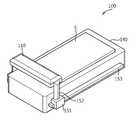
도 1은 본 발명에 따른 실런트 경화장치(100)의 개략적 사시도이다.1 is a schematic perspective view of a
도 1에 도시된 바와 같이, 본 발명의 따른 실런트 경화장치(100)는 기판 스테이지(140)와 엘이디 모듈(130; 도 2 참조)이 배열된 노광부(110), 그리고 노광부(110)를 기판 스테이지(140)의 면을 따라 구동시키는 구동부(151)로 구성되어 있다.As shown in FIG. 1, the
기판 스테이지(140)의 양측에는 기판 스테이지(140)의 상면과 평행하게 형성된 가이드바(153)가 형성될 수 있다. 가이드바(153) 중 어느 하나 또는 양쪽 모두의 가이드바(153)에는 노광부(110)를 기판(S) 면을 따라 이동하게 하는 구동부(150)가 설치될 수 있다. 그리고 구동부(151)의 상단 또는 측면에는 지지부(152)가 설치될 수 있다.
지지부(152)의 상단 또는 일측에는 노광부(110)가 설치될 수 있다. 이 때 노광부(110)는 노광부(110)에 배열된 엘이디 모듈(130)이 기판 스테이지(140)의 상면을 향하며, 기판 스테이지(140) 상에 안착되는 기판(S)으로부터 일정 간격 이격되도록 설치된다.An
기판 스테이지(140) 상에 안착되는 기판(S)과 노광부(110)의 저면 사이의 간격이 가까울수록 경화도(硬化度)는 향상되나, 실험에 의하면, 동일한 자외선 조사시간 하에서 간격이 30mm이하이면 경화도는 크게 차이가 없는 것으로 나타났다. 따라서 기판 스테이지(140) 상에 안착되는 기판(S)과 노광부(110)의 저면 사이의 간격은 약 30mm이하인 것이 바람직하다.As the distance between the substrate S seated on the
도 1에는 본 발명의 일실시예로 구동부(151)와 지지부(152)가 기판 스테이지(140)의 측면에 구비된 상태가 도시되어 있으나, 구동부(151)와 지지부(152)는 기판 스테이지(140)와 분리되어 설치될 수 있다. 예를 들면, 지지부(152)가 기판 스테이지(140) 주변에 설치되어 노광부(110)를 지지하고, 구동부(151)는 노광부(110)가 양 지지부(152) 사이를 수평 이동할 수 있게 구비되거나, 또는 노광부(110)와 지지부(152)를 일체로 수평 이동할 수 있게 구비될 수 있다.1 illustrates a state in which the
또한 도 1에는 본 발명의 일실시예로 노광부(110)가 기판(S) 위를 이동하며 노광하는 방식의 실런트 경화장치(100)가 도시되어 있으나, 노광부(110)가 기판(S) 전면(全面)을 일시에 노광할 수 있도록 노광부(110) 저면의 면적과 기판(S) 면적이 비슷하게 형성될 수 있다.In addition, FIG. 1 illustrates a
이하에서는 본 발명에 따른 노광부(110)에 대해 더욱 자세히 설명한다.Hereinafter, the
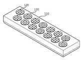
도 2는 본 발명의 제1 실시예에 따른 노광부(110)의 사시도이고, 도 3은 본 발명의 제1 실시예에 따른 노광부(110)의 저면도이며, 도 4는 본 발명의 제2 실시예에 따른 노광부(210)의 저면도이다.2 is a perspective view of an
도 2, 도 3 및 도 4에 도시된 바와 같이, 노광부(110)의 저면에는 하나 이상의 엘이디 소자(120)가 일정한 패턴으로 배열된 엘이디 모듈(130)이 복수 열로 배열되고, 이웃하는 열이 서로 평행한 채로 어긋나게 배열될 수 있다.As shown in FIGS. 2, 3, and 4, the
더욱 구체적으로 설명하면, 도 3에 도시된 바와 같이, 제1열을 구성하는 엘이디 모듈(131a, 131b) 사이의 간격을 D라 하고 제1열의 엘이디 모듈(131)이 배열되는 방향을 X방향이라 하면, 제1열과 이웃하는 제2열의 최초 엘이디 모듈(132a)은 제1열의 최초 엘이디 모듈(131a)보다 X방향으로
또는 도 4에 도시된 바와 같이, 제1열과 이웃하는 제2열의 최초 엘이디 모듈(232a)은 제1열의 최초 엘이디 모듈(231a)보다

같은 방법으로 제2열은


엘이디 소자에서 방출되는 빛은 직진성이 강해서 엘이디 모듈이 배치되지 않은 부분(예를 들면 이웃하는 엘이디 모듈간의 간격에 해당되는 부분)에 대응되는 노광면에는 자외선이 충분히 도달되지 않을 수 있다.Since the light emitted from the LED element is linear, the ultraviolet ray may not reach the exposure surface corresponding to the portion where the LED module is not disposed (for example, the portion corresponding to the gap between neighboring LED modules).
특히 노광부가 기판(S) 면을 따라 이동하며 노광하는 방식의 노광장치의 경우, 이웃하는 엘이디 모듈을 정사각형 또는 직사각형 형태로 배열하면, 엘이디 모듈이 지나가는 부분과 지나가지 않는 부분이 구별되어, 노광 후에 기판(S) 상에 자외선 광원이 충분히 도달되는 층과 그렇지 않은 층이 형성되고, 결과적으로 실런트의 경화상태가 균일하지 않게 된다.In particular, in the case of an exposure apparatus in which the exposure unit moves along the surface of the substrate S and exposes the light, the neighboring LED modules are arranged in a square or rectangular shape so that the portions through which the LED modules pass and those that do not pass are distinguished. On the substrate S, a layer in which the ultraviolet light source is sufficiently reached and a layer not being formed are formed, and as a result, the curing state of the sealant is not uniform.
이를 방지하기 위해 노광부와 노광면 사이의 거리를 멀리하면, 상기와 같은 문제를 어느 정도 보완할 수 있으나, 노광면에 도달되는 에너지가 전체적으로 급격히 줄어들게 되므로 광원의 출력을 높여야 하는 문제가 있다.In order to prevent this, when the distance between the exposure unit and the exposure surface is far, the above problem can be compensated to some extent, but the energy reaching the exposure surface is sharply reduced as a whole.
따라서 도 3에 도시된 바와 같이, 엘이디 모듈(130)을 배열하면, 노광부(110)와 노광면 사이의 거리를 충분히 가깝게 유지하더라도, 노광면에 자외선이 균일하게 조사될 수 있다.Therefore, as shown in FIG. 3, when the
엘이디 모듈(130)을 도 3에 도시한 바와 같이 배열하고 80mm의 폭을 갖는 노광부(110)를 수평 이동시키며 노광면에 도달되는 자외선 에너지를 측정한 결과, 노광부(110)의 폭인 80mm 구간에서 측정된 대부분의 에너지가 해당 구간의 평균치를 기준으로 ±5% 범위에 있을 정도로 균일함을 알 수 있었다.The
따라서 본 발명에 따른 엘이디 모듈(130)의 배열구조에 의하면, 노광부(110)와 노광면 사이의 거리를 충분히 가깝게 하더라고 노광면에 균일하게 에너지가 전달되고, 노광부(110)와 노광면 사이의 거리가 가까워 종전에 비해 노광부(110)의 출력을 낮추어도 충분한 노광효과를 얻을 수 있어, 소비되는 전력을 줄일 수 있다. 이에 의해 엘이디 소자(120)에서 발생되는 열을 감소시킴과 동시에 엘이디 소자(120)의 수명을 연장시킬 수 있다.
Therefore, according to the arrangement of the
이하에서는 상술한 바와 같은 구성의 본 실시예에 따른 실런트 경화장치(100)의 작동상태를 설명하기로 한다.Hereinafter, the operating state of the
실런트 경화장치(100)가 구비된 챔버(미도시)내로 마스크가 반입되어 챔버 상부에 구비된 흡착척(미도시)에 흡착된다. 마스크는 실런트가 도포된 부분에만 자외선이 도달되게 한다. 따라서 마스크에는 실런트가 도포된 패턴에 대응되는 패턴으로 창(窓)이 형성되어 있다.The mask is brought into a chamber (not shown) provided with the
마스크의 반입 및 흡착이 완료된 후, 실런트가 사이에 도포된 채 합착된 기판(S)이 기판 스테이지(140) 위에 안착된다. 기판(S)은 합착장치에서 합착된 후, 로봇(미도시)에 의해 실런트 경화장치(100)가 구비된 챔버(미도시)내로 반입될 수도 있고, 노광부(110)를 구비하고 있는 합착장치에서 합착 후, 기판 스테이지(140)에 안착된 상태일 수 있다.After the loading and adsorption of the mask is completed, the bonded substrate S is seated on the
기판(S)이 기판 스테이지(140) 위에 안착된 후, 마스크와 기판(S)의 정렬이 이루어진다.After the substrate S is seated on the
그 후, 노광부(110)에 배열된 엘이디 모듈(130)은 점등되고, 구동부(151)가 가이드바(153)를 따라 이동하면, 노광부(110)는 기판(S) 면 및 기판 스테이지(140)의 면을 따라 마스크 위를 이동하며 자외선을 조사하여 실런트를 경화시킨다.Thereafter, the
상술한 바와 같은 과정이 완료되면, 경화가 완료된 기판(S)은 로봇(미도시)에 의해 반출되어 경화공정이 완료된다.
When the process as described above is completed, the hardened substrate S is carried out by a robot (not shown) to complete the hardening process.
앞에서 설명되고, 도면에 도시된 본 발명의 일 실시예는, 본 발명의 기술적 사상을 한정하는 것으로 해석되어서는 안 된다. 본 발명의 보호범위는 청구범위에 기재된 사항에 의하여만 제한되고, 본 발명의 기술분야에서 통상의 지식을 가진 자는 본 발명의 기술적 사상을 다양한 형태로 개량 변경하는 것이 가능하다. 따라서 이러한 개량 및 변경은 통상의 지식을 가진 자에게 자명한 것인 한 본 발명의 보호범위에 속하게 될 것이다.
One embodiment of the invention described above and shown in the drawings should not be construed as limiting the technical idea of the present invention. The scope of protection of the present invention is limited only by the matters described in the claims, and those skilled in the art will be able to modify the technical idea of the present invention in various forms. Accordingly, such improvements and modifications will fall within the scope of the present invention as long as they are obvious to those skilled in the art.
100: 실런트 경화장치
110, 210: 노광부
120: 엘이디 소자
130, 230: 엘이디 모듈
140: 기판 스테이지
151: 구동부
152: 지지부
153: 가이드부100: sealant curing device
110, 210: exposed portion
120: LED element
130, 230: LED module
140: substrate stage
151: drive unit
152: support
153: guide part
Claims (10)
Translated fromKorean상기 기판 스테이지 상면(上面)으로부터 소정 간격만큼 이격되어 위치하고, 저면에 엘이디 소자로 구성된 엘이디 모듈이 복수 열(列)로 배열되며, 상기 복수 열 중 이웃하는 열은 서로 평행한 채로 어긋나게 배열되는 노광부;
상기 노광부가 상기 기판 스테이지 상면(上面)으로부터 이격되도록, 상기 노광부를 지지하는 지지부; 및
상기 노광부가 상기 기판 스테이지 상에서 수평 이동하도록 상기 지지부를 수평 이동시키는 구동부를 포함하고,
복수 개의 상기 엘이디 모듈이 배열되는 열 방향을 X방향이라 할 때 상기 X방향을 따라 복수 열의 상기 엘이디 모듈은 제1열 및 제2열을 포함하며,
상기 제1열 및 상기 제2열로 배열되는 복수 개의 상기 엘이디 모듈의 중심에 대한 상호 간격을 D라 할 때, 상기 X방향을 따라 상기 제1열을 시작하는 상기 엘이디 모듈의 중심에 대해 상기 제2열로 시작하는 상기 엘이디 모듈의 중심은

A substrate stage on which a sealant-coated substrate is seated;
The exposure unit is spaced apart from the upper surface of the substrate stage by a predetermined interval, and an LED module composed of LED elements is arranged in a plurality of rows, and adjacent columns among the plurality of rows are arranged to be displaced in parallel with each other. ;
A support part supporting the exposure part such that the exposure part is spaced apart from an upper surface of the substrate stage; And
A driving part horizontally moving the support part such that the exposure part horizontally moves on the substrate stage;
When the column direction in which the plurality of LED modules are arranged is referred to as the X direction, the LED modules of the plurality of rows along the X direction include a first row and a second row,
When the mutual spacing between the centers of the plurality of LED modules arranged in the first column and the second column is D, the second column is relative to the center of the LED module starting the first column along the X direction. The center of the LED module starting with the column
상기 엘이디 모듈 중 인접하는 임의의 3개의 상기 엘이디 모듈은 서로 간의 간격이 동일한 것을 특징으로 하는 실런트 경화장치.
The method of claim 1,
Sealant curing apparatus, characterized in that any of the three adjacent LED module of the LED module is equal to each other.
복수 개의 상기 엘이디 모듈이 배열되는 열 방향을 X방향이라 할 때 상기 X방향을 따라 복수 열의 상기 엘이디 모듈은 제1열, 제2열 및 제3열을 포함하며,
상기 제1열, 상기 제2열 및 상기 제3열로 배열되는 복수 개의 상기 엘이디 모듈의 중심에 대한 상호 간격을 D라 할 때,
상기 X방향을 따라 상기 제1열을 시작하는 상기 엘이디 모듈의 중심에 대해 상기 제2열로 시작하는 상기 엘이디 모듈의 중심은

상기 X방향을 따라 상기 제1열을 시작하는 상기 엘이디 모듈의 중심에 대해 상기 제3열로 시작하는 상기 엘이디 모듈의 중심은

The method of claim 1,
When the column direction in which the plurality of LED modules are arranged is referred to as the X direction, the plurality of columns of the LED modules along the X direction include a first row, a second row, and a third row,
When the mutual spacing between the centers of the plurality of LED modules arranged in the first column, the second column and the third column is D,
The center of the LED module starting with the second column with respect to the center of the LED module starting the first column along the X direction is
The center of the LED module starting with the third column with respect to the center of the LED module starting the first column along the X direction is
상기 엘이디 소자는 자외선을 방출하는 엘이디 소자인 것을 특징으로 하는 실런트 경화장치.
The method of claim 1,
The LED device is a sealant curing apparatus, characterized in that the LED device for emitting ultraviolet light.
복수 개의 상기 엘이디 모듈이 배열되는 열 방향을 X방향이라 할 때 상기 X방향을 따라 복수 열의 상기 엘이디 모듈은 제1열 및 제2열을 포함하며,
상기 제1열 및 상기 제2열로 배열되는 복수 개의 상기 엘이디 모듈의 중심에 대한 상호 간격을 D라 할 때, 상기 X방향을 따라 상기 제1열을 시작하는 상기 엘이디 모듈의 중심에 대해 상기 제2열로 시작하는 상기 엘이디 모듈의 중심은

LED modules composed of LED elements spaced apart from each other and horizontally moved along the plate surface of the substrate are arranged in a plurality of rows, and neighboring columns are arranged to be displaced in parallel with each other,
When the column direction in which the plurality of LED modules are arranged is referred to as the X direction, the plurality of columns of the LED modules along the X direction include a first row and a second row,
When the mutual spacing between the centers of the plurality of LED modules arranged in the first column and the second column is D, the second column is relative to the center of the LED module starting the first column along the X direction. The center of the LED module starting with the column
상기 엘이디 모듈 중 인접하는 임의의 3개의 상기 엘이디 모듈은 서로 간의 간격이 동일한 것을 특징으로 하는 실런트 경화장치용 엘이디 배열방법.
The method of claim 7, wherein
And any three adjacent LED modules adjacent to each other of the LED modules are equal to each other.
복수 개의 상기 엘이디 모듈이 배열되는 열 방향을 X방향이라 할 때 상기 X방향을 따라 복수 열의 상기 엘이디 모듈은 제1열, 제2열 및 제3열을 포함하며,
상기 제1열, 상기 제2열 및 상기 제3열로 배열되는 복수 개의 상기 엘이디 모듈의 중심에 대한 상호 간격을 D라 할 때,
상기 X방향을 따라 상기 제1열을 시작하는 상기 엘이디 모듈의 중심에 대해 상기 제2열로 시작하는 상기 엘이디 모듈의 중심은

상기 X방향을 따라 상기 제1열을 시작하는 상기 엘이디 모듈의 중심에 대해 상기 제3열로 시작하는 상기 엘이디 모듈의 중심은

When the column direction in which the plurality of LED modules are arranged is referred to as the X direction, the plurality of columns of the LED modules along the X direction include a first row, a second row, and a third row,
When the mutual spacing between the centers of the plurality of LED modules arranged in the first column, the second column and the third column is D,
The center of the LED module starting with the second column with respect to the center of the LED module starting the first column along the X direction is
The center of the LED module starting with the third column with respect to the center of the LED module starting the first column along the X direction is
Priority Applications (1)
| Application Number | Priority Date | Filing Date | Title |
|---|---|---|---|
| KR1020100097515AKR101367665B1 (en) | 2010-10-06 | 2010-10-06 | Sealant curing apparatus and arrangement method of LED for sealant curing apparatus |
Applications Claiming Priority (1)
| Application Number | Priority Date | Filing Date | Title |
|---|---|---|---|
| KR1020100097515AKR101367665B1 (en) | 2010-10-06 | 2010-10-06 | Sealant curing apparatus and arrangement method of LED for sealant curing apparatus |
Publications (2)
| Publication Number | Publication Date |
|---|---|
| KR20120035782A KR20120035782A (en) | 2012-04-16 |
| KR101367665B1true KR101367665B1 (en) | 2014-02-28 |
Family
ID=46137630
Family Applications (1)
| Application Number | Title | Priority Date | Filing Date |
|---|---|---|---|
| KR1020100097515AExpired - Fee RelatedKR101367665B1 (en) | 2010-10-06 | 2010-10-06 | Sealant curing apparatus and arrangement method of LED for sealant curing apparatus |
Country Status (1)
| Country | Link |
|---|---|
| KR (1) | KR101367665B1 (en) |
Families Citing this family (3)
| Publication number | Priority date | Publication date | Assignee | Title |
|---|---|---|---|---|
| KR102137427B1 (en)* | 2014-01-02 | 2020-07-24 | 엘지이노텍 주식회사 | Light emitting device lamp |
| KR102247826B1 (en)* | 2014-06-27 | 2021-05-03 | 엘지디스플레이 주식회사 | A display device hardening apparatus and methode of hardening adhesive material using the same |
| JP2018521884A (en) | 2015-07-20 | 2018-08-09 | スリーエム イノベイティブ プロパティズ カンパニー | Actinic radiation equipment for rapid curing of resins |
Citations (4)
| Publication number | Priority date | Publication date | Assignee | Title |
|---|---|---|---|---|
| KR20060050158A (en)* | 2004-07-16 | 2006-05-19 | 가부시키가이샤 엔프라스 | Surface light source device, lighting unit and beam control member |
| KR20070019975A (en)* | 2004-01-07 | 2007-02-16 | 컨트롤 큐어, 인코포레이티드 | Rotary shock hardening method and device |
| KR100787904B1 (en)* | 2005-08-09 | 2007-12-27 | 세이코 엡슨 가부시키가이샤 | Electro-optical devices and electronic devices |
| JP2011005787A (en)* | 2009-06-26 | 2011-01-13 | Noritsu Koki Co Ltd | Ultraviolet light source unit |
- 2010
- 2010-10-06KRKR1020100097515Apatent/KR101367665B1/ennot_activeExpired - Fee Related
Patent Citations (4)
| Publication number | Priority date | Publication date | Assignee | Title |
|---|---|---|---|---|
| KR20070019975A (en)* | 2004-01-07 | 2007-02-16 | 컨트롤 큐어, 인코포레이티드 | Rotary shock hardening method and device |
| KR20060050158A (en)* | 2004-07-16 | 2006-05-19 | 가부시키가이샤 엔프라스 | Surface light source device, lighting unit and beam control member |
| KR100787904B1 (en)* | 2005-08-09 | 2007-12-27 | 세이코 엡슨 가부시키가이샤 | Electro-optical devices and electronic devices |
| JP2011005787A (en)* | 2009-06-26 | 2011-01-13 | Noritsu Koki Co Ltd | Ultraviolet light source unit |
Also Published As
| Publication number | Publication date |
|---|---|
| KR20120035782A (en) | 2012-04-16 |
Similar Documents
| Publication | Publication Date | Title |
|---|---|---|
| US20120145928A1 (en) | Ultraviolet curing device for liquid crystal panel and curing method therefor | |
| KR101722026B1 (en) | A flat display panel, a mother substrate for the flat display panel, and a method for manufacturing the flat display panel | |
| KR101930041B1 (en) | Photoirradiation device | |
| JP5180439B2 (en) | Ultraviolet light irradiation apparatus and irradiation method, substrate manufacturing apparatus and substrate manufacturing method | |
| CN105026823A (en) | Light irradiation device | |
| KR101312094B1 (en) | UV Curing device using LED | |
| CN102023417A (en) | Light irradiation apparatus | |
| CN106024670A (en) | Heater block and substrate processing apparatus | |
| TWI543228B (en) | Light irradiation device | |
| KR101367665B1 (en) | Sealant curing apparatus and arrangement method of LED for sealant curing apparatus | |
| WO2012011166A1 (en) | Light irradiation device | |
| JP2007334039A (en) | Light source device and method of panel alignment using the same | |
| KR101350924B1 (en) | Sealant Curing Device | |
| KR100539168B1 (en) | Sealant curing apparatus for sealing of LCD panel | |
| JP6314604B2 (en) | Irradiation device | |
| KR20170014484A (en) | Ultra Violet Light Source Module | |
| KR100916966B1 (en) | LCD manufacturing device | |
| KR20150121511A (en) | Ultra violet cure apparatus using leds | |
| KR101460018B1 (en) | Uv curing apparatus | |
| KR20120068804A (en) | Sealant curing apparatus | |
| JP2010266616A (en) | Light irradiation device | |
| EP2151711A1 (en) | Liquid crystal sealing apparatus | |
| KR100931320B1 (en) | UV curing device for flat panel display liquid crystal manufacturing | |
| JP2007057861A (en) | Square-shaped condensing optical system and ultraviolet irradiation device for liquid crystal panel | |
| CN113228317A (en) | Light emitting diode, manufacturing method thereof, light emitting diode module and display device |
Legal Events
| Date | Code | Title | Description |
|---|---|---|---|
| A201 | Request for examination | ||
| PA0109 | Patent application | St.27 status event code:A-0-1-A10-A12-nap-PA0109 | |
| PA0201 | Request for examination | St.27 status event code:A-1-2-D10-D11-exm-PA0201 | |
| PG1501 | Laying open of application | St.27 status event code:A-1-1-Q10-Q12-nap-PG1501 | |
| D13-X000 | Search requested | St.27 status event code:A-1-2-D10-D13-srh-X000 | |
| D14-X000 | Search report completed | St.27 status event code:A-1-2-D10-D14-srh-X000 | |
| E902 | Notification of reason for refusal | ||
| PE0902 | Notice of grounds for rejection | St.27 status event code:A-1-2-D10-D21-exm-PE0902 | |
| T11-X000 | Administrative time limit extension requested | St.27 status event code:U-3-3-T10-T11-oth-X000 | |
| E13-X000 | Pre-grant limitation requested | St.27 status event code:A-2-3-E10-E13-lim-X000 | |
| P11-X000 | Amendment of application requested | St.27 status event code:A-2-2-P10-P11-nap-X000 | |
| P13-X000 | Application amended | St.27 status event code:A-2-2-P10-P13-nap-X000 | |
| R17-X000 | Change to representative recorded | St.27 status event code:A-3-3-R10-R17-oth-X000 | |
| E90F | Notification of reason for final refusal | ||
| PE0902 | Notice of grounds for rejection | St.27 status event code:A-1-2-D10-D21-exm-PE0902 | |
| E13-X000 | Pre-grant limitation requested | St.27 status event code:A-2-3-E10-E13-lim-X000 | |
| P11-X000 | Amendment of application requested | St.27 status event code:A-2-2-P10-P11-nap-X000 | |
| P13-X000 | Application amended | St.27 status event code:A-2-2-P10-P13-nap-X000 | |
| E701 | Decision to grant or registration of patent right | ||
| PE0701 | Decision of registration | St.27 status event code:A-1-2-D10-D22-exm-PE0701 | |
| PN2301 | Change of applicant | St.27 status event code:A-3-3-R10-R13-asn-PN2301 St.27 status event code:A-3-3-R10-R11-asn-PN2301 | |
| GRNT | Written decision to grant | ||
| PR0701 | Registration of establishment | St.27 status event code:A-2-4-F10-F11-exm-PR0701 | |
| PR1002 | Payment of registration fee | St.27 status event code:A-2-2-U10-U11-oth-PR1002 Fee payment year number:1 | |
| PG1601 | Publication of registration | St.27 status event code:A-4-4-Q10-Q13-nap-PG1601 | |
| PN2301 | Change of applicant | St.27 status event code:A-5-5-R10-R13-asn-PN2301 St.27 status event code:A-5-5-R10-R11-asn-PN2301 | |
| PN2301 | Change of applicant | St.27 status event code:A-5-5-R10-R13-asn-PN2301 St.27 status event code:A-5-5-R10-R11-asn-PN2301 | |
| PN2301 | Change of applicant | St.27 status event code:A-5-5-R10-R13-asn-PN2301 St.27 status event code:A-5-5-R10-R11-asn-PN2301 | |
| P22-X000 | Classification modified | St.27 status event code:A-4-4-P10-P22-nap-X000 | |
| LAPS | Lapse due to unpaid annual fee | ||
| PC1903 | Unpaid annual fee | St.27 status event code:A-4-4-U10-U13-oth-PC1903 Not in force date:20170221 Payment event data comment text:Termination Category : DEFAULT_OF_REGISTRATION_FEE | |
| PC1903 | Unpaid annual fee | St.27 status event code:N-4-6-H10-H13-oth-PC1903 Ip right cessation event data comment text:Termination Category : DEFAULT_OF_REGISTRATION_FEE Not in force date:20170221 | |
| P22-X000 | Classification modified | St.27 status event code:A-4-4-P10-P22-nap-X000 | |
| P22-X000 | Classification modified | St.27 status event code:A-4-4-P10-P22-nap-X000 | |
| R18-X000 | Changes to party contact information recorded | St.27 status event code:A-5-5-R10-R18-oth-X000 |