KR101356695B1 - Method of fabricating semiconductor device - Google Patents
Method of fabricating semiconductor deviceDownload PDFInfo
- Publication number
- KR101356695B1 KR101356695B1KR1020070078706AKR20070078706AKR101356695B1KR 101356695 B1KR101356695 B1KR 101356695B1KR 1020070078706 AKR1020070078706 AKR 1020070078706AKR 20070078706 AKR20070078706 AKR 20070078706AKR 101356695 B1KR101356695 B1KR 101356695B1
- Authority
- KR
- South Korea
- Prior art keywords
- insulating film
- semiconductor device
- vapor deposition
- delete delete
- manufacturing
- Prior art date
- Legal status (The legal status is an assumption and is not a legal conclusion. Google has not performed a legal analysis and makes no representation as to the accuracy of the status listed.)
- Active
Links
Images


Classifications
- H—ELECTRICITY
- H10—SEMICONDUCTOR DEVICES; ELECTRIC SOLID-STATE DEVICES NOT OTHERWISE PROVIDED FOR
- H10D—INORGANIC ELECTRIC SEMICONDUCTOR DEVICES
- H10D64/00—Electrodes of devices having potential barriers
- H10D64/60—Electrodes characterised by their materials
- H10D64/66—Electrodes having a conductor capacitively coupled to a semiconductor by an insulator, e.g. MIS electrodes
- H10D64/675—Gate sidewall spacers
- H10D64/679—Gate sidewall spacers comprising air gaps
- H—ELECTRICITY
- H01—ELECTRIC ELEMENTS
- H01L—SEMICONDUCTOR DEVICES NOT COVERED BY CLASS H10
- H01L21/00—Processes or apparatus adapted for the manufacture or treatment of semiconductor or solid state devices or of parts thereof
- H01L21/02—Manufacture or treatment of semiconductor devices or of parts thereof
- H01L21/04—Manufacture or treatment of semiconductor devices or of parts thereof the devices having potential barriers, e.g. a PN junction, depletion layer or carrier concentration layer
- H01L21/18—Manufacture or treatment of semiconductor devices or of parts thereof the devices having potential barriers, e.g. a PN junction, depletion layer or carrier concentration layer the devices having semiconductor bodies comprising elements of Group IV of the Periodic Table or AIIIBV compounds with or without impurities, e.g. doping materials
- H01L21/30—Treatment of semiconductor bodies using processes or apparatus not provided for in groups H01L21/20 - H01L21/26
- H01L21/31—Treatment of semiconductor bodies using processes or apparatus not provided for in groups H01L21/20 - H01L21/26 to form insulating layers thereon, e.g. for masking or by using photolithographic techniques; After treatment of these layers; Selection of materials for these layers
- C—CHEMISTRY; METALLURGY
- C23—COATING METALLIC MATERIAL; COATING MATERIAL WITH METALLIC MATERIAL; CHEMICAL SURFACE TREATMENT; DIFFUSION TREATMENT OF METALLIC MATERIAL; COATING BY VACUUM EVAPORATION, BY SPUTTERING, BY ION IMPLANTATION OR BY CHEMICAL VAPOUR DEPOSITION, IN GENERAL; INHIBITING CORROSION OF METALLIC MATERIAL OR INCRUSTATION IN GENERAL
- C23C—COATING METALLIC MATERIAL; COATING MATERIAL WITH METALLIC MATERIAL; SURFACE TREATMENT OF METALLIC MATERIAL BY DIFFUSION INTO THE SURFACE, BY CHEMICAL CONVERSION OR SUBSTITUTION; COATING BY VACUUM EVAPORATION, BY SPUTTERING, BY ION IMPLANTATION OR BY CHEMICAL VAPOUR DEPOSITION, IN GENERAL
- C23C16/00—Chemical coating by decomposition of gaseous compounds, without leaving reaction products of surface material in the coating, i.e. chemical vapour deposition [CVD] processes
- C23C16/22—Chemical coating by decomposition of gaseous compounds, without leaving reaction products of surface material in the coating, i.e. chemical vapour deposition [CVD] processes characterised by the deposition of inorganic material, other than metallic material
- C23C16/30—Deposition of compounds, mixtures or solid solutions, e.g. borides, carbides, nitrides
- C23C16/40—Oxides
- C23C16/401—Oxides containing silicon
- C23C16/402—Silicon dioxide
- H—ELECTRICITY
- H01—ELECTRIC ELEMENTS
- H01L—SEMICONDUCTOR DEVICES NOT COVERED BY CLASS H10
- H01L21/00—Processes or apparatus adapted for the manufacture or treatment of semiconductor or solid state devices or of parts thereof
- H01L21/02—Manufacture or treatment of semiconductor devices or of parts thereof
- H01L21/02104—Forming layers
- H01L21/02107—Forming insulating materials on a substrate
- H01L21/02109—Forming insulating materials on a substrate characterised by the type of layer, e.g. type of material, porous/non-porous, pre-cursors, mixtures or laminates
- H01L21/02112—Forming insulating materials on a substrate characterised by the type of layer, e.g. type of material, porous/non-porous, pre-cursors, mixtures or laminates characterised by the material of the layer
- H01L21/02123—Forming insulating materials on a substrate characterised by the type of layer, e.g. type of material, porous/non-porous, pre-cursors, mixtures or laminates characterised by the material of the layer the material containing silicon
- H01L21/02126—Forming insulating materials on a substrate characterised by the type of layer, e.g. type of material, porous/non-porous, pre-cursors, mixtures or laminates characterised by the material of the layer the material containing silicon the material containing Si, O, and at least one of H, N, C, F, or other non-metal elements, e.g. SiOC, SiOC:H or SiONC
- H—ELECTRICITY
- H01—ELECTRIC ELEMENTS
- H01L—SEMICONDUCTOR DEVICES NOT COVERED BY CLASS H10
- H01L21/00—Processes or apparatus adapted for the manufacture or treatment of semiconductor or solid state devices or of parts thereof
- H01L21/02—Manufacture or treatment of semiconductor devices or of parts thereof
- H01L21/02104—Forming layers
- H01L21/02107—Forming insulating materials on a substrate
- H01L21/02296—Forming insulating materials on a substrate characterised by the treatment performed before or after the formation of the layer
- H01L21/02318—Forming insulating materials on a substrate characterised by the treatment performed before or after the formation of the layer post-treatment
- H01L21/02362—Forming insulating materials on a substrate characterised by the treatment performed before or after the formation of the layer post-treatment formation of intermediate layers, e.g. capping layers or diffusion barriers
- H—ELECTRICITY
- H01—ELECTRIC ELEMENTS
- H01L—SEMICONDUCTOR DEVICES NOT COVERED BY CLASS H10
- H01L21/00—Processes or apparatus adapted for the manufacture or treatment of semiconductor or solid state devices or of parts thereof
- H01L21/70—Manufacture or treatment of devices consisting of a plurality of solid state components formed in or on a common substrate or of parts thereof; Manufacture of integrated circuit devices or of parts thereof
- H01L21/71—Manufacture of specific parts of devices defined in group H01L21/70
- H01L21/76—Making of isolation regions between components
- H01L21/764—Air gaps
- H—ELECTRICITY
- H01—ELECTRIC ELEMENTS
- H01L—SEMICONDUCTOR DEVICES NOT COVERED BY CLASS H10
- H01L21/00—Processes or apparatus adapted for the manufacture or treatment of semiconductor or solid state devices or of parts thereof
- H01L21/70—Manufacture or treatment of devices consisting of a plurality of solid state components formed in or on a common substrate or of parts thereof; Manufacture of integrated circuit devices or of parts thereof
- H01L21/71—Manufacture of specific parts of devices defined in group H01L21/70
- H01L21/768—Applying interconnections to be used for carrying current between separate components within a device comprising conductors and dielectrics
- H01L21/76801—Applying interconnections to be used for carrying current between separate components within a device comprising conductors and dielectrics characterised by the formation and the after-treatment of the dielectrics, e.g. smoothing
- H01L21/7682—Applying interconnections to be used for carrying current between separate components within a device comprising conductors and dielectrics characterised by the formation and the after-treatment of the dielectrics, e.g. smoothing the dielectric comprising air gaps
- H—ELECTRICITY
- H10—SEMICONDUCTOR DEVICES; ELECTRIC SOLID-STATE DEVICES NOT OTHERWISE PROVIDED FOR
- H10B—ELECTRONIC MEMORY DEVICES
- H10B41/00—Electrically erasable-and-programmable ROM [EEPROM] devices comprising floating gates
- H10B41/30—Electrically erasable-and-programmable ROM [EEPROM] devices comprising floating gates characterised by the memory core region
- H—ELECTRICITY
- H10—SEMICONDUCTOR DEVICES; ELECTRIC SOLID-STATE DEVICES NOT OTHERWISE PROVIDED FOR
- H10B—ELECTRONIC MEMORY DEVICES
- H10B43/00—EEPROM devices comprising charge-trapping gate insulators
- H10B43/30—EEPROM devices comprising charge-trapping gate insulators characterised by the memory core region
- H—ELECTRICITY
- H10—SEMICONDUCTOR DEVICES; ELECTRIC SOLID-STATE DEVICES NOT OTHERWISE PROVIDED FOR
- H10D—INORGANIC ELECTRIC SEMICONDUCTOR DEVICES
- H10D64/00—Electrodes of devices having potential barriers
- H10D64/01—Manufacture or treatment
- H10D64/031—Manufacture or treatment of data-storage electrodes
- H10D64/035—Manufacture or treatment of data-storage electrodes comprising conductor-insulator-conductor-insulator-semiconductor structures
- H—ELECTRICITY
- H10—SEMICONDUCTOR DEVICES; ELECTRIC SOLID-STATE DEVICES NOT OTHERWISE PROVIDED FOR
- H10D—INORGANIC ELECTRIC SEMICONDUCTOR DEVICES
- H10D64/00—Electrodes of devices having potential barriers
- H10D64/01—Manufacture or treatment
- H10D64/031—Manufacture or treatment of data-storage electrodes
- H10D64/037—Manufacture or treatment of data-storage electrodes comprising charge-trapping insulators
- H—ELECTRICITY
- H10—SEMICONDUCTOR DEVICES; ELECTRIC SOLID-STATE DEVICES NOT OTHERWISE PROVIDED FOR
- H10D—INORGANIC ELECTRIC SEMICONDUCTOR DEVICES
- H10D64/00—Electrodes of devices having potential barriers
- H10D64/60—Electrodes characterised by their materials
- H10D64/66—Electrodes having a conductor capacitively coupled to a semiconductor by an insulator, e.g. MIS electrodes
- H10D64/671—Electrodes having a conductor capacitively coupled to a semiconductor by an insulator, e.g. MIS electrodes the conductor having lateral variation in doping or structure
- H—ELECTRICITY
- H01—ELECTRIC ELEMENTS
- H01L—SEMICONDUCTOR DEVICES NOT COVERED BY CLASS H10
- H01L21/00—Processes or apparatus adapted for the manufacture or treatment of semiconductor or solid state devices or of parts thereof
- H01L21/02—Manufacture or treatment of semiconductor devices or of parts thereof
- H01L21/02104—Forming layers
- H01L21/02107—Forming insulating materials on a substrate
- H01L21/02109—Forming insulating materials on a substrate characterised by the type of layer, e.g. type of material, porous/non-porous, pre-cursors, mixtures or laminates
- H01L21/02112—Forming insulating materials on a substrate characterised by the type of layer, e.g. type of material, porous/non-porous, pre-cursors, mixtures or laminates characterised by the material of the layer
- H01L21/02123—Forming insulating materials on a substrate characterised by the type of layer, e.g. type of material, porous/non-porous, pre-cursors, mixtures or laminates characterised by the material of the layer the material containing silicon
- H01L21/02164—Forming insulating materials on a substrate characterised by the type of layer, e.g. type of material, porous/non-porous, pre-cursors, mixtures or laminates characterised by the material of the layer the material containing silicon the material being a silicon oxide, e.g. SiO2
- H—ELECTRICITY
- H01—ELECTRIC ELEMENTS
- H01L—SEMICONDUCTOR DEVICES NOT COVERED BY CLASS H10
- H01L21/00—Processes or apparatus adapted for the manufacture or treatment of semiconductor or solid state devices or of parts thereof
- H01L21/02—Manufacture or treatment of semiconductor devices or of parts thereof
- H01L21/02104—Forming layers
- H01L21/02107—Forming insulating materials on a substrate
- H01L21/02109—Forming insulating materials on a substrate characterised by the type of layer, e.g. type of material, porous/non-porous, pre-cursors, mixtures or laminates
- H01L21/02205—Forming insulating materials on a substrate characterised by the type of layer, e.g. type of material, porous/non-porous, pre-cursors, mixtures or laminates the layer being characterised by the precursor material for deposition
- H01L21/02208—Forming insulating materials on a substrate characterised by the type of layer, e.g. type of material, porous/non-porous, pre-cursors, mixtures or laminates the layer being characterised by the precursor material for deposition the precursor containing a compound comprising Si
- H01L21/02211—Forming insulating materials on a substrate characterised by the type of layer, e.g. type of material, porous/non-porous, pre-cursors, mixtures or laminates the layer being characterised by the precursor material for deposition the precursor containing a compound comprising Si the compound being a silane, e.g. disilane, methylsilane or chlorosilane
- H—ELECTRICITY
- H01—ELECTRIC ELEMENTS
- H01L—SEMICONDUCTOR DEVICES NOT COVERED BY CLASS H10
- H01L21/00—Processes or apparatus adapted for the manufacture or treatment of semiconductor or solid state devices or of parts thereof
- H01L21/02—Manufacture or treatment of semiconductor devices or of parts thereof
- H01L21/02104—Forming layers
- H01L21/02107—Forming insulating materials on a substrate
- H01L21/02225—Forming insulating materials on a substrate characterised by the process for the formation of the insulating layer
- H01L21/0226—Forming insulating materials on a substrate characterised by the process for the formation of the insulating layer formation by a deposition process
- H01L21/02263—Forming insulating materials on a substrate characterised by the process for the formation of the insulating layer formation by a deposition process deposition from the gas or vapour phase
- H01L21/02271—Forming insulating materials on a substrate characterised by the process for the formation of the insulating layer formation by a deposition process deposition from the gas or vapour phase deposition by decomposition or reaction of gaseous or vapour phase compounds, i.e. chemical vapour deposition
- H01L21/02274—Forming insulating materials on a substrate characterised by the process for the formation of the insulating layer formation by a deposition process deposition from the gas or vapour phase deposition by decomposition or reaction of gaseous or vapour phase compounds, i.e. chemical vapour deposition in the presence of a plasma [PECVD]
Landscapes
- Engineering & Computer Science (AREA)
- Chemical & Material Sciences (AREA)
- Physics & Mathematics (AREA)
- Condensed Matter Physics & Semiconductors (AREA)
- General Physics & Mathematics (AREA)
- Manufacturing & Machinery (AREA)
- Computer Hardware Design (AREA)
- Microelectronics & Electronic Packaging (AREA)
- Power Engineering (AREA)
- General Chemical & Material Sciences (AREA)
- Inorganic Chemistry (AREA)
- Chemical Kinetics & Catalysis (AREA)
- Materials Engineering (AREA)
- Mechanical Engineering (AREA)
- Metallurgy (AREA)
- Organic Chemistry (AREA)
- Formation Of Insulating Films (AREA)
- Internal Circuitry In Semiconductor Integrated Circuit Devices (AREA)
- Semiconductor Memories (AREA)
- Non-Volatile Memory (AREA)
Abstract
Translated fromKoreanDescription
Translated fromKorean본 발명은 반도체 소자의 제조 방법에 관한 것으로서, 더욱 상세하게는, 반도체 소자의 배선들 또는 게이트 스택을 고립화시키는 에어 갭을 갖는 절연막의 형성 방법에 관한 것이다.BACKGROUND OF THE INVENTION 1. Field of the Invention The present invention relates to a method of manufacturing a semiconductor device, and more particularly, to a method of forming an insulating film having an air gap to isolate wirings or gate stacks of a semiconductor device.
반도체 장치, 예를 들면, 로직 소자, 디램 및 플래시 메모리 등이 고집적화 됨에 따라, 이를 구성하는 금속 배선들 사이의 간격이 점차 협소해지고 있다. 상기 금속 배선들과 이들을 고립화시키는 절연막에 의해 발생하는 기생 캐패시턴스에 의한 용량성 결합(capacitive coupling)은 배선간 지연(interconnection delay)을 초래하여 반도체 장치의 집적화 및 고속화에 대한 중대로 장애로 인식되고 있다.As semiconductor devices, for example, logic devices, DRAMs, flash memories, and the like are highly integrated, the gaps between the metal wires constituting the semiconductor devices are becoming narrower. Capacitive coupling due to parasitic capacitance generated by the metal wires and the insulating film that isolates them causes an interconnection delay and is recognized as a serious obstacle to the integration and speed of semiconductor devices. .
상기 배선간 지연 현상 이외에도, 플래시 메모리 소자의 인접한 셀들의 게이트 스택 사이에도 용량성 결합(capacitive coupling)에 의한 신호 간섭이 발생할 수 있다. 예를 들면, 플래시 메모리에서, 선택된 플래시 메모리 셀에 대한 프로그래밍 또는 읽기 동작시, 선택되지 않은 플래시 메모리 셀과의 용량성 결합 때문에 상기 프로그래밍 또는 읽기 동작이 실패하는 경우가 있다.In addition to the inter-wire delay, signal interference due to capacitive coupling may also occur between gate stacks of adjacent cells of the flash memory device. For example, in flash memory, during a programming or reading operation on a selected flash memory cell, the programming or reading operation may fail due to capacitive coupling with an unselected flash memory cell.
상기 인접한 금속 배선들 또는 메모리 셀들 사이에서 발생하는 기생 캐패시 턴스에 의한 용량성 결합을 감소시키기 위해, 절연막으로서 저유전율 물질을 사용하거나 절연막 내에 에어 갭(air gap) 또는 보이드(void)를 형성하는 기술이 적용되고 있다. 특히, 에어 갭은 1.0 정도의 유전율을 제공하기 때문에, 용량성 결합을 효과적으로 감소시킬 수 있다. 다만, 상술한 저유전율 물질로 이루어진 절연막이나 에어 갭을 형성하는 방법은 그 적용시 이미 구현된 구성 부재, 즉, 배선 부재 또는 게이트 스택의 전기적 특성을 열화시키거나 손상을 시키지 않을 것이 요구된다.In order to reduce capacitive coupling due to parasitic capacitance occurring between the adjacent metal wires or memory cells, a low dielectric constant material is used as an insulating film or an air gap or void is formed in the insulating film. Technology is being applied. In particular, since the air gap provides a dielectric constant of about 1.0, it is possible to effectively reduce capacitive coupling. However, the method of forming the insulating film or the air gap made of the low dielectric constant material described above is required to not deteriorate or damage the electrical properties of the component, that is, the wiring member or the gate stack, that have already been implemented when applied.
따라서, 본 발명이 이루고자 하는 기술적 과제는, 배선 부재의 기생 캐패시턴스를 감소시켜 용량성 결합을 감소시키면서도, 반도체 소자의 신뢰성을 확보할 수 있는 에어 갭을 갖는 절연막을 형성하는 방법을 제공하는 것이다.Accordingly, an object of the present invention is to provide a method of forming an insulating film having an air gap capable of securing the reliability of a semiconductor device while reducing capacitive coupling by reducing parasitic capacitance of the wiring member.
또한, 본 발명이 이루고자 하는 다른 기술적 과제는, 게이트 스택 내 게이트 절연막 및/또는 터널링 절연막 등에 손상을 초래하지 않고서 반도체 소자의 게이트 스택을 고립시킬 수 있는 에어 갭을 갖는 절연막을 형성하는 방법을 제공하는 것이다.Another object of the present invention is to provide a method of forming an insulating film having an air gap capable of isolating the gate stack of a semiconductor device without damaging the gate insulating film and / or tunneling insulating film in the gate stack. will be.
상기 기술적 과제를 달성하기 위한 본 발명의 일실시예에 따른 반도체 소자의 제조 방법은, 서로 인접한 복수의 배선들이 형성된 반도체 기판을 제공하는 단계; 및 열 화학기상증착법에 의해, 상기 배선들 사이의 공간에 에어 갭을 가지면서 상기 공간의 상부를 채우는 절연막을 형성하는 단계를 포함한다.According to an aspect of the present invention, there is provided a method of manufacturing a semiconductor device, the method including: providing a semiconductor substrate having a plurality of wirings adjacent to each other; And forming an insulating film filling the upper portion of the space with an air gap in the space between the wires by a thermal chemical vapor deposition method.
일부 실시예에서, 상기 열 화학기상증착법은 저압 화학기상증착법일 수 있다. 상기 저압 화학기상증착법은 0.3 Torr 내지 10 Torr 의 압력에서 수행될 수 있다. 상기 열 화학기상증착법은 실리콘 함유 가스 및 산소 함유 가스로 이루어진 혼합 가스를 사용할 수 있다. 상기 실리콘 함유 가스는 디에틸실랜(DES)이고, 상기 산소 함유 가스는 O2, O3, NO, N2O 및 H2O 중 어느 하나 또는 이들의 조합일 수 있다.In some embodiments, the thermal chemical vapor deposition may be a low pressure chemical vapor deposition. The low pressure chemical vapor deposition may be carried out at a pressure of 0.3 Torr to 10 Torr. The thermal chemical vapor deposition method may use a mixed gas consisting of a silicon-containing gas and an oxygen-containing gas. The silicon-containing gas is diethylsilane (DES), and the oxygen-containing gas may be any one or a combination of O2 , O3 , NO, N2 O, and H2 O.
또한, 상기 다른 기술적 과제를 달성하기 위한 본 발명의 일실시예에 따른 반도체 소자의 제조 방법은, 채널 영역을 포함하는 반도체 기판을 제공하는 단계; 상기 채널 영역 상에 다중막으로 이루어진 복수의 게이트 스택을 형성하는 단계; 및 열 화학기상증착법에 의해, 상기 게이트 스택 사이의 공간에 에어 갭을 가지면서, 상기 공간의 상부를 채우는 절연막을 형성하는 단계를 포함한다.In addition, a method of manufacturing a semiconductor device according to an embodiment of the present invention for achieving the above another technical problem, providing a semiconductor substrate including a channel region; Forming a plurality of gate stacks formed of multiple layers on the channel region; And forming, by thermal chemical vapor deposition, an insulating film filling the upper portion of the space while having an air gap in the space between the gate stacks.
일부 실시예에서, 상기 열 화학기상증착법은 저압 화학기상증착법일 수 있으며, 상기 저압 화학기상증착법은 0.3 Torr 내지 10 Torr 의 압력에서 수행될 수 있다. 또한, 상기 다중막은 상기 채널 영역 상에 순차대로 적층된 터널링 절연막, 전하저장층, 블로킹 절연막 및 제어 게이트를 포함할 수 있다.In some embodiments, the thermal chemical vapor deposition may be a low pressure chemical vapor deposition, the low pressure chemical vapor deposition may be carried out at a pressure of 0.3 Torr to 10 Torr. In addition, the multi-layer may include a tunneling insulating layer, a charge storage layer, a blocking insulating layer and a control gate sequentially stacked on the channel region.
본 발명의 실시예에 따른 반도체 소자의 제조 방법은, 비교적 고온에서 수행되는 열 화학기상증착법에 의해 배선간 고립화를 위한 절연막을 증착함으로써, 반응 가스로부터 유인되는 불순물이 절연막 내에 덜 내포될 수 있다. 또한, 열 화학기상증착법에 의해 절연막을 형성함으로써, PECVD에 의한 절연막 형성 공정에서 나타나는 것과 같은 게이트 스택 내의 절연막 손상이 초래되지 않기 때문에, 우수한 신뢰성을 갖는 플래시 메모리와 같은 비휘발성 메모리 소자의 제조 방법을 제공할 수 있다.In the method of manufacturing a semiconductor device according to the embodiment of the present invention, by depositing an insulating film for isolation between wirings by a thermal chemical vapor deposition method performed at a relatively high temperature, impurities attracted from the reaction gas can be less contained in the insulating film. In addition, since the insulating film is formed by the thermal chemical vapor deposition method, the damage of the insulating film in the gate stack as shown in the insulating film forming process by PECVD is not caused, and thus a method of manufacturing a nonvolatile memory device such as a flash memory with excellent reliability Can provide.
본 발명의 실시예에 따른 반도체 소자의 제조 방법은, 비교적 고온에서 수행되는 열 화학기상증착법에 의해 배선간 고립화를 위한 절연막을 증착함으로써, 반 응 가스로부터 유인되어 후속 공정에서 확산될 수 있는 불순물이 절연막 내에 덜 내포될 수 있다. 이로 인하여, 반도체 소자 전체의 신뢰성이 확보될 수 있다.In the method of manufacturing a semiconductor device according to an embodiment of the present invention, by depositing an insulating film for isolation between wirings by a thermal chemical vapor deposition method performed at a relatively high temperature, impurities that can be attracted from the reaction gas and diffuse in a subsequent process It may be less contained in the insulating film. For this reason, the reliability of the whole semiconductor element can be ensured.
또한, 본 발명의 실시예에 따른 반도체 소자의 제조 방법은 열 화학기상증착법에 의해 절연막을 형성함으로써, PECVD에 의한 절연막 형성 공정에서 나타나는 것과 같은 게이트 스택 내 절연막의 손상이 초래되지 않기 때문에, 우수한 신뢰성을 갖는 반도체 소자의 제조 방법을 제공할 수 있다.In addition, in the method of manufacturing a semiconductor device according to the embodiment of the present invention, since the insulating film is formed by the thermal chemical vapor deposition method, since the damage of the insulating film in the gate stack as shown in the insulating film forming process by PECVD is not caused, excellent reliability is achieved. The manufacturing method of the semiconductor element which has this can be provided.
이하, 첨부된 도면을 참조하여 본 발명의 바람직한 실시예를 상세히 설명하기로 한다.Hereinafter, exemplary embodiments of the present invention will be described in detail with reference to the accompanying drawings.
본 발명의 실시예들은 당해 기술 분야에서 통상의 지식을 가진 자에게 본 발명을 더욱 완전하게 설명하기 위하여 제공되는 것이며, 하기 실시예는 여러 가지 다른 형태로 변형될 수 있으며, 본 발명의 범위가 하기 실시예에 한정되는 것은 아니다. 오히려, 이들 실시예는 본 개시를 더욱 충실하고 완전하게 하고, 당업자에게 본 발명의 사상을 완전하게 전달하기 위하여 제공되는 것이다.The embodiments of the present invention are described in order to more fully explain the present invention to those skilled in the art, and the following embodiments may be modified into various other forms, It is not limited to the embodiment. Rather, these embodiments are provided so that this disclosure will be more faithful and complete, and will fully convey the scope of the invention to those skilled in the art.
이하의 설명에서 어떤 층이 다른 층의 위에 존재한다고 기술될 때, 이는 다른 층의 바로 위에 존재할 수도 있고, 그 사이에 제3의 층이 개재될 수도 있다. 또한, 도면에서 각 층의 두께나 크기는 설명의 편의 및 명확성을 위하여 과장된 것이며, 도면상에서 동일 부호는 동일한 요소를 지칭한다. 본 명세서에서 사용된 바와 같이, 용어 "및/또는"은 해당 열거된 항목 중 어느 하나 및 하나 이상의 모든 조합을 포함한다.In the following description, when a layer is described as being on top of another layer, it may be directly on top of the other layer, with a third layer intervening therebetween. In the drawings, the thickness and size of each layer are exaggerated for convenience and clarity of description, and the same reference numerals refer to the same elements in the drawings. As used herein, the term "and / or" includes any and all combinations of one or more of the listed items.
본 명세서에서 사용된 용어는 특정 실시예를 설명하기 위하여 사용되며, 본 발명을 제한하기 위한 것이 아니다. 본 명세서에서 사용된 바와 같이, 단수 형태는 문맥상 다른 경우를 분명히 지적하는 것이 아니라면, 복수의 형태를 포함할 수 있다. 또한, 본 명세서에서 사용되는 경우 "포함한다(comprise)" 및/또는 "포함하는(comprising)"은 언급한 형상들, 숫자, 단계, 동작, 부재, 요소 및/또는 이들 그룹의 존재를 특정하는 것이며, 하나 이상의 다른 형상, 숫자, 동작, 부재, 요소 및/또는 그룹들의 존재 또는 부가를 배제하는 것이 아니다.The terminology used herein is for the purpose of describing particular embodiments only and is not intended to be limiting of the invention. As used herein, the singular forms "a," "an," and "the" include singular forms unless the context clearly dictates otherwise. Also, " comprise "and / or" comprising "when used herein should be interpreted as specifying the presence of stated shapes, numbers, steps, operations, elements, elements, and / And does not preclude the presence or addition of one or more other features, integers, operations, elements, elements, and / or groups.
본 명세서에서 제 1, 제 2 등의 용어가 다양한 부재, 부품, 영역, 층들 및/또는 부분들을 설명하기 위하여 사용되지만, 이들 부재, 부품, 영역, 층들 및/또는 부분들은 이들 용어에 의해 한정되어서는 안됨은 자명하다. 이들 용어는 하나의 부재, 부품, 영역, 층 또는 부분을 다른 영역, 층 또는 부분과 구별하기 위하여만 사용된다. 따라서, 이하 상술할 제 1 부재, 부품, 영역, 층 또는 부분은 본 발명의 가르침으로부터 벗어나지 않고서도 제 2 부재, 부품, 영역, 층 또는 부분을 지칭할 수 있다.Although the terms first, second, etc. are used herein to describe various elements, components, regions, layers and / or portions, these members, components, regions, layers and / It is obvious that no. These terms are only used to distinguish one member, component, region, layer or section from another region, layer or section. Thus, the first member, part, region, layer or portion, which will be discussed below, may refer to the second member, component, region, layer or portion without departing from the teachings of the present invention.
이하, 본 발명의 실시예들은 본 발명의 이상적인 실시예들을 개략적으로 도시하는 도면들을 참조하여 설명한다. 도면들에 있어서, 예를 들면, 제조 기술 및/또는 공차(tolerance)에 따라, 도시된 형상의 변형들이 예상될 수 있다. 따라서, 본 발명의 실시예는 본 명세서에 도시된 영역의 특정 형상에 제한된 것으로 해석되어서는 아니 되며, 예를 들면 제조상 초래되는 형상의 변화를 포함하여야 한다.Hereinafter, embodiments of the present invention will be described with reference to the drawings schematically showing ideal embodiments of the present invention. In the figures, for example, variations in the shape shown may be expected, depending on manufacturing techniques and / or tolerances. Accordingly, embodiments of the present invention should not be construed as limited to any particular shape of the regions illustrated herein, including, for example, variations in shape resulting from manufacturing.
본 명세서에서 사용된 바와 같이, 에어 갭은 부재들을 고립시키는 절연막에 의도적으로 형성된 공간을 의미하며, 보이드(void), 공극 및 틈 등의 용어로도 지칭될 수 있다.As used herein, an air gap means a space intentionally formed in an insulating film that isolates members, and may also be referred to as terms such as voids, voids, and gaps.
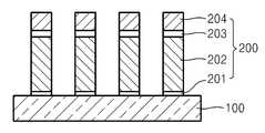
도 1a 내지 도 1c는 본 발명의 실시예에 따른 반도체 소자의 제조 방법을 순서대로 도시하는 단면도이다.1A to 1C are cross-sectional views sequentially illustrating a method of manufacturing a semiconductor device according to an embodiment of the present invention.
도 1a에 도시된 바와 같이, 서로 인접한 복수의 배선들(20)이 형성된 반도체 기판(10)을 준비한다. 배선들(20) 하부의 반도체 기판(10)에는 배선들과 전기적으로 연결되는 다양한 트랜지스터의 소오스/드레인, 캐패시터, 다이오드 및 층간 절연막 등의 다양한 부재들(미도시)이 배치될 수 있다.As shown in FIG. 1A, a
이후, 도 1b에 도시된 바와 같이, 배선들(20)을 전기적으로 고립시키기 위하여, 배선들(20) 사이의 공간에 에어 갭(g)을 가지면서, 상기 공간의 상부(t)를 채우는 절연막(30)을 형성한다. 공간의 상부(t)가 완전히 채워지면, 에어 갭(g)은 폐쇄된다. 절연막(30)은 열 화학기상증착법(thermal chemical vapor deposition; thermal CVD)에 의해 형성된다. 당해 기술 분야에서 잘 알려진 바와 같이, 증착 챔버의 증착 압력 및 증착 온도 등의 증착 변수를 조절하여, 반응 가스의 확산도(diffusivity) 및 절연막의 성막 속도 등을 제어함으로써, 에어 갭(g)을 갖는 절연막(30)을 형성할 수 있다.Then, as shown in FIG. 1B, in order to electrically isolate the
일부 실시예에서, 절연막(30)은 실리콘 산화막으로 이루어질 수 있다. 선택적으로는, 기생 캐패시턴스를 감소시키기 위해 상기 실리콘 산화막보다 유전율이 작은 저유전율 재료로 이루어진 절연막을 형성할 수도 있다. 저유전율 절연막으로서, 실리콘 불화 산화물(SiOF), 실리콘 탄화 산화물(SiOC), 실리콘 붕소화 질화 물(SiBN) 및 실리콘 붕소화 탄화 질화물(SiBCN) 등이 채택될 수 있다.In some embodiments, the
일부 실시예에서, 절연막(30)은 저압 화학기상증착법(LPCVD)에 의해 형성될 수 있다. 이 경우, LPCVD의 증착 압력은 0.3 Torr 내지 10 Torr일 수 있다. 증착 온도는 400 ℃ 내지 600 ℃일 수 있다. 예를 들면, 디에틸실렌(DES)과 같은 실리콘 함유 가스와 O2, O3, NO, N2O 및 H2O 와 같은 산소 함유 가스로 이루어진 혼합 가스를 사용하여, LPCVD 법에 의해 실리콘 산화물로 이루어진 절연막을 형성할 수 있다.In some embodiments,
실리콘 함유 가스의 분압에 대한 산소의 분압비, 즉, PO/PSi가 5 내지 50이 되도록, 산소의 분압을 실리콘에 비해 현저히 증가시켜 에어 갭을 갖는 실리콘 산화막을 형성할 수 있다. LPCVD에서 실리콘 함유 가스의 분압에 대한 산소 가스의 분압이 증가될수록 실리콘 산화막의 단차 피복성은 열화되며, 이에 따라 에어 갭이 용이하게 형성될 수 있다. 이 경우, 증착 온도는 비교적 높은 400 ℃ 내지 600 ℃로 유지하여, DES와 같은 반응 가스로부터 유인된 불순물, 특히 수소가 절연막(30)에 내포되는 것을 감소시킬 수 있다. 상술한 증착 압력, 증착 온도 및 반응 가스는 예시적일 뿐, 본 발명은 이에 한정되지 않으며, 상술한 절연막의 재료에 따라 다르게 선택될 수 있다.The partial pressure of oxygen can be significantly increased compared to that of silicon so that the partial pressure ratio of oxygen to partial pressure of the silicon-containing gas, that is, PO / PSi is 5 to 50, thereby forming a silicon oxide film having an air gap. As the partial pressure of the oxygen gas is increased with respect to the partial pressure of the silicon-containing gas in LPCVD, the step coverage of the silicon oxide film is deteriorated, so that an air gap can be easily formed. In this case, the deposition temperature can be maintained at a relatively high 400 to 600 ℃, it is possible to reduce the inclusion of impurities, especially hydrogen attracted from the reaction gas, such as DES, in the
절연막(30)을 형성한 후, 도 1c에 도시된 바와 같이, 절연막(30)의 상부에 보호막(40)을 더 형성할 수 있다. 보호막(40)은, 절연막(30)의 기계적 및 열적 특성 등을 보강하기 위한 것으로서, PECVD법에 의한 TEOS막, 시록산(siloxanes) 및 규산염(silicate) 등으로 이루이진 SOG(spin on glass)일 수 있다. 일부 실시예에서는 보호막(40)을 형성한 후, 에치백(etchback) 또는 기계화학적식각(CMP) 공정에 의해 보호막(40)을 평탄화하는 공정을 더 수행할 수도 있다.After forming the insulating
본 발명의 실시예에 따른 저압화학기상증착법에 의해 증착된 절연막은, 에어 갭을 형성하기 위하여 당해 기술 분야에서 주로 채택되는 플라즈마강화 화학기상증착법((plasma enhanced chemical vapor deposition; PECVD)에 비하여, 반응 가스로부터 유인되는 수소와 같은 불순물이 절연막 내에 덜 내포될 수 있으며, 이로 인하여, 반도체 소자의 신뢰성에 영향을 주지 않는 우수한 절연막을 제공할 수 있다. 예를 들어, PECVD법에 의한 TEOS(tetraethylortho silicate)막은 비교적 저온, 예를 들면 350 ℃의 증착 온도에서 형성되기 때문에, 절연막 내에 불순물인 수소를 많이 함유한다. 이러한, 수소는 활성 영역 또는 게이트 스택 내부로 확산되어, 반도체 소자의 신뢰성을 저해할 수 있다. 그러나, 열 화학기상증착법은 PECVD법에 비하여 고온에서 절연막을 증착하기 때문에, 수소가 함유된 반응 가스에 의해 절연막을 형성하더라도, 절연막 내부에 수소가 덜 포함되어 반도체 소자의 신뢰성을 확보할 수 있다.The insulating film deposited by the low pressure chemical vapor deposition method according to an embodiment of the present invention, compared to plasma enhanced chemical vapor deposition (PECVD), which is mainly adopted in the art to form an air gap, the reaction Impurities such as hydrogen attracted from the gas may be less contained in the insulating film, thereby providing an excellent insulating film that does not affect the reliability of the semiconductor device, for example, tetraethylortho silicate (TEOS) by PECVD. Since the film is formed at a relatively low temperature, for example, a deposition temperature of 350 ° C., it contains a large amount of hydrogen as an impurity in the insulating film, which can diffuse into the active region or the gate stack, which may impair the reliability of the semiconductor device. However, since the thermal chemical vapor deposition method deposits an insulating film at a high temperature compared with PECVD, hydrogen Even if the insulating film is formed by the reaction gas contained therein, less hydrogen is included in the insulating film to ensure the reliability of the semiconductor device.
도 2a 내지 도 2c는 본 발명의 다른 실시예에 따른 반도체 소자의 제조 방법을 도시하는 단면도이다.2A to 2C are cross-sectional views illustrating a method of manufacturing a semiconductor device in accordance with another embodiment of the present invention.
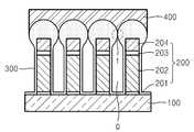
도 2a를 참조하면, 채널 영역을 포함하는 반도체 기판(100)을 준비한다. 이후, 채널 영역 상에 다중막으로 이루어진 복수의 게이트 스택(200)을 형성한다. 로직 소자의 트랜지스터 또는 메모리 소자의 메모리 셀을 구현하기 위하여, 다중막 은 예를 들면, 활성 영역 상에 순차대로 적층된 게이트 절연막 및 게이트 전극(미도시)을 포함할 수 있다. 또는, 플래시 메모리와 같은 비휘발성 메모리 소자를 구현하기 위해, 다중막(200)은 도시된 바와 같이 터널링 산화막(201), 전하저장층(202), 블로킹 절연막(203) 및 제어 게이트 전극(204)을 포함할 수 있다. 전하저장층(202)는 당해 기술 분야에서 잘 알려진 바와 같이, 플로팅 게이트 또는 전하트랩층일 수 있다.Referring to FIG. 2A, a
후속하여, 도 2b에 도시된 바와 같이, 열 화학기상증착법에 의해 게이트 스택(200) 사이의 공간에 에어 갭(g)을 가지면서, 공간의 상부를 채우는 절연막(300)을 형성한다. 절연막(300)은 게이트 스택(200)의 측벽 및 반도체 기판(100)의 노출된 활성 영역 상에 얇게 증착되어, 게이트 스택(200)의 측벽과 활성 영역을 보호하는 스페이서 역할을 할 수 있다.Subsequently, as shown in FIG. 2B, an insulating
상술한 바와 같이 절연막(300)은, 증착 압력 및 온도 등의 증착 변수를 제어함으로써 형성될 수 있다. 일부 실시예에서, 절연막(300)은 저압 화학기상증착법 (LPCVD)에 의해 형성될 수 있다. 예를 들면, 실리콘 함유 가스의 분압에 대한 산소의 분압비, 즉, PO/PSi가 5 내지 50이 되도록, 디에틸실렌(DES)과 같은 실리콘 함유 가스와 O2, O3, NO, N2O 및 H2O 와 같은 산소 함유 가스를 증착 챔버에 각각 공급하고, 0.3 Torr 내지 10 Torr의 증착 압력과 400 ℃ 내지 600 ℃의 증착 온도에서, 에어 갭(g)을 갖는 실리콘 산화막을 형성할 수 있다.As described above, the insulating
일부 실시예에서는, 절연막(300)을 형성한 후, 도 2c에 도시된 바와 같이, 절연막(300)의 상부에 보호막(400)을 더 형성할 수 있다. 보호막(400)은 절연막(300)의 기계적 및 열적 특성 등을 보강하기 위한 것으로서, PECVD법에 의한 TEOS막, 시록산(siloxanes) 및 규산염(silicate) 등으로 이루이진 SOG(spin on glass)일 수 있다. 일부 실시예에서는 보호막(400)을 형성한 후, 에치백(etchback) 또는 기계화학적식각(CMP) 공정에 의해 보호막(400)을 평탄화하는 공정을 더 수행할 수도 있다.In some embodiments, after forming the insulating
본 발명의 열 화학기상증착법에 의해 증착된 절연막은, 플라즈마강화 화학기상증착법((plasma enhanced chemical vapor deposition; PECVD)에 비하여, 반응 가스로부터 유인되는 불순물이 절연막 내에 덜 내포될 수 있으며, 이로 인하여, 반도체 소자의 신뢰성에 영향을 주지 않을 수 있다. 또한, 최근 로직 회로를 비롯한 메모리 소자의 동작 전압이 감소됨에 따라 게이트 절연막 또는 터널링 절연막의 두께가 점차적으로 감소되어, 전기적 에너지에 의해 절연막을 형성하는 PECVD의 경우, 노출된 게이트 스택 내 유전층, 예를 들면, 게이트 절연막 및/또는 터널링 절연막이 쉽게 플라즈마 손상을 입을 수 있다. 그러나, 본 발명의 열 화학기상증착법은 열 에너지에 의해 절연막을 형성하므로, 전기적 에너지에 의해 절연막을 형성하는 PECVD에 비하여, 상기 게이트 절연막 및/또는 터널링 절연막에 손상을 덜 초래할 수 있다.Insulating films deposited by the thermal chemical vapor deposition method of the present invention, as compared with plasma enhanced chemical vapor deposition (PECVD), impurities attracted from the reaction gas may be less contained in the insulating film, thereby, In addition, the thickness of the gate insulating film or the tunneling insulating film is gradually reduced as the operating voltage of the memory device including the logic circuit is recently decreased, thereby forming the insulating film by electrical energy. In this case, the dielectric layer in the exposed gate stack, for example, the gate insulating film and / or the tunneling insulating film, can be easily damaged by plasma, however, the thermal chemical vapor deposition method of the present invention forms an insulating film by thermal energy, so Compared to PECVD which forms an insulating film by energy, the gate insulating film and And / or less damage to the tunneling insulating film.
이상에서 설명한 본 발명이 전술한 실시예 및 첨부된 도면에 한정되지 않으며, 본 발명의 기술적 사상을 벗어나지 않는 범위 내에서 여러가지 치환, 변형 및 변경이 가능하다는 것은, 본 발명이 속하는 기술분야에서 통상의 지식을 가진 자에 게 있어 명백할 것이다.The present invention described above is not limited to the above-described embodiments and the accompanying drawings, and various substitutions, modifications, and alterations are possible within the scope without departing from the technical spirit of the present invention, which are common in the art. It will be clear to those who have knowledge.
도 1a 내지 도 1c는 본 발명의 실시예에 따른 반도체 소자의 제조 방법을 순서대로 도시하는 단면도이다.1A to 1C are cross-sectional views sequentially illustrating a method of manufacturing a semiconductor device according to an embodiment of the present invention.
도 2a 내지 도 2c는 본 발명의 다른 실시예에 따른 반도체 소자의 제조 방법을 도시하는 단면도이다.2A to 2C are cross-sectional views illustrating a method of manufacturing a semiconductor device in accordance with another embodiment of the present invention.
* 도면의 주요부분에 대한 부호의 설명 *Description of the Related Art [0002]
10, 100: 반도체 기판20, 200: 각각 배선과 게이트 스택10, 100:
30, 300: 절연막40, 400: 보호막30, 300: insulating
Claims (19)
Translated fromKoreanPriority Applications (3)
| Application Number | Priority Date | Filing Date | Title |
|---|---|---|---|
| KR1020070078706AKR101356695B1 (en) | 2007-08-06 | 2007-08-06 | Method of fabricating semiconductor device |
| US12/181,166US8129264B2 (en) | 2007-08-06 | 2008-07-28 | Method of fabricating a semiconductor device |
| US13/363,673US8563421B2 (en) | 2007-08-06 | 2012-02-01 | Method of fabricating semiconductor device |
Applications Claiming Priority (1)
| Application Number | Priority Date | Filing Date | Title |
|---|---|---|---|
| KR1020070078706AKR101356695B1 (en) | 2007-08-06 | 2007-08-06 | Method of fabricating semiconductor device |
Publications (2)
| Publication Number | Publication Date |
|---|---|
| KR20090014628A KR20090014628A (en) | 2009-02-11 |
| KR101356695B1true KR101356695B1 (en) | 2014-01-29 |
Family
ID=40346943
Family Applications (1)
| Application Number | Title | Priority Date | Filing Date |
|---|---|---|---|
| KR1020070078706AActiveKR101356695B1 (en) | 2007-08-06 | 2007-08-06 | Method of fabricating semiconductor device |
Country Status (2)
| Country | Link |
|---|---|
| US (2) | US8129264B2 (en) |
| KR (1) | KR101356695B1 (en) |
Families Citing this family (34)
| Publication number | Priority date | Publication date | Assignee | Title |
|---|---|---|---|---|
| US7724005B1 (en)* | 2007-07-24 | 2010-05-25 | Clemson University | High-frequency structures for nanoelectronics and molecular electronics |
| JP2011061085A (en)* | 2009-09-11 | 2011-03-24 | Toshiba Corp | Ferroelectric storage device |
| JP5882583B2 (en)* | 2010-02-04 | 2016-03-09 | 東京応化工業株式会社 | Silica-based film forming material for air gap formation and air gap forming method |
| US8546239B2 (en) | 2010-06-11 | 2013-10-01 | Sandisk Technologies Inc. | Methods of fabricating non-volatile memory with air gaps |
| US8603890B2 (en) | 2010-06-19 | 2013-12-10 | Sandisk Technologies Inc. | Air gap isolation in non-volatile memory |
| US8946048B2 (en) | 2010-06-19 | 2015-02-03 | Sandisk Technologies Inc. | Method of fabricating non-volatile memory with flat cell structures and air gap isolation |
| US8492224B2 (en)* | 2010-06-20 | 2013-07-23 | Sandisk Technologies Inc. | Metal control gate structures and air gap isolation in non-volatile memory |
| JP2012109450A (en)* | 2010-11-18 | 2012-06-07 | Toshiba Corp | Nonvolatile semiconductor memory device and manufacturing method thereof |
| US8778749B2 (en) | 2011-01-12 | 2014-07-15 | Sandisk Technologies Inc. | Air isolation in high density non-volatile memory |
| JP5395828B2 (en)* | 2011-02-25 | 2014-01-22 | 株式会社東芝 | Nonvolatile semiconductor memory device and manufacturing method thereof |
| US8643123B2 (en)* | 2011-04-13 | 2014-02-04 | Freescale Semiconductor, Inc. | Method of making a semiconductor structure useful in making a split gate non-volatile memory cell |
| KR101813513B1 (en) | 2011-11-30 | 2018-01-02 | 삼성전자주식회사 | Semiconductor devices and methods of manufacturing semiconductor devices |
| US9123714B2 (en)* | 2012-02-16 | 2015-09-01 | Sandisk Technologies Inc. | Metal layer air gap formation |
| KR101917815B1 (en)* | 2012-05-31 | 2018-11-13 | 에스케이하이닉스 주식회사 | Semiconductor device with air gap and method for fabricating the same |
| US8652962B2 (en) | 2012-06-19 | 2014-02-18 | Taiwan Semiconductor Manufacturing Co., Ltd. | Etch damage and ESL free dual damascene metal interconnect |
| TWI464831B (en) | 2012-06-27 | 2014-12-11 | Powerchip Technology Corp | Method of fabricating non-volatile memory device |
| US9123577B2 (en) | 2012-12-12 | 2015-09-01 | Sandisk Technologies Inc. | Air gap isolation in non-volatile memory using sacrificial films |
| KR102001493B1 (en)* | 2013-04-16 | 2019-07-18 | 에스케이하이닉스 주식회사 | Semiconductor device with air gap and method for fabricating the same |
| US9153455B2 (en)* | 2013-06-19 | 2015-10-06 | Micron Technology, Inc. | Methods of forming semiconductor device structures, memory cells, and arrays |
| US9349740B2 (en) | 2014-01-24 | 2016-05-24 | Sandisk Technologies Inc. | Non-volatile storage element with suspended charge storage region |
| US9177853B1 (en) | 2014-05-14 | 2015-11-03 | Sandisk Technologies Inc. | Barrier layer stack for bit line air gap formation |
| US9478461B2 (en) | 2014-09-24 | 2016-10-25 | Sandisk Technologies Llc | Conductive line structure with openings |
| US9524904B2 (en) | 2014-10-21 | 2016-12-20 | Sandisk Technologies Llc | Early bit line air gap formation |
| US9401305B2 (en) | 2014-11-05 | 2016-07-26 | Sandisk Technologies Llc | Air gaps structures for damascene metal patterning |
| US9847249B2 (en) | 2014-11-05 | 2017-12-19 | Sandisk Technologies Llc | Buried etch stop layer for damascene bit line formation |
| US9524973B1 (en) | 2015-06-30 | 2016-12-20 | Sandisk Technologies Llc | Shallow trench air gaps and their formation |
| US9524974B1 (en) | 2015-07-22 | 2016-12-20 | Sandisk Technologies Llc | Alternating sidewall assisted patterning |
| US9391081B1 (en) | 2015-09-08 | 2016-07-12 | Sandisk Technologies Llc | Metal indentation to increase inter-metal breakdown voltage |
| US9607997B1 (en) | 2015-09-08 | 2017-03-28 | Sandisk Technologies Inc. | Metal line with increased inter-metal breakdown voltage |
| KR102658192B1 (en)* | 2016-07-27 | 2024-04-18 | 삼성전자주식회사 | Semiconductor devices and methods of manufacturing semiconductor devices |
| WO2018125124A1 (en)* | 2016-12-29 | 2018-07-05 | Intel Corporation | Creating dielectric helmet films using pulsed gas deposition |
| US10665499B2 (en)* | 2018-06-28 | 2020-05-26 | Intel Corporation | Integrated circuit with airgaps to control capacitance |
| TWI733412B (en) | 2020-04-13 | 2021-07-11 | 華邦電子股份有限公司 | Semiconductor device with air gap and method of fabricating the same |
| CN113555365B (en)* | 2020-04-24 | 2023-10-17 | 华邦电子股份有限公司 | Semiconductor device with air gap and method of manufacturing the same |
Citations (4)
| Publication number | Priority date | Publication date | Assignee | Title |
|---|---|---|---|---|
| KR20010011638A (en)* | 1999-07-29 | 2001-02-15 | 김영환 | Structure of semiconductor device and method of manufacturing the same |
| JP2006302950A (en)* | 2005-04-15 | 2006-11-02 | Renesas Technology Corp | Nonvolatile semiconductor device and method of manufacturing nonvolatile semiconductor device |
| KR20070046412A (en)* | 2005-10-31 | 2007-05-03 | 삼성전자주식회사 | Nonvolatile Memory Device and Manufacturing Method Thereof |
| KR20080022380A (en)* | 2006-09-06 | 2008-03-11 | 주식회사 하이닉스반도체 | Manufacturing method of semiconductor device |
Family Cites Families (8)
| Publication number | Priority date | Publication date | Assignee | Title |
|---|---|---|---|---|
| US5869379A (en)* | 1997-12-08 | 1999-02-09 | Advanced Micro Devices, Inc. | Method of forming air gap spacer for high performance MOSFETS' |
| JP2000031278A (en) | 1998-07-10 | 2000-01-28 | Nippon Steel Corp | Method for manufacturing semiconductor device |
| KR100286126B1 (en) | 1999-02-13 | 2001-03-15 | 윤종용 | Process for forming air gaps using a multilayer passivation in a dielectric between interconnections |
| KR20010003458A (en) | 1999-06-23 | 2001-01-15 | 김영환 | Method of forming wiring for semiconductor device |
| US20050181633A1 (en)* | 2004-02-17 | 2005-08-18 | Hochberg Arthur K. | Precursors for depositing silicon-containing films and processes thereof |
| JP4679193B2 (en)* | 2005-03-22 | 2011-04-27 | 株式会社東芝 | Semiconductor device manufacturing method and semiconductor device |
| US20060216929A1 (en)* | 2005-03-28 | 2006-09-28 | Hyun-Mog Park | Etch stopless dual damascene structure and method of fabrication |
| KR100770700B1 (en)* | 2006-11-06 | 2007-10-30 | 삼성전자주식회사 | Nonvolatile Memory Device and Manufacturing Method Thereof |
- 2007
- 2007-08-06KRKR1020070078706Apatent/KR101356695B1/enactiveActive
- 2008
- 2008-07-28USUS12/181,166patent/US8129264B2/enactiveActive
- 2012
- 2012-02-01USUS13/363,673patent/US8563421B2/enactiveActive
Patent Citations (4)
| Publication number | Priority date | Publication date | Assignee | Title |
|---|---|---|---|---|
| KR20010011638A (en)* | 1999-07-29 | 2001-02-15 | 김영환 | Structure of semiconductor device and method of manufacturing the same |
| JP2006302950A (en)* | 2005-04-15 | 2006-11-02 | Renesas Technology Corp | Nonvolatile semiconductor device and method of manufacturing nonvolatile semiconductor device |
| KR20070046412A (en)* | 2005-10-31 | 2007-05-03 | 삼성전자주식회사 | Nonvolatile Memory Device and Manufacturing Method Thereof |
| KR20080022380A (en)* | 2006-09-06 | 2008-03-11 | 주식회사 하이닉스반도체 | Manufacturing method of semiconductor device |
Also Published As
| Publication number | Publication date |
|---|---|
| KR20090014628A (en) | 2009-02-11 |
| US20120129356A1 (en) | 2012-05-24 |
| US20090042383A1 (en) | 2009-02-12 |
| US8563421B2 (en) | 2013-10-22 |
| US8129264B2 (en) | 2012-03-06 |
Similar Documents
| Publication | Publication Date | Title |
|---|---|---|
| KR101356695B1 (en) | Method of fabricating semiconductor device | |
| CN101647105B (en) | Method for manufacturing semiconductor device | |
| CN100353542C (en) | Integrated circuit and its forming method and electronic component | |
| US11574871B2 (en) | Semiconductor device | |
| US20070246831A1 (en) | Method for manufacturing a layer arrangement and layer arrangement | |
| US8372732B2 (en) | Method for fabricating non-volatile memory device | |
| KR101674057B1 (en) | Semiconductor chip structure having a complex reinforced insulator and method of fabricating the same | |
| US7790601B1 (en) | Forming interconnects with air gaps | |
| CN100517640C (en) | Manufacturing method of semiconductor device and semiconductor device | |
| CN111180320B (en) | Manufacturing method of grid electrode, structure thereof and semiconductor device | |
| CN105336680A (en) | Semiconductor device, manufacturing method thereof and electronic device | |
| CN100375248C (en) | Heterogeneous low dielectric constant material and method for forming the same | |
| US7351653B2 (en) | Method for damascene process | |
| US6277732B1 (en) | Method of planarizing inter-metal dielectric layer | |
| KR100905828B1 (en) | Metal wiring of semiconductor device and method of forming the same | |
| US6806208B2 (en) | Semiconductor device structured to prevent oxide damage during HDP CVD | |
| US7250364B2 (en) | Semiconductor devices with composite etch stop layers and methods of fabrication thereof | |
| US6835648B2 (en) | Semiconductor PMD layer dielectric | |
| KR100694982B1 (en) | Method for forming passivation layer of semiconductor device | |
| KR100401504B1 (en) | Method of forming a passivation layer in a semiconductor device | |
| JP2001093979A (en) | Semiconductor device and manufacturing method thereof | |
| KR20080098681A (en) | How to reduce interconnect line-to-line capacitance using low-k spacers | |
| KR100459063B1 (en) | Method for manufacturing intermetal dielectric layer of semiconductor device | |
| KR100590397B1 (en) | Method for forming passivation layer of semiconductor device | |
| CN114823499A (en) | Semiconductor device with a plurality of semiconductor chips |
Legal Events
| Date | Code | Title | Description |
|---|---|---|---|
| PA0109 | Patent application | Patent event code:PA01091R01D Comment text:Patent Application Patent event date:20070806 | |
| PG1501 | Laying open of application | ||
| A201 | Request for examination | ||
| PA0201 | Request for examination | Patent event code:PA02012R01D Patent event date:20120502 Comment text:Request for Examination of Application Patent event code:PA02011R01I Patent event date:20070806 Comment text:Patent Application | |
| E902 | Notification of reason for refusal | ||
| PE0902 | Notice of grounds for rejection | Comment text:Notification of reason for refusal Patent event date:20130624 Patent event code:PE09021S01D | |
| E701 | Decision to grant or registration of patent right | ||
| PE0701 | Decision of registration | Patent event code:PE07011S01D Comment text:Decision to Grant Registration Patent event date:20131125 | |
| GRNT | Written decision to grant | ||
| PR0701 | Registration of establishment | Comment text:Registration of Establishment Patent event date:20140122 Patent event code:PR07011E01D | |
| PR1002 | Payment of registration fee | Payment date:20140123 End annual number:3 Start annual number:1 | |
| PG1601 | Publication of registration | ||
| FPAY | Annual fee payment | Payment date:20170102 Year of fee payment:4 | |
| PR1001 | Payment of annual fee | Payment date:20170102 Start annual number:4 End annual number:4 | |
| FPAY | Annual fee payment | Payment date:20191226 Year of fee payment:7 | |
| PR1001 | Payment of annual fee | Payment date:20191226 Start annual number:7 End annual number:7 | |
| PR1001 | Payment of annual fee | Payment date:20201230 Start annual number:8 End annual number:8 | |
| PR1001 | Payment of annual fee | Payment date:20211229 Start annual number:9 End annual number:9 | |
| PR1001 | Payment of annual fee | Payment date:20221221 Start annual number:10 End annual number:10 | |
| PR1001 | Payment of annual fee | Payment date:20231226 Start annual number:11 End annual number:11 |