KR101354750B1 - Semiconductor Device And Fabricating Method Thereof - Google Patents
Semiconductor Device And Fabricating Method ThereofDownload PDFInfo
- Publication number
- KR101354750B1 KR101354750B1KR1020120041674AKR20120041674AKR101354750B1KR 101354750 B1KR101354750 B1KR 101354750B1KR 1020120041674 AKR1020120041674 AKR 1020120041674AKR 20120041674 AKR20120041674 AKR 20120041674AKR 101354750 B1KR101354750 B1KR 101354750B1
- Authority
- KR
- South Korea
- Prior art keywords
- substrate
- coupling portion
- semiconductor die
- bond
- solder bump
- Prior art date
- Legal status (The legal status is an assumption and is not a legal conclusion. Google has not performed a legal analysis and makes no representation as to the accuracy of the status listed.)
- Active
Links
Images


Classifications
- H—ELECTRICITY
- H01—ELECTRIC ELEMENTS
- H01L—SEMICONDUCTOR DEVICES NOT COVERED BY CLASS H10
- H01L2224/00—Indexing scheme for arrangements for connecting or disconnecting semiconductor or solid-state bodies and methods related thereto as covered by H01L24/00
- H01L2224/01—Means for bonding being attached to, or being formed on, the surface to be connected, e.g. chip-to-package, die-attach, "first-level" interconnects; Manufacturing methods related thereto
- H01L2224/10—Bump connectors; Manufacturing methods related thereto
- H01L2224/15—Structure, shape, material or disposition of the bump connectors after the connecting process
- H01L2224/16—Structure, shape, material or disposition of the bump connectors after the connecting process of an individual bump connector
- H01L2224/161—Disposition
- H01L2224/16151—Disposition the bump connector connecting between a semiconductor or solid-state body and an item not being a semiconductor or solid-state body, e.g. chip-to-substrate, chip-to-passive
- H01L2224/16221—Disposition the bump connector connecting between a semiconductor or solid-state body and an item not being a semiconductor or solid-state body, e.g. chip-to-substrate, chip-to-passive the body and the item being stacked
- H01L2224/16225—Disposition the bump connector connecting between a semiconductor or solid-state body and an item not being a semiconductor or solid-state body, e.g. chip-to-substrate, chip-to-passive the body and the item being stacked the item being non-metallic, e.g. insulating substrate with or without metallisation
- H—ELECTRICITY
- H01—ELECTRIC ELEMENTS
- H01L—SEMICONDUCTOR DEVICES NOT COVERED BY CLASS H10
- H01L2924/00—Indexing scheme for arrangements or methods for connecting or disconnecting semiconductor or solid-state bodies as covered by H01L24/00
- H01L2924/15—Details of package parts other than the semiconductor or other solid state devices to be connected
- H01L2924/151—Die mounting substrate
- H01L2924/153—Connection portion
- H01L2924/1531—Connection portion the connection portion being formed only on the surface of the substrate opposite to the die mounting surface
- H01L2924/15311—Connection portion the connection portion being formed only on the surface of the substrate opposite to the die mounting surface being a ball array, e.g. BGA
Landscapes
- Wire Bonding (AREA)
Abstract
Translated fromKoreanDescription
Translated fromKorean본 발명은 반도체 디바이스 및 그 제조 방법에 관한 것이다.
The present invention relates to a semiconductor device and a method of manufacturing the same.
현재 전자 산업의 추세에서는 더욱 경량화, 소형화, 고속화, 다기능화, 고성능화되고 높은 신뢰성을 갖는 제품들이 요구되고 있다. 이와 같은 제품 설계를 가능하게 하는 중요한 기술 중 하나가 반도체 디바이스의 제조 기술이며, 이에 따라 반도체 디바이스 산업 역시 발전하고 있다. 반도체 디바이스 역시 다양한 요구에 부합하기 위해 점차 반도체 디바이스의 크기를 줄이기 위한 개발이 이루어져 왔다.Current trends in the electronics industry require products that are lighter, smaller, faster, more versatile, higher in performance and more reliable. One of the important technologies enabling such a product design is the manufacturing technology of semiconductor devices, and accordingly, the semiconductor device industry is also developing. Semiconductor devices have also been developed to reduce the size of semiconductor devices gradually to meet various needs.
그리고 최근의 반도체 다이 중 일부는 기존의 도전성 와이어 대신 솔더 범프를 이용하여 서브스트레이트의 상부에 바로 반도체 다이를 플립칩(flip chip)의 형태로 결합하는 방식을 사용하는 방법을 채택하고 있다. 그런데, 이러한 반도체 디바이스에서는 솔더 범프를 통해 서브스트레이트와 반도체 다이가 신호를 입출력하기 때문에, 이들을 안정적으로 결합시키는 것이 신뢰성 확보에서 중요하다.
Some of the recent semiconductor dies adopt a method of directly bonding a semiconductor die in the form of a flip chip on top of the substrate using solder bumps instead of the conventional conductive wires. However, in such a semiconductor device, since the substrate and the semiconductor die input and output signals through solder bumps, it is important to securely combine them.
본 발명은 반도체 다이를 서브스트레이트와 연결하는 솔더 범프의 파손을 방지하여 신뢰성을 확보할 수 있는 반도체 디바이스를 제공한다.
The present invention provides a semiconductor device capable of ensuring reliability by preventing breakage of solder bumps connecting the semiconductor die to the substrate.
본 발명에 따른 반도체 디바이스는 일면에 복수개의 도전성 패드가 형성된 서브스트레이트; 상기 서브스트레이트의 일면에 결합되고, 복수개의 본드 패드를 갖는 반도체 다이; 및 상기 서브스트레이트의 도전성 패드 및 상기 본드 패드의 사이에 형성된 적어도 하나의 솔더 범프를 포함하고, 상기 서브스트레이트의 도전성 패드 또는 상기 반도체 다이의 본드 패드 중에서 적어도 하나는 상기 솔더 범프와 접하는 영역에 금속으로 형성된 결합부를 가질 수 있다.A semiconductor device according to the present invention includes a substrate having a plurality of conductive pads formed on one surface thereof; A semiconductor die coupled to one surface of the substrate and having a plurality of bond pads; And at least one solder bump formed between the conductive pad of the substrate and the bond pad, wherein at least one of the conductive pad of the substrate or the bond pad of the semiconductor die is formed of a metal in an area in contact with the solder bump. It may have a coupling portion formed.
여기서, 상기 결합부는 상기 서브스트레이트의 도전성 패드 또는 상기 반도체 다이의 본드 패드 중 적어도 하나가 상기 솔더 범프와 접하는 영역 중 일부에만 형성될 수 있다.Here, the coupling part may be formed only in a part of the region where at least one of the conductive pad of the substrate or the bond pad of the semiconductor die contacts the solder bump.
그리고 상기 결합부는 상기 서브스트레이트의 도전성 패드 또는 상기 반도체 다이의 본드 패드 중 적어도 하나가 상기 솔더 범프와 접하는 영역의 가장자리를 따라 형성될 수 있다.The coupling portion may be formed along an edge of an area where at least one of the conductive pad of the substrate or the bond pad of the semiconductor die contacts the solder bump.
또한, 상기 결합부는 상기 솔더 범프와 금속간 결합을 형성할 수 있다.In addition, the coupling portion may form a bond between the solder bump and the metal.
또한, 상기 결합부는 상기 결합부로부터 상기 솔더 범프를 향하는 방향으로 금속간 결합을 형성할 수 있다.In addition, the coupling part may form an intermetallic coupling in a direction from the coupling part toward the solder bumps.
또한, 상기 결합부는 상기 솔더 범프의 주석(Sn) 성분과 금속간 결합을 형성할 수 있다.In addition, the coupling part may form an intermetallic bond with a tin (Sn) component of the solder bump.
또한, 상기 결합부는 구리(Cu)를 포함하는 재질로 구성될 수 있다.In addition, the coupling part may be made of a material including copper (Cu).
또한, 상기 서브스트레이트는 상기 도전성 패드와 상기 결합부의 사이에 확산 방지층을 더 포함할 수 있다.In addition, the substrate may further include a diffusion barrier layer between the conductive pad and the coupling portion.
또한, 상기 확산 방지층은 니켈(Ni)을 포함하여 구성될 수 있다.In addition, the diffusion barrier layer may include nickel (Ni).
또한, 상기 반도체 다이는 상기 본드 패드와 상기 결합부의 사이에 UBM(Under Bump Metal)을 더 포함할 수 있다.The semiconductor die may further include an under bump metal (UBM) between the bond pad and the coupling portion.
또한, 상기 UBM의 상기 결합부와 결합되는 최외곽층은 니켈(Ni)을 포함하는 재질로 구성될 수 있다.
In addition, the outermost layer coupled with the coupling portion of the UBM may be made of a material containing nickel (Ni).
본 발명에 따른 반도체 디바이스는 반도체 다이의 UBM의 일부 영역에 결합부를 형성하거나, 또는 서브스트레이트의 도전성 패드에 위치한 확산 방지층의 일부 영역에 결합부를 형성하여, 솔더 범프와 금속간 결합을 형성하도록 함으로써, 솔더 범프의 주석(Sn) 손실은 줄이면서도 반도체 다이와 솔더 범프 사이의 결합력이 높아지도록 하여 신뢰성을 확보할 수 있다.
The semiconductor device according to the present invention forms a bond in a portion of the UBM of the semiconductor die, or forms a bond in a portion of the diffusion barrier layer located on the conductive pad of the substrate, thereby forming a solder bump and an intermetallic bond. Tin (Sn) losses in the solder bumps can be reduced, while increasing the bond between the semiconductor die and the solder bumps to ensure reliability.
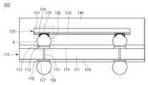
도 1은 본 발명의 일 실시예에 따른 반도체 디바이스의 단면도이다.
도 2는 도 1의 A 부분 확대도이다.
도 3은 도 2의 B 부분 확대도이다.
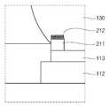
도 4는 본 발명의 다른 실시예에 따른 반도체 디바이스의 단면도이다.
도 5는 도 4의 C 부분 확대도이다.1 is a cross-sectional view of a semiconductor device according to an embodiment of the present invention.
FIG. 2 is an enlarged view of a portion A of FIG. 1.
3 is an enlarged view of a portion B of FIG. 2.
4 is a cross-sectional view of a semiconductor device according to another embodiment of the present invention.
5 is an enlarged view of a portion C of FIG. 4.
본 발명이 속하는 기술분야에 있어서 통상의 지식을 가진 자가 용이하게 실시할 수 있을 정도로 본 발명의 바람직한 실시예를 도면을 참조하여 상세하게 설명하면 다음과 같다.
DETAILED DESCRIPTION OF THE PREFERRED EMBODIMENTS Hereinafter, preferred embodiments of the present invention will be described in detail with reference to the accompanying drawings, so that those skilled in the art can easily carry out the present invention.
도 1은 본 발명의 일 실시예에 따른 반도체 디바이스의 단면도이다. 도 2는 도 1의 A 부분 확대도이다. 도 3은 도 2의 B 부분 확대도이다.1 is a cross-sectional view of a semiconductor device according to an embodiment of the present invention. FIG. 2 is an enlarged view of a portion A of FIG. 1. 3 is an enlarged view of a portion B of FIG. 2.
도 1 내지 도 3을 참조하면, 본 발명의 일 실시예에 따른 반도체 디바이스(100)는 서브스트레이트(110), 반도체 다이(120), 솔더 범프(130), 인캡슐런트(140)를 포함할 수 있다. 또한, 본 발명의 일 실시예에 따른 반도체 디바이스(100)는 서브스트레이트(110)의 하부에 솔더볼(150)을 더 포함할 수 있다.
1 to 3, a
상기 서브스트레이트(110)는 대략 플레이트 형상의 기본층(111)을 기준으로 제 1 면에 형성된 복수의 도전성 패턴(112), 상기 도전성 패턴의 상부에 형성된 제 1 확산 방지층(113), 상기 서브스트레이트(110)의 제 1 면에 형성되어 상기 확산 방지층(113)의 가장자리를 감싸는 제 1 패시베이션층(114), 상기 도전성 패턴(112)에 연결되어 상기 기판(110)을 관통하는 복수의 도전성 비아(115), 상기 기판(110)의 제 1 면에 대해 반대면인 제 2 면에 형성되고 상기 도전성 비아(115)를 통해 상기 도전성 패턴(112)과 연결되는 복수의 랜드(116), 상기 랜드(116)의 하부에 형성된 제 2 확산 방지층(117), 상기 서브스트레이트(110)의 제 2 면에 형성되어 상기 제 2 확산 방지층(117)의 가장자리를 감싸는 제 2 패시베이션층(118)을 포함한다.The
상기 기본층(111)은 전기적으로 절연성이 좋은 재질로 형성된다. 상기 도전성 패턴(112) 및 랜드(116)는 도전성이 우수한 구리(Cu)로 형성되며, 상기 도전성 비아(115)는 상기 기본층(111)을 관통한 비아의 내부를 구리를 충진하여 형성된다. 상기 제 1 확산 방지층(113) 및 제 2 확산 방지층(117)은 상기 도전성 패턴(112) 및 랜드(116)에 형성되며, 니켈(Ni) 또는 금(Au)을 이용하여 형성된다. 상기 확산 방지층(113, 114)은 상기 도전성 패턴(112) 및 랜드(116)를 형성하는 구리가 솔더 범프를 향해 확산되는 것을 방지한다.The
상기 제 1 확산 방지층(113)은 상기 도전성 패턴(112)을 형성하는 구리가 상기 솔더 범프(130)을 형성하는 솔더와 금속간 결합(IMC)을 형성하는 것을 방지한다. 보다 상세히 설명하면, 일반적으로 반도체 디바이스의 제조 공정 이후 습도 테스트(Moisture Resistance Rest, MRT) 또는 열 사이클(Thermal Cycle, TC) 테스트를 수행하게 된다. 그런데 이러한 테스트 공정에서, 상기 솔더 범프(130)의 솔더를 구성하는 주석(Sn) 성분은 상기 도전성 패턴(112)의 구리(Cu)와 금속간 결합(Intermetallic Compound, IMC), 보다 구체적으로는 Cu6Sn5을 형성하기 쉽다. 그리고 이러한 결합 과정에서 상기 솔더 범프(130)에서 주석(Sn) 성분의 소모가 수반되어, 상기 솔더 범프(130)의 내부에서 기공(void)이 발생할 염려가 있다. 또한, 이러한 기공은 솔더 범프(130)의 크랙(crack)을 유발하여, 서브스트레이트(110)와 반도체 다이(120)의 사이에서 결합이 안정적으로 이루어질 수 없도록 하여 신뢰성을 떨어뜨릴 수 있다. 한편, 상기 제 1 확산 방지층(113)은 상기 서브스트레이트(110)의 도전성 패드(112)을 형성하는 구리가 상기 솔더 범프(130)의 내부로 확산되는 것을 방지하여, 상기 금속간 결합을 방지한다. 따라서, 상기 솔더 범프(130)는 상기 습도 테스트(MRT) 또는 열 사이클(TC) 테스트 공정에서 소모되지 않으므로, 상기 솔더 범프(130)의 신뢰성을 높일 수 있다.The first
상기 제 2 확산 방지층(117)은 상기 제 1 확산 방지층(113)과 유사하게 상기 서브스트레이트(110)의 랜드(116)의 하부에 형성될 수 있다. 상기 제 2 확산 방지층(117) 또한 상기 랜드(116)를 구성하는 구리가 상기 솔더볼(150)로 확산되는 것을 방지하여 솔더볼(150)의 주석(Sn)이 금속간 결합을 형성하지 못하도록 함으로써, 주석(Sn)의 손실을 방지할 수 있다.
The second
상기 반도체 다이(120)는 상기 서브스트레이트(110)의 제 1 면에 결합된다. 상기 반도체 다이(120)는 기본층(121)을 기준으로 제 1 면에 복수개의 본드 패드(122)가 형성된다. 또한, 상기 반도체 다이(120)의 제 1 면에는 패시베이션층(123)이 형성되어 상기 본드 패드(122)의 가장자리 상부를 감싼다. 상기 패시베이션층(123)은 제 1 패시베이션층(123a) 및 제 2 패시베이션층(123b)을 포함하여 구성될 수 있다.The semiconductor die 120 is coupled to the first side of the
또한, 상기 본드 패드(122)에는 UBM(Under Bump Metal, 124)이 더 형성되며, 상기 UBM(124)은 솔더 범프(130)를 통해 상기 서브스트레이트(110)의 제 1 확산 방지층(113)과 결합된다.In addition, an under bump metal (UBM) 124 may be further formed on the
여기서, 상기 UBM(124)은 상기 본드 패드(122)와 상기 솔더 범프(130)의 결합력을 높이기 위해 구성된다. 상기 UBM(124)은 상기 순차적으로 구리(Cu)로 형성된 제 1 층(124a), 니켈(Ni)로 형성된 제 2 층(124b), 텅스텐(W)으로 구성된 제 3 층(124c)을 포함하여 구성될 수 있다. 상기 제 1 층(124a)은 알루미늄(Al)으로 구성된 상기 본드 패드(122)의 면적을 확보하고 전기 전도도를 높인다. 상기 제 2층(124b)은 상기 제 1 층(124a)의 구리가 상기 솔더 범프(130)에 확산되는 것을 방지한다. 또한, 상기 제 3 층(124c)은 상기 솔더 범프(130)와 결합력을 높여서 신뢰성을 확보할 수 있다.Here, the UBM 124 is configured to increase the bonding force of the
또한, 상기 반도체 다이(120)는 상기 UBM(124)이 상기 솔더 범프(130)와 접하는 영역 중에서 일 영역에 형성된 결합부(125)를 더 포함한다. 상기 결합부(125)는 구리(Cu) 재질로 형성되어, 상기 솔더 범프(130)와 금속간 결합(126, Cu6Sn5)을 형성할 수 있다. 이 때, 상기 금속간 결합(126)은 상기 결합부(125)로부터 상기 솔더 범프(130)를 향하는 방향으로 형성되며, 상기 결합부(125)는 상기 금속간 결합(126)을 통해 상기 솔더 범프(130)와 안정적으로 결합된다. 또한, 상기 결합부(125)는 상기 UBM(124)의 일부 영역에만 형성되어 있기 때문에, 상기 솔더 범프(130)에서 주석(Sn) 성분이 손실되는 것은 상대적으로 작다. 또한, 상기 UBM(124)이 상기 솔더 범프(130)와 결합되는 영역 중, 상기 UBM(124)의 가장자리 영역이 가장 스트레스를 많이 받는 부위이기 때문에, 상기 결합부(125)는 상기 UBM(124)의 가장자리를 따라 형성될 수 있다. 물론, 상기 결합부(125)가 상기 가장자리 중 일부에만 형성되는 것도 가능하다. 따라서, 본 발명의 일 실시예에 따른 반도체 디바이스(100)는 상기 결합부(125)를 상기 UBM(124)의 적어도 일 영역에 형성함으로써, 솔더 범프(130)의 주석(Sn)이 손실되는 것을 방지하면서도, 반도체 다이(120)와 솔더 범프(130) 사이의 결합력을 높여서 신뢰성을 확보할 수 있다.
In addition, the semiconductor die 120 further includes a
상기 솔더 범프(130)는 상기 서브스트레이트(110)와 반도체 다이(120)의 사이에 형성된다. 상기 솔더 범프(130)는 상기 서브스트레이트(110)의 제 1 확산 방지층(113)과 상기 반도체 다이(120)의 UBM(124)의 사이에 위치한다. 상기 솔더 범프(130)는 상기 반도체 다이(120)의 UBM(124)을 따라 접하도록 형성되며, 특히 상기 결합부(125)를 감싸도록 결합된다. 상기 솔더 범프(130)는 주석(Sn)을 포함하는 재질로서 형성된다. 일 예로, 상기 솔더 범프(130)는 주석(Sn), 납(Pb),은(Ag) 또는 구리(Cu) 등의 합금을 통해 형성될 수 있으나, 상기 솔더 범프(130)의 재질을 한정하는 것은 아니다. 또한, 상술한 것처럼, 상기 솔더 범프(130)의 주석(Sn) 성분은 상기 반도체 다이(120)의 결합부(125)를 구성하는 구리(Cu) 성분과 금속간 결합(126, Cu6Sn5)을 형성한다. 따라서, 상기 솔더 범프(130)는 상기 금속간 결합(126)을 통해 상기 반도체 다이(120)와 안정적으로 결합될 수 있다.
The solder bumps 130 are formed between the
상기 인캡슐런트(140)는 상기 기판(110)의 제 1 면에 형성된다. 상기 인캡슐런트(140)는 내부에 상기 반도체 다이(120) 및 솔더 범프(130)를 감싸도록 형성된다. 상기 인캡슐런트(150)는 상기 반도체 다이(120) 및 솔더 범프(130)를 외부 스트레스로부터 보호한다.
The
상기 솔더볼(150)은 상기 기판(110)의 제 2 면에 형성될 수 있다. 상기 솔더볼(150)은 상기 기판(110)의 랜드(116)에 연결될 수 있으며, 이 경우 통상의 BGA(Ball Grid Array) 구조를 형성할 수 있다. 상기 솔더볼(150)은 주석(Sn), 납(Pb), 은(Ag) 또는 구리(Cu) 등의 합금을 통해 형성될 수 있으나, 상기 솔더볼(150)의 재질을 한정하는 것은 아니다. 또한, 상기 솔더볼(150)이 구비되지 않는 경우, 상기 기판(110)의 랜드(116)가 제 2 면을 통해 노출되어 LGA(Land Grid Array) 구조를 형성하는 것도 가능하다.
The
상기와 같이 하여, 본 발명의 일 실시예에 따른 반도체 디바이스(100)는 반도체 다이(120)의 UBM(124)의 일부 영역에 결합부(125)를 형성하여, 솔더 범프(130)와 금속간 결합을 형성하도록 함으로써, 솔더 범프(130)의 주석(Sn) 손실은 줄이면서도 반도체 다이(120)와 솔더 범프(130) 사이의 결합력이 높아지도록 하여 신뢰성을 확보할 수 있다.
As described above, in the
이하에서는 본 발명의 다른 실시예에 따른 반도체 디바이스의 구성을 설명하도록 한다.Hereinafter, a configuration of a semiconductor device according to another embodiment of the present invention will be described.
도 4는 본 발명의 다른 실시예에 따른 반도체 디바이스의 단면도이다. 도 5는 도 4의 C 부분 확대도이다. 앞서 설명한 실시예와 동일한 구성 및 동작을 갖는 부분에 대해서는 동일한 도면부호를 붙였으며, 이하에서는 앞선 실시예와의 차이점을 위주로 설명하도록 한다.4 is a cross-sectional view of a semiconductor device according to another embodiment of the present invention. 5 is an enlarged view of a portion C of FIG. 4. Portions having the same configuration and operation as those of the above-described embodiment are denoted by the same reference numerals, and differences from the foregoing embodiment will be mainly described below.
도 4 및 도 5를 참조하면, 본 발명의 다른 실시예에 따른 반도체 디바이스(200)는 서브스트레이트(210), 반도체 다이(220), 솔더 범프(130), 인캡슐런트(140)를 포함할 수 있다. 또한, 본 발명의 일 실시예에 따른 반도체 디바이스(100)는 서브스트레이트(110)의 하부에 솔더볼(150)을 더 포함할 수 있다.4 and 5, a
상기 서브스트레이트(210)는 앞선 실시예와 마찬가지로 기본층(111), 도전성 패턴(112), 제 1 확산 방지층(113), 제 1 패시베이션층(114), 도전성 비아(115), 복수의 랜드(116), 제 2 확산 방지층(117), 제 2 패시베이션층(118)을 포함할 수 있다.The
한편, 상기 서브스트레이트(210)는 상기 제 1 확산 방지층(113)의 상부에 형성된 결합부(211)를 포함한다. 상기 결합부(211)는 상기 제 1 확산 방지층(113)의 적어도 일 영역에 형성된다. 또한, 상기 결합부(211)는 상기 제 1 확산 방지층(113)의 가장자리를 따라 형성될 수 있다. 상기 결합부(211)는 구리(Cu) 재질로형성되어, 상기 솔더볼(150)의 주석(Sn) 성분과 금속간 결합(212)을 형성하며, 상기 금속간 결합(212)은 상기 결합부(211)로부터 상기 솔더볼(150)을 향하는 방향으로형성될 수 있다. 따라서, 상기 솔더볼(150)은 상기 솔더 범프(130)와 안정적으로 결합될 수 있다.
Meanwhile, the
그리고 이 경우, 상기 반도체 다이(220)는 앞서 설명한 실시예의 반도체 디바이스(100)에 포함된 반도체 다이(120)와 동일하게 형성될 수도 있고, 다만, UBM(124)에 별도의 결합층이 형성되지 않도록 구비될 수도 있다. 이 때, 상기 서브스트레이트(210)의 제 1 확산 방지층(113)에 상기 결합부(211)가 형성되어 있으므로, 상기 솔더 범프(130)는 상기 서브스트레이트(210)와 반도체 다이(220)의 사이에 여전히 안정적으로 결합되어 있을 수 있다.
In this case, the semiconductor die 220 may be formed in the same manner as the semiconductor die 120 included in the
이상에서 설명한 것은 본 발명에 의한 반도체 디바이스를 실시하기 위한 실시예에 불과한 것으로서, 본 발명은 상기 실시예에 한정되지 않고, 이하의 특허청구범위에서 청구하는 바와 같이 본 발명의 요지를 벗어남이 없이 당해 발명이 속하는 분야에서 통상의 지식을 가진 자라면 누구든지 다양한 변경 실시가 가능한 범위까지 본 발명의 기술적 정신이 있다고 할 것이다.
What has been described above is only an embodiment for carrying out the semiconductor device according to the present invention, and the present invention is not limited to the above embodiment, and as claimed in the following claims, without departing from the gist of the present invention. Anyone with ordinary knowledge in the field of the invention will have the technical spirit of the present invention to the extent that various modifications can be made.
100, 200; 반도체 디바이스110, 210; 서브스트레이트
120, 220; 반도체 다이130; 솔더 범프
140; 인캡슐런트150; 솔더볼
125, 211; 결합부126, 212; 금속간 결합100, 200;
120, 220; Semiconductor die 130; Solder bump
140;
125, 211;
Claims (11)
Translated fromKorean상기 서브스트레이트의 일면에 결합되고, 복수개의 본드 패드를 갖는 반도체 다이; 및
상기 서브스트레이트의 도전성 패드 및 상기 본드 패드의 사이에 형성된 적어도 하나의 솔더 범프를 포함하고,
상기 서브스트레이트의 도전성 패드 또는 상기 반도체 다이의 본드 패드 중에서 적어도 하나는 상기 솔더 범프와 접하는 영역의 가장자리에 금속으로 형성된 결합부를 갖으며,
상기 결합부는 외주면이 상기 솔더 범프의 외부로 노출된 것을 특징으로 하는 반도체 디바이스.A substrate having a plurality of conductive pads formed on one surface thereof;
A semiconductor die coupled to one surface of the substrate and having a plurality of bond pads; And
At least one solder bump formed between the conductive pad of the substrate and the bond pad,
At least one of the conductive pad of the substrate or the bond pad of the semiconductor die has a joining portion formed of a metal at the edge of the area in contact with the solder bump,
The coupling portion is a semiconductor device, characterized in that the outer peripheral surface is exposed to the outside of the solder bump.
상기 결합부는 상기 서브스트레이트의 도전성 패드 또는 상기 반도체 다이의 본드 패드 중 적어도 하나가 상기 솔더 범프와 접하는 영역 중 일부에만 형성된 반도체 디바이스.The method of claim 1,
And the coupling portion is formed only in a part of an area where at least one of the conductive pad of the substrate or the bond pad of the semiconductor die contacts the solder bump.
상기 결합부는 상기 솔더 범프와 금속간 결합을 형성하는 반도체 디바이스.The method of claim 1,
And the coupling portion forms an intermetallic bond with the solder bump.
상기 결합부는 상기 결합부로부터 상기 솔더 범프를 향하는 방향으로 금속간 결합을 형성하는 반도체 디바이스.The method of claim 1,
And the coupling portion forms an intermetallic bond in a direction from the coupling portion toward the solder bumps.
상기 결합부는 상기 솔더 범프의 주석(Sn) 성분과 금속간 결합을 형성하는 반도체 디바이스.The method of claim 1,
And the coupling portion forms an intermetallic bond with a tin (Sn) component of the solder bump.
상기 결합부는 구리(Cu)를 포함하는 재질로 구성되는 반도체 디바이스.The method of claim 1,
And the coupling portion is made of a material including copper (Cu).
상기 서브스트레이트는 상기 도전성 패드와 상기 결합부의 사이에 확산 방지층을 더 포함하는 반도체 디바이스.The method of claim 1,
And the substrate further comprises a diffusion barrier layer between the conductive pad and the coupling portion.
상기 확산 방지층은 니켈(Ni)을 포함하여 구성되는 반도체 디바이스.The method of claim 8,
And the diffusion barrier layer comprises nickel (Ni).
상기 반도체 다이는 상기 본드 패드와 상기 결합부의 사이에 UBM(Under Bump Metal)을 더 포함하는 반도체 디바이스.The method of claim 1,
The semiconductor die further comprises an under bump metal (UBM) between the bond pad and the coupling portion.
상기 UBM의 상기 결합부와 결합되는 최외곽층은 니켈(Ni)을 포함하는 재질로 구성되는 반도체 디바이스.11. The method of claim 10,
The outermost layer coupled to the coupling portion of the UBM is a semiconductor device composed of a material containing nickel (Ni).
Priority Applications (1)
| Application Number | Priority Date | Filing Date | Title |
|---|---|---|---|
| KR1020120041674AKR101354750B1 (en) | 2012-04-20 | 2012-04-20 | Semiconductor Device And Fabricating Method Thereof |
Applications Claiming Priority (1)
| Application Number | Priority Date | Filing Date | Title |
|---|---|---|---|
| KR1020120041674AKR101354750B1 (en) | 2012-04-20 | 2012-04-20 | Semiconductor Device And Fabricating Method Thereof |
Publications (2)
| Publication Number | Publication Date |
|---|---|
| KR20130118635A KR20130118635A (en) | 2013-10-30 |
| KR101354750B1true KR101354750B1 (en) | 2014-01-23 |
Family
ID=49636879
Family Applications (1)
| Application Number | Title | Priority Date | Filing Date |
|---|---|---|---|
| KR1020120041674AActiveKR101354750B1 (en) | 2012-04-20 | 2012-04-20 | Semiconductor Device And Fabricating Method Thereof |
Country Status (1)
| Country | Link |
|---|---|
| KR (1) | KR101354750B1 (en) |
Families Citing this family (3)
| Publication number | Priority date | Publication date | Assignee | Title |
|---|---|---|---|---|
| DE102018105166B4 (en) | 2017-11-15 | 2024-01-18 | Taiwan Semiconductor Manufacturing Co., Ltd. | TWO DEVICES FOR A SEMICONDUCTOR PACKAGE AND METHOD FOR PRODUCING A SEMICONDUCTOR PACKAGE |
| US10529650B2 (en) | 2017-11-15 | 2020-01-07 | Taiwan Semiconductor Manufacturing Company, Ltd. | Semiconductor package and method |
| CN117410264B (en)* | 2023-12-15 | 2024-03-19 | 北京七星华创微电子有限责任公司 | Flip chip packaging structure |
Citations (2)
| Publication number | Priority date | Publication date | Assignee | Title |
|---|---|---|---|---|
| KR20050029602A (en)* | 2003-09-23 | 2005-03-28 | 삼성전자주식회사 | Solder bump structure and manufacturing method thereof |
| JP2010171253A (en) | 2009-01-23 | 2010-08-05 | Toshiba Corp | Semiconductor device, and manufacturing method thereof |
- 2012
- 2012-04-20KRKR1020120041674Apatent/KR101354750B1/enactiveActive
Patent Citations (2)
| Publication number | Priority date | Publication date | Assignee | Title |
|---|---|---|---|---|
| KR20050029602A (en)* | 2003-09-23 | 2005-03-28 | 삼성전자주식회사 | Solder bump structure and manufacturing method thereof |
| JP2010171253A (en) | 2009-01-23 | 2010-08-05 | Toshiba Corp | Semiconductor device, and manufacturing method thereof |
Also Published As
| Publication number | Publication date |
|---|---|
| KR20130118635A (en) | 2013-10-30 |
Similar Documents
| Publication | Publication Date | Title |
|---|---|---|
| US7691681B2 (en) | Chip scale package having flip chip interconnect on die paddle | |
| JP4074862B2 (en) | Semiconductor device manufacturing method, semiconductor device, and semiconductor chip | |
| TWI408785B (en) | Semiconductor package | |
| KR101411741B1 (en) | Semiconductor device | |
| TWI480989B (en) | Semiconductor package and fabrication method thereof | |
| CN102456648B (en) | Method for manufacturing package substrate | |
| CN102651356B (en) | Extending metal traces in bump-on-trace structures | |
| TWI529882B (en) | Packaging assembly and bump-on-trace interconnection structure | |
| US9349705B2 (en) | Method of fabricating a semiconductor structure having conductive bumps with a plurality of metal layers | |
| JP6161380B2 (en) | Manufacturing method of semiconductor device | |
| US8076786B2 (en) | Semiconductor package and method for packaging a semiconductor package | |
| KR101354750B1 (en) | Semiconductor Device And Fabricating Method Thereof | |
| CN101364578A (en) | Semiconductor device and method of manufacturing the semiconductor device | |
| CN114725031A (en) | Flip chip package structure | |
| TWI467723B (en) | Semiconductor package and method of forming the same | |
| US20120228759A1 (en) | Semiconductor package having interconnection of dual parallel wires | |
| TWI466251B (en) | Semiconductor device and assembly method thereof | |
| TWI500129B (en) | Semiconductor flip-chip bonding structure and process | |
| TWI501371B (en) | A wiring member for a semiconductor device, a composite wiring member for a semiconductor device, and a resin-sealed type semiconductor device | |
| KR20200022214A (en) | Semiconductor package and a method for manufacturing the same | |
| KR20070019629A (en) | Printed circuit board having two or more surface treatments on solder ball lands and semiconductor package including the same | |
| TWI527177B (en) | Chip element and chip package | |
| JP2013110264A (en) | Semiconductor device and semiconductor device manufacturing method | |
| TW579589B (en) | Substrate bonding pad structure | |
| US20130228921A1 (en) | Substrate structure and fabrication method thereof |
Legal Events
| Date | Code | Title | Description |
|---|---|---|---|
| A201 | Request for examination | ||
| PA0109 | Patent application | Patent event code:PA01091R01D Comment text:Patent Application Patent event date:20120420 | |
| PA0201 | Request for examination | ||
| E902 | Notification of reason for refusal | ||
| PE0902 | Notice of grounds for rejection | Comment text:Notification of reason for refusal Patent event date:20130617 Patent event code:PE09021S01D | |
| AMND | Amendment | ||
| PG1501 | Laying open of application | ||
| E601 | Decision to refuse application | ||
| PE0601 | Decision on rejection of patent | Patent event date:20131101 Comment text:Decision to Refuse Application Patent event code:PE06012S01D Patent event date:20130617 Comment text:Notification of reason for refusal Patent event code:PE06011S01I | |
| X091 | Application refused [patent] | ||
| AMND | Amendment | ||
| PX0901 | Re-examination | Patent event code:PX09011S01I Patent event date:20131101 Comment text:Decision to Refuse Application Patent event code:PX09012R01I Patent event date:20130819 Comment text:Amendment to Specification, etc. | |
| PX0701 | Decision of registration after re-examination | Patent event date:20131212 Comment text:Decision to Grant Registration Patent event code:PX07013S01D Patent event date:20131202 Comment text:Amendment to Specification, etc. Patent event code:PX07012R01I Patent event date:20131101 Comment text:Decision to Refuse Application Patent event code:PX07011S01I Patent event date:20130819 Comment text:Amendment to Specification, etc. Patent event code:PX07012R01I | |
| X701 | Decision to grant (after re-examination) | ||
| GRNT | Written decision to grant | ||
| PR0701 | Registration of establishment | Comment text:Registration of Establishment Patent event date:20140116 Patent event code:PR07011E01D | |
| PR1002 | Payment of registration fee | Payment date:20140116 End annual number:3 Start annual number:1 | |
| PG1601 | Publication of registration | ||
| FPAY | Annual fee payment | Payment date:20170110 Year of fee payment:4 | |
| PR1001 | Payment of annual fee | Payment date:20170110 Start annual number:4 End annual number:4 | |
| FPAY | Annual fee payment | Payment date:20180108 Year of fee payment:5 | |
| PR1001 | Payment of annual fee | Payment date:20180108 Start annual number:5 End annual number:5 | |
| FPAY | Annual fee payment | Payment date:20190109 Year of fee payment:6 | |
| PR1001 | Payment of annual fee | Payment date:20190109 Start annual number:6 End annual number:6 | |
| FPAY | Annual fee payment | Payment date:20200113 Year of fee payment:7 | |
| PR1001 | Payment of annual fee | Payment date:20200113 Start annual number:7 End annual number:7 | |
| PR1001 | Payment of annual fee | Payment date:20210111 Start annual number:8 End annual number:8 | |
| PR1001 | Payment of annual fee | Payment date:20230111 Start annual number:10 End annual number:10 |