KR101351417B1 - White organic light emitting device - Google Patents
White organic light emitting deviceDownload PDFInfo
- Publication number
- KR101351417B1 KR101351417B1KR1020100104975AKR20100104975AKR101351417B1KR 101351417 B1KR101351417 B1KR 101351417B1KR 1020100104975 AKR1020100104975 AKR 1020100104975AKR 20100104975 AKR20100104975 AKR 20100104975AKR 101351417 B1KR101351417 B1KR 101351417B1
- Authority
- KR
- South Korea
- Prior art keywords
- light emitting
- emitting layer
- layer
- dopant
- electrode
- Prior art date
- Legal status (The legal status is an assumption and is not a legal conclusion. Google has not performed a legal analysis and makes no representation as to the accuracy of the status listed.)
- Active
Links
Images


Classifications
- H—ELECTRICITY
- H10—SEMICONDUCTOR DEVICES; ELECTRIC SOLID-STATE DEVICES NOT OTHERWISE PROVIDED FOR
- H10K—ORGANIC ELECTRIC SOLID-STATE DEVICES
- H10K59/00—Integrated devices, or assemblies of multiple devices, comprising at least one organic light-emitting element covered by group H10K50/00
- H10K59/30—Devices specially adapted for multicolour light emission
- H10K59/32—Stacked devices having two or more layers, each emitting at different wavelengths
- H—ELECTRICITY
- H10—SEMICONDUCTOR DEVICES; ELECTRIC SOLID-STATE DEVICES NOT OTHERWISE PROVIDED FOR
- H10K—ORGANIC ELECTRIC SOLID-STATE DEVICES
- H10K50/00—Organic light-emitting devices
- H10K50/10—OLEDs or polymer light-emitting diodes [PLED]
- H10K50/11—OLEDs or polymer light-emitting diodes [PLED] characterised by the electroluminescent [EL] layers
- H10K50/125—OLEDs or polymer light-emitting diodes [PLED] characterised by the electroluminescent [EL] layers specially adapted for multicolour light emission, e.g. for emitting white light
- H10K50/13—OLEDs or polymer light-emitting diodes [PLED] characterised by the electroluminescent [EL] layers specially adapted for multicolour light emission, e.g. for emitting white light comprising stacked EL layers within one EL unit
- H—ELECTRICITY
- H10—SEMICONDUCTOR DEVICES; ELECTRIC SOLID-STATE DEVICES NOT OTHERWISE PROVIDED FOR
- H10K—ORGANIC ELECTRIC SOLID-STATE DEVICES
- H10K50/00—Organic light-emitting devices
- H10K50/10—OLEDs or polymer light-emitting diodes [PLED]
- H10K50/14—Carrier transporting layers
- H10K50/16—Electron transporting layers
- H10K50/165—Electron transporting layers comprising dopants
- H—ELECTRICITY
- H10—SEMICONDUCTOR DEVICES; ELECTRIC SOLID-STATE DEVICES NOT OTHERWISE PROVIDED FOR
- H10K—ORGANIC ELECTRIC SOLID-STATE DEVICES
- H10K50/00—Organic light-emitting devices
- H10K50/10—OLEDs or polymer light-emitting diodes [PLED]
- H10K50/14—Carrier transporting layers
- H10K50/16—Electron transporting layers
- H10K50/166—Electron transporting layers comprising a multilayered structure
- H—ELECTRICITY
- H10—SEMICONDUCTOR DEVICES; ELECTRIC SOLID-STATE DEVICES NOT OTHERWISE PROVIDED FOR
- H10K—ORGANIC ELECTRIC SOLID-STATE DEVICES
- H10K50/00—Organic light-emitting devices
- H10K50/10—OLEDs or polymer light-emitting diodes [PLED]
- H10K50/19—Tandem OLEDs
- H—ELECTRICITY
- H10—SEMICONDUCTOR DEVICES; ELECTRIC SOLID-STATE DEVICES NOT OTHERWISE PROVIDED FOR
- H10K—ORGANIC ELECTRIC SOLID-STATE DEVICES
- H10K2101/00—Properties of the organic materials covered by group H10K85/00
- H10K2101/27—Combination of fluorescent and phosphorescent emission
Landscapes
- Physics & Mathematics (AREA)
- Optics & Photonics (AREA)
- Electroluminescent Light Sources (AREA)
Abstract
Translated fromKoreanDescription
Translated fromKorean본 발명은 유기 발광 소자에 관한 것으로 특히, 높은 색 온도 특성과 휘도 변화에 따른 색좌표 변화를 개선한 백색 유기 발광 소자에 관한 것이다.BACKGROUND OF THE INVENTION 1. Field of the Invention The present invention relates to an organic light emitting device, and more particularly, to a white organic light emitting device having improved color coordinate changes due to high color temperature characteristics and luminance changes.
최근, 본격적인 정보화 시대로 접어듦에 따라 전기적 정보신호를 시각적으로 표현하는 디스플레이(display) 분야가 급속도로 발전해 왔고, 이에 부응하여 박형화, 경량화, 저소비전력화의 우수한 성능을 지닌 여러 가지 다양한 평판 표시장치(Flat Display Device)가 개발되어 기존의 브라운관(Cathode Ray Tube : CRT)을 빠르게 대체하고 있다.In recent years, as the information age has come to a full-fledged information age, a display field for visually expressing electrical information signals has been rapidly developed. In response to this, various flat panel display devices having excellent performance of thinning, light weight, Flat Display Device) has been developed to replace CRT (Cathode Ray Tube).
이 같은 평판 표시장치의 구체적인 예로는 액정표시장치(Liquid Crystal Display device: LCD), 플라즈마표시장치(Plasma Display Panel device: PDP), 전계방출표시장치(Field Emission Display device: FED), 유기 발광 표시 장치(Organic Light Emitting Device: OLED) 등을 들 수 있다.Specific examples of such flat panel display devices include a liquid crystal display device (LCD), a plasma display panel (PDP), a field emission display (FED) (Organic Light Emitting Device: OLED).
이 중, 별도의 광원을 요구하지 않으며 장치의 컴팩트화 및 선명한 컬러 표시를 위해 유기 발광 표시 장치가 경쟁력 있는 어플리케이션으로 고려되고 있다.Among these, an organic light emitting display device is considered as a competitive application for not requiring a separate light source, compacting the device, and displaying clear color images.
이러한 유기 발광 표시 장치에는, 유기 발광층의 형성이 필수적인데, 종래 그 형성을 위해 새도우 마스크(shadow mask)를 이용한 증착 방법이 이용되었다.Formation of an organic light emitting layer is essential for the organic light emitting diode display, and a deposition method using a shadow mask has been conventionally used for the formation thereof.
그러나, 새도우 마스크는 대면적의 경우, 그 하중 때문에, 쳐짐 현상이 발생하고, 이로 인해 여러번 이용이 힘들고, 유기 발광층 패턴 형성에 불량이 발생하여 대안적 방법이 요구되었다.However, in the case of a large area, the shadow mask has a drooping phenomenon due to its load, which makes it difficult to use it several times, and a defect occurs in the formation of the organic light emitting layer pattern, and thus an alternative method is required.
이러한 새도우 마스크를 대체하여 여러 방법이 제시되었던 그 중 하나로서 백색 유기 발광 표시 장치가 있다.As one of the various methods for replacing such a shadow mask, there is a white organic light emitting display.
이하, 백색 유기 발광 표시 장치에 대해 설명하면 다음과 같다.Hereinafter, a white organic light emitting display will be described.
백색 유기 발광 표시 장치는 발광 다이오드 형성시 양극과 음극 사이의 각 층을 마스크 없이 증착시키는 것으로 유기발광층을 포함한 유기막들의 형성을 차례로 그 성분을 달리하여 진공 상태에서 증착하는 것을 특징으로 한다.The white organic light emitting diode display is a method of depositing each layer between an anode and a cathode without a mask when forming a light emitting diode, and forming organic layers including an organic light emitting layer in a vacuum state by sequentially changing their components.
백색 유기 발광 표시 장치는 박형 광원, 액정표시장치의 백라이트 또는 컬러 필터를 채용한 풀컬러 표시 장치에 쓰일 수 있는 등 여러 용도를 가지고 있는 소자이다.A white organic light emitting diode display is a device having various uses, such as a thin light source, a backlight of a liquid crystal display, or a full color display employing a color filter.
요즘, 백색 유기 발광 표시 장치는 청색 형광 소자를 발광층으로 이용하는 제1 스택과, 적색 및 녹색 인광 소자를 발광층으로 이용하는 제2 스택 구조가 적층된 형태의 인형광 스택 구조가 이용되고 있다. 이러한, 백색 유기 발광 표시 장치는 청색 형광 소자로부터 발광되는 청색광과 적색 및 녹색 인광 소자로부터 발광되는 적색광 및 녹색광의 혼합 효과에 의해 백색광이 구현된다.In recent years, a white light emitting display device has a duplex light stack structure in which a first stack using a blue fluorescent device as a light emitting layer and a second stack structure using a red and green phosphorescent device as a light emitting layer are stacked. In the white organic light emitting diode display, white light is realized by a mixing effect of blue light emitted from a blue fluorescent element and red light and green light emitted from a red and green phosphor.
하지만, 형광 소자로부터 발광되는 청색광에 대한 휘도 변화 곡선과, 인광 소자로부터 발광되는 적색광 및 녹색광에 대한 휘도 변화 곡선은 서로 다른 곡선을 가지게 됨으로써 백색광의 색좌표에 변화가 발생된다. 또한, 형광 소자는 내부 양자 효율이 좋지 않아 적색이 강하게 보이는 백색 색좌표 특징을 갖게 되는 문제점이 발생된다. 이와 같이, 저휘도 영역에서의 백색 색좌표 변화가 발생하는 부분에 패널에 추가 알고리즘을 적용하여 문제를 해결해야한다.However, since the luminance change curve for the blue light emitted from the fluorescent element and the luminance change curve for the red light and the green light emitted from the phosphorescent element have different curves, a change occurs in the color coordinates of the white light. In addition, the fluorescent device has a problem in that the internal quantum efficiency is poor and has a white color coordinate characteristic in which red is strongly seen. In this way, an additional algorithm should be applied to the panel where the white color coordinate change occurs in the low luminance region to solve the problem.
본 발명은 상기 문제점을 해결하기 위해 창안된 것으로서, 높은 색 온도 특성과 휘도 변화에 따른 색좌표 변화를 개선한 백색 유기 발광 소자를 제공하는 것이다.The present invention has been made to solve the above problems, to provide a white organic light emitting device that improves the color coordinate change according to the high color temperature characteristics and the change in luminance.
이를 위하여, 본 발명에 따른 백색 유기 발광 소자는 기판 상에 서로 대향된 제1 전극과 제2 전극과, 상기 제1 전극과 제2 전극 사이에 형성된 전하 생성층과, 상기 제1 전극과 상기 전하 생성층 사이에 형성되고, 형광 성분의 도펀트를 포함하는 제1 발광층을 가지는 제1 스택과, 상기 전하 생성층과 상기 제2 전극 사이에 형성되고, 인광 성분의 도펀트를 포함하는 제2 발광층을 가지는 제2 스택과, 상기 제1 발광층은 상기 제1 전극과 상기 전하 생성층 사이에 삼중항-삼중항 소멸 현상에서 삼중항 엑시톤이 일중항으로 전이할 수 있도록 일중항-삼중항 간의 전이 에너지(△Est)가 작으며, 고휘도 영역으로 갈수록 효율이 감소하는 인광 소자의 제2 발광층의 휘도에 따른 효율 변화 곡선의 기울기와 형광 도펀트를 포함하는 제1 발광층의 휘도에 따른 효율 변화 곡선의 기울기를 맞추기 위해 상기 제1 발광층의 형광 도펀트 농도는 제1 발광층의 중량을 기준으로 4%~10%의 범위로 조절하는 것을 특징으로 한다.To this end, the white organic light emitting diode according to the present invention includes a first electrode and a second electrode facing each other on a substrate, a charge generation layer formed between the first electrode and the second electrode, the first electrode and the charge. A first stack having a first light emitting layer formed between the generating layers and containing a dopant of a fluorescent component, and having a second light emitting layer formed between the charge generating layer and the second electrode and containing a dopant of a phosphorescent component The second stack and the first emission layer may have a transition energy between the singlet and triplet between the first electrode and the charge generation layer so that the triplet excitons may be transferred to the singlet in the triplet-triplet extinction phenomenon. Est) is small and the efficiency decreases according to the luminance of the first light emitting layer including the fluorescent dopant and the slope of the efficiency change curve according to the brightness of the second light emitting layer of the phosphorescent device, the efficiency decreases toward the high luminance region Fluorescent dopant concentration of the first light-emitting layer to match the slope of the line is characterized in that control in the range of 4-10% by weight of the first light-emitting layer.
여기서, 상기 제1 스택은 상기 제1 전극과 상기 전하 생성층 사이에 제1 정공 주입층, 제1 정공 수송층, 제2 정공 수송층, 상기 제1 발광층 상에 제1 전자 수송층을 더 포함하는 것을 특징으로 한다.The first stack may further include a first hole transport layer, a first hole transport layer, a second hole transport layer, and a first electron transport layer between the first electrode and the charge generation layer. It is done.
그리고, 상기 제2 스택은 상기 전하 생성층과 상기 제2 전극 사이에 제2 정공 주입층, 제3 정공 수송층, 상기 제2 발광층 상에 제2 전자 수송층을 더 포함하는 것을 특징으로 한다.The second stack may further include a second hole injection layer, a third hole transport layer, and a second electron transport layer on the second emission layer between the charge generation layer and the second electrode.
또한, 상기 제1 발광층은 하나의 호스트에 청색 형광 성분의 도펀트가 포함된 발광층이며, 상기 제2 발광층은 하나의 호스트에 인광 적색 및 인광 녹색 도펀트를 함께 도핑하여 이루어진 단일 발광층인 것을 특징으로 한다.In addition, the first light emitting layer is a light emitting layer containing a dopant of a blue fluorescent component in one host, the second light emitting layer is characterized in that a single light emitting layer formed by doping a phosphorescent red and a phosphorescent green dopant together in one host.
그리고, 상기 제1 발광층은 하나의 호스트에 청색 형광 성분의 도펀트가 포함된 발광층이며, 상기 제2 발광층은 하나의 호스트에 인광 엘로우(Yellow)-그린(Green) 도펀트 또는 하나의 호스트에 인광 녹색 도펀트로 이루어진 단일 발광층인 것을 특징으로 한다.The first light emitting layer is a light emitting layer including a dopant of a blue fluorescent component in one host, and the second light emitting layer is a phosphorescent yellow-green dopant in one host or a phosphorescent green dopant in one host. Characterized in that the single light emitting layer made of.
그리고, 상기 일중항-삼중항 간의 전이 에너지(△Est)는 0.1eV ~ 0.6eV의 범위에 속하는 것을 특징으로 한다.The transition energy (ΔEst) between the singlet and triplet is in the range of 0.1 eV to 0.6 eV.
삭제delete
그리고, 상기 제1 전자 수송층은 적어도 두 층의 전자 수송층으로 형성되며, 적어도 두 층 중 하나의 전자 수송층은 상기 제1 발광층으로부터 금속 확산을 최소화할 수 있는 재질을 선택하며, 상기 적어도 두 층 중 다른 하나의 전자 수송층은 금속의 도핑을 통한 전자 주입이 가능한 유기물 재질이 사용되는 것을 특징으로 한다.The first electron transport layer is formed of at least two electron transport layers, and one of the at least two layers selects a material capable of minimizing metal diffusion from the first light emitting layer, and the other of the at least two layers. One electron transport layer is characterized in that the organic material capable of injecting electrons through the doping of the metal is used.
또한, 상기 적어도 두 층의 전자 수송층 중 상기 제1 발광층과 인접한 전자 수송층은 제1 발광층의 삼중항 에너지 레벨보다 높게 형성되는 것을 특징으로 한다.The electron transport layer adjacent to the first light emitting layer among the at least two electron transport layers may be formed higher than the triplet energy level of the first light emitting layer.
그리고, 상기 제1 정공 수송층은 상기 제1 발광층의 삼중항 에너지 레벨보다 높게 형성되는 것을 특징으로 한다.The first hole transport layer is formed to be higher than the triplet energy level of the first light emitting layer.
또한, 상기 제2 전자 수송층과 상기 제3 정공 수송층은 상기 제2 발광층의 삼중항 에너지 레벨보다 높게 형성되는 특징으로 한다.In addition, the second electron transport layer and the third hole transport layer is characterized in that the higher than the triplet energy level of the second light emitting layer.
본 발명에 따른 백색 유기 발광 소자는 제1 발광층(형광 소자)에 대한 휘도에 따른 변화 기울기와 제2 발광층(인광 소자)에 대한 휘도에 따른 변화 기울기를 맞추었다. 이에 따라, 본 발명에 따른 백색 유기 발광 소자는 휘도에 따른 색좌표 변화를 개선한 고효율의 백색 유기 발광 소자를 가질 수 있다.In the white organic light emitting diode according to the present invention, the change slope according to the luminance with respect to the first light emitting layer (fluorescent element) and the change slope according to the luminance with respect to the second light emitting layer (phosphorescent element) are matched. Accordingly, the white organic light emitting diode according to the present invention may have a high efficiency white organic light emitting diode having improved color coordinate change according to luminance.
또한, 본 발명에 따른 제1 발광층(형광 소자)의 제한적인 내부 양자 효율은 삼중항-삼중항 소멸 현상(Triplet-Triplet Annihilation;TTA)를 통한 지연 형광의 기여로 25%~50%까지 향상시킴으로써 높은 색온도의 백색 유기 발광 소자 특성을 얻을 수 있다.In addition, the limited internal quantum efficiency of the first light emitting layer (fluorescent device) according to the present invention is improved by 25% to 50% by the contribution of delayed fluorescence through triplet-triplet annihilation (TTA). It is possible to obtain a white organic light emitting device having a high color temperature.
그리고, 제1 발광층에 농도 소광의 현상을 적용하여 휘도에 따른 색좌표 변화가 작은 백색 유기 발광 소자의 특성을 가짐으로써 추가 알고리즘 없이 패널을 구성할 수 있는 장점이 있다.In addition, by applying a phenomenon of concentration quenching to the first light emitting layer, the white organic light emitting device having a small color coordinate change according to luminance has an advantage of being able to construct a panel without an additional algorithm.
또한, 각 스택의 발광층과 인접한 전자 수송층과 정공 수송층은 발광층의 삼중항 에너지 레벨보다 높게 형성함으로써 캐리어(Carrier)들이 확산되는 것을 방지할 수 있다.In addition, the electron transport layer and the hole transport layer adjacent to the light emitting layer of each stack may be formed higher than the triplet energy level of the light emitting layer to prevent carriers from being diffused.
도 1은 본 발명의 실시 예에 따른 백색 유기 발광 소자를 나타낸 사시도이다.
도 2는 형광 소자의 휘도에 따른 효율 변화 특성과, 인광 소자의 휘도에 따른 효율 변화 특성을 나타낸 그래프이다.
도 2는 형광 소자의 휘도에 따른 효율 변화 특성과, 인광 소자의 휘도에 따른 효율 변화 특성을 나타낸 그래프이다.
도 3은 도 2에 도시된 형광 소자에 대한 색좌표를 나타내고 있다.
도 4는 본 발명의 실시 예에 따른 제1 스택 구조를 설명하기 위한 단면도이다.
도 5는 본 발명의 실시 예에 따른 제1 스택 구조의 내부 양자 효율을 나타내고 있는 단면도이다.
도 6은 본 발명의 실시 예에 따른 제1 스택의 도펀트 양을 설명하기 위한 단면도이다.
도 7은 본 발명의 실시 예에 따른 제1 도펀트(D1)와 제1 호스트(H1)를 구성하는 제1 발광층의 도펀트 농도에 따른 휘도 효율을 나타낸 그래프이다.
도 8은 본 발명의 실시 예에 따른 제1 도펀트(D1)와 제2 호스트(H2)를 구성하는 제1 발광층의 도펀트 농도에 따른 휘도 효율을 나타낸 그래프이다.
도 9는 본 발명의 실시 예에 따른 도펀트의 농도는 동일하나, 호스트와 도펀트를 다르게 조합한 경우에 따른 휘도 효율를 나타낸 그래프이다.
도 10은 도 9에 도시된 각각의 유기 발광 소자에 대한 휘도 변화 기울기를 나타내고 있다.1 is a perspective view illustrating a white organic light emitting diode according to an exemplary embodiment of the present invention.
2 is a graph illustrating efficiency change characteristics according to luminance of a fluorescent device and efficiency change characteristics according to luminance of a phosphorescent device.
2 is a graph illustrating efficiency change characteristics according to luminance of a fluorescent device and efficiency change characteristics according to luminance of a phosphorescent device.
3 illustrates color coordinates of the fluorescent element illustrated in FIG. 2.
4 is a cross-sectional view illustrating a first stack structure according to an embodiment of the present invention.
5 is a cross-sectional view illustrating the internal quantum efficiency of the first stack structure according to the embodiment of the present invention.
6 is a cross-sectional view illustrating a dopant amount of a first stack according to an exemplary embodiment of the present invention.
FIG. 7 is a graph showing luminance efficiency according to dopant concentrations of the first emission layer constituting the first dopant D1 and the first host H1 according to an exemplary embodiment of the present invention.
FIG. 8 is a graph showing luminance efficiency according to dopant concentrations of the first emission layer constituting the first dopant D1 and the second host H2 according to an exemplary embodiment of the present invention.
FIG. 9 is a graph showing luminance efficiency according to the case where the concentration of the dopant is the same but the host and the dopant are differently combined.
FIG. 10 illustrates a slope of luminance change for each of the organic light emitting diodes shown in FIG. 9.
이하, 첨부된 도면을 참조하여 본 발명에 따른 실시 예를 상세하게 설명한다. 본 발명의 구성 및 그에 따른 작용 효과는 이하의 상세한 설명을 통해 명확하게 이해될 것이다. 본 발명의 상세한 설명에 앞서, 동일한 구성 요소에 대해서는 다른 도면 상에 표시되더라도 가능한 동일한 부호로 표시하며, 공지된 구성에 대해서는 본 발명의 요지를 흐릴 수 있다고 판단되는 경우 구체적인 설명은 생략하기로 함에 유의한다.Hereinafter, embodiments of the present invention will be described in detail with reference to the accompanying drawings. The configuration of the present invention and the operation and effect thereof will be clearly understood through the following detailed description. Before describing the present invention in detail, the same components are denoted by the same reference symbols as possible even if they are displayed on different drawings. In the case where it is judged that the gist of the present invention may be blurred to a known configuration, do.
이하, 본 발명의 바람직한 실시 예를 도 1 내지 도 10을 참조하여 상세히 설명하기로 한다.Hereinafter, preferred embodiments of the present invention will be described in detail with reference to FIGS. 1 to 10. FIG.
도 1은 본 발명의 실시 예에 따른 백색 유기 발광 소자를 나타낸 사시도이다.1 is a perspective view illustrating a white organic light emitting diode according to an exemplary embodiment of the present invention.
도 1를 참조하면, 본 발명의 실시 예에 따른 백색 유기 발광 소자는 기판(100) 상에 서로 대향된 제1 전극(110)과 제2 전극(150), 제1 전극(110)과 제2 전극(150) 사이에 적층되어 이루어진 제1 스택(120), 전하생성층(Charge Generation Layer;130) 및 제2 스택(140)을 포함한다.Referring to FIG. 1, a white organic light emitting diode according to an exemplary embodiment of the present invention may include a
제1 전극(110)은 양극으로 TCO(Transparent Conductive Oxide; 이하, TCO)와 같은 투명 도전 물질로 ITO(Indum Tin Oxide; 이하,ITO), IZO(Indum Zinc Oxide; 이하,IZO) 등으로 형성된다.The
제2 전극(150)은 음극으로 알루미늄과 같이 반사성 금속 재질로 금(Au), 알루미늄(AL), 몰리브덴(MO), 크롬(Cr), 구리(Cu) 등으로 형성된다.The
제1 스택(120)은 제1 전극(110)과 전하 생성층(130) 사이에 제1 정공 주입층(Hole Injection Layer;HIL)(122), 제1 정공 수송층(Hole Transport Layer;HTL)(124), 제2 정공 수송층(124), 제1 발광층(128), 제1 전자 수송층(Electron Transport Layer; ETL)(129)이 차례로 적층되어 있다.The
제1 발광층(128)은 하나의 호스트에 청색 형광 성분의 도펀트가 포함된 발광층이다. 제1 발광층(128), 제1 및 제2 정공 수송층(124,126), 제1 전자 수송층(129)에 대한 구체적인 설명은 도 2 내지 도 10을 결부하여 설명하기로 한다.The first
제1 및 제2 정공 수송층(124,126)은 본 발명과 같은 적층이 많이 된 구조일 경우에 정공의 이동 속도를 향상시키기 위해 정공 수송층을 두 층 형성한다. 정공 수송층(124,126)은 두 층으로 한정하지 않으며, 사용자의 필요에 따라 달라질 수 있다. 제1 또는 제2 정공 수송층(124,126) 중 제1 발광층(128)과 인접한 정공 수송층은 제1 발광층(128)의 호스트(Host) 삼중항 에너지(Triplet Energy) 레벨보다 높도록 형성되며, 바람직하게는 제1 발광층(128)의 호스트 삼중항 에너지 레벨보다 0.01~0.4eV 높도록 형성된다.The first and second
제1 전자 수송층(129)은 적어도 두 층으로 형성되며, 두 층 중 한층은 발광층으로부터 리듐(Li)과 같은 알칼리 금속 확산(Diffusion)을 최소화하며, 다른 한층은 리듐(Li)과 같은 알칼리 금속이 도핑(Dopping)을 통한 전자 주입이 가능한 bphen 계열의 유기물 재료가 사용된다. 적어도 두 층 중 제1 발광층(128)과 인접한 제1 전자 수송층(129)은 제1 발광층(128)의 호스트 삼중항 에너지 레벨보다 높도록 형성되며, 바람직하게는 제1 발광층(128)의 호스트 삼중항 에너지 레벨보다 0.01~0.4eV 높게 형성된다.The first
제2 스택(140)은 전하 생성층(130)과 제2 전극(150) 사이에 제2 정공 주입층(142), 제3 정공 수송층(144), 제2 발광층(146), 제2 전자 수송층(148), 전자 주입층(149)이 차례로 적층되어 있다.The
제2 발광층(146)은 하나의 호스트에 인광 적색 및 인광 녹색 도펀트(phosphorescence Green +phosphorescence Red)를 함께 도핑하여 이루어진 단일 발광층이다. 또한, 제2 발광층(146)은 하나의 호스트에 인광 Yellow-Green 도펀트 또는 하나의 호스트에 인광 녹색 도펀트로 이루어진 단일 발광층일 수 있다.The second
제3 및 정공 수송층(144) 및 제2 전자 수송층(148)은 제2 발광층(146)의 호스트 삼중항 에너지 레벨보다 높도록 형성되며, 바람직하게는 제2 발광층(146)의 호스트 삼중항 에너지 레벨보다 0.01~0.4eV 높게 형성된다.The third and
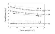
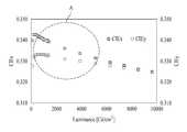
도 2는 형광 소자의 휘도에 따른 효율 변화 특성과, 인광 소자의 휘도에 따른 효율 변화 특성을 나타낸 그래프이고, 도 3은 도 2에 도시된 형광 소자에 대한 색좌표를 나타내고 있다.FIG. 2 is a graph illustrating efficiency change characteristics according to the luminance of the fluorescent element and efficiency change characteristics depending on the luminance of the phosphorescent element, and FIG. 3 illustrates color coordinates of the fluorescent element shown in FIG. 2.
본 발명의 실시 예에 따른 백색 유기 발광 소자는 적색, 녹색, 청색 발광층들을 구비하는 구조로 서로 보색 관계에 있는 두 가지 색의 발광층을 이용하여 백색광을 구현한다. 이때, 백색 유기 발광 소자는 제1 스택(120)으로부터 청색이 발광되며, 제2 스택(140)으로부터 적색 및 녹색이 발광되어 백색 광을 구현한다.The white organic light emitting diode according to the embodiment of the present invention has a structure including red, green, and blue light emitting layers, and realizes white light using two light emitting layers having complementary colors. In this case, blue light is emitted from the
제1 스택(120)의 제1 발광층(128)은 하나의 호스트에 청색 형광 성분의 도펀트가 포함된 발광층이며, 제2 스택(140)의 제2 발광층(146)은 하나의 호스트에 인광 적색 및 인광 녹색 도펀트(phosphorescence Green + phosphorescence Red)를 함께 도핑하여 이루어진 단일 발광층이다. 즉, 제1 발광층(128)은 형광층이며, 제2 발광층(146)은 인광층이다.The first
상술한 바와 같이, 제1 스택(120)의 제1 발광층(128)은 형광층으로 형성되며, 제2 발광층(140)의 제2 발광층(146)은 인광층으로 형성된다. 일반적인 백색 유기 발광 소자는 도 2에 도시된 바와 같은 그래프 특성이 나타난다.As described above, the first
구체적으로, 도 2에 도시된 제1 곡선(202)은 형광 소자의 휘도에 따른 효율 변화 특성을 나타낸 기울기이며, 도 2에 도시된 제2 곡선(204)은 인광 소자의 휘도에 따른 효율 변화 특성을 나타낸 기울기이다.In detail, the
도 2에 도시된 바와 같이 청색 형광층의 제1 곡선(202)은 고휘도 영역으로 갈수록 효율의 변화가 없으나, 적색 및 녹색 인광층의 제2 곡선(204)은 고휘도 영역으로 갈수록 청색 형광층의 제1 곡선(204)에 비해 효율의 변화가 커지고 있다. 이와 같이, 형광 소자와 인광 소자의 휘도에 따른 효율 변화 기울기의 차이로 인해 도 3에 도시된 A 영역과 같이 휘도에 따른 색좌표 변화가 나타난다.As shown in FIG. 2, the
이를 보완하기 위해, 본 발명의 실시 예에 따른 제1 스택(120)은 제1 발광층(128)의 형광 효율을 높이는 동시에 휘도에 따른 효율 변화 기울기를 제2 스택(140)의 제2 발광층(146)에 맞추도록 형성된다. 구체적으로, 제1 스택(120)은 제1 발광층(128)의 형광 효율을 높이기 위해 내부 양자 효율(Internal Quantum Efficiency;IQE)을 높이며, 제2 스택(140)의 제2 발광층(146)의 휘도에 따른 효율 변화 기울기를 맞추기 위해 도펀트의 양을 조절한다. 제1 스택(120)은 내부 양자 효율(IQE)을 높이기 위해 삼중항-삼중항 소멸 현상(Triplet-Triplet Annihilation;TTA)이 잘 일어나는 구조로 형성된다. 이러한, 본 발명의 실시 예에 따른 내부 양자 효율(IQE)을 높이는 제1 스택(120)의 구조에 대해서는 도 4 및 도 5를 결부하여 설명하기로 하며, 제2 스택(140)의 휘도에 따른 효율 변화 기울기를 맞추기 위해 도펀트 양을 조절하는 것에 대해는 도 6을 결부하여 설명하기로 한다.To compensate for this, the
도 4는 본 발명의 실시 예에 따른 제1 스택 구조를 설명하기 위한 단면도이다. 그리고, 도 5는 본 발명의 실시 예에 따른 제1 스택 구조의 내부 양자 효율을 나타내고 있는 단면도이다.4 is a cross-sectional view illustrating a first stack structure according to an embodiment of the present invention. 5 is a cross-sectional view illustrating the internal quantum efficiency of the first stack structure according to the embodiment of the present invention.
본 발명의 실시 예에 따른 제1 스택(120)은 제1 발광층(128) 내에 삼중항-삼중항 소멸 현상(Triplet-Triplet Annihilation; TTA)이 잘 일어날 수 있는 구조로 형성된다. 즉, 삼중항-삼중항 소멸 현상을 통한 지연 형광(Delayed Flurescence)의 기여로 내부 양자 효율(Internal Quantum Efficiency; 이하, IQE)이 향상된다.The
다시 말하여, 삼중항-삼중항 소멸 현상(TTA)을 통한 효율 기여를 위해서는 발광층(128) 내에 삼중항-삼중항 소멸 현상이 효율적으로 잘 일어날 수 있는 소자의 구조를 갖추어야 한다. TTA 현상을 통한 삼중항에서 일중항으로의 전이가 용이하기 위해 발광층의 호스트(Host)와 도펀트(Dopant) 각각의 일중항-삼중항 간의 전이 에너지(Singlet-Triplet 간의 Exchange Energy;△Est)가 작아야 한다. 하지만, 삼중항 엑시톤을 발광층(128) 내에 효과적으로 막아두기 위해 정공 수종층(124,126)과 전자 수송층(129)의 삼중항 에너지가 청색 호스트의 삼중항 에너지보다 높아야 한다.In other words, in order to contribute efficiency through the triplet-triple extinction phenomenon (TTA), it is necessary to have a structure of a device in which the triplet-triple extinction phenomenon can occur efficiently in the
이에 따라, 제1 스택(120)은 도 4에 도시된 바와 같이 TTA 기여를 위해서 제1 발광층(128)에 인접한 정공 수송층(124,126)과 전자 수송층(129)을 호스트의 삼중항 에너지를 고려한 구조로 형성되며, TTA를 통하여 삼중항 엑시톤(Triplet exiton)이 일중항(Singlet)으로 쉽게 전이되기 위한 구조로 형성된다. 이를 위해, 제1 발광층(128)의 호스트의 △Est는 0.1eV ~ 0.6eV 범위 값을 가진다.Accordingly, as shown in FIG. 4, the
제1 또는 제2 정공 수송층(124,126) 중 제1 발광층(128)과 인접한 정공 수송층(124,126)은 도 4에 도시된 바와 같이 제1 발광층(128) 내의 삼중항 에너지 레벨(T1)보다 높게 형성되며, 제1 정공 주입층(122)과의 최저비점유분자궤도(Lowest Unoccupied Molecular Orbital : LUMO) 준위를 고려하여 형성된다. 이와 같이, 제1 또는 제2 정공 수송층(124,126)의 삼중항 에너지 레벨(TH1)이 제1 발광층(128) 내의 삼중항 에너지 레벨(T1)보다 높게 형성됨으로써 제1 발광층(128) 내에 정공이 제1 또는 제2 정공 수송층(124,126)으로 확산(Diffusion)되는 것을 막을 수 있다. 이에 따라, 제1 발광층(128)의 캐리어(carrier)들이 인접한 정공 수송층(124,126)으로 확산되지 않고 발광층(128) 내에 분포하도록 유도될 수 있다.The
제1 전자 수송층(129)은 도 4에 도시된 바와 같이 제1 발광층(128) 내의 삼중항 에너지 레벨(T1)보다 높게 형성되며, 제1 발광층(128)으로부터 정공이 넘어오지 않게 블럭(Bolck) 특성을 고려하여 형성된다. 이와 같이, 제1 전자 수송층(129)의 삼중항 에너지 레벨(TE1)이 제1 발광층(128) 내의 삼중항 에너지 레벨(T1)보다 높게 형성됨으로써 제1 발광층(128) 내에 전자가 제1 전자 수송층(129)으로 확산(Diffusion)되는 것을 막을 수 있다. 이에 따라, 제1 발광층(128)의 캐리어들이 인접한 전자 수송층(129)으로 확산되지 않고 발광층(128) 내에 분포하도록 유도될 수 있다.As shown in FIG. 4, the first
이와 같은 구조로 형성된 제1 스택(120)은 도 5에 도시된 바와 같이 삼중항-삼중항 소멸 현상(Triplet-Triplet Annihilation; TTA)을 통한 지연 형광(Delayed Flurescence)의 기여로 내부 양자 효율(Internal Quantum Efficiency; 이하, IQE)이 25% ~ 50%로 향상되었다. 상술한 제1 스택 구조로 형성한 상태에서 전하들의 이동도를 최적화시켜 고효율 형광 소자를 얻을 수 있다.As shown in FIG. 5, the
도 6은 본 발명의 실시 예에 따른 제1 스택의 도펀트 양을 설명하기 위한 단면도이다.6 is a cross-sectional view illustrating a dopant amount of a first stack according to an exemplary embodiment of the present invention.
본 발명의 실시 예에 따른 제1 스택(120)은 제2 스택(140)의 휘도에 따른 효율 변화 기울기를 고려한 도펀트(Dopant;212)와 호스트(Host;210)의 조합으로 제1 발광층(128)이 형성된다. 다시 말하여, 일반적으로, 형광 소자는 도 1의 제1 곡선(202)과 같은 기울기의 특성을 가지게 되며, 인광 소자는 도 1에 도시된 제2 곡선(204)과 같은 기울기의 특성을 가지게 된다. 도 1를 결부하여 설명한 바와 같이, 형광 소자의 휘도에 따른 효율 변화 기울기와 인광 소자의 휘도에 따른 효율 변화 기울기가 서로 다르게 나타난다.The
이에 따라, 본 발명의 실시 예에 따른 제1 스택(120)은 형광 소자의 제1 곡선(202)을 인광 소자의 제2 곡선(204)과 같이 고휘도 영역으로 갈수록 감소하는 기울기에 가깝도록 일치시키기 위해 제1 발광층(128)의 도펀트의 양을 조절한다. 즉, 제1 발광층(128)은 제2 발광층(146)의 인광 소자와 동일한 휘도 곡선을 나타내도록 도펀트(212)와 호스트(210)를 조합한다.Accordingly, the
구체적으로, 제1 발광층(128)은 도펀트의 농도를 제1 발광층(128)의 중량을 기준으로 4%~10%으로 조절한다. 이와 같이, 도펀트(212)의 농도를 이용하여 농도 소광(Concentration Quenching)의 현상을 적용한다. 즉, 인광 또는 형광 소자에 모두 일어나는 현상으로 도펀트(212)의 농도가 과다할 경우에 발광 효율이 감소하게 된다. 캐리어 호핑을 통해 분자 사이를 이동하게 되는데 도펀트(212)의 농도가 과다하게 되면, 도펀트 입자 내에서 캐리어들 간의 충돌이 발생되어 열화가 일어나는 과정이다. 이러한 농도 소광 현상을 적용하게 되면, 전류 밀도에 따라 한정된 발광층(128) 내에서 서로 충돌하는 캐리어들의 확률이 달라짐으로 인하여 효율에 변화를 줄 수 있다. 이때, 제1 발광층(128)의 도펀트 농도를 증가시킬수록 농도 소광에 의한 휘도 변화에 따른 효율 변화 기울기가 고휘도 영역으로 갈수록 떨어지게 된다. 이에 따라, 제1 발광층(128)의 도펀트의 농도는 제2 발광층(140)의 휘도 특성에 따라 달라질 수 있다. 이와 같이, 제1 발광층(128)은 도펀트의 농도를 증가시켜 휘도 변화에 따른 효율 변화 기울기를 제2 스택(140)의 기울기와 동일한 곡선을 갖게 되어 백색 색 좌표를 해결하였다.Specifically, the first
도 7은 본 발명의 실시 예에 따른 제1 도펀트(D1)와 제1 호스트(H1)를 구성하는 제1 발광층의 도펀트 농도에 따른 휘도 효율을 나타낸 그래프이다.FIG. 7 is a graph showing luminance efficiency according to dopant concentrations of the first emission layer constituting the first dopant D1 and the first host H1 according to an exemplary embodiment of the present invention.
도 7은 제1 도펀트(D1)와 제1 호스트(H1)의 조합의 제1 발광층을 나타내는 곡선이며, 제1 발광층 내에 제1 도펀트(D1)의 양을 달리한 경우 휘도 효율 변화가 달라지는 것을 나타내고 있다. 구체적으로, 도 7에 대한 제1 곡선(230)은 제1 발광층 내에 4%의 제1 도펀트(D1) 농도를 가질 경우에 대한 휘도 곡선이며, 제2 곡선(232)은 제1 발광층 내에 6%의 제1 도펀트(D1) 농도를 가질 경우에 대한 휘도 곡선이며, 제3 곡선(234)은 제1 발광층 내에 8%의 제1 도펀트(D1) 농도를 가질 경우에 대한 휘도 곡선이다. 이와 같이, 휘도 효율 곡선은 제1 발광층 내의 도펀트 양이 증가할수록 기울기가 급해지는 것을 알 수 있다.FIG. 7 is a curve showing a first light emitting layer of a combination of the first dopant D1 and the first host H1, and shows that the luminance efficiency changes when the amount of the first dopant D1 is changed in the first light emitting layer. have. Specifically, the
또한, 제1 호스트(H1)와 제1 도펀트(D1)의 양에 따른 제1 발광층은 [표 1]과 같이 나타낸다. [표 1]은 제1 호스트(H1)와 제1 도펀트(D1) 농도에 따른 구동전압(V), 단위 면적당 휘도(Cd/A), 양자 효율(QE(%)), 색좌표(CIEx, CIEy)를 나타내고 있다.In addition, the first light emitting layer according to the amount of the first host H1 and the first dopant D1 is shown in Table 1 below. [Table 1] shows the driving voltage (V) according to the concentration of the first host (H1) and the first dopant (D1), the luminance per unit area (Cd / A), quantum efficiency (QE (%)), color coordinates (CIEx, CIEy) ).
BH1
BH1
도 8은 본 발명의 실시 예에 따른 제1 도펀트(D1)와 제2 호스트(H2)를 구성하는 제1 발광층의 도펀트 농도에 따른 휘도 효율을 나타낸 그래프이다.FIG. 8 is a graph showing luminance efficiency according to dopant concentrations of the first emission layer constituting the first dopant D1 and the second host H2 according to an exemplary embodiment of the present invention.
도 8은 제1 도펀트(D1)와 제2 호스트(H2)의 조합에 따른 제1 발광층을 나타내는 곡선이며, 제1 발광층 내에 제1 도펀트(D1)의 양을 달리한 경우 휘도 효율 변화가 달라지는 것을 나타내고 있다. 구체적으로, 도 8에 대한 제1 곡선(224)은 제1 발광층 내에 2%의 제1 도펀트(D1) 농도를 가질 경우에 대한 휘도 곡선이며, 제2 곡선(220)은 제1 발광층 내에 4%의 제1 도펀트(D1) 농도를 가질 경우에 대한 휘도 곡선이며, 제3 곡선(226)은 제1 발광층 내에 6%의 제1 도펀트(D1) 농도를 가질 경우에 대한 휘도 곡선이며, 제4 곡선(222)은 제1 발광층 내에 8%의 제1 도펀트(D1) 농도를 가질 경우에 대한 휘도 곡선을 나타내고 있다. 이와 같이, 휘도 효율 곡선은 제1 발광층 내의 도펀트 양이 증가할수록 기울기가 급해지는 것을 알 수 있다.FIG. 8 is a curve illustrating a first light emitting layer according to a combination of the first dopant D1 and the second host H2. When the amount of the first dopant D1 is changed in the first light emitting layer, a change in luminance efficiency is changed. It is shown. Specifically, the
또한, 제2 호스트(H2)와 제1 도펀트(D1)의 양에 따른 제1 발광층은 [표 2]와 같이 나타낸다. [표 2]는 제2 호스트(H1)와 제1 도펀트(D1) 농도에 따른 구동전압(V), 단위 면적당 휘도(Cd/A), 양자 효율(QE(%)), 색좌표(CIEx, CIEy)를 나타내고 있다.In addition, the first light emitting layer according to the amount of the second host H2 and the first dopant D1 is shown in Table 2 below. [Table 2] shows the driving voltage (V) according to the concentration of the second host (H1) and the first dopant (D1), luminance per unit area (Cd / A), quantum efficiency (QE (%)), color coordinates (CIEx, CIEy) ).
BH2
한편, 발광층 내의 도펀트 양뿐만 아니라, 호스트의 종류에 따라 휘도 효율의 기울기가 달라지는 것을 알 수 있다. 이때, 제2 호스트(H2)는 제1 호스트(H1)에 비해 전하 밸런스(Charge balance)가 최적에 가깝게 맞춘 것을 예로 들 수 있다. 이와 같이, 형광의 특성에 따라 도펀트의 농도를 달리하여 휘도 효율 기울기를 변화시킬 수 있으며, 도펀트의 농도 외에 호스트의 종류에 따라서도 휘도 효율 기울기를 변화시킬 수 있다. 이는, 사용자의 필요에 따라 변경할 수 있다.On the other hand, it can be seen that the slope of the luminance efficiency varies depending on the type of host as well as the amount of dopant in the light emitting layer. In this case, the second host H2 may be an example in which the charge balance is closer to the optimum than the first host H1. As such, the luminance efficiency slope may be changed by varying the concentration of the dopant according to the characteristics of the fluorescence, and the luminance efficiency slope may be changed depending on the type of the host in addition to the concentration of the dopant. This can be changed according to the needs of the user.
도 9는 본 발명의 실시 예에 따른 도펀트의 농도는 동일하나, 호스트와 도펀트를 다르게 조합한 경우에 따른 휘도 효율를 나타낸 그래프이다.FIG. 9 is a graph showing luminance efficiency according to the case where the concentration of the dopant is the same but the host and the dopant are differently combined.
도 9는 도펀트의 농도를 8%로 동일하게 적용한 경우를 나타낸 것이며, 도 9에 대한 제1 곡선(244)은 제1 호스트(H1)와 8%의 제1 도펀트(D1)의 농도를 가질 경우(Device B4)에 대한 휘도 곡선이며, 제2 곡선(242)은 제1 호스트(H1)와 8%의 제2 도펀트(D2)의 농도를 가질 경우(Device B3)에 대한 휘도 곡선이며, 제3 곡선(240)은 제2 호스트(H2)와 8%의 제1 도펀트(D1)의 농도를 가질 경우(Device B2)에 대한 휘도 곡선을 나타내고 있다. 이와 같이, 휘도 효율 곡선은 도펀트의 종류와 호스트의 종류에 따라 기울기가 달라질 수 있다.9 illustrates a case where the concentration of the dopant is equally applied to 8%, and the
또한, 도펀트의 종류와 호스트의 종류에 따른 제1 발광층은 [표 3]과 같이 나타낸다. [표 3]은 제1 내지 제3 곡선의 특성을 가지는 제1 발광층 각각의 구동전압(V), 단위 면적당 휘도(Cd/A), 양자 효율(QE(%)), 색좌표(CIEx, CIEy)를 나타내고 있다.In addition, the first light emitting layer according to the type of dopant and the type of host is shown in Table 3 below. [Table 3] shows driving voltage (V), luminance per unit area (Cd / A), quantum efficiency (QE (%)), and color coordinates (CIEx, CIEy) of each of the first light emitting layers having the characteristics of the first to third curves. Indicates.
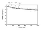
도 10은 도 9에 도시된 각각의 유기 발광 소자에 대한 휘도 변화 기울기를 나타내고 있다.FIG. 10 illustrates a slope of luminance change for each of the organic light emitting diodes shown in FIG. 9.
구체적으로, 도 10에 도시된 제1 곡선(256)은 표 3에 기재된 Device B2에 따른 휘도 변화 기울기를 나타내고 있으며, 제2 곡선(254)는 표 3에 기재된 Device B3에 대한 휘도 변화 기울기를 나타내고 있으며, 제3 곡선(250)은 표 3에 기재된 Device B4에 대한 휘도 변화 기울기를 나타내고 있으며, 제4 곡선(258)은 백색 휘도 변화 기울기를 나타내고 있다. 이와 같이, 본 발명은 도펀트의 농도 조절을 통해 Device B2와 같은 곡선을 가질 수 있어 백색 색좌표 변화가 발생되지 않는다.Specifically, the
이상의 설명은 본 발명을 예시적으로 설명한 것에 불과하며, 본 발명이 속하는 기술 분야에서 통상의 지식을 가진 자에 의해 본 발명의 기술적 사상에서 벗어나지 않는 범위에서 다양한 변형이 가능할 것이다. 따라서 본 발명의 명세서에 개시된 실시 예들은 본 발명을 한정하는 것이 아니다. 본 발명의 범위는 아래의 특허청구범위에 의해 해석되어야 하며, 그와 균등한 범위 내에 있는 모든 기술도 본 발명의 범위에 포함되는 것으로 해석해야 할 것이다.The foregoing description is merely illustrative of the present invention, and various modifications may be made by those skilled in the art without departing from the spirit of the present invention. Accordingly, the embodiments disclosed in the specification of the present invention are not intended to limit the present invention. The scope of the present invention should be construed according to the following claims, and all the techniques within the scope of equivalents should be construed as being included in the scope of the present invention.
100 : 기판110: 제1 전극
120 : 제1 스택122 : 제1 정공 주입층
124 : 제1 정공 수송층126 : 제2 정공 수송층
128 : 제1 발광층129 : 제1 전자 수송층
130 : 전하 생성층140 : 제2 스택
142 : 제2 정공 주입층144 : 제3 정공 수송층
146 : 제2 발광층148 : 제2 전자 수송층
149 : 전자 주입층150 : 제2 전극100 substrate 110: first electrode
120: first stack 122: first hole injection layer
124: first hole transport layer 126: second hole transport layer
128: first emission layer 129: first electron transport layer
130: charge generation layer 140: second stack
142: second hole injection layer 144: third hole transport layer
146: second emission layer 148: second electron transport layer
149: electron injection layer 150: second electrode
Claims (11)
Translated fromKorean상기 제1 전극과 제2 전극 사이에 형성된 전하 생성층과;
상기 제1 전극과 상기 전하 생성층 사이에 형성되고, 형광 성분의 도펀트를 포함하는 제1 발광층을 가지는 제1 스택과;
상기 전하 생성층과 상기 제2 전극 사이에 형성되고, 인광 성분의 도펀트를 포함하는 제2 발광층을 가지는 제2 스택과;
상기 제1 발광층은 상기 제1 전극과 상기 전하 생성층 사이에 삼중항-삼중항 소멸 현상에서 삼중항 엑시톤이 일중항으로 전이할 수 있도록 일중항-삼중항 간의 전이 에너지(△Est)가 작으며, 고휘도 영역으로 갈수록 효율이 감소하는 인광 소자의 제2 발광층의 휘도에 따른 효율 변화 곡선의 기울기와 형광 도펀트를 포함하는 제1 발광층의 휘도에 따른 효율 변화 곡선의 기울기를 맞추기 위해 상기 제1 발광층의 형광 도펀트 농도는 제1 발광층의 중량을 기준으로 4%~10%의 범위로 조절하는 것을 특징으로 하는 백색 유기 발광 소자.A first electrode and a second electrode opposing each other on the substrate;
A charge generation layer formed between the first electrode and the second electrode;
A first stack formed between the first electrode and the charge generation layer and having a first light emitting layer comprising a dopant of a fluorescent component;
A second stack formed between the charge generation layer and the second electrode and having a second light emitting layer comprising a dopant of a phosphorescent component;
The first light emitting layer has a small transition energy (ΔEst) between singlet and triplet so that triplet excitons can be transferred to singlet in the triplet-triple extinction phenomenon between the first electrode and the charge generating layer. In order to adjust the slope of the efficiency change curve according to the luminance of the second light emitting layer of the phosphorescent device having a decreasing efficiency toward the high luminance region and the slope of the efficiency change curve according to the luminance of the first light emitting layer including the fluorescent dopant, Fluorescent dopant concentration is a white organic light emitting device, characterized in that adjusted to the range of 4% to 10% based on the weight of the first light emitting layer.
상기 제1 스택은
상기 제1 전극과 상기 전하 생성층 사이에 제1 정공 주입층, 제1 정공 수송층, 제2 정공 수송층, 상기 제1 발광층 상에 제1 전자 수송층을 더 포함하는 것을 특징으로 하는 백색 유기 발광 소자.The method of claim 1,
The first stack
And a first electron transport layer on the first hole injection layer, the first hole transport layer, the second hole transport layer, and the first light emitting layer between the first electrode and the charge generation layer.
상기 제2 스택은
상기 전하 생성층과 상기 제2 전극 사이에 제2 정공 주입층, 제3 정공 수송층, 상기 제2 발광층 상에 제2 전자 수송층을 더 포함하는 것을 특징으로 하는 백색 유기 발광 소자.3. The method of claim 2,
The second stack is
And a second electron transport layer on the second hole injection layer, the third hole transport layer, and the second light emitting layer between the charge generation layer and the second electrode.
상기 제1 발광층은 하나의 호스트에 청색 형광 성분의 도펀트가 포함된 발광층이며, 상기 제2 발광층은 하나의 호스트에 인광 적색 및 인광 녹색 도펀트를 함께 도핑하여 이루어진 단일 발광층인 것을 특징으로 하는 백색 유기 발광 소자.The method of claim 1,
The first light emitting layer is a light emitting layer including a dopant of a blue fluorescent component in one host, the second light emitting layer is a single light emitting layer formed by doping a phosphorescent red and a phosphorescent green dopant together in one host device.
상기 제1 발광층은 하나의 호스트에 청색 형광 성분의 도펀트가 포함된 발광층이며, 상기 제2 발광층은 하나의 호스트에 인광 엘로우(Yellow)-그린(Green) 도펀트 또는 하나의 호스트에 인광 녹색 도펀트로 이루어진 단일 발광층인 것을 특징으로 하는 백색 유기 발광 소자.The method of claim 1,
The first light emitting layer is a light emitting layer including a dopant of a blue fluorescent component in one host, and the second light emitting layer is formed of a phosphorescent yellow-green dopant in one host or a phosphorescent green dopant in one host. A white organic light emitting device, characterized in that a single light emitting layer.
상기 일중항-삼중항 간의 전이 에너지(△Est)는 0.1eV ~ 0.6eV의 범위에 속하는 것을 특징으로 하는 백색 유기 발광 소자.The method of claim 1,
Transition energy (ΔEst) between the singlet and triplet is in the range of 0.1eV ~ 0.6eV white organic light emitting device.
상기 제1 전자 수송층은 적어도 두 층의 전자 수송층으로 형성되며, 적어도 두 층 중 하나의 전자 수송층은 상기 제1 발광층으로부터 금속 확산을 최소화할 수 있는 재질을 선택하며, 상기 적어도 두 층 중 다른 하나의 전자 수송층은 금속의 도핑을 통한 전자 주입이 가능한 유기물 재질이 사용되는 것을 특징으로 하는 백색 유기 발광 소자.3. The method of claim 2,
The first electron transport layer is formed of at least two electron transport layers, and one of the at least two layers selects a material capable of minimizing metal diffusion from the first light emitting layer, and the other of the at least two layers. The electron transport layer is a white organic light emitting device, characterized in that the organic material which is capable of electron injection through the doping of the metal is used.
상기 적어도 두 층의 전자 수송층 중 상기 제1 발광층과 인접한 전자 수송층은 제1 발광층의 삼중항 에너지 레벨보다 높게 형성되는 것을 특징으로 하는 백색 유기 발광 소자.9. The method of claim 8,
The electron transport layer of the at least two electron transport layer adjacent to the first light emitting layer is formed to be higher than the triplet energy level of the first light emitting layer.
상기 제1 정공 수송층은 상기 제1 발광층의 삼중항 에너지 레벨보다 높게 형성되는 것을 특징으로 하는 백색 유기 발광 소자.3. The method of claim 2,
And the first hole transport layer is formed higher than the triplet energy level of the first light emitting layer.
상기 제2 전자 수송층과 상기 제3 정공 수송층은 상기 제2 발광층의 삼중항 에너지 레벨보다 높게 형성되는 것을 특징으로 하는 백색 유기 발광 소자.The method of claim 3,
And the second electron transporting layer and the third hole transporting layer are formed higher than the triplet energy level of the second light emitting layer.
Priority Applications (4)
| Application Number | Priority Date | Filing Date | Title |
|---|---|---|---|
| KR1020100104975AKR101351417B1 (en) | 2010-10-26 | 2010-10-26 | White organic light emitting device |
| CN201110330141.6ACN102456847B (en) | 2010-10-26 | 2011-10-24 | White organic light emitting device |
| US13/280,725US9159957B2 (en) | 2010-10-26 | 2011-10-25 | White organic light emitting device |
| DE102011054774.6ADE102011054774B4 (en) | 2010-10-26 | 2011-10-25 | WHITE LIGHT EMITTING ORGANIC DEVICES |
Applications Claiming Priority (1)
| Application Number | Priority Date | Filing Date | Title |
|---|---|---|---|
| KR1020100104975AKR101351417B1 (en) | 2010-10-26 | 2010-10-26 | White organic light emitting device |
Publications (2)
| Publication Number | Publication Date |
|---|---|
| KR20120043606A KR20120043606A (en) | 2012-05-04 |
| KR101351417B1true KR101351417B1 (en) | 2014-01-14 |
Family
ID=45923364
Family Applications (1)
| Application Number | Title | Priority Date | Filing Date |
|---|---|---|---|
| KR1020100104975AActiveKR101351417B1 (en) | 2010-10-26 | 2010-10-26 | White organic light emitting device |
Country Status (4)
| Country | Link |
|---|---|
| US (1) | US9159957B2 (en) |
| KR (1) | KR101351417B1 (en) |
| CN (1) | CN102456847B (en) |
| DE (1) | DE102011054774B4 (en) |
Families Citing this family (25)
| Publication number | Priority date | Publication date | Assignee | Title |
|---|---|---|---|---|
| KR101696481B1 (en)* | 2010-10-13 | 2017-01-16 | 엘지디스플레이 주식회사 | Organic Light Emitting Diode And Method Manufacturing Of The Same |
| TWI547208B (en)* | 2012-03-19 | 2016-08-21 | 友達光電股份有限公司 | Organic electroluminescent apparatus |
| GB201207866D0 (en) | 2012-05-04 | 2012-06-20 | Cambridge Display Tech Ltd | Organic light emitting device and method |
| KR101950836B1 (en)* | 2012-05-22 | 2019-02-22 | 엘지디스플레이 주식회사 | Organic light emitting device and method of fabricating the same |
| KR102579507B1 (en) | 2012-08-03 | 2023-09-19 | 가부시키가이샤 한도오따이 에네루기 켄큐쇼 | Light-emitting element, light-emitting device, display device, electronic appliance, and lighting device |
| KR101941453B1 (en)* | 2012-09-28 | 2019-01-23 | 엘지디스플레이 주식회사 | Organic light emitting display device |
| JP6113993B2 (en)* | 2012-10-03 | 2017-04-12 | 出光興産株式会社 | Organic electroluminescence device |
| GB2508092B (en)* | 2012-10-31 | 2015-09-23 | Lg Display Co Ltd | Light emitting device and organic light emitting display device including the same |
| KR20140080606A (en) | 2012-12-12 | 2014-07-01 | 삼성전자주식회사 | Organometallic complexes, organic electroluminescence device using the same and display |
| CN103915470B (en)* | 2012-12-31 | 2016-12-07 | 乐金显示有限公司 | Organic light-emitting display device |
| WO2014157619A1 (en)* | 2013-03-29 | 2014-10-02 | 国立大学法人九州大学 | Organic electroluminescent element |
| KR102059601B1 (en)* | 2013-04-01 | 2019-12-27 | 삼성디스플레이 주식회사 | Organic light emitting diode device |
| KR102060018B1 (en)* | 2013-11-26 | 2019-12-30 | 엘지디스플레이 주식회사 | Organic Light Emitting Device |
| KR102101202B1 (en)* | 2013-12-30 | 2020-04-17 | 엘지디스플레이 주식회사 | Organic Light Emitting Diode And Organic Light Emitting Diode Display Device Including The Same |
| KR101674250B1 (en)* | 2014-02-11 | 2016-11-08 | 단국대학교 산학협력단 | Highly Efficient White OLED |
| JP6307993B2 (en)* | 2014-04-07 | 2018-04-11 | コニカミノルタ株式会社 | ORGANIC ELECTROLUMINESCENT ELEMENT AND ELECTRONIC DEVICE |
| TWI777568B (en) | 2014-05-30 | 2022-09-11 | 日商半導體能源研究所股份有限公司 | Light-emitting element, light-emitting device, electronic device, and lighting device |
| JP2017212024A (en) | 2014-08-28 | 2017-11-30 | 出光興産株式会社 | Organic electroluminescent device and electronic equipment |
| KR102294413B1 (en)* | 2014-11-18 | 2021-08-27 | 삼성디스플레이 주식회사 | Organice light emitting diode display |
| CN109196679B (en)* | 2015-12-01 | 2021-06-08 | 株式会社半导体能源研究所 | Light-emitting element, light-emitting device, electronic equipment and lighting device |
| KR102760908B1 (en) | 2016-12-30 | 2025-01-24 | 엘지디스플레이 주식회사 | Organic light emitting device and organic light emitting display device comprising the same |
| JP6999876B2 (en)* | 2017-07-28 | 2022-01-19 | セイコーエプソン株式会社 | Light emitting elements, display devices, and electronic devices |
| US12193321B2 (en)* | 2019-07-10 | 2025-01-07 | Duk San Neolux Co., Ltd. | Compound for organic electric element, organic electric element comprising the same, and electronic device thereof |
| CN110707226B (en)* | 2019-10-16 | 2022-08-23 | 苏州大学 | Organic light-emitting device, preparation method thereof and light-emitting device |
| KR102743698B1 (en)* | 2020-12-29 | 2024-12-17 | 엘지디스플레이 주식회사 | Organic light emitting diode device and display device using same |
Citations (1)
| Publication number | Priority date | Publication date | Assignee | Title |
|---|---|---|---|---|
| KR20100062169A (en)* | 2008-12-01 | 2010-06-10 | 엘지디스플레이 주식회사 | White organic light emitting device and method for manufacturing the same |
Family Cites Families (7)
| Publication number | Priority date | Publication date | Assignee | Title |
|---|---|---|---|---|
| US7273663B2 (en)* | 2004-08-20 | 2007-09-25 | Eastman Kodak Company | White OLED having multiple white electroluminescence units |
| CN101258621A (en)* | 2005-09-05 | 2008-09-03 | 出光兴产株式会社 | Blue-emitting organic electroluminescent element |
| GB0620045D0 (en)* | 2006-10-10 | 2006-11-22 | Cdt Oxford Ltd | Otpo-electrical devices and methods of making the same |
| WO2008131750A2 (en) | 2007-04-30 | 2008-11-06 | Novaled Ag | Light-emitting component and method for the production thereof |
| KR101316752B1 (en)* | 2007-05-31 | 2013-10-08 | 삼성디스플레이 주식회사 | White organic light emitting display |
| KR101628782B1 (en) | 2009-03-20 | 2016-06-09 | 삼성전자주식회사 | Apparatus and method for providing haptic function using multi vibrator in portable terminal |
| US20100314644A1 (en)* | 2009-06-12 | 2010-12-16 | Idemitsu Kosan Co., Ltd. | Organic electroluminescent device |
- 2010
- 2010-10-26KRKR1020100104975Apatent/KR101351417B1/enactiveActive
- 2011
- 2011-10-24CNCN201110330141.6Apatent/CN102456847B/enactiveActive
- 2011-10-25USUS13/280,725patent/US9159957B2/enactiveActive
- 2011-10-25DEDE102011054774.6Apatent/DE102011054774B4/enactiveActive
Patent Citations (1)
| Publication number | Priority date | Publication date | Assignee | Title |
|---|---|---|---|---|
| KR20100062169A (en)* | 2008-12-01 | 2010-06-10 | 엘지디스플레이 주식회사 | White organic light emitting device and method for manufacturing the same |
Non-Patent Citations (1)
| Title |
|---|
| "The singlet-triplet exchange energy in conjugated polymets", Advanced Functional Materials, 14; pages 11-18, January 2004.* |
Also Published As
| Publication number | Publication date |
|---|---|
| CN102456847A (en) | 2012-05-16 |
| US20120097998A1 (en) | 2012-04-26 |
| US9159957B2 (en) | 2015-10-13 |
| CN102456847B (en) | 2016-08-10 |
| DE102011054774B4 (en) | 2018-05-03 |
| DE102011054774A9 (en) | 2012-07-19 |
| KR20120043606A (en) | 2012-05-04 |
| DE102011054774A1 (en) | 2012-04-26 |
Similar Documents
| Publication | Publication Date | Title |
|---|---|---|
| KR101351417B1 (en) | White organic light emitting device | |
| US20240188320A1 (en) | Organic electroluminescent devices | |
| TW543337B (en) | Highly stable and efficient OLEDs with a phosphorescent-doped mixed layer architecture | |
| KR102126544B1 (en) | Organic electroluminescent device and organic electroluminescent display | |
| KR102089329B1 (en) | Organic light emitting display | |
| KR102104978B1 (en) | Organic light emitting display and method for fabricating the same | |
| KR101786881B1 (en) | White organic light emitting device | |
| CN106848084B (en) | An OLED display panel, manufacturing method and electronic device containing the same | |
| CN102034934A (en) | White organic light emitting device | |
| US11700756B2 (en) | Energy efficient OLED TV | |
| KR20140079273A (en) | White organic light emitting device | |
| US10084146B2 (en) | Organic electroluminescent element and lighting device | |
| KR102797907B1 (en) | Oled display panel with unpatterned emissive stack | |
| CN105304822B (en) | White organic light emitting device | |
| CN106654033A (en) | Organic light emitting display panel and electronic equipment | |
| KR101715857B1 (en) | White Organic Emitting Device | |
| CN108987594B (en) | Organic electroluminescent diode and organic electroluminescent device | |
| KR101777123B1 (en) | White organic light emitting device | |
| KR101777124B1 (en) | White organic light emitting device | |
| KR20220031867A (en) | Organic light emitting display device | |
| CN108023022A (en) | A kind of organic electroluminescence device and electronic equipment | |
| KR102009804B1 (en) | Organic light emitting diode display device and method for manufacturing the same | |
| KR102081122B1 (en) | Organic light emitting display | |
| KR20210031675A (en) | White organic light emitting device |
Legal Events
| Date | Code | Title | Description |
|---|---|---|---|
| PA0109 | Patent application | Patent event code:PA01091R01D Comment text:Patent Application Patent event date:20101026 | |
| A201 | Request for examination | ||
| PA0201 | Request for examination | Patent event code:PA02012R01D Patent event date:20111107 Comment text:Request for Examination of Application Patent event code:PA02011R01I Patent event date:20101026 Comment text:Patent Application | |
| PG1501 | Laying open of application | ||
| E902 | Notification of reason for refusal | ||
| PE0902 | Notice of grounds for rejection | Comment text:Notification of reason for refusal Patent event date:20130528 Patent event code:PE09021S01D | |
| E701 | Decision to grant or registration of patent right | ||
| PE0701 | Decision of registration | Patent event code:PE07011S01D Comment text:Decision to Grant Registration Patent event date:20131120 | |
| GRNT | Written decision to grant | ||
| PR0701 | Registration of establishment | Comment text:Registration of Establishment Patent event date:20140108 Patent event code:PR07011E01D | |
| PR1002 | Payment of registration fee | Payment date:20140109 End annual number:3 Start annual number:1 | |
| PG1601 | Publication of registration | ||
| FPAY | Annual fee payment | Payment date:20161214 Year of fee payment:4 | |
| PR1001 | Payment of annual fee | Payment date:20161214 Start annual number:4 End annual number:4 | |
| FPAY | Annual fee payment | Payment date:20171218 Year of fee payment:5 | |
| PR1001 | Payment of annual fee | Payment date:20171218 Start annual number:5 End annual number:5 | |
| FPAY | Annual fee payment | Payment date:20181226 Year of fee payment:6 | |
| PR1001 | Payment of annual fee | Payment date:20181226 Start annual number:6 End annual number:6 | |
| FPAY | Annual fee payment | Payment date:20191212 Year of fee payment:7 | |
| PR1001 | Payment of annual fee | Payment date:20191212 Start annual number:7 End annual number:7 | |
| PR1001 | Payment of annual fee | Payment date:20201222 Start annual number:8 End annual number:8 | |
| PR1001 | Payment of annual fee | Payment date:20241216 Start annual number:12 End annual number:12 |