KR101351410B1 - White Organic Light Emitting Device - Google Patents
White Organic Light Emitting DeviceDownload PDFInfo
- Publication number
- KR101351410B1 KR101351410B1KR1020090092596AKR20090092596AKR101351410B1KR 101351410 B1KR101351410 B1KR 101351410B1KR 1020090092596 AKR1020090092596 AKR 1020090092596AKR 20090092596 AKR20090092596 AKR 20090092596AKR 101351410 B1KR101351410 B1KR 101351410B1
- Authority
- KR
- South Korea
- Prior art keywords
- layer
- light emitting
- electron transport
- transport layer
- energy level
- Prior art date
- Legal status (The legal status is an assumption and is not a legal conclusion. Google has not performed a legal analysis and makes no representation as to the accuracy of the status listed.)
- Active
Links
Images


Classifications
- H—ELECTRICITY
- H10—SEMICONDUCTOR DEVICES; ELECTRIC SOLID-STATE DEVICES NOT OTHERWISE PROVIDED FOR
- H10K—ORGANIC ELECTRIC SOLID-STATE DEVICES
- H10K50/00—Organic light-emitting devices
- H10K50/10—OLEDs or polymer light-emitting diodes [PLED]
- H10K50/11—OLEDs or polymer light-emitting diodes [PLED] characterised by the electroluminescent [EL] layers
- H10K50/125—OLEDs or polymer light-emitting diodes [PLED] characterised by the electroluminescent [EL] layers specially adapted for multicolour light emission, e.g. for emitting white light
- H—ELECTRICITY
- H05—ELECTRIC TECHNIQUES NOT OTHERWISE PROVIDED FOR
- H05B—ELECTRIC HEATING; ELECTRIC LIGHT SOURCES NOT OTHERWISE PROVIDED FOR; CIRCUIT ARRANGEMENTS FOR ELECTRIC LIGHT SOURCES, IN GENERAL
- H05B33/00—Electroluminescent light sources
- H05B33/12—Light sources with substantially two-dimensional radiating surfaces
- H05B33/14—Light sources with substantially two-dimensional radiating surfaces characterised by the chemical or physical composition or the arrangement of the electroluminescent material, or by the simultaneous addition of the electroluminescent material in or onto the light source
- H—ELECTRICITY
- H10—SEMICONDUCTOR DEVICES; ELECTRIC SOLID-STATE DEVICES NOT OTHERWISE PROVIDED FOR
- H10K—ORGANIC ELECTRIC SOLID-STATE DEVICES
- H10K50/00—Organic light-emitting devices
- H—ELECTRICITY
- H10—SEMICONDUCTOR DEVICES; ELECTRIC SOLID-STATE DEVICES NOT OTHERWISE PROVIDED FOR
- H10K—ORGANIC ELECTRIC SOLID-STATE DEVICES
- H10K2101/00—Properties of the organic materials covered by group H10K85/00
- H10K2101/30—Highest occupied molecular orbital [HOMO], lowest unoccupied molecular orbital [LUMO] or Fermi energy values
- H—ELECTRICITY
- H10—SEMICONDUCTOR DEVICES; ELECTRIC SOLID-STATE DEVICES NOT OTHERWISE PROVIDED FOR
- H10K—ORGANIC ELECTRIC SOLID-STATE DEVICES
- H10K50/00—Organic light-emitting devices
- H10K50/10—OLEDs or polymer light-emitting diodes [PLED]
- H10K50/11—OLEDs or polymer light-emitting diodes [PLED] characterised by the electroluminescent [EL] layers
- H10K50/125—OLEDs or polymer light-emitting diodes [PLED] characterised by the electroluminescent [EL] layers specially adapted for multicolour light emission, e.g. for emitting white light
- H10K50/13—OLEDs or polymer light-emitting diodes [PLED] characterised by the electroluminescent [EL] layers specially adapted for multicolour light emission, e.g. for emitting white light comprising stacked EL layers within one EL unit
- H10K50/131—OLEDs or polymer light-emitting diodes [PLED] characterised by the electroluminescent [EL] layers specially adapted for multicolour light emission, e.g. for emitting white light comprising stacked EL layers within one EL unit with spacer layers between the electroluminescent layers
- H—ELECTRICITY
- H10—SEMICONDUCTOR DEVICES; ELECTRIC SOLID-STATE DEVICES NOT OTHERWISE PROVIDED FOR
- H10K—ORGANIC ELECTRIC SOLID-STATE DEVICES
- H10K59/00—Integrated devices, or assemblies of multiple devices, comprising at least one organic light-emitting element covered by group H10K50/00
- H10K59/30—Devices specially adapted for multicolour light emission
- H10K59/32—Stacked devices having two or more layers, each emitting at different wavelengths
Landscapes
- Physics & Mathematics (AREA)
- Optics & Photonics (AREA)
- Electroluminescent Light Sources (AREA)
Abstract
Translated fromKoreanDescription
Translated fromKorean본 발명은 유기 발광 소자에 관한 것으로 특히, 청색 형광과 적색/녹색 인광의 스택 구조로 이루어진 백색 유기 발광 소자에 있어서, 상기 청색 형광의 효율을 높여 상기 백색 유기 발광 소자의 수명을 증가시키고 색감 향상과 소비 전력을 감소시킨 백색 유기 발광 소자에 관한 것이다.The present invention relates to an organic light emitting device, and in particular, in a white organic light emitting device having a stack structure of blue fluorescence and red / green phosphorescence, the efficiency of the blue fluorescence is increased to increase the lifespan of the white organic light emitting device and to improve color. The present invention relates to a white organic light emitting device having reduced power consumption.
최근, 본격적인 정보화 시대로 접어듦에 따라 전기적 정보신호를 시각적으로 표현하는 디스플레이(display) 분야가 급속도로 발전해 왔고, 이에 부응하여 박형화, 경량화, 저소비전력화의 우수한 성능을 지닌 여러 가지 다양한 평판 표시장치(Flat Display Device)가 개발되어 기존의 브라운관(Cathode Ray Tube : CRT)을 빠르게 대체하고 있다.In recent years, as the information age has come to a full-fledged information age, a display field for visually expressing electrical information signals has been rapidly developed. In response to this, various flat panel display devices having excellent performance of thinning, light weight, Flat Display Device) has been developed to replace CRT (Cathode Ray Tube).
이 같은 평판 표시장치의 구체적인 예로는 액정표시장치(Liquid Crystal Display device: LCD), 플라즈마표시장치(Plasma Display Panel device: PDP), 전계방출표시장치(Field Emission Display device: FED), 유기 발광 표시 장치(Organic Light Emitting Device: OLED) 등을 들 수 있다.Specific examples of such flat panel display devices include a liquid crystal display device (LCD), a plasma display panel (PDP), a field emission display (FED) (Organic Light Emitting Device: OLED).
이 중, 별도의 광원을 요구하지 않으며 장치의 컴팩트화 및 선명한 컬러 표 시를 위해 유기 발광 표시 장치가 경쟁력 있는 어플리케이션으로 고려되고 있다.Among them, the organic light emitting diode display is considered to be a competitive application for the compactness and vivid color display of the device without requiring a separate light source.
이러한 유기 발광 표시 장치에는, 유기 발광층의 형성이 필수적인데, 종래 그 형성을 위해 새도우 마스크(shadow mask)를 이용한 증착 방법이 이용되었다.Formation of an organic light emitting layer is essential for the organic light emitting diode display, and a deposition method using a shadow mask has been conventionally used for the formation thereof.
그러나, 새도우 마스크는 대면적의 경우, 그 하중 때문에, 쳐짐 현상이 발생하고, 이로 인해 여러번 이용이 힘들고, 유기 발광층 패턴 형성에 불량이 발생하여 대안적 방법이 요구되었다.However, in the case of a large area, the shadow mask has a drooping phenomenon due to its load, which makes it difficult to use it several times, and a defect occurs in the formation of the organic light emitting layer pattern, and thus an alternative method is required.
이러한 새도우 마스크를 대체하여 여러 방법이 제시되었던 그 중 하나로서 백색 유기 발광 표시 장치가 있다.As one of the various methods for replacing such a shadow mask, there is a white organic light emitting display.
이하, 백색 유기 발광 표시 장치에 대해 설명하면 다음과 같다.Hereinafter, a white organic light emitting display will be described.
백색 유기 발광 표시 장치는, 발광 다이오드 형성시 양극과 음극 사이의 각 층을 마스크 없이 증착시키는 것으로, 유기발광층을 포함한 유기막들의 형성을 차례로 그 성분을 달리하여 진공 상태에서 증착하는 것을 특징으로 한다.The white organic light emitting display device is characterized in that when forming a light emitting diode, each layer between an anode and a cathode is vapor-deposited without a mask, and organic layers including an organic light emitting layer are sequentially deposited in a vacuum state with different components.
상기 백색 유기 발광 표시 장치는, 박형 광원, 액정표시장치의 백라이트 또는 컬러 필터를 채용한 풀컬러 표시 장치에 쓰일 수 있는 등 여러 용도를 가지고 있는 소자이다.The white organic light emitting display device has various uses such as a thin light source, a backlight of a liquid crystal display device, or a full color display device employing a color filter.
상기 백색 유기 발광 표시 장치는 구비되는 발광층을 서로 다른 색상의 복수층으로 구비할 수 있는데, 이 경우, 각 발광층에 포함되는 도펀트 색상을 달리하게 된다. 그러나, 도펀트가 자체적으로 갖는 특성에 의해 해당 발광층에 포함되는 도펀트의 성분에 한계가 있고, 각 발광층의 혼합시 백색광 구현에 초점이 맞춰져 적(Red), 녹(Green), 청(Blue)이 아닌 다른 색상의 파장에서 피크 값을 갖는 파장 특성을 나타내어 컬러 필터 포함시 색재현율이 떨어지는 문제가 있었다. 또한, 도펀트 물질의 수명이 달라 계속적인 이용시 컬러 쉬프트가 발생하였다.The white organic light emitting diode display may include a plurality of light emitting layers having different colors. In this case, the dopant color included in each light emitting layer is changed. However, due to the characteristics of the dopant itself, there is a limit to the components of the dopant included in the light emitting layer, and when the light emitting layers are mixed, the white light is focused to realize red, green, and blue. There was a problem in that the color reproducibility is lowered when the color filter is included because the wavelength characteristic has a peak value at a different color wavelength. In addition, the lifetime of the dopant material is different, resulting in color shifts during continuous use.
더불어, 발광층과 정공 수송층간의 계면에서 그 에너지 준위가 유사하여, 삼중항 여기자가 계면을 넘어 정공 수송층으로 이동하여 여기 상태의 발광효율이 저하되는 문제가 있었고, 이를 방지하기 위해 여기자 저지층(EBL: Exciton Blocking Layer)을 구비할 경우 구동 전압의 증가 및 공정의 증가 및 수명 저하가 수반되어 적정한 효율을 갖는 백색 유기 발광 표시 장치를 구현하는데 많은 애로사항이 있다.In addition, since the energy level is similar at the interface between the light emitting layer and the hole transport layer, the triplet excitons move beyond the interface to the hole transport layer to reduce the luminous efficiency of the excited state. Exciton Blocking Layer) has a number of difficulties in implementing a white organic light emitting display device having an appropriate efficiency due to an increase in driving voltage, an increase in a process, and a decrease in lifespan.
종래 백색 유기 발광 소자는 수명과 소비 전력 측면을 고려했을 때, 적층되어 이루어진 발광층이 모두 형광 구조이거나 혹은 청색 형광층과 적색/녹색 인광의 스택 구조로 이루어진 구조를 이용하였다. 이 두 구조에서 공통적인 점은 일중항 여기 상태의 엑시톤만을 이용하는 청색 형광층의 사용이다.In consideration of the lifespan and the power consumption, the conventional white organic light emitting device uses a structure in which all of the stacked light emitting layers are fluorescent structures or stack structures of blue fluorescent layers and red / green phosphorescent layers. Common to both structures is the use of a blue fluorescent layer using only exciton in singlet excited state.
근래의 기술 수준에서의 청색 인광층의 효율은 만족할만한 수준에 이르렀지만, 수명 측면에서 아직까지 개선이 시급한 상황이다. 이런 이유로 청색 형광층이 적용된 백색 유기 발광 소자가 주로 개발되고 있지만, 색온도 및 수명, 소비전력 개선에는 위에서 언급된 효율 문제로 인하여 제한적이다. 특히, 이를 해결하기 위해서는 내부 양자 효율이 25 %로 제한적인 청색 형광층의 효율과 수명을 개선하는 방법이 필요하다.Although the efficiency of the blue phosphor layer has reached a satisfactory level in recent years, improvements in terms of lifespan are still urgent. For this reason, the white organic light emitting device to which the blue fluorescent layer is applied is mainly developed, but the color temperature, life, and power consumption are limited due to the above-mentioned efficiency problems. In particular, to solve this problem, there is a need for a method of improving the efficiency and lifetime of the blue fluorescent layer having an internal quantum efficiency of 25%.
본 발명은 상기와 같은 문제점을 해결하기 위해 안출한 것으로 청색 형광과 적색/녹색 인광의 스택(stack) 구조로 이루어진 백색 유기 발광 소자에 있어서, 상기 청색 형광의 효율을 높여 상기 백색 유기 발광 소자의 수명을 증가시키고 색감 향상과 소비 전력을 감소시킨 백색 유기 발광 소자를 제공하는 데, 그 목적이 있다.The present invention has been made to solve the above problems, in the white organic light emitting device consisting of a stack structure of blue fluorescence and red / green phosphorescence, the efficiency of the blue fluorescence to increase the lifetime of the white organic light emitting device To provide a white organic light emitting device that increases the color and improve the color and reduced power consumption, the object is.
상기와 같은 목적을 달성하기 위한 본 발명의 백색 유기 발광 소자는, 기판 상에 서로 대향된 양극과 음극;과, 상기 양극과 음극 사이에 형성된 전하 생성층; 과, 상기 양극과 전하 생성층 사이의, 제 1 정공 수송층, 청색을 발광하는 제 1 발광층, 제 1 전자 수송층 및 금속이 도핑된 전자수송 촉매층이 적층되어 이루어진 제 1 스택; 및 상기 전하 생성층과 상기 음극 사이의, 제 2 정공 수송층, 하나의 호스트에 인광의 적색과 녹색 도펀트를 함께 도핑한 제 2 발광층 및 제 2 전자 수송층이 적층되어 이루어지며, 상기 제 2 정공 수송층은 에너지 준위를 상기 제 2 발광층의 삼중항(triplet) 여기 상태 에너지 준위보다 높게 설정한 제 2 스택을 포함하여 이루어진 것에 그 특징이 있다.The white organic light emitting device of the present invention for achieving the above object, an anode and a cathode facing each other on a substrate; and a charge generating layer formed between the anode and the cathode; A first stack formed by stacking a first hole transport layer, a first light emitting layer emitting blue light, a first electron transporting layer, and an electron transport catalyst layer doped with metal between the anode and the charge generating layer; And a second hole transport layer between the charge generation layer and the cathode, a second light emitting layer and a second electron transport layer doped together with a phosphorescent red and green dopant on one host, and the second hole transport layer is And a second stack in which an energy level is set higher than a triplet excited state energy level of the second light emitting layer.
여기서, 상기 제 2 정공 수송층은 상기 제 2 발광층의 삼중항 여기 상태의 에너지 준위보다 0.01~0.4 eV 높은 에너지 준위로 설정한 것이 바람직하다.Here, the second hole transport layer is preferably set to an energy level of 0.01 ~ 0.4 eV higher than the energy level of the triplet excited state of the second light emitting layer.
또한, 상기 제 1 정공 수송층은 상기 제 1 발광층의 삼중항 여기 상태의 에너지 준위보다 0.01~0.4 eV 높은 에너지 준위로 설정한 것이 바람직하다.The first hole transport layer is preferably set to an energy level of 0.01 to 0.4 eV higher than the energy level of the triplet excited state of the first light emitting layer.
그리고, 상기 제 1 전자 수송층은 상기 제 1 발광층의 삼중항 여기 상태의 에너지 준위보다 0.01~0.4eV 높은 에너지 준위로 설정하며, 상기 제 2 전자 수송층은 상기 제 2 발광층의 삼중항 여기 상태의 에너지 준위보다 0.01~0.4eV 높은 에너지 준위로 설정한다.The first electron transport layer is set at an energy level of 0.01 to 0.4 eV higher than the energy level of the triplet excited state of the first emission layer, and the second electron transport layer is an energy level of the triplet excited state of the second emission layer. Set the energy level to 0.01 to 0.4 eV higher.
상기 제 1 발광층은 청색 호스트에 청색을 형광 발광하는 도펀트가 포함되어 이루어진 발광층이다.The first light emitting layer is a light emitting layer including a dopant for fluorescing blue light in a blue host.
상기 전자 수송 촉매층은 상기 제 1 발광층으로의 금속 확산을 최소화함과 동시에 높은 삼중항 에너지 준위를 가지는 재료에서 선택하며, 상기 제 1 전자 수송층은 금속의 도핑을 통한 전자 주입이 가능한 유기물에서 선택할 수 있다.The electron transport catalyst layer may be selected from a material having a high triplet energy level while minimizing metal diffusion into the first light emitting layer, and the first electron transport layer may be selected from organic materials capable of electron injection through doping of metal. .
또한, 상기 제 1 전자 수송층은 bphen 계열의 유기물에서 선택한다.In addition, the first electron transport layer is selected from bphen organic compounds.
한편, 상기 전자수송 촉매층에 도핑된 금속은, 알칼리 금속, MoOx, WOx, V2O5 중 적어도 어느 하나를 포함한다. 예를 들어, 알칼리 금속으로는 Li을 들 수 있다.On the other hand, the metal doped in the electron transport catalyst layer, at least one of an alkali metal, MoOx, WOx, V2 O5 . For example, Li is mentioned as an alkali metal.
그리고, 상기 제 1 스택의 수명이 상기 제 2 스택의 수명보다 길며, 에이징에 따라 쿨 화이트 색특성을 갖는 것이 바람직하다.In addition, the life of the first stack is longer than the life of the second stack, it is preferable to have a cool white color characteristics according to the aging.
상기와 같은 본 발명의 백색 유기 발광 소자는 다음과 같은 효과가 있다.The white organic light emitting device of the present invention has the following effects.
본 발명의 유기 발광 소자는 높은 삼중항 에너지를 갖는 정공층과 금속 도핑된 이중 전자 수송층 구조 적용을 통해 삼중항 쌍 소멸(triplet-triplet annihilation)을 이용하여 청색 형광의 효율을 높이고 수명을 증가시켜 색감 및 저소비전력을 꾀할 수 있다.The organic light emitting device of the present invention improves the efficiency of blue fluorescence and increases the lifespan by using triplet-triplet annihilation through the application of a hole layer and a metal-doped double electron transport layer structure having a high triplet energy. And low power consumption can be achieved.
또한, 양극과 음극 사이의 각 스택에 청색 발광층 및 녹색과 적색의 혼합 발광층을 구비한 이중 스택으로 백색 유기 발광 소자를 형성시, 녹색과 적색의 혼합 발광층에서, 여기 상태의 에너지 준위에 비해 인접한 정공 수송층의 에너지 준위를 0.01~0.4eV 높게 설정하여, 여기 상태의 여기자가 정공 수송층으로 유입되는 것을 방지한다. 따라서, 상기 정공 수송층은 정공 수송의 기능과 함께 여기자 저지 기능(Exciton (singlet, triplet) blocking layer)을 동시에 수행하여 별도로 여기자 저지층을 구비하지 않음에 의해 공정을 늘리지 않으며 소비 전력을 저감할 수 있 다. 더불어, 상기 발광층에 남아있는 일중항 여기자(singlet exciton) 및 삼중항 여기자(triplet excition)의 성분이 계속적으로 발광에 이용되어, 발광효율의 향상시킬 수 있다.In addition, when a white organic light emitting device is formed by a double stack having a blue light emitting layer and a green and red mixed light emitting layer in each stack between the anode and the cathode, in the mixed light emitting layer of green and red, holes adjacent to the energy level of the excited state are formed. The energy level of the transport layer is set to 0.01 to 0.4 eV to prevent the excitons in the excited state from flowing into the hole transport layer. Accordingly, the hole transport layer simultaneously performs an exciton blocking function (Exciton (singlet, triplet) blocking layer) together with a hole transport function, thereby not increasing the process and reducing power consumption by not having an exciton blocking layer separately. All. In addition, the components of singlet exciton and triplet excition remaining in the light emitting layer are continuously used for light emission, thereby improving luminous efficiency.
더불어, 백색을 구현함에 있어서, 일 스택을 청색 도펀트를 포함한 청색 형광 발광층으로 구성하고, 나머지 스택을 호스트 물질에 녹색 및 적색 도펀트를 적정량 포함한 적색/녹색 인광 발광층으로 형성하여, 적색, 녹색 및 청색의 각 파장에서 고른 피크치와 뚜렷한 피크를 보일 수 있어 컬러 필터 적용시 색재현율을 높일 수 있다.In addition, in the implementation of white, one stack is composed of a blue fluorescent light emitting layer including a blue dopant, and the remaining stack is formed of a red / green phosphorescent light emitting layer containing an appropriate amount of green and red dopants in a host material, thereby forming red, green, and blue colors. Even peaks and clear peaks can be seen at each wavelength, increasing color reproducibility when color filters are applied.
이하, 첨부된 도면을 참조하여 본 발명의 백색 유기 발광 소자를 상세히 설명하면 다음과 같다.Hereinafter, the white organic light emitting device of the present invention will be described in detail with reference to the accompanying drawings.
도 1은 본 발명의 백색 유기 발광 소자의 일예를 나타낸 단면도이다.1 is a cross-sectional view showing an example of a white organic light emitting device of the present invention.
도 1과 같이, 본 발명의 일예에 다른, 백색 유기 발광 소자는, 기판(100) 상에 서로 대향된 양극(101)과 음극(140), 상기 양극(101)과 음극(140) 사이에 적층되어 이루어진 제 1 스택(210), 전하생성층 (CGL: Charge Generation Layer)(230) 및 제 2 스택(220)을 포함하여 이루어진다.As shown in FIG. 1, a white organic light emitting diode according to an exemplary embodiment of the present invention is stacked between an anode 101 and a
여기서, 상기 전하 생성층(230)은 아래로부터 금속층(113) 및 제 2 정공 주입층(120)의 적층체로 이루어진다.Here, the charge generation layer 230 is formed of a laminate of the metal layer 113 and the second
그리고, 양극(101)은 ITO(Indium Tin Oxide)와 같은 투명 전극으로 이루어지 며, 상기 음극(140)은 Al(알루미늄)과 같이 반사성 금속으로 이루어지며, 이러한 배치에 의해 각각의 제 1, 제 2 스택(210, 220)에서 이루어지는 발광효과로 도시된 도면을 기준으로 하측으로 이미지가 출사되게 된다.The anode 101 is made of a transparent electrode such as indium tin oxide (ITO), and the
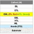
상기 제 1 스택(210)은 상기 양극(101) 상부과 상기 전하생성층(230) 사이에 제 1 정공 전달층(HIL(Hole Injection Layer), 103), 제 1 정공수송층(HTL(Hole Transport Layer), 105), 제 1 발광층(110), 제 1 전자 수송층(ETL(Electron Transport Layer), 111)이 차례로 적층되어 있으며, 상기 제 2 스택(220)은 상기 전하 생성층(230)과 상기 음극(140) 사이에, 차례로, 제 2 정공 수송층(135), 여기자 저지층(EBL: Electron Blocking Layer)(125), 제 2 발광층(130), 제 2 전자 수송층(133) 및 전자 주입층(135)이 적층되어 있다.The
여기서, 상기 제 1 발광층(110)은 청색광의 하나의 호스트에 청색 형광 성분의 도펀트가 포함된 발광층이며, 상기 제 2 발광층(130)은 하나의 호스트에 인광 적색 및 인광 녹색 도펀트(phosphorescence Green +phosphorescence Red)를 함께 도핑하여 이루어진 단일 발광층이다.Here, the first
이 경우, 백색 유기 발광 소자의 구동시 상기 제 1 발광층(110)과 제 2 발광층(130)에서 발광되는 광의 혼합 효과의 의해 백색광이 구현될 수 있다.In this case, white light may be realized by a mixing effect of light emitted from the first
여기서, 상기 제 2 정공 수송층(123)은 상기 제 2 발광층(130)의 삼중항(triplet) 여기자(exciton)의 여기 상태의 에너지 준위보다 높은 에너지 준위를 갖는 것으로 설정한다. 이 경우, 상기 제 2 정공 수송층(125)의 에너지 준위는 상기 제 2 발광층(130)의 삼중항 여기자의 여기 상태의 에너지 준위보다 0.01~0.4eV 정도 높게 설정하는 것이 바람직하다. 이 때, 상기 제 2 발광층(130)보다 상기 제 2 정공 수송층(123)의 에너지 준위가 높기 때문에, 상기 제 2 발광층(130)의 삼중항 여기자(triplet exciton)이 상기 제 2 정공 수송층(123)으로 넘어가 발광 효율이 떨어지는 것을 방지할 수 있다. 즉, 여기서, 상기 제 2 정공 수송층(123)은 고유의 상기 제 2발광층(130)으로부터의 정공의 수송 기능을 하며, 그 상부의 여기자 저지층(125)은 상기 제 2 발광층(130)의 삼중항 여기자가 넘어오는 것을 방지(exciton blocking) 하도록 기능한다.Here, the second
도 2는 도 1의 수명을 개선한 본 발명의 백색 유기 발광 소자의 다른 실시예를 나타낸 단면도이다.FIG. 2 is a cross-sectional view illustrating another embodiment of the white organic light emitting diode of the present invention having improved lifetime of FIG. 1.
도 2의 본 발명의 유기 발광 소자의 다른 실시예에 따른 구조는, 상술한 도 1의 구조와 비교하여, 여기자 저지층(EBL) 층을 생략하고, 상기 전하생성층(CGL)이 제 2 정공 전달층의 단일층으로 이루어지며, 그 하측의 제 1 스택(410)의 제 1 전자 전달층이 상기 제 2 정공 전달층과 인접하여 차례로 적층된 전자수송 촉매층(320)과, 제 1 전자 수송층(315)으로 이루어진 점이 상이하다.The structure according to another embodiment of the organic light emitting device of FIG. 2 omits the exciton blocking layer (EBL) layer, and the charge generation layer (CGL) has a second hole compared with the structure of FIG. 1 described above. An electron transport catalyst layer 320 and a first electron transport layer each having a single layer of a transport layer, in which a first electron transport layer of a lower first stack 410 is sequentially stacked adjacent to the second hole transport layer. 315).
즉, 도 2와 같이, 본 발명의 다른 실시예에 따른, 백색 유기 발광 소자는, 기판(300) 상에 서로 대향된 양극(301)과 음극(340), 상기 양극(301)과 음극(340) 사이에 적층되어 이루어진 제 1 스택(410), 전하생성층 (CGL: Charge Generation Layer)(323) 및 제 2 스택(420)을 포함하여 이루어진다.That is, as shown in FIG. 2, a white organic light emitting diode according to another exemplary embodiment of the present invention includes an anode 301 and a
그리고, 양극(301)은 ITO(Indium Tin Oxide)와 같은 투명 전극으로 이루어지 며, 상기 음극(340)은 Al(알루미늄)과 같이 반사성 금속으로 이루어지며, 이러한 배치에 의해 각각의 제 1, 제 2 스택(410, 420)에서 이루어지는 발광효과로 도시된 도면을 기준으로 하측으로 이미지가 출사되게 된다.In addition, the anode 301 is made of a transparent electrode such as indium tin oxide (ITO), and the
상기 제 1 스택(410)은 상기 양극(301) 상부와 상기 전하생성층(323) 사이에 제 1 정공 전달층(HIL(Hole Injection Layer), 303), 제 1 정공수송층(HTL(Hole Transport Layer), 305), 제 1 발광층(310), 제 1 전자 수송층(ETL(Electron Transport Layer), 315) 및 전자 수송 촉매층(320)이 차례로 적층되어 있으며, 상기 제 2 스택(420)은 상기 전하 생성층(323)과 상기 음극(340) 사이에, 차례로, 제 2 정공 수송층(325), 제 2 발광층(330), 제 2 전자 수송층(333) 및 전자 주입층(336)이 적층되어 있다.The first stack 410 may include a first hole injection layer (HIL) 303 and a first hole transport layer (HTL) between the anode 301 and the charge generation layer 323. ), 305, a first emission layer 310, a first electron transport layer (ETL) 315, and an electron transport catalyst layer 320 are sequentially stacked, and the
여기서, 상기 제 1 발광층(310)은 청색광의 하나의 호스트에 청색 형광 성분의 도펀트가 포함된 발광층이며, 상기 제 2 발광층(330)은 하나의 호스트에 인광 적색 및 인광 녹색 도펀트(phosphorescence Green +phosphorescence Red)를 함께 도핑하여 이루어진 단일 발광층이다. 경우에 따라, 상기 제 1 발광층(310)은 청색 형광층 외에 청색 인광층으로 이루어질 수도 있다. 그러나, 하기 실험에서는 수명 등의 특성을 고려하여 청색 형광 물질로 제 1 발광층(310)을 형성한 경우를 설명한다.Here, the first light emitting layer 310 is a light emitting layer in which a dopant of a blue fluorescent component is included in one host of blue light, and the second
또한, 상기 전자 수송 촉매층(320)은 리튬(Li)과 같은 알칼리 금속이나. MoOx, WOx, V2O5 중 적어도 어느 하나를 포함한 유기물로 이루어진다. 이러한 전자 수송 촉매층(320)은 일종의 전자 수송 기능을 갖는 층으로, 상기 제 1 전자 수송층(315)과 상기 전하 생성층(323) 사이에 위치한다. 이 때, 상기 전자 수송 촉매층(320)은 상기 제 1 발광층(310)으로의 알칼리(alkali) 금속 확산을 최소화함과 동시에 높은 삼중항 에너지 준위를 가지는 재료에서 선택한다.In addition, the electron transport catalyst layer 320 is an alkali metal such as lithium (Li). It consists of an organic material containing at least any one of MoOx, WOx, V2 O5 . The electron transport catalyst layer 320 is a layer having an electron transport function, and is located between the first electron transport layer 315 and the charge generation layer 323. In this case, the electron transport catalyst layer 320 is selected from materials having a high triplet energy level while minimizing alkali metal diffusion into the first light emitting layer 310.
그리고, 상기 제 1 전자 수송층(315)은 알칼리 금속의 도핑을 통한 전자 주입이 가능한 유기물에서 선택하며, 예를 들어, bphen 계열의 유기물에서 선택한다.In addition, the first electron transport layer 315 is selected from organic materials capable of injecting electrons through doping of alkali metals, for example, from bphen-based organic materials.
한편, 상기 제 2 정공 수송층(325)은 상기 제 2 발광층(330)의 삼중항 여기 상태의 에너지 준위보다 0.01~0.4 eV 높은 에너지 준위로 설정한다. 이 때, 그 하측의 상기 제 1 전자 수송층(315) 또한, 상기 제 1 발광층(310)의 삼중항 여기 상태의 에너지 준위보다 0.01~0.4eV 높은 에너지 준위로 설정한 것이 바람직하다.On the other hand, the second
마찬가지로, 상기 제 1 전자 수송층(315)은 상기 제 1 발광층(310)의 삼중항 여기 상태의 에너지 준위보다 0.01~0.4eV 높은 에너지 준위로 설정하며, 상기 제 2 전자 수송층(333)은 상기 제 2 발광층(330)의 삼중항 여기 상태의 에너지 준위보다 0.01~0.4eV 높은 에너지 준위로 설정하는 것이 바람직하다. 이와 같이 각각 상기 제 1, 제 2 발광층(310, 330)보다 그 상하 계면측의 제 1, 제 2 정공 수송층(305, 325)과 제 1, 제 2 전자 수송층(315, 333)의 에너지 준위를 높게 하는 것은, 상기 각각의 여기자 및 삼중항 여기자가 제 1, 제 2 발광층(310, 330)에서 그 상하의 계면으로 이동되지 않게 하여, 최대한 발광에 이용되기 위해서이다.Similarly, the first electron transport layer 315 is set to an energy level of 0.01 to 0.4 eV higher than the energy level of the triplet excited state of the first emission layer 310, and the second electron transport layer 333 is the second energy level. It is preferable to set the energy level of 0.01 to 0.4 eV higher than the energy level of the triplet excited state of the
이 경우, 백색 유기 발광 소자의 구동시 상기 제 1 발광층(310)과 제 2 발광층(330)에서 발광되는 광의 혼합 효과의 의해 백색광이 구현될 수 있다.In this case, white light may be realized by a mixing effect of light emitted from the first light emitting layer 310 and the second
여기서, 상기 제 2 정공 수송층(325)은 상기 제 2 발광층(330)의 삼중항(triplet) 여기자(exciton)의 여기 상태의 에너지 준위보다 높은 에너지 준위를 갖는 것으로 설정한다. 이 경우, 상기 제 2 정공 수송층(325)의 에너지 준위는 상기 제 2 발광층(330)의 삼중항 여기자의 여기 상태의 에너지 준위보다 0.01~0.4eV 정도 높게 설정하는 것이 바람직하다. 이 때, 상기 제 2 발광층(330)보다 상기 제 2 정공 수송층(325)의 에너지 준위가 높기 때문에, 상기 제 2 발광층(330)의 삼중항 여기자(triplet exciton)가 상기 제 2 정공 수송층(325)으로 넘어가 발광 효율이 떨어지는 것을 방지할 수 있다. 즉, 여기서, 상기 제 2 정공 수송층(325)은 고유의 상기 제 2 발광층(330)으로부터의 정공의 수송 기능을 하며, 상기 제 2 발광층(330)의 삼중항 여기자가 넘어오는 것을 방지하는 여기자 저지층(exciton blocking layer)로도 기능한다.Here, the second
이러한 본 발명의 다른 실시예에 따른 백색 유기 발광 소자는, 청색 형광 발광층을 포함하는 제 1 스택의 효율과 수명을 향상시켜서 색온도, 효율 및 수명을 향상시키는 것이다.The white organic light emitting diode according to another embodiment of the present invention is to improve the color temperature, efficiency and life by improving the efficiency and life of the first stack including the blue fluorescent light emitting layer.
또한, 상기 제 1 스택(410)의 수명이 상기 제 2 스택(420)의 수명보다 길어며, 에이징(aging)에 따라 쿨 화이트(cool white:블루 쪽이 강하게 보이는 현상) 색특성을 갖게 된다.In addition, the lifespan of the first stack 410 is longer than the lifespan of the
이 경우, 청색 형광 발광층은 내부 양자 효율이 25%에 한하지만, 고 삼중항 에너지(high triplet energy)를 갖는 제 2 정공 수송층(325)의 적용과 함게 금속 도핑된 촉매층(320)을 전하생성층(323)과 제 1 전자 수송층(315) 사이에 구비하여, 전하 밸런스(charge balance)를 최적에 가깝게 맞춤과 함께 삼중항 쌍 소멸(Triplet-Triplet Annihilation)을 이용하여 이론치인 37.6%에 갖도록 내부 양자 효율을 개선하였으며, 이에 따라 수명도 상술한 일예의 구조에 비해 2배 이상 향상되었다.In this case, the blue fluorescence emission layer has an internal quantum efficiency of only 25%, but the charge generation layer forms the metal-doped catalyst layer 320 together with the application of the second
이하에서는 상술한 본 발명의 다른 실시예에 따른 백색 유기 발광 소자의 제 1, 제 2 발광층의 도펀트 첨가량 등의 최적 조건 등을 살펴본다.Hereinafter, the optimum conditions such as the dopant addition amount of the first and second light emitting layers of the white organic light emitting diode according to another embodiment of the present invention will be described.
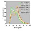
도 3a은 적색/녹색 인광 발광층을 포함한 유기 발광 소자를 나타낸 단면도이며, 도 3b는 도 3a의 구조에 있어서, 녹색 도펀트의 양의 변화에 따라 파장에 따른 휘도를 나타낸 그래프이다.3A is a cross-sectional view illustrating an organic light emitting device including a red / green phosphorescent light emitting layer, and FIG. 3B is a graph showing luminance according to a wavelength according to a change in the amount of green dopants in the structure of FIG. 3A.
즉, 3a의 구조는 도 2의 제 2 스택에 상당한 구성으로, 발광층(EML)이 하나의 호스트에 인광 적색 도펀트와 녹색 노펀트가 포함되어 발광층을 이루는 구조이며, 도 3b는 이 때, 동일 적색 도펀트 농도 대비 녹색 도펀트에 따른 스펙트럼을 나타낸다.That is, the structure of 3a corresponds to the second stack of FIG. 2, in which the light emitting layer EML includes a phosphorescent red dopant and a green nopant in one host to form a light emitting layer, and FIG. It shows the spectrum according to the green dopant relative to the dopant concentration.
도 3b 및 표 1과 같이, 녹색 호스트에 적색 인광 도펀트를 0.4%를 넣은 상태에서, 녹색 인광 도펀트의 첨가량을 5%, 10%, 20%로 하였을 때, 구동 전압(V), 광도 (cd/A), 외부 양자 효율(EQE(%)) 및 CIE 좌표계를 측정한 값을 나타낸 것이다.3B and Table 1, when the red phosphorescent dopant is 0.4% in the green host, the driving voltage (V) and the brightness (cd / A), the external quantum efficiency (EQE (%)) and the measured value of the CIE coordinate system are shown.
예를 들어, 녹색 호스트의 양과 적색 인광 도펀트를 0.4%로 고정하였을 때, 녹색 인광 도펀트의 첨가량을 5%, 10%로 하였을 때는 구동 전압이 3.6V였고, 20%로 하였을 때는 구동 전압이 3.7V로, 녹색 인광 도펀트의 첨가량이 늘었을 때, 구동 전압이 증가하는 경향을 보이고 있다.For example, when the amount of the green host and the red phosphorescent dopant were fixed at 0.4%, the driving voltage was 3.6V when the addition amount of the green phosphorescent dopant was 5% and 10%, and the driving voltage was 3.7V at 20%. As the amount of green phosphorescent dopant added increases, the driving voltage tends to increase.
그런데, 광도(cd/A)와 외부 양자 효율(EQE)는 모두 녹색 인광 도펀트가 10%일 때, 최고 값을 나타내는 것으로, 상기 녹색 인광 도펀트를 10%로 유지하였을 때, 구동 전압을 늘리지 않으며 최적의 광도와 양자효율을 갖는 것을 확인할 수 있었다.However, the luminance (cd / A) and the external quantum efficiency (EQE) are the highest values when the green phosphorescent dopant is 10%. When the green phosphorescent dopant is maintained at 10%, the driving voltage is not increased and is optimal. It was confirmed that it has the brightness and quantum efficiency of.
특히, 도 3b에서는, 녹색 인광 도펀트의 첨가량이 5%로 하였을 때는, 600nm 부근의 파장대와 530nm 파장 대에서 강도가 상대적으로 큰 특성을 나타내나, 전체적으로 강도가 작아 양자 효율이 크지 않은 문제가 있음을 보여주며, 녹색 인광 도펀트의 첨가량이 20%로 하였을 때에는 600nm 부근의 파장대에는 강도가 높으나 그 나머지 영역대에서는 현격히 강도가 낮아져, 적색/녹색 발광을 수행하기 곤란함을 보여준다.In particular, in FIG. 3B, when the amount of the green phosphorescent dopant added is 5%, the intensity is relatively high in the wavelength band around 600 nm and the 530 nm wavelength band, but there is a problem that the intensity is small and the quantum efficiency is not large. When the addition amount of the green phosphorescent dopant is 20%, the intensity is high in the wavelength band around 600 nm, but the intensity is significantly lower in the remaining region, making it difficult to perform red / green light emission.
따라서, 도 3b 및 표 1 모두 적색/녹색 인광 도펀트가 첨가된 발광층을 포함한 스택 구조에서, 녹색 도펀트가 10%일 때, 구동 전압의 효율이 좋게, 가장 적색/녹색의 광을 적절히 발광함을 알 수 있다.3B and Table 1 thus show that in the stack structure including the light emitting layer to which the red / green phosphorescent dopant is added, when the green dopant is 10%, the driving voltage is efficiently emitted and the red / green light is properly emitted. Can be.

도 4a는 여기자 저지층 및 적색/녹색 인광 발광층을 포함하는 유기 발광 소자를 나타낸 단면도이며, 도 4b는 도 4a의 적색 도펀트 양의 변화에 따른 파장에 따른 휘도를 나타낸 그래프이다.4A is a cross-sectional view illustrating an organic light emitting device including an exciton blocking layer and a red / green phosphorescent light emitting layer, and FIG. 4B is a graph showing luminance according to a wavelength according to a change in the amount of red dopant of FIG. 4A.
도 4a 또한, 적색/녹색 인광 발광층을 포함하는 스택 구조를 나타낸 것으로, 도 4b 및 표 2의 실험에서는 상기 녹색 호스트에 상기 녹색 인광 도펀트를 10%를 첨가하고, 이에 적색 인광 도펀트의 양을 변화시키며 IVL 데이터 및 파장에 따른 강도(Intensity)를 측정한 값들이다. 여기서, 상기 녹색/녹색 인광 발광층과 정공 수송층(HTL)과의 사이에 여기자 저지층(EBL)을 더 구비한 경우도 실험하였다.FIG. 4A also shows a stack structure including a red / green phosphorescent light emitting layer. In the experiments of FIGS. 4B and 2, 10% of the green phosphorescent dopant is added to the green host, and the amount of the red phosphorescent dopant is changed. IVL data and intensity measured according to wavelength are measured. Here, the case where the exciton blocking layer (EBL) was further provided between the green / green phosphorescent layer and the hole transport layer (HTL) was also tested.
즉, 표 2에서는, 여기자 저지층을 갖지 않은 구조에서, 적색 인광 도펀트를 0.1%에서 차례로 0.1% 씩 0.4% 까지 첨가하여 실험하였을 때, 구동 전압은 적색 인광 도펀트의 첨가량이 늘어난 만큼 증가하는 점을 보여주나, 양자 효율은 반드시 구동 전압의 증가에 따라 늘어나는 점은 나타내지 못함을 나타낸다.That is, in Table 2, in a structure without an exciton blocking layer, when the red phosphorescent dopant was tested by adding 0.1% to 0.4% by 0.1% in turn, the driving voltage increased as the amount of red phosphorescent dopant increased. It is shown that the quantum efficiency does not necessarily increase as the driving voltage increases.
오히려, 여기자 저지층을 포함하였을 때, 여기자 저지층이 없는 구조에서, 가장 낮은 양자 효율을 갖는 적색 인광 도펀트를 0.2%를 포함한 경우에, 구동 전압이 3.8V에 양자 효율이 19.4%로 급격히 증가함을 보여주고 있으며, 이 경우, 상대적으로 여기자 저지층이 없는 구조 대비 광효율이 좋음을 알 수 있다.Rather, when the exciton blocking layer is included, in the structure without the exciton blocking layer, when the red phosphorescent dopant having the lowest quantum efficiency is included 0.2%, the quantum efficiency rapidly increases to 9.4V and 19.4%. In this case, it can be seen that the light efficiency is good in comparison with the structure without the exciton blocking layer in this case.
도 4b의 그래프의 흰색으로 표시된 여기자 저지층(삼중항 저지층: triplet blocking layer)부분과 같이, 600nm 파장대와 530 nm 파장대에서 고른 강도를 가짐을 알 수 있다.Like the exciton blocking layer (triple blocking layer) shown in white in the graph of FIG. 4B, it has a uniform intensity in the 600 nm wavelength band and the 530 nm wavelength band.

그런데, 여기자 저지층을 포함할 경우, 수명이 저하되는 문제가 있으므로, 광도 및 양자 효율 등의 특성을 개선하는 데 있어서, 여기자 저지층 외에 다른 각도에서 특성을 개선하는 점에 대해 고려한다.By the way, when the exciton blocking layer is included, there is a problem that the service life is reduced. Therefore, in improving the characteristics such as brightness and quantum efficiency, consideration is given to the improvement of the characteristics at an angle other than the exciton blocking layer.
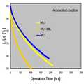
도 5a는 적색/녹색 인광 발광층을 포함하는 유기 발광 소자의 적층 구조를 나타낸 다이어그램이며, 도 5b는 적색/녹색 인광 발광층의 수명을 나타낸 그래프이다.FIG. 5A is a diagram illustrating a laminated structure of an organic light emitting device including a red / green phosphorescent light emitting layer, and FIG. 5B is a graph showing the life of a red / green phosphorescent light emitting layer.
도 5a와 같이, 적색/녹색 인광 발광층을 포함하는 스택 구조는, 양쪽의 음양극(Anode)과 음극(Cathode) 사이에, 차례로, 제 1 정공 수송층(HTL1) 적색/녹색 인광 발광층, 전자 수송층(ETL)을 포함하여 이루어진다. 이 때, 제 1 정공 수송층은 경우에 따라, 상기 제 1 정공 수송층은 여기 상태 에너지가 발광층의 값보다 낮거나 동일한 경우이다.As shown in FIG. 5A, a stack structure including a red / green phosphorescent light emitting layer may include a first hole transport layer HTL1 red / green phosphorescent light emitting layer and an electron transporting layer between both anodes and cathodes. ETL). In this case, the first hole transport layer may be a case where the first hole transport layer has an excitation state energy lower than or equal to a value of the light emitting layer.
경우에 따라, 상기 제 1 정공 수송층과 적색/녹색 인광 발광층 사이에 여기자 저지층을 더 구비할 수도 있으며, 혹은 상기 제 1 정공 수송층을 적색/녹색 인광 발광층의 여기 상태 에너지보다 0.01~0.4eV 높은 값을 갖는 제 2 정공 수송층으로 대체할 수 있다.In some cases, an exciton blocking layer may be further provided between the first hole transport layer and the red / green phosphorescent layer, or the first hole transport layer is 0.01 to 0.4 eV higher than the excited state energy of the red / green phosphorescent layer. It can be replaced with a second hole transport layer having a.
도 5b의 그래프는, 도 5a의 각각의 예의 수명을 나타낸 것으로, 여기자 저지층을 사용하였을 때, 수명이 낮음을 알 수 있다. 이와 달리, 제 1 정공 수송층이나 제 2 정공 수송층의 단일층으로 구비한 경우에는 여기자 저지층을 사용한 예에 비해 2배 정도 수명이 개선됨을 알 수 있다.The graph of FIG. 5B shows the lifetime of each example of FIG. 5A, and it can be seen that the lifetime is low when the exciton blocking layer is used. On the other hand, when the single hole transport layer or the second hole transport layer is provided as a single layer it can be seen that the life is improved by about twice as compared to the example using the exciton blocking layer.
그러나, 표 3과 같이, 제 1 정공 수송층을 구비한 경우에는 여기자 저지층을 구비한 경우에 비해, 양자 효율이나 광도가 현저히 떨어져 수명만을 보고 제 1 정공 수송층만을 이용하기는 곤란하다. 상대적으로 제 2 정공 수송층을 이용한 경우, 제 1 정공 수송층만을 구비한 경우에 비해 양자효율과 광도가 모두 개선된 점을 확인할 수 있었다.However, as shown in Table 3, when the first hole transporting layer is provided, it is difficult to use only the first hole transporting layer in view of the lifetime since the quantum efficiency and luminous intensity are considerably lower than those in the case where the exciton blocking layer is provided. In the case of using the second hole transport layer, it was confirmed that both the quantum efficiency and the brightness were improved as compared with the case where only the first hole transport layer was provided.
따라서, 수명 및 휘도와 양자 효율이 모두 좋은 특성을 고려하여 제 2 정공 수송층을 이용하는 것이 바람직하다.Therefore, it is preferable to use the second hole transporting layer in consideration of the characteristics of both the lifespan, the brightness and the quantum efficiency.

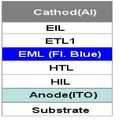
도 6a 및 도 6b는 청색 형광 발광층을 포함하는 유기 발광 소자를 나타낸 적층 구조를 다른 형태로 나타낸 예를 도시한 단면도이다. 그리고, 도 7은 전자수송 촉매층의 농도에 따른 IVL 데이터를 나타낸 그래프이다. 또한, 도 8은 도 6a 및 도 6b의 구조에 있어서, 각각 Li 또는 LiF의 농도를 달리했을 때의 수명을 나타낸 그래프이다.6A and 6B are cross-sectional views illustrating examples in which a stacked structure of an organic light emitting device including a blue fluorescent light emitting layer is shown in another form. And, Figure 7 is a graph showing the IVL data according to the concentration of the electron transport catalyst layer. 8 is a graph showing the life when the concentration of Li or LiF is different in the structures of FIGS. 6A and 6B, respectively.
도 6a는 청색 형광 발광층을 포함한 스택 구조에 있어서, 전자 수송층(ETL)을 단일층으로 나타낸 것이며, 도 6b는 전자 수송층에 금속(Li과 같은 알칼리 금속)을 도핑한 전자 수송 촉매층(Li(x%))을 더 포함하여 이중층으로 구성한 예를 나타낸다.FIG. 6A illustrates an electron transport layer (ETL) as a single layer in a stack structure including a blue fluorescent light emitting layer, and FIG. 6B illustrates an electron transport catalyst layer (Li (x%) in which an electron transport layer is doped with a metal (alkali metal such as Li). The example which consists of a double layer further including)) is shown.
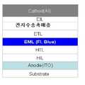
여기서, 상기 청색 형광 발광층(EML:Fl. Blue)의 하측에는 기판(Substrate), 양극(Anode)(ITO), 정공 주입층(HIL), 정공 수송층(HTL)이 공통적으로 적층되어 이루어진다.Here, a substrate, an anode (ITO), a hole injection layer (HIL), and a hole transport layer (HTL) are commonly stacked below the blue fluorescent light emitting layer (EML: Fl.Blue).
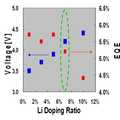
표 4 및 도 7과 같이, 도 6b의 이중층의 경우, Li의 도핑량이 증가하였을 때, 구동 전압이 증가하였음을 보여주나, 양자 효율은 7%의 성분비로 경계로 떨어짐을 알 수 있다.As shown in Table 4 and FIG. 7, in the case of the double layer of FIG. 6B, when the doping amount of Li is increased, it shows that the driving voltage is increased, but it can be seen that the quantum efficiency drops to the boundary with a component ratio of 7%.
그러나, 도 8과 같이, Li의 도핑량이 증가하게 되면, 양자 효율을 떨어지나, 상대적으로 그 수명은 늘어나는 점을 확인할 수 있었으며, 양자 효율과 수명 모두를 고려하여, 상기 전자 수송 촉매층의 Li 도핑량이 약 7% 일 때, 최적의 양자 효율 5.2%이 수명이 나옴을 알 수 있다.However, as shown in FIG. 8, when the doping amount of Li is increased, the quantum efficiency is decreased, but the lifetime thereof is relatively increased. In consideration of both the quantum efficiency and the lifetime, the Li doping amount of the electron transporting catalyst layer is weak. At 7%, it can be seen that 5.2% of the optimal quantum efficiency comes to life.

도 9a 및 도 9b는 청색 형광 발광층을 포함하는 유기 발광 소자에 있어서, 전자 수송층(ETL)을 단일로 구비한 경우와, 전자수송층(ETL)과 전자 수송 촉매층을 적층하여 구비한 구조를 각각 나타낸 단면도이다.9A and 9B are cross-sectional views each illustrating a structure in which an electron transport layer (ETL) is provided as a single layer and an electron transport layer (ETL) and an electron transport catalyst layer are stacked in an organic light emitting device including a blue fluorescent light emitting layer. to be.
청색형광 발광층을 포함하는 스택 구조에 있어서, 도 9a와 같이, 단일 전자 수송층(ETL)을 구비한 경우와 도 9b와 같이, 전자 수송층(ETL)/전자 수송 촉매층의 적층체를 구비한 구조를 비교하면, 표 5와 같이, 전하 원자가(charge valence)와 TTA(Triplet-Triplet Annihilation: 삼중항 쌍 소멸) 형성을 위해 삼중항 에너지 높은 전자수송층(ETL) 및 정공 수송층(HTL)을 청색 형광 발광층(EML(Fl. Blue))의 계면에 적용하였으며, 전자 이동도가 좋은 전자수송 촉매층을 상기 전자수송층(ETL) 위에 바로 적층시켜 구비하였다. 이 경우, 상기 전자 수송층(ETL)/전자수송 촉매층의 적층 구조에서 가장 좋은 IVL 특성을 나타낸다.In the stack structure including the blue fluorescence emitting layer, as shown in FIG. 9A, a structure including a laminate of an electron transport layer (ETL) / electron transport catalyst layer is compared with a case where a single electron transport layer (ETL) is provided as in FIG. 9B. When the electron transport layer (ETL) and the hole transport layer (HTL) have high triplet energy to form charge valence and triplet pair annihilation (TTA), as shown in Table 5, the blue fluorescent layer (EML) (Fl. Blue)) was applied to the interface, the electron transport catalyst layer having a good electron mobility was provided by directly stacked on the electron transport layer (ETL). In this case, the best IVL characteristics are shown in the laminated structure of the electron transport layer (ETL) / electron transport catalyst layer.
즉, 표 5와 같이, 상기 전자 수송층과 전자수송 촉매층을 두께를 달리하여 실험한 결과, 각각 150Å/ 150Å의 두께로 적층하였을 때, 가장 양자 효율이 9.7%로 높고, 광도도 9.3cd/A로높으며, 상대적으로 구동 전압도 낮은 값을 나타냄을 확인할 수 있다.That is, as shown in Table 5, when the electron transport layer and the electron transport catalyst layer was tested by varying the thickness, when laminated at a thickness of 150 Å / 150 각각 each, the quantum efficiency is the highest as 9.7%, the brightness is 9.3 cd / A It can be seen that the driving voltage is high and the driving voltage is relatively low.
도 10은 본 발명의 백색 발광 소자에 있어서, 단일 전자 수송층을 구비한 경우와, 전자수송층/전자수송 촉매층을 적층한 구조의 경우 파장에 따른 스펙트럼을 나타낸 그래프이다. 또한, 도 11은 본 발명의 백색 발광 소자에 있어서, 단일 전자 수송층을 구비한 경우와, 전자수송층/전자수송 촉매층을 적층한 구조의 경우, 수명을 나타낸 그래프이다.FIG. 10 is a graph showing the spectrum according to the wavelength of the white light emitting device of the present invention in the case of having a single electron transporting layer and a structure in which an electron transporting layer / electron transporting catalyst layer is laminated. FIG. 11 is a graph showing the lifespan of the white light emitting device of the present invention in the case where a single electron transport layer is provided and in the case where the electron transport layer / electron transport catalyst layer is laminated.
금속이 도핑된 전자수송 촉매층 및 전자 수송층의 적층 구조와, 높은 삼중항 에너지를 갖는 정공 수송층 및 전자 수송층을 적용하여 2 스택 구조의 백색 유기 발광 소자를 제작하였으며, 이 때의 스펙트럼 및 IVL 데이터가 도 10과 표 6의 Device 2로 표현된 그래프이다.The stacked structure of the metal-doped electron transporting catalyst layer and the electron transporting layer, the hole transporting layer and the electron transporting layer having high triplet energy were applied, and a white organic light emitting device having a 2 stack structure was fabricated. This is a graph represented by
여기서, 도 10의 그래프에서, 파란색으로 표현된 Device A2의 경우, 청색 파장인 약 450~500nm의 범위에서, 강도가 커져 효율이 개선됨을 보이고 있으며, 이는 2 스택 구조에서, 상대적으로 적색/녹색 인광 발광층에 비해 효율이 떨어지는 청색 형광층의 효율을 향상시킨 점을 의미한다.Here, in the graph of FIG. 10, in the case of Device A2 represented in blue, the intensity is increased in the range of about 450 nm to 500 nm, which is a blue wavelength, and the efficiency is improved. This means that the efficiency of the blue fluorescent layer, which is less efficient than the light emitting layer, is improved.
표 6에서는, Device A2에서는 구동 전압이 증가하였으나, 광도나 전류 값은 약간 낮은 값을 나타내며, 색좌표계는 색온도를 높이는 효과가 있었음을 나타낸다.In Table 6, the driving voltage was increased in Device A2, but the luminance and current values were slightly lower, and the color coordinate system had an effect of increasing the color temperature.

도 11과 같이, 상기 Device A2의 수명이 Device A1의 수명에 비해 2배 이상 향상된 것을 확인할 수 있었다.As shown in FIG. 11, the lifespan of the device A2 was confirmed to be more than two times improved compared to the lifespan of the device A1.
도 12는 본 발명의 백색 발광 소자에 있어서, 컬러 필터층을 적용한 경우에 따른 파장에 따른 휘도를 나타낸 그래프이다.12 is a graph showing luminance according to a wavelength when a color filter layer is applied in the white light emitting device of the present invention.
도 12는 컬러 필터 R, G, B 필름의 각각의 스펙트럼과 Device A1과 Device A2의 스펙트럼을 오버랩하여 나타낸 것이며, 표 7은 개선된 본 발명의 Device A2의 구조에서 향상된 형광 효율로 인하여 소비전력이 개선된 점을 나타낸다.FIG. 12 shows overlapping spectra of color filters R, G, and B films and spectra of Device A1 and Device A2. Table 7 shows power consumption due to improved fluorescence efficiency in the structure of Device A2 of the present invention. It shows an improvement.
즉, 표 7을 살펴보면, Device A1과 Device A2를 비교하였을 때, Device A2에서 적색 광도가 낮아지고, 청색 광도가 현저히 향상된 것을 보여주며, 특히 소비전력을 살펴보면, 52W에서 37.4W로 2/3 수준으로 줄어듦을 확인할 수 있다.That is, Table 7 shows that when comparing Device A1 and Device A2, the red luminous intensity is lowered and the blue luminous intensity is remarkably improved in Device A2. Especially, the power consumption is 2/3 level from 52W to 37.4W. You can see the shrinkage.

한편, 백색 유기 발광 소자는 색 순도, 색 안정성, 전류 및 전압에 따른 색 안정성 등의 광 특성과, 발광 효율, 수명, 제조의 용이성 등이 중요하기 때문에 다양한 방식이 개발 진행 중에 있다. 최근에는 인광과 형광을 조합하여 일중항 여기 상태와 삼중항 여기 상태를 모두 이용하여 내부 양자효율을 높이는 방식의 소자 구조가 개발되고 있다.Meanwhile, various methods are being developed for the white organic light emitting diode because the optical properties such as color purity, color stability, color stability according to current and voltage, luminous efficiency, lifetime, and ease of manufacture are important. Recently, a device structure of a method of increasing internal quantum efficiency by using both a singlet excited state and a triplet excited state by combining phosphorescence and fluorescence has been developed.
또한, 적, 녹, 청색을 모두 인광으로 적용하여 내부 양자 효율(IQE: Internal Quantum Efficiency) 100%를 얻을 수 있는 고효율의 백색 유기 발광 소자도 개발된 상태이다.In addition, a high-efficiency white organic light emitting device that can obtain 100% of internal quantum efficiency (IQE) by applying red, green, and blue as phosphorescent light has also been developed.
그러나, 아직까지 수명면에서 많은 개선이 필요한 청색 인광 재료로 인하여, 청색 형광과 적색, 녹색 인광을 이용한 2 스택 백색 유기 발광 소자가 주로 개발되고 있다.However, due to the blue phosphor material which still needs much improvement in terms of lifespan, a two-stacked white organic light emitting device using blue fluorescence, red phosphorus and green phosphorescence has been mainly developed.
그런데, 청색 형광의 제한적인 효율로 인한 수명 문제로 인하여 소비 전력이 높아지는 문제로 인해 대형 디스플레이 적용에 한계로 지적되어 왔다.However, it has been pointed out as a limitation in the application of a large display due to the problem that the power consumption is increased due to the lifetime problem due to the limited efficiency of the blue fluorescence.
본 발명의 유기 발광 소자는 높은 삼중항 에너지를 갖는 정공층과 금속 도핑된 전자 수송 촉매층을 전자 수송층에 부가하여 삼중항 쌍 소멸(triplet-triplet annihilation)을 이용하여 청색 형광의 효율을 높이고 수명을 증가시켜 색감 및 저소비전력을 꾀할 수 있다The organic light emitting device according to the present invention adds a hole layer having a high triplet energy and a metal doped electron transport catalyst layer to the electron transport layer to increase efficiency and increase lifetime of blue fluorescence using triplet-triplet annihilation. Color and low power consumption
한편, 이상에서 설명한 본 발명은 상술한 실시예 및 첨부된 도면에 한정되는 것이 아니고, 본 발명의 기술적 사상을 벗어나지 않는 범위내에서 여러 가지 치환, 변형 및 변경이 가능하다는 것이 본 발명이 속하는 기술분야에서 통상의 지식을 가진 자에게 있어 명백할 것이다.While the present invention has been described in connection with what is presently considered to be the most practical and preferred embodiment, it is to be understood that the invention is not limited to the disclosed embodiments, but, on the contrary, is intended to cover various modifications and equivalent arrangements included within the spirit and scope of the appended claims. Will be apparent to those of ordinary skill in the art.
도 1은 본 발명의 백색 유기 발광 소자의 일예를 나타낸 단면도1 is a cross-sectional view showing an example of a white organic light-emitting device of the present invention
도 2는 도 1의 수명을 개선한 본 발명의 백색 유기 발광 소자의 다른 실시예를 나타낸 단면도2 is a cross-sectional view showing another embodiment of the white organic light emitting diode of the present invention having an improved lifetime of FIG. 1.
도 3a은 적색/녹색 인광 발광층을 포함한 유기 발광 소자를 나타낸 단면도3A is a cross-sectional view showing an organic light emitting device including a red / green phosphorescent light emitting layer
도 3b는 도 3a의 구조에 있어서, 녹색 도펀트의 양의 변화에 따라 파장에 따른 휘도를 나타낸 그래프3B is a graph showing luminance according to a wavelength according to a change of the amount of the green dopant in the structure of FIG. 3A.
도 4a는 여기자 저지층 및 적색/녹색 인광 발광층을 포함하는 유기 발광 소자를 나타낸 단면도4A is a cross-sectional view of an organic light emitting device including an exciton blocking layer and a red / green phosphorescent light emitting layer
도 4b는 도 4a의 적색 도펀트 양의 변화에 따른 파장에 따른 휘도를 나타낸 그래프FIG. 4B is a graph showing luminance according to wavelength according to the change of the amount of red dopant of FIG. 4A.
도 5a는 적색/녹색 인광 발광층을 포함하는 유기 발광 소자의 적층 구조를 나타낸 다이어그램5A is a diagram illustrating a laminated structure of an organic light emitting device including a red / green phosphorescent layer
도 5b는 적색/녹색 인광 발광층의 수명을 나타낸 그래프5B is a graph showing the lifetime of a red / green phosphorescent layer
도 6a 및 도 6b는 청색 형광 발광층을 포함하는 유기 발광 소자를 나타낸 적층 구조를 다른 형태로 나타낸 예를 도시한 단면도6A and 6B are cross-sectional views illustrating examples in which the stacked structure of the organic light emitting device including the blue fluorescent light emitting layer is shown in another form.
도 7은 전자수송 촉매층의 농도에 따른 IVL 데이터를 나타낸 그래프7 is a graph showing IVL data according to the concentration of the electron transport catalyst layer
도 8은 도 6a 및 도 6b의 구조에 있어서, 각각 Li 또는 LiF의 농도를 달리했을 때의 수명을 나타낸 그래프FIG. 8 is a graph showing the lifespan at the concentration of Li or LiF in the structures of FIGS. 6A and 6B, respectively.
도 9a 및 도 9b는 청색 형광 발광층을 포함하는 유기 발광 소자에 있어서, 전자 수송층을 단일로 구비한 경우와, 전자수송층과 전자 수송 촉매층을 적층하여 구비한 구조를 각각 나타낸 단면도9A and 9B are cross-sectional views each illustrating a structure in which an electron transport layer is provided and a structure in which an electron transport layer and an electron transport catalyst layer are stacked in the organic light emitting device including a blue fluorescent light emitting layer.
도 10은 본 발명의 백색 발광 소자에 있어서, 단일 전자 수송층을 구비한 경우와, 전자수송층/전자수송 촉매층을 적층한 구조의 경우 파장에 따른 스펙트럼을 나타낸 그래프10 is a graph showing the spectrum according to the wavelength of the white light emitting device of the present invention, in the case of having a single electron transporting layer and in a structure in which an electron transporting layer / electron transporting catalyst layer is laminated.
도 11은 본 발명의 백색 발광 소자에 있어서, 단일 전자 수송층을 구비한 경우와, 전자수송층/전자수송 촉매층을 적층한 구조의 경우, 수명을 나타낸 그래프FIG. 11 is a graph showing the lifespan of the white light emitting device according to the present invention in the case where a single electron transport layer is provided and in a structure in which an electron transport layer / electron transport catalyst layer is laminated.
도 12는 본 발명의 백색 발광 소자에 있어서, 컬러 필터층을 적용한 경우에 따른 파장에 따른 휘도를 나타낸 그래프12 is a graph showing luminance according to a wavelength when a color filter layer is applied in a white light emitting device of the present invention;
*도면의 주요 부분에 따른 부호의 설명** Description of the symbols according to the main parts of the drawings *
300: 기판 301: 양극300: substrate 301: anode
303: 제 1 정공 주입층 305: 제 1 정공 전달층303: first hole injection layer 305: first hole transport layer
310: 제 1 발광층 315: 제 1 전자수송층310: first light emitting layer 315: first electron transport layer
320: 전자 수송 촉매층 323: 전하 생성층320: electron transport catalyst layer 323: charge generating layer
325: 제 2 정공 수송층 330: 제 2 발광층325: second hole transport layer 330: second emission layer
333: 제 2 전자 수송층 336: 전자주입층333: second electron transport layer 336: electron injection layer
340: 음극340: cathode
Claims (9)
Translated fromKoreanPriority Applications (3)
| Application Number | Priority Date | Filing Date | Title |
|---|---|---|---|
| KR1020090092596AKR101351410B1 (en) | 2009-09-29 | 2009-09-29 | White Organic Light Emitting Device |
| CN2010102362761ACN102034934B (en) | 2009-09-29 | 2010-07-21 | White organic light emitting device |
| US12/856,050US8350257B2 (en) | 2009-09-29 | 2010-08-13 | White organic light emitting device |
Applications Claiming Priority (1)
| Application Number | Priority Date | Filing Date | Title |
|---|---|---|---|
| KR1020090092596AKR101351410B1 (en) | 2009-09-29 | 2009-09-29 | White Organic Light Emitting Device |
Publications (2)
| Publication Number | Publication Date |
|---|---|
| KR20110035048A KR20110035048A (en) | 2011-04-06 |
| KR101351410B1true KR101351410B1 (en) | 2014-01-14 |
Family
ID=43779288
Family Applications (1)
| Application Number | Title | Priority Date | Filing Date |
|---|---|---|---|
| KR1020090092596AActiveKR101351410B1 (en) | 2009-09-29 | 2009-09-29 | White Organic Light Emitting Device |
Country Status (3)
| Country | Link |
|---|---|
| US (1) | US8350257B2 (en) |
| KR (1) | KR101351410B1 (en) |
| CN (1) | CN102034934B (en) |
Cited By (2)
| Publication number | Priority date | Publication date | Assignee | Title |
|---|---|---|---|---|
| KR20180025049A (en) | 2016-08-31 | 2018-03-08 | 엘지디스플레이 주식회사 | Organic light emitting device and organic light emitting display device comprising the same |
| US12207516B2 (en) | 2020-02-14 | 2025-01-21 | Samsung Display Co., Ltd. | Organic light-emitting display device |
Families Citing this family (75)
| Publication number | Priority date | Publication date | Assignee | Title |
|---|---|---|---|---|
| WO2012063171A1 (en)* | 2010-11-09 | 2012-05-18 | Koninklijke Philips Electronics N.V. | Organic electroluminescent device |
| DE112012001504B4 (en)* | 2011-03-30 | 2017-09-21 | Semiconductor Energy Laboratory Co., Ltd. | Light-emitting element |
| TWI505524B (en)* | 2011-05-20 | 2015-10-21 | Au Optronics Corp | Organic electroluminescent light source |
| KR101429537B1 (en)* | 2011-07-11 | 2014-08-12 | 엘지디스플레이 주식회사 | Organic light emitting diodes |
| CN103022370B (en) | 2011-09-20 | 2016-02-03 | 乐金显示有限公司 | White organic light emitting device |
| KR101469484B1 (en)* | 2011-09-20 | 2014-12-05 | 엘지디스플레이 주식회사 | White Organic Light Emitting Device |
| KR101419249B1 (en)* | 2011-10-12 | 2014-07-17 | 엘지디스플레이 주식회사 | White Organic Light Emitting Device |
| US8884274B2 (en)* | 2011-10-12 | 2014-11-11 | Lg Display Co., Ltd. | White organic light emitting device |
| KR101511552B1 (en)* | 2011-11-10 | 2015-04-13 | 엘지디스플레이 주식회사 | White Organic Emitting Device and Display Device Using the Same |
| CN103107288B (en)* | 2011-11-10 | 2016-02-03 | 乐金显示有限公司 | The display unit of white organic light emitting device and use white organic light emitting device |
| CN103137877B (en)* | 2011-11-28 | 2016-09-07 | 海洋王照明科技股份有限公司 | Electroluminescent device and preparation method thereof |
| KR101429924B1 (en)* | 2011-12-08 | 2014-08-14 | 엘지디스플레이 주식회사 | Tandem White Organic Emitting Device |
| TW201328421A (en)* | 2011-12-19 | 2013-07-01 | Au Optronics Corp | Organic electroluminescent apparatus |
| KR102009804B1 (en)* | 2011-12-26 | 2019-08-13 | 엘지디스플레이 주식회사 | Organic light emitting diode display device and method for manufacturing the same |
| KR101908509B1 (en)* | 2012-04-05 | 2018-10-18 | 엘지디스플레이 주식회사 | Tandem White Organic Emitting Device |
| KR101908510B1 (en)* | 2012-04-06 | 2018-10-17 | 엘지디스플레이 주식회사 | White Organic Emitting Device and Display Device Using the Same |
| CN102779948B (en)* | 2012-07-31 | 2016-03-02 | 京东方科技集团股份有限公司 | White color organic electroluminescence device and manufacture method thereof |
| CN103681760B (en)* | 2012-09-12 | 2016-08-17 | 乐金显示有限公司 | Organic light-emitting display device |
| TWI569491B (en)* | 2012-10-11 | 2017-02-01 | Joled Inc | Organic EL display device and manufacturing method thereof, ink and electronic machine |
| GB2508289B (en)* | 2012-10-31 | 2015-09-30 | Lg Display Co Ltd | Organic light emitting display device |
| CN103915470B (en)* | 2012-12-31 | 2016-12-07 | 乐金显示有限公司 | Organic light-emitting display device |
| CN104064680A (en)* | 2013-03-21 | 2014-09-24 | 海洋王照明科技股份有限公司 | Organic electroluminescent device and preparation method thereof |
| KR102059601B1 (en) | 2013-04-01 | 2019-12-27 | 삼성디스플레이 주식회사 | Organic light emitting diode device |
| JP6556694B2 (en)* | 2013-04-08 | 2019-08-07 | メルク パテント ゲーエムベーハー | Organic light emitting device having delayed fluorescence |
| KR102081123B1 (en)* | 2013-10-02 | 2020-02-26 | 엘지디스플레이 주식회사 | Organic light emitting display |
| KR102088883B1 (en)* | 2013-12-02 | 2020-03-16 | 엘지디스플레이 주식회사 | Organic Light Emitting Display Device |
| KR102101202B1 (en)* | 2013-12-30 | 2020-04-17 | 엘지디스플레이 주식회사 | Organic Light Emitting Diode And Organic Light Emitting Diode Display Device Including The Same |
| KR102203774B1 (en)* | 2013-12-31 | 2021-01-18 | 엘지디스플레이 주식회사 | White Organic Emitting Device |
| DE102014102191B4 (en)* | 2014-02-20 | 2017-12-28 | Osram Oled Gmbh | Organic light emitting device with improved color rendering index |
| TW201537800A (en)* | 2014-03-26 | 2015-10-01 | Chunghwa Picture Tubes Ltd | Organic light-emitting diode |
| KR102145759B1 (en)* | 2014-03-27 | 2020-08-20 | 엘지디스플레이 주식회사 | Organic Light Emitting Device |
| US9685622B2 (en) | 2014-03-31 | 2017-06-20 | Lg Display Co., Ltd. | White organic light emitting device |
| KR102151412B1 (en)* | 2014-03-31 | 2020-10-27 | 엘지디스플레이 주식회사 | White organic light emitting device |
| KR102165234B1 (en)* | 2014-04-25 | 2020-10-14 | 엘지디스플레이 주식회사 | White organic light emitting device |
| KR102279513B1 (en)* | 2014-04-29 | 2021-07-19 | 엘지디스플레이 주식회사 | White organic light emitting device |
| KR102133407B1 (en)* | 2014-04-29 | 2020-07-14 | 엘지디스플레이 주식회사 | White organic light emitting device |
| EP2950362B1 (en) | 2014-05-26 | 2021-03-24 | LG Display Co., Ltd. | White organic light emitting device |
| CN104143607B (en)* | 2014-07-03 | 2017-06-09 | 重庆师范大学 | A kind of laminated organic electroluminescent device and articulamentum |
| EP3016159B1 (en) | 2014-10-27 | 2021-12-08 | LG Display Co., Ltd. | White organic light emitting device |
| EP3016160B1 (en) | 2014-10-28 | 2020-01-08 | LG Display Co., Ltd. | White organic light emitting diode and organic light emitting display device using the same |
| EP3309853B1 (en) | 2014-12-08 | 2019-03-13 | LG Display Co., Ltd. | Organic light emitting display device |
| KR102381626B1 (en) | 2014-12-17 | 2022-04-01 | 엘지디스플레이 주식회사 | Organic light emitting display device |
| WO2016111534A1 (en)* | 2015-01-05 | 2016-07-14 | 코닝정밀소재 주식회사 | Tandem type organic light emitting device |
| KR101759294B1 (en) | 2015-01-05 | 2017-07-18 | 코닝정밀소재 주식회사 | Tandem type organic light emitting device |
| WO2016111535A1 (en)* | 2015-01-05 | 2016-07-14 | 코닝정밀소재 주식회사 | Tandem organic light-emitting element |
| CN104576702B (en)* | 2015-01-21 | 2017-10-13 | 深圳市华星光电技术有限公司 | OLED chromatic displays |
| KR102435038B1 (en)* | 2015-03-30 | 2022-08-22 | 엘지디스플레이 주식회사 | Organic light emitting display device |
| KR102331042B1 (en)* | 2015-08-31 | 2021-11-24 | 엘지디스플레이 주식회사 | Organic light emitting device |
| KR102357869B1 (en) | 2015-09-11 | 2022-01-28 | 엘지디스플레이 주식회사 | Organic light emitting display device and lighting apparatus for vehicles using the same |
| KR102389833B1 (en) | 2015-10-23 | 2022-04-21 | 엘지디스플레이 주식회사 | Organic light emitting display device |
| KR102377466B1 (en)* | 2015-10-29 | 2022-03-21 | 엘지디스플레이 주식회사 | Organic light emitting display apparatus |
| US10374183B2 (en) | 2015-11-19 | 2019-08-06 | Lg Display Co., Ltd. | Organic light emitting display device having layer to control charge transfer |
| KR102574052B1 (en) | 2015-11-19 | 2023-09-04 | 엘지디스플레이 주식회사 | Organic light emitting display device |
| KR102431636B1 (en) | 2015-11-26 | 2022-08-10 | 엘지디스플레이 주식회사 | Organic light emitting display device |
| KR102463519B1 (en) | 2015-12-17 | 2022-11-03 | 엘지디스플레이 주식회사 | Organic light emitting display device |
| KR102490381B1 (en) | 2015-12-24 | 2023-01-18 | 엘지디스플레이 주식회사 | Organic light emitting display device and organic light emitting stacked structure |
| KR102520026B1 (en) | 2015-12-30 | 2023-04-07 | 엘지디스플레이 주식회사 | Organic light emitting diode |
| KR102553276B1 (en) | 2016-03-29 | 2023-07-06 | 엘지디스플레이 주식회사 | Organic light emitting display device |
| WO2018058524A1 (en)* | 2016-09-30 | 2018-04-05 | Boe Technology Group Co., Ltd. | Organic light emitting diode, display panel and display apparatus having the same, and fabricating method thereof |
| CN107507922A (en)* | 2017-06-27 | 2017-12-22 | 广东工业大学 | A tandem organic electroluminescent device |
| CN107425129B (en)* | 2017-07-26 | 2019-12-06 | 上海天马有机发光显示技术有限公司 | An organic light-emitting display panel, its color temperature adjustment method and display device |
| WO2019049192A1 (en)* | 2017-09-05 | 2019-03-14 | シャープ株式会社 | Light emitting device, manufacturing method of light emitting device, and manufacturing apparatus of light emitting device |
| CN107611276B (en)* | 2017-09-22 | 2019-03-12 | 京东方科技集团股份有限公司 | Organic Light Emitting Diode and display panel |
| KR102476814B1 (en)* | 2017-12-12 | 2022-12-12 | 엘지디스플레이 주식회사 | Illumination Device |
| KR102529109B1 (en)* | 2018-08-07 | 2023-05-03 | 엘지디스플레이 주식회사 | Light emitting diode and electroluminescent display device including the same |
| US12108671B2 (en)* | 2019-11-01 | 2024-10-01 | Duk San Neolux Co., Ltd. | Organic electric element comprising a plurality of emission-auxiliary layers and electronic device comprising it |
| JP7316385B2 (en)* | 2020-01-15 | 2023-07-27 | シャープ株式会社 | light-emitting element, light-emitting device |
| CN111524463B (en)* | 2020-05-29 | 2023-04-21 | 京东方科技集团股份有限公司 | Display panel, manufacturing method thereof, and display device |
| CN114256428B (en)* | 2020-09-23 | 2025-02-07 | 北京小米移动软件有限公司 | Display panel and display device |
| KR20220097056A (en)* | 2020-12-31 | 2022-07-07 | 엘지디스플레이 주식회사 | White Light Emitting Device and Light Emitting Display Device Using the Same |
| CN112909053A (en)* | 2021-01-26 | 2021-06-04 | 京东方科技集团股份有限公司 | Display device, display panel and manufacturing method thereof |
| CN114122087B (en)* | 2021-11-12 | 2024-08-23 | 昆山工研院新型平板显示技术中心有限公司 | Display panel and manufacturing method thereof |
| CN114792765A (en)* | 2022-04-26 | 2022-07-26 | 云谷(固安)科技有限公司 | Light-emitting unit, display module, display panel and electronic equipment |
| CN115207239A (en)* | 2022-07-01 | 2022-10-18 | 武汉华星光电半导体显示技术有限公司 | A display panel and display device |
| CN117460275A (en)* | 2023-07-31 | 2024-01-26 | 武汉华星光电半导体显示技术有限公司 | Display panel |
Citations (1)
| Publication number | Priority date | Publication date | Assignee | Title |
|---|---|---|---|---|
| US7994498B2 (en)* | 2008-12-01 | 2011-08-09 | Lg Display Co., Ltd. | White organic light emitting device and method for manufacturing the same |
Family Cites Families (6)
| Publication number | Priority date | Publication date | Assignee | Title |
|---|---|---|---|---|
| TWI272874B (en)* | 2002-08-09 | 2007-02-01 | Semiconductor Energy Lab | Organic electroluminescent device |
| US7597967B2 (en)* | 2004-12-17 | 2009-10-06 | Eastman Kodak Company | Phosphorescent OLEDs with exciton blocking layer |
| KR101407574B1 (en)* | 2007-01-12 | 2014-06-17 | 삼성디스플레이 주식회사 | White light emitting device |
| DE102008022257B4 (en)* | 2007-05-24 | 2012-02-09 | Yazaki Corporation | Fixation clip, method for fixing the fixation clip and structure for fixing the fixation clip |
| KR101316752B1 (en)* | 2007-05-31 | 2013-10-08 | 삼성디스플레이 주식회사 | White organic light emitting display |
| US8034465B2 (en)* | 2007-06-20 | 2011-10-11 | Global Oled Technology Llc | Phosphorescent oled having double exciton-blocking layers |
- 2009
- 2009-09-29KRKR1020090092596Apatent/KR101351410B1/enactiveActive
- 2010
- 2010-07-21CNCN2010102362761Apatent/CN102034934B/enactiveActive
- 2010-08-13USUS12/856,050patent/US8350257B2/enactiveActive
Patent Citations (1)
| Publication number | Priority date | Publication date | Assignee | Title |
|---|---|---|---|---|
| US7994498B2 (en)* | 2008-12-01 | 2011-08-09 | Lg Display Co., Ltd. | White organic light emitting device and method for manufacturing the same |
Cited By (2)
| Publication number | Priority date | Publication date | Assignee | Title |
|---|---|---|---|---|
| KR20180025049A (en) | 2016-08-31 | 2018-03-08 | 엘지디스플레이 주식회사 | Organic light emitting device and organic light emitting display device comprising the same |
| US12207516B2 (en) | 2020-02-14 | 2025-01-21 | Samsung Display Co., Ltd. | Organic light-emitting display device |
Also Published As
| Publication number | Publication date |
|---|---|
| CN102034934B (en) | 2013-08-07 |
| US20110073844A1 (en) | 2011-03-31 |
| CN102034934A (en) | 2011-04-27 |
| KR20110035048A (en) | 2011-04-06 |
| US8350257B2 (en) | 2013-01-08 |
Similar Documents
| Publication | Publication Date | Title |
|---|---|---|
| KR101351410B1 (en) | White Organic Light Emitting Device | |
| KR101352116B1 (en) | White Organic Light Emitting Device | |
| KR102277563B1 (en) | White organic light emitting device | |
| KR101786881B1 (en) | White organic light emitting device | |
| CN107680987B (en) | Organic Light Emitting Devices | |
| KR101584990B1 (en) | White organic light-emitting device and manufacturing method thereof | |
| US8829504B2 (en) | White organic light emitting device | |
| KR102174919B1 (en) | Organic Light Emitting Diode and Organic Light Emitting Display Device Using the Same | |
| KR102839842B1 (en) | White Organic Lighting Emitting Device and Organic Lighting Display Device Using the Same | |
| CN108134010B (en) | Organic light emitting device and organic light emitting display apparatus using the same | |
| KR101511552B1 (en) | White Organic Emitting Device and Display Device Using the Same | |
| CN101055923A (en) | Organic electroluminescence device and method for fabricating the same | |
| KR20090029009A (en) | White organic light emitting diode and display and lighting device comprising same | |
| KR20150077715A (en) | Organic electroluminescent device and organic electroluminescent display | |
| KR20150063785A (en) | Organic light emitting display and method for fabricating the same | |
| CN102751449B (en) | Organic light emitting diode | |
| KR101715857B1 (en) | White Organic Emitting Device | |
| KR101777124B1 (en) | White organic light emitting device | |
| KR102009804B1 (en) | Organic light emitting diode display device and method for manufacturing the same | |
| KR101259532B1 (en) | White organic light-emitting diode with two organic layers and method of manufacturing the same | |
| KR102690956B1 (en) | Organic Light Emitting Diode Display Device | |
| CN111916574A (en) | Blue light electroluminescent device, display panel and display device | |
| KR101333810B1 (en) | The hybrid white organic light emitting devices and the method of making the same | |
| KR101908510B1 (en) | White Organic Emitting Device and Display Device Using the Same | |
| US20250248203A1 (en) | Organic electroluminescent devices and display substrates |
Legal Events
| Date | Code | Title | Description |
|---|---|---|---|
| PA0109 | Patent application | Patent event code:PA01091R01D Comment text:Patent Application Patent event date:20090929 | |
| PG1501 | Laying open of application | ||
| A201 | Request for examination | ||
| PA0201 | Request for examination | Patent event code:PA02012R01D Patent event date:20111104 Comment text:Request for Examination of Application Patent event code:PA02011R01I Patent event date:20090929 Comment text:Patent Application | |
| E902 | Notification of reason for refusal | ||
| PE0902 | Notice of grounds for rejection | Comment text:Notification of reason for refusal Patent event date:20130530 Patent event code:PE09021S01D | |
| E701 | Decision to grant or registration of patent right | ||
| PE0701 | Decision of registration | Patent event code:PE07011S01D Comment text:Decision to Grant Registration Patent event date:20131120 | |
| GRNT | Written decision to grant | ||
| PR0701 | Registration of establishment | Comment text:Registration of Establishment Patent event date:20140108 Patent event code:PR07011E01D | |
| PR1002 | Payment of registration fee | Payment date:20140109 End annual number:3 Start annual number:1 | |
| PG1601 | Publication of registration | ||
| FPAY | Annual fee payment | Payment date:20161214 Year of fee payment:4 | |
| PR1001 | Payment of annual fee | Payment date:20161214 Start annual number:4 End annual number:4 | |
| FPAY | Annual fee payment | Payment date:20171218 Year of fee payment:5 | |
| PR1001 | Payment of annual fee | Payment date:20171218 Start annual number:5 End annual number:5 | |
| FPAY | Annual fee payment | Payment date:20181226 Year of fee payment:6 | |
| PR1001 | Payment of annual fee | Payment date:20181226 Start annual number:6 End annual number:6 | |
| FPAY | Annual fee payment | Payment date:20191212 Year of fee payment:7 | |
| PR1001 | Payment of annual fee | Payment date:20191212 Start annual number:7 End annual number:7 | |
| PR1001 | Payment of annual fee | Payment date:20201222 Start annual number:8 End annual number:8 | |
| PR1001 | Payment of annual fee | Payment date:20241216 Start annual number:12 End annual number:12 |