KR101349633B1 - Polyphase carbon nanostructure including diamond nanoflakes embedded in graphene sheaths and method for manufacturing the same - Google Patents
Polyphase carbon nanostructure including diamond nanoflakes embedded in graphene sheaths and method for manufacturing the sameDownload PDFInfo
- Publication number
- KR101349633B1 KR101349633B1KR1020120137650AKR20120137650AKR101349633B1KR 101349633 B1KR101349633 B1KR 101349633B1KR 1020120137650 AKR1020120137650 AKR 1020120137650AKR 20120137650 AKR20120137650 AKR 20120137650AKR 101349633 B1KR101349633 B1KR 101349633B1
- Authority
- KR
- South Korea
- Prior art keywords
- graphene
- diamond
- polyphase
- nanoflakes
- sheath
- Prior art date
- Legal status (The legal status is an assumption and is not a legal conclusion. Google has not performed a legal analysis and makes no representation as to the accuracy of the status listed.)
- Expired - Fee Related
Links
Images


Classifications
- B—PERFORMING OPERATIONS; TRANSPORTING
- B82—NANOTECHNOLOGY
- B82B—NANOSTRUCTURES FORMED BY MANIPULATION OF INDIVIDUAL ATOMS, MOLECULES, OR LIMITED COLLECTIONS OF ATOMS OR MOLECULES AS DISCRETE UNITS; MANUFACTURE OR TREATMENT THEREOF
- B82B3/00—Manufacture or treatment of nanostructures by manipulation of individual atoms or molecules, or limited collections of atoms or molecules as discrete units
- B82B3/0009—Forming specific nanostructures
- B—PERFORMING OPERATIONS; TRANSPORTING
- B82—NANOTECHNOLOGY
- B82B—NANOSTRUCTURES FORMED BY MANIPULATION OF INDIVIDUAL ATOMS, MOLECULES, OR LIMITED COLLECTIONS OF ATOMS OR MOLECULES AS DISCRETE UNITS; MANUFACTURE OR TREATMENT THEREOF
- B82B1/00—Nanostructures formed by manipulation of individual atoms or molecules, or limited collections of atoms or molecules as discrete units
- C—CHEMISTRY; METALLURGY
- C01—INORGANIC CHEMISTRY
- C01B—NON-METALLIC ELEMENTS; COMPOUNDS THEREOF; METALLOIDS OR COMPOUNDS THEREOF NOT COVERED BY SUBCLASS C01C
- C01B32/00—Carbon; Compounds thereof
- C01B32/15—Nano-sized carbon materials
- C01B32/182—Graphene
- C—CHEMISTRY; METALLURGY
- C01—INORGANIC CHEMISTRY
- C01B—NON-METALLIC ELEMENTS; COMPOUNDS THEREOF; METALLOIDS OR COMPOUNDS THEREOF NOT COVERED BY SUBCLASS C01C
- C01B32/00—Carbon; Compounds thereof
- C01B32/25—Diamond
- C—CHEMISTRY; METALLURGY
- C01—INORGANIC CHEMISTRY
- C01B—NON-METALLIC ELEMENTS; COMPOUNDS THEREOF; METALLOIDS OR COMPOUNDS THEREOF NOT COVERED BY SUBCLASS C01C
- C01B2204/00—Structure or properties of graphene
- C01B2204/04—Specific amount of layers or specific thickness
Landscapes
- Chemical & Material Sciences (AREA)
- Engineering & Computer Science (AREA)
- Nanotechnology (AREA)
- Crystallography & Structural Chemistry (AREA)
- Organic Chemistry (AREA)
- Inorganic Chemistry (AREA)
- Life Sciences & Earth Sciences (AREA)
- General Life Sciences & Earth Sciences (AREA)
- Geology (AREA)
- Materials Engineering (AREA)
- Manufacturing & Machinery (AREA)
- Carbon And Carbon Compounds (AREA)
- Crystals, And After-Treatments Of Crystals (AREA)
Abstract
Translated fromKoreanDescription
Translated fromKorean실시예들은 그래핀(graphene) 외장에 삽입된 다이아몬드 나노플레이크(diamond nanoflake)를 포함하는 다상(polyphase) 탄소 나노구조물 및 이의 제조 방법에 대한 것이다.Embodiments relate to polyphase carbon nanostructures including diamond nanoflakes embedded in graphene sheaths and methods for their preparation.
탄소 물질의 물리화학적 성질은 나노 구조에 따라 급격하게 변화한다. 다양한 나노 구조 중 특히 다이아몬드 나노로드(diamond nanorod; DNR) 및 다이아몬드 나노와이어(diamond nanowire; DNW)는, 상온에서 단일 광자 방출(single photon emission)과 같은 특성을 가져 양자 정보 처리, 고감도 및 고안정성을 갖는 DNA 센싱 등에 사용될 수 있다. DNR 및 DNW는 주로 단결정(poly-crystalline) 또는 천연 단결정(single-crystalline) 다이아몬드를 템플릿(template)으로 이용하는 하향식(top-down) 방식으로 제조된다. 이때, 결정경계에서의 간섭을 줄이기 위해서는 단결정 다이아몬드가 바람직하나, 단결정 다이아몬드는 크기에 제약이 있으며 비용이 높다.The physical and chemical properties of carbon materials change drastically depending on the nanostructure. Among the various nanostructures, diamond nanorods (DNR) and diamond nanowires (DNW), in particular, have characteristics such as single photon emission at room temperature, resulting in quantum information processing, high sensitivity and high stability. DNA sensing may be used. DNR and DNW are manufactured in a top-down manner, using mainly poly-crystalline or natural single-crystalline diamond as a template. In this case, in order to reduce interference in the crystal boundary, single crystal diamond is preferable, but single crystal diamond is limited in size and high in cost.
이로 인하여, DNR 및 DNW를 상향식(bottom-up) 성장 방식으로 성장시키기 위한 노력들이 이루어졌다. 일 예로, 질소가 다량 함유된 전구체 기체를 이용하는 화학기상증착(chemical vapor deposition)을 이용하여 DNR 및 DNW를 성장시킬 수 있다. 그러나, 질소는 다이아몬드에서 불순물로 작용하여 다이아몬드의 광학적 또는 전기적 성질을 저해하는 원인이 된다. 질소를 사용하지 않고 DNR 또는 DNW를 제조하는 방법으로는, 탄소나노튜브(carbon nanotube; CNT) 외장(sheath) 또는 비정질 탄소 내에 삽입된 형태로 DNR 또는 DNW를 제조하는 방법이 있다. CNT 외장에 삽입된 DNR 또는 DNW를 갖는 나노구조물은 전기 전도도를 가지며, 이의 전기 전도도는 구조에 따라 민감하게 변화한다.As a result, efforts have been made to grow DNR and DNW in a bottom-up growth manner. For example, DNR and DNW may be grown by chemical vapor deposition using a precursor gas containing a large amount of nitrogen. However, nitrogen acts as an impurity in diamond and causes the optical or electrical properties of diamond to be impaired. As a method of manufacturing DNR or DNW without using nitrogen, there is a method of manufacturing DNR or DNW in a form inserted in carbon nanotube (CNT) sheath or amorphous carbon. Nanostructures with DNR or DNW embedded in CNT sheaths have electrical conductivity, the electrical conductivity of which varies sensitively with structure.
한편, 그래핀(graphene) 또한 우수한 도전체로서 광전자 공학, 전기 화학, 연료 전지 촉매 지지체 또는 초고용량 커패시터(capacitor) 등에 응용될 수 있다. 그러나 그래핀은 쉽게 응집되어(agglomerate) 고유의 특성을 상실하는 문제점이 있어, 개별 그래핀 층을 제어 가능한 간격으로 이격시키기 위한 지지 구조물이 요구된다. 이러한 지지 구조물로서 CNT가 고려되었으며, 그래핀과 CNT의 복합 구조에 대한 연구가 이루어졌다.Graphene may also be applied as an excellent conductor to optoelectronics, electrochemistry, fuel cell catalyst supports, or ultracapacitors. However, graphene is easily agglomerated and loses its inherent properties, requiring a support structure for separating individual graphene layers at controllable intervals. CNT was considered as such a support structure, and a study on the composite structure of graphene and CNT was made.
그러나 CNT는 전기화학적 부식에 취약하여, 그래핀을 촉매 지지체로 응용할 경우 효율을 심각하게 저해하는 문제점이 있다. CNT 대신 가장 견고한 탄소 구조물인 다이아몬드를 이용하여, 전술한 DNR 또는 DNW를 그래핀의 지지 구조물로 이용할 수 있다. 그러나, DNR 또는 DNW는 높은 곡률(curvature)을 가지므로 전체 구조물의 성질을 그래핀보다는 CNT와 유사하게 만들어 전기 전도도를 저해하는 문제점이 있다.However, CNTs are susceptible to electrochemical corrosion, which seriously impairs efficiency when graphene is used as a catalyst support. By using diamond, which is the most rigid carbon structure instead of CNT, the above-described DNR or DNW can be used as a support structure of graphene. However, DNR or DNW has a high curvature (curvature), thereby making the properties of the entire structure similar to CNTs rather than graphene, thereby inhibiting electrical conductivity.
본 발명의 일 측면에 따르면, 그래핀(graphene) 외장에 삽입된 판상형 다이아몬드 나노플레이크(diamond nanoflake)를 포함하여 높은 전기 전도도를 갖는 다상(polyphase) 탄소 나노구조물 및 이의 제조 방법을 제공할 수 있다.According to an aspect of the present invention, it is possible to provide a polyphase carbon nanostructure having a high electrical conductivity, including a plate-shaped diamond nanoflakes inserted into a graphene sheath and a method of manufacturing the same.
일 실시예에 따른 다상(polyphase) 탄소 나노구조물은, 하나 이상의 그래핀(graphene) 층으로 이루어지는 그래핀 외장; 및 상기 그래핀 외장 내에 삽입된 다이아몬드 나노플레이크(diamond nanoflake)를 포함할 수 있다.Polyphase carbon nanostructures according to one embodiment, the graphene sheath consisting of one or more graphene (graphene) layer; And diamond nanoflakes embedded in the graphene sheath.
상기 그래핀 외장은 다중층 그래핀(few-layer graphene)으로 이루어질 수도 있다. 또한, 상기 그래핀 외장에서 상기 하나 이상의 그래핀 층 각각은 상기 다이아몬드 나노플레이크의 (111) 면과 평행하게 배열될 수도 있다.The graphene sheath may be made of multilayer graphene. In addition, each of the one or more graphene layers in the graphene sheath may be arranged parallel to the (111) plane of the diamond nanoflakes.
상기 다상 탄소 나노구조물은, 상기 그래핀 외장을 둘러싸고 위치하는 나노결정질 다이아몬드 필름을 더 포함할 수도 있다.The polyphase carbon nanostructures may further include nanocrystalline diamond films positioned surrounding the graphene sheath.
일 실시예에 따른 다상 탄소 나노구조물의 제조 방법은, 기판 및 필라멘트가 위치하는 반응 챔버에, 수소 및 탄화소수를 포함하는 원료 기체를 주입하는 단계; 상기 기판을 가열하는 단계; 상기 필라멘트를 가열하여 상기 원료 기체를 활성화하는 단계; 및 활성화된 상기 원료 기체로부터, 가열된 상기 기판상에 그래핀 층 및 상기 그래핀 층에 삽입된 다이아몬드 나노플레이크를 형성하는 단계를 포함할 수 있다.According to one or more exemplary embodiments, a method of manufacturing a multiphase carbon nanostructure includes: injecting a raw material gas including hydrogen and hydrocarbon water into a reaction chamber in which a substrate and a filament are located; Heating the substrate; Heating the filament to activate the raw material gas; And forming a graphene layer and a diamond nanoflake inserted into the graphene layer on the heated substrate from the activated raw material gas.
상기 원료 기체를 주입하는 단계는, 상기 원료 기체 내의 탄화수소의 비율을 1% 이하로 조절하는 단계를 포함할 수 있다.The injecting the raw material gas may include adjusting a ratio of hydrocarbons in the raw material gas to 1% or less.
상기 기판을 가열하는 단계는, 상기 기판을 800 ℃ 이상의 온도로 가열하는 단계를 포함할 수 있다.The heating of the substrate may include heating the substrate to a temperature of 800 ° C. or higher.
본 발명의 일 측면에 따른 다상(polyphase) 탄소 나노구조물은, 그래핀(graphene) 외장에 판상형 다이아몬드 나노플레이크(diamond nanoflake)가 삽입된 구조를 가져, 흑연을 포함하지 않는 종래의 나노 결정질 다이아몬드(nano-crystalline diamond) 또는 초나노 결정질 다이아몬드(ultrananocrystalline diamond) 필름과 비교하여 높은 전기 전도도를 갖는다.The polyphase carbon nanostructure according to an aspect of the present invention has a structure in which a plate-shaped diamond nanoflake is inserted into a graphene sheath and thus does not include graphite. It has higher electrical conductivity compared to -crystalline diamond or ultrananocrystalline diamond films.
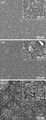
도 1은 실험예들에 따라 제조된 다이아몬드 필름을 나타내는 주사 전자 현미경(Scanning Electron Microscope; SEM) 이미지이다.
도 2는 또 다른 실험예들에 따라 제조된 다이아몬드 필름을 나타내는 SEM 이미지이다.
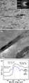
도 3은 실험예들에 따라 제조된 다이아몬드 필름의 x-선 흡수 미세 구조(Near Edge X-ray Absorption Fine Structure; NEXAFS) 스펙트럼을 나타내는 그래프이다.
도 4는 실험예들에 따라 제조된 다이아몬드 필름의 x-선 회절(x-ray diffraction; XRD) 패턴을 나타내는 그래프이다.
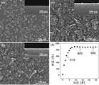
도 5는 일 실험예에 따라 제조된 다상(polyphase) 탄소 나노구조물의 고분해능 주사 전자 현미경(High Resolution Scanning Electron Microscope; HR-SEM) 이미지이다.
도 6은 일 실험예에 따라 제조된 다상 탄소 나노구조물의 또 다른 HR-SEM 이미지이다.
도 7은 일 실험예에 따라 제조된 다상 탄소 나노구조물의 고분해능 투과 전자 현미경(High Resolution Transmission Electron Microscope; HR-TEM) 이미지이다.
도 8은 일 실험예에 따라 제조된 다상 탄소 나노구조물의 또 다른 HR-TEM 이미지, 선택 영역 전자 회절(selected area electron diffraction) 패턴 및 전자에너지손실분광(electron energy loss spectroscopy) 스펙트럼을 나타낸다.
도 9는 일 실험예에 따라 제조된 다상 탄소 나노구조물의 HR-SEM 이미지 및 시간 대비 성장 온도 그래프를 나타낸다.
도 10은 일 실험예에 따라 제조된 다상 탄소 나노구조물의 또 다른 HR-TEM 이미지이다.1 is a Scanning Electron Microscope (SEM) image showing a diamond film prepared according to Experimental Examples.
Figure 2 is an SEM image showing a diamond film prepared according to another experimental example.
FIG. 3 is a graph showing Near Edge X-ray Absorption Fine Structure (NEXAFS) spectra of diamond films prepared according to Experimental Examples.
Figure 4 is a graph showing the x-ray diffraction (XRD) pattern of the diamond film prepared according to the experimental examples.
FIG. 5 is a High Resolution Scanning Electron Microscope (HR-SEM) image of a polyphase carbon nanostructure prepared according to one experimental example. FIG.
6 is another HR-SEM image of a multiphase carbon nanostructure prepared according to one experimental example.
7 is a High Resolution Transmission Electron Microscope (HR-TEM) image of a multiphase carbon nanostructure prepared according to one experimental example.
FIG. 8 shows another HR-TEM image, selected area electron diffraction pattern, and electron energy loss spectroscopy spectrum of a multiphase carbon nanostructure prepared according to one experimental example.
Figure 9 shows the HR-SEM image of the multi-phase carbon nanostructures prepared according to one experimental example and a graph of growth temperature versus time.
10 is another HR-TEM image of a multiphase carbon nanostructure prepared according to one experimental example.
이하에서는, 도면을 참조하여 본 발명의 몇몇 실시예들을 구체적으로 설명한다. 그러나, 본 발명이 하기 실시예들에 의하여 제한되는 것은 아니다.Hereinafter, some embodiments of the present invention will be described in detail with reference to the drawings. However, the present invention is not limited by the following examples.
실시예들은 다상(polyphase) 탄소 나노구조물 및 이의 제조 방법에 대한 것이다. 다상 탄소 나노구조물은 그래핀(graphene) 외장 및 이에 삽입된 다이아몬드 나노플레이크(diamond nanoflake; DNF)를 포함할 수 있다.Examples relate to polyphase carbon nanostructures and methods for their preparation. Multiphase carbon nanostructures may include graphene sheaths and diamond nanoflakes (DNF) embedded therein.
본 명세서에서, DNF는 다이아몬드로 이루어지며 나노 미터 수준의 크기를 갖는 임의의 판상형 다이아몬드 구조체를 지칭하도록 의도되며, 다이아몬드 나노판(diamond nanoplatelet) 또는 다른 상이한 명칭으로 지칭될 수도 있다. 또한, 본 명세서에서 판상형이란 전체적으로 2차원 형상의 표면을 갖는 것을 의미하도록 의도되며, 반드시 표면의 전체 부분이 완전한 평탄면인 것을 의미하지 않는다. 따라서, 본 발명의 실시예들에서 DNF는, 다이아몬드 나노로드(diamond nanorod) 또는 다이아몬드 나노와이어(diamond nanowire)와 구별될 수 있을 정도로 길이 방향에 수직한 방향에서 상대적으로 넓은 면적을 갖는 판형 구조체를 지칭하도록 의도되며, 특정 크기 또는 형상 등에 한정되지 않는다.In this specification, DNF is intended to refer to any plate-shaped diamond structure made of diamond and having a size on the order of nanometers, and may also be referred to as diamond nanoplatelet or other different names. Further, in this specification, the plate shape is intended to mean having a surface of a two-dimensional shape as a whole, and does not necessarily mean that the entire portion of the surface is a completely flat surface. Thus, in embodiments of the present invention, DNF refers to a plate-like structure having a relatively large area in a direction perpendicular to the length direction to be distinguishable from diamond nanorods or diamond nanowires. It is intended to be not limited to a particular size or shape, and the like.
그래핀 외장은 하나 이상의 개별 그래핀 층으로 이루어질 수 있다. 일 실시예에서, 그래핀 외장은 다중층 그래핀(few-layer graphene; FLG)으로 이루어진다. 또한 일 실시예에서, 그래핀 외장의 개별 그래핀 층 각각은 다이아몬드 나노플레이크의 (111) 면과 평행하게 배열된다. 이는 상세히 후술한다.The graphene sheath may consist of one or more individual graphene layers. In one embodiment, the graphene sheath is made of multiple layer graphene (FLG). Also in one embodiment, each of the individual graphene layers of the graphene sheath are arranged parallel to the (111) face of the diamond nanoflakes. This will be described later in detail.
몇몇 실시예들에서, 다상 탄소 나노구조물은 그래핀 외장 및 DNF를 에워싸는 다이아몬드 필름을 포함하는 복합막의 형태일 수 있다. 이때 다이아몬드 필름은 무도핑(undoped) 나노 결정질 다이아몬드(nano-crystalline diamond; NCD) 필름일 수도 있다. 또한, 본 명세서에서 NCD는 나노미터 수준의 결정 크기를 갖는 임의의 다이아몬드 구조를 지칭하며, 별도로 구분하여 명시되지 않을 경우 초나노 결정질 다이아몬드(Ultrananocrystalline diamond; UNCD)를 포함할 수도 있는 것으로 의도된다.In some embodiments, the multiphase carbon nanostructures may be in the form of a composite film comprising a graphene sheath and a diamond film surrounding the DNF. In this case, the diamond film may be an undoped nano-crystalline diamond (NCD) film. In addition, NCD herein refers to any diamond structure having a nanometer-level crystal size, and is intended to include ultrananocrystalline diamond (UNCD) unless otherwise specified.
실시예들에 따른 다상 탄소 나노구조물은 기체상 합성(gas phase synthesis) 방법에 의하여 제조될 수 있다. 일 실시예에서, 다상 탄소 나노구조물은 열 필라멘트 화학기상증착(Hot Filament Chemical Vapor Deposition; HF-CVD) 공정에 의하여 제조된다. HF-CVD에서는 탄화수소(CH4) 및 수소(H2)를 포함하는 원료 기체를 사용하여 기판상에 탄소 물질을 증착하되, 다상 탄소 나노구조물이 형성되도록 기판의 온도 및/또는 원료 기체에서 탄화수소(CH4)의 비율을 제어할 수 있다. 일 실시예에서, 원료 기체에서 탄화수소(CH4)의 비율은 1 % 이하로 조절된다. 이하에서는, 다상 탄소 나노구조물을 제조하기 위한 HF-CVD의 공정 파라미터를 도출하기 위하여, 본 발명의 발명자들에 의하여 수행된 몇몇 실험예에 대하여 상세히 설명한다. 그러나, 이하의 실험예들에 의하여 본 발명의 범위가 한정되는 것은 아니다.Polyphase carbon nanostructures according to embodiments may be prepared by a gas phase synthesis method. In one embodiment, the multiphase carbon nanostructures are prepared by a Hot Filament Chemical Vapor Deposition (HF-CVD) process. In HF-CVD, a carbonaceous material is deposited on a substrate using a precursor gas containing hydrocarbons (CH4 ) and hydrogen (H2 ), but the hydrocarbons at the substrate temperature and / or in the precursor gas are formed such that the polyphase carbon nanostructures are formed. CH4 ) can be controlled. In one embodiment, the proportion of hydrocarbon (CH4 ) in the feed gas is adjusted to 1% or less. Hereinafter, some experimental examples performed by the inventors of the present invention will be described in detail in order to derive process parameters of HF-CVD for producing multiphase carbon nanostructures. However, the scope of the present invention is not limited by the following experimental examples.
다상 탄소 나노구조물은 실리콘(Si)으로 이루어진 기판상에 형성될 수 있다. 예를 들어, 지름 약 4 인치(inch), 두께 약 0.5 mm, 표면 방향 (100)을 가지며, p-형 보론(boron) 도핑되고, 약 1 내지 10 Ω·cm의 저항을 갖는 Si 웨이퍼(wafer)가 사용될 수 있다. 그러나, 이는 예시적인 것으로서 실시예들에서 사용 가능한 기판의 종류는 이에 한정되는 것은 아니다. 나노 다이아몬드 입자를 포함하는 메탄올(methanol) 현탁액으로부터 초음파를 이용하여 기판상에 나노 다이아몬드 파우더(powder) 시드(seed)가 형성될 수도 있다. HF-CVD 공정을 위한 기판 처리 및 시드 물질 형성 공정에 대해서는 본 발명의 기술분야에서 잘 알려져 있으므로, 본 발명의 요지를 명확하게 하기 위하여 본 명세서에서는 상세한 설명을 생략한다.Polyphase carbon nanostructures may be formed on a substrate made of silicon (Si). For example, Si wafers having a diameter of about 4 inches, a thickness of about 0.5 mm, a surface orientation of 100, p-type boron doping and a resistivity of about 1 to 10? ) Can be used. However, this is an exemplary one, and the types of substrates usable in the embodiments are not limited thereto. Nanodiamond powder seeds may be formed on a substrate using ultrasonic waves from a methanol suspension containing nanodiamond particles. Since the substrate processing and the seed material forming process for the HF-CVD process are well known in the technical field of the present invention, a detailed description thereof will be omitted in order to clarify the gist of the present invention.
본 명세서에 기재된 실험예들에 따른 HF-CVD 공정에 있어, 챔버 내의 압력은 약 7.5 Torr로 유지되었으며, 원료 기체는 약 100 sccm의 유속으로 반응 챔버 내에 주입되었다. 필라멘트 온도(TF)는 약 2400 ℃로 유지되었다. 원료 기체는 수소(H2) 기체 내에 탄화수소(CH4)가 혼합된 기체로 이루어지되, 탄화수소(CH4)의 비율은 약 0.5 % 내지 약 5 %의 범위에서 조절되었다. 성장 온도(TG), 즉, 다이아몬드 필름이 증착될 기판의 온도는 약 830 ℃ 내지 약 950 ℃의 범위에서 조절되었다.In the HF-CVD process according to the experimental examples described herein, the pressure in the chamber was maintained at about 7.5 Torr and the feed gas was injected into the reaction chamber at a flow rate of about 100 sccm. The filament temperature TF was maintained at about 2400 ° C. The feed gas is composed of a gas mixed with hydrocarbons (CH4 ) in hydrogen (H2 ) gas, and the ratio of hydrocarbons (CH4 ) is adjusted in the range of about 0.5% to about 5%. The growth temperature TG , that is, the temperature of the substrate on which the diamond film is to be deposited, was adjusted in the range of about 830 ° C. to about 950 ° C.
합성된 다이아몬드 필름의 구조 및 결정립 크기는 고분해능 주사 전자 현미경(High Resolution Scanning Electron Microscope; HR-SEM), 고분해능 투과 전자 현미경(High Resolution Transmission Electron Microscope; HR-TEM), x-선 회절(x-ray diffraction; XRD) 장비, 근접 에지 x-선 흡수 미세 구조(Near Edge X-ray Absorption Fine Structure; NEXAFS) 장비 등의 장치를 이용하여 측정되었다. 또한, 다이아몬드 필름의 전기 전도도를 측정하기 위하여 반 데르 포(van der Pauw) 방법을 채용한 홀 측정(Hall measurement) 기법이 이용되었다.The structure and grain size of the synthesized diamond film were characterized by High Resolution Scanning Electron Microscope (HR-SEM), High Resolution Transmission Electron Microscope (HR-TEM), and X-ray Diffraction (x-ray). Diffraction (XRD) equipment, Near Edge X-ray Absorption Fine Structure (NEXAFS) equipment, and the like. Also, a Hall measurement technique employing the van der Pauw method was used to measure the electrical conductivity of the diamond film.
HF-CVD 공정을 수행하기 위하여, 반응 챔버 내로 원료 기체를 주입할 수 있다. 반응 챔버 내에는 기판 및 하나 이상의 필라멘트가 구비될 수 있다. 예컨대, 필라멘트는 약 0.3 mm의 직경을 갖는 선형 필라멘트일 수도 있으나, 이에 한정되는 것은 아니다. 원료 기체 주입 후 필라멘트에 열 또는 전력을 가함으로써, 가열된 필라멘트로부터 방출되는 열전자에 의해 원료 기체를 활성화시킬 수 있다. 활성화된 원료 기체에 의하여 기판상에 탄소 물질이 증착된다. 이때, 증착되는 탄소 물질의 구조는 HF-CVD의 공정 파라미터에 적어도 부분적으로 기초하여 결정된다.In order to perform the HF-CVD process, raw gas may be injected into the reaction chamber. The reaction chamber may be provided with a substrate and one or more filaments. For example, the filament may be a linear filament having a diameter of about 0.3 mm, but is not limited thereto. By applying heat or electric power to the filament after the raw material gas injection, the raw material gas can be activated by hot electrons emitted from the heated filament. Carbon material is deposited on the substrate by the activated raw gas. The structure of the deposited carbon material is then determined based at least in part on the process parameters of the HF-CVD.
하기 표 1은, 본 발명의 발명자들에 의한 실험에서 HF-CVD 공정에 사용된 파라미터 및 이러한 파라미터를 적용한 HF-CVD 공정에 의하여 생성된 다이아몬드 필름의 특성을 나타낸다.Table 1 below shows the parameters used in the HF-CVD process in the experiment by the inventors of the present invention and the properties of the diamond film produced by the HF-CVD process to which such parameters were applied.
번호Sample
number
크기(nm)Crystal grain
Size (nm)
표 1에서 샘플 번호 H-1 내지 H-3(이하, H 시리즈라고 한다)은 HF-CVD 공정에 있어 원료 기체 내의 탄화수소(CH4) 농도가 약 5 %인 상태에서 기판 온도(TG)를 각각 약 830, 약 890 및 약 950 ℃로 변화시키면서 형성된 다이아몬드 필름의 구조, 결정립 크기 및 전도도를 나타낸다.In Table 1, sample numbers H-1 to H-3 (hereinafter referred to as H series) indicate the substrate temperature (TG ) in the HF-CVD process with a hydrocarbon (CH4 ) concentration of about 5%. The structure, grain size and conductivity of the diamond film formed while varying from about 830, about 890 and about 950 ° C., respectively.
또한, 표 1에서 샘플 번호 L-1 내지 L-3(이하, L 시리즈라고 한다)은 원료 기체 내의 탄화수소(CH4) 농도가 약 0.5 %인 상태에서 기판 온도(TG)를 각각 약 830, 약 890 및 약 950 ℃로 변화시키면서 형성된 다이아몬드 필름의 구조, 결정립 크기 및 전도도를 나타낸다.In addition, in Table 1, the sample numbers L-1 to L-3 (hereinafter referred to as L series) are each used at a substrate temperature TG of about 830, with a hydrocarbon (CH4 ) concentration of about 0.5% in the source gas. The structure, grain size, and conductivity of the diamond film formed while varying between about 890 and about 950 ° C. are shown.
즉, H 시리즈는 원료 기체 중의 탄화수소(CH4) 농도가 상대적으로 높은 HF-CVD 공정의 결과를 나타내며, L 시리즈는 원료 기체 중의 탄화수소(CH4) 농도가 상대적으로 낮은 HF-CVD 공정의 결과를 나타낸다.That is, the H series shows the result of the HF-CVD process with a relatively high concentration of hydrocarbon (CH4 ) in the feed gas, and the L series shows the result of the HF-CVD process with a relatively low concentration of hydrocarbon (CH4 ) in the feed gas. Indicates.
도 1 및 도 2는 표 1에 도시된 HF-CVD 공정 파라미터를 적용한 실험예들에 따라 제조된 다이아몬드 필름을 나타내는 SEM 이미지이다. 도 1의 (a) 내지 (c)는 각각 표 1의 샘플 번호 H-1 내지 H-3에 대응되며, 도 2의 (a) 내지 (c)는 각각 표 1의 샘플 번호 L-1 내지 L-3에 대응된다.1 and 2 are SEM images showing a diamond film prepared according to the experimental examples applying the HF-CVD process parameters shown in Table 1. (A) to (c) of FIG. 1 respectively correspond to sample numbers H-1 to H-3 of Table 1, and (a) to (c) of FIG. 2 respectively show sample numbers L-1 to L of Table 1, respectively. Corresponds to -3.
또한, 도 3은 표 1에 도시된 실험예들에 따라 제조된 다이아몬드 필름의 NEXAFS 스펙트럼을 나타내는 그래프이다. 도 3의 (a) 내지 (c)는 각각 표 1의 샘플 번호 H-1 내지 H-3에 대응되며, 도 3의 (d) 내지 (f)는 각각 표 1의 샘플 번호 L-1 내지 L-3에 대응된다. 또한, 도 3의 (g)는 실험예들에 의해 생성된 다이아몬드 필름과의 비교를 위해 고배향성 열분해 흑연(Highly Ordered Pyrolytic Graphite; HOPG)의 NEXAFS 스펙트럼을 나타낸다.In addition, Figure 3 is a graph showing the NEXAFS spectrum of the diamond film prepared according to the experimental examples shown in Table 1. (A) to (c) of FIG. 3 correspond to sample numbers H-1 to H-3 of Table 1, respectively, and (d) to (f) of FIG. 3 respectively represent sample numbers L-1 to L of Table 1, respectively. Corresponds to -3. In addition, Figure 3 (g) shows the NEXAFS spectrum of Highly Ordered Pyrolytic Graphite (HOPG) for comparison with the diamond film produced by the experimental examples.
또한, 도 4는 표 1에 도시된 실험예들 중 L 시리즈에 따라 제조된 다이아몬드 필름의 XRD 패턴을 나타내는 그래프이다. 도 4의 (a) 내지 (c)는 각각 표 1의 샘플 번호 L-1 내지 L-3에 대응된다.In addition, Figure 4 is a graph showing the XRD pattern of the diamond film prepared according to the L series of the experimental examples shown in Table 1. 4 (a) to 4 (c) correspond to sample numbers L-1 to L-3 in Table 1, respectively.
표 1을 참조하면, L 시리즈 중 샘플 번호 L-2에서 DNF / FLG / UNCD로 이루어지는 복합막, 즉, 다상 탄소 나노구조물이 형성되었다. 도 2의 (b)에 도시되는 바와 같이, 상기 다상 탄소 나노구조물은 로드(rod)와 유사한 형상을 가지나, 도 2의 (b)의 우측 상단과 같이 더욱 확대할 경우 UNCD 모체에 삽입되어 있는 플레이크(flake)형 구조물의 노출 부분인 것으로 확인할 수 있다. 삽입된 플레이크형 구조물은 DNF 및 FLG로 이루어지며, 이에 대해서는 상세히 후술한다. 이와 같은 다상 탄소 나노구조물은 전체 필름의 표면 부근에서는 크기가 감소하나 여전히 관찰 가능하다.Referring to Table 1, a composite membrane made of DNF / FLG / UNCD, that is, a polyphase carbon nanostructure was formed in Sample No. L-2 in the L series. As shown in (b) of FIG. 2, the polyphase carbon nanostructure has a rod-like shape, but when the lens is further enlarged as shown in the upper right corner of FIG. It can be seen that the exposed portion of the (flake) -type structure. The inserted flake structure consists of DNF and FLG, which will be described later in detail. Such polyphase carbon nanostructures decrease in size near the surface of the entire film but are still observable.
도 3의 (d) 내지 (f)를 참조하면, 샘플 번호 L-1 내지 L-3의 NEXAFS 스펙트럼은 모두 광자 에너지가 약 289.3 eV일 때 피크(peak)를 가지며 약 302.2 eV일 때 딥(dip)을 갖는 유사한 경향성을 나타낸다. 이는 다상 탄소 나노구조물의 주된 위상이 탄소의 다른 형태가 아닌 다이아몬드임을 나타낸다. 이 점은, 도 4에 도시된 것과 같이, 입사각이 약 43.9도[(111) 면], 약 75.3도[(220) 면] 및 약 91.5도[(311) 면]일 때 피크가 나타내는 XRD 회절 특성으로부터도 확인할 수 있다. 또한, 이상에 기재한 다이아몬드의 (111), (220) 및 (311) 면은 HR-TEM 이미지로부터도 확인할 수 있으며, 이는 도 8을 참조하여 상세히 후술한다.Referring to FIGS. 3D through 3F, the NEXAFS spectra of the sample numbers L-1 to L-3 all have a peak when the photon energy is about 289.3 eV and a dip when about 302.2 eV. Similar trend with). This indicates that the predominant phase of polyphase carbon nanostructures is diamond, not other forms of carbon. This is the XRD diffraction exhibited by the peak when the incident angle is about 43.9 degrees [(111) plane], about 75.3 degrees [(220) plane] and about 91.5 degrees [(311) plane], as shown in FIG. It can also be confirmed from a characteristic. In addition, the (111), (220) and (311) planes of the diamond described above can also be confirmed from an HR-TEM image, which will be described later in detail with reference to FIG. 8.
도 5는 샘플 번호 L-2의 다상 탄소 구조물의 단면을 배율을 달리하여 나타내는 HR-SEM 이미지들이다. 도시되는 바와 같이, UNCD에 삽입된 다이아몬드 구조체가, 점선 화살표로 지시된 넓고 평탄한 단면과 실선 화살표로 지시된 좁고 긴 단면을 갖는 것을 확인할 수 있다. 이는 다상 탄소 구조물이 로드 또는 와이어가 아닌 플레이크 형상이며, 플레이크가 성장 프론트(front)에 대해 수직 또는 이에 근접한 각도로 정렬되고, 플레이크 표면이 무작위한 결정면을 갖는 것을 의미한다.5 are HR-SEM images showing cross-sectional views of the polyphase carbon structure of Sample No. L-2 with different magnifications. As shown, it can be seen that the diamond structure inserted in the UNCD has a wide and flat cross section indicated by a dashed arrow and a narrow long cross section indicated by a solid arrow. This means that the polyphase carbon structure is flake-shaped, not rod or wire, the flakes are aligned at an angle perpendicular to or close to the growth front, and the flake surface has a random crystal plane.
도 6은 표 1에 도시된 샘플 번호 L-2의 다상 탄소 구조물의 단면을 나타내는 또 다른 HR-SEM 이미지이다. 도 6의 (a)는 성장면 부근의 절단면의 단면을 나타내며, 도 6의 (b)는 성장면을 나타낸다. 도 6의 (a) 및 (b)에서 다상 탄소 구조물에 해당하는 부분은 화살표로 지시되었다. 도시되는 바와 같이, 플레이크 형상의 다상 탄소 구조물이 성장면에서 노출되는 것을 확인할 수 있다.FIG. 6 is another HR-SEM image showing a cross section of the multiphase carbon structure of Sample No. L-2 shown in Table 1. FIG. Fig. 6A shows a cross section of the cut surface near the growth surface, and Fig. 6B shows the growth surface. In FIGS. 6A and 6B, portions corresponding to the multiphase carbon structures are indicated by arrows. As shown, it can be seen that the flake-shaped polyphase carbon structure is exposed on the growth surface.
도 7은 표 1에 도시된 샘플 번호 L-2의 다상 탄소 구조물의 단면을 나타내는 또 다른 HR-TEM 이미지이다. 도 7의 (a)를 참조하면, 단면에서 점선 화살표로 지시된 넓은 평탄한 단면과 실선 화살표로 지시된 좁고 긴 단면이 함께 존재하므로, 다상 탄소 구조물이 판상형인 것을 다시 한 번 확인할 수 있다.FIG. 7 is another HR-TEM image showing a cross section of the multiphase carbon structure of Sample No. L-2 shown in Table 1. FIG. Referring to FIG. 7A, since a wide flat cross section indicated by a dotted arrow and a narrow long cross section indicated by a solid arrow exist together in the cross section, it may be confirmed that the multiphase carbon structure is plate-shaped.
도 7의 (a)는 절단면 투과 전자 현미경(Cross Sectional TEM)으로 관찰된 다상 탄소 구조물의 단면사진이다. 사진 왼편의 검은 층은 실리콘 기판이며, 그와 인접한, 우측 대부분을 점유한 부분이 다이아몬드 박막 층이다. 박막은 기판으로부터 기판에 수직한 방향으로 성장했다. 이 다이아몬드 박막 층의 단면에서 희게 보이는 부위가 UNCD 기지상(matrix)인데, 그 보다 검게 보이는 얇고 긴 막대형태의 미세 구조체(실선 화살표로 지시됨)와, 넓은 평탄한 면 형태의 미세 구조체(점선 화살표로 지시됨)가 함께 존재한다. 이 두 가지 구조체의 성장방향은 기판과 거의 수직한 방향 혹은 이에 근접한 방향으로 정렬된 특징을 보인다.FIG. 7A is a cross-sectional photograph of a multiphase carbon structure observed with a cross section TEM. FIG. The black layer on the left side of the picture is a silicon substrate, and the portion occupying most of the right side adjacent thereto is a diamond thin film layer. The thin film grew from the substrate in a direction perpendicular to the substrate. In the cross section of this diamond thin film layer, the white-looking part is the UNCD matrix, which is thinner and longer-shaped microstructures (indicated by solid arrows), and wider planar microstructures (indicated by dashed arrows). Together). The growth direction of these two structures is characterized by being aligned in a direction substantially perpendicular to or close to the substrate.
도5및 도6의 관찰결과를 고려하면, 점선 화살표로 지시한 부분은 다상 탄소 구조물에서 플레이크의 넓은 면 방향이, 실선으로 지시한 얇은 막대부분은 플레이크의 단면이 TEM 관찰면에 드러난 형태로 판단된다. 즉, 평탄한 단면과 좁고 긴 단면의 형태는 실제로 동일한 다상 탄소 구조물에 의한 것으로, 도5 및 도 6의 결과를 뒷받침한다. 평탄한 형태의 단면에 비해 좁고 긴 단면이 주로 관찰되는 이유는 TEM 관찰을 위해 제작되는 포일(foil)의 면 방향과, 평탄한 형태의 단면의 방향이 일치할 확률이 매우 낮기 때문이다.Considering the observation results of FIGS. 5 and 6, the portion indicated by the dotted arrow indicates that the wide surface direction of the flakes in the polyphase carbon structure is thin, and the thin rod portion indicated by the solid line indicates that the cross section of the flake is revealed on the TEM observation surface. do. That is, the shape of the flat cross section and the narrow and long cross section are actually due to the same multiphase carbon structure, which supports the results of FIGS. 5 and 6. The reason why narrow and long cross sections are mainly observed compared to the flat cross section is that the plane direction of the foil manufactured for TEM observation and the flat cross section have a very low probability of matching.
이와 달리, 도 5와 도 6의 (a)의 SEM 이미지들에서 평탄한 형태의 단면이 빈번히 관찰되는 이유는, 다상 탄소 구조물을 절단할 때 DNF와 UNCD 기지상 사이에 존재하는 그래핀 층 상호 간의 결합 강도가 매우 약하기 때문에, 그로부터 파괴 경로(fracture path)가 발생하면서 평탄한 형태의 단면이 발생하는 것이다.On the contrary, the reason why the cross section of the flat shape is frequently observed in the SEM images of FIGS. 5 and 6 (a) is that the bonding strength between the graphene layers present between the DNF and UNCD matrix phases when cutting the multiphase carbon structure. Is very weak, and a fracture path is generated therefrom, resulting in a flat cross section.
도 7의 (b) 및 (c)는 도 7의 (a)에 도시된 다상 탄소 구조물에서 점선 화살표로 지시된 넓고 평탄한 단면 부분을 보다 고배율로 관찰한 HR-TEM 이미지이다. 도 7의 (b) 및 (c)는 각각 기판과 인접한 한쪽 끝 및 이의 반대편 끝을 나타낸다. 도시되는 바와 같이, 다상 탄소 구조물은 (111) 쌍정판(twin plate)을 가지며, 쌍정판의 경계(Twin boundary)는 다이아몬드 필름 전체의 성장 방향(즉, 기판 표면에 수직한 방향)과 대략적으로 정렬된다.(B) and (c) of FIG. 7 are HR-TEM images of the multi-phase carbon structure shown in FIG. 7 (b) and 7 (c) show one end adjacent to the substrate and the other end thereof, respectively. As shown, the multiphase carbon structure has a (111) twin plate, with the twin boundary roughly aligned with the growth direction of the diamond film as a whole (i.e., perpendicular to the substrate surface). do.
도 8의 (a) 및 (b)는 도 7의 (a)에 도시된 다상 탄소 구조물에서 실선 화살표로 지시된 좁고 긴 단면 부분을 확대하여 나타낸 HR-TEM 이미지이다. 또한, 도 8의 (a)의 삽입 그림(inset)은 다상 탄소 구조물의 선택 영역 전자 회절(Selected Area Electron Diffraction; SAED) 패턴을 나타낸다. 또한, 도 8의 (c)는 다상 탄소 구조물의 전자에너지손실분광(Electron Energy Loss Spectroscopy; EELS) 스펙트럼을 나타낸다.8A and 8B are enlarged HR-TEM images of narrow and long cross-sectional portions indicated by solid arrows in the multiphase carbon structure shown in FIG. In addition, an inset of FIG. 8A illustrates a selected area electron diffraction (SAED) pattern of the multiphase carbon structure. In addition, Figure 8 (c) shows the Electron Energy Loss Spectroscopy (EELS) spectrum of the multiphase carbon structure.
도 8의 (a)를 참조하면 다상 탄소 구조물은 약 5 내지 10 nm의 폭을 가지며 약 300 nm의 길이를 갖는다. 도 8의 (b)에 도시된 것과 같이 이를 더 확대하면, 다상 탄소 구조물은 그래핀 외장 층들 사이에 DNF가 삽입된 샌드위치(sandwich) 구조를 갖는다. 약 2.06 Å의 간격으로 배열된 DNF의 (111) 면들이 전체 다이아몬드 필름의 길이 방향을 따라 연장된다. 또한, 약 1 내지 2 nm 두께의 그래핀 외장이 DNF의 바깥쪽에 위치한다. 그래핀 외장은 약 3.4 Å의 간격으로 개별 그래핀 층들이 중첩된 FLG로 이루어진다.Referring to FIG. 8A, the multiphase carbon structure has a width of about 5 to 10 nm and a length of about 300 nm. Further enlarged as shown in FIG. 8B, the multiphase carbon structure has a sandwich structure in which DNF is inserted between graphene facing layers. The (111) faces of DNF, arranged at intervals of about 2.06 mm 3, extend along the length of the entire diamond film. Also, about 1-2 nm thick graphene sheath is located outside of DNF. The graphene sheath consists of FLG with individual graphene layers superimposed at intervals of about 3.4 mm 3.
다상 탄소 구조물의 코어 및 외장이 각각 다이아몬드 및 그래핀으로 이루어지는 것이라는 점은, 도 8의 (c)에 도시된 EELS 스펙트럼에서 코어 영역의 그래프(810)가 약 289.3 eV에서 피크를 가지며 약 302.2 eV에서 딥을 갖는 것과, 외장 영역의 그래프(820)가 약 285.5 eV에서 피크를 갖는 것으로부터도 확인할 수 있다.The core and sheath of the polyphase carbon structure consists of diamond and graphene, respectively, indicating that the
도 9는 표 1에 도시된 샘플 번호 L-2의 다상 탄소 구조물의 HR-SEM 이미지 및 시간 대비 성장 온도 그래프를 나타낸다. 도 9의 (a) 내지 (c)는 각각 전체 다이아몬드 필름의 성장 과정에서 램프(ramp) 단계, 램프 단계로부터 10분 경과 후, 및 램프 단계로부터 20분 경과 후의 평면도 및 단면도(삽입 그림)를 나타낸다. 또한, 도 9의 (d)에서 화살표로 지시된 세 개의 점(910, 920, 930)은 각각 램프 단계, 램프 단계로부터 10분 경과 후, 및 램프 단계로부터 20분 경과 후의 성장 온도의 변화를 나타낸다.9 shows an HR-SEM image and a graph of growth temperature over time of the multiphase carbon structure of Sample No. L-2 shown in Table 1. FIG. 9 (a) to 9 (c) show a plan view and a cross-sectional view (insertion diagram) after the ramp stage, 10 minutes after the ramp stage, and 20 minutes after the ramp stage, respectively, in the growth process of the entire diamond film. . In addition, three
도시되는 바와 같이, 성장 온도는 램프 단계로부터 약 7분 경과 후 포화된다. 도 9의 (a)를 참조하면, 초기 램프 단계에서는 다상 탄소 구조물이 형성되지 않는다. 도 9의 (b)를 참조하면 램프 단계로부터 약 10분 경과 후 UNCD 모체 내에 I자 모양의 다이아몬드 구조체가 형성되며, 이는 도 9의 (c)에 도시된 것과 같이 램프 단계로부터 약 20분 경과 후에도 유지된다. 이는 DNF 구조의 핵 형성(nucleation)이 성장 초기에 나타나는 흑연 단계와 밀접하게 관련이 있음을 의미한다.As shown, the growth temperature is saturated after about 7 minutes from the ramp stage. Referring to FIG. 9A, no polyphase carbon structure is formed in the initial ramp stage. Referring to (b) of FIG. 9, an I-shaped diamond structure is formed in the UNCD matrix after about 10 minutes from the ramp stage, and even after about 20 minutes from the ramp stage, as shown in FIG. maintain. This means that nucleation of the DNF structure is closely related to the graphite phase that occurs early in growth.
도 10의 (a)는 도 9의 (c)에 도시된 다상 탄소 구조물의 평면도를 배율을 달리하여 나타낸 HR-TEM 이미지이며, 도 10의 (b)는 도 10의 (a)의 점선 부분의 확대도이다. 도 10의 (a)에 도시되는 바와 같이, 저배율에서도 DNF의 판상형 구조가 명확하게 나타낸다. 또한, 도 10의 (b)에 도시되는 것과 같이, DNF는 복수 개의 쌍정판을 포함한다. 도 10에서는 FLG 층은 나타나지 않았으며, 이는 FLG가 다이아몬드 필름의 성장 초기 단계가 아닌 보다 이후의 단계에서 형성된다는 것을 의미한다.(A) of FIG. 10 is an HR-TEM image of the multi-phase carbon structure shown in (c) of FIG. 9 at different magnifications, and (b) of FIG. 10 is a dotted line of FIG. It is an enlarged view. As shown in Fig. 10A, the plate-like structure of DNF is clearly shown even at low magnification. In addition, as shown in FIG. 10B, the DNF includes a plurality of twin plates. In FIG. 10, no FLG layer is shown, which means that the FLG is formed at a later stage rather than at the early stage of growth of the diamond film.
이상의 실험예들에 기초하여, HF-CVD 공정에서 원료 기체 중의 탄화수소(CH4) 비율 및/또는 기판의 온도를 제어함으로써 UNCD에 다이아몬드 구조체가 삽입된 다상 탄소 나노구조물을 형성할 수 있다. 또한, 이때 삽입된 다이아몬드 구조체는 FLG 외장 내에 DNF가 삽입된 구조를 갖는다. 표 1에 기재된 것과 같이, DNF / FLG / UNCD의 복합 구조를 갖는 다상 탄소 나노구조물은, NDF 및 FLG의 존재로 인하여, 흑연을 포함하지 않는 종래의 NCD 또는 UNCD 필름과 비교하여 약 10,000배 내지 100,000배 큰 전기 전도도를 갖는 이점이 있다.Based on the above experimental examples, it is possible to form a multiphase carbon nanostructure in which a diamond structure is inserted in UNCD by controlling the hydrocarbon (CH4 ) ratio in the raw material gas and / or the temperature of the substrate in the HF-CVD process. In addition, the inserted diamond structure has a structure in which the DNF is inserted into the FLG sheath. As shown in Table 1, multiphase carbon nanostructures having a composite structure of DNF / FLG / UNCD, due to the presence of NDF and FLG, are about 10,000 to 100,000 compared to conventional NCD or UNCD films that do not contain graphite. There is an advantage of having twice the electrical conductivity.
이상에서 살펴본 본 발명은 도면에 도시된 실시예들을 참고로 하여 설명하였으나 이는 예시적인 것에 불과하며 당해 분야에서 통상의 지식을 가진 자라면 이로부터 다양한 변형 및 실시예의 변형이 가능하다는 점을 이해할 것이다. 그러나, 이와 같은 변형은 본 발명의 기술적 보호범위 내에 있다고 보아야 한다. 따라서, 본 발명의 진정한 기술적 보호범위는 첨부된 특허청구범위의 기술적 사상에 의해서 정해져야 할 것이다.While the invention has been shown and described with reference to certain embodiments thereof, it will be understood by those skilled in the art that various changes and modifications may be made therein without departing from the spirit and scope of the invention as defined by the appended claims. However, it should be understood that such modifications are within the technical scope of the present invention. Therefore, the true technical protection scope of the present invention will be defined by the technical spirit of the appended claims.
Claims (10)
Translated fromKorean상기 그래핀 외장에 삽입된 다이아몬드 나노플레이크를 포함하는 것을 특징으로 하는 다상 탄소 나노구조물.
A graphene sheath consisting of at least one graphene layer; And
Multiphase carbon nanostructures comprising diamond nanoflakes inserted into the graphene sheath.
상기 그래핀 외장은 다중층 그래핀으로 이루어지는 것을 특징으로 하는 다상 탄소 나노구조물.
The method of claim 1,
The graphene sheath is a multi-phase carbon nanostructure, characterized in that consisting of multilayer graphene.
상기 하나 이상의 그래핀 층 각각은 상기 다이아몬드 나노플레이크의 (111) 면과 평행하게 배열된 것을 특징으로 하는 다상 탄소 나노구조물.
The method of claim 1,
Each of the at least one graphene layer is a multi-phase carbon nanostructure, characterized in that arranged in parallel with the (111) plane of the diamond nanoflakes.
상기 그래핀 외장을 둘러싸고 위치하는 나노 결정질 다이아몬드 필름을 더 포함하는 것을 특징으로 하는 다상 탄소 나노구조물.
The method of claim 1,
The polyphase carbon nanostructures further comprising a nanocrystalline diamond film positioned surrounding the graphene sheath.
상기 기판을 가열하는 단계;
상기 필라멘트를 가열하여 상기 원료 기체를 활성화하는 단계; 및
활성화된 상기 원료 기체로부터, 가열된 상기 기판상에 그래핀 층 및 상기 그래핀 층에 삽입된 다이아몬드 나노플레이크를 형성하는 단계를 포함하는 다상 탄소 나노구조물의 제조 방법.
Injecting a raw material gas containing hydrogen and hydrocarbon water into a reaction chamber in which the substrate and the filament are located;
Heating the substrate;
Heating the filament to activate the raw material gas; And
Forming a graphene layer and diamond nanoflakes embedded in the graphene layer on the heated substrate from the activated raw material gas.
상기 원료 기체를 주입하는 단계는, 상기 원료 기체 내의 탄화수소의 비율을 1% 이하로 조절하는 단계를 포함하는 것을 특징으로 하는 다상 탄소 나노구조물의 제조 방법.
6. The method of claim 5,
The step of injecting the raw material gas, the method of producing a multi-phase carbon nanostructures comprising the step of adjusting the proportion of hydrocarbons in the raw material gas to 1% or less.
상기 기판을 가열하는 단계는, 상기 기판을 800 ℃ 이상의 온도로 가열하는 단계를 포함하는 것을 특징으로 하는 다상 탄소 나노구조물의 제조 방법.
6. The method of claim 5,
The heating of the substrate may include heating the substrate to a temperature of 800 ° C. or higher.
상기 그래핀 층은 다중층 그래핀으로 이루어지는 것을 특징으로 하는 다상 탄소 나노구조물의 제조 방법.
6. The method of claim 5,
The graphene layer is a method for producing a multi-phase carbon nanostructure, characterized in that consisting of multilayer graphene.
상기 그래핀 층은 상기 다이아몬드 나노플레이크의 (111) 면과 평행하게 배열된 것을 특징으로 하는 다상 탄소 나노구조물의 제조 방법.
6. The method of claim 5,
The graphene layer is a method of producing a multi-phase carbon nanostructures, characterized in that arranged in parallel with the (111) plane of the diamond nanoflakes.
상기 형성하는 단계는, 상기 그래핀 층을 둘러싸고 위치하는 나노 결정질 다이아몬드 필름을 형성하는 단계를 포함하는 것을 특징으로 하는 다상 탄소 나노구조물의 제조 방법.6. The method of claim 5,
The forming step includes forming a nanocrystalline diamond film positioned surrounding the graphene layer.
Priority Applications (1)
| Application Number | Priority Date | Filing Date | Title |
|---|---|---|---|
| KR1020120137650AKR101349633B1 (en) | 2012-11-30 | 2012-11-30 | Polyphase carbon nanostructure including diamond nanoflakes embedded in graphene sheaths and method for manufacturing the same |
Applications Claiming Priority (1)
| Application Number | Priority Date | Filing Date | Title |
|---|---|---|---|
| KR1020120137650AKR101349633B1 (en) | 2012-11-30 | 2012-11-30 | Polyphase carbon nanostructure including diamond nanoflakes embedded in graphene sheaths and method for manufacturing the same |
Publications (1)
| Publication Number | Publication Date |
|---|---|
| KR101349633B1true KR101349633B1 (en) | 2014-02-25 |
Family
ID=50269346
Family Applications (1)
| Application Number | Title | Priority Date | Filing Date |
|---|---|---|---|
| KR1020120137650AExpired - Fee RelatedKR101349633B1 (en) | 2012-11-30 | 2012-11-30 | Polyphase carbon nanostructure including diamond nanoflakes embedded in graphene sheaths and method for manufacturing the same |
Country Status (1)
| Country | Link |
|---|---|
| KR (1) | KR101349633B1 (en) |
Cited By (1)
| Publication number | Priority date | Publication date | Assignee | Title |
|---|---|---|---|---|
| KR101728838B1 (en)* | 2015-01-30 | 2017-04-21 | 한국과학기술연구원 | Sensing electrode comprising interconnected diamond nanoflakes and method for manufacturing the same |
Citations (2)
| Publication number | Priority date | Publication date | Assignee | Title |
|---|---|---|---|---|
| KR20110032999A (en)* | 2009-09-24 | 2011-03-30 | 한국과학기술원 | 3D nanostructure and a method of manufacturing the nano-layer laminated on the graphene substrate |
| US20120102843A1 (en) | 2010-10-29 | 2012-05-03 | Baker Hughes Incorporated | Graphene-coated diamond particles, compositions and intermediate structures comprising same, and methods of forming graphene-coated diamond particles and polycrystalline compacts |
- 2012
- 2012-11-30KRKR1020120137650Apatent/KR101349633B1/ennot_activeExpired - Fee Related
Patent Citations (2)
| Publication number | Priority date | Publication date | Assignee | Title |
|---|---|---|---|---|
| KR20110032999A (en)* | 2009-09-24 | 2011-03-30 | 한국과학기술원 | 3D nanostructure and a method of manufacturing the nano-layer laminated on the graphene substrate |
| US20120102843A1 (en) | 2010-10-29 | 2012-05-03 | Baker Hughes Incorporated | Graphene-coated diamond particles, compositions and intermediate structures comprising same, and methods of forming graphene-coated diamond particles and polycrystalline compacts |
Non-Patent Citations (1)
| Title |
|---|
| Jae-Kap Lee, et. al., Crystalline diamond/graphite nanoflake hybrid films, 2010, Vol. 519, Pages 625-629.* |
Cited By (1)
| Publication number | Priority date | Publication date | Assignee | Title |
|---|---|---|---|---|
| KR101728838B1 (en)* | 2015-01-30 | 2017-04-21 | 한국과학기술연구원 | Sensing electrode comprising interconnected diamond nanoflakes and method for manufacturing the same |
Similar Documents
| Publication | Publication Date | Title |
|---|---|---|
| Jana et al. | Progress in CVD synthesis of layered hexagonal boron nitride with tunable properties and their applications | |
| KR101019029B1 (en) | Graphene Hybrid Materials and Methods for Making the Same | |
| Vlasov et al. | Hybrid diamond‐graphite nanowires produced by microwave plasma chemical vapor deposition | |
| KR101284059B1 (en) | Graphene-Oxide Semiconductor Heterojunction Devices, and Production Method of the Same | |
| Xu et al. | Graphene–silver nanowire hybrid films as electrodes for transparent and flexible loudspeakers | |
| US20130266729A1 (en) | Method for making strip shaped graphene layer | |
| US20140374960A1 (en) | Method for producing a graphene film | |
| US20100055464A1 (en) | Graphene and Hexagonal Boron Nitride Planes and Associated Methods | |
| Huang et al. | Substrate engineering for CVD growth of single crystal graphene | |
| KR20140093944A (en) | Rapid synthesis of graphene and formation of graphene structures | |
| US20130264193A1 (en) | Method for making strip shaped graphene layer | |
| KR20130132808A (en) | Conductive thin film containing graphene, and transparent conductive film | |
| JP5872672B2 (en) | Catalyst-free synthesis of vertically aligned CNT on SiNW array | |
| Zhuang et al. | Graphene/3C-SiC hybrid nanolaminate | |
| KR102027042B1 (en) | Array of graphene qunantum dots embedded in hexagonal boron nitride and manufacturing method for the same, electronic device comprising for the same | |
| JP2014148423A (en) | Method for producing single crystal graphene, and touch panel using single crystal graphene | |
| CN102976313A (en) | Preparation method for graphene | |
| KR101349633B1 (en) | Polyphase carbon nanostructure including diamond nanoflakes embedded in graphene sheaths and method for manufacturing the same | |
| US20130264748A1 (en) | Method for making strip shaped graphene layer | |
| US20180105426A1 (en) | Graphene and hexagonal boron nitride planes and associated methods | |
| KR101470830B1 (en) | Fabrication method of three-dimensional carbon structure and the structure thereof | |
| K Brantov | Perspective methods for producing composite materials based on carbon, silicon and silicon carbide: Progress and challenges | |
| KR101400163B1 (en) | Carbon nanotree and Synthesizing method of carbon nanotree | |
| KR20140074097A (en) | Method of preparing graphene | |
| Hong et al. | Simple, effective fabrication of layered carbon nanotube/graphene hybrid field emitters by electrophoretic deposition |
Legal Events
| Date | Code | Title | Description |
|---|---|---|---|
| A201 | Request for examination | ||
| PA0109 | Patent application | St.27 status event code:A-0-1-A10-A12-nap-PA0109 | |
| PA0201 | Request for examination | St.27 status event code:A-1-2-D10-D11-exm-PA0201 | |
| D13-X000 | Search requested | St.27 status event code:A-1-2-D10-D13-srh-X000 | |
| D14-X000 | Search report completed | St.27 status event code:A-1-2-D10-D14-srh-X000 | |
| E701 | Decision to grant or registration of patent right | ||
| PE0701 | Decision of registration | St.27 status event code:A-1-2-D10-D22-exm-PE0701 | |
| GRNT | Written decision to grant | ||
| PR0701 | Registration of establishment | St.27 status event code:A-2-4-F10-F11-exm-PR0701 | |
| PR1002 | Payment of registration fee | St.27 status event code:A-2-2-U10-U11-oth-PR1002 Fee payment year number:1 | |
| PN2301 | Change of applicant | St.27 status event code:A-5-5-R10-R13-asn-PN2301 St.27 status event code:A-5-5-R10-R11-asn-PN2301 | |
| PG1601 | Publication of registration | St.27 status event code:A-4-4-Q10-Q13-nap-PG1601 | |
| FPAY | Annual fee payment | Payment date:20161226 Year of fee payment:4 | |
| PR1001 | Payment of annual fee | St.27 status event code:A-4-4-U10-U11-oth-PR1001 Fee payment year number:4 | |
| FPAY | Annual fee payment | Payment date:20171227 Year of fee payment:5 | |
| PR1001 | Payment of annual fee | St.27 status event code:A-4-4-U10-U11-oth-PR1001 Fee payment year number:5 | |
| P22-X000 | Classification modified | St.27 status event code:A-4-4-P10-P22-nap-X000 | |
| FPAY | Annual fee payment | Payment date:20190102 Year of fee payment:6 | |
| PR1001 | Payment of annual fee | St.27 status event code:A-4-4-U10-U11-oth-PR1001 Fee payment year number:6 | |
| PC1903 | Unpaid annual fee | St.27 status event code:A-4-4-U10-U13-oth-PC1903 Not in force date:20200104 Payment event data comment text:Termination Category : DEFAULT_OF_REGISTRATION_FEE | |
| PC1903 | Unpaid annual fee | St.27 status event code:N-4-6-H10-H13-oth-PC1903 Ip right cessation event data comment text:Termination Category : DEFAULT_OF_REGISTRATION_FEE Not in force date:20200104 | |
| PN2301 | Change of applicant | St.27 status event code:A-5-5-R10-R13-asn-PN2301 St.27 status event code:A-5-5-R10-R11-asn-PN2301 |