KR101348247B1 - Liquid crystal display device - Google Patents
Liquid crystal display deviceDownload PDFInfo
- Publication number
- KR101348247B1 KR101348247B1KR1020070055623AKR20070055623AKR101348247B1KR 101348247 B1KR101348247 B1KR 101348247B1KR 1020070055623 AKR1020070055623 AKR 1020070055623AKR 20070055623 AKR20070055623 AKR 20070055623AKR 101348247 B1KR101348247 B1KR 101348247B1
- Authority
- KR
- South Korea
- Prior art keywords
- printed circuit
- circuit board
- flexible printed
- storage container
- liquid crystal
- Prior art date
- Legal status (The legal status is an assumption and is not a legal conclusion. Google has not performed a legal analysis and makes no representation as to the accuracy of the status listed.)
- Expired - Fee Related
Links
Images


Classifications
- G—PHYSICS
- G02—OPTICS
- G02F—OPTICAL DEVICES OR ARRANGEMENTS FOR THE CONTROL OF LIGHT BY MODIFICATION OF THE OPTICAL PROPERTIES OF THE MEDIA OF THE ELEMENTS INVOLVED THEREIN; NON-LINEAR OPTICS; FREQUENCY-CHANGING OF LIGHT; OPTICAL LOGIC ELEMENTS; OPTICAL ANALOGUE/DIGITAL CONVERTERS
- G02F1/00—Devices or arrangements for the control of the intensity, colour, phase, polarisation or direction of light arriving from an independent light source, e.g. switching, gating or modulating; Non-linear optics
- G02F1/01—Devices or arrangements for the control of the intensity, colour, phase, polarisation or direction of light arriving from an independent light source, e.g. switching, gating or modulating; Non-linear optics for the control of the intensity, phase, polarisation or colour
- G02F1/13—Devices or arrangements for the control of the intensity, colour, phase, polarisation or direction of light arriving from an independent light source, e.g. switching, gating or modulating; Non-linear optics for the control of the intensity, phase, polarisation or colour based on liquid crystals, e.g. single liquid crystal display cells
- G02F1/133—Constructional arrangements; Operation of liquid crystal cells; Circuit arrangements
- G02F1/1333—Constructional arrangements; Manufacturing methods
- G02F1/1345—Conductors connecting electrodes to cell terminals
- G02F1/13452—Conductors connecting driver circuitry and terminals of panels
- G—PHYSICS
- G02—OPTICS
- G02F—OPTICAL DEVICES OR ARRANGEMENTS FOR THE CONTROL OF LIGHT BY MODIFICATION OF THE OPTICAL PROPERTIES OF THE MEDIA OF THE ELEMENTS INVOLVED THEREIN; NON-LINEAR OPTICS; FREQUENCY-CHANGING OF LIGHT; OPTICAL LOGIC ELEMENTS; OPTICAL ANALOGUE/DIGITAL CONVERTERS
- G02F1/00—Devices or arrangements for the control of the intensity, colour, phase, polarisation or direction of light arriving from an independent light source, e.g. switching, gating or modulating; Non-linear optics
- G02F1/01—Devices or arrangements for the control of the intensity, colour, phase, polarisation or direction of light arriving from an independent light source, e.g. switching, gating or modulating; Non-linear optics for the control of the intensity, phase, polarisation or colour
- G02F1/13—Devices or arrangements for the control of the intensity, colour, phase, polarisation or direction of light arriving from an independent light source, e.g. switching, gating or modulating; Non-linear optics for the control of the intensity, phase, polarisation or colour based on liquid crystals, e.g. single liquid crystal display cells
- G02F1/133—Constructional arrangements; Operation of liquid crystal cells; Circuit arrangements
- G02F1/1333—Constructional arrangements; Manufacturing methods
- G02F1/133308—Support structures for LCD panels, e.g. frames or bezels
- G02F1/133314—Back frames
- G—PHYSICS
- G02—OPTICS
- G02F—OPTICAL DEVICES OR ARRANGEMENTS FOR THE CONTROL OF LIGHT BY MODIFICATION OF THE OPTICAL PROPERTIES OF THE MEDIA OF THE ELEMENTS INVOLVED THEREIN; NON-LINEAR OPTICS; FREQUENCY-CHANGING OF LIGHT; OPTICAL LOGIC ELEMENTS; OPTICAL ANALOGUE/DIGITAL CONVERTERS
- G02F1/00—Devices or arrangements for the control of the intensity, colour, phase, polarisation or direction of light arriving from an independent light source, e.g. switching, gating or modulating; Non-linear optics
- G02F1/01—Devices or arrangements for the control of the intensity, colour, phase, polarisation or direction of light arriving from an independent light source, e.g. switching, gating or modulating; Non-linear optics for the control of the intensity, phase, polarisation or colour
- G02F1/13—Devices or arrangements for the control of the intensity, colour, phase, polarisation or direction of light arriving from an independent light source, e.g. switching, gating or modulating; Non-linear optics for the control of the intensity, phase, polarisation or colour based on liquid crystals, e.g. single liquid crystal display cells
- G02F1/133—Constructional arrangements; Operation of liquid crystal cells; Circuit arrangements
- G02F1/1333—Constructional arrangements; Manufacturing methods
- G02F1/133308—Support structures for LCD panels, e.g. frames or bezels
- G02F1/133317—Intermediate frames, e.g. between backlight housing and front frame
Landscapes
- Physics & Mathematics (AREA)
- Nonlinear Science (AREA)
- Mathematical Physics (AREA)
- Chemical & Material Sciences (AREA)
- Crystallography & Structural Chemistry (AREA)
- General Physics & Mathematics (AREA)
- Optics & Photonics (AREA)
- Liquid Crystal (AREA)
Abstract
Translated fromKoreanDescription
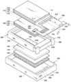
Translated fromKorean도 1은 본 발명의 제1 실시예에 따른 액정 표시 장치를 나타낸 분해 사시도이다.1 is an exploded perspective view of a liquid crystal display according to a first exemplary embodiment of the present invention.
도 2는 도 1의 A-A'선을 따라 액정 표시 장치를 자른 단면도이다.FIG. 2 is a cross-sectional view of the liquid crystal display taken along the line AA ′ of FIG. 1.
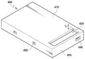
도 3은 본 발명의 제1 실시예에 따른 액정 표시 장치에 포함되는 연성 인쇄회로기판의 저면 사시도이다.3 is a bottom perspective view of a flexible printed circuit board included in a liquid crystal display according to a first exemplary embodiment of the present invention.
도 4는 본 발명의 제1 실시예에 따른 액정 표시 장치에 포함되는 제1 수납 용기의 저면 사시도이다.4 is a bottom perspective view of a first accommodating container included in a liquid crystal display according to a first exemplary embodiment of the present invention.
도 5는 본 발명의 제1 실시예의 제1 수납 용기에 연성 인쇄회로기판이 배치되는 모습을 나타낸 개략도이다.FIG. 5 is a schematic view showing a flexible printed circuit board disposed in a first accommodating container according to a first embodiment of the present invention.
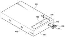
도 6은 본 발명의 제1 실시예에 따른 액정 표시 장치에 포함되는 제2 수납 용기의 저면 사시도이다.6 is a bottom perspective view of a second storage container included in the liquid crystal display according to the first exemplary embodiment of the present invention.
도 7은 본 발명의 제1 실시예의 제2 수납 용기에 연성 인쇄회로기판이 배치되는 모습을 나타낸 개략도이다.FIG. 7 is a schematic view illustrating a flexible printed circuit board disposed in a second storage container according to a first embodiment of the present invention.
도 8은 본 발명의 제2 실시예에 따른 액정 표시 장치를 나타낸 분해 사시도이다.8 is an exploded perspective view illustrating a liquid crystal display according to a second exemplary embodiment of the present invention.
도 9는 본 발명의 제2 실시예에 따른 액정 표시 장치에 포함되는 제1 수납 용기의 저면 사시도이다.9 is a bottom perspective view of a first storage container included in a liquid crystal display according to a second exemplary embodiment of the present invention.
도 10은 본 발명의 제2 실시예의 제1 수납 용기에 연성 인쇄회로기판이 배치되는 모습을 나타낸 개략도이다.FIG. 10 is a schematic view illustrating a flexible printed circuit board disposed in a first accommodating container according to a second exemplary embodiment of the present invention.
도 11은 본 발명의 제2 실시예에 따른 액정 표시 장치에 포함되는 제2 수납 용기의 저면 사시도이다.11 is a bottom perspective view of a second storage container included in a liquid crystal display according to a second exemplary embodiment of the present invention.
도 12는 본 발명의 제2 실시예의 제2 수납 용기에 연성 인쇄회로기판이 배치되는 모습을 나타낸 개략도이다.FIG. 12 is a schematic view showing a flexible printed circuit board disposed in a second storage container according to a second embodiment of the present invention. FIG.
(도면의 주요부분에 대한 부호의 설명)DESCRIPTION OF THE REFERENCE NUMERALS (S)
111: 제1 표시판112: 제2 표시판111: first display panel 112: second display panel
113: 제1 편광판114: 제2 편광판113: first polarizing plate 114: second polarizing plate
115: 구동 집적회로120: 광학 시트115: drive integrated circuit 120: optical sheet
130: 도광판140: 반사 시트130: Light guide plate 140: Reflective sheet
150: 접착층200: 연성 인쇄회로기판150: adhesive layer 200: flexible printed circuit board
210: 연성 인쇄회로기판의 일측220: 연성 인쇄회로기판의 타측210: one side of the flexible printed circuit board 220: the other side of the flexible printed circuit board
225: 연성 인쇄회로기판의 연장부230: 커넥터 실장부225: extension portion of the flexible printed circuit board 230: connector mounting portion
240: 점광원250: 커넥터240: point light source 250: connector
260: 구동 부품300, 301: 제1 수납 용기260:
310: 안착단320, 321: 제1 수납 용기 제1 측벽310:
320a: 제1 가이드 홈330: 제1 수납 용기 제2 측벽320a: first guide groove 330: first storage container second sidewall
330a: 제2 가이드 홈340: 체결 돌기330a: second guide groove 340: fastening protrusion
350: 점광원 수납홈360: 구동 부품 수납홈350: point light source receiving groove 360: drive part receiving groove
400, 401: 제2 수납 용기410: 바닥판400, 401: second storage container 410: bottom plate
420, 421: 제2 수납 용기 측벽430, 431: 개구부420 and 421: second
440, 441: 커넥터 실장부 연결홈450: 체결홈440, 441: connector mounting connection groove 450: fastening groove
본 발명은 액정 표시 장치에 관한 것으로, 보다 상세하게는 이 장치에 포함되는 연성 인쇄회로기판(FPC: Flexible Printed Circuit)의 두께가 증가되어 제조 원가가 절감된 액정 표시 장치에 관한 것이다.BACKGROUND OF THE INVENTION 1. Field of the Invention The present invention relates to a liquid crystal display device, and more particularly, to a liquid crystal display device in which a manufacturing cost is reduced by increasing the thickness of a flexible printed circuit (FPC) included in the device.
액정 표시 장치(Liquid Crystal Display : LCD)는 현재 가장 널리 사용되고 있는 평판 표시 장치(Flat Panel Display : FPD) 중 하나로서, 전극이 형성되어 있는 두 장의 기판과 그 사이에 삽입되어 있는 액정층으로 이루어져, 전극에 전압을 인가하여 액정층의 액정 분자들을 재배열시킴으로써 투과되는 빛의 양을 조절하는 표시 장치로서, 소형화, 경량화 및 저전력 소비화 등의 이점을 가지고 있다.Liquid crystal display (LCD) is one of the most widely used flat panel display (FPD), and consists of two substrates on which electrodes are formed and a liquid crystal layer interposed therebetween. A display device that controls the amount of light transmitted by rearranging liquid crystal molecules of a liquid crystal layer by applying a voltage to an electrode, has advantages such as miniaturization, light weight, and low power consumption.
액정 표시 장치는 이를 필요로 하는 휴대폰 및 PDA(portable digital assistor) 등과 같은 소형 제품인 뿐만 아니라 중대형 제품인 모니터 및 TV 등에도 장착되어 사용되는 등 표시 장치가 필요한 거의 모든 정보 처리 기기에 장착되어 사용되고 있다.The liquid crystal display device is not only a small product such as a mobile phone and a portable digital assistor (PDA) that require it, but is also used in almost all information processing devices requiring a display device such as being used in a monitor and a TV, which are medium and large products.
액정 표시 장치는, 외부 전원을 인가받고 상하 기판에 신호를 전달하는 연성 인쇄회로기판을 구비하는데, 이러한 연성 인쇄회로기판은 고가이며, 두께가 얇을수록 제조 비용이 상승한다.The liquid crystal display device includes a flexible printed circuit board that receives an external power source and transmits a signal to the upper and lower substrates. The flexible printed circuit board is expensive, and the thinner the thickness, the higher the manufacturing cost.
액정 표시 장치는 최근 경박단소화 및 제조 원가 절감에 대한 요구에 직면하고 있으며, 휴대폰과 같은 소형 제품에 사용되는 액정 표시 장치에서는 이러한 요구가 절실하다.Liquid crystal display devices are recently faced with the demand for reducing the size and manufacturing cost, and the need for such a liquid crystal display device used in small products such as mobile phones.
따라서, 가능한 두꺼운 연성 인쇄회로기판을 사용하면서도, 전체 두께는 증가하지 않는 액정 표시 장치가 요구된다.Accordingly, there is a need for a liquid crystal display device that uses the thickest flexible printed circuit board as possible but does not increase the overall thickness.
본 발명이 이루고자 하는 기술적 과제는, 연성 인쇄회로기판의 두께가 증가되어 제조 원가가 절감된 액정 표시 장치를 제공하고자 하는 것이다.An object of the present invention is to provide a liquid crystal display device in which the thickness of a flexible printed circuit board is increased and manufacturing cost is reduced.
본 발명의 기술적 과제들은 이상에서 언급한 기술적 과제로 제한되지 않으며, 언급되지 않은 또 다른 기술적 과제들은 아래의 기재로부터 당업자에게 명확하게 이해될 수 있을 것이다.The technical objects of the present invention are not limited to the technical matters mentioned above, and other technical subjects not mentioned can be clearly understood by those skilled in the art from the following description.
상기 기술적 과제를 달성하기 위한 본 발명의 일 실시예에 따른 액정 표시 장치는, 액정 패널과, 상부로부터 상기 액정 패널이 수납되고, 복수의 제1 수납 용기 측벽을 포함하는 제1 수납 용기와, 상기 제1 수납 용기의 하부에 배치되는 반사 시트와, 일측이 상기 액정 패널에 접촉되고, 타측이 상기 제1 수납 용기의 하부에 배치되는 연성 인쇄회로기판과, 상기 반사 시트가 부착되는 바닥판, 상기 바닥판의 가장자리를 따라 배치되어 상기 제1 수납 용기와 체결되는 제2 수납 용기 측벽, 및 상기 연성 인쇄회로기판을 노출시키도록 상기 바닥판에 형성된 개구부를 포함하는 제2 수납 용기를 포함한다.According to an aspect of the present invention, there is provided a liquid crystal display device comprising: a liquid crystal panel; a first storage container in which the liquid crystal panel is received from an upper portion; and a plurality of first storage container sidewalls; A reflective sheet disposed under the first storage container, a flexible printed circuit board having one side contacting the liquid crystal panel and the other side disposed under the first storage container, a bottom plate to which the reflective sheet is attached, and A second storage container including a second storage container sidewall disposed along an edge of the bottom plate and coupled to the first storage container, and an opening formed in the bottom plate to expose the flexible printed circuit board.
상기 기술적 과제를 달성하기 위한 본 발명의 다른 실시예에 따른 액정 표시 장치는, 액정 패널과, 상부로부터 상기 액정 패널이 수납되고, 복수의 제1 수납 용기 측벽을 포함하는 제1 수납 용기와, 상기 제1 수납 용기의 하부에 배치되는 반사 시트와, 일측이 상기 액정 패널에 접촉되고, 타측이 상기 제1 수납 용기의 하부에 배치되는 연성 인쇄회로기판과, 상기 반사 시트가 부착되는 바닥판, 상기 바닥판의 가장자리를 따라 배치되어 상기 제1 수납 용기와 체결되는 제2 수납 용기 측벽, 및 상기 연성 인쇄회로기판을 노출시키도록 상기 바닥판으로부터 상기 제2 수납 용기 측벽까지 연장되어 형성된 개구부를 포함하는 제2 수납 용기를 포함한다.According to another aspect of the present invention, there is provided a liquid crystal display device comprising: a liquid crystal panel; a first storage container in which the liquid crystal panel is received from an upper portion; and a plurality of first storage container sidewalls; A reflective sheet disposed under the first storage container, a flexible printed circuit board having one side contacting the liquid crystal panel and the other side disposed under the first storage container, a bottom plate to which the reflective sheet is attached, and A second accommodating container sidewall disposed along an edge of the bottom plate and fastened to the first accommodating container, and an opening extending from the bottom plate to the second accommodating container sidewall to expose the flexible printed circuit board. And a second storage container.
본 발명의 이점 및 특징, 그리고 그것들을 달성하는 방법은 첨부되는 도면과 함께 상세하게 후술되어 있는 실시예들을 참조하면 명확해질 것이다. 그러나 본 발명은 이하에서 개시되는 실시예들에 한정되는 것이 아니라 서로 다른 다양한 형태로 구현될 수 있으며, 단지 본 실시예들은 본 발명의 개시가 완전하도록 하고, 본 발명이 속하는 기술분야에서 통상의 지식을 가진 자에게 발명의 범주를 완전하게 알려주기 위해 제공되는 것이며, 본 발명은 청구항의 범주에 의해 정의될 뿐이다. 명세서 전체에 걸쳐 동일 참조 부호는 동일 구성 요소를 지칭한다.Advantages and features of the present invention and methods for achieving them will be apparent with reference to the embodiments described below in detail with the accompanying drawings. The present invention may, however, be embodied in many different forms and should not be construed as limited to the embodiments set forth herein. Rather, these embodiments are provided so that this disclosure will be thorough and complete, and will fully convey the scope of the invention to those skilled in the art. To fully disclose the scope of the invention to those skilled in the art, and the invention is only defined by the scope of the claims. Like reference numerals refer to like elements throughout.
이하 첨부된 도면을 참조하여 본 발명의 실시예들을 상세히 설명한다.Hereinafter, embodiments of the present invention will be described in detail with reference to the accompanying drawings.
도 1 및 도 2를 참조하여, 본 발명의 일 실시예에 따른 액정 표시 장치에 대하여 상세히 설명한다. 도 1은 본 발명의 제1 실시예에 따른 액정 표시 장치를 나 타낸 분해 사시도이다. 도 2는 도 1의 A-A'선을 따라 액정 표시 장치를 자른 단면도이다.1 and 2, a liquid crystal display according to an exemplary embodiment of the present invention will be described in detail. 1 is an exploded perspective view illustrating a liquid crystal display according to a first embodiment of the present invention. FIG. 2 is a cross-sectional view of the liquid crystal display taken along the line AA ′ of FIG. 1.
도 1을 참조하면, 본 발명의 일 실시예에 따른 액정 표시 장치는 전체적으로 액정 패널(110), 광학 시트(120), 도광판(130), 반사 시트(140), 접착층(150), 연성 인쇄회로기판(200), 제1 수납 용기(300) 및 제2 수납 용기(400)를 포함한다.Referring to FIG. 1, the liquid crystal display according to the exemplary embodiment of the present invention generally includes a
액정 패널(110)은 게이트 라인(미도시) 및 데이터 라인(미도시)과 박막 트랜지스터 어레이, 화소 전극 등을 포함하는 제1 표시판(111)과, 블랙 매트릭스(black matrix), 공통 전극 등을 포함하고 제1 표시판(111)에 대향하도록 배치된 제2 표시판(112), 제1 표시판(111) 하부에 배치된 제1 편광판(113)과 제2 표시판(112) 상부에 배치된 제2 편광판(114)을 포함한다. 제1 표시판(111)과 제2 표시판(112) 사이에는 액정층(미도시)이 개재된다.The
액정 패널(110)은 상술한 평판 형상의 기판들이 적층되어, 후술하는 제1 수납 용기(300)에 배치된다. 구체적으로, 액정 패널(110)은, 제1 수납 용기(300)의 상부로부터 수납되어 안착단(310)에 배치될 수 있다. 액정 패널(110)의 일측에는 액정 표시 장치를 구동하기 위한 구동 집적회로(driver Integrated circuit)(115) 및 연성 인쇄회로기판(200)이 배치될 수 있다. 구동 집적회로(115)는 연성 인쇄회로기판(200)으로부터 구동 전원을 인가받을 수 있도록 연성 인쇄회로기판(200)과 전기적으로 연결되어 있다.The
액정 패널(110) 하부에는 광학 시트(120)가 배치된다. 광학 시트(120)는 점광원(250)으로부터 전달되어 도광판(130)을 통과한 광을 확산하고 집광하는 역할을 한다. 광학 시트(120)는 확산 시트(diffusion sheet)(121), 제1 프리즘 시트(122), 제2 프리즘 시트(123) 등을 포함한다.The
여기서 확산 시트(121)는 도광판(130) 상부에 위치하고 점광원(250)으로부터 입사되는 광의 휘도 및 휘도 균일성을 향상시키는 역할을 한다.The
확산 시트(121) 상부에는 확산 시트(121)로부터 확산된 광을 집광하고 출사시키는 제1 프리즘 시트(122) 및 제2 프리즘 시트(123)가 위치한다. 다만 제1 프리즘 시트(122)만으로도 휘도 및 시야각을 충분히 확보할 수 있는 경우 제2 프리즘 시트(123)는 제외될 수 있다.The
본 실시예의 광학 시트(120)는 액정 패널(110)과 함께 제1 수납 용기(300)에 수납된다. 즉, 광학 시트(120)는 도광판(130) 상부에 배치되어 액정 패널(110)과 직접 접촉할 수 있다. 이와 달리 광학 시트(120)는 제1 수납 용기(300)에 별도로 구비된 분리단(미도시)에 의해 액정 패널(110)과 분리될 수도 있다.The
이하, 도 1 및 도 3을 참조하여 본 발명의 제1 실시예에 따른 액정 표시 장치에 포함되는 연성 인쇄회로기판에 대하여 상세히 설명한다. 도 3은 본 발명의 제1 실시예에 따른 액정 표시 장치에 포함되는 연성 인쇄회로기판의 저면 사시도이다.Hereinafter, a flexible printed circuit board included in a liquid crystal display according to a first exemplary embodiment of the present invention will be described in detail with reference to FIGS. 1 and 3. 3 is a bottom perspective view of a flexible printed circuit board included in a liquid crystal display according to a first exemplary embodiment of the present invention.
도 1 내지 도 3을 참조하면, 연성 인쇄회로기판(200)의 일측(210)은 액정 패널(110), 구체적으로는 제1 표시판(111)에 접촉된다. 연성 인쇄회로기판(200)은 후술하는 제1 수납 용기 측벽(320, 330), 구체적으로는 제1 수납 용기(300)의 제1 가이드 홈(320a)을 따라 절곡되어, 연성 인쇄회로기판(200)의 타측(220)이 제1 수납 용기(300)의 안착단(310)의 하면측에 부착된다.1 to 3, one
도시하지는 않았지만, 연성 인쇄회로기판(200)의 타측(220)의 가장자리는 양면 테이프 등 접착층(미도시)이 형성될 수 있으며, 이 접착층에 의해 연성 인쇄회로기판(200)의 타측(220)이 제1 수납 용기(300)에 부착될 수 있다. 연성 인쇄회로기판(200)의 타측(220)에는 게이트 구동 신호 및 데이터 구동 신호를 인가하도록 하는 게이트 구동신호 및 데이터 구동신호를 모두 처리하기 위한 여러 구동 부품(260)이 실장된다.Although not shown, an edge of the
또한 연성 인쇄회로기판(200)에는 수동 발광 장치인 액정 표시 장치에 광을 제공하는 점광원(240)이 실장된다. 연성 인쇄회로기판(200)은 연성 인쇄회로기판(200)의 타측(220)으로부터 연장된 연장부(225), 및 연장부(225)와 연결된 커넥터 실장부(230)를 더 포함할 수 있다. 연성 인쇄회로기판(200)이 타측(220)으로부터 수직 방향으로부터 연장된 연장부(225)를 포함하여, 연성 인쇄회로기판(200)은 전체적으로 'ㄷ'자 형상을 가질 수 있다.In addition, the flexible printed
연성 인쇄회로기판(200)은 소정 두께(T1)를 가지는 필름으로 이루어져 있으며, 필름의 두께(T1)가 얇을수록 제조 원가가 고가이다. 따라서 연성 인쇄회로기판(200)의 두께(T1)가 두꺼울수록 제조 원가를 절감할 수 있다. 연성 인쇄회로기판(200)의 타측(220)이 후술하는 반사 시트(140)와 중첩되지 않도록 연성 인쇄회로기판(200)의 길이(L1)를 조절함으로써 연성 인쇄회로기판(200)의 두께(T1)가 증가하더라도 액정 표시 장치 전체의 두께는 증가하지 않게 할 수 있다. 이와 같이 연성 인쇄회로기판(200)의 길이(L1)를 조절하면, 연성 인쇄회로기판(200)이 반사 시트(140) 및 반사 시트(140)를 제2 수납 용기(400)에 부착시키는 접착층(150) 등과 중첩되지 않는다. 이에 따라 연성 인쇄회로기판(200)이 반사 시트(140) 등과 중첩되도록 배치된 경우에 비해 연성 인쇄회로기판(200)의 두께(T1)가 증가되더라도 액정 표시 장치 전체의 두께는 증가하지 않는다.The flexible printed
연성 인쇄회로기판(200)의 타측(220)에 배치된 점광원(250)으로는 예를 들어 LED(Light Emitted Diode)를 사용할 수 있다. 점광원(240)은 후술하는 도광판(130)의 측벽에 평행하게 배치되어 도광판(130)에 광을 전달한다. 또한 연성 인쇄회로기판(200)의 커넥터 실장부(230)에 실장된 커넥터(250)는 외부로부터 전원을 인가하는 역할을 한다.For example, a light emitting diode (LED) may be used as the point
이하, 도 1, 도 4 및 도 5를 참조하여, 본 발명의 제1 실시예에 따른 제1 수납 용기에 대하여 상세히 설명한다. 도 4는 본 발명의 제1 실시예에 따른 액정 표시 장치에 포함되는 제1 수납 용기의 저면 사시도이다. 도 5는 본 발명의 제1 실시예의 제1 수납 용기에 연성 인쇄회로기판이 배치되는 모습을 나타낸 개략도이다.Hereinafter, a first storage container according to a first embodiment of the present invention will be described in detail with reference to FIGS. 1, 4, and 5. 4 is a bottom perspective view of a first accommodating container included in a liquid crystal display according to a first exemplary embodiment of the present invention. FIG. 5 is a schematic view showing a flexible printed circuit board disposed in a first accommodating container according to a first embodiment of the present invention.
제1 수납 용기(300)는 복수의 제1 수납 용기 측벽(320, 330)을 포함하는 틀 형상(frame shape)을 가질 수 있다. 제1 수납 용기(300)는 예를 들어 사각틀 형상일 수 있다. 이 경우 제1 수납 용기 측벽(320, 330)은 제1 수납 용기(300)의 가로 방향에 형성된 제1 수납 용기 제1 측벽(320) 및 세로 방향에 형성되어 제1 수납 용기 제1 측벽(320)에 이웃하는 제1 수납 용기 제2 측벽(330)으로 이루어진다. 제1 수납 용기(300)는 예를 들어 반사성 및 가공성이 양호한 백색 플라스틱으로 이루어질 수 있다. 제1 수납 용기(300)가 백색으로 이루어져 있어, 도광판(130)을 통과한 광이 제1 수납 용기(300)의 제1 수납 용기 측벽(320, 330)에서 반사되어 광의 손실을 최소화할 수 있다. 또한, 제1 수납 용기(300)가 플라스틱으로 이루어져 있어, 후술하는 안착단(310), 제1 가이드 홈(320a) 및 제2 가이드 홈(330a) 등을 형성하기 용이하다.The
제1 수납 용기 제1 측벽(320) 중 어느 하나에는 연성 인쇄회로기판(200)이 절곡되어 가이드되도록 제1 가이드 홈(320a)이 구비되어 있다. 제1 가이드 홈(320a)은 제1 수납 용기 제1 측벽(320)의 높이와 두께가 감소되도록 제1 수납 용기 제1 측벽(320)을 조각하여 형성할 수 있다. 제1 가이드 홈(320a)은 제1 수납 용기 제1 측벽(320)보다 높이 및 두께가 감소되어 있으므로, 연성 인쇄회로기판(200)의 일측(210)이 제1 가이드 홈(320a)을 따라 배치되는 경우 제1 수납 용기(300)의 외부로 돌출된 연성 인쇄회로기판(200)의 두께를 감소시킬 수 있다. 제1 가이드 홈(320a)은 후술하는 제2 수납 용기(400)의 개구부(430)와 중첩되어 연성 인쇄회로기판(200)이 개구부(440)에 수용된다. 이에 따라 연성 인쇄회로기판(200)의 타측은 후술하는 제2 수납 용기(400)의 바닥판(410)과 중첩되지 않는다.One of the first storage container first sidewalls 320 is provided with a
한편, 제1 수납 용기(300)는 제1 수납 용기 측벽(320, 330)의 내측을 따라 형성된 안착단(310)을 더 포함한다. 즉, 제1 수납 용기 측벽(320, 330)에 의해 정의된 제1 수납 용기(300)의 중앙부는 개방되어 있으며, 안착단(310)은 제1 수납 용기 측벽(320, 330)으로부터 제1 수납 용기(300)의 중앙부측으로 돌출된다. 안착 단(310)의 상부에는 상술한 바와 같이 액정 패널(110) 및 광학 시트(120)가 배치될 수 있다. 이와 달리, 광학 시트(120)는 상기 액정 패널(120)에 부착되어 안착단(310)의 일측에 배치될 수도 있다. 제1 가이드 홈(320a)에 인접하도록 배치된 안착단(310)의 일측은 그 폭이 중앙부측으로 확장되어 있다. 폭이 확장된 안착단(310)의 하면측에는 점광원 수납홈(350) 및 구동 부품 수납홈(360)이 형성되어 연성 인쇄회로기판(200)의 타측(220)에 실장된 점광원(240) 및 구동 부품(260)을 수납한다.Meanwhile, the
제1 수납 용기 제2 측벽(330)은 예를 들어 제1 수납 용기 제1 측벽(320)과 직교하도록 형성될 수 있다. 제1 수납 용기 제2 측벽(330)은 연성 인쇄회로기판(200)의 연장부(225)가 절곡되어 가이드되는 제2 가이드 홈(330a)을 구비한다. 연성 인쇄회로기판(200)의 연장부(225)는 화살표 방향으로 절곡되어 연성 인쇄회로기판(200)의 일측(210)과 중첩되며, 커넥터(250)는 제1 수납 용기(300)의 하면측을 향하게된다. 제2 가이드 홈(330a)은 후술하는 제2 수납 용기(400)의 개구부(430)와 중첩되도록 형성되어 연성 인쇄회로기판(200)이 개구부(430)에 수용된다. 이에 따라 연성 인쇄회로기판(200)이 제2 수납 용기(400)의 바닥판(410)과 중첩되지 않는다. 한편 제1 수납 용기 제2 측벽(330)에는 체결 돌기(340)가 구비되어 있으며, 이 체결 돌기(340)에 의해 제1 수납 용기(300)가 제2 수납 용기(400)와 체결된다.The first storage container
이하, 도 1, 도 2, 도 6 및 도 7을 참조하여 본 발명의 제1 실시예에 따른 액정 표시 장치에 포함되는, 도광판, 반사 시트, 접착층 및 제2 수납 용기에 대하여 상세히 설명한다. 도 6은 본 발명의 제1 실시예에 따른 액정 표시 장치에 포함 되는 제2 수납 용기의 저면 사시도이다. 도 7은 본 발명의 제1 실시예의 제2 수납 용기에 연성 인쇄회로기판이 배치되는 모습을 나타낸 개략도이다.Hereinafter, a light guide plate, a reflective sheet, an adhesive layer, and a second storage container included in the liquid crystal display according to the first embodiment of the present invention will be described in detail with reference to FIGS. 1, 2, 6, and 7. 6 is a bottom perspective view of a second accommodating container included in the liquid crystal display according to the first exemplary embodiment of the present invention. FIG. 7 is a schematic view illustrating a flexible printed circuit board disposed in a second storage container according to a first embodiment of the present invention.
도광판(130)은 제1 수납 용기(300)의 하부에 배치되어, 점광원(240)으로부터 출사된 광을 가이드하는 역할을 한다. 도광판(130)은 광이 효율적으로 가이드될 수 있도록 투광성을 가지는 재료, 예를 들어 PMMA(PolyMethyl MethAcrylate)와 같은 아크릴 수지, 폴리카보네이트(PC: PolyCarbonate)와 같은 일정한 굴절율을 가지는 재료로 이루어질 수 있다. 도광판(130)의 일면에는 도광판(130)의 일측으로부터 도광판(130) 내부로 전달된 광이 상부로 출사될 수 있도록 산란 패턴(미도시)이 형성될 수 있다.The
도광판(130)의 하부에는 반사 시트(140)가 배치되며, 반사 시트(140)는 제2 수납 용기(400)측으로 방출되는 광을 상부로 반사시킨다.The
반사 시트(140)의 하부에는 접착층(150)이 배치되며, 접착층(150)은 반사 시트(140)를 제2 수납 용기(400)의 바닥판(410)에 부착시킨다. 접착층(150)은 예를 들어 양면 테이프일 수 있다.An
제2 수납 용기(400)는 도광판(130), 반사 시트(140) 등을 수납하며, 제1 수납 용기(300)와 체결된다. 제2 수납 용기(400)는 액정 표시 장치의 최하부에 배치되어 수납된 부품들을 보호하도록 금속으로 이루어질 수 있으며, "바텀 샤시"라고도 한다.The
제2 수납 용기(400)는 반사 시트(140)가 부착되는 바닥판(410), 바닥판(410)의 가장자리를 따라 배치되어 제1 수납 용기(300)와 체결되는 제2 수납 용기 측 벽(420)을 포함한다.The
바닥판(410)은 소정 두께(T4)를 가질 수 있으며, 바닥판(410)에 반사 시트(140)가 부착되고 도광판(130) 등이 지지된다.The
바닥판(410)의 일측에는 개구부(430)가 형성되어 있다. 개구부(430)는 바닥판(410)의 일부를 절개하여 형성되며, 연성 인쇄회로기판(200)의 타측(220)이 개구부(430)로 노출된다. 연성 인쇄회로기판(200)의 타측(220)은 제1 수납 용기(300)의 하부에 배치되고 반사 시트(140) 및 접착층(150)과 중첩되지 않으므로 연성 인쇄회로기판(200)의 두께(T1)가 증가될 수 있는 점은 상술하였다. 이에 더하여, 제2 수납 용기(400)에 개구부(430)를 형성함으로써 연성 인쇄회로기판(200)이 제2 수납 용기(400)와 중첩되지 않으며, 이에 따라 연성 인쇄회로기판(200)의 두께(T1)를 보다 증가시킬 수 있다. 즉, 도 2에 도시된 바와 같이 연성 인쇄회로기판(200)의 두께(T1)는 연성 인쇄회로기판(200)이 제2 수납 용기(400)의 바닥판(410)의 외부로 돌출되지 않는 두께(T1)를 가질 수 있다. 이 경우 연성 인쇄회로기판(200)의 두께(T1)는 반사 시트(140)의 두께(T2), 접착층(150)의 두께(T3) 및 바닥판(410)의 두께(T4)의 합과 같거나 이보다 작을 수 있다. 연성 인쇄회로기판(200)이 제2 수납 용기(400)에 배치되어 개구부(430)에 수용된 경우 제2 수납 용기(400)의 바닥판(410)의 외면과 연성 인쇄회로기판(200)의 타측(220)은 소정 두께(T5)만큼 이격되어 있을 수 있다. 이와 같이 제2 수납 용기(400)에 개구부(430)가 형성됨으로써 연성 인쇄회로기판(200)의 두께(T1)가 보다 증가될 수 있으며, 이에 따라 고가의 연성 인쇄회로기판(200)의 제조 원가를 절감할 수 있다. 또한, 개구부(430)가 형성되어 있어, 제2 수납 용기(400)에 연성 인쇄회로기판(200)을 고정시키기 위한 접착층이 요구되지 않으므로 접착에 소요되는 비용도 절감할 수 있다.An
한편, 제2 수납 용기(400)의 바닥판(410)의 가장 자리에는 제2 수납 용기 측벽(420)들이 형성되어 수납 공간을 정의한다. 제2 수납 용기 측벽(420) 일측에는 연성 인쇄회로기판(200)의 커넥터 실장부(230)가 제2 수납 용기(400)의 내부로부터 외부로 인출되도록 커넥터 실장부 연결홈(440)이 구비되어 있다. 이에 따라 연성 인쇄회로기판(200)에 실장된 커넥터(250)는 제2 수납 용기(400)의 외부로 노출되어 외부 전원을 인가받아 액정 표시 장치를 구동시킨다. 또한, 제2 수납 용기 측벽(420)에는 제1 수납 용기(300)와 체결되도록 체결홈(450)이 구비될 수 있다. 체결홈(450)은 제1 수납 용기(300)의 체결 돌기(340)와 체결된다.Meanwhile, second
이상 설명한 액정 표시 장치의 상부, 즉 액정 패널(110)의 상부에는 탑 샤시(미도시)에 의해 보호되거나, 휴대폰과 같은 장치에 사용되는 경우 탑 샤시가 생략되고 별도의 보호 덮개에 의해 보호될 수도 있다.The upper chassis of the liquid crystal display device described above, that is, the upper portion of the
이하, 도 8 내지 도 10을 참조하여, 본 발명의 제2 실시예에 따른 액정 표시 장치에 대하여 상세히 설명한다. 도 8은 본 발명의 제2 실시예에 따른 액정 표시 장치를 나타낸 분해 사시도이다. 도 9는 본 발명의 제2 실시예에 따른 액정 표시 장치에 포함되는 제1 수납 용기의 저면 사시도이다. 도 10은 본 발명의 제2 실시예 의 제1 수납 용기에 연성 인쇄회로기판이 배치되는 모습을 나타낸 개략도이다. 설명의 편의상, 상기 일 실시예의 도면에 나타낸 각 부재와 동일 기능을 갖는 부재는 동일 부호로 나타내고, 따라서 그 설명은 생략한다. 본 실시예에 따른 액정 표시 장치는 제1 및 제2 수납 용기의 구조 및 연성 인쇄회로기판의 길이가 일부 상이한 점을 제외하고는 본 발명의 제1 실시예에 따른 액정 표시 장치와 기본적으로 동일한 구조를 갖는다.Hereinafter, the liquid crystal display according to the second exemplary embodiment of the present invention will be described in detail with reference to FIGS. 8 to 10. 8 is an exploded perspective view illustrating a liquid crystal display according to a second exemplary embodiment of the present invention. 9 is a bottom perspective view of a first storage container included in a liquid crystal display according to a second exemplary embodiment of the present invention. FIG. 10 is a schematic view illustrating a flexible printed circuit board disposed in a first accommodating container according to a second exemplary embodiment of the present invention. For convenience of description, members having the same functions as the members shown in the drawings of the above embodiment are denoted by the same reference numerals, and thus description thereof is omitted. The liquid crystal display according to the present exemplary embodiment basically has the same structure as the liquid crystal display according to the first exemplary embodiment except that the structures of the first and second storage containers and the length of the flexible printed circuit board are partially different. Has
도 8 내지 도 10을 참조하면, 본 실시예의 제1 수납 용기(301)는 예를 들어 사각틀 형상을 가질 수 있으며, 복수의 제1 수납 용기 측벽(321, 330) 및 제1 수납 용기 측벽(321, 330)을 따라 형성된 안착단(310)을 포함한다. 제1 수납 용기 측벽(321, 330)은 제1 수납 용기 제1 측벽(321) 및 제1 수납 용기 제2 측벽(330)을 포함한다. 본 실시예의 제1 수납 용기 제1 측벽(321)에는 이전 실시예와 상이하게 가이드 홈이 형성되어 있지 않다. 이에 따라 제1 수납 용기(301)의 제작이 용이하다. 연성 인쇄회로기판(200)은 제1 수납 용기 제1 측벽(321)의 외측면을 따라 절곡된다. 이를 위해 연성 인쇄회로기판(200)의 길이(L2)는 이전 실시예보다 길게 형성될 수 있다. 제1 수납 용기 제1 측벽(321)에 인접한 제1 수납 용기 제2 측벽(330)은 연성 인쇄회로기판(200)의 연장부(225)가 절곡되어 가이드되는 제2 가이드 홈(330a)을 구비한다. 연성 인쇄회로기판(200)의 연장부(225)는 연성 인쇄회로기판(200)의 연장부(225)는 화살표 방향으로 절곡되어 연성 인쇄회로기판(200)의 일측(210)과 중첩된다. 제2 가이드 홈(330a)은 연성 인쇄회로기판(200)이 제1 수납 용기 제2 측벽(330) 외부로 연성 인쇄회로기판(200)이 지나치게 돌출되는 것을 방지한다. 제2 가이드 홈(330a)은 후술하는 개구부(431)와 중첩되어 연성 인쇄회로기판(200)이 개구부(431)에 수용된다.8 to 10, the
이하, 도 8, 도 11 및 도 12를 참조하여, 본 발명의 제2 실시예에 따른 제2 수납 용기에 대하여 상세히 설명한다. 도 11은 본 발명의 제2 실시예에 따른 액정 표시 장치에 포함되는 제2 수납 용기의 저면 사시도이다. 도 12는 본 발명의 제2 실시예의 제2 수납 용기에 연성 인쇄회로기판이 배치되는 모습을 나타낸 개략도이다.Hereinafter, with reference to FIGS. 8, 11 and 12, a second storage container according to a second embodiment of the present invention will be described in detail. 11 is a bottom perspective view of a second storage container included in a liquid crystal display according to a second exemplary embodiment of the present invention. FIG. 12 is a schematic view showing a flexible printed circuit board disposed in a second storage container according to a second embodiment of the present invention. FIG.
도 8, 도 11 및 도 12를 참조하면, 본 실시예의 제2 수납 용기(401)의 개구부(431)는 바닥판(410)으로부터 제2 수납 용기 측벽(420)까지 연장되어 형성된다. 제1 수납 용기(301)의 상부에 배치된 연성 인쇄회로기판(200)의 일측(210)을 제외한 부분은 개구부(431)에 수용되어 제2 수납 용기(401)의 바닥판(410) 및 제2 수납 용기 측벽(420)과 중첩되지 않는다. 따라서, 본 실시예의 연성 인쇄회로기판(200)도 반사 시트(140)와 중첩되지 않도록 제1 수납 용기(301)의 하면측에 배치되며, 개구부(431)에 의해 형성된 공간까지 고려하면, 연성 인쇄회로기판(200)의 두께(T1)는 증가할 수 있다. 이 경우 연성 인쇄회로기판(200)의 두께(T1)는 반사 시트(140)의 두께, 접착층(150)의 두께 및 바닥판(410)의 두께(T4)의 합과 같거나 작을 수 있다. 연성 인쇄회로기판(200)이 제2 수납 용기(401)에 배치되어 개구부(431)에 수용된 경우 제2 수납 용기(401)의 바닥판(410) 및 제2 수납 용기 측벽(420)의 외면과 연성 인쇄회로기판(200)의 타측(220)은 소정 두께(T5)만큼 이격되어 연성 인쇄회로기판(200)이 손상되는 것을 방지할 수 있다.8, 11, and 12, the
제2 수납 용기 측벽(420)측에 형성된 개구부(431)의 일측에는 연성 인쇄회로기판(200)의 커넥터 실장부(230)가 인출되는 커넥터 실장부 연결홈()이 구비되어 있다.One side of the
이상 첨부된 도면을 참조하여 본 발명의 실시예들을 설명하였지만, 본 발명이 속하는 기술분야에서 통상의 지식을 가진 자는 본 발명이 그 기술적 사상이나 필수적인 특징을 변경하지 않고서 다른 구체적인 형태로 실시될 수 있다는 것을 이해할 수 있을 것이다. 그러므로 이상에서 기술한 실시예들은 모든 면에서 예시적인 것이며 한정적이 아닌 것으로 이해해야만 한다.While the present invention has been described in connection with what is presently considered to be practical exemplary embodiments, it is to be understood that the invention is not limited to the disclosed embodiments, but, on the contrary, You will understand. It is therefore to be understood that the above-described embodiments are illustrative in all aspects and not restrictive.
상술한 바와 같이 본 발명의 실시예들에 따른 액정 표시 장치에 의하면, 다음과 같은 효과가 하나 혹은 그 이상 있다.As described above, according to the liquid crystal display according to the exemplary embodiments, there are one or more of the following effects.
첫째, 연성 인쇄회로기판을 반사 시트와 중첩되지 않도록 배치하여 액정 표시 장치의 두께 증가 없이 연성 인쇄회로기판의 두께를 증가시킬 수 있다.First, the flexible printed circuit board may be disposed not to overlap with the reflective sheet so that the thickness of the flexible printed circuit board may be increased without increasing the thickness of the liquid crystal display.
둘째, 제2 수납 용기에 개구부를 형성함으로써 액정 표시 장치의 두께 증가 없이 연성 인쇄회로기판의 두께를 증가시키는 한편, 연성 인쇄회로기판을 제2 수납 용기에 고정하기 위한 접착층을 생략할 수 있다.Second, by forming an opening in the second accommodating container, the thickness of the flexible printed circuit board may be increased without increasing the thickness of the liquid crystal display device, and an adhesive layer for fixing the flexible printed circuit board to the second accommodating container may be omitted.
셋째, 연성 인쇄회로기판의 두께를 증가시켜 액정 표시 장치의 제조 원가를 절감할 수 있다.Third, the manufacturing cost of the liquid crystal display may be reduced by increasing the thickness of the flexible printed circuit board.
Claims (24)
Translated fromKoreanPriority Applications (7)
| Application Number | Priority Date | Filing Date | Title |
|---|---|---|---|
| KR1020070055623AKR101348247B1 (en) | 2007-06-07 | 2007-06-07 | Liquid crystal display device |
| JP2007275277AJP5582677B2 (en) | 2007-06-07 | 2007-10-23 | Liquid crystal display |
| US12/148,342US7924389B2 (en) | 2007-06-07 | 2008-04-17 | Liquid crystal display with housing exposed flexible printed circuit |
| DE602008001460TDE602008001460D1 (en) | 2007-06-07 | 2008-05-29 | liquid-crystal display |
| EP08009790AEP2000849B1 (en) | 2007-06-07 | 2008-05-29 | Liquid crystal display |
| CN2008100859683ACN101320142B (en) | 2007-06-07 | 2008-06-06 | Liquid crystal display |
| US13/045,296US8848128B2 (en) | 2007-06-07 | 2011-03-10 | Liquid crystal display with housing exposed flexible printed circuit |
Applications Claiming Priority (1)
| Application Number | Priority Date | Filing Date | Title |
|---|---|---|---|
| KR1020070055623AKR101348247B1 (en) | 2007-06-07 | 2007-06-07 | Liquid crystal display device |
Publications (2)
| Publication Number | Publication Date |
|---|---|
| KR20080107633A KR20080107633A (en) | 2008-12-11 |
| KR101348247B1true KR101348247B1 (en) | 2014-01-09 |
Family
ID=39687065
Family Applications (1)
| Application Number | Title | Priority Date | Filing Date |
|---|---|---|---|
| KR1020070055623AExpired - Fee RelatedKR101348247B1 (en) | 2007-06-07 | 2007-06-07 | Liquid crystal display device |
Country Status (6)
| Country | Link |
|---|---|
| US (2) | US7924389B2 (en) |
| EP (1) | EP2000849B1 (en) |
| JP (1) | JP5582677B2 (en) |
| KR (1) | KR101348247B1 (en) |
| CN (1) | CN101320142B (en) |
| DE (1) | DE602008001460D1 (en) |
Families Citing this family (36)
| Publication number | Priority date | Publication date | Assignee | Title |
|---|---|---|---|---|
| JP4959506B2 (en)* | 2007-10-31 | 2012-06-27 | 株式会社ジャパンディスプレイイースト | Liquid crystal display |
| JP5287045B2 (en)* | 2008-08-29 | 2013-09-11 | サクサ株式会社 | Liquid crystal display |
| KR101515462B1 (en)* | 2008-11-13 | 2015-05-06 | 삼성디스플레이 주식회사 | Liquid crystal display device and method of assembling the same |
| US20110255251A1 (en)* | 2009-01-30 | 2011-10-20 | Sharp Kabushiki Kaisha | Electronic package and display apparatus |
| US8576209B2 (en)* | 2009-07-07 | 2013-11-05 | Semiconductor Energy Laboratory Co., Ltd. | Display device |
| JP5273804B2 (en)* | 2009-07-13 | 2013-08-28 | 株式会社ジャパンディスプレイ | Display device |
| CN101968579B (en)* | 2009-07-27 | 2013-01-02 | 群康科技(深圳)有限公司 | Liquid crystal display and assembling method thereof |
| KR101633105B1 (en)* | 2009-09-08 | 2016-06-24 | 엘지디스플레이 주식회사 | Liquid crystal display device |
| CN102062959B (en)* | 2009-11-12 | 2013-01-16 | 群康科技(深圳)有限公司 | Liquid crystal display unit |
| JP5377269B2 (en)* | 2009-12-22 | 2013-12-25 | 株式会社ジャパンディスプレイ | Electro-optical device and electronic apparatus |
| JP5507237B2 (en)* | 2009-12-25 | 2014-05-28 | 株式会社ジャパンディスプレイ | Liquid crystal display |
| TWI389067B (en)* | 2010-06-29 | 2013-03-11 | Compal Electronics Inc | Display module and assembly method thereof |
| KR101767961B1 (en)* | 2010-08-31 | 2017-08-16 | 삼성디스플레이 주식회사 | Light providing assembly and display device |
| KR101095122B1 (en)* | 2010-12-24 | 2011-12-16 | 삼성전기주식회사 | Laser navigation module |
| JP5655648B2 (en)* | 2011-03-15 | 2015-01-21 | 富士通株式会社 | Electronic device and circuit board connection structure |
| CN103364990A (en)* | 2012-03-30 | 2013-10-23 | 鑫成科技(成都)有限公司 | Liquid crystal display device |
| JP2014026173A (en)* | 2012-07-27 | 2014-02-06 | Japan Display Inc | Liquid crystal display device |
| KR102046864B1 (en) | 2013-03-13 | 2019-11-20 | 삼성전자주식회사 | Flexible display device |
| JP2014238497A (en)* | 2013-06-07 | 2014-12-18 | 株式会社ジャパンディスプレイ | Liquid crystal display device |
| KR102039363B1 (en)* | 2013-06-26 | 2019-11-01 | 엘지디스플레이 주식회사 | Liquid crystal display device |
| US20150153028A1 (en)* | 2013-07-25 | 2015-06-04 | Limited Liability Company "Dis Plus" | Housing for led lighting device |
| KR102098304B1 (en)* | 2013-12-10 | 2020-05-27 | 삼성디스플레이 주식회사 | Liquid crystal display and manufacturing method thereor |
| CN105531753B (en)* | 2014-09-02 | 2019-05-03 | 深圳市柔宇科技有限公司 | Display module and electronic device having the same |
| JP2017037140A (en)* | 2015-08-07 | 2017-02-16 | 株式会社ジャパンディスプレイ | Storage case and liquid crystal display device including the same |
| KR102331265B1 (en)* | 2015-08-31 | 2021-11-26 | 삼성디스플레이 주식회사 | Display device |
| KR102378723B1 (en)* | 2015-09-21 | 2022-03-28 | 삼성전자주식회사 | Display appartus |
| CN105785616A (en)* | 2016-05-05 | 2016-07-20 | 武汉华星光电技术有限公司 | Liquid crystal display device |
| RU2643526C2 (en) | 2016-05-17 | 2018-02-02 | Юрий Борисович Соколов | Led source of lighting with power supply from unstable tree-phase ac network |
| RU2633966C1 (en) | 2016-11-30 | 2017-10-20 | Юрий Борисович Соколов | Power supply from multi-phase alternating current network with correction of harmonic oscillations |
| EP3605206A4 (en) | 2017-04-17 | 2020-03-04 | Guangdong Oppo Mobile Telecommunications Corp., Ltd. | DISPLAY DEVICE, ELECTRONIC EQUIPMENT, AND PRODUCTION METHOD FOR A DISPLAY DEVICE |
| US10782736B2 (en)* | 2018-02-20 | 2020-09-22 | Intel Corporation | Edge-to-edge display devices and related methods |
| CN110012593A (en)* | 2019-04-18 | 2019-07-12 | 广西天山电子股份有限公司 | A flexible circuit board and preparation method thereof, and liquid crystal display module |
| US10895353B2 (en) | 2019-04-23 | 2021-01-19 | Lumileds Llc | Method of LED light engine assembly |
| KR102610045B1 (en)* | 2019-05-10 | 2023-12-06 | 엘지디스플레이 주식회사 | Display device |
| CN113946072B (en)* | 2021-10-28 | 2024-08-09 | 高创(苏州)电子有限公司 | Back panel, backlight module and display device |
| EP4328707A4 (en)* | 2021-11-29 | 2024-08-07 | Samsung Electronics Co., Ltd. | FLEXIBLE CIRCUIT BOARD CONNECTION ARRANGEMENT AND ELECTRONIC DEVICE THEREOF |
Citations (4)
| Publication number | Priority date | Publication date | Assignee | Title |
|---|---|---|---|---|
| JP2005017964A (en) | 2003-06-30 | 2005-01-20 | Kawaguchiko Seimitsu Co Ltd | Liquid crystal display device with back light |
| JP2005099619A (en) | 2003-09-26 | 2005-04-14 | Seiko Epson Corp | Electro-optical device and electronic apparatus including the electro-optical device |
| US20050179850A1 (en)* | 2004-02-12 | 2005-08-18 | Chang-Lung Du | Liquid crystal display module |
| JP2006038900A (en)* | 2004-07-22 | 2006-02-09 | Seiko Epson Corp | Electro-optical device and electronic apparatus |
Family Cites Families (26)
| Publication number | Priority date | Publication date | Assignee | Title |
|---|---|---|---|---|
| JP2868502B1 (en)* | 1998-02-12 | 1999-03-10 | 静岡日本電気株式会社 | LCD display module |
| JP3594500B2 (en)* | 1998-11-12 | 2004-12-02 | 松下電器産業株式会社 | LCD display mounting connection device |
| TWI304909B (en)* | 2000-10-04 | 2009-01-01 | Matsushita Electric Industrial Co Ltd | |
| US6930737B2 (en)* | 2001-01-16 | 2005-08-16 | Visteon Global Technologies, Inc. | LED backlighting system |
| KR100796487B1 (en)* | 2001-12-22 | 2008-01-21 | 엘지.필립스 엘시디 주식회사 | LCD Display |
| AU2002330309A1 (en)* | 2002-09-19 | 2004-04-08 | Matsushita Electric Industrial Co., Ltd. | Illumination unit and liquid crystal display comprising it |
| JP4345337B2 (en)* | 2003-03-31 | 2009-10-14 | セイコーエプソン株式会社 | Electro-optical device and electronic apparatus |
| JP4349009B2 (en)* | 2003-06-24 | 2009-10-21 | セイコーエプソン株式会社 | Electro-optical device, manufacturing method, and electronic apparatus |
| JP2005017791A (en)* | 2003-06-27 | 2005-01-20 | Hitachi Displays Ltd | Display device |
| TWI249717B (en)* | 2004-04-19 | 2006-02-21 | Au Optronics Corp | Signal transmission device |
| JP4468061B2 (en)* | 2004-04-30 | 2010-05-26 | 株式会社 日立ディスプレイズ | Display device |
| JP4196888B2 (en)* | 2004-06-25 | 2008-12-17 | セイコーエプソン株式会社 | Electro-optical device and electronic apparatus |
| KR101122216B1 (en)* | 2004-11-29 | 2012-03-19 | 삼성전자주식회사 | Backlight assembly and display apparatus having the same |
| JP4552637B2 (en)* | 2004-12-09 | 2010-09-29 | エプソンイメージングデバイス株式会社 | Liquid crystal display |
| KR20060070343A (en) | 2004-12-20 | 2006-06-23 | 삼성전자주식회사 | Flat panel display with integrated chassis |
| JP2006184383A (en)* | 2004-12-27 | 2006-07-13 | Seiko Epson Corp | Electro-optical device and electronic apparatus |
| JP4581726B2 (en)* | 2004-12-28 | 2010-11-17 | ソニー株式会社 | Display device and portable device |
| KR20060132202A (en)* | 2005-06-17 | 2006-12-21 | 삼성전자주식회사 | LCD Display |
| KR20070000073A (en) | 2005-06-27 | 2007-01-02 | 삼성전자주식회사 | Display device |
| JP4679985B2 (en)* | 2005-07-07 | 2011-05-11 | 株式会社 日立ディスプレイズ | Liquid crystal display device |
| JP4616105B2 (en)* | 2005-07-20 | 2011-01-19 | 株式会社 日立ディスプレイズ | Liquid crystal display device |
| TWI313374B (en)* | 2005-10-21 | 2009-08-11 | Innolux Display Corp | Liquid crystal display device |
| KR101266506B1 (en)* | 2005-12-08 | 2013-05-23 | 삼성디스플레이 주식회사 | Protecting cover used in display device and display device having the same |
| JP4238879B2 (en)* | 2006-04-03 | 2009-03-18 | エプソンイメージングデバイス株式会社 | Illumination device and liquid crystal display device |
| JP3129206U (en)* | 2006-11-27 | 2007-02-08 | 船井電機株式会社 | LCD module |
| TWM319423U (en)* | 2007-03-05 | 2007-09-21 | Innolux Display Corp | Liquid crystal display |
- 2007
- 2007-06-07KRKR1020070055623Apatent/KR101348247B1/ennot_activeExpired - Fee Related
- 2007-10-23JPJP2007275277Apatent/JP5582677B2/ennot_activeExpired - Fee Related
- 2008
- 2008-04-17USUS12/148,342patent/US7924389B2/enactiveActive
- 2008-05-29EPEP08009790Apatent/EP2000849B1/ennot_activeCeased
- 2008-05-29DEDE602008001460Tpatent/DE602008001460D1/enactiveActive
- 2008-06-06CNCN2008100859683Apatent/CN101320142B/ennot_activeExpired - Fee Related
- 2011
- 2011-03-10USUS13/045,296patent/US8848128B2/enactiveActive
Patent Citations (4)
| Publication number | Priority date | Publication date | Assignee | Title |
|---|---|---|---|---|
| JP2005017964A (en) | 2003-06-30 | 2005-01-20 | Kawaguchiko Seimitsu Co Ltd | Liquid crystal display device with back light |
| JP2005099619A (en) | 2003-09-26 | 2005-04-14 | Seiko Epson Corp | Electro-optical device and electronic apparatus including the electro-optical device |
| US20050179850A1 (en)* | 2004-02-12 | 2005-08-18 | Chang-Lung Du | Liquid crystal display module |
| JP2006038900A (en)* | 2004-07-22 | 2006-02-09 | Seiko Epson Corp | Electro-optical device and electronic apparatus |
Also Published As
| Publication number | Publication date |
|---|---|
| CN101320142A (en) | 2008-12-10 |
| JP2008304887A (en) | 2008-12-18 |
| CN101320142B (en) | 2012-08-29 |
| US20080303972A1 (en) | 2008-12-11 |
| KR20080107633A (en) | 2008-12-11 |
| US7924389B2 (en) | 2011-04-12 |
| JP5582677B2 (en) | 2014-09-03 |
| EP2000849A1 (en) | 2008-12-10 |
| US8848128B2 (en) | 2014-09-30 |
| DE602008001460D1 (en) | 2010-07-22 |
| EP2000849B1 (en) | 2010-06-09 |
| US20110164199A1 (en) | 2011-07-07 |
Similar Documents
| Publication | Publication Date | Title |
|---|---|---|
| KR101348247B1 (en) | Liquid crystal display device | |
| US8665389B2 (en) | Backlight assembly and liquid crystal display device including the same | |
| KR101621535B1 (en) | Backlight unit and liquid crystal display device having the same | |
| US9420714B2 (en) | Electronic device with unified display mounting structures | |
| US10180534B2 (en) | Borderless display device including display module | |
| US8031294B2 (en) | Liquid crystal display module | |
| KR101607572B1 (en) | Back-light assembly and display device having the same | |
| US7800707B2 (en) | Backlight module and liquid crystal display device using same | |
| US20080079863A1 (en) | Liquid Crystal Display Device | |
| US7377682B2 (en) | Backlight module and liquid crystal display device using the same | |
| US8432513B2 (en) | Liquid crystal display device | |
| US8696182B2 (en) | Display device and backlight unit for improving uniformity of brightness | |
| KR101929378B1 (en) | Liquid crystal display device | |
| KR20080028581A (en) | Light guide plate, backlight assembly and liquid crystal display device having same | |
| KR101824603B1 (en) | Backlight unit and liquid crystal display device and method having the same | |
| KR101737799B1 (en) | Light shielding tape and backlight unit using the same and liquid crystal display device having thereof | |
| JP2009238397A (en) | Illuminating device, liquid crystal device, and electronic equipment | |
| KR102575520B1 (en) | Liquid crystal display device | |
| KR20150049280A (en) | Liquid crystal display device and method for fabricating the same | |
| WO2012036040A1 (en) | Liquid crystal display device, liquid crystal panel, and flexible wiring substrate | |
| KR20070066709A (en) | Bidirectional backlight unit and liquid crystal display using the same | |
| KR20070114473A (en) | Display | |
| KR20070010584A (en) | Display device | |
| KR20070002505A (en) | LCD Display | |
| KR20160071490A (en) | Guide Panel And Backlight Unit Including Thereof |
Legal Events
| Date | Code | Title | Description |
|---|---|---|---|
| PA0109 | Patent application | St.27 status event code:A-0-1-A10-A12-nap-PA0109 | |
| PG1501 | Laying open of application | St.27 status event code:A-1-1-Q10-Q12-nap-PG1501 | |
| A201 | Request for examination | ||
| PA0201 | Request for examination | St.27 status event code:A-1-2-D10-D11-exm-PA0201 | |
| R18-X000 | Changes to party contact information recorded | St.27 status event code:A-3-3-R10-R18-oth-X000 | |
| N231 | Notification of change of applicant | ||
| PN2301 | Change of applicant | St.27 status event code:A-3-3-R10-R13-asn-PN2301 St.27 status event code:A-3-3-R10-R11-asn-PN2301 | |
| E902 | Notification of reason for refusal | ||
| PE0902 | Notice of grounds for rejection | St.27 status event code:A-1-2-D10-D21-exm-PE0902 | |
| E13-X000 | Pre-grant limitation requested | St.27 status event code:A-2-3-E10-E13-lim-X000 | |
| P11-X000 | Amendment of application requested | St.27 status event code:A-2-2-P10-P11-nap-X000 | |
| P13-X000 | Application amended | St.27 status event code:A-2-2-P10-P13-nap-X000 | |
| E701 | Decision to grant or registration of patent right | ||
| PE0701 | Decision of registration | St.27 status event code:A-1-2-D10-D22-exm-PE0701 | |
| GRNT | Written decision to grant | ||
| PR0701 | Registration of establishment | St.27 status event code:A-2-4-F10-F11-exm-PR0701 | |
| PR1002 | Payment of registration fee | St.27 status event code:A-2-2-U10-U11-oth-PR1002 Fee payment year number:1 | |
| PG1601 | Publication of registration | St.27 status event code:A-4-4-Q10-Q13-nap-PG1601 | |
| R18-X000 | Changes to party contact information recorded | St.27 status event code:A-5-5-R10-R18-oth-X000 | |
| PR1001 | Payment of annual fee | St.27 status event code:A-4-4-U10-U11-oth-PR1001 Fee payment year number:4 | |
| FPAY | Annual fee payment | Payment date:20171129 Year of fee payment:5 | |
| PR1001 | Payment of annual fee | St.27 status event code:A-4-4-U10-U11-oth-PR1001 Fee payment year number:5 | |
| FPAY | Annual fee payment | Payment date:20181126 Year of fee payment:6 | |
| PR1001 | Payment of annual fee | St.27 status event code:A-4-4-U10-U11-oth-PR1001 Fee payment year number:6 | |
| R18-X000 | Changes to party contact information recorded | St.27 status event code:A-5-5-R10-R18-oth-X000 | |
| FPAY | Annual fee payment | Payment date:20191202 Year of fee payment:7 | |
| PR1001 | Payment of annual fee | St.27 status event code:A-4-4-U10-U11-oth-PR1001 Fee payment year number:7 | |
| PC1903 | Unpaid annual fee | St.27 status event code:A-4-4-U10-U13-oth-PC1903 Not in force date:20201231 Payment event data comment text:Termination Category : DEFAULT_OF_REGISTRATION_FEE | |
| PC1903 | Unpaid annual fee | St.27 status event code:N-4-6-H10-H13-oth-PC1903 Ip right cessation event data comment text:Termination Category : DEFAULT_OF_REGISTRATION_FEE Not in force date:20201231 |