KR101346921B1 - A flat display device and method of manufacturing the same - Google Patents
A flat display device and method of manufacturing the sameDownload PDFInfo
- Publication number
- KR101346921B1 KR101346921B1KR1020080014899AKR20080014899AKR101346921B1KR 101346921 B1KR101346921 B1KR 101346921B1KR 1020080014899 AKR1020080014899 AKR 1020080014899AKR 20080014899 AKR20080014899 AKR 20080014899AKR 101346921 B1KR101346921 B1KR 101346921B1
- Authority
- KR
- South Korea
- Prior art keywords
- electrode
- region
- pixel
- gate
- flat panel
- Prior art date
- Legal status (The legal status is an assumption and is not a legal conclusion. Google has not performed a legal analysis and makes no representation as to the accuracy of the status listed.)
- Active
Links
Images


Classifications
- G—PHYSICS
- G02—OPTICS
- G02F—OPTICAL DEVICES OR ARRANGEMENTS FOR THE CONTROL OF LIGHT BY MODIFICATION OF THE OPTICAL PROPERTIES OF THE MEDIA OF THE ELEMENTS INVOLVED THEREIN; NON-LINEAR OPTICS; FREQUENCY-CHANGING OF LIGHT; OPTICAL LOGIC ELEMENTS; OPTICAL ANALOGUE/DIGITAL CONVERTERS
- G02F1/00—Devices or arrangements for the control of the intensity, colour, phase, polarisation or direction of light arriving from an independent light source, e.g. switching, gating or modulating; Non-linear optics
- G02F1/01—Devices or arrangements for the control of the intensity, colour, phase, polarisation or direction of light arriving from an independent light source, e.g. switching, gating or modulating; Non-linear optics for the control of the intensity, phase, polarisation or colour
- G02F1/13—Devices or arrangements for the control of the intensity, colour, phase, polarisation or direction of light arriving from an independent light source, e.g. switching, gating or modulating; Non-linear optics for the control of the intensity, phase, polarisation or colour based on liquid crystals, e.g. single liquid crystal display cells
- G02F1/133—Constructional arrangements; Operation of liquid crystal cells; Circuit arrangements
- G02F1/1333—Constructional arrangements; Manufacturing methods
- G02F1/1343—Electrodes
- G—PHYSICS
- G02—OPTICS
- G02F—OPTICAL DEVICES OR ARRANGEMENTS FOR THE CONTROL OF LIGHT BY MODIFICATION OF THE OPTICAL PROPERTIES OF THE MEDIA OF THE ELEMENTS INVOLVED THEREIN; NON-LINEAR OPTICS; FREQUENCY-CHANGING OF LIGHT; OPTICAL LOGIC ELEMENTS; OPTICAL ANALOGUE/DIGITAL CONVERTERS
- G02F1/00—Devices or arrangements for the control of the intensity, colour, phase, polarisation or direction of light arriving from an independent light source, e.g. switching, gating or modulating; Non-linear optics
- G02F1/01—Devices or arrangements for the control of the intensity, colour, phase, polarisation or direction of light arriving from an independent light source, e.g. switching, gating or modulating; Non-linear optics for the control of the intensity, phase, polarisation or colour
- G02F1/13—Devices or arrangements for the control of the intensity, colour, phase, polarisation or direction of light arriving from an independent light source, e.g. switching, gating or modulating; Non-linear optics for the control of the intensity, phase, polarisation or colour based on liquid crystals, e.g. single liquid crystal display cells
- G02F1/133—Constructional arrangements; Operation of liquid crystal cells; Circuit arrangements
- G02F1/136—Liquid crystal cells structurally associated with a semi-conducting layer or substrate, e.g. cells forming part of an integrated circuit
- G02F1/1362—Active matrix addressed cells
- G02F1/136213—Storage capacitors associated with the pixel electrode
- B—PERFORMING OPERATIONS; TRANSPORTING
- B82—NANOTECHNOLOGY
- B82Y—SPECIFIC USES OR APPLICATIONS OF NANOSTRUCTURES; MEASUREMENT OR ANALYSIS OF NANOSTRUCTURES; MANUFACTURE OR TREATMENT OF NANOSTRUCTURES
- B82Y20/00—Nanooptics, e.g. quantum optics or photonic crystals
- G—PHYSICS
- G02—OPTICS
- G02F—OPTICAL DEVICES OR ARRANGEMENTS FOR THE CONTROL OF LIGHT BY MODIFICATION OF THE OPTICAL PROPERTIES OF THE MEDIA OF THE ELEMENTS INVOLVED THEREIN; NON-LINEAR OPTICS; FREQUENCY-CHANGING OF LIGHT; OPTICAL LOGIC ELEMENTS; OPTICAL ANALOGUE/DIGITAL CONVERTERS
- G02F1/00—Devices or arrangements for the control of the intensity, colour, phase, polarisation or direction of light arriving from an independent light source, e.g. switching, gating or modulating; Non-linear optics
- G02F1/01—Devices or arrangements for the control of the intensity, colour, phase, polarisation or direction of light arriving from an independent light source, e.g. switching, gating or modulating; Non-linear optics for the control of the intensity, phase, polarisation or colour
- G02F1/13—Devices or arrangements for the control of the intensity, colour, phase, polarisation or direction of light arriving from an independent light source, e.g. switching, gating or modulating; Non-linear optics for the control of the intensity, phase, polarisation or colour based on liquid crystals, e.g. single liquid crystal display cells
- G02F1/133—Constructional arrangements; Operation of liquid crystal cells; Circuit arrangements
- G02F1/136—Liquid crystal cells structurally associated with a semi-conducting layer or substrate, e.g. cells forming part of an integrated circuit
- G—PHYSICS
- G02—OPTICS
- G02F—OPTICAL DEVICES OR ARRANGEMENTS FOR THE CONTROL OF LIGHT BY MODIFICATION OF THE OPTICAL PROPERTIES OF THE MEDIA OF THE ELEMENTS INVOLVED THEREIN; NON-LINEAR OPTICS; FREQUENCY-CHANGING OF LIGHT; OPTICAL LOGIC ELEMENTS; OPTICAL ANALOGUE/DIGITAL CONVERTERS
- G02F1/00—Devices or arrangements for the control of the intensity, colour, phase, polarisation or direction of light arriving from an independent light source, e.g. switching, gating or modulating; Non-linear optics
- G02F1/01—Devices or arrangements for the control of the intensity, colour, phase, polarisation or direction of light arriving from an independent light source, e.g. switching, gating or modulating; Non-linear optics for the control of the intensity, phase, polarisation or colour
- G02F1/13—Devices or arrangements for the control of the intensity, colour, phase, polarisation or direction of light arriving from an independent light source, e.g. switching, gating or modulating; Non-linear optics for the control of the intensity, phase, polarisation or colour based on liquid crystals, e.g. single liquid crystal display cells
- G02F1/1306—Details
- G02F1/1309—Repairing; Testing
- G—PHYSICS
- G02—OPTICS
- G02F—OPTICAL DEVICES OR ARRANGEMENTS FOR THE CONTROL OF LIGHT BY MODIFICATION OF THE OPTICAL PROPERTIES OF THE MEDIA OF THE ELEMENTS INVOLVED THEREIN; NON-LINEAR OPTICS; FREQUENCY-CHANGING OF LIGHT; OPTICAL LOGIC ELEMENTS; OPTICAL ANALOGUE/DIGITAL CONVERTERS
- G02F1/00—Devices or arrangements for the control of the intensity, colour, phase, polarisation or direction of light arriving from an independent light source, e.g. switching, gating or modulating; Non-linear optics
- G02F1/01—Devices or arrangements for the control of the intensity, colour, phase, polarisation or direction of light arriving from an independent light source, e.g. switching, gating or modulating; Non-linear optics for the control of the intensity, phase, polarisation or colour
- G02F1/13—Devices or arrangements for the control of the intensity, colour, phase, polarisation or direction of light arriving from an independent light source, e.g. switching, gating or modulating; Non-linear optics for the control of the intensity, phase, polarisation or colour based on liquid crystals, e.g. single liquid crystal display cells
- G02F1/133—Constructional arrangements; Operation of liquid crystal cells; Circuit arrangements
- G02F1/1333—Constructional arrangements; Manufacturing methods
- G02F1/133388—Constructional arrangements; Manufacturing methods with constructional differences between the display region and the peripheral region
- G—PHYSICS
- G02—OPTICS
- G02F—OPTICAL DEVICES OR ARRANGEMENTS FOR THE CONTROL OF LIGHT BY MODIFICATION OF THE OPTICAL PROPERTIES OF THE MEDIA OF THE ELEMENTS INVOLVED THEREIN; NON-LINEAR OPTICS; FREQUENCY-CHANGING OF LIGHT; OPTICAL LOGIC ELEMENTS; OPTICAL ANALOGUE/DIGITAL CONVERTERS
- G02F1/00—Devices or arrangements for the control of the intensity, colour, phase, polarisation or direction of light arriving from an independent light source, e.g. switching, gating or modulating; Non-linear optics
- G02F1/01—Devices or arrangements for the control of the intensity, colour, phase, polarisation or direction of light arriving from an independent light source, e.g. switching, gating or modulating; Non-linear optics for the control of the intensity, phase, polarisation or colour
- G02F1/13—Devices or arrangements for the control of the intensity, colour, phase, polarisation or direction of light arriving from an independent light source, e.g. switching, gating or modulating; Non-linear optics for the control of the intensity, phase, polarisation or colour based on liquid crystals, e.g. single liquid crystal display cells
- G02F1/133—Constructional arrangements; Operation of liquid crystal cells; Circuit arrangements
- G02F1/1333—Constructional arrangements; Manufacturing methods
- G02F1/1335—Structural association of cells with optical devices, e.g. polarisers or reflectors
- G02F1/133553—Reflecting elements
- G—PHYSICS
- G02—OPTICS
- G02F—OPTICAL DEVICES OR ARRANGEMENTS FOR THE CONTROL OF LIGHT BY MODIFICATION OF THE OPTICAL PROPERTIES OF THE MEDIA OF THE ELEMENTS INVOLVED THEREIN; NON-LINEAR OPTICS; FREQUENCY-CHANGING OF LIGHT; OPTICAL LOGIC ELEMENTS; OPTICAL ANALOGUE/DIGITAL CONVERTERS
- G02F1/00—Devices or arrangements for the control of the intensity, colour, phase, polarisation or direction of light arriving from an independent light source, e.g. switching, gating or modulating; Non-linear optics
- G02F1/01—Devices or arrangements for the control of the intensity, colour, phase, polarisation or direction of light arriving from an independent light source, e.g. switching, gating or modulating; Non-linear optics for the control of the intensity, phase, polarisation or colour
- G02F1/13—Devices or arrangements for the control of the intensity, colour, phase, polarisation or direction of light arriving from an independent light source, e.g. switching, gating or modulating; Non-linear optics for the control of the intensity, phase, polarisation or colour based on liquid crystals, e.g. single liquid crystal display cells
- G02F1/133—Constructional arrangements; Operation of liquid crystal cells; Circuit arrangements
- G02F1/136—Liquid crystal cells structurally associated with a semi-conducting layer or substrate, e.g. cells forming part of an integrated circuit
- G02F1/13606—Liquid crystal cells structurally associated with a semi-conducting layer or substrate, e.g. cells forming part of an integrated circuit having means for reducing parasitic capacitance
- G—PHYSICS
- G02—OPTICS
- G02F—OPTICAL DEVICES OR ARRANGEMENTS FOR THE CONTROL OF LIGHT BY MODIFICATION OF THE OPTICAL PROPERTIES OF THE MEDIA OF THE ELEMENTS INVOLVED THEREIN; NON-LINEAR OPTICS; FREQUENCY-CHANGING OF LIGHT; OPTICAL LOGIC ELEMENTS; OPTICAL ANALOGUE/DIGITAL CONVERTERS
- G02F1/00—Devices or arrangements for the control of the intensity, colour, phase, polarisation or direction of light arriving from an independent light source, e.g. switching, gating or modulating; Non-linear optics
- G02F1/01—Devices or arrangements for the control of the intensity, colour, phase, polarisation or direction of light arriving from an independent light source, e.g. switching, gating or modulating; Non-linear optics for the control of the intensity, phase, polarisation or colour
- G02F1/13—Devices or arrangements for the control of the intensity, colour, phase, polarisation or direction of light arriving from an independent light source, e.g. switching, gating or modulating; Non-linear optics for the control of the intensity, phase, polarisation or colour based on liquid crystals, e.g. single liquid crystal display cells
- G02F1/133—Constructional arrangements; Operation of liquid crystal cells; Circuit arrangements
- G02F1/136—Liquid crystal cells structurally associated with a semi-conducting layer or substrate, e.g. cells forming part of an integrated circuit
- G02F1/1362—Active matrix addressed cells
- G02F1/136204—Arrangements to prevent high voltage or static electricity failures
- G—PHYSICS
- G02—OPTICS
- G02F—OPTICAL DEVICES OR ARRANGEMENTS FOR THE CONTROL OF LIGHT BY MODIFICATION OF THE OPTICAL PROPERTIES OF THE MEDIA OF THE ELEMENTS INVOLVED THEREIN; NON-LINEAR OPTICS; FREQUENCY-CHANGING OF LIGHT; OPTICAL LOGIC ELEMENTS; OPTICAL ANALOGUE/DIGITAL CONVERTERS
- G02F1/00—Devices or arrangements for the control of the intensity, colour, phase, polarisation or direction of light arriving from an independent light source, e.g. switching, gating or modulating; Non-linear optics
- G02F1/01—Devices or arrangements for the control of the intensity, colour, phase, polarisation or direction of light arriving from an independent light source, e.g. switching, gating or modulating; Non-linear optics for the control of the intensity, phase, polarisation or colour
- G02F1/13—Devices or arrangements for the control of the intensity, colour, phase, polarisation or direction of light arriving from an independent light source, e.g. switching, gating or modulating; Non-linear optics for the control of the intensity, phase, polarisation or colour based on liquid crystals, e.g. single liquid crystal display cells
- G02F1/133—Constructional arrangements; Operation of liquid crystal cells; Circuit arrangements
- G02F1/136—Liquid crystal cells structurally associated with a semi-conducting layer or substrate, e.g. cells forming part of an integrated circuit
- G02F1/1362—Active matrix addressed cells
- G02F1/136231—Active matrix addressed cells for reducing the number of lithographic steps
- G02F1/136236—Active matrix addressed cells for reducing the number of lithographic steps using a grey or half tone lithographic process
- G—PHYSICS
- G02—OPTICS
- G02F—OPTICAL DEVICES OR ARRANGEMENTS FOR THE CONTROL OF LIGHT BY MODIFICATION OF THE OPTICAL PROPERTIES OF THE MEDIA OF THE ELEMENTS INVOLVED THEREIN; NON-LINEAR OPTICS; FREQUENCY-CHANGING OF LIGHT; OPTICAL LOGIC ELEMENTS; OPTICAL ANALOGUE/DIGITAL CONVERTERS
- G02F1/00—Devices or arrangements for the control of the intensity, colour, phase, polarisation or direction of light arriving from an independent light source, e.g. switching, gating or modulating; Non-linear optics
- G02F1/01—Devices or arrangements for the control of the intensity, colour, phase, polarisation or direction of light arriving from an independent light source, e.g. switching, gating or modulating; Non-linear optics for the control of the intensity, phase, polarisation or colour
- G02F1/165—Devices or arrangements for the control of the intensity, colour, phase, polarisation or direction of light arriving from an independent light source, e.g. switching, gating or modulating; Non-linear optics for the control of the intensity, phase, polarisation or colour based on translational movement of particles in a fluid under the influence of an applied field
- G02F1/1675—Constructional details
- G02F1/1679—Gaskets; Spacers; Sealing of cells; Filling or closing of cells
- G02F1/1681—Gaskets; Spacers; Sealing of cells; Filling or closing of cells having two or more microcells partitioned by walls, e.g. of microcup type
- G—PHYSICS
- G02—OPTICS
- G02F—OPTICAL DEVICES OR ARRANGEMENTS FOR THE CONTROL OF LIGHT BY MODIFICATION OF THE OPTICAL PROPERTIES OF THE MEDIA OF THE ELEMENTS INVOLVED THEREIN; NON-LINEAR OPTICS; FREQUENCY-CHANGING OF LIGHT; OPTICAL LOGIC ELEMENTS; OPTICAL ANALOGUE/DIGITAL CONVERTERS
- G02F2201/00—Constructional arrangements not provided for in groups G02F1/00 - G02F7/00
- G02F2201/50—Protective arrangements
- G—PHYSICS
- G02—OPTICS
- G02F—OPTICAL DEVICES OR ARRANGEMENTS FOR THE CONTROL OF LIGHT BY MODIFICATION OF THE OPTICAL PROPERTIES OF THE MEDIA OF THE ELEMENTS INVOLVED THEREIN; NON-LINEAR OPTICS; FREQUENCY-CHANGING OF LIGHT; OPTICAL LOGIC ELEMENTS; OPTICAL ANALOGUE/DIGITAL CONVERTERS
- G02F2202/00—Materials and properties
- G02F2202/36—Micro- or nanomaterials
- H—ELECTRICITY
- H10—SEMICONDUCTOR DEVICES; ELECTRIC SOLID-STATE DEVICES NOT OTHERWISE PROVIDED FOR
- H10D—INORGANIC ELECTRIC SEMICONDUCTOR DEVICES
- H10D30/00—Field-effect transistors [FET]
- H10D30/60—Insulated-gate field-effect transistors [IGFET]
- H10D30/67—Thin-film transistors [TFT]
- H10D30/6729—Thin-film transistors [TFT] characterised by the electrodes
- H10D30/673—Thin-film transistors [TFT] characterised by the electrodes characterised by the shapes, relative sizes or dispositions of the gate electrodes
Landscapes
- Physics & Mathematics (AREA)
- Engineering & Computer Science (AREA)
- Nonlinear Science (AREA)
- Chemical & Material Sciences (AREA)
- Optics & Photonics (AREA)
- Crystallography & Structural Chemistry (AREA)
- General Physics & Mathematics (AREA)
- Mathematical Physics (AREA)
- Nanotechnology (AREA)
- Microelectronics & Electronic Packaging (AREA)
- Power Engineering (AREA)
- Life Sciences & Earth Sciences (AREA)
- Biophysics (AREA)
- Liquid Crystal (AREA)
- Devices For Indicating Variable Information By Combining Individual Elements (AREA)
Abstract
Translated fromKoreanDescription
Translated fromKorean본 발명은 평판 표시 장치 및 그 제조방법에 관한 것이다.The present invention relates to a flat panel display and a manufacturing method thereof.
일반적으로, 평판 표시 장치는 정보를 처리하는 정보처리장치에서 처리된 전기적 포맷을 갖는 데이터를 영상으로 변경한다.In general, a flat panel display converts data having an electrical format processed by an information processing apparatus that processes information into an image.
대표적인 평판 표시 장치로는 액정표시장치(Liquid Crystal Display Device), 유기 전계 발광 표시 장치(Organic Electroluminescence Display Device), 플라즈마 표시 패널(Plasma Display Panel) 및 전기 영동 장치(Electrophoretic Device) 등을 들 수 있다.Typical flat panel display devices include liquid crystal display devices, organic electroluminescence display devices, plasma display panels, and electrophoretic devices.
액정표시장치는 액정을 이용하여 영상을 표시하고, 유기 전계 발광 표시 장치는 유기 발광층을 이용하여 영상을 표시하고, 플라즈마 표시 패널은 플라즈마를 이용하여 영상을 표시하며, 전기 영동 장치는 광을 반사 또는 흡수하는 대전 입자를 이용하여 영상을 표시한다.A liquid crystal display displays an image using liquid crystal, an organic electroluminescent display displays an image using an organic light emitting layer, a plasma display panel displays an image using plasma, and an electrophoretic device reflects light or The image is displayed by using the charged particles to absorb.
이들 중 종래 전기 영동 장치는 기판, 화소 전극, 잉크층, 공통전극을 포함한다. 화소 전극은 기판 상에 매트릭스 형태로 배치되며, 잉크층은 화소 전극 상에 필름(Film) 형태로 부착된다. 잉크층은 나노 크기를 갖는 대전 입자들을 포함한다. 대전 입자들은 블랙 대전 입자 또는 화이트 대전 입자를 포함한다. 공통 전극은 잉크층 상에 배치된다.Among them, the conventional electrophoretic apparatus includes a substrate, a pixel electrode, an ink layer, and a common electrode. The pixel electrode is disposed in a matrix form on the substrate, and the ink layer is attached to the pixel electrode in the form of a film. The ink layer includes charged particles having nano size. The charged particles include black charged particles or white charged particles. The common electrode is disposed on the ink layer.
하지만, 최근 전기 영동 장치의 대형화 및 고해상도화 요구에 따라 각 픽셀 영역에서 큰 커패시턴스 확보가 요구되고 있다. 또한, 전기 영동 장치의 화면 품위를 개선하기 위한 요구가 증대되어 가고 있다.However, in recent years, large capacitance and high resolution of the electrophoretic device have been required to secure large capacitance in each pixel region. In addition, the demand for improving the screen quality of the electrophoretic device is increasing.
본 발명은 평판 표시 장치의 각 픽셀 영역에 배치되어 있는 화소 전극을 확장 형성하여, 픽셀 영역에 배치된 데이터 배선과 게이트 배선을 모두 덮도록 하여 각 픽셀 영역에서의 커패시턴스를 확보하고 반사율을 증가시켜 화질 개선을 한 평판 표시 장치 및 그 제조방법을 제공함에 다른 목적이 있다.The present invention extends the pixel electrodes disposed in each pixel region of the flat panel display device to cover both the data wiring and the gate wiring arranged in the pixel region, thereby ensuring capacitance in each pixel region and increasing reflectance to improve image quality. Another object is to provide an improved flat panel display and a method of manufacturing the same.
또한, 본 발명은 평판 표시 장치의 주변 영역에도 전극을 배치하여 평판표시장치와 케이스의 조립 공정의 불량을 개선할 수 있는 평판 표시 장치 및 그 제조방법을 제공함에 그 목적이 있다.In addition, an object of the present invention is to provide a flat panel display device and a method of manufacturing the same that can arrange the electrodes in the peripheral region of the flat panel display device to improve the defect of the assembly process of the flat panel display device and the case.
상기한 목적을 달성하기 위한, 본 발명에 따른 평판 표시 장치는, 액티브 영역과 주변 영역이 구분된 기판; 상기 액티브 영역 상에 교차 배열되어 픽셀 영역을 정의하는 게이트 배선과 데이터 배선; 상기 게이트 배선과 데이터 배선의 교차 영역에 배치된 박막 트랜지스터; 상기 픽셀 영역에 배치된 제 1 공통전극; 상기 제 1 공통전극 상부에 배치되어 스토리지 커패시턴스를 형성하는 스토리지 전극; 상기 스토리지 전극과 전기적으로 연결되면서, 상기 픽셀 영역과 상기 데이터 배선 및 상기 게이트 배선을 덮도록 배치된 화소전극; 및 상기 화소전극 상에 형성되어 액티브 영역 및 주변 영역을 덮으며, 화이트 영상 및 블랙 영상을 표시하기 위해 서로 다른 종류의 대전입자들이 내부에 마련된 마이크로 캡슐을 가지는 잉크층을 포함하는 잉크필름을 포함한다.According to an aspect of the present invention, there is provided a flat panel display device comprising: a substrate in which an active region and a peripheral region are divided; Gate wiring and data wiring intersecting on the active region to define a pixel region; A thin film transistor disposed at a crossing region of the gate wiring and the data wiring; A first common electrode disposed in the pixel area; A storage electrode disposed on the first common electrode to form a storage capacitance; A pixel electrode electrically connected to the storage electrode and disposed to cover the pixel area, the data line, and the gate line; And an ink film formed on the pixel electrode to cover an active region and a peripheral region, and including an ink layer having microcapsules provided with different types of charged particles therein to display a white image and a black image. .
또한, 본 발명의 다른 실시예에 따른 평판 표시 장치 제조방법은, 액티브 영역, 주변 영역 및 패드 영역으로 구획되는 기판을 제공하는 단계; 상기 기판 상에 금속막을 형성한 다음, 마스크를 포함하는 포토리쏘그라피 방법을 이용하여 게이트 전극, 공통전극, 게이트 배선, 공통배선 및 게이트 패드를 형성하는 단계; 상기 게이트 전극 등이 형성된 기판 상에 게이트 절연막, 비정질 실리콘층과 도핑된 비정질 실리콘층 및 금속층을 연속하여 형성한 다음, 회절 마스크 또는 하프톤 마스크를 포함하는 포토리쏘그라피 방법을 이용하여 박막 트랜지스터 영역에서 채널층 및 소스/드레인 전극, 스토리지 전극, 데이터 배선 및 데이터 패드를 형성하는 단계; 상기 소스/드레인 전극이 형성된 기판 상에 제 1 보호막, 유전체층 및 제 2 보호막을 순차적으로 형성한 다음, 상기 스토리지 전극 영역에 콘택홀을 형성하면서 상기 게이트 패드와 데이터 패드 영역에 상기 유전체층을 제거하는 단계; 상기 콘택홀이 형성된 기판 상에 투명성 도전물질을 형성한 다음 마스크를 포함하는 포토리쏘그라피 방법을 이용하여 화소 전극을 형성하는 단계; 및 상기 화소 전극 상에 잉크 필름을 형성하는 단계를 포함한다.Also, a method of manufacturing a flat panel display device according to another exemplary embodiment of the present invention may include providing a substrate partitioned into an active region, a peripheral region, and a pad region; Forming a metal film on the substrate, and then forming a gate electrode, a common electrode, a gate wiring, a common wiring, and a gate pad using a photolithography method including a mask; A gate insulating film, an amorphous silicon layer, a doped amorphous silicon layer, and a metal layer are successively formed on the substrate on which the gate electrode is formed, and then, in the thin film transistor region using a photolithography method including a diffraction mask or a halftone mask. Forming channel layers and source / drain electrodes, storage electrodes, data wires, and data pads; Sequentially forming a first passivation layer, a dielectric layer, and a second passivation layer on the substrate on which the source / drain electrodes are formed, and then removing the dielectric layer on the gate pad and data pad region while forming contact holes in the storage electrode region. ; Forming a transparent conductive material on the substrate on which the contact hole is formed, and then forming a pixel electrode using a photolithography method including a mask; And forming an ink film on the pixel electrode.
이상에서 자세히 설명된 바와 같이, 본 발명은 평판 표시 장치의 각 픽셀 영역에 배치되어 있는 화소 전극을 확장하고, 픽셀 영역에 배치된 데이터 배선과 게이트 배선을 모두 덮도록 하여 각 픽셀 영역에서의 커패시턴스를 확보하고 반사율을 증가시켜 화질 개선을 한 효과가 있다.As described in detail above, the present invention extends the pixel electrode disposed in each pixel region of the flat panel display device and covers both the data wiring and the gate wiring arranged in the pixel region to reduce capacitance in each pixel region. It has the effect of improving the image quality by securing and increasing the reflectance.
또한, 본 발명은 평판 표시 장치의 주변 영역에도 전극을 배치하여 평판표시장치와 케이스의 조립 공정의 불량을 개선하는 효과가 있다.In addition, the present invention has the effect of improving the failure of the assembly process of the flat panel display and the case by placing the electrode in the peripheral area of the flat panel display.
본 발명은 상기한 실시 예에 한정되지 않고, 이하 청구 범위에서 청구하는 본 발명의 요지를 벗어남이 없이 당해 발명이 속하는 분야에서 통상의 지식을 가진 자라면 누구든지 다양한 변경 실시가 가능할 것이다.It will be understood by those skilled in the art that various changes in form and details may be made therein without departing from the spirit and scope of the invention as defined by the appended claims.
이하, 첨부된 도면을 참조하여 실시 예를 상세히 설명한다. 우선, 도면들 중 동일한 구성요소 또는 부품들은 가능한 한 동일한 참조부호를 나타내고 있음에 유의해야 한다. 실 시예를 설명함에 있어서 관련된 공지기능 혹은 구성에 대한 구체적인 설명은 실 시예의 요지를 모호하게 하지 않기 위해 생략한다.Hereinafter, embodiments will be described in detail with reference to the accompanying drawings. First, it should be noted that the same components or parts in the drawings represent the same reference numerals as much as possible. In describing the embodiments, specific descriptions of related known functions or configurations are omitted in order to avoid obscuring the gist of the present invention.
또한, 실시 예의 설명에 있어서, 각 층(막), 영역, 패턴 또는 구조물들이 기판, 각 층(막), 영역, 패드 또는 패턴들의 "상(on/above/over/upper)"에 또는 "아래(down/below/under/lower)"에 형성되는 것으로 기재되는 경우에 있어, 그 의미는 각 층(막), 영역, 패드, 패턴 또는 구조물들이 직접 기판, 각 층(막), 영역, 패드 또는 패턴들에 접촉되어 형성되는 경우로 해석될 수도 있으며, 다른 층(막), 다른 영역, 다른 패드, 다른 패턴 또는 다른 구조물들이 그 사이에 추가적으로 형성되는 경우로 해석될 수도 있다. 따라서, 그 의미는 발명의 기술적 사상에 의하여 판단되어야 한다.Also, in the description of the embodiments, it is to be understood that each layer (film), region, pattern or structure may be referred to as being "on / above / over / upper" (film), region, pad, pattern or structure is directly formed on the substrate, each layer (film), region, pad, or substrate, May be interpreted as being formed in contact with the patterns and may be interpreted as the case where another layer (film), another region, another pad, another pattern or other structure is additionally formed therebetween. Therefore, the meaning should be judged by the technical idea of the invention.
평판 표시 장치Flat panel display
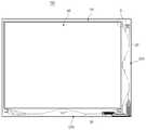
도 1a는 본 발명의 일 실시예에 의한 평판 표시 장치의 평면도이고, 도 1b는 상기 도 1a의 A 영역을 확대한 도면이다.1A is a plan view of a flat panel display according to an exemplary embodiment of the present invention, and FIG. 1B is an enlarged view of region A of FIG. 1A.
도 1a 및 도 1b를 참조하면, 전기 영동 방식으로 구동되는 평판 표시 장 치(display device;100)는 크게 액티브 영역(active region, AR), 주변 영역(peripheral region, PR), 게이트 패드 영역(Gate Pad Region: GPR) 및 데이터 패드 영역(Data Pad Region: DPR)으로 구분된다. 도면에 도시하였지만, 설명하지 않은 GP는 게이트 패드(Gate Pad)이고, DP는 데이터 패드(Data Pad)이다.Referring to FIGS. 1A and 1B, a
상기 액티브 영역(PR)과 주변 영역(PR)을 도 1b를 참조하여 보면, 상기 액티브 영역과 주변 영역에는 복수개의 픽셀 영역이 구획되어 있고, 각 픽셀 영역에는 공통전극, 스토리지 전극 및 화소 전극이 형성되어 있다. 또한, 주변 영역(PR)의 외곽에는 데이터 배선들(DL1,DL2...DLn)과 게이트 배선들(GL1,GL2,...)이 확장 형성되어 있고, 상기 게이트 배선들(GL1, GL2,..GLn)과 데이터 배선들(DL1,...DLn)들 가장자리 영역에는 각각 정전기 방지 회로(ESD)가 형성되어 있다. 상기 정전기 방지 회로들은 모두 정전기 방지 회로 라인(ESD Line)에 공통적으로 연결되어 있다. 또한, 상기 게이트 배선들(GL1, GL2, ..GLn) 사이에는 공통 배선(Vcom1, Vcom2,..Vcomn)들이 확장 형성되어 있고, 이들은 모두 Vcom 공급 라인에 의해 공통적으로 연결되어 있다.Referring to FIG. 1B, the active region PR and the peripheral region PR are divided into a plurality of pixel regions in the active region and the peripheral region, and a common electrode, a storage electrode, and a pixel electrode are formed in each pixel region. It is. In addition, the data lines DL1, DL2... DLn and the gate lines GL1, GL2,... Are extended to the outside of the peripheral area PR. The gate lines GL1, GL2, An antistatic circuit ESD is formed in the edge region of the .... GLn) and the data lines DL1, ... DLn, respectively. The antistatic circuits are all commonly connected to an antistatic circuit line (ESD Line). In addition, common wirings Vcom1, Vcom2, .. Vcomn are formed to be expanded between the gate lines GL1, GL2, .. GLn, and all of them are commonly connected by Vcom supply lines.
상기 액티브 영역은 데이터 배선들(DL1, DL2,..DLn)을 통해서 데이터 신호가 각각의 픽셀 영역으로 공급되어 화상을 디스플레이하는 영역이고, 주변 영역(PR)은 데이터 배선들(DL1, DL2,...DLn)을 통해서 데이터 신호가 일정기간 지속적으로 공급되어 특정 휘도, 예컨대 평판표시장치를 수납 및 보호하는 케이스(도면에는 도시하지 않음.)와 가장 자연스러운 조화를 이룰 수 있는 휘도를 구현한다. 예를 들어, 상기 특정 휘도는 블랙, 화이트 및 회색 휘도 중 어느 하나일 수 있다. 이는, 상기 평판표시장치와 케이스의 조립공정에서 상기 평판표시장치의 주변 영역(PR)이 상기 케이스로부터 노출될 경우, 사용자의 시야에 사용자가 원하는 영상외에 상기 주변 영역이 들어올 수 있기 때문에, 상기 주변 영역(PR)은 상기 케이스와 동일하거나 유사한 특정한 휘도를 구현하여 상기 평판표시장치와 케이스의 조립불량을 개선하기 위함이다. 즉, 상기 주변 영역은 특정한 휘도를 지속적으로 구현함에 따라, 상기 케이스의 조립 불량을 개선할 수 있는 일반적인 액정표시장치의 외곽 블랙매트릭스 역할을 수행할 수 있다.The active area is an area in which a data signal is supplied to each pixel area through data lines DL1, DL2, .. DLn to display an image, and the peripheral area PR is a data line DL1, DL2,. DLn) provides a data signal continuously for a certain period of time to achieve a specific brightness, for example, a brightness that can be most naturally harmonized with a case (not shown in the figure) that houses and protects a flat panel display. For example, the specific luminance may be any one of black, white, and gray luminance. When the peripheral area PR of the flat panel display device is exposed from the case in the assembling process of the flat panel display device and the case, the peripheral area may enter the user's field of view in addition to the image desired by the user. The area PR is intended to improve the assembly failure of the flat panel display and the case by implementing a specific brightness that is the same as or similar to that of the case. In other words, the peripheral region may continuously perform a specific luminance, and thus may serve as an outer black matrix of a general liquid crystal display device that may improve assembly failure of the case.
또한, 도면에 도시된 바와 같이, 액티브 영역에서는 각 픽셀 영역당 개별적으로 화소전극이 형성되어 있지만, 주변 영역에서는 액티브 영역의 둘레를 따라 일체로 더미 화소전극이 형성되어 있다.(도 2 참조)In addition, as shown in the figure, pixel electrodes are individually formed in each pixel region in the active region, but dummy pixel electrodes are integrally formed along the periphery of the active region in the peripheral region (see FIG. 2).
또한, 도 1b에 도시된 바와 같이, 본 발명에서는 데이터 배선들(DL1,DL2,..DLn)과 게이트 배선들(GL1, GL2,..GLn)에는 정전기 방지회로(ESD)를 배치하였지만, 공통 배선들(Vcom1, Vcom2,...Vcomn)에는 정전기 방지회로를 배치하지 않았다. 이것은 정전기 방지회로들을 배치하고, 이들을 공통 공급 라인을 통해 폐루푸(closed loop) 형태로 연결할 경우 공통배선들에 공급되는 전압 레벨(level)이 강하 또는 왜곡되는 문제가 발생하기 때문이다.In addition, as illustrated in FIG. 1B, in the present invention, an antistatic circuit ESD is disposed in the data lines DL1, DL2, .. DLn and the gate lines GL1, GL2, .. GLn, but in common. The antistatic circuit was not disposed on the wirings Vcom1, Vcom2, ... Vcomn. This is because when the antistatic circuits are disposed and connected to each other in a closed loop form through a common supply line, a problem occurs that the voltage level supplied to the common lines drops or is distorted.
따라서, 본 발명에서는 데이터 배선들(DL1,DL2,..DLn) 및 게이트 배선들(GL1, GL2,..GLn)의 각각에는 정전기 방지 회로를 배치하고, 이를 폐루프로 연결한다. 하지만, 공통 배선들(Vcom1, Vcom2,...Vcomn)에는 정전기 방지회로를 배치하지 않고 연결구조도 공통 공급 라인이 오픈된 구조로 형성하였다.Therefore, in the present invention, an antistatic circuit is disposed on each of the data lines DL1, DL2, .. DLn and the gate lines GL1, GL2, .. GLn, and connected to each other by a closed loop. However, the common wirings Vcom1, Vcom2,... Vcomn are formed without a static electricity protection circuit and have a connection structure in which a common supply line is opened.
도 2는 본 발명에 따른 평판 표시 장치의 액티브 영역과 주변 영역의 픽셀 구조를 도시한 평면도이고, 도 3은 도 2의 Ⅰ-Ⅰ'선을 절단한 단면도이다.FIG. 2 is a plan view illustrating pixel structures of an active region and a peripheral region of the flat panel display according to the present invention, and FIG. 3 is a cross-sectional view taken along line II ′ of FIG. 2.
도 2 및 도 3에 도시된 바와 같이, 액티브 영역(AR)에는 다수개의 픽셀 영역이 정의되는데, 각 픽셀 영역은 도 2에 도시된 바와 같이, 게이트 배선(101)과 데이터 배선(103)이 교차 배열되어 단위 픽셀 영역을 정의하고 있다. 또한, 상기 게이트 배선(101)과 데이터 배선(103)의 교차 영역에는 스위칭 소자인 박막 트랜지스터(Thin Film Transistor: TFT)가 배치되어 있고, 픽셀 영역 내에는 제 1 공통전극(108a), 상기 박막 트랜지스터의 드레인 전극(120)으로부터 확장 형성된 스토리지 전극(120a) 및 화소전극(150) 들이 서로 오버랩되도록 배치되어 있다. 상기 제 1 공통전극(108a)은 상기 게이트 배선(101)과 평행하면서 픽셀 영역을 가로질러 배치되는 공통배선(108)으로부터 분기 된다.As shown in FIGS. 2 and 3, a plurality of pixel regions are defined in the active region AR. As illustrated in FIG. 2, the
상기 공통배선(108)은 상기 데이터 배선(103)과 교차되는 영역에서는 그 배선 폭이 좁아지는 구조로 되어 있는데, 이것은 상기 공통배선(108)을 교차하여 지나가는 데이터 배선(103)이 단선되는 것을 방지하기 위함이다. 또한, 상기 데이터 배선(103)과 교차되는 게이트 배선(101) 영역에도 소정의 돌출부가 형성되어 있어 데이터 배선(103)이 상기 게이트 배선(101) 상에 형성될 때 단선되는 것을 방지하도록 하였다. 도 4a에 도시된 바와 같이, 게이트 전극(111)과 대향하는 하측 방향으로 소정의 돌출부가 형성되어 있음을 볼 수 있다.The
특히, 전기 영동 방식으로 구동되는 평판 표시 장치는 하나의 영상 프레임을 장시간 일정하게 유지시켜야하기 때문에 픽셀 영역에서의 스토리지 커패시턴스 값 이 커야한다. 따라서, 제 1 공통전극(108a)과 스토리지 전극(120a)은 픽셀 영역에서의 스토리지 커패시턴스 확보를 위해 확장 형성된 것이다. 즉, 스토리지 전극(120a)과 제 1 공통전극(108a)은 픽셀 영역의 대부분을 차지하도록 넓게 형성되어 있다.In particular, a flat panel display driven by an electrophoretic method needs to maintain a single image frame for a long time, so that a storage capacitance value in a pixel area must be large. Therefore, the first
또한, 전기 영동 방식으로 구동되는 평판 표시 장치는 다른 평판 표시 장치에 비해 구동 전압이 높기 때문에 박막 트랜지스터(TFT)를 크게 형성할 필요가 있다. 즉, 높은 구동 전압에서 동작하기 위해서는 박막 트랜지스터의 채널폭(W)을 넓게 형성하고, 채널 길이(L)는 길게 형성해야 한다(TFT 영역에서의 점선표시). 이에 따라, 전기 영동 방식으로 구동하는 평판 표시 장치에 있어서, 기존 액정표시장치와 같이 박막트랜지스터와 중첩되지 않게 형성될 경우 반사율이 떨어져 화면 품위가 저하될 수 있다. 하지만, 기존 액정표시장치에 있어서, 화소전극이 상기 박막트랜지스터와 중첩되어 형성될 경우, 상기 박막트랜지스터의 채널과 상기 화소전극의 전압에 의해 액정의 이상 구동을 하게 되어 화질에 영향을 미치는 문제점이 있다. 이와 같은 이상 구동 문제는 전기 영동 방식으로 구동되는 평판 표시 장치에도 발생된다.In addition, the flat panel display driven by the electrophoretic method has a higher driving voltage than other flat panel displays, and thus it is necessary to form a thin film transistor TFT. That is, in order to operate at a high driving voltage, the channel width W of the thin film transistor should be wide and the channel length L should be long (dashed line display in the TFT region). Accordingly, in the flat panel display device driven by the electrophoresis method, when the LCD is formed so as not to overlap with the thin film transistor as in the conventional liquid crystal display device, the screen quality may be degraded due to the decrease in reflectance. However, in the conventional liquid crystal display device, when the pixel electrode is formed to overlap the thin film transistor, there is a problem that the abnormal driving of the liquid crystal is caused by the channel of the thin film transistor and the voltage of the pixel electrode, thereby affecting the image quality. . This abnormal driving problem also occurs in a flat panel display driven by an electrophoretic method.
또한, 기존 액정표시장치의 화소 영역에서와 같이 화소 전극이 게이트 배선과 데이터 배선 내측에만 존재하게 되면 전기 영동 방식으로 구동하는 평판 표시 장치에서는 반사율이 떨어져 화면 품위가 저하된다. 이로써, 화소 전극이 데이터 배선과 게이트 배선을 모두 덮도록 형성할 경우, 기생 커패시턴스(Cgs, Cgd)의 크기가 커져서 데이터 신호가 기생 커패시턴스에 의해 크게 왜곡되고, 이것은 킥 백(kick back:ΔV) 전압을 증가시키는 요인으로 작용한다. 이와 같이 킥백 전압의 증가되면 평판 표시 장치의 화질 품위가 저하된다.In addition, when the pixel electrode is present only inside the gate line and the data line, as in the pixel area of the conventional liquid crystal display device, the flatness of the flat panel display device driven by the electrophoresis method reduces the screen quality. As a result, when the pixel electrode is formed to cover both the data wiring and the gate wiring, the parasitic capacitances Cgs and Cgd are increased in size so that the data signal is greatly distorted by the parasitic capacitance, which is a kick back voltage. It acts as a factor to increase. As described above, when the kickback voltage is increased, the image quality of the flat panel display is degraded.
이를 해결하기 위해, 본 발명의 전기 영동 방식 평판 표시 장치에서는 화소 전극을 박막트랜지스터, 게이트 배선과 데이터 배선 중 적어도 어느 하나의 배선상까지 확장하며, 상기 화소전극과 상기 박막트랜지스터, 게이트 배선과 데이터 배선사이에 유전층(141)을 개재하여 화질 품위가 저하되는 것을 최소화하며 이와 동시에 반사율을 향상시킨다.In order to solve this problem, the electrophoretic flat panel display of the present invention extends the pixel electrode to at least one of the thin film transistor, the gate wiring and the data wiring, and the pixel electrode, the thin film transistor, the gate wiring and the data wiring. The quality of the image quality is minimized through the
또한, 본 발명에서와 같이 화소 전극(150)을 확장시킴으로써, 픽셀 영역에서의 반사율을 높이고, 스토리지 커패시턴스의 크기를 크게 하여 하나의 영상 프레임을 장시간 유지할 수 있도록 하였다.In addition, by extending the
또한, 주변 영역의 더미 픽셀 영역에서는 게이트 배선(101)과, 상기 게이트 배선(101)과 교차 배열되는 더미 데이터 배선(123)이 더미 픽셀 영역을 정의한다. 각 더미 픽셀 영역에는 더미 공통전극(108b)과 상기 더미 데이터 배선(123)으로부터 분기되어 상기 더미 공통전극(108b)과 오버랩되는 더미 스토리지 전극(130) 및 상기 더미 스토리지 전극(130)과 전기적으로 연결되면서 주변 영역의 더미 픽셀 영역 전체를 덮도록 형성된 더미 화소전극(160)이 배치되어 있다. 상기 더미 화소전극(160)은 상기 도 1의 주변 영역을 따라 연장되어 하나의 전극 형태로 형성된다.In the dummy pixel area of the peripheral area, the
상기 더미 스토리지 전극(130)은 상기 더미 데이터 배선(123)으로부터 두개의 연결부로부터 인출된 구조로 되어 있지만, 이것은 이에 한정된 것이 아니고 도 6에서와 같이, 하나의 인출부로 연결될 수 있다.The
도 3을 참조하면, 상기 액티브 영역(active region, AR)에서는 데이터 배선(103)을 통하여 영상 신호가 픽셀 영역으로 공급되면, 화소 전극(150)과 잉크필름(170)의 제 2 공통전극(170b) 사이에 전계가 형성된다. 상기 화소 전극(150)과 제 2 공통전극(170b) 사이에 형성되는 전계는 잉크층(170a)의 마이크로 캡슐 내에 포함되어 있는 대전입자들을 이동시켜 블랙 또는 화이트의 화상을 구현한다.Referring to FIG. 3, when the image signal is supplied to the pixel region through the
또한, 상기 주변 영역(peripheral region, PR)에는 더미 데이터 배선(123)을 통하여 화이트, 블랙 또는 회색 중 어느 하나의 색을 구현할 수 있는 영상 신호가 선택적으로 공급되어 더미 화소전극(160)과 잉크필름(170)의 제 2 공통전극(170b) 사이에는 잉크층(170a)에 인가되는 전계가 형성된다. 그러면, 상기 주변 영역은 화이트, 블랙 또는 회색 중 어느 하나의 단일 색이 구현되어, 평판표시장치와 케이스의 조립불량을 개선할 수 있다.In addition, an image signal capable of realizing any color of white, black, or gray is selectively supplied to the peripheral region PR through the
상기 더미 공통전극(108b)은 상기 공통배선(108)으로부터 분기되어 형성된다. 또한, 도면에서는 도시하였지만 설명하지 않은 210a는 화소전극(150)과 스토리지 전극(120a)을 전기적으로 연결하기 위한 제 1 콘택홀이고, 210b는 더미 화소전극(160)과 더미 스토리지 전극(130)을 전기적으로 연결하기 위한 제 2 콘택홀이다.The dummy
도면에는 제 1 및 제 2 콘택홀(210a, 210b)들은 각각 두 개로 형성한 것으로 도시하였으나, 이에 한정되는 것은 아니며 한개 또는 두개 이상으로 형성될 수도 있다.Although the drawings show that the first and
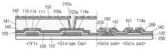
도 2를 참조하여 도 3을 구체적으로 설명하면, 기판(200) 상에는 게이트 배선(101)으로부터 픽셀 영역으로 분기되는 게이트 전극(111)과 공통배선(108)으로부 터 분기되는 제 1 공통전극(108a)이 형성되어 있다. 상기 게이트 전극(111)과 제 1 공통전극(108a)이 형성된 기판(200) 상에는 게이트 절연막(102)이 형성되어 있고, 상기 게이트 전극(111)과 대응되는 게이트 절연막(102) 상에는 박막 트랜지스터(TFT)의 채널층(114)이 형성되어 있다. 상기 채널층(114) 상에는 데이터 배선(103), 상기 데이터 배선(103)으로부터 분기되는 소스 전극(119) 및 상기 소스 전극(119)과 대향하는 드레인 전극(120)이 형성되어 있다. 픽셀 영역에서는 상기 드레인 전극(120)과 일체로 형성되면서 확장 형성된 스토리지 전극(120a)이 상기 제 1 공통전극(108a)과 대응되는 게이트 절연막(102) 상에 형성되어 상기 제 1 공통전극(108a)과 오버랩된다. 상기 제 1 공통전극(108a)의 기능은 상기 스토리지 전극(120a)과의 사이에서 스토리지 커패시턴스를 확보하기 위함이다.Referring to FIG. 2, the
또한, 상기 소스/드레인 전극(119,120)이 형성된 기판(200) 상에는 제 1 보호막(140)이 형성되어 있고, 상기 제 1 보호막(140) 상에는 유전체층(141)과 제 2 보호막(142)이 형성되어 있다. 상기 유전체층(141)은 포토아크릴과 같은 유기막을 사용하는 것이 바람직하나, 경우에 따라서는 무기막 또는 포토레지스트를 사용할 수 있다. 상기 제 2 보호막(142) 상에는 화소전극(150)이 형성되어 있고, 상기 화소전극(150)은 제 1 콘택홀(210a)을 통하여 하부에 형성된 스토리지 전극(120a)과 전기적으로 연결되어 있다. 마찬가지로, 주변 영역의 더미 화소전극(160)도 제 2 콘택홀(210b)을 통하여 더미 스토리지 전극(130)과 전기적으로 연결되어 있다.In addition, a
상기 화소전극(150) 상에는 잉크필름(170)이 부착되어 있는데, 상기 잉크필름(170)은 상기 화소전극(150)과 맞닿는 잉크층(170a), 상기 잉크층(170a)을 보호 하는 보호필름(170c) 및 상기 보호필름(170c)과 잉크층(170a) 사이에 게재된 제 2 공통전극(170b)으로 구성되어 있다. 상기 잉크층(170a)은 서로 다른 종류의 대전입자들을 포함하는 마이크로 캡슐들을 포함하고, 전계에 의해 대전 입자들을 구동시켜 외부 광을 반사하여 화이트 상태 또는 외부 광을 흡수하여 블랙 상태를 구현한다.An
본 발명에서는 화소전극(150)과 제 1 보호막(140) 사이에 유전체층(141) 및 제 2 보호막(142)을 형성하여 화소전극(150) 및 게이트 배선(101)과 데이터 배선(103) 중 적어도 어느 하나의 사이에서 발생 될 수 있는 기생 커패시턴스를 최소화하였다. 즉 유전체층(141)은 상기 화소전극(150)과 스토리지 전극(120a)과의 거리 및 유전율을 조절하여 기생 커패시턴스를 줄이는 역할을 한다.In the present invention, a
또한, 제 1 보호막(140)은 박막 트랜지스터의 전극들과 데이터 배선(103)이 유전체층(141)에 직접적으로 콘택되어 손상되는 것을 방지하고, 제 2 보호막(142)은 화소전극(150)이 유전체층(141)과 직접 콘택되어 손상되는 것을 방지하기 위함이다. 특히, 유전체층(141)이 유기막인 경우에는 유기막으로부터 발생되는 아웃가스로 인해 유전체층(141)과 직접접촉되고 있는 금속 전극이 손상되는데 이를 방지하기 위해 유전체층(141)의 상하층에 보호막을 형성하였다.In addition, the
따라서, 본 발명에서는 액티브 영역에서의 화소전극(150)을 확장 형성하여 반사율을 높여 화질 품위를 개선하였고, 추가적으로 단위 픽셀 영역에서의 스토리지 커패시턴스를 확보하였다.Accordingly, in the present invention, the
평판 표시 장치 제조방법Manufacturing method of flat panel display
도 4a 내지 도 4d는 본 발명의 다른 실시예에 의한 평판 표시 장치 제조방법을 도시한 도면이다.4A to 4D illustrate a method of manufacturing a flat panel display according to another exemplary embodiment of the present invention.
도 3을 참조하면서 도 4a 내지 도 4d의 제조 방법을 설명하면 다음과 같다.The manufacturing method of FIGS. 4A to 4D will be described with reference to FIG. 3.
도 4a에 도시된 바와 같이, 액티브 영역(AR)과 주변 영역(PR)이 구획된 기판(200) 상에 게이트 배선(101), 게이트 전극(111), 공통배선(108), 제 1 공통전극(108a) 및 더미 공통전극(108b)을 형성한다. 상기 게이트 배선(101)과 공통배선(108) 물질은 구리, 크롬, 크롬 합금, 몰리브덴 및 이들의 합금 등을 들 수 있다. 배선 및 전극 형성 방법은 마스크를 포함하는 포토리쏘그라피 방법 및 식각 공정을 이용하여 형성한다. 본 실시 예에서, 공통 배선(108)과 게이트 배선(101)은 액티브 영역뿐만 아니라 주변 영역까지 확장 형성된다.As shown in FIG. 4A, the
또한, 상기 공통배선(108)은 픽셀 영역에서 인접한 픽셀 영역으로 넘어갈 때, 데이터 배선과 교차되는 영역에서 배선 폭이 좁아지도록 형성된다. 이것은 이후 게이트 절연막을 사이에 두고 데이터 배선이 형성될 경우 단차에 의해 데이터 배선이 단선되는 것을 방지하기 위함이다.In addition, the
또한, 상기 게이트 배선(101)에는 상기 게이트 전극(111)과 대향하는 반대 방향에 소정의 돌출부를 형성하여, 이후 데이터 배선이 형성될 때, 단차에 의해 데이터 배선이 단선되는 것을 방지하도록 하였다. 아울러, 상기 게이트 전극(111)은 드레인 전극과 소스 전극이 교차하는 영역에 소정의 홈들을 형성하여, 소스 전극과 드레인 전극 형성시 단차에 의해 전극이 단선되는 것을 방지하도록 하였다.In addition, a predetermined protrusion is formed in the
상기와 같이 게이트 배선(101) 등이 기판(200) 상에 형성되면, 기판(200)의 전 영역 상에 게이트 절연막(102)을 형성한다. 상기 게이트 절연막(102)은 실리콘 산화막(SiOx) 또는 실리콘 질화막(SiNx) 등을 사용할 수 있다.When the
상기와 같이 게이트 배선(101)과 공통배선(108) 등이 기판(200) 상에 형성되면, 도 4b에 도시한 바와 같이, 액티브 영역에서는 게이트 전극(111) 상에 채널층(114)과 소스/드레인 전극(119,120), 스토리지 전극(120a) 및 데이터 배선(103)을 형성한다. 이때, 회절 마스크 또는 하프톤 마스크를 사용하여 상기 채널층(114)과 소스/드레인 전극(119,120) 및 데이터 배선(103)을 동시에 형성한다.When the
이때, 주변 영역에서도 더미 데이터 배선(123)과 상기 더미 데이터 배선(123)으로부터 분기되는 더미 스토리지 전극(130)을 함께 형성한다.In this case, the
또한, 채널층(114)은 아몰퍼스 실리콘막과 인(P)과 같은 도전성 불순물로 고농도 도핑된 n+ 아몰퍼스 실리콘막을 포함할 수 있다. 본 발명에서는 채널층(114:점선표시)의 폭과 길이를 확보하기 위해 상기 소스 전극(119)이 세개의 전극 구조로 형성되어 있고, 이와 대응되는 드레인 전극(120)이 두개의 전극 구조로 형성되어 있다. 따라서, 도 4b에 도시된 바와 같이 소스 전극(119)과 드레인 전극(120)은 전극들이 서로 맞물려진 이중(double)구조로 형성되어 있다. 그리고 이들 전극 사이에는 점선 형태의 채널층(114)이 형성된다. 채널층(114)의 길이와 폭이 종래 박막 트랜지스터의 채널층 보다 훨씬 크게 형성된다.In addition, the
상기와 같이 소스/드레인 전극(119,120) 및 데이터 배선(103)이 기판(200) 상에 형성되면, 도 4c에 도시한 바와 같이, 기판(200)의 전 영역 상에 제 1 보호막(140), 유전체층(141) 및 제 2 보호막(142)을 순차적으로 형성한 다음, 마스크 공정을 적용하여 상기 스토리지 전극(120a) 및 더미 스토리지 전극(130) 상에 제 1 및 제 2 콘택홀(210a, 210b)을 형성한다. 여기서 제 1 보호막(140)과 제 2 보호막(142)은 산화물 또는 질화물과 같은 무기물을 포함할 수 있으며 유기물을 사용할 수도 있다.When the source /
또한, 상기 유전체층(141)은 유기막을 사용하는 것이 바람직하지만, 무기물질 또는 포토레지스트를 사용할 수 있다.In addition, although the organic layer is preferably used as the
상기와 같이 제 1 및 제 2 콘택홀(210a, 210b)이 형성되면, 도 4d에 도시한 바와 같이, 기판(200)의 전 영역에 투명하면서 도전성인 산화 주석 인듐(Indium Tin Oxide, ITO), 산화 아연 인듐(Indium Zinc Oxide, IZO) 및 아몰퍼스 산화 주석 인듐(amorphous Indium Tin Oxide, a-ITO) 중 어느 하나를 형성한다.When the first and
그런 다음, 마스크 공정을 진행하여 액티브 영역의 픽셀 영역에 화소전극(150)을 형성하고, 주변 영역에 더미 화소전극(160)을 형성한다.Then, the mask process is performed to form the
이때, 상기 화소전극(150)은 픽셀 영역을 구획하는 데이터 배선(103)과 게이트 배선(101) 및 박막 트랜지스터(TFT)를 덮을 수 있도록 확장 형성한다.In this case, the
주변 영역에서의 더미 화소전극(160)은 주변 영역 전체 둘레를 따라 일체형 전극 구조로 형성된다. 또한, 도면에서는 도시하지 않았지만, 주변 영역에는 더미 데이터 배선(123)을 통하여 블랙 또는 화이트 데이터 신호만을 공급하여 평판표시장치와 케이스의 조립 불량을 개선하고자 하였다.The
도 5a 내지 도 5d는 본 발명에 따른 평판 표시 장치의 제조 방법을 도시한 도면이다. 제조 공정 영역은 픽셀 영역의 박막 트랜지스터 영역(TFT), 스토리지 커패시턴스 영역(Storage Cap), 게이트 패드(도 1a의 GP) 및 데이터 패드(도 1a의 DP)이다.5A to 5D illustrate a method of manufacturing a flat panel display device according to the present invention. The fabrication process region is a thin film transistor region (TFT), a storage capacitance region (Storage Cap), a gate pad (GP in FIG. 1A) and a data pad (DP in FIG. 1A) in the pixel region.
도 2를 참조하여 도 5a 내지 도 5d의 제조방법을 설명하면, 기판(200) 상에 구리, 크롬, 크롬 합금, 몰리브덴 및 이들의 합금중 어느 하나를 등을 형성한 다음, 마스크를 포함하는 포토리쏘그라피 방법을 사용하여 포토레지스트를 패터닝한다. 패터닝된 포토레지스트를 마스크로 사용하여 습식각 공정을 진행하여 기판(200) 상에 게이트 전극(111), 픽셀 영역 내에 제 1 공통전극(108a), 게이트 배선(101), 공통배선(108) 및 게이트 패드(190)를 형성한다. 상기 게이트 패드(190)는 게이트 배선(101)이 연장되어 도 1의 패드 영역까지 확장되어 형성된다.Referring to FIG. 2, the manufacturing method of FIGS. 5A to 5D will be formed of copper, chromium, chromium alloy, molybdenum, and alloys thereof, etc. on the
상기와 같이 게이트 전극(111)이 기판(200) 상에 형성되면, 도 5b에 도시된 바와 같이, 기판(200)의 전 영역 상에 게이트 절연막(102)을 형성한다. 상기 게이트 절연막(102)은 실리콘 산화막(SiOx) 또는 실리콘 질화막(SiNx) 등을 사용할 수 있다.When the
그런 다음, 계속해서 게이트 절연막(102) 상에 비정질 실리콘층과 도핑된(n+, p+) 비정질 실리콘층 및 금속층을 연속하여 형성한다. 그런 다음, 회절 마스크 또는 하프톤 마스크를 포함하는 포토리쏘그라피 방법을 이용하여 패터닝한 다음, 습식각 및 건식각 공정을 반복적으로 사용하여 박막 트랜지스터의 게이트 전극(111) 상에 채널층(114)과 소스/드레인 전극(119, 120) 및 데이터 배선(103)을 형성한다. 스토리지 커패시턴스 영역에는 상기 드레인 전극(120)과 일체로 형성되면서 픽셀 영역에서 확장 형성된 스토리지 전극(120a)을 형성한다.Then, an amorphous silicon layer, a doped (n +, p +) amorphous silicon layer, and a metal layer are subsequently formed on the
이때, 데이터 패드(data pad) 영역에는 데이터 패드(191)와 상기 데이터 패드(191)와 게이트 절연막(102) 사이에 반도체층(114a)이 존재한다.In this case, a
상기에서와 같이 소스/드레인 전극(119, 120) 및 데이터 배선(103)이 기판(200) 상에 형성되면, 도 5c에 도시된 바와 같이, 기판(200) 상에 제 1 보호막(140)과 유전체층(141) 및 제 2 보호막(142)을 순차적으로 형성한다. 그런 다음, 마스크를 포함하는 포토리쏘그라피 방법을 이용하여 상기 스토리지 전극(120a) 상에 제 1 콘택홀(210a)을 형성한다. 이때, 게이트 패드와 데이터 패드 영역에는 유전체층(141)이 제거되어 제 1 보호막(140)과 제 2 보호막(142)이 게이트 절연막(102) 상에 적층된 구조로 되어 있다. 이때, 제 1 콘택홀 공정에 의해 게이트 패드(190)와 데이터 패드(191)가 노출된다. 즉, 구체적인 공정을 보면 1차적으로 제 1 보호막(140)이 기판(200)의 전 영역 상에 형성되고, 이후 유전체층(141)이 기판(200)의 전 영역 상에 적층된다. 이때, 유전체층(141)에 제 1 콘택홀을 형성하는 공정을 진행하는데, 이때, 패드 영역의 유전체층(141)을 모두 제거한다. 이후, 제 2 보호막(142)을 기판(200) 상에 형성한 다음, 제 1 콘택홀 공정을 진행한다.As described above, when the source /
여기서 제 1 보호막(140)과 제 2 보호막(142)은 산화물 또는 질화물과 같은 무기물을 포함할 수 있으며 유기물을 사용할 수도 있다. 또한, 상기 유전체층(141)은 유기막을 사용하는 것이 바람직하지만, 무기물질 또는 포토레지스트를 사용할 수 있다.The
상기와 같이 제 1 콘택홀(210a)이 형성되면, 도 5d에 도시한 바와 같이, 기판(200)의 전 영역에 투명하면서 도전성인 산화 주석 인듐(Indium Tin Oxide, ITO), 산화 아연 인듐(Indium Zinc Oxide, IZO) 및 아몰퍼스 산화 주석 인듐(amorphous Indium Tin Oxide, a-ITO) 중 어느 하나를 형성한다.When the
그런 다음, 마스크 공정을 진행하여 액티브 영역의 픽셀 영역에 화소전극(150)을 형성하고, 게이트 패드(190) 상에는 게이트 패드전극(250)과 데이터 패드(191) 상에는 데이터 패드전극(260)을 형성한다.Then, a mask process is performed to form the
이때, 상기 화소전극(150)은 픽셀 영역을 구획하는 데이터 배선(103)과 게이트 배선(101) 및 박막 트랜지스터(TFT)를 덮을 수 있도록 확장 형성한다.(도 2 참조)In this case, the
도 2를 참조하면, 주변 영역에서의 더미 화소전극(160)은 주변 영역 전체 둘레를 따라 일체형 전극 구조로 형성된다. 또한, 도면에서는 도시하지 않았지만, 주변 영역에는 더미 데이터 배선(123)을 통하여 블랙 또는 화이트 데이터 신호만을 공급하여 평편표시장치와 케이스의 조립 불량을 개선할 수 있다.Referring to FIG. 2, the
도 6은 본 발명의 또 다른 실시예에 의한 평판 표시 장치의 평면도이다.6 is a plan view of a flat panel display device according to still another embodiment of the present invention.
도 2의 도면부호와 동일한 도면부호는 동일한 구성부를 나타내므로 이를 참조한다.The same reference numerals as the reference numerals of FIG. 2 refer to the same components.
도 6에 도시된 바와 같이, 본 발명의 다른 실시예에 의한 평판 표시 장치의 픽셀 구조의 박막 트랜지스터(TFT)는 두 개의 제 1, 2 게이트 전극(211a, 211b)을 구비한다.As illustrated in FIG. 6, a thin film transistor TFT having a pixel structure of a flat panel display device according to another exemplary embodiment includes two first and
또한, 상기 박막 트랜지스터는 데이터 배선(103)으로부터 분기되는 소스 전극(219)과, 상기 제 1 게이트 전극(211a)과 제 2 게이트 전극(211b) 사이에 배치된 연결전극(218)과, 상기 제 2 게이트 전극(211b)과 일부 오버랩되면서 픽셀 영역의 스토리지 전극(220a)과 연결된 드레인 전극(220)을 구비한다.The thin film transistor may include a
상기 스토리지 전극(220a)은 상기 드레인 전극(220)과 일체로 형성되어 있고, 하부에는 제 1 공통전극(108a)이 배치되고, 상기 스토리지 전극(220a) 상부에는 화소전극(150)이 배치된다. 상기 화소전극(150)은 픽셀 영역을 구획하는 데이터 배선(103)과 게이트 배선(101)을 모두 덮도록 확장 형성된다. 그 기능 및 효과는 도 2에서 설명한 기능 및 효과와 같으므로 이를 참조한다.The
따라서, 상기 게이트 배선(101)을 통하여 구동 신호가 공급되면 상기 박막 트랜지스터의 제 1, 2 게이트 전극(211a,211b)에 구동 전압이 공급되어 턴온 상태가 되고, 이대, 상기 데이터 배선(103)을 통하여 공급되는 데이터 신호는 소오스 전극(219)과 연결전극(218), 드레인 전극(220) 및 스토리지 전극(220a)을 순차적으로 거치면서 상기 화소전극(150)에 데이터 신호를 공급한다.Therefore, when a driving signal is supplied through the
상기와 같이 화소전극(150)에 데이터 신호가 공급되면 도 2와 3에서와 같이 화소전극(150)과 잉크층(170a) 상에 형성된 제 2 공통전극(170b) 사이에 전계가 형성되어 잉크층(170a)의 마이크로 캡슐 내에 포함된 대전입자들을 동작시킨다.When the data signal is supplied to the
상기와 같은 구조의 박막 트랜지스터는 높은 구동전압에 대하여 트랜지스터의 로드를 분산시켜 동작 특성을 향상시킬 수 있다.The thin film transistor having the above structure can improve the operating characteristics by distributing the load of the transistor with respect to a high driving voltage.
도 1a는 본 발명의 일 실시예에 의한 평판 표시 장치의 평면도이다.1A is a plan view of a flat panel display according to an exemplary embodiment of the present invention.
도 1b는 상기 도 1a의 A 영역을 확대한 도면이다.FIG. 1B is an enlarged view of region A of FIG. 1A.
도 2는 본 발명에 따른 평판 표시 장치의 액티브 영역과 주변 영역의 픽셀 구조를 도시한 평면도이다.2 is a plan view illustrating a pixel structure of an active area and a peripheral area of a flat panel display device according to an exemplary embodiment of the present invention.
도 3은 도 2의 Ⅰ-Ⅰ'선을 절단한 단면도이다.3 is a cross-sectional view taken along the line II ′ of FIG. 2.
도 4a 내지 도 4d는 본 발명의 다른 실시예에 의한 평판 표시 장치 제조방법을 도시한 도면이다.4A to 4D illustrate a method of manufacturing a flat panel display according to another exemplary embodiment of the present invention.
도 5a 내지 도 5d는 본 발명에 따른 평판 표시 장치의 제조 방법을 도시한 도면이다.5A to 5D illustrate a method of manufacturing a flat panel display device according to the present invention.
도 6은 본 발명의 또 다른 실시예에 의한 평판 표시 장치의 평면도이다.6 is a plan view of a flat panel display device according to still another embodiment of the present invention.
*도면의 주요 부분에 대한 부호의 설명*Description of the Related Art [0002]
100: 평판 표시 장치101: 게이트 배선100: flat panel display 101: gate wiring
103: 데이터 배선108: 공통배선103: data wiring 108: common wiring
108a: 제 1 공통전극108b: 더미 공통전극108a: first
119: 소스 전극120: 드레인 전극119
150: 화소전극160: 더미 화소전극150: pixel electrode 160: dummy pixel electrode
Claims (15)
Translated fromKoreanPriority Applications (5)
| Application Number | Priority Date | Filing Date | Title |
|---|---|---|---|
| KR1020080014899AKR101346921B1 (en) | 2008-02-19 | 2008-02-19 | A flat display device and method of manufacturing the same |
| TW097131836ATWI413842B (en) | 2008-02-19 | 2008-08-20 | Flat display device and method for manufacturing the same |
| CN2008101764869ACN101515102B (en) | 2008-02-19 | 2008-11-13 | Flat display device and method for manufacturing the same |
| US12/318,519US8148181B2 (en) | 2008-02-19 | 2008-12-30 | Method for manufacturing flat display device |
| US13/406,072US8410484B2 (en) | 2008-02-19 | 2012-02-27 | Flat display device with a dummy pixel integrally formed in a peripheral region |
Applications Claiming Priority (1)
| Application Number | Priority Date | Filing Date | Title |
|---|---|---|---|
| KR1020080014899AKR101346921B1 (en) | 2008-02-19 | 2008-02-19 | A flat display device and method of manufacturing the same |
Publications (2)
| Publication Number | Publication Date |
|---|---|
| KR20090089630A KR20090089630A (en) | 2009-08-24 |
| KR101346921B1true KR101346921B1 (en) | 2014-01-02 |
Family
ID=40954264
Family Applications (1)
| Application Number | Title | Priority Date | Filing Date |
|---|---|---|---|
| KR1020080014899AActiveKR101346921B1 (en) | 2008-02-19 | 2008-02-19 | A flat display device and method of manufacturing the same |
Country Status (4)
| Country | Link |
|---|---|
| US (2) | US8148181B2 (en) |
| KR (1) | KR101346921B1 (en) |
| CN (1) | CN101515102B (en) |
| TW (1) | TWI413842B (en) |
Families Citing this family (40)
| Publication number | Priority date | Publication date | Assignee | Title |
|---|---|---|---|---|
| CN101706637B (en)* | 2009-04-03 | 2011-07-13 | 深超光电(深圳)有限公司 | Pixel electrode structure with high display quality |
| KR101276749B1 (en) | 2009-08-03 | 2013-06-19 | 엘지디스플레이 주식회사 | Electrophoretic display device and manufacturing method thereof |
| KR101263659B1 (en)* | 2009-12-18 | 2013-05-21 | 엘지디스플레이 주식회사 | Electrophoretic Display Apparatus and Method for Manuafacturing The Same |
| KR101662135B1 (en)* | 2010-01-15 | 2016-10-05 | 삼성디스플레이 주식회사 | Electrophoretic display panel, method of manufacturing the same and electrophoretic display apparatus having the same |
| KR101127588B1 (en)* | 2010-03-09 | 2012-03-22 | 삼성모바일디스플레이주식회사 | Liquid Crystal Display Panel and Method of Manufacturing the same |
| JP6126775B2 (en)* | 2010-06-25 | 2017-05-10 | 株式会社半導体エネルギー研究所 | Display device |
| KR20120022411A (en)* | 2010-09-02 | 2012-03-12 | 삼성모바일디스플레이주식회사 | Display device and driving method thereof |
| CN102646594A (en)* | 2011-05-20 | 2012-08-22 | 京东方科技集团股份有限公司 | A kind of channel of ESD circuit and preparation method thereof |
| TWI467673B (en)* | 2011-06-09 | 2015-01-01 | Chunghwa Picture Tubes Ltd | Wiring device and display device |
| CN102645811B (en) | 2011-11-23 | 2014-07-02 | 京东方科技集团股份有限公司 | Electronic-paper active substrate and manufacturing method thereof and electronic-paper display screen |
| KR101881895B1 (en)* | 2011-11-30 | 2018-07-26 | 삼성디스플레이 주식회사 | Thin-film transistor array substrate, organic light emitting display device comprising the same and method for manufacturing of the thin-film transistor array substrate |
| KR101341030B1 (en) | 2012-08-29 | 2013-12-13 | 엘지디스플레이 주식회사 | Organic emitting display device and method for manufacturing the same |
| KR102017204B1 (en) | 2012-11-01 | 2019-09-03 | 삼성디스플레이 주식회사 | Thin film trannsistor array panel and manufacturing method thereof |
| CN103066017A (en)* | 2012-12-28 | 2013-04-24 | 北京京东方光电科技有限公司 | Preparing method of array substrate |
| CN103337479B (en)* | 2013-07-05 | 2016-03-30 | 合肥京东方光电科技有限公司 | The manufacture method of a kind of array base palte, display unit and array base palte |
| CN103761935B (en) | 2014-01-21 | 2016-01-06 | 深圳市华星光电技术有限公司 | Display panel |
| NL2012803B1 (en) | 2014-05-12 | 2016-02-24 | Hj Forever Patents B V | Electrophoretic display. |
| US9874775B2 (en)* | 2014-05-28 | 2018-01-23 | Semiconductor Energy Laboratory Co., Ltd. | Liquid crystal display device and electronic device |
| US9564458B2 (en)* | 2014-11-26 | 2017-02-07 | Shenzhen China Star Optoelectronics Technology Co., Ltd. | TFT substrates and the manufacturing method thereof |
| TWI544272B (en) | 2015-04-17 | 2016-08-01 | 元太科技工業股份有限公司 | Display device |
| KR102484885B1 (en) | 2015-12-07 | 2023-01-05 | 엘지디스플레이 주식회사 | Display device integrated with touch screen panel and method for fabricating the same |
| KR102542186B1 (en)* | 2016-04-04 | 2023-06-13 | 삼성디스플레이 주식회사 | Display device |
| KR101951939B1 (en)* | 2016-08-26 | 2019-02-25 | 엘지디스플레이 주식회사 | Display Device |
| KR102538750B1 (en) | 2016-11-29 | 2023-06-02 | 엘지디스플레이 주식회사 | Liquid crystal display device |
| CN107357105A (en)* | 2017-09-05 | 2017-11-17 | 京东方科技集团股份有限公司 | A kind of array base palte, display panel, display device |
| CN107610663B (en)* | 2017-09-25 | 2019-12-03 | 武汉华星光电技术有限公司 | The virtual circuit and driving circuit of panel display apparatus |
| CN109830181A (en) | 2017-11-23 | 2019-05-31 | 群创光电股份有限公司 | Display device |
| CN207424484U (en)* | 2017-11-27 | 2018-05-29 | 京东方科技集团股份有限公司 | A kind of array substrate and display device |
| KR102446077B1 (en)* | 2017-12-29 | 2022-09-21 | 엘지디스플레이 주식회사 | Electroluminescent Display Device |
| CN108550582B (en)* | 2018-05-09 | 2022-11-08 | 京东方科技集团股份有限公司 | Display substrate, method for manufacturing the same, and display device |
| CN108803173B (en)* | 2018-07-02 | 2021-08-10 | 京东方科技集团股份有限公司 | Array substrate, manufacturing method thereof and display device |
| CN110286527B (en)* | 2019-06-25 | 2022-04-15 | 京东方科技集团股份有限公司 | Dye liquid crystal dimming panel, manufacturing method thereof and double-layer dye liquid crystal dimming panel |
| CN110571228B (en)* | 2019-09-26 | 2022-02-01 | 京东方科技集团股份有限公司 | Array substrate, liquid crystal display panel and display device |
| CN110596987B (en)* | 2019-09-30 | 2023-09-08 | 京东方科技集团股份有限公司 | Display substrate and display device |
| CN110675804B (en)* | 2019-11-15 | 2022-09-13 | 福州京东方光电科技有限公司 | Shutdown discharge circuit, control method thereof, display panel and display device |
| CN113311623B (en)* | 2020-02-27 | 2023-11-21 | 夏普株式会社 | display panel |
| CN111427206B (en)* | 2020-03-24 | 2022-07-26 | 京东方科技集团股份有限公司 | Array substrate and display device |
| CN111584757B (en)* | 2020-05-27 | 2022-12-06 | 京东方科技集团股份有限公司 | Display mother board and manufacturing method of display substrate |
| US11856796B2 (en)* | 2021-07-16 | 2023-12-26 | Taiwan Semiconductor Manufacturing Company, Ltd. | Semiconductor memory devices and methods of manufacturing thereof |
| TWI793921B (en) | 2021-12-13 | 2023-02-21 | 友達光電股份有限公司 | Display panel |
Citations (2)
| Publication number | Priority date | Publication date | Assignee | Title |
|---|---|---|---|---|
| US7138655B2 (en) | 2002-11-20 | 2006-11-21 | Samsung Electronics Co., Ltd. | Thin film transistor array panel including symmetrically aligned thin film transistors and manufacturing method thereof |
| US7687806B2 (en) | 2006-03-23 | 2010-03-30 | Prime View International Co., Ltd. | E-ink display and method for repairing the same |
Family Cites Families (10)
| Publication number | Priority date | Publication date | Assignee | Title |
|---|---|---|---|---|
| KR100715943B1 (en)* | 2001-01-29 | 2007-05-08 | 삼성전자주식회사 | LCD and its manufacturing method |
| TWI291072B (en)* | 2001-09-28 | 2007-12-11 | Sanyo Electric Co | Liquid crystal display unit |
| KR100858297B1 (en)* | 2001-11-02 | 2008-09-11 | 삼성전자주식회사 | Reflective-transmissive type liquid crystal display device and method of manufacturing the same |
| JP4197233B2 (en)* | 2002-03-20 | 2008-12-17 | 株式会社日立製作所 | Display device |
| KR100956338B1 (en)* | 2002-12-11 | 2010-05-06 | 삼성전자주식회사 | Thin Film Transistor Array Substrates for Thin-Ray Detectors |
| KR100745415B1 (en)* | 2002-12-27 | 2007-08-03 | 엘지.필립스 엘시디 주식회사 | Data pad portion of liquid crystal display panel and manufacturing method thereof |
| JP4239873B2 (en)* | 2003-05-19 | 2009-03-18 | セイコーエプソン株式会社 | Electro-optical device and electronic apparatus |
| JP4285158B2 (en)* | 2003-08-29 | 2009-06-24 | セイコーエプソン株式会社 | Electro-optical device and electronic apparatus |
| KR101202983B1 (en)* | 2005-09-13 | 2012-11-20 | 엘지디스플레이 주식회사 | An array substrate for trans-flective liquid crystal display device and fabrication method of the same |
| JP2008026348A (en)* | 2006-07-18 | 2008-02-07 | Seiko Epson Corp | Electro-optical device and electronic apparatus |
- 2008
- 2008-02-19KRKR1020080014899Apatent/KR101346921B1/enactiveActive
- 2008-08-20TWTW097131836Apatent/TWI413842B/ennot_activeIP Right Cessation
- 2008-11-13CNCN2008101764869Apatent/CN101515102B/ennot_activeExpired - Fee Related
- 2008-12-30USUS12/318,519patent/US8148181B2/enactiveActive
- 2012
- 2012-02-27USUS13/406,072patent/US8410484B2/enactiveActive
Patent Citations (2)
| Publication number | Priority date | Publication date | Assignee | Title |
|---|---|---|---|---|
| US7138655B2 (en) | 2002-11-20 | 2006-11-21 | Samsung Electronics Co., Ltd. | Thin film transistor array panel including symmetrically aligned thin film transistors and manufacturing method thereof |
| US7687806B2 (en) | 2006-03-23 | 2010-03-30 | Prime View International Co., Ltd. | E-ink display and method for repairing the same |
Also Published As
| Publication number | Publication date |
|---|---|
| US8410484B2 (en) | 2013-04-02 |
| US20120153290A1 (en) | 2012-06-21 |
| CN101515102A (en) | 2009-08-26 |
| US20090206339A1 (en) | 2009-08-20 |
| CN101515102B (en) | 2011-01-05 |
| TW200937089A (en) | 2009-09-01 |
| TWI413842B (en) | 2013-11-01 |
| US8148181B2 (en) | 2012-04-03 |
| KR20090089630A (en) | 2009-08-24 |
Similar Documents
| Publication | Publication Date | Title |
|---|---|---|
| KR101346921B1 (en) | A flat display device and method of manufacturing the same | |
| JP4277874B2 (en) | Manufacturing method of electro-optical device | |
| US9240149B2 (en) | Liquid crystal display device and method of fabricating the same | |
| KR100602062B1 (en) | Horizontal field applied liquid crystal display device and manufacturing method thereof | |
| US10444579B2 (en) | Display substrate and manufacturing method thereof, and display device | |
| KR100470208B1 (en) | Liquid crystal display apparatus of horizontal electronic field applying type and fabricating method thereof | |
| JP2008070873A (en) | Flat panel display | |
| JP2008203761A (en) | Display device | |
| JP5940163B2 (en) | Semiconductor device and display device | |
| KR20100049385A (en) | Array substrate of organic electro-luminescent device | |
| KR100838185B1 (en) | Array substrate, liquid crystal display device using same, and manufacturing method thereof | |
| KR20030094452A (en) | Thin film transistor array panel for liquid crystal display | |
| KR20160082738A (en) | Organic lighting emitting display device | |
| KR101784445B1 (en) | Array substrate for Liquid crystal display device | |
| US8456582B2 (en) | Active device, pixel structure and display panel | |
| US8786815B2 (en) | Driving circuit and display panel having the same | |
| KR100558718B1 (en) | LCD panel and manufacturing method thereof | |
| US11740524B2 (en) | Liquid crystal display device | |
| KR100646172B1 (en) | LCD and its manufacturing method | |
| KR100583313B1 (en) | LCD and its manufacturing method | |
| US12164204B2 (en) | Display device | |
| KR101222537B1 (en) | Liquid Crystal Display Pane And Method for Fabricating Thereof | |
| KR102141561B1 (en) | Liquid crystal display device and method of manufacturing the same | |
| KR102113603B1 (en) | Thin film transistor array substrate and method of fabricating the same | |
| CN118201413A (en) | Display device and method for manufacturing the same |
Legal Events
| Date | Code | Title | Description |
|---|---|---|---|
| PA0109 | Patent application | Patent event code:PA01091R01D Comment text:Patent Application Patent event date:20080219 | |
| PG1501 | Laying open of application | ||
| A201 | Request for examination | ||
| PA0201 | Request for examination | Patent event code:PA02012R01D Patent event date:20111103 Comment text:Request for Examination of Application Patent event code:PA02011R01I Patent event date:20080219 Comment text:Patent Application | |
| E902 | Notification of reason for refusal | ||
| PE0902 | Notice of grounds for rejection | Comment text:Notification of reason for refusal Patent event date:20121211 Patent event code:PE09021S01D | |
| E902 | Notification of reason for refusal | ||
| PE0902 | Notice of grounds for rejection | Comment text:Notification of reason for refusal Patent event date:20130502 Patent event code:PE09021S01D | |
| E701 | Decision to grant or registration of patent right | ||
| PE0701 | Decision of registration | Patent event code:PE07011S01D Comment text:Decision to Grant Registration Patent event date:20131002 | |
| GRNT | Written decision to grant | ||
| PR0701 | Registration of establishment | Comment text:Registration of Establishment Patent event date:20131224 Patent event code:PR07011E01D | |
| PR1002 | Payment of registration fee | Payment date:20131224 End annual number:3 Start annual number:1 | |
| PG1601 | Publication of registration | ||
| FPAY | Annual fee payment | Payment date:20161118 Year of fee payment:4 | |
| PR1001 | Payment of annual fee | Payment date:20161118 Start annual number:4 End annual number:4 | |
| FPAY | Annual fee payment | Payment date:20171116 Year of fee payment:5 | |
| PR1001 | Payment of annual fee | Payment date:20171116 Start annual number:5 End annual number:5 | |
| FPAY | Annual fee payment | Payment date:20181114 Year of fee payment:6 | |
| PR1001 | Payment of annual fee | Payment date:20181114 Start annual number:6 End annual number:6 | |
| FPAY | Annual fee payment | Payment date:20191113 Year of fee payment:7 | |
| PR1001 | Payment of annual fee | Payment date:20191113 Start annual number:7 End annual number:7 | |
| PR1001 | Payment of annual fee | Payment date:20211116 Start annual number:9 End annual number:9 | |
| PR1001 | Payment of annual fee | Payment date:20221115 Start annual number:10 End annual number:10 | |
| PR1001 | Payment of annual fee | Payment date:20231128 Start annual number:11 End annual number:11 |