KR101344441B1 - Image sensor and fabricating method thereof - Google Patents
Image sensor and fabricating method thereofDownload PDFInfo
- Publication number
- KR101344441B1 KR101344441B1KR1020070071330AKR20070071330AKR101344441B1KR 101344441 B1KR101344441 B1KR 101344441B1KR 1020070071330 AKR1020070071330 AKR 1020070071330AKR 20070071330 AKR20070071330 AKR 20070071330AKR 101344441 B1KR101344441 B1KR 101344441B1
- Authority
- KR
- South Korea
- Prior art keywords
- voltage
- transistor
- conductivity type
- source follower
- gate
- Prior art date
- Legal status (The legal status is an assumption and is not a legal conclusion. Google has not performed a legal analysis and makes no representation as to the accuracy of the status listed.)
- Active
Links
Images


Classifications
- H—ELECTRICITY
- H10—SEMICONDUCTOR DEVICES; ELECTRIC SOLID-STATE DEVICES NOT OTHERWISE PROVIDED FOR
- H10F—INORGANIC SEMICONDUCTOR DEVICES SENSITIVE TO INFRARED RADIATION, LIGHT, ELECTROMAGNETIC RADIATION OF SHORTER WAVELENGTH OR CORPUSCULAR RADIATION
- H10F39/00—Integrated devices, or assemblies of multiple devices, comprising at least one element covered by group H10F30/00, e.g. radiation detectors comprising photodiode arrays
- H10F39/10—Integrated devices
- H10F39/12—Image sensors
- H—ELECTRICITY
- H04—ELECTRIC COMMUNICATION TECHNIQUE
- H04N—PICTORIAL COMMUNICATION, e.g. TELEVISION
- H04N25/00—Circuitry of solid-state image sensors [SSIS]; Control thereof
- H04N25/60—Noise processing, e.g. detecting, correcting, reducing or removing noise
- H04N25/616—Noise processing, e.g. detecting, correcting, reducing or removing noise involving a correlated sampling function, e.g. correlated double sampling [CDS] or triple sampling
- H—ELECTRICITY
- H04—ELECTRIC COMMUNICATION TECHNIQUE
- H04N—PICTORIAL COMMUNICATION, e.g. TELEVISION
- H04N25/00—Circuitry of solid-state image sensors [SSIS]; Control thereof
- H04N25/70—SSIS architectures; Circuits associated therewith
- H04N25/76—Addressed sensors, e.g. MOS or CMOS sensors
- H—ELECTRICITY
- H10—SEMICONDUCTOR DEVICES; ELECTRIC SOLID-STATE DEVICES NOT OTHERWISE PROVIDED FOR
- H10F—INORGANIC SEMICONDUCTOR DEVICES SENSITIVE TO INFRARED RADIATION, LIGHT, ELECTROMAGNETIC RADIATION OF SHORTER WAVELENGTH OR CORPUSCULAR RADIATION
- H10F39/00—Integrated devices, or assemblies of multiple devices, comprising at least one element covered by group H10F30/00, e.g. radiation detectors comprising photodiode arrays
- H10F39/011—Manufacture or treatment of image sensors covered by group H10F39/12
- H10F39/014—Manufacture or treatment of image sensors covered by group H10F39/12 of CMOS image sensors
- H—ELECTRICITY
- H10—SEMICONDUCTOR DEVICES; ELECTRIC SOLID-STATE DEVICES NOT OTHERWISE PROVIDED FOR
- H10F—INORGANIC SEMICONDUCTOR DEVICES SENSITIVE TO INFRARED RADIATION, LIGHT, ELECTROMAGNETIC RADIATION OF SHORTER WAVELENGTH OR CORPUSCULAR RADIATION
- H10F39/00—Integrated devices, or assemblies of multiple devices, comprising at least one element covered by group H10F30/00, e.g. radiation detectors comprising photodiode arrays
- H10F39/80—Constructional details of image sensors
- H10F39/803—Pixels having integrated switching, control, storage or amplification elements
Landscapes
- Engineering & Computer Science (AREA)
- Multimedia (AREA)
- Signal Processing (AREA)
- Transforming Light Signals Into Electric Signals (AREA)
- Solid State Image Pick-Up Elements (AREA)
Abstract
Translated fromKoreanDescription
Translated fromKorean본 발명은 이미지 센서 및 그 제조 방법에 관한 것으로, 보다 자세하게는 MOS 이미지 센서 및 그 제조 방법에 관한 것이다.The present invention relates to an image sensor and a method of manufacturing the same, and more particularly, to a MOS image sensor and a method of manufacturing the same.
이미지 센서(image sensor)는 광학 영상을 전기 신호로 변환시킨다. 최근 들어, 컴퓨터 산업과 통신 산업의 발달에 따라 디지털 카메라, 캠코더, PCS(Personal Communication System), 게임 기기, 경비용 카메라, 의료용 마이크로 카메라, 로보트 등 다양한 분야에서 성능이 향상된 이미지 센서의 수요가 증대되고 있다.An image sensor converts an optical image into an electrical signal. Recently, with the development of the computer industry and the communication industry, the demand for improved image sensors in various fields such as digital cameras, camcorders, personal communication systems (PCS), gaming devices, security cameras, medical micro cameras, robots, etc. is increasing. have.
MOS 이미지 센서는 구동 방식이 간편하고 다양한 스캐닝(scanning) 방식으로 구현 가능하다. 또한, 신호 처리 회로를 단일칩에 집적할 수 있어 제품의 소형화가 가능하며, MOS 공정 기술을 호환하여 사용할 수 있어 제조 단가를 낮출 수 있다. 전력 소모 또한 매우 낮아 배터리 용량이 제한적인 제품에 적용이 용이하다. 따라서, MOS 이미지 센서는 기술 개발과 함께 고해상도가 구현 가능함에 따라 그 사용이 급격히 늘어나고 있다.The MOS image sensor is simple to drive and can be implemented by various scanning methods. In addition, since the signal processing circuit can be integrated on a single chip, the product can be miniaturized, and the MOS process technology can be used interchangeably to reduce the manufacturing cost. Power consumption is also very low, making it easy to apply to products with limited battery capacity. Therefore, the use of MOS image sensors is rapidly increasing as high resolution can be implemented along with technology development.
이러한 MOS 이미지 센서에서 사용되는 단위 픽셀은, 입사광에 응답하여 전하 를 생성하고 검출 노드의 전압을 변화시키는 광전 변환 소자와, 상기 검출 노드와 커플링되고 소오스 팔로워 동작을 하는 소오스 팔로워 트랜지스터(source follower transistor) 등을 포함한다.The unit pixel used in such a MOS image sensor includes a photoelectric conversion element that generates charge in response to incident light and changes a voltage of a detection node, and a source follower transistor coupled to the detection node and having a source follower operation. ), And the like.
본 발명이 해결하고자 하는 과제는, 선형성 특성(linearity characteristics)이 개선된 소오스 팔로워 트랜지스터를 포함하는 이미지 센서를 제공하는 것이다.An object of the present invention is to provide an image sensor including a source follower transistor having improved linearity characteristics.
본 발명이 해결하고자 하는 다른 과제는, 상기 이미지 센서의 제조 방법을 제공하는 것이다.Another object of the present invention is to provide a method of manufacturing the image sensor.
본 발명이 해결하고자 하는 과제들은 이상에서 언급한 과제들로 제한되지 않으며, 언급되지 않은 또 다른 과제들은 아래의 기재로부터 당업자에게 명확하게 이해될 수 있을 것이다.Problems to be solved by the present invention are not limited to the above-mentioned problems, and other problems not mentioned will be clearly understood by those skilled in the art from the following description.
상기 기술적 과제를 달성하기 위한 본 발명의 비휘발성 메모리 장치의 일 태양은 입사광에 응답하여 전하를 생성하여, 검출 노드의 전압을 변화시키는 광전 변환 소자, 검출 노드와 커플링되고, 제1 일함수를 갖는 물질로 이루어진 게이트를 포함하는 소오스 팔로워 트랜지스터, 및 소오스 팔로워 트랜지스터와 전압 노드 사이에 커플링되고, 제1 일함수보다 낮은 제2 일함수를 갖는 물질로 이루어진 게이트를 포함하는 선택 트랜지스터를 포함한다.One aspect of the nonvolatile memory device of the present invention for achieving the above technical problem is coupled to the photoelectric conversion element, the detection node to generate a charge in response to the incident light, to change the voltage of the detection node, the first work function A source follower transistor comprising a gate of a material having a material, and a selection transistor comprising a gate made of a material having a second work function that is coupled between the source follower transistor and a voltage node and lower than the first work function.
상기 기술적 과제를 달성하기 위한 본 발명의 비휘발성 메모리 장치의 다른 태양은 입사광에 응답하여 전하를 생성하여, 검출 노드의 전압을 변화시키는 광전 변환 소자, 및 검출 노드와 커플링되고 제1 도전형의 도펀트가 도핑된 게이트와, 제1 도전형과 다른 제2 도전형의 도펀트가 도핑된 소오스/드레인과, 제1 도전형의 도펀트가 도핑된 채널을 포함하는 소오스 팔로워 트랜지스터를 포함한다.Another aspect of the nonvolatile memory device of the present invention for achieving the above technical problem is a photoelectric conversion element for generating charge in response to incident light to change the voltage of the detection node, and coupled with the detection node and of the first conductivity type. A source follower transistor includes a dopant-doped gate, a source / drain doped with a dopant of a second conductivity type different from the first conductivity type, and a channel doped with a dopant of a first conductivity type.
상기 기술적 과제를 달성하기 위한 본 발명의 비휘발성 메모리 장치의 또 다른 태양은 입사광에 응답하여 전하를 생성하여, 검출 노드의 전압을 변화시키는 광전 변환 소자, 검출 노드와 커플링되고 제1 문턱 전압을 갖는 소오스 팔로워 트랜지스터, 및 소오스 팔로워 트랜지스터와 전압 노드 사이에 커플링되고, 제1 문턱 전압보다 작은 제2 문턱 전압을 갖는 선택 트랜지스터를 포함한다.Another aspect of the nonvolatile memory device of the present invention for achieving the above technical problem is a photoelectric conversion element for generating a charge in response to incident light to change the voltage of the detection node, coupled with the detection node and the first threshold voltage And a select transistor having a second follower voltage coupled between the source follower transistor and the voltage node, the second follower voltage being less than the first threshold voltage.
상기 기술적 과제를 달성하기 위한 본 발명의 비휘발성 메모리 장치의 또 다른 태양은 입사광에 응답하여 전하를 생성하여, 검출 노드의 전압을 변화시키는 광전 변환 소자, 및 검출 노드와 커플링되고 P형의 도펀트가 도핑된 게이트와, N형의 도펀트가 도핑된 소오스/드레인과, P형의 도펀트가 도핑된 채널을 포함하는 소오스 팔로워 트랜지스터, 전원 전압보다 높은 레벨을 갖는 승압 전압과 커플링된 전압 노드, 및 소오스 팔로워 트랜지스터와 전압 노드 사이에 커플링되고, 승압 전압보다 낮은 레벨의 선택 신호에 응답하여 동작하는 선택 트랜지스터를 포함한다.Another aspect of the nonvolatile memory device of the present invention for achieving the above technical problem is a photoelectric conversion element for generating a charge in response to incident light to change the voltage of the detection node, and a P-type dopant coupled with the detection node A source follower transistor comprising a doped gate, a source / drain doped with an N-type dopant, a channel doped with a P-type dopant, a voltage node coupled with a boosted voltage having a level higher than the supply voltage, and And a select transistor coupled between the source follower transistor and the voltage node, the select transistor operative in response to a select signal at a level lower than the boosted voltage.
상기 다른 기술적 과제를 달성하기 위한 본 발명의 비휘발성 메모리 장치의 구동 방법의 일 태양은 센싱 어레이 영역과 주변 회로 영역이 정의된 기판을 제공하고, 기판의 센싱 어레이 영역 내에 제1 도전형의 불순물을 이온 주입하여 채널을 형성하고, 기판의 센싱 어레이 영역 상에 제1 게이트를 형성하고, 제1 게이트의 양측의 기판 내에 제2 도전형의 불순물을 이온 주입하여 소오스/드레인을 형성하고, 제1 게이트에 제1 도전형의 불순물을 이온 주입하여 소오스 팔로워 트랜지스터를 완성한다.An aspect of the present invention provides a substrate in which a sensing array region and a peripheral circuit region are defined, and provides a first conductivity type impurity in the sensing array region of the substrate. A channel is formed by ion implantation, a first gate is formed on a sensing array region of the substrate, and a source / drain is formed by ion implanting impurities of a second conductivity type into the substrate on both sides of the first gate, and the first gate is formed. The source follower transistor is completed by ion implanting impurities of the first conductivity type into the source follower transistor.
본 발명의 기타 구체적인 사항들은 상세한 설명 및 도면들에 포함되어 있다.Other specific details of the invention are included in the detailed description and drawings.
상기한 바와 같은 이미지 센서 및 그 제조 방법에 따르면, 소오스 팔로워 트랜지스터가 포화 영역에서 안정적으로 동작할 수 있다. 따라서, 소오스 팔로워 트랜지스터의 선형성 특성이 개선될 수 있다.According to the image sensor as described above and a method of manufacturing the same, the source follower transistor can operate stably in the saturation region. Thus, the linearity characteristic of the source follower transistor can be improved.
본 발명의 이점 및 특징, 그리고 그것들을 달성하는 방법은 첨부되는 도면과 함께 상세하게 후술되어 있는 실시예들을 참조하면 명확해질 것이다. 그러나 본 발명은 이하에서 개시되는 실시예들에 한정되는 것이 아니라 서로 다른 다양한 형태로 구현될 것이며, 단지 본 실시예들은 본 발명의 개시가 완전하도록 하며, 본 발명이 속하는 기술분야에서 통상의 지식을 가진 자에게 발명의 범주를 완전하게 알려주기 위해 제공되는 것이며, 본 발명은 청구항의 범주에 의해 정의될 뿐이다. 명세서 전체에 걸쳐 동일 참조 부호는 동일 구성 요소를 지칭한다.Advantages and features of the present invention and methods for achieving them will be apparent with reference to the embodiments described below in detail with the accompanying drawings. The present invention may, however, be embodied in many different forms and should not be construed as being limited to the embodiments set forth herein. Rather, these embodiments are provided so that this disclosure will be thorough and complete, and will fully convey the scope of the invention to those skilled in the art. Is provided to fully convey the scope of the invention to those skilled in the art, and the invention is only defined by the scope of the claims. Like reference numerals refer to like elements throughout.
하나의 소자(elements)가 다른 소자와 "접속된(connected to)" 또는 "커플링된(coupled to)" 이라고 지칭되는 것은, 다른 소자와 직접 연결 또는 커플링된 경우 또는 중간에 다른 소자를 개재한 경우를 모두 포함한다. 반면, 하나의 소자가 다른 소자와 "직접 접속된(directly connected to)" 또는 "직접 커플링된(directly coupled to)"으로 지칭되는 것은 중간에 다른 소자를 개재하지 않은 것을 나타낸다. 명세서 전체에 걸쳐 동일 참조 부호는 동일 구성 요소를 지칭한다. "및/또는" 은 언급된 아이템들의 각각 및 하나 이상의 모든 조합을 포함한다.When an element is referred to as being "connected to" or "coupled to" with another element, it may be directly connected to or coupled with another element or through another element in between. This includes all cases. On the other hand, when one element is referred to as being "directly connected to" or "directly coupled to " another element, it does not intervene another element in the middle. Like reference numerals refer to like elements throughout. "And / or" include each and every combination of one or more of the mentioned items.
비록 제1, 제2 등이 다양한 소자, 구성요소 및/또는 섹션들을 서술하기 위해서 사용되나, 이들 소자, 구성요소 및/또는 섹션들은 이들 용어에 의해 제한되지 않음은 물론이다. 이들 용어들은 단지 하나의 소자, 구성요소 또는 섹션들을 다른 소자, 구성요소 또는 섹션들과 구별하기 위하여 사용하는 것이다. 따라서, 이하에서 언급되는 제1 소자, 제1 구성요소 또는 제1 섹션은 본 발명의 기술적 사상 내에서 제2 소자, 제2 구성요소 또는 제2 섹션일 수도 있음은 물론이다.Although the first, second, etc. are used to describe various elements, components and / or sections, it is needless to say that these elements, components and / or sections are not limited by these terms. These terms are only used to distinguish one element, element or section from another element, element or section. Therefore, it goes without saying that the first element, the first element or the first section mentioned below may be the second element, the second element or the second section within the technical spirit of the present invention.
본 명세서에서 사용된 용어는 실시예들을 설명하기 위한 것이며 본 발명을 제한하고자 하는 것은 아니다. 본 명세서에서, 단수형은 문구에서 특별히 언급하지 않는 한 복수형도 포함한다. 명세서에서 사용되는 "포함한다(comprises)" 및/또는 "이루어지다(made of)"는 언급된 구성요소, 단계, 동작 및/또는 소자는 하나 이상의 다른 구성요소, 단계, 동작 및/또는 소자의 존재 또는 추가를 배제하지 않는다.The terminology used herein is for the purpose of describing particular embodiments only and is not intended to be limiting of the invention. In the present specification, the singular form includes plural forms unless otherwise specified in the specification. As used herein, the terms "comprises" and / or "made of" means that a component, step, operation, and / or element may be embodied in one or more other components, steps, operations, and / And does not exclude the presence or addition thereof.
다른 정의가 없다면, 본 명세서에서 사용되는 모든 용어(기술 및 과학적 용어를 포함)는 본 발명이 속하는 기술분야에서 통상의 지식을 가진 자에게 공통적으로 이해될 수 있는 의미로 사용될 수 있을 것이다. 또 일반적으로 사용되는 사전에 정의되어 있는 용어들은 명백하게 특별히 정의되어 있지 않는 한 이상적으로 또는 과도하게 해석되지 않는다.Unless otherwise defined, all terms (including technical and scientific terms) used in the present specification may be used in a sense that can be commonly understood by those skilled in the art. Also, commonly used predefined terms are not ideally or excessively interpreted unless explicitly defined otherwise.
이하 본 발명의 실시예들에서는 이미지 센서의 일 예로 CMOS 이미지 센서를 예시할 것이다. 그러나, 본 발명에 따른 이미지 센서는 NMOS 또는 PMOS 공정만을 적용하거나 NMOS와 PMOS 공정을 모두 사용하는 CMOS 공정을 적용하여 형성한 이미 지 센서를 모두 포함할 수 있다.Hereinafter, embodiments of the present invention will exemplify a CMOS image sensor as an example of an image sensor. However, the image sensor according to the present invention may include both an image sensor formed by applying only a NMOS or PMOS process or a CMOS process using both NMOS and PMOS processes.
도 1은 본 발명의 실시예들에 따른 이미지 센서의 블록도이다.1 is a block diagram of an image sensor according to example embodiments.
도 1을 참고하면, 본 발명의 실시예들에 따른 이미지 센서는 광전 변환 소자를 포함하는 픽셀들이 이차원적으로 배열되어 이루어진 액티브 픽셀 센서(APS) 어레이(10), 타이밍 발생기(timing generator)(20), 행 디코더(row decoder)(30), 행 드라이버(row driver)(40), 상관 이중 샘플러(Correlated Double Sampler, CDS)(50), 아날로그 디지털 컨버터(Analog to Digital Converter, ADC)(60), 래치부(latch)(70), 열 디코더(column decoder)(80) 등을 포함한다.1, an image sensor according to embodiments of the present invention includes an active pixel sensor (APS)
APS 어레이(10)는 2차원적으로 배열된 다수의 단위 픽셀들을 포함한다. 다수의 단위 픽셀들은 광학 영상을 전기적인 출력 신호로 변환하는 역할을 한다. APS 어레이(10)는 행 드라이버(40)로부터 선택 신호(SEL), 리셋 신호(RX), 전하 전송 신호(TX) 등 다수의 구동 신호를 수신하여 구동된다. 또한, 변환된 전기적인 출력 신호는 수직 신호 라인를 통해서 상관 이중 샘플러(50)에 제공된다.The
타이밍 발생기(20)는 행 디코더(30) 및 열 디코더(80)에 타이밍(timing) 신호 및 제어 신호를 제공한다.The
행 드라이버(40)는 행 디코더(30)에서 디코딩된 결과에 따라 다수의 단위 픽셀들을 구동하기 위한 다수의 구동 신호를 액티브 픽셀 센서 어레이(10)에 제공한다. 일반적으로 행렬 형태로 단위 픽셀이 배열된 경우에는 각 행별로 구동 신호를 제공한다.The
상관 이중 샘플러(50)는 액티브 픽셀 센서 어레이(10)에 형성된 출력 신호를 수직 신호 라인을 통해 수신하여 유지(hold) 및 샘플링한다. 즉, 특정한 잡음 레벨(noise level)과, 상기 출력 신호에 의한 신호 레벨을 이중으로 샘플링하여, 잡음 레벨과 신호 레벨의 차이에 해당하는 차이 레벨을 출력한다.The correlated
아날로그 디지털 컨버터(60)는 차이 레벨에 해당하는 아날로그 신호를 디지털 신호로 변환하여 출력한다.The analog-to-
래치부(70)는 디지털 신호를 래치(latch)하고, 래치된 신호는 컬럼 디코더(80)에서 디코딩 결과에 따라 순차적으로 영상 신호 처리부(도면 미도시)로 출력된다.The
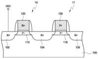
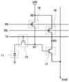
도 2는 본 발명의 일 실시예에 따른 이미지 센서에서 사용되는 단위 픽셀의 회로도이다. 도 3은 도 2에 도시된 선택 트랜지스터와 소오스 팔로워 트랜지스터를 설명하기 위한 단면도이다. 도 4는 MOS 트랜지스터에서의 포화 영역과 선형 영역을 설명하기 위한 도면이다. 도 2에서는 설명의 편의상 4개의 트랜지스터를 포함하는 단위 픽셀을 예로 들고 있으나, 본 발명이 이에 한정되는 것은 아니다. 예를 들어, 본 발명은 3개의 트랜지스터를 포함하는 단위 픽셀 또는, 5개의 트랜지스터를 포함하는 단위 픽셀에 적용할 수도 있다.2 is a circuit diagram of a unit pixel used in an image sensor according to an embodiment of the present invention. 3 is a cross-sectional view illustrating the selection transistor and the source follower transistor illustrated in FIG. 2. 4 is a diagram for describing a saturation region and a linear region in a MOS transistor. In FIG. 2, for convenience of description, a unit pixel including four transistors is taken as an example, but the present invention is not limited thereto. For example, the present invention may be applied to a unit pixel including three transistors or a unit pixel including five transistors.
우선, 도 2를 참조하면, 단위 픽셀(P)이 행렬 형태로 배열되어 APS 어레이(도 1의 10)를 구성한다. 이러한 단위 픽셀(P)은 광전 변환 소자(11), 전송 트랜지스터(15), 소오스 팔로워 트랜지스터(17), 리셋 트랜지스터(18), 선택 트랜지스터(19)를 포함한다.First, referring to FIG. 2, the unit pixels P are arranged in a matrix to form an APS array (10 of FIG. 1). The unit pixel P includes a
광전 변환 소자(11)는 입사광에 응답하여 광량에 대응하는 전하를 축적한다. 광전 변환 소자(11)는 포토 다이오드, 포토 트랜지스터, 포토 게이트, 핀드 포토 다이오드 또는 이들의 조합이 적용될 수 있으며, 도면에는 포토 다이오드가 예시되어 있다.The
광전 변환 소자(11)는 축적된 전하를 검출 노드(N1)로 전송하는 전송 트랜지스터(15)와 전기적으로 연결된다. 검출 노드(N1)는 전기적으로 플로팅되어 있는 상태이므로, 플로팅 확산 영역(Floating Diffusion region)으로 불리기도 한다. 검출 노드(N1)는 기생 커패시턴스를 갖고 있기 때문에, 전하가 누적적으로 저장된다.The
리셋 트랜지스터(18)는 검출 노드(N1)을 주기적으로 리셋시킨다. 리셋 트랜지스터(18)는 검출 노드(N1)와 전압 노드(N2) 사이에 커플링되고, 게이트로 리셋 신호(RX)를 제공받아 구동된다. 리셋 트랜지스터(18)가 리셋 신호(RX)에 의해 턴온되면, 전압 노드(N2)에 인가되고 있는 소정 전압, 예를 들어, 전원 전압(VDD)가 검출 노드(N1)로 전달되어 검출 노드(N1)를 리셋하게 된다.The
선택 트랜지스터(19)는 단위 픽셀(P)을 선택하는 역할을 한다. 선택 트랜지스터(19)는 소오스 팔로워 트랜지스터(17)와 전압 노드(N2) 사이에 커플링되고, 게이트로 선택 신호(SEL)를 제공받아 구동된다.The
소오스 팔로워 트랜지스터(17)는 검출 노드(N1)의 전류를 증폭하고, 증폭된 출력 신호를 출력 라인(Vout)으로 출력한다. 구체적으로, 소오스 팔로워 트랜지스터(17)는 전류 소오스(current source)(미도시)와 커플링되어 있어 일정한 레벨의 전류를 흐르게 하기 때문에, 소오스 팔로워 트랜지스터(17)의 소오스 전압은 게이트 전압에 비례하여 변하게 된다. 이와 같이 변하는 소오스 전압을 상관 이중 샘플 러(50)가 센싱하게 된다. 따라서, 소오스 전압과 게이트 전압은 서로 비례 관계(특히, 선형 관계)를 갖는 것이 중요하다. 또한, 소오스 전압과 게이트 전압이 선형 관계를 가질려면, 소오스 팔로워 트랜지스터(17)는 포화 영역에서 동작해야 한다.The
이에 대해서 구체적으로 설명하면 다음과 같다. 도 4에 도시된 바와 같이, 포화 영역(A)은 게이트-소오스간 전압(VGS)에서 문턱 전압(Vth)을 뺀 값이, 드레인-소오스간 전압(VDS)보다 작은 영역을 의미하고, 선형 영역(B)은 게이트-소오스간 전압(VGS)에서 문턱 전압(Vth)을 뺀 값이, 드레인-소오스간 전압(VDS)보다 큰 영역을 의미한다. 한편, 포화 영역(A)과 선형 영역(B) 사이의 경계(C)는 핀치 오프 포인트(pinch-off point)라고도 불리고, 게이트-소오스간 전압(VGS)에서 문턱 전압(Vth)을 뺀 값이 드레인-소오스간 전압(VDS)과 동일한 부분을 의미한다.This will be described in detail as follows. As illustrated in FIG. 4, the saturation region A refers to a region in which a value obtained by subtracting the threshold voltage Vth from the gate-source voltage VGS is smaller than the drain-source voltage VDS . The linear region B refers to a region in which a value obtained by subtracting the threshold voltage Vth from the gate-source voltage VGS is greater than the drain-source voltage VDS . The boundary C between the saturation region A and the linear region B is also called a pinch-off point, and is obtained by subtracting the threshold voltage Vth from the gate-source voltage VGS . It means the same part as the drain-source voltage VDS .
MOS 트랜지스터가 포화 영역(A)에서 동작할 경우의 드레인 전류(ID)는 수학식 1과 같이 표현될 수 있고, 선형 영역(B)에서 동작할 경우의 드레인 전류(ID)는 수학식 2와 같이 표현될 수 있다. 수학식 1을 참조하면 포화 영역(A)에서 드레인 전류(ID)의 크기는 게이트-소오스간 전압(VGS)에 의해서 결정되지만, 수학식 2를 참조하면 선형 영역(B)에서 드레인 전류(ID)의 크기는 게이트-소오스간 전압(VGS)뿐만 아니라 드레인-소오스간 전압(VDS)에 의해서 결정되게 된다. 달리 표현하면, 드레인 전류(ID)가 일정할 때, 소오스 팔로워 트랜지스터(17)가 포화 영역(A)에서 동작하면 소오스 전압은 게이트 전압(VG)에 의해서만 영향을 받지만, 소오스 팔로워 트랜지스터(17)가 선형 영역(B)에서 동작하면 소오스 전압은 게이트 전압(VG)뿐만 아니라 드레인 전압(VD)에 의해서도 영향을 받게 된다. 따라서, 소오스 팔로워 트랜지스터(17)의 소오스 전압(VS)과 게이트 전압(VG)이 선형 관계를 가질려면, 소오스 팔로워 트랜지스터(17)는 포화 영역(A)에서 동작해야 한다.The drain current ID when the MOS transistor operates in the saturation region A may be represented by
한편, 선택 트랜지스터(19)가 소오스 팔로워 트랜지스터(17)와 전압 노드(N2) 사이에 배치되어 있으면, PSRR(Power Supply Rejection Ratio) 특성이 향상된다. PSRR 특성에 대해서 자세히 설명하면 다음과 같다. 소오스 팔로워 트랜지스터(17)는 안정적으로 동작하여 노이즈 없는 출력 신호를 생성해야 한다. 그런데, 소오스 팔로워 트랜지스터(17)가 전원 전압(VDD)이 인가되고 있는 전압 노드(N2)와 직접 커플링되어 있다면, 전원 전압(VDD)이 흔들리면 소오스 팔로워 트랜지스터(17)가 출력하는 출력 신호에도 노이즈가 발생할 수 있다. 그런데, 소오스 팔로워 트랜지스터(17)와 전압 노드(N2) 사이에 배치되어 있는 선택 트랜지스터(19)는, 전원 전압(VDD)의 흔들림이 소오스 팔로워 트랜지스터(17)에 전달되는 것을 방지한다.On the other hand, when the
반면, 선택 트랜지스터(19)가 소오스 팔로워 트랜지스터(17)와 전압 노드(N2) 사이에 배치되어 있으면, 소오스 팔로워 트랜지스터(17)가 포화 영역(A)과 선형 영역(B)의 경계에서 동작하게 되어, 동작이 불안정하게 될 수 있다. 즉, 소오스 팔로워 트랜지스터(17)의 선형성 특성(linearity characteristics)이 떨어질 수 있다. 이에 대해서 예를 들어 자세히 설명하면 다음과 같다.On the other hand, if the
소오스 팔로워 트랜지스터(17) 및 선택 트랜지스터(19)는 증가형(enhancement type) 트랜지스터이고, 리셋 트랜지스터(18)는 공핍형(depletion type) 트랜지스터일 수 있다. 전압 노드(N2)에 인가되고 있는 전원 전압(VDD)의 레벨이 약 2.8V이고, 트랜지스터의 문턱 전압(Vth)의 레벨은 약 0.6V인 경우를 예로 든다.The
리셋 트랜지스터(18)가 검출 노드(N1)를 리셋하면, 검출 노드(N1)의 전압 레벨은 2.8V가 된다. 반면, 노드(N3)의 전압 레벨은 전원 전압(VDD)에서 선택 트랜지스터(19)의 문턱 전압(Vth)을 뺀 값과 동일해 지므로, 2.2V (= VDD-Vth = 2.8V-0.6V)가 된다.When the
아래의 수학식 3을 참고하면, 소오스 팔로워 트랜지스터(17)의 게이트-소오스간 전압(VGS)에서 문턱 전압(Vth)을 뺀 값과, 드레인-소오스간 전압(VDS)은 서로 동일하게 된다. 즉, 소오스 팔로워 트랜지스터(17)는 포화 영역(A)과 선형 영역(B) 의 경계에서 동작하게 된다. 따라서, 소오스 팔로워 트랜지스터(17)는 검출 노드(N1)의 전압(즉, 게이트 전압)에 비례하는 출력 신호(즉, 소오스 전압)를 생성할 수 없게 된다.Referring to
VDS = VD - VS = 2.2V - VSVDS = VD-VS = 2.2 V-VS
∴ VGS - Vth = VDSGS VGS -Vth = VDS
그런데, 본 발명의 일 실시예에 따른 이미지 센서에서, 소오스 팔로워 트랜지스터(17)의 게이트는 제1 일함수를 갖는 물질로 이루어지고, 선택 트랜지스터(19)의 게이트는 상기 제1 일함수보다 낮은 제2 일함수를 갖는 물질로 이루어질 수 있다. 도 3에 도시된 바와 같이, 제1 일함수를 갖는 물질로는 제1 도전형(예를 들어, P형)의 도펀트가 도핑된 반도체 물질을 예로 들 수 있고, 제2 일함수를 갖는 물질로는 제1 도전형과 다른 제2 도전형(예를 들어, N형)의 도펀트가 도핑된 반도체 물질을 예로 들 수 있다. 이와 같은 구성으로 인해서, 소오스 팔로워 트랜지스터(17)는 포화 영역에서 안정적으로 동작할 수 있다.However, in the image sensor according to the exemplary embodiment, the gate of the
구체적으로 설명하면, 선택 트랜지스터(19)는 제2 도전형의 도펀트가 도핑된 게이트(120)와, 제2 도전형의 도펀트가 도핑된 소오스/드레인(102, 104)과, 제1 도전형의 도펀트가 도핑된 채널(112)을 포함한다. 소오스 팔로워 트랜지스터(17)는 제1 도전형의 도펀트가 도핑된 게이트(130)와, 제2 도전형의 도펀트가 도핑된 소오 스/드레인(104, 106)과, 제1 도전형의 도펀트가 도핑된 채널(116)을 포함한다.Specifically, the
선택 트랜지스터(19) 및 소오스 팔로워 트랜지스터(17)는 전자(electron)에 의해서 채널(112, 116)이 형성되기 때문에 NMOS 트랜지스터이고, 증가형 트랜지스터일 수 있다. 채널(112, 116)에 제1 도전형(예를 들어, P형) 도펀트를 도핑함으로써 MOS 트랜지스터의 문턱 전압을 상승시킬 수 있다. 이에 따라, MOS 트랜지스터가 턴오프 상태에서는 전자의 흐름을 확실히 차단할 수 있다.The
한편, 소오스 팔로워 트랜지스터(17)의 게이트에는 제1 도전형의 도펀트가 도핑되어 있으므로, 게이트에 제2 도전형의 도펀트가 도핑되어 있는 경우와 비교할 때, 채널(112, 116)을 형성하기 위해서는 더 높은 레벨의 전압이 인가되어야 한다. 즉, 소오스 팔로워 트랜지스터(17)는 문턱 전압이 더 상승되는 효과를 얻을 수 있다. 예를 들어, 제2 도전형의 도펀트가 도핑되어 있는 게이트를 갖는 선택 트랜지스터(19)의 문턱 전압이 Vth라고 하면, 제1 도전형의 도펀트가 도핑되어 있는 게이트를 갖는 소오스 팔로워 트랜지스터(17)의 문턱 전압은 Vth+ΔΦ가 될 수 있다. 여기서, ΔΦ는 Φ1 - Φ2를 의미하고, Φ1은 게이트에 제1 도전형의 도펀트가 도핑되어 있는 경우의 일함수이고, Φ2는 게이트에 제2 도전형의 도펀트가 도핑되어 있는 경우의 일함수를 의미한다. 이웃하는 선택 트랜지스터(19)의 게이트에는 제2 도전형의 도펀트가 도핑되어 있고, 소오스 팔로워 트랜지스터(17)의 게이트에는 제1 도전형의 도펀트가 도핑되어 있으므로, 소오스 팔로워 트랜지스터(17)의 문턱 전압이 선택 트랜지스터(19)의 문턱 전압보다 높게 된다.On the other hand, since the first conductive dopant is doped in the gate of the
이에 따라, 소오스 팔로워 트랜지스터(17)가 포화 영역(A)에서 안정적으로 동작하게 된다. 즉, 소오스 팔로워 트랜지스터(17)의 선형성 특성(linearity characteristics)을 향상시킬 수 있다. 예를 들어 자세히 설명하면 다음과 같다.As a result, the
소오스 팔로워 트랜지스터(17) 및 선택 트랜지스터(19)는 증가형(enhancement type) 트랜지스터이고, 리셋 트랜지스터(18)는 공핍형(depletion type) 트랜지스터일 수 있다. 전압 노드(N2)에 인가되고 있는 전원 전압(VDD)의 레벨이 약 2.8V이고, 선택 트랜지스터(19)의 문턱 전압의 레벨은 약 0.6V이고, 소오스 팔로워 트랜지스터(17)의 문턱 전압의 레벨은 약 0.6V+ΔΦ인 경우를 예로 든다.The
리셋 트랜지스터(18)가 검출 노드(N1)를 리셋하면, 검출 노드(N1)의 전압 레벨은 2.8V가 된다. 반면, 노드(N3)의 전압 레벨은 전원 전압(VDD)에서 선택 트랜지스터(19)의 문턱 전압(Vth)을 뺀 값과 동일해 지므로, 2.2V (= VDD-Vth = 2.8V-0.6V)가 된다.When the
아래의 수학식 4를 참고하면, 소오스 팔로워 트랜지스터(17)의 게이트-소오스간 전압(VGS)에서 문턱 전압(Vth+ΔΦ)을 뺀 값이, 드레인-소오스간 전압(VDS)보다 작게 된다. 즉, 소오스 팔로워 트랜지스터(17)는 포화 영역(A)에서 동작하게 된다. 따라서, 소오스 팔로워 트랜지스터(17)는 검출 노드(N1)의 전압(즉, 게이트 전압)에 비례하는 출력 신호(즉, 소오스 전압)를 생성할 수 있다.Referring to
VDS = VD - VS = 2.2V - VSVDS = VD-VS = 2.2 V-VS
∴ VGS - Vth < VDSGS VGS -Vth <VDS
도 5는 본 발명의 다른 실시예에 따른 이미지 센서에서 사용되는 단위 픽셀의 회로도이다.5 is a circuit diagram of a unit pixel used in an image sensor according to another exemplary embodiment of the present invention.
도 5를 참조하면, 본 발명의 다른 실시예에 따른 이미지 센서가 도 3과 다른 점은, 전압 노드(N2)에 인가되는 전압이 전원 전압보다 높은 레벨을 갖는 승압 전압(VPP)를 사용한다는 점이다. 즉, 리셋 트랜지스터(18)는 검출 노드(N1)를 승압 전압(VPP)을 이용하여 리셋하게 된다.Referring to FIG. 5, an image sensor according to another exemplary embodiment of the present invention is different from FIG. 3 in that a voltage applied to the voltage node N2 uses a boosted voltage VPP having a level higher than a power supply voltage. to be. That is, the
또한, 전송 트랜지스터(15)는 승압 전압(VPP) 레벨의 전송 신호에 응답하여, 광전 변환 소자(11)에 축적된 전하를 검출 노드(N1)로 전달할 수 있다.In addition, the
이와 같이 할 경우, 광전 변환 소자(11)에 축적된 전하를 검출 노드(N1)로 완전히 전달할 수 있어, 이미지 래그(image lag) 현상을 없앨 수 있다.In this case, the charge accumulated in the
그런데, 선택 트랜지스터(19)는 승압 전압(VPP)보다 낮은 레벨의 선택 신호(SEL)에 응답하여 동작할 수 있다.However, the
반면, 선택 트랜지스터(19)가 소오스 팔로워 트랜지스터(17)와 전압 노드(N2) 사이에 배치되어 있으면, 소오스 팔로워 트랜지스터(17)가 선형 영역(linear region)에서 동작할 수 있는데, 본 발명의 다른 실시예에 따른 이미지 센서에서 소오스 팔로워 트랜지스터(17)의 게이트에 제1 도전형의 도펀트를 도핑함 으로써 소오스 팔로워 트랜지스터(17)가 포화 영역에서 동작할 수 있도록 한다.On the other hand, if the
소오스 팔로워 트랜지스터(17) 및 선택 트랜지스터(19)는 증가형(enhancement type) 트랜지스터이고, 리셋 트랜지스터(18)는 공핍형(depletion type) 트랜지스터일 수 있다. 전압 노드(N2)에 인가되고 있는 승압 전압(VDD)의 레벨이 약 3.3V이고, 선택 트랜지스터(19)에 인가되고 있는 선택 신호(RX)는 전원 전압(VDD) 레벨(약 2.8V)이고, 선택 트랜지스터(19)의 문턱 전압의 레벨은 약 0.6V이고, 소오스 팔로워 트랜지스터(17)의 문턱 전압의 레벨은 약 0.6V+ΔΦ인 경우를 예로 든다.The
리셋 트랜지스터(18)가 검출 노드(N1)를 리셋하면, 검출 노드(N1)의 전압 레벨은 3.3V가 된다. 반면, 노드(N3)의 전압 레벨은 선택 신호(RX)의 전압 레벨에서 선택 트랜지스터(19)의 문턱 전압(Vth)을 뺀 값과 동일해 지므로, 2.2V(= 2.8V-0.6V)가 된다.When the
아래의 수학식 5를 참고하면, ΔΦ가 0.5V보다 크게 되면, 소오스 팔로워 트랜지스터(17)의 게이트-소오스간 전압(VGS)에서 문턱 전압(Vth+ΔΦ)을 뺀 값이, 드레인-소오스간 전압(VDS)보다 작게 된다. 즉, 소오스 팔로워 트랜지스터(17)는 포화 영역에서 동작하게 된다. 따라서, 소오스 팔로워 트랜지스터(17)는 검출 노드(N1)의 전압(즉, 게이트 전압)에 비례하는 출력 신호(즉, 소오스 전압)를 생성할 수 있다.Referring to Equation 5 below, when ΔΦ is greater than 0.5V, a value obtained by subtracting the threshold voltage Vth + ΔΦ from the gate-source voltage VGS of the
VDS = VD - VS = 2.2V - VSVDS = VD-VS = 2.2 V-VS
∴ VGS - Vth < VDS(ΔΦ가 0.5V보다 큰 경우)GS VGS -Vth <VDS (When ΔΦ is greater than 0.5 V)
도 6a 및 도 6b는 본 발명의 일 실시예에 따른 이미지 센서의 제조 방법을 설명하기 위한 단면도이다. 도 6a 및 도 6b에서는 단위 픽셀의 다른 구성 요소에 대한 도시는 생략하고, 소오스 팔로워 트랜지스터만을 도시하였다.6A and 6B are cross-sectional views illustrating a method of manufacturing an image sensor according to an embodiment of the present invention. In FIGS. 6A and 6B, only the source follower transistors are illustrated and other components of the unit pixel are omitted.
우선, 도 6a을 참조하면, 제1 도전형(예를 들어, P형)의 기판(100) 내에 제1 도전형의 불순물을 이온 주입하여 채널(116)을 형성한다. 전술한 바와 같이, 채널(116)에 제1 도전형의 불순물을 이온 주입함으로써 소오스 팔로워 트랜지스터(17)의 문턱 전압을 상승시킬 수 있다.First, referring to FIG. 6A, the
이어서, 기판(100) 상에 게이트(130a)를 형성한다.Subsequently, a
이어서, 게이트(130a)의 양측의 기판(100) 내에 제2 도전형(예를 들어, N형)의 불순물을 이온 주입하여 저농도 불순물 영역을 형성한다.Subsequently, impurities of a second conductivity type (eg, N type) are ion-implanted into the
이어서, 게이트(130a)의 양측벽에 스페이서를 형성한다.Subsequently, spacers are formed on both side walls of the
이어서, 게이트(130a)의 양측의 기판(100) 내에 제2 도전형의 불순물을 이온 주입(180)하여 고농도 불순물 영역을 형성하여, 소오스/드레인(104, 106)을 완성한다. 도면에서는 소오스/드레인(104, 106)이 LDD(Low Doped Drain) 형태인 경우를 예로 들었으나, 본 발명이 이에 한정되는 것은 아니다. 여기서, 게이트(130a)를 마 스크 패턴(141)으로 블로킹하여, 게이트(130a)에는 제2 도전형의 불순물이 이온 주입되지 않도록 한다.Subsequently, a high concentration impurity region is formed by ion implanting 180 a second conductivity type impurity into the
도 6b를 참조하면, 게이트(130a)에 제1 도전형의 불순물을 이온 주입(182)하여 소오스 팔로워 트랜지스터를 완성한다. 여기서, 소오스/드레인(104, 106)를 마스크 패턴(142)으로 블로킹하여, 소오스/드레인(104, 106)에는 제1 도전형의 불순물이 이온 주입되지 않도록 한다.Referring to FIG. 6B, a source follower transistor is completed by ion implanting 182 a first conductivity type impurity into the
도 7은 본 발명의 다른 실시예에 따른 이미지 센서의 제조 방법을 설명하기 위한 단면도이다.7 is a cross-sectional view illustrating a method of manufacturing an image sensor according to another exemplary embodiment of the present invention.
도 7을 참조하면, 전술하였던 도 6b에서 소오스 팔로워 트랜지스터(17)의 게이트(130)에 제1 도전형의 불순물을 이온 주입(183)하는 것은, 기판(100)의 주변 회로 영역 상에 형성된 게이트(132)와, 게이트(132)의 양측의 기판(100) 내에 제1 도전형의 불순물을 이온 주입(183)하는 것과 동시에 이루어질 수 있다. 이와 같이 하면, 소오스 팔로워 트랜지스터(17)의 게이트(130)를 블로킹하기 위한 별도의 마스크 패턴을 사용하지 않아도 되기 때문에, 제조 과정 중에 사용되는 마스크 숫자가 증가되지 않는다.Referring to FIG. 7, the
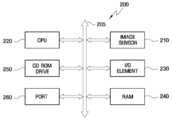
도 8은 본 발명의 실시예들에 따른 이미지 센서를 포함하는 프로세서 기반 시스템을 나타내는 개략적 블록도이다.8 is a schematic block diagram illustrating a processor based system including an image sensor according to embodiments of the present disclosure.
도 8을 참조하면, 프로세서 기반 시스템(200)은 CMOS 이미지 센서(210)의 출력 이미지를 처리하는 시스템이다. 시스템(200)은 컴퓨터 시스템, 카메라 시스템, 스캐너, 기계화된 시계 시스템, 네비게이션 시스템, 비디오폰, 감독 시스템, 자동 포커스 시스템, 추적 시스템, 동작 감시 시스템, 이미지 안정화 시스템 등을 예시할 수 있으나, 이에 제한되는 것은 아니다.Referring to FIG. 8, the processor-based
컴퓨터 시스템 등과 같은 프로세서 기반 시스템(200)은 버스(205)를 통해 입출력(I/O) 소자(230)와 커뮤니케이션할 수 있는 마이크로프로세서 등과 같은 중앙 정보 처리 장치(CPU)(220)를 포함한다. CMOS 이미지 센서(210)는 버스(205) 또는 다른 통신 링크를 통해서 시스템과 커뮤니케이션할 수 있다. 또, 프로세서 기반 시스템(200)은 버스(205)를 통해 CPU(220)와 커뮤니케이션할 수 있는 RAM(240), CD ROM 드라이브(250) 및/또는 포트(260)를 더 포함할 수 있다. 포트(260)는 비디오 카드, 사운드 카드, 메모리 카드, USB 소자 등을 커플링하거나, 또 다른 시스템과 데이터를 통신할 수 있는 포트일 수 있다. CMOS 이미지 센서(210)는 CPU, 디지털 신호 처리 장치(DSP) 또는 마이크로프로세서 등과 함께 집적될 수 있다. 또, 메모리가 함께 집적될 수도 있다. 물론 경우에 따라서는 프로세서와 별개의 칩에 집적될 수도 있다.Processor-based
이상 첨부된 도면을 참조하여 본 발명의 실시예를 설명하였지만, 본 발명이 속하는 기술분야에서 통상의 지식을 가진 자는 본 발명이 그 기술적 사상이나 필수적인 특징을 변경하지 않고서 다른 구체적인 형태로 실시될 수 있다는 것을 이해할 수 있을 것이다. 그러므로 이상에서 기술한 실시예들은 모든 면에서 예시적인 것이며 한정적이 아닌 것으로 이해해야만 한다.While the present invention has been described in connection with what is presently considered to be practical exemplary embodiments, it is to be understood that the invention is not limited to the disclosed embodiments, but, on the contrary, You will understand. It is therefore to be understood that the above-described embodiments are illustrative in all aspects and not restrictive.
도 1은 본 발명의 실시예들에 따른 이미지 센서의 블록도이다.1 is a block diagram of an image sensor according to example embodiments.
도 2는 본 발명의 일 실시예에 따른 이미지 센서에서 사용되는 단위 픽셀의 회로도이다.2 is a circuit diagram of a unit pixel used in an image sensor according to an embodiment of the present invention.
도 3은 도 2에 도시된 선택 트랜지스터와 소오스 팔로워 트랜지스터를 설명하기 위한 단면도이다.3 is a cross-sectional view illustrating the selection transistor and the source follower transistor illustrated in FIG. 2.
도 4는 MOS 트랜지스터에서의 포화 영역과 선형 영역을 설명하기 위한 도면이다.4 is a diagram for describing a saturation region and a linear region in a MOS transistor.
도 5는 본 발명의 다른 실시예에 따른 이미지 센서에서 사용되는 단위 픽셀의 회로도이다.5 is a circuit diagram of a unit pixel used in an image sensor according to another exemplary embodiment of the present invention.
도 6a 및 도 6b는 본 발명의 일 실시예에 따른 이미지 센서의 제조 방법을 설명하기 위한 단면도이다.6A and 6B are cross-sectional views illustrating a method of manufacturing an image sensor according to an embodiment of the present invention.
도 7은 본 발명의 다른 실시예에 따른 이미지 센서의 제조 방법을 설명하기 위한 단면도이다.7 is a cross-sectional view illustrating a method of manufacturing an image sensor according to another exemplary embodiment of the present invention.
도 8은 본 발명의 실시예들에 따른 이미지 센서를 포함하는 프로세서 기반 시스템을 나타내는 개략적 블록도이다.8 is a schematic block diagram illustrating a processor based system including an image sensor according to embodiments of the present disclosure.
(도면의 주요부분에 대한 부호의 설명)DESCRIPTION OF THE REFERENCE NUMERALS (S)
10 : APS 어레이11 : 광전 변환 소자10: APS array 11: Photoelectric conversion element
15 : 전송 트랜지스터17 : 소오스 팔로워 트랜지스터15: transfer transistor 17: source follower transistor
18 : 리셋 트랜지스터19 : 선택 트랜지스터18: reset transistor 19: select transistor
130, 130a : 게이트104, 106 : 소오스/드레인130, 130a:
116 : 채널116: channel
Claims (26)
Translated fromKoreanPriority Applications (2)
| Application Number | Priority Date | Filing Date | Title |
|---|---|---|---|
| KR1020070071330AKR101344441B1 (en) | 2007-07-16 | 2007-07-16 | Image sensor and fabricating method thereof |
| US12/218,287US8068157B2 (en) | 2007-07-16 | 2008-07-14 | Image sensor with wide operating range |
Applications Claiming Priority (1)
| Application Number | Priority Date | Filing Date | Title |
|---|---|---|---|
| KR1020070071330AKR101344441B1 (en) | 2007-07-16 | 2007-07-16 | Image sensor and fabricating method thereof |
Publications (2)
| Publication Number | Publication Date |
|---|---|
| KR20090008041A KR20090008041A (en) | 2009-01-21 |
| KR101344441B1true KR101344441B1 (en) | 2013-12-23 |
Family
ID=40294971
Family Applications (1)
| Application Number | Title | Priority Date | Filing Date |
|---|---|---|---|
| KR1020070071330AActiveKR101344441B1 (en) | 2007-07-16 | 2007-07-16 | Image sensor and fabricating method thereof |
Country Status (2)
| Country | Link |
|---|---|
| US (1) | US8068157B2 (en) |
| KR (1) | KR101344441B1 (en) |
Families Citing this family (14)
| Publication number | Priority date | Publication date | Assignee | Title |
|---|---|---|---|---|
| KR20090087644A (en)* | 2008-02-13 | 2009-08-18 | 삼성전자주식회사 | According to the pixel circuit array |
| US8760631B2 (en)* | 2010-01-27 | 2014-06-24 | Intersil Americas Inc. | Distance sensing by IQ domain differentiation of time of flight (TOF) measurements |
| WO2011116345A1 (en)* | 2010-03-19 | 2011-09-22 | Invisage Technologies, Inc. | Dark current reduction in image sensors via dynamic electrical biasing |
| JP5885401B2 (en) | 2010-07-07 | 2016-03-15 | キヤノン株式会社 | Solid-state imaging device and imaging system |
| JP5643555B2 (en) | 2010-07-07 | 2014-12-17 | キヤノン株式会社 | Solid-state imaging device and imaging system |
| JP5751766B2 (en)* | 2010-07-07 | 2015-07-22 | キヤノン株式会社 | Solid-state imaging device and imaging system |
| JP5656484B2 (en) | 2010-07-07 | 2015-01-21 | キヤノン株式会社 | Solid-state imaging device and imaging system |
| JP5697371B2 (en) | 2010-07-07 | 2015-04-08 | キヤノン株式会社 | Solid-state imaging device and imaging system |
| KR102131327B1 (en) | 2013-08-16 | 2020-07-07 | 삼성전자 주식회사 | Image sensor comprising source follower |
| WO2016019258A1 (en) | 2014-07-31 | 2016-02-04 | Emanuele Mandelli | Image sensors with noise reduction |
| US20160099283A1 (en)* | 2014-10-03 | 2016-04-07 | Omnivision Technologies, Inc. | Photosensor with channel region having center contact |
| WO2017219223A1 (en)* | 2016-06-21 | 2017-12-28 | Shenzhen Genorivision Technology Co. Ltd. | An image sensor with large dynamic range |
| US10425601B1 (en) | 2017-05-05 | 2019-09-24 | Invisage Technologies, Inc. | Three-transistor active reset pixel |
| CN112752042A (en)* | 2020-12-30 | 2021-05-04 | 长春长光辰芯光电技术有限公司 | Row driver and image sensor formed by same |
Citations (3)
| Publication number | Priority date | Publication date | Assignee | Title |
|---|---|---|---|---|
| JP3487575B2 (en) | 1997-12-26 | 2004-01-19 | キヤノン株式会社 | Photoelectric conversion device |
| JP2004241498A (en) | 2003-02-04 | 2004-08-26 | Mitsubishi Electric Corp | Solid-state imaging device and operation method thereof |
| KR100642451B1 (en) | 2005-11-07 | 2006-11-02 | 매그나칩 반도체 유한회사 | CMOS image sensor and its manufacturing method |
Family Cites Families (15)
| Publication number | Priority date | Publication date | Assignee | Title |
|---|---|---|---|---|
| US5614744A (en)* | 1995-08-04 | 1997-03-25 | National Semiconductor Corporation | CMOS-based, low leakage active pixel array with anti-blooming isolation |
| JP4681767B2 (en)* | 2001-07-17 | 2011-05-11 | キヤノン株式会社 | Imaging device and camera |
| JP4434530B2 (en)* | 2001-09-17 | 2010-03-17 | ソニー株式会社 | Solid-state imaging device |
| US6744084B2 (en)* | 2002-08-29 | 2004-06-01 | Micro Technology, Inc. | Two-transistor pixel with buried reset channel and method of formation |
| JP3795846B2 (en)* | 2002-08-29 | 2006-07-12 | 富士通株式会社 | Semiconductor device |
| JP4207659B2 (en)* | 2003-05-16 | 2009-01-14 | ソニー株式会社 | Solid-state imaging device, driving method thereof, and camera device |
| US7652704B2 (en)* | 2004-08-25 | 2010-01-26 | Aptina Imaging Corporation | Pixel for boosting pixel reset voltage |
| US7442970B2 (en)* | 2004-08-30 | 2008-10-28 | Micron Technology, Inc. | Active photosensitive structure with buried depletion layer |
| JP4513497B2 (en)* | 2004-10-19 | 2010-07-28 | ソニー株式会社 | Solid-state imaging device |
| US7446807B2 (en)* | 2004-12-03 | 2008-11-04 | Micron Technology, Inc. | Imager pixel with capacitance for boosting reset voltage |
| JP5114829B2 (en)* | 2005-05-13 | 2013-01-09 | ソニー株式会社 | Semiconductor device and manufacturing method thereof |
| JP2006352341A (en)* | 2005-06-14 | 2006-12-28 | Micron Technol Inc | Anti-Eclipse circuit and its operation method |
| JP4747781B2 (en)* | 2005-10-27 | 2011-08-17 | 船井電機株式会社 | Imaging device |
| JP4650249B2 (en)* | 2005-12-13 | 2011-03-16 | 船井電機株式会社 | Imaging device |
| US7470946B2 (en)* | 2006-03-17 | 2008-12-30 | Sharp Laboratories Of America, Inc. | Triple-junction filterless CMOS color imager cell |
- 2007
- 2007-07-16KRKR1020070071330Apatent/KR101344441B1/enactiveActive
- 2008
- 2008-07-14USUS12/218,287patent/US8068157B2/enactiveActive
Patent Citations (3)
| Publication number | Priority date | Publication date | Assignee | Title |
|---|---|---|---|---|
| JP3487575B2 (en) | 1997-12-26 | 2004-01-19 | キヤノン株式会社 | Photoelectric conversion device |
| JP2004241498A (en) | 2003-02-04 | 2004-08-26 | Mitsubishi Electric Corp | Solid-state imaging device and operation method thereof |
| KR100642451B1 (en) | 2005-11-07 | 2006-11-02 | 매그나칩 반도체 유한회사 | CMOS image sensor and its manufacturing method |
Also Published As
| Publication number | Publication date |
|---|---|
| US20090027529A1 (en) | 2009-01-29 |
| KR20090008041A (en) | 2009-01-21 |
| US8068157B2 (en) | 2011-11-29 |
Similar Documents
| Publication | Publication Date | Title |
|---|---|---|
| KR101344441B1 (en) | Image sensor and fabricating method thereof | |
| US7541571B2 (en) | Image sensor having first and second charge transmitters | |
| JP5538876B2 (en) | Solid-state imaging device | |
| JP5316606B2 (en) | Solid-state imaging device and manufacturing method thereof | |
| US20070269944A1 (en) | CMOS image sensor | |
| US7612819B2 (en) | CMOS image sensor and method of operating the same | |
| JP2008258885A (en) | Imaging apparatus and driving method of imaging apparatus | |
| KR20090050252A (en) | Image sensor | |
| KR101374301B1 (en) | Image sensor | |
| US20120132786A1 (en) | Solid state imaging device | |
| US20050017155A1 (en) | Active pixel cell using negative to positive voltage swing transfer transistor | |
| JP4654046B2 (en) | Clamp circuit for CMOS image sensor | |
| US20090078975A1 (en) | CMOS image sensor | |
| US9006639B2 (en) | Pixel architecture with the control terminal of a first switch coupled to the control terminal of a second switch and method | |
| US20070096233A1 (en) | Cmos image sensor | |
| KR20020057282A (en) | Image sensor capable of preventing flowing backward of charge | |
| JP2006100761A (en) | Solid-state image sensing device and its manufacturing method, and its driving method | |
| KR100421121B1 (en) | Method for operating a pixel circuit of a cmos image sensor | |
| US12273105B2 (en) | Voltage generation circuit, image sensor, scope, and voltage generation method | |
| JP4618170B2 (en) | Solid-state imaging device | |
| US20160088244A1 (en) | Switching circuit, sample and hold circuit, and solid-state imaging device | |
| JP2010171318A (en) | Solid-state imaging device, imaging apparatus, and signal reading method of the solid-state imaging device | |
| JP3585898B2 (en) | Camera using CCD solid-state imaging device | |
| KR20070050576A (en) | Image sensor | |
| JP4561651B2 (en) | Solid-state image sensor |
Legal Events
| Date | Code | Title | Description |
|---|---|---|---|
| PA0109 | Patent application | Patent event code:PA01091R01D Comment text:Patent Application Patent event date:20070716 | |
| PG1501 | Laying open of application | ||
| A201 | Request for examination | ||
| PA0201 | Request for examination | Patent event code:PA02012R01D Patent event date:20120704 Comment text:Request for Examination of Application Patent event code:PA02011R01I Patent event date:20070716 Comment text:Patent Application | |
| E902 | Notification of reason for refusal | ||
| PE0902 | Notice of grounds for rejection | Comment text:Notification of reason for refusal Patent event date:20130808 Patent event code:PE09021S01D | |
| E701 | Decision to grant or registration of patent right | ||
| PE0701 | Decision of registration | Patent event code:PE07011S01D Comment text:Decision to Grant Registration Patent event date:20131020 | |
| GRNT | Written decision to grant | ||
| PR0701 | Registration of establishment | Comment text:Registration of Establishment Patent event date:20131217 Patent event code:PR07011E01D | |
| PR1002 | Payment of registration fee | Payment date:20131218 End annual number:3 Start annual number:1 | |
| PG1601 | Publication of registration | ||
| FPAY | Annual fee payment | Payment date:20191129 Year of fee payment:7 | |
| PR1001 | Payment of annual fee | Payment date:20191129 Start annual number:7 End annual number:7 | |
| PR1001 | Payment of annual fee | Payment date:20201130 Start annual number:8 End annual number:8 | |
| PR1001 | Payment of annual fee | Payment date:20221123 Start annual number:10 End annual number:10 | |
| PR1001 | Payment of annual fee | Payment date:20241126 Start annual number:12 End annual number:12 |