KR101341299B1 - Dye-sensitized solar cell - Google Patents
Dye-sensitized solar cellDownload PDFInfo
- Publication number
- KR101341299B1 KR101341299B1KR1020087032191AKR20087032191AKR101341299B1KR 101341299 B1KR101341299 B1KR 101341299B1KR 1020087032191 AKR1020087032191 AKR 1020087032191AKR 20087032191 AKR20087032191 AKR 20087032191AKR 101341299 B1KR101341299 B1KR 101341299B1
- Authority
- KR
- South Korea
- Prior art keywords
- oxide semiconductor
- thin film
- dye
- solar cell
- wavelength region
- Prior art date
- Legal status (The legal status is an assumption and is not a legal conclusion. Google has not performed a legal analysis and makes no representation as to the accuracy of the status listed.)
- Expired - Fee Related
Links
Images


Classifications
- H—ELECTRICITY
- H01—ELECTRIC ELEMENTS
- H01G—CAPACITORS; CAPACITORS, RECTIFIERS, DETECTORS, SWITCHING DEVICES, LIGHT-SENSITIVE OR TEMPERATURE-SENSITIVE DEVICES OF THE ELECTROLYTIC TYPE
- H01G9/00—Electrolytic capacitors, rectifiers, detectors, switching devices, light-sensitive or temperature-sensitive devices; Processes of their manufacture
- H01G9/20—Light-sensitive devices
- H01G9/2068—Panels or arrays of photoelectrochemical cells, e.g. photovoltaic modules based on photoelectrochemical cells
- H01G9/2072—Panels or arrays of photoelectrochemical cells, e.g. photovoltaic modules based on photoelectrochemical cells comprising two or more photoelectrodes sensible to different parts of the solar spectrum, e.g. tandem cells
- H—ELECTRICITY
- H10—SEMICONDUCTOR DEVICES; ELECTRIC SOLID-STATE DEVICES NOT OTHERWISE PROVIDED FOR
- H10F—INORGANIC SEMICONDUCTOR DEVICES SENSITIVE TO INFRARED RADIATION, LIGHT, ELECTROMAGNETIC RADIATION OF SHORTER WAVELENGTH OR CORPUSCULAR RADIATION
- H10F10/00—Individual photovoltaic cells, e.g. solar cells
- H—ELECTRICITY
- H01—ELECTRIC ELEMENTS
- H01G—CAPACITORS; CAPACITORS, RECTIFIERS, DETECTORS, SWITCHING DEVICES, LIGHT-SENSITIVE OR TEMPERATURE-SENSITIVE DEVICES OF THE ELECTROLYTIC TYPE
- H01G9/00—Electrolytic capacitors, rectifiers, detectors, switching devices, light-sensitive or temperature-sensitive devices; Processes of their manufacture
- H01G9/20—Light-sensitive devices
- H01G9/2027—Light-sensitive devices comprising an oxide semiconductor electrode
- H01G9/2036—Light-sensitive devices comprising an oxide semiconductor electrode comprising mixed oxides, e.g. ZnO covered TiO2 particles
- H—ELECTRICITY
- H01—ELECTRIC ELEMENTS
- H01M—PROCESSES OR MEANS, e.g. BATTERIES, FOR THE DIRECT CONVERSION OF CHEMICAL ENERGY INTO ELECTRICAL ENERGY
- H01M14/00—Electrochemical current or voltage generators not provided for in groups H01M6/00 - H01M12/00; Manufacture thereof
- H—ELECTRICITY
- H01—ELECTRIC ELEMENTS
- H01G—CAPACITORS; CAPACITORS, RECTIFIERS, DETECTORS, SWITCHING DEVICES, LIGHT-SENSITIVE OR TEMPERATURE-SENSITIVE DEVICES OF THE ELECTROLYTIC TYPE
- H01G9/00—Electrolytic capacitors, rectifiers, detectors, switching devices, light-sensitive or temperature-sensitive devices; Processes of their manufacture
- H01G9/20—Light-sensitive devices
- H01G9/2027—Light-sensitive devices comprising an oxide semiconductor electrode
- H01G9/2031—Light-sensitive devices comprising an oxide semiconductor electrode comprising titanium oxide, e.g. TiO2
- H—ELECTRICITY
- H01—ELECTRIC ELEMENTS
- H01G—CAPACITORS; CAPACITORS, RECTIFIERS, DETECTORS, SWITCHING DEVICES, LIGHT-SENSITIVE OR TEMPERATURE-SENSITIVE DEVICES OF THE ELECTROLYTIC TYPE
- H01G9/00—Electrolytic capacitors, rectifiers, detectors, switching devices, light-sensitive or temperature-sensitive devices; Processes of their manufacture
- H01G9/20—Light-sensitive devices
- H01G9/2059—Light-sensitive devices comprising an organic dye as the active light absorbing material, e.g. adsorbed on an electrode or dissolved in solution
- H01G9/2063—Light-sensitive devices comprising an organic dye as the active light absorbing material, e.g. adsorbed on an electrode or dissolved in solution comprising a mixture of two or more dyes
- H—ELECTRICITY
- H10—SEMICONDUCTOR DEVICES; ELECTRIC SOLID-STATE DEVICES NOT OTHERWISE PROVIDED FOR
- H10K—ORGANIC ELECTRIC SOLID-STATE DEVICES
- H10K85/00—Organic materials used in the body or electrodes of devices covered by this subclass
- H10K85/30—Coordination compounds
- H10K85/341—Transition metal complexes, e.g. Ru(II)polypyridine complexes
- H10K85/344—Transition metal complexes, e.g. Ru(II)polypyridine complexes comprising ruthenium
- H—ELECTRICITY
- H10—SEMICONDUCTOR DEVICES; ELECTRIC SOLID-STATE DEVICES NOT OTHERWISE PROVIDED FOR
- H10K—ORGANIC ELECTRIC SOLID-STATE DEVICES
- H10K85/00—Organic materials used in the body or electrodes of devices covered by this subclass
- H10K85/60—Organic compounds having low molecular weight
- H10K85/649—Aromatic compounds comprising a hetero atom
- H10K85/652—Cyanine dyes
- Y—GENERAL TAGGING OF NEW TECHNOLOGICAL DEVELOPMENTS; GENERAL TAGGING OF CROSS-SECTIONAL TECHNOLOGIES SPANNING OVER SEVERAL SECTIONS OF THE IPC; TECHNICAL SUBJECTS COVERED BY FORMER USPC CROSS-REFERENCE ART COLLECTIONS [XRACs] AND DIGESTS
- Y02—TECHNOLOGIES OR APPLICATIONS FOR MITIGATION OR ADAPTATION AGAINST CLIMATE CHANGE
- Y02E—REDUCTION OF GREENHOUSE GAS [GHG] EMISSIONS, RELATED TO ENERGY GENERATION, TRANSMISSION OR DISTRIBUTION
- Y02E10/00—Energy generation through renewable energy sources
- Y02E10/50—Photovoltaic [PV] energy
- Y02E10/542—Dye sensitized solar cells
Landscapes
- Engineering & Computer Science (AREA)
- Power Engineering (AREA)
- Microelectronics & Electronic Packaging (AREA)
- Chemical & Material Sciences (AREA)
- Chemical Kinetics & Catalysis (AREA)
- Electrochemistry (AREA)
- Life Sciences & Earth Sciences (AREA)
- Sustainable Development (AREA)
- General Chemical & Material Sciences (AREA)
- Hybrid Cells (AREA)
- Photovoltaic Devices (AREA)
Abstract
Translated fromKoreanDescription
Translated fromKorean본 발명은 특정한 파장 영역에서 최대 흡수 파장을 갖는 색소(色素)를, 기판 상에 설치된 그 색소에 최적화된 산화물 반도체 미립자의 박막(薄膜)에 담지(擔持)시켜서 이루어지는 특정 파장 영역용의 광전(光電) 변환 소자(素子), 및 그 소자를, 적어도 2종류 이상 조합해서 이용한 태양 전지(그라첼 셀(Gratzel cell))에 관한 것이다.The present invention provides a photoelectric for a specific wavelength region formed by supporting a dye having a maximum absorption wavelength in a specific wavelength region in a thin film of oxide semiconductor fine particles optimized for the dye provided on a substrate. A solar cell (Gratzel cell) using a photoelectric conversion element and at least two or more kinds thereof.
석유, 석탄 등의 화석 연료를 대신하는 에너지 자원으로서 태양 광(光)을 이용하는 태양 전지가 주목을 받고 있다. 현재, 결정 또는 비결정성 실리콘을 이용한 실리콘 태양 전지, 혹은 갈륨, 비소 등을 이용한 화합물 반도체 태양 전지 등에 대해서, 활발하게 개발 검토가 이루어지고 있다. 그러나, 그것들은 제조에 필요로 하는 에너지 및 비용이 높기 때문에, 범용적으로 사용하는 것이 곤란하다고 하는 문제점이 있다. 또한, 색소로 증감한 반도체 미립자를 이용한 광전 변환 소자, 혹은 이것을 이용한 태양 전지도 알려져, 이것을 만드는 재료, 제조 기술이 개시되어 있다(특허 문헌 1, 비특허 문헌 1, 비특허 문헌 2를 참조). 이 광전 변환 소자는 산화 티타늄 등의 비교적 저렴한 산화물 반도체를 이용해서 제조되며, 종래의 실리콘 등을 이용한 태양 전지에 비해서 비용이 저렴한 광전 변환 소자를 얻을 가능성이 있으며, 또한 색채가 풍부한 태양 전지를 얻을 수 있는 등 더욱 주목을 모으고 있다. 그러나, 실리콘 태양 전지와 비교하여, 변환 효율이 낮다는 문제가 남아 있어, 변환 효율의 향상이 더욱 기대되고 있다(특허 문헌 1을 참조).Solar cells using sunlight as an energy source to replace fossil fuels such as petroleum and coal have attracted attention. At present, development and development are actively conducted about silicon solar cells using crystalline or amorphous silicon, or compound semiconductor solar cells using gallium, arsenic and the like. However, they have a problem that it is difficult to use them universally because they have high energy and cost required for manufacturing. Moreover, the photoelectric conversion element using the semiconductor fine particle sensitized with the pigment | dye, or the solar cell using this is also known, and the material and manufacturing technique which make it are disclosed (refer
상기의 문제점을 해결하는 수단으로서, 복수의 색소를 단일 산화물 반도체에 담지한 탠덤 전지(tandem cell)(특허 문헌 3), 혹은 광전 변환층이 2층 구조인 광전지(특허 문헌 4 및 5)가 제안되어 있지만, 아직 문제를 해결하는 데는 도달하지 못하고 있다.As means for solving the above problems, a tandem cell (Patent Document 3) in which a plurality of pigments are supported on a single oxide semiconductor, or a photovoltaic cell (
(특허 문헌 1)(Patent Document 1)
일본국 특허 제2664194호 공보Japanese Patent No. 2664194
(특허 문헌 2)(Patent Document 2)
국제 특허 WO2002/011213호 공보International Patent WO2002 / 011213
(특허 문헌 3)(Patent Document 3)
일본국 특표 2003-504799호 공보Japanese Patent Publication No. 2003-504799
(특허 문헌 4)(Patent Document 4)
일본국 특개평11-273753호 공보Japanese Patent Application Laid-Open No. 11-273753
(특허 문헌 5)(Patent Document 5)
일본국 특개2001-167808호 공보Japanese Patent Application Laid-Open No. 2001-167808
(비특허 문헌 1)(Non-Patent Document 1)
B. 0'Regan 등, Nature, 제353권, 737페이지(1991년)B. 0'Regan et al., Nature, vol. 353, p. 737 (1991)
(비특허 문헌 2)(Non-Patent Document 2)
M. K. Nazeeruddin 등, J. Am. Chem. Soc., 제115권, 6382페이지(1993년)M. K. Nazeeruddin et al., J. Am. Chem. Soc., Vol. 115, p. 6382 (1993)
(비특허 문헌 3)(Non-Patent Document 3)
W. Kubo 등, Chem. Lett. 1241페이지(1998년)W. Kubo et al., Chem. Lett. 1241 pages (1998)
(발명이 해결하려고 하는 과제)(Problems to be Solved by the Invention)
특정 파장 영역의 파장을 효율적으로 흡수하는 색소에 대하여, 이 색소를 담지하는 산화물 반도체의 재질을 최적화한 광전 변환 소자를 만들고, 또한 다른 파장에 최적화된 광전 변환 소자, 및 그 소자를 복수 병용(倂用)함으로써 단파장 영역으로부터 장파장 영역까지의 폭넓은 파장 영역, 특히 지금까지 지극히 효율이 나빴던 단파장 영역, 및 이용하는 것이 곤란하였던 장파장 영역의 광전 변환 효율을 높인 태양 전지를 제공한다.With respect to the pigment | dye which absorbs the wavelength of a specific wavelength range efficiently, the photoelectric conversion element which optimized the material of the oxide semiconductor which carries this pigment | dye is made, and the photoelectric conversion element optimized for another wavelength, and a plurality of its elements are used together. The present invention provides a solar cell having improved photoelectric conversion efficiency in a wide wavelength range from the short wavelength region to the long wavelength region, in particular, the short wavelength region which has been extremely inefficient until now, and the long wavelength region which has been difficult to use.
(과제를 해결하기 위한 수단)(MEANS FOR SOLVING THE PROBLEMS)
본 발명자 등은 상기의 과제를 해결하기 위해 예의(銳意) 노력한 결과, 특정한 파장 영역을 효율적으로 흡수하는 색소와, 이 색소에 최적인 산화물 반도체를 이용한 광전 변환 소자를 만들고, 이것을 복수 병용함으로써 상기 과제가 해결되는 것을 발견하여, 본 발명을 완성시키기에 이르렀다.MEANS TO SOLVE THE PROBLEM As a result of earnest efforts to solve the said subject, this inventor made the pigment | dye which absorbs a specific wavelength range efficiently, and the photoelectric conversion element using the oxide semiconductor which is optimal for this pigment | dye, and uses it together multiple times, The said subject Has been found to complete the present invention.
즉, 본 발명은,That is, the present invention,
(1) 특정 파장 영역에서 최대 흡수 파장을 갖는 색소 또는 그 염을, 기판 상에 형성된 산화물 반도체 미립자의 박막에 담지시켜서 이루어지는 특정 파장 영역용의 광전 변환 소자에 있어서, 상기 산화물 반도체 미립자는, 2 이상의 금속 종(種)을 포함하며, 상기 산화물 반도체 미립자 재료의 총 질량에 대한 산화 티타늄의 질량비는 70 내지 98 질량%이다.(1) The photoelectric conversion element for a specific wavelength region formed by supporting a dye or a salt thereof having a maximum absorption wavelength in a specific wavelength region on a thin film of oxide semiconductor fine particles formed on a substrate, wherein the oxide semiconductor fine particles are two or more. A metal species, wherein the mass ratio of titanium oxide to the total mass of the oxide semiconductor particulate material is 70 to 98 mass%.
(2) 상기 (1)에 따른 특정 파장 영역용 광전 변환 소자에 있어서, 상기 산화물 반도체 미립자 재료의 총 질량에 대한 산화 티타늄의 질량비는 80 내지 95 질량%이다.(2) In the photoelectric conversion element for a specific wavelength region according to (1), the mass ratio of titanium oxide to the total mass of the oxide semiconductor particulate material is 80 to 95 mass%.
(3) 상기 (1) 또는 (2)에 따른 특정 파장 영역용 광전 변환 소자에 있어서, 산화물 반도체 미립자는, 산화 티타늄과 알칼리 토류(土類) 금속류 또는 천이(遷移) 금속류와의 복합 산화물 반도체 미립자, 혹은 산화 티타늄과 금속 산화물과의 복합 산화물 반도체 미립자이다.(3) In the photoelectric conversion element for a specific wavelength region according to (1) or (2), the oxide semiconductor fine particles are composite oxide semiconductor fine particles of titanium oxide and alkaline earth metals or transition metals. Or composite oxide semiconductor fine particles of titanium oxide and a metal oxide.
(4) 상기 (3)에 따른 광전 변환 소자에 있어서, 알칼리 토류 금속류는, Mg(마그네슘) 또는 Ca(칼슘)의 어느 하나이며, 천이 금속류는, Zr(지르코늄), Nb(니오브(niobium)), V(바나듐(vanadium)), Zn(아연), Sn(주석), Fe(철), Ge(게르마늄), W(텅스텐) 또는 Mo(몰리브덴)의 어느 하나이다.(4) In the photoelectric conversion element according to (3), the alkaline earth metals are either Mg (magnesium) or Ca (calcium), and the transition metals are Zr (zirconium) and Nb (niobium). , V (vanadium), Zn (zinc), Sn (tin), Fe (iron), Ge (germanium), W (tungsten) or Mo (molybdenum).
(5) 상기 (3)에 따른 광전 변환 소자에 있어서, 알칼리 토류 금속은, Sr(스트론튬(strontium)) 또는 Ba(바륨)이다.(5) In the photoelectric conversion element according to (3), the alkaline earth metal is Sr (strontium) or Ba (barium).
(6) 상기 (4)에 따른 광전 변환 소자에 있어서, 산화 티타늄과 Mg(마그네슘), Ca(칼슘) 또는 Zr(지르코늄)과의 복합 산화물로 이루어지는 산화물 반도체 미립자에, 300∼450nm의 단파장 영역에서 최대 흡수 파장을 갖는 색소 또는 그 염을 담지시켜서 이루어지는 광전 변환 소자.(6) The photoelectric conversion element according to (4), wherein the oxide semiconductor fine particles comprising a complex oxide of titanium oxide and Mg (magnesium), Ca (calcium) or Zr (zirconium) are used in a short wavelength region of 300 to 450 nm. A photoelectric conversion element formed by supporting a dye having a maximum absorption wavelength or a salt thereof.
(7) 상기 (5)에 따른 광전 변환 소자에 있어서, 산화 티타늄과 Sr(스트론튬) 또는 Ba(바륨)과의 복합 산화물로 이루어지는 산화물 반도체 미립자에, 300∼450nm의 단파장 영역에서 최대 흡수 파장을 갖는 색소 또는 그 염을 담지시켜서 이루어지는 광전 변환 소자.(7) The photoelectric conversion element according to (5), wherein the oxide semiconductor fine particles composed of a composite oxide of titanium oxide and Sr (strontium) or Ba (barium) have a maximum absorption wavelength in a short wavelength region of 300 to 450 nm. A photoelectric conversion element formed by supporting a dye or a salt thereof.
(8) 상기 (2)에 따른 광전 변환 소자에 있어서, 산화 티타늄과 Mg(마그네슘), Ca(칼슘) 또는 Zr(지르코늄)과의 복합 산화물로 이루어지는 산화물 반도체 미립자에, 450∼750nm의 중파장 영역에서 최대 흡수 파장을 갖는 루테늄 색소(ruthenium dye)를 담지시켜서 이루어지는 광전 변환 소자.(8) In the photoelectric conversion element according to (2), a medium wavelength region of 450 to 750 nm in an oxide semiconductor fine particle composed of a composite oxide of titanium oxide and Mg (magnesium), Ca (calcium) or Zr (zirconium). A photoelectric conversion element formed by supporting a ruthenium dye having a maximum absorption wavelength at.
(9) 상기 (1) 또는 (2)에 따른 광전 변환 소자에 있어서, 산화 티타늄과 Nb(니오브), V(바나듐), Zn(아연), Sn(주석), Fe(철), Ge(게르마늄), W(텅스텐), Mo(몰리브덴), Ni(니켈), 또는 Sb(안티몬)과의 복합 산화물로 이루어지는 산화물 반도체 미립자에, 750nm로부터의 장파장 영역에서 최대 흡수 파장을 갖는 색소 또는 그 염을 담지시켜서 이루어지는 광전 변환 소자.(9) In the photoelectric conversion element according to (1) or (2), titanium oxide and Nb (niobium), V (vanadium), Zn (zinc), Sn (tin), Fe (iron), Ge (germanium) ), A dye or salt thereof having a maximum absorption wavelength in a long wavelength region from 750 nm is supported on oxide semiconductor fine particles consisting of a composite oxide with W, tungsten, Mo (molybdenum), Ni (nickel), or Sb (antimony). Photoelectric conversion element which is made by making.
(10) 특정 파장 영역에서 최대 흡수 파장을 갖는 색소 또는 그 염을, 기판 상에 형성된 산화물 반도체 미립자의 박막에 담지시켜서 이루어지는 적어도 2개의 특정 흡수 파장 영역용 광전 변환 소자의 조합으로 구성되는 태양 전지에 있어서, 상기 특정 흡수 파장 영역용 광전 변환 소자는, (6) 내지 (9)의 어느 하나에 따른 광전 변환 소자인 태양 전지.(10) A solar cell composed of a combination of at least two photoelectric conversion elements for a specific absorption wavelength region formed by supporting a dye having a maximum absorption wavelength in a specific wavelength region or a salt thereof on a thin film of oxide semiconductor fine particles formed on a substrate. The photovoltaic device according to any one of (6) to (9), wherein the specific absorption wavelength region photoelectric conversion device is a solar cell.
(11) 각각 상이한 종류의 산화물 반도체 미립자로 형성된 2 또는 3개의 박막 층을 갖거나, 또는 같은 종류의 산화물 반도체 미립자로 형성된 2개의 박막 층과 상이한 종류의 산화물 반도체 미립자로 형성된 1개의 박막 층을 갖는 태양 전지에 있어서, 상기 박막 층 중의 어느 하나는, 2 이상의 금속 종(種)을 포함하는 산화물 반도체 미립자의 박막에, 특정 파장 영역에서 최대 흡수 파장을 갖는 색소 또는 그 염을 담지시켜서 이루어지는 박막 층이고, 상기 산화물 반도체 미립자 재료의 총 질량에 대한 산화 티타늄의 질량비는 70 내지 98 질량%인, 태양 전지.(11) each having two or three thin film layers formed of different kinds of oxide semiconductor fine particles, or two thin film layers formed of the same kind of oxide semiconductor fine particles and one thin film layer formed of different kinds of oxide semiconductor fine particles In the solar cell, any one of the thin film layers is a thin film layer formed by supporting a dye or salt thereof having a maximum absorption wavelength in a specific wavelength region on a thin film of oxide semiconductor fine particles containing two or more metal species. And the mass ratio of titanium oxide to the total mass of the oxide semiconductor particulate material is 70 to 98 mass%.
(12) 상기 (11)에 따른 태양 전지에 있어서, 상기 산화물 반도체 미립자 재료의 총 질량에 대한 산화 티타늄의 질량비는 80 내지 95 질량%인, 태양 전지.(12) The solar cell according to the above (11), wherein the mass ratio of titanium oxide to the total mass of the oxide semiconductor particulate material is 80 to 95 mass%.
(13) 상기 (11)에 따른 태양 전지에 있어서, 상기 박막 층의 어느 하나는, 산화 티타늄과 Mg(마그네슘)과의 복합 산화물 반도체 미립자의 박막 층인 태양 전지.(13) The solar cell according to (11), wherein any one of the thin film layers is a thin film layer of composite oxide semiconductor fine particles of titanium oxide and Mg (magnesium).
(14) 상기 (11) 또는 (12)에 따른 태양 전지에 있어서, 상기 박막 층의 어느 하나는, 산화 티타늄과 Zr(지르코늄), Mg(마그네슘), Ca(칼슘) 또는 Nb(니오브)와의 복합 산화물 반도체 미립자에, 300∼450nm의 단파장 영역에서 최대 흡수 파장을 갖는 색소를 담지시켜서 이루어지는 박막 층인 태양 전지.(14) The solar cell according to (11) or (12), wherein any one of the thin film layers is a composite of titanium oxide and Zr (zirconium), Mg (magnesium), Ca (calcium) or Nb (niobium). The solar cell which is a thin film layer formed by carrying out the pigment | dye which has a maximum absorption wavelength in a short wavelength region of 300-450 nm in oxide semiconductor microparticles | fine-particles.
(15) 상기 (12)에 따른 태양 전지에 있어서, 상기 박막 층의 어느 하나는, 산화 티타늄과 Zr(지르코늄), Mg(마그네슘), 또는 Ca(칼슘)과의 복합 산화물 반도체 미립자에, 450∼750nm의 중파장 영역에서 최대 흡수 파장을 갖는 루테늄 색소를 담지시켜서 이루어지는 박막 층인 태양 전지.(15) In the solar cell according to the above (12), any one of the thin film layers is 450 to 450 in complex oxide semiconductor fine particles of titanium oxide and Zr (zirconium), Mg (magnesium), or Ca (calcium). A solar cell, which is a thin film layer formed by supporting a ruthenium pigment having a maximum absorption wavelength in a medium wavelength region of 750 nm.
(16) 상기 (11) 또는 (12)에 따른 태양 전지에 있어서, 상기 박막 층의 어느 하나는, 산화 티타늄과 Nb(니오브), V(바나듐), Zn(아연), Sn(주석), Fe(철), Ge(게르마늄), W(텅스텐), Mo(몰리브덴), Ni(니켈), 또는 Sb(안티몬)과의 복합 산화물 반도체 미립자에, 750nm로부터의 장파장 영역에서 최대 흡수 파장을 갖는 색소를 담지시켜서 이루어지는 박막 층인 태양 전지.(16) The solar cell according to (11) or (12), wherein any one of the thin film layers includes titanium oxide, Nb (niob), V (vanadium), Zn (zinc), Sn (tin), and Fe. In the composite oxide semiconductor fine particles with (iron), Ge (germanium), W (tungsten), Mo (molybdenum), Ni (nickel), or Sb (antimony), a pigment having a maximum absorption wavelength in a long wavelength region from 750 nm The solar cell which is a thin film layer formed by carrying out.
(17) 상기 (13), (14) 또는 (15)의 어느 하나에 따른 태양 전지에 있어서, 상기 박막 층의 어느 하나는, 산화 티타늄 미립자로 구성되는 산화물 반도체 미립자에, 450∼750nm의 중파장 영역에서 최대 흡수 파장을 갖는 색소를 담지시켜서 이루어지는 박막 층인 태양 전지.(17) The solar cell according to any one of (13), (14) or (15), wherein any one of the thin film layers is a medium wavelength of 450 to 750 nm for oxide semiconductor fine particles composed of titanium oxide fine particles. A solar cell, which is a thin film layer formed by supporting a dye having a maximum absorption wavelength in a region.
(18) 상기 (11) 또는 (12)에 따른 태양 전지에 있어서, 산화물 반도체 미립자로 형성된 2 또는 3개의 박막 층에, 300∼450nm의 단파장 영역, 450∼750nm의 중파장 영역, 750nm 이상으로부터의 장파장 영역에서 선택된 각각 상이한 파장 영역에서 최대 흡수 파장을 갖는 색소를 담지시켜서 이루어지는 태양 전지.(18) The solar cell according to (11) or (12), wherein two or three thin film layers formed of oxide semiconductor fine particles include a short wavelength region of 300 to 450 nm, a medium wavelength region of 450 to 750 nm, and 750 nm or more. A solar cell formed by supporting a dye having a maximum absorption wavelength in each different wavelength region selected from a long wavelength region.
(19) 상기 (11) 내지 (17)의 어느 하나에 따른 태양 전지에 있어서, 2 이상의 산화물 반도체 미립자의 박막 층은, 각각의 층마다 각각 독립한 전하 이동 재료 층을 갖고, 각각의 층의 전하 이동 재료는 각각 서로 상이한 태양 전지.(19) The solar cell according to any one of (11) to (17), wherein the thin film layers of the two or more oxide semiconductor fine particles each have independent charge transfer material layers for each layer, and the charge of each layer The moving materials are each different from each other.
삭제delete
삭제delete
삭제delete
삭제delete
삭제delete
삭제delete
삭제delete
(발명의 효과)(Effects of the Invention)
다른 파장 영역용의 광전 변환 소자를 복수 이용함으로써, 변환 효율, 특히 단파장 영역 및 장파장 영역에 있어서의 변환 효율이 높은 태양 전지를 제공할 수 있었다.By using a plurality of photoelectric conversion elements for different wavelength ranges, it is possible to provide a solar cell having high conversion efficiency, particularly high conversion efficiency in the short wavelength region and the long wavelength region.
(발명을 실시하기 위한 최선의 형태)(Best Mode for Carrying Out the Invention)
이하에 본 발명을 상세히 설명한다.Hereinafter, the present invention will be described in detail.
본 발명의 태양 전지는, 특정한 파장 영역에서 최대 흡수 파장을 갖는 색소 또는 그 염을, 기판 상에 설치된 그 색소에 최적인 산화물 반도체 미립자의 박막에 담지시켜서 이루어지는 특정한 파장 영역용의 광전 변환 소자를, 적어도 2종류 이상 조합해서 이용하는 것을 특징으로 한다. 또한, 본 명세서에 있어서, 「화합물」이라는 것은 편의상, 특히 언급이 없을 경우에는 화합물 또는 그 염을 나타내는 것으로 한다.The solar cell of the present invention provides a photoelectric conversion element for a specific wavelength region formed by supporting a dye having a maximum absorption wavelength in a specific wavelength region or a salt thereof in a thin film of oxide semiconductor fine particles which is optimal for the dye provided on a substrate. It is used, combining at least 2 or more types. In addition, in this specification, a "compound" shall show a compound or its salt for convenience, and unless there is particular notice.
특정 파장 영역이라는 것은, 단파장 영역, 중파장 영역, 및 장파장 영역의 3개의 영역으로 한다. 이들 파장 영역을 완전히 분류하는 것은 곤란하지만, 일례로서 아래와 같이 분류하는 것이 가능하다. 즉, 단파장 영역이라는 것은 보통 550nm 미만, 엄밀하게는 200∼500nm의 범위를, 더욱 엄밀하게는 300∼500nm의 범위를, 특히 엄밀하게는 300∼450nm의 범위로 한다.The specific wavelength region is defined as three regions of the short wavelength region, the medium wavelength region, and the long wavelength region. Although it is difficult to classify these wavelength ranges completely, it is possible to classify as follows as an example. That is, the short wavelength region is usually in the range of less than 550 nm, strictly in the range of 200 to 500 nm, more strictly in the range of 300 to 500 nm, and particularly in the range of 300 to 450 nm.
중파장 영역이라는 것은 400∼900nm의 범위를, 엄밀하게는 400∼850nm의 범위를, 더욱 엄밀하게는 450∼800nm의 범위를, 특히 엄밀하게는 450nm∼750nm의 범위로 한다.The medium wavelength region is in the range of 400 to 900 nm, strictly in the range of 400 to 850 nm, more precisely in the range of 450 to 800 nm, and particularly in the range of 450 to 750 nm.
장파장 영역이라는 것은 700nm보다 장파장의 영역, 엄밀하게는 750nm보다 장파장의 영역, 더욱 엄밀하게는 750nm보다 장파장의 영역으로 한다.The long wavelength region is a longer wavelength region than 700 nm, strictly a longer wavelength region than 750 nm, and more strictly a longer wavelength region than 750 nm.
본 발명의 태양 전지에 이용하는 색소는, 상기의 파장 영역에서 최대 흡수 파장을 갖는 것이라면 어느 색소라도 이용하는 것이 가능하다. 이용할 수 있는 금속 착체(錯體) 색소의 예로서는 특히 제한은 없지만, 비특허 문헌 2에 나타나 있는 루테늄 착체(ruthenium complex)나 그 4급염(ternary salt), 프탈로시아닌(phthalocyanine), 포르피린(porphyrin) 등이 바람직하다. 또한 이용할 수 있는 유기 색소로서는 무금속의 프탈로시아닌, 포르피린이나 시아닌(cyanine), 멜로시아닌(melocyanine), 옥소놀(oxonol), 트리페닐메탄(triphenylmethane)계, 특허 문헌 2에 나타나는 아크릴산(acrylic acid)계 색소 등의 메틴계 색소(methine dyes)나, 크산텐(xanthene)계, 아조(azo)계, 안트라퀴논(anthraquinone)계, 페릴렌(perylene)계 등의 색소를 들 수 있다. 또한, 본 발명의 태양 전지에 이용되는 색소로서 바람직한 것은, 예를 들면, 메틴계 색소로서는, WO2002-011213호 공보, WO2004-082061호 공보, 국제 출원 PCT/JP/2007/053885, 일본국 특개2002-334729호 공보, 특개2003-007358호 공보, 특개2003-017146호 공보, 특개2003-059547호 공보, 특개2003-086257호 공보, 특개2003-115333호 공보, 특개2003-132965호 공보, 특개2003-142172호 공보, 특개2003-151649호 공보, 특개2003-157915호 공보, 특개2003-282165호 공보, 특개2004-014175호 공보, 특개2004-022222호 공보, 특개2004-022387호 공보, 특개2004-227825호 공보, 특개2005-005026호 공보, 특개2005-019130호 공보, 특개2005-135656호 공보, 특개2006-079898호 공보, 특개2006-134649호 공보, 특개1999-086916호 공보, 특개1999-163378호 공보, 특개1999-167937호 공보, 특개1999-214730호 공보, 특개1999-214731호 공보, 특개2000-106224호 공보, 특개2000-223167호 공보, 특개2000-228233호 공보, 특개2000-251958호 공보, 특개2000-277180호 공보, 특개2000-285978호 공보, 특개2000-294303호 공보, 특개2000-294305호 공보, 특개2001-006761호 공보, 특개2001-024253호 공보, 특개2001-043906호 공보, 특개2001-052766호 공보, 특개2001-067931호 공보, 특개2001-076773호 공보, 특개2001-076775호 공보, 특개2001-229984호 공보, 특개2002-042907호 공보, 특개2002-042908호 공보, 특개2002-050779호 공보, 특개2002-100420호 공보, 특개2002-164089호 공보, 특개2002-231325호 공보, 특개2002-343455호 공보, 특개2002-352871호 공보, 특개2003-007359호 공보, 특개2003-007360호 공보, 특개2003-017145호 공보, 특개2003-059547호 공보, 특개2003-078152호 공보, 특개2003-115333호 공보, 특개2003-132965호 공보, 특개2003-142172호 공보, 특개2003-147329호 공보, 특개2003-151649호 공보, 특개2003-157915호 공보, 특개2003-197281호 공보, 특개2003-203684호 공보, 특개2003-234133호 공보, 특개2003-249274호 공보, 특개2003-327948호 공보, 특개2003-346925호 공보, 특개2004-139755호 공보, 특개2003-249275호 공보, 특개2003-264010호 공보, 특개2003-282165호 공보, 특개2004-143355호 공보, 특개2004-152854호 공보, 특개2004-171969호 공보, 특개2004-200068호 공보, 특개2004-207224호 공보, 특개2004-220974호 공보, 특개2004-234953호 공보, 특개2004-235052호 공보, 특개2004-247158호 공보, 특개2004-253333호 공보, 특개2004-269695호 공보, 특개2004-292742호 공보, 특개2004-292743호 공보, 특개2004-292744호 공보, 특개2004-296170호 공보, 특개2004-319202호 공보, 특개2004-319309호 공보, 특개2005-005026호 공보, 특개2005-011800호 공보, 특개2005-019124호 공보, 특개2005-019249호 공보, 특개2005-019250호 공보, 특개2005-019251호 공보, 특개2005-019252호 공보, 특개2005-019253호 공보, 특개2005-019756호 공보, 특개2005-026030호 공보, 특개2005-026114호 공보, 특개2005-026115호 공보, 특개2005-026116호 공보, 특개2005-032475호 공보, 특개2005-056650호 공보, 특개2005-056697호 공보, 특개2005-078887호 공보, 특개2005-078888호 공보, 특개2005-078995호 공보, 특개2005-085643호 공보, 특개2005-123013호 공보, 특개2005-123033호 공보, 특개2005-126586호 공보, 특개2005-129329호 공보, 특개2005-129429호 공보, 특개2005-129430호 공보, 특개2005-132914호 공보, 특개2005-135656호 공보, 특개2005-209359호 공보, 특개2005-209682호 공보, 특개2005-264025호 공보, 특개2001-052766호 공보 등에 기재한 메틴계 색소를 들 수 있다.Any pigment | dye can be used for the pigment | dye used for the solar cell of this invention as long as it has a maximum absorption wavelength in said wavelength range. Examples of metal complex dyes that can be used include, but are not particularly limited to, ruthenium complex, quaternary salt, phthalocyanine, porphyrin, and the like, which are shown in
또한, 금속 착체계 색소로서는, 예를 들면, 일본국 특개2000-026487호 공보, 특개2000-268889호 공보, 특개2000-268890호 공보, 특개2001-006760호 공보, 특개2001-039995호 공보, 특개2001-059062호 공보, 특개2001-060467호 공보, 특개2001-060468호 공보, 특개2001-203005호 공보, 특개2001-226607호 공보, 특개2001-229983호 공보, 특개2001-236999호 공보, 특개2001-237000호 공보, 특개2001-247546호 공보, 특개2001-253894호 공보, 특개2001-291534호 공보, 특개2002-025636호 공보, 특개2002-093473호 공보, 특개2002-093474호 공보, 특개2002-100417호 공보, 특개2002-105346호 공보, 특개2002-176188호 공보, 특개2002-193935호 공보, 특개2002-241634호 공보, 특개2003-003083호 공보, 특개2003-051343호 공보, 특개2003-051344호 공보, 특개2003-212851호 공보, 특개2003-261536호 공보, 특개2003-272721호 공보, 특개2003-288953호 공보, 특개2001-253894호 공보, 특개2004-176072호 공보, 특개2000-268890호 공보, 특개2005-120042호 공보, 특개2005-222941호 공보, 특개2005-222942호 공보, 특개2005-255992호 공보, 특개2001-039995호 공보, 특개2001-247546호 공보, 특허 제2664194호 공보, 특허 제3731752호 공보, 특허 제3783872호 공보, 특허 제3849005호 공보, 특공평8-15097호 공보, 미국 특허5350644호 등에 기재된 착체 색소 등을 들 수 있다.Moreover, as a metal complex type pigment | dye, Unexamined-Japanese-Patent No. 2000-026487, Unexamined-Japanese-Patent No. 2000-268889, 2000-268890, 2001-006760, 2001-039995, 2001-09062, JP 2001-060467, JP 2001-060468, JP 2001-203005, JP 2001-226607, JP 2001-229983, JP 2001-236999, JP 2001. JP-A 237000, JP-2001-247546, JP-2001-253894, JP-2001-291534, JP-2002-025636, JP-2002-3473, JP-2002-093474, JP-2002-. 100417, Japanese Patent Laid-Open No. 2002-105346, Japanese Patent Laid-Open No. 2002-176188, Japanese Patent Laid-Open No. 2002-193935, Japanese Patent Laid-Open No. 2002-241634, Japanese Patent Laid-Open 2003-053043, Japanese Patent Laid-Open 2003-051343 JP 2003-212851, JP 2003-261536, JP 2003-272721, JP 2003-288953, JP 2001-253894, JP 2004-176072, JP-2000-268890, JP-2005-120042, JP-2005-222941, JP-2005-222942 2005-255992, Japanese Patent Laid-Open No. 2001-039995, Japanese Patent Laid-Open No. 2001-247546, Japanese Patent No. 2664194, Japanese Patent No. 3731752, Japanese Patent No. 383872, Japanese Patent No. 3849005, and Japanese Patent Publication No. 8-15097 And complex dyes described in US Patent 5350644 and the like.
또한, 상기 메틴계 색소 및 금속 착체계 색소로서 열거한 공보 이외로서는, 일본국 특개1997-199744호 공보, 특개1998-051049호 공보, 특개1998-093118호 공보, 특개1998-093121호 공보, 특개1998-189065호 공보, 특개1998-334954호 공보, 특개1998-340742호 공보, 특개1999-049773호 공보, 특개1999-097725호 공보, 특개1999-204821호 공보, 특개1998-093118호 공보, 특개2000-082506호 공보, 특개2000-100482호 공보, 특개2000-100483호 공보, 특개2000-195570호 공보, 특개2000-243463호 공보, 특개2000-251956호 공보, 특개2000-251957호 공보, 특개2000-285976호 공보, 특개2001-093589호 공보, 특개2001-203006호 공보, 특개2002-042909호 공보, 특개2002-047290호 공보, 특개2002-063949호 공보, 특개2002-100419호 공보, 특개2002-184476호 공보, 특개2002-270865호 공보, 특개2002-334729호 공보, 특개1999-049773호 공보, 특개2003-007358호 공보, 특개2003-017146호 공보, 특개2003-031273호 공보, 특개2003-086257호 공보, 특개2003-123863호 공보, 특개2003-152208호 공보, 특개2003-346926호 공보, 특개1998-340742호 공보, 특개2002-0639497호 공보, 특개2004-143463호 공보, 특개2004-363096호 공보, 특개2002-047290호 공보, 특개2005-085659호 공보, 특개2004-143463호 공보 등에 기재한 색소 등도 이용하는 것이 가능하다.Other than the publications listed as the methine dyes and the metal complex dyes, JP-A-1997-199744, JP-1998-101049, JP-1998-093118, JP-09-9121121, JP-1998 JP-A-189065, JP-A-1998-334954, JP-A-1998-340742, JP-A-1999-979773, JP-1999-097725, JP-1999-484821, JP-1998-093118, JP-2000. 082506, Japanese Patent Laying-Open No. 2000-100482, Japanese Patent Laying-Open No. 2000-100483, Japanese Patent Laying-Open No. 2000-195570, Japanese Patent Laying-Open No. 2000-243463, Japanese Patent Laying-Open No. 2000-25251956, Japanese Patent Laying-Open No. 2000-285976 JP 2001-093589, JP 2001-203006, JP 2002-042909, JP 2002-047290, JP 2002-063949, JP 2002-100419, JP 2002-184476 Japanese Patent Application Laid-Open No. 2002-270865, Japanese Patent Laid-Open No. 2002-334729, Japanese Patent Laid-Open No. 1999-049773 JP-A-2003-007358, JP-2003-017146, JP-2003-031273, JP-2003-62262, JP-2003-123863, JP-2003-152208, JP-2003-346926 JP-A-340-74273, JP-2002-0639497, JP-2004-143463, JP-2004-303096, JP-2002-047290, JP-2005-085659, JP-2004-143463 It is also possible to use the pigment | dye described above.
또한 본원 중에 있어서, 단파장 영역용의 색소로서 바람직한 것으로서는, 예를 들면, 상기 「메틴계 색소의 예로서 열거한 공보」에 기재한 색소에 있어서, 극대 흡수 파장(λmax)이, 알코올류, 테트라히드로푸란(tetrahydrofuran), 디메틸포름아미드, 물 또는 클로로포름(chloroform) 등의 극성 용매의 어느 하나에 용해시킨 상태에 있어서, 550nm 미만, 바람직하게는 200nm∼500nm, 더욱 바람직하게는 300nm∼500nm의 범위 내에 위치하는 것을 들 수 있고, 그것들 중에서도 WO2002-011213호 공보, WO2004-082061호 공보, 국제 출원 PCT/JP/2007/053885, 일본국 특개2003-059547, 특개2004-014175호 공보, 특개2004-022222호 공보, 특개2004-022387호 공보, 특개2005-005026호 공보, 특개2006-079898호 공보 등에 기재한 메틴계 색소인 것이 더욱 바람직하다.In addition, in this application, as a pigment | dye suitable for a short wavelength area | region, for example, in the pigment | dye described in the said "Publication enumerated as an example of a methine pigment | dye," maximum absorption wavelength ((lambda) max) is alcohol, tetra In a state dissolved in any one of polar solvents such as tetrahydrofuran, dimethylformamide, water or chloroform, it is less than 550 nm, preferably in the range of 200 nm to 500 nm, more preferably in the range of 300 nm to 500 nm. Among them, WO2002-011213, WO2004-082061, International Application PCT / JP / 2007/053885, Japanese Patent Application Laid-Open No. 2003-059547, Japanese Patent Application Laid-Open No. 2004-014175, and Japanese Patent Application Laid-Open No. 2004-022222. It is more preferable that it is a methine pigment | dye described in Unexamined-Japanese-Patent No. 2004-022387, Unexamined-Japanese-Patent No. 2005-005026, 2006-079898, etc.
본원 중에 있어서, 중파장 영역용의 색소로서 바람직한 것의 예로서는, 예를 들면, 상기 「메틴계 색소의 예로서 열거한 공보」에 기재한 색소, 상기 「금속 착체계 색소의 예로서 열거한 공보」에 기재한 색소 및 상기 「메틴계 색소 및 금속 착체계 색소로서 열거한 공보 이외의 공보」 등에 기재한 색소에 있어서, 극대 흡수 파장(λmax)이, 알코올류, 테트라히드로푸란, 디메틸포름아미드, 물 또는 클로로포름 등의 극성 용매의 어느 하나에 용해시킨 상태에 있어서, 400∼900nm, 바람직하게는 400∼850nm, 더욱 바람직하게는 450∼800nm, 특히 바람직하게는 450nm∼750nm의 범위 내에 위치하는 것을 들 수 있고, 그것들 중에서도 WO2002-011213호 공보, WO2004-082061호 공보, 국제 출원 PCT/JP/2007/053885, 일본국 특개2003-059547, 특개2004-014175호 공보, 특개2004-022222호 공보, 특개2004-022387호 공보, 특개2005-005026호 공보, 특개2006-079898호 공보 등에 기재한 메틴계 색소, 일본국 특허 제2664194호 공보, 특허 제3731752호 공보, 특허 제3783872호 공보, 특허 제3849005호 공보, 특공평8-15097호 공보, 미국 특허 5350644호 등에 기재한 착체 색소 등이 바람직하고, 하기 식 (2)로 나타내지는 루테늄 색소, 오스뮴(osmium)계 착체 등이 더욱 바람직하다.In this application, as an example of a thing suitable as a pigment | dye for a medium wavelength area | region, for example, the pigment | dye described in the said "publication enumerated as an example of a methine pigment | dye", and the said "publication enumerated as an example of a metal complex type pigment | dye" In the dye described above and the dye described in the above publications other than the publications listed as methine dyes and metal complex dyes, the maximum absorption wavelength (λ max) is alcohols, tetrahydrofuran, dimethylformamide, water or In the state dissolved in any one of polar solvents, such as chloroform, 400-900 nm, Preferably it is 400-850 nm, More preferably, it is 450-800 nm, Especially preferably, it exists in the range of 450-750 nm. Among them, WO2002-011213, WO2004-082061, International Application PCT / JP / 2007/053885, JP 2003-059547, JP 2004-014175, JP 2004-022222, JP 2004-A Methine pigments described in Japanese Patent Application Laid-Open No. 022387, Japanese Patent Laid-Open No. 2005-005026, Japanese Patent Laid-Open No. 2006-079898, Japanese Patent No. 2664194, Japanese Patent No. 3731752, Japanese Patent No. 3783872, Japanese Patent No. 3849005, Complex pigments described in Japanese Patent Application Laid-Open No. 8-15097, US Patent 5350644, and the like are preferable, and ruthenium pigments represented by the following formula (2), osmium complexes, and the like are more preferable.
본원 중에 있어서, 장파장 영역용의 색소로서 바람직한 것의 예로서는, 예를 들면, 상기 「메틴계 색소의 예로서 열거한 공보」에 기재한 색소, 상기 「금속 착체계 색소의 예로서 열거한 공보」에 기재한 색소 및 상기 「메틴계 색소 및 금속 착체계 색소로서 열거한 공보 이외의 공보」 등에 기재한 색소에 있어서, 극대 흡수 파장(λmax)이, 알코올류, 테트라히드로푸란, 디메틸포름아미드, 물 또는 클로로포름 등의 극성 용매의 어느 하나에 용해시킨 상태에서, 700nm 이상, 바람직하게는 750nm 이상, 더욱 바람직하게는 750nm보다 장파장의 영역에 위치하는 것을 들 수 있으며, 그것들 중에서도 WO2002-011213호 공보, WO2004-082061호 공보, 국제 출원 PCT/JP/2007/053885 등에 기재한 메틴계 색소나, 일본국 특개2000-243464호 공보 등에 기재한 프탈로시아닌계 색소, 특개2000-235874호 공보 등에 기재한 시아닌계 색소 등이 바람직하다.In this application, as an example of a thing suitable as a pigment | dye for a long wavelength region, it is described in the pigment | dye described in the said "publication enumerated as an example of a methine pigment | dye," and the "publication enumerated as an example of a metal complex type pigment | dye", for example. In the dyes and the dyes described in the above publications other than those listed as methine dyes and metal complex dyes, the maximum absorption wavelength (λ max) is alcohol, tetrahydrofuran, dimethylformamide, water or chloroform. In the state which melt | dissolved in any one of polar solvents, such as these, 700 nm or more, Preferably it is 750 nm or more, What is located in the wavelength range longer than 750 nm is mentioned among these, WO2002-011213, WO2004-082061 Methine dyes described in Japanese Patent Application Laid-Open (Kokai), International Patent Application No. PCT / JP / 2007/053885, and the like; Cyanine-based pigments described in Japanese Patent No. 5874 and the like are preferable.
더욱 효율적으로 광을 이용하기 위해서는, 상기의 단파장 영역, 중파장 영역 및 장파장 영역의 각각의 영역에서 최대 흡수 파장을 갖는 색소 이외에, 각각의 파장 영역 간의 경계 영역에서 최대 흡수 파장을 갖는 색소를 이용한 광전 변환 소자를 추가로 병용한 태양 전지를 만드는 것도 가능하다.In order to use light more efficiently, in addition to the dye having the maximum absorption wavelength in each of the short wavelength region, the medium wavelength region and the long wavelength region, photoelectricity using a dye having the maximum absorption wavelength in the boundary region between each wavelength region It is also possible to make the solar cell which used the conversion element further together.
또한 각각의 영역에 있어서 상이한 최대 흡수 파장을 갖는 복수 종류의 색소를 하나의 반도체에 담지시킨 광전 변환 소자, 혹은 상이한 최대 흡수 파장을 갖는 복수 종류의 색소를 1종류씩 담지시킨 복수의 광전 변환 소자를 만들고, 이것들을 조합해서 사용해도 좋다. 이들 2종류의 광전 변환 소자의 비교에 있어서는, 색소에 적합한 반도체의 재질(금속 종) 또는 재질(금속 종)의 조합은, 동일한 파장 영역에서 최대 흡수 파장을 갖는 색소이어도 색소의 종류나 화학 구조에 따라 상이한 경우도 있기 때문에, 본 발명에 있어서는 후자의 광전 변환 소자를 이용하는 쪽이 바람직하다.Moreover, in each area | region, the photoelectric conversion element which carried the several kind of pigment | dye which has a different maximum absorption wavelength in one semiconductor, or the several photoelectric conversion element which carried one type of the several kind of pigment | dye which has a different maximum absorption wavelength You can make them and use them in combination. In the comparison of these two types of photoelectric conversion elements, a material (metal species) or a combination of materials (metal species) of a semiconductor suitable for a dye is a dye having a maximum absorption wavelength in the same wavelength range, depending on the kind and chemical structure of the dye. Since it may differ according to the present invention, it is preferable to use the latter photoelectric conversion element in the present invention.
산화물 반도체로서는 산화 티타늄과 다른 산화물 반도체와의 복합 산화물, 예를 들면, 산화 티타늄과 알칼리 토류 금속류, 산화 티타늄과 천이 금속류와의 복합 산화물 등, 또한 산화 아연, 산화 주석 등, 산화 티타늄과 금속 산화물과의 복합 산화물 반도체 등을 들 수 있다.Examples of the oxide semiconductor include a composite oxide of titanium oxide and another oxide semiconductor, for example, a composite oxide of titanium oxide and alkaline earth metals, titanium oxide and transition metals, and zinc oxide and tin oxide, such as titanium oxide and metal oxide. And composite oxide semiconductors.
산화 티타늄과 복합화하는 다른 금속 산화물과의 복합 산화물 반도체의 예로서, 바람직하게는 산화 티타늄과 Zr(지르코늄), Mg(마그네슘), Ca(칼슘), Sr(스트론튬), Ba(바륨), Nb(니오브), V(바나듐), Zn(아연), Sn(주석), Fe(철), Ge(게르마늄), W(텅스텐), Mo(몰리브덴)의 각각의 산화물과의 복합 산화물 반도체를 들 수 있다.As an example of a composite oxide semiconductor with another metal oxide complexed with titanium oxide, preferably titanium oxide and Zr (zirconium), Mg (magnesium), Ca (calcium), Sr (strontium), Ba (barium), Nb ( And a composite oxide semiconductor with oxides of niobium, V (vanadium), Zn (zinc), Sn (tin), Fe (iron), Ge (germanium), W (tungsten), and Mo (molybdenum). .
상기의 산화물 반도체 중, 단파장 영역용으로서 특히 바람직한 것은 Ti-Zr, Ti-Mg, Ti-Ca, Ti-Nb의 복합 산화물이다.Particularly preferred among the oxide semiconductors for the short wavelength region are composite oxides of Ti-Zr, Ti-Mg, Ti-Ca, and Ti-Nb.
중파장 영역용의 산화물 반도체로서 특히 바람직한 것은, 산화 티타늄이다.Particularly preferred as an oxide semiconductor for the medium wavelength region is titanium oxide.
장파장 영역용의 산화물 반도체로서 특히 바람직한 것은, 산화 티타늄과 Nb, V, Zn, Sn, Fe, Ge, W, Mo, Ni, Sb 등의 산화물과의 복합 산화물, 루틸(rutile)형 산화 티타늄, 및 산화 아연이다.Particularly preferred as oxide semiconductors for the long wavelength region are complex oxides of titanium oxide and oxides such as Nb, V, Zn, Sn, Fe, Ge, W, Mo, Ni, and Sb, rutile titanium oxide, and Zinc oxide.
이들 산화물 반도체는, 선택한 색소와의 조합(예를 들면, 상기 단파장 영역용의 산화물 반도체와 상기 단파장 영역용의 색소와의 조합, 중파장 영역용의 산화물 반도체와 상기 중파장 영역용의 색소와의 조합, 상기 장파장 영역용의 산화물 반도체와 상기 장파장 영역용의 색소와의 조합)에 의해, 최적의 조합을 이용하는 것이 좋다.These oxide semiconductors are combined with selected dyes (for example, the oxide semiconductor for short wavelength region and the dye for the short wavelength region, the oxide semiconductor for medium wavelength region and the dye for medium wavelength region). Combination, a combination of the oxide semiconductor for the long wavelength region and the dye for the long wavelength region).
최적화를 위한 하나의 지표로서, 반도체의 전도체 준위(準位)와 색소의 LUMO(lowest unoccupied molecular orbital) 준위와의 관계를 들 수 있다. 색소의 LUMO 준위는 반도체의 전도체 준위보다도 높아야 하지만, 지나치게 높아도 에너지 로스(loss)가 커서, 효율적인 광전 변환을 실행할 수 없다. LUMO 준위와 전도체 준위를 접근시킴으로써 효율적으로 광전 변환을 실행할 수 있는 경우가 많다.One indicator for optimization is the relationship between the conductor level of the semiconductor and the lower unoccupied molecular orbital (LUMO) level of the pigment. Although the LUMO level of a dye should be higher than the conductor level of a semiconductor, even if it is too high, an energy loss is large and efficient photoelectric conversion cannot be performed. In many cases, photoelectric conversion can be efficiently performed by approaching the LUMO level and the conductor level.
산화물 반도체로서, 산화 티타늄과 다른 산화물 반도체나 다른 산화물과의 복합 산화물 반도체를 이용할 경우, 산화 티타늄과 그 밖의 재질(금속 종)과의 혼합비는, 산화물 환산 또한 질량비로 보통 99:1로부터 60:40, 바람직하게는 98:2로부터 70:30, 특히 바람직하게는 95:5∼75:25이다.As an oxide semiconductor, when using a mixed oxide semiconductor of titanium oxide and another oxide semiconductor or another oxide, the mixing ratio of titanium oxide and other materials (metal species) is usually 99: 1 to 60:40 in terms of oxide and mass ratio. , Preferably from 98: 2 to 70:30, particularly preferably 95: 5 to 75:25.
본 발명의 태양 전지는, 예를 들면, 특정한 파장 영역에서 최대 흡수 파장을 갖는 색소 또는 그 염을, 기판 상에 설치된 산화물 반도체 미립자의 박막에 담지시켜서 이루어지는 특정한 파장 영역용의 광전 변환 소자를, 적어도 2종류 이상을 조합해서 이용하는 것을 특징으로 한다.The solar cell of the present invention includes, for example, at least a photoelectric conversion element for a specific wavelength region formed by supporting a dye or a salt thereof having a maximum absorption wavelength in a specific wavelength region in a thin film of oxide semiconductor fine particles provided on a substrate. It is used, combining two or more types.
본 발명에서 산화물 반도체 미립자의 박막을 구성하는 기판으로서는 그 표면이 도전성인 것이 바람직한데, 그러한 기판은 시장에서 용이하게 입수(入手) 가능하다.In the present invention, as the substrate constituting the thin film of oxide semiconductor fine particles, the surface thereof is preferably conductive, but such a substrate is easily available in the market.
구체적으로는, 예를 들면, 유리의 표면 또는 폴리에틸렌 텔레프탈레이트 혹은 폴리에테르 술폰(Sulfon) 등의 투명성이 있는 고분자 재료의 표면에 인듐, 플루오르, 안티몬을 도프(dope)한 산화 주석 등의 도전성 금속 산화물이나 구리, 은, 금 등의 금속 박막을 형성한 것을 이용할 수 있다. 그 도전성으로서는 보통 1000Ω 이하이면 좋고, 특히 100Ω 이하의 것이 바람직하다.Specifically, for example, conductive metal oxides such as tin oxide doped with indium, fluorine, and antimony on the surface of glass or the surface of a transparent polymer material such as polyethylene terephthalate or polyether sulfone (Sulfon). And metal thin films such as copper, silver and gold can be used. As electroconductivity, what is necessary is just normally 1000 kPa or less, and especially 100 kPa or less is preferable.
또한, 산화물 반도체의 미립자로서는 금속 산화물이 바람직하며, 그 구체 예로서는 상기의 산화물 반도체의 미립자가 바람직하다. 상기의 산화물 반도체는, 반도체의 표면에 추가로 코팅시켜서 사용할 수도 있다.As the fine particles of the oxide semiconductor, metal oxides are preferable, and as the specific examples, the fine particles of the oxide semiconductor are preferable. Said oxide semiconductor can also be used, further coating on the surface of a semiconductor.
또한 산화물 반도체의 미립자의 입자 직경은 평균 입자 직경으로서, 보통 1∼500nm이고, 바람직하게는 1∼100nm이다. 또한, 이 산화물 반도체의 미립자는 큰 입자 직경의 것과 작은 입자 직경의 것을 혼합하거나, 다층(多層)으로 해서 이용할 수도 있다.The particle diameter of the fine particles of the oxide semiconductor is usually 1 to 500 nm, preferably 1 to 100 nm, as an average particle diameter. In addition, the fine particles of the oxide semiconductor may be mixed with a large particle diameter and a small particle diameter, or may be used as a multilayer.
산화물 반도체 미립자의 박막은 산화물 반도체 미립자를 스프레이 분무 등으로 직접 기판 상에 반도체 미립자의 박막으로서 형성하는 방법, 기판을 전극으로서 전기적으로 반도체 미립자를 박막 형상으로 석출(析出)시키는 방법, 반도체 미립자의 슬러리 또는 반도체 알콕사이드(semiconductor alkoxide) 등의 반도체 미립자의 전구체(precursor)를 가수 분해함으로써 얻은 미립자를 함유하는 페이스트를 기판 상에 도포한 후, 건조, 경화 혹은 소성하는 등에 의해 제조할 수 있다. 산화물 반도체를 이용하는 전극의 성능 상, 슬러리를 이용하는 방법이 바람직하다. 이 방법의 경우, 슬러리는 2차 응집하고 있는 산화물 반도체 미립자를 통상적인 방법에 의해 분산매(分散媒) 중에 평균 1차 입자 직경이 1∼200nm가 되도록 분산시킴으로써 얻을 수 있다.The thin film of oxide semiconductor fine particles is a method of forming oxide semiconductor fine particles as a thin film of semiconductor fine particles directly on a substrate by spray spraying, a method of electrically depositing semiconductor fine particles in a thin film form as a substrate as an electrode, and slurry of semiconductor fine particles. Alternatively, a paste containing fine particles obtained by hydrolyzing a precursor of semiconductor fine particles such as semiconductor alkoxide may be produced by drying, curing or firing after applying the paste onto the substrate. The method of using a slurry is preferable on the performance of the electrode using an oxide semiconductor. In the case of this method, a slurry can be obtained by disperse | distributing the oxide semiconductor microparticles | fine-particles which are secondary aggregated so that an average primary particle diameter may be 1-200 nm in a dispersion medium by a conventional method.
슬러리를 분산시키는 분산매로서는 반도체 미립자를 분산시킬 수 있는 것이라면 무엇이든지 좋으며, 물, 에탄올, 테르피네올(terpineol) 등의 알코올, 아세톤, 아세틸아세톤(acetylacetone) 등의 케톤, 헥산 등의 탄화 수소 등이 이용되고, 이것들은 혼합해서 이용해도 좋다. 또한, 물을 이용하는 것은 슬러리의 점도 변화를 적게 한다는 점에서 바람직하다. 또한, 산화물 반도체 미립자의 분산 상태를 안정화시킬 목적으로 분산 안정제를 이용할 수 있다. 이용할 수 있는 분산 안정제의 예로서는, 예를 들면, 아세트산, 염산, 질산 등의 산, 또는 아세틸아세톤, 아크릴산, 폴리에틸렌글리콜, 폴리비닐 알코올 등의 유기 용매 등을 들 수 있다.The dispersion medium for dispersing the slurry may be any material capable of dispersing the semiconductor fine particles. Water, alcohols such as ethanol, terpineol, ketones such as acetone and acetylacetone, hydrocarbons such as hexane, etc. It may be used, and these may be mixed and used. In addition, the use of water is preferable in that the viscosity change of the slurry is small. Moreover, a dispersion stabilizer can be used for the purpose of stabilizing the dispersion state of oxide semiconductor microparticles | fine-particles. As an example of the dispersion stabilizer which can be used, acid, such as acetic acid, hydrochloric acid, nitric acid, or organic solvents, such as acetylacetone, acrylic acid, polyethyleneglycol, polyvinyl alcohol, etc. are mentioned, for example.
슬러리를 도포한 기판은 소성해도 좋으며, 그 소성 온도는 보통 100℃ 이상, 바람직하게는 200℃ 이상이고, 또한 상한은 대체로 기재의 융점(연화점) 이하이며, 보통 상한은 900℃이고, 바람직하게는 600℃ 이하이다. 또한, 소성 시간에는 특히 한정은 없지만 대개 4시간 이내가 바람직하다. 기판 상의 박막의 두께는 보통 1∼200㎛이고, 바람직하게는 1∼50㎛이다.The substrate coated with the slurry may be fired, and its firing temperature is usually 100 ° C or higher, preferably 200 ° C or higher, and the upper limit is generally below the melting point (softening point) of the substrate, and the upper limit is usually 900 ° C, preferably It is 600 degrees C or less. The firing time is not particularly limited, but is usually within 4 hours. The thickness of the thin film on a board | substrate is 1-200 micrometers normally, Preferably it is 1-50 micrometers.
산화물 반도체 미립자의 박막에 2차 처리를 실시해도 좋다. 즉, 예를 들면 반도체와 동일한 금속의 알콕사이드, 금속 아실록사이드(metal acyloxide), 염화물, 질화물(nitrate), 황화물 등의 용액에 직접, 산화물 반도체 미립자의 박막이 설치된 기판마다 침지시켜서 건조 혹은 재소성함으로써 반도체 미립자의 박막의 성능을 향상시킬 수도 있다. 금속 알콕사이드로서는 티타늄 에톡사이드(titanium ethoxide), 티타늄 이소프로폭사이드(titanium isopropoxide), 티타늄 t-부톡사이드 등이고, 또한 금속 알콕사이드의 예로서는 n-디부틸-디아세틸 주석(n-dibutyl-diacetyl tin) 등을 들 수 있고, 그것들의 알코올 용액이 이용된다. 아세트산염, 염화물도 이용할 수 있으며, 염화물로서는, 예를 들면, 4염화 티타늄, 4염화 주석, 염화 아연 등을 들 수 있고, 그 수용액이 이용되며, 아세트산염을 이용할 경우에는 아세트산 마그네슘, 아세트산 칼슘, 아세트산 아연 등을 이용할 수 있다.Secondary treatment may be performed on the thin film of oxide semiconductor fine particles. That is, for example, the substrate may be directly immersed in a solution of alkoxide, metal acyloxide, chloride, nitride, sulfide, etc., of the same metal as the semiconductor, for each substrate on which a thin film of oxide semiconductor fine particles are dried or fired. The performance of the thin film of semiconductor fine particles can also be improved. Examples of the metal alkoxide include titanium ethoxide, titanium isopropoxide, titanium t-butoxide, and the like, and examples of the metal alkoxide include n-dibutyl-diacetyl tin and the like. These alcohol solutions are used. Acetates and chlorides can also be used. Examples of chlorides include titanium tetrachloride, tin tetrachloride, zinc chloride, and the like, and an aqueous solution thereof is used. When using acetate, magnesium acetate, calcium acetate, Zinc acetate and the like can be used.
이렇게 하여 얻은 산화물 반도체 박막은 산화물 반도체의 미립자로 이루어져 있다.The oxide semiconductor thin film thus obtained is composed of fine particles of an oxide semiconductor.
이어서 산화물 반도체 미립자의 박막에 색소를 담지시키는 방법에 대해서 설명한다.Next, the method of carrying a pigment | dye on the thin film of oxide semiconductor microparticles | fine-particles is demonstrated.
색소를 담지시키는 방법으로서는, 그 색소를 용해할 수 있는 용매에서 색소를 용해해서 얻은 용액, 또는 용해성이 낮은 색소에 있어서는 색소를 분산시켜서 얻은 분산액에 상기 산화물 반도체 미립자의 박막이 설치된 기판을 침지하는 방법을 들 수 있다. 용액 또는 분산액 중의 농도는 색소에 따라 적당히 정한다. 그 용액 중에 기판 상에 작성한 반도체 미립자의 박막을 침지한다. 침지 온도는 대개 상온으로부터 용매의 비등점까지이며, 또한 침지 시간은 1분으로부터 48시간 정도이다. 색소를 용해시키는데에 사용할 수 있는 용매의 구체 예로서, 예를 들면, 메탄올, 에탄올, 아세토니트릴, 디메틸술폭시드, 디메틸포름아미드, 아세톤, t-부탄올 등을 들 수 있다. 용액의 색소 농도는 보통 1×10⁻⁶M∼1M이 좋고, 바람직하게는 1×10⁻⁵M∼1×10⁻¹M이다. 이렇게 해서 색소로 증감된 산화물 반도체 미립자의 박막을 가진 본 발명의 광전 변환 소자를 얻을 수 있다.As a method for supporting a dye, a method in which a thin film of the oxide semiconductor fine particles is immersed in a solution obtained by dissolving the dye in a solvent capable of dissolving the dye, or a dispersion obtained by dispersing the dye in a low solubility dye. Can be mentioned. The concentration in the solution or dispersion is appropriately determined according to the pigment. The thin film of the semiconductor fine particles created on the board | substrate is immersed in the solution. The immersion temperature is usually from the normal temperature to the boiling point of the solvent, and the immersion time is about 1 minute to about 48 hours. As a specific example of the solvent which can be used for dissolving a pigment | dye, methanol, ethanol, acetonitrile, dimethyl sulfoxide, dimethylformamide, acetone, t-butanol, etc. are mentioned, for example. The dye concentration of the solution is usually 1 × 10⁻⁶ M to 1M, preferably 1 × 10⁻⁵ M to1 × 10-1 M. In this way, the photoelectric conversion element of this invention which has a thin film of the oxide semiconductor microparticles | fine-particles sensitized with the dye can be obtained.
담지하는 색소는 1종류이어도 좋고, 몇 종류 혼합해도 좋다. 특정 파장 영역 내에서, 흡수 파장 영역이 다른 색소끼리를 혼합함으로써, 단일 색소보다 폭넓은 흡수 파장 영역을 이용할 수 있는 경우도 있어, 변환 효율이 높은 태양 전지를 얻을 수 있다. 색소를 2종 이상 이용할 경우는 색소를 반도체 미립자의 박막에 순차적으로 흡착시켜도 좋고, 혼합 용해해서 흡착시켜도 좋다.One type of pigment | dye to carry may be sufficient and may mix several types. By mixing pigments with different absorption wavelength ranges within a specific wavelength range, a wider absorption wavelength range can be used than a single dye, and a solar cell with high conversion efficiency can be obtained. When using 2 or more types of pigment | dyes, a pigment | dye may be made to adsorb | suck to the thin film of semiconductor fine particles sequentially, or may mix and dissolve and adsorb | suck.
혼합하는 색소의 비율은 특히 한정은 없고, 각각의 색소에 의해 최적화 조건이 적당히 선택되지만, 일반적으로 등몰 비(equivalent molar ratio)의 혼합으로부터, 1개의 색소당, 10% 몰 정도 이상 사용하는 것이 바람직하다. 2종 이상의 색소를 용해 또는 분산한 용액을 이용하여, 산화물 반도체 미립자의 박막에 색소를 흡착할 경우, 용액 중의 색소 합계의 농도는 1종류만 담지할 경우와 마찬가지로 해도 좋다. 색소를 혼합해서 사용할 경우의 용매로서는 상기한 바와 같은 용매가 사용 가능하며, 사용하는 각각의 색소용의 용매는 동일해도 좋고 상이해도 좋다.There is no restriction | limiting in particular in the ratio of the pigment to mix, Although optimization conditions are selected suitably by each pigment | dye, In general, it is preferable to use about 10% or more per 1 pigment | dye from mixing of equimolar ratio. Do. When adsorb | sucking a pigment | dye to the thin film of oxide semiconductor microparticles | fine-particles using the solution which melt | dissolved or disperse | distributed 2 or more types of pigment | dye, you may carry out similarly to the case where only one type of pigment | dye total in a solution is supported. As a solvent in the case of mixing and using a pigment | dye, the above-mentioned solvent can be used, and the solvent for each pigment | dye to be used may be same or different.
산화물 반도체 미립자의 박막에 색소를 담지할 때, 색소끼리의 회합(會合)을 방지하기 위해서 포접 화합물(inclusion compound)의 공존(共存) 하에, 색소를 담지하는 것이 효과적이다. 여기서 포접 화합물로서는 콜산(cholic acid) 등의 스테로이드계 화합물, 크라운 에테르(crown ethers), 시클로덱스트린(cyclodextrin), 칼릭스아렌, 폴리에틸렌 옥사이드 등을 들 수 있다. 바람직한 것으로서는 디옥시콜산, 디히드로디옥시콜산, 케노디옥시콜산, 콜산 메틸 에스테르, 콜산 나트륨 등의 콜산류, 폴리에틸렌 옥사이드 등을 들 수 있다. 또한, 색소를 담지시킨 후, 4-t-부틸 피리딘 등의 아민 화합물로 반도체 미립자의 박막을 처리해도 좋다. 처리의 방법은, 예를 들면, 아민의 에탄올 용액에 색소를 담지한 반도체 미립자의 박막이 설치된 기판을 침지는 방법 등이 적용된다.When the dye is supported on the thin film of the oxide semiconductor fine particles, it is effective to carry the dye under coexistence of an inclusion compound in order to prevent association of the dyes. Examples of the clathrate include steroidal compounds such as cholic acid, crown ethers, cyclodextrin, calyx arene, polyethylene oxide, and the like. Preferable examples include cholic acids such as dioxycholic acid, dihydrodioxycholic acid, kenodioxycholic acid, cholic acid methyl ester and sodium cholate, polyethylene oxide and the like. In addition, after supporting a pigment | dye, you may process the thin film of semiconductor microparticles | fine-particles with amine compounds, such as 4-t- butyl pyridine. As the method of treatment, the method of immersing the board | substrate with which the thin film of semiconductor microparticles | fine-particles which carried the pigment | dye in the ethanol solution of an amine was installed, etc. are applied, for example.
본 발명의 태양 전지는, 상기 산화물 반도체 미립자의 박막에 색소를 담지시킨 광전 변환 소자 전극, 반대 전극, 레독스(redox) 전해질 또는 정공(正孔) 수송 재료(hole transport material), 또는 p형 반도체 등으로 구성되는 전하 이동 재료를 포함한다. 레독스 전해질, 정공 수송 재료, p형 반도체 등의 형태로서는, 액체, 응고체(겔 및 겔상), 고체 등을 들 수 있다. 액상의 것으로서는 레독스 전해질, 용융염, 정공 수송 재료, p형 반도체 등을 각각 용매에 용해시킨 것이나 상온 용융염 등이, 응고체(겔 및 겔상)의 경우는, 이것들을 폴리머 매트릭스나 저분자 겔화제 등에 함유시킨 것 등을 각각 들 수 있다. 고체의 것으로서는 레독스 전해질, 용융염, 정공 수송 재료, p형 반도체 등을 이용할 수 있다. 정공 수송 재료로서는 아민 유도체나 폴리아세틸렌(polyacetylene), 폴리아닐린(polyanilin), 폴리티오펜(polythiophene) 등의 도전성 고분자, 트리페닐렌계 화합물 등의 디스코틱 액정상(discotic liquid crystal phase)을 이용하는 것 등을 들 수 있다. 또한, p형 반도체로서는 CuI, CuSCN 등을 들 수 있다.The solar cell of the present invention is a photoelectric conversion element electrode, a counter electrode, a redox electrolyte, a hole transport material, or a p-type semiconductor in which a dye is supported on a thin film of the oxide semiconductor fine particles. And a charge transfer material composed of the same. Examples of the forms of the redox electrolyte, the hole transport material, the p-type semiconductor, and the like include liquids, coagulated bodies (gels and gels), solids, and the like. As liquids, redox electrolytes, molten salts, hole transport materials, p-type semiconductors, and the like are dissolved in a solvent, and at room temperature molten salts, etc., in the case of coagulated bodies (gels and gels), these are polymer matrices or low molecular gels. The thing etc. which were contained in the topic etc. are mentioned, respectively. As a solid thing, a redox electrolyte, a molten salt, a hole transport material, a p-type semiconductor, etc. can be used. Examples of the hole transport material include conductive polymers such as amine derivatives, polyacetylene, polyanilin, and polythiophene, and discotic liquid crystal phases such as triphenylene compounds. Can be mentioned. Moreover, CuI, CuSCN, etc. are mentioned as a p-type semiconductor.
반대 전극으로서는 도전성을 갖고 있고, 레독스 전해질의 환원 반응을 촉매적으로 작용하는 것이 바람직하다. 예를 들면, 유리 또는 고분자 필름에 백금, 카본, 로듐(rhodium), 루테늄(ruthenium) 등을 증착하거나, 도전성 미립자를 도포한 것을 이용할 수 있다.It is preferable that the counter electrode has conductivity and catalyze the reduction reaction of the redox electrolyte. For example, platinum, carbon, rhodium, ruthenium, or the like may be deposited on glass or a polymer film, or conductive particles may be used.
본 발명의 태양 전지에 이용하는 레독스 전해질로서는 할로겐 이온을 반대 이온(counter ion)으로 하는 할로겐 화합물 및 할로겐 분자로 이루어지는 할로겐 산화 환원계 전해질, 페로시안(ferrocyan)산염-페리시안(ferricyan)산염이나 페로센-페리시늄 이온(ferrocene-ferricinium), 코발트 착체(cobalt complex) 등의 금속 착체 등의 금속 산화 환원계 전해질, 알킬티올-알킬디설파이드(alkylthiol-alkyldisulfide), 비올로겐 색소(viologen dye), 히드로퀴논-퀴논 등의 유기 산화 환원계 전해질 등을 들 수 있지만, 할로겐 산화 환원계 전해질이 바람직하다. 할로겐 화합물-할로겐 분자로 이루어지는 할로겐 산화 환원계 전해질에 있어서의 할로겐 분자로서는, 예를 들면, 요오드 분자나 브롬 분자 등을 들 수 있으며, 요오드 분자가 바람직하다. 또한, 할로겐 이온을 반대 이온으로 하는 할로겐 화합물로서는, 예를 들면, LiBr, NaBr, KBr, LiI, NaI, KI, CsI, CaI2, MgI2, CuI 등의 할로겐화 금속염 혹은 테트라알킬암모늄 요오드(tetraalkylammonium iodide), 이미다졸륨 요오드(imidazolium iodide), 피리디늄 요오드 등의 할로겐의 유기 4급 암모늄염 등을 들 수 있지만, 요오드 이온을 반대 이온으로 하는 염류가 바람직하다. 또한, 상기 요오드 이온 이외에 비스(트리플루오로메탄술포닐) 이미드 이온(bis(trifluoromethanesulfonyl) imide ion), 디시아노이미드 이온(dicyanoimide ion) 등의 이미드 이온을 반대 이온으로 하는 전해질을 이용하는 것도 바람직하다.As a redox electrolyte used for the solar cell of this invention, the halogen redox type electrolyte which consists of a halogen compound and a halogen molecule which make a halogen ion the counter ion, ferrocyanate-ferricyanate, and ferrocene Metal redox-based electrolytes such as ferrocene-ferricinium and metal complexes such as cobalt complexes, alkylthiol-alkyldisulfides, viologen dyes, and hydroquinones Organic redox electrolytes, such as -quinone, etc. are mentioned, A halogen redox electrolyte is preferable. As a halogen molecule in the halogen redox electrolyte which consists of a halogen compound-halogen molecule, an iodine molecule, a bromine molecule, etc. are mentioned, for example, An iodine molecule is preferable. In addition, the halogen compound to the halogen ion as the counter ion, for example, LiBr, NaBr, KBr, LiI, NaI, KI, CsI, CaI2, MgI2, a halogenated metal salt or a tetraalkylammonium iodide, such as CuI (tetraalkylammonium iodide ), Organic quaternary ammonium salts of halogens such as imidazolium iodide, pyridinium iodine, and the like, and the like, and salts having iodine ions as counter ions are preferable. In addition to the iodine ions, it is also preferable to use an electrolyte in which an imide ion such as bis (trifluoromethanesulfonyl) imide ion (bis) or dicyanoimide ion is used as a counter ion. Do.
또한, 레독스 전해질은 그것을 함유하는 용액의 형태로 구성되어 있을 경우, 그 용매에는 전기 화학적으로 불활성인 것이 이용된다. 예를 들면, 아세토니트릴, 프로필렌 카보네이트, 에틸렌 카보네이트, 3-메톡시프로피오니트릴, 메톡시아세토니트릴, 에틸렌 글리콜, 프로필렌 글리콜, 디에틸렌 글리콜, 트리에틸렌 글리콜, γ-부티로락톤(γ-butyrolactone), 디메톡시에탄, 디에틸 카보네이트, 디에틸 에테르, 디에틸 카보네이트, 디메틸 카보네이트, 1,2-디메톡시에탄, 디메틸포름아미드, 디메틸 술폭시드, 1,3-디옥솔란, 메틸 포르메이트, 2-메틸테트라히드로푸란, 3-메틸-옥사졸리딘-2-온, 술포란(sulfolane), 테트라히드로푸란, 물 등을 들 수 있고, 이것들 중에서도, 특히, 아세토니트릴, 프로필렌 카보네이트, 에틸렌 카보네이트, 3-메톡시프로피오니트릴, 메톡시아세토니트릴, 에틸렌 글리콜, 3-메틸-옥사졸리딘-2-온, γ-부티로락톤 등이 바람직하다. 이것들은 단독 혹은 2종 이상 조합해서 이용해도 좋다. 겔상 전해질의 경우는, 올리고머(oligomer) 및 폴리머 등의 매트릭스에 전해질 혹은 전해질 용액을 함유시킨 것이나, 비특허 문헌 3에 기재한 저분자 겔화제 등에 동일하게 전해질 혹은 전해질 용액을 함유시킨 것 등을 들 수 있다. 레독스 전해질의 농도는 보통 0.01∼99 중량%이고, 바람직하게는 0.1∼90 중량% 정도이다.In addition, when a redox electrolyte is comprised in the form of the solution containing it, what is electrochemically inert is used for the solvent. For example, acetonitrile, propylene carbonate, ethylene carbonate, 3-methoxypropionitrile, methoxyacetonitrile, ethylene glycol, propylene glycol, diethylene glycol, triethylene glycol, γ-butyrolactone , Dimethoxyethane, diethyl carbonate, diethyl ether, diethyl carbonate, dimethyl carbonate, 1,2-dimethoxyethane, dimethylformamide, dimethyl sulfoxide, 1,3-dioxolane, methyl formate, 2-methyl Tetrahydrofuran, 3-methyl-oxazolidin-2-one, sulfolane, tetrahydrofuran, water and the like. Among these, in particular, acetonitrile, propylene carbonate, ethylene carbonate and 3-meth Preferred are oxypropionitrile, methoxyacetonitrile, ethylene glycol, 3-methyl-oxazolidin-2-one, gamma -butyrolactone, and the like. You may use these individually or in combination of 2 or more types. In the case of the gel electrolyte, those containing an electrolyte or an electrolyte solution in a matrix such as oligomers and polymers, or those containing an electrolyte or an electrolyte solution in the same manner as the low molecular gelling agent described in
또한, 본원 태양 전지가 복수의 독립한 전하 이동 재료 층을 가질 경우, 그것들 전하 이동 재료 층에 충전되는 상기 전하 이동 재료는 각각 같은 종류이어도 좋고 상이해도 좋다. 특히, 본원 태양 전지의 단파장 영역용, 중파장 영역용 및 장파장 영역용의 각각의 색소 및 반도체는, 각각 다른 에너지 준위를 가지므로, 각각 적합한 전하 이동 재료를 선택 사용하는 것이 바람직하다.In addition, when the solar cell of the present application has a plurality of independent charge transfer material layers, the charge transfer materials charged in the charge transfer material layers may be the same kind or different. In particular, since each dye and semiconductor for short wavelength region, medium wavelength region, and long wavelength region of the solar cell of this application have different energy levels, it is preferable to select and use a suitable charge transfer material, respectively.
본 발명의 태양 전지는, 기판 상의 산화물 반도체 미립자의 박막에 색소를 담지한 광전 변환 소자에 설치한 전극에, 그것을 끼우도록 반대 전극을 배치한다. 그 사이에 레독스 전해질을 함유한 용액을 충전함으로써 얻을 수 있다.The solar cell of this invention arrange | positions the counter electrode to the electrode provided in the photoelectric conversion element which carried the pigment | dye in the thin film of the oxide semiconductor fine particle on the board | substrate so that it may be pinched. It can obtain by filling the solution containing redox electrolyte in the meantime.
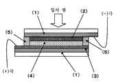
도 1은 본 발명의 단일 구조의 태양 전지(A)의 구조 형태를 나타내는 개략도.BRIEF DESCRIPTION OF THE DRAWINGS The schematic diagram which shows the structural form of the solar cell (A) of single structure of this invention.
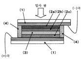
도 2는 본 발명의 탠덤(tandem) 구조의 태양 전지(B)의 구조 형태를 나타내는 개략도.2 is a schematic view showing the structural form of a tandem solar cell B of the present invention.
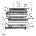
도 3은 본 발명의 탠덤 구조의 태양 전지(C)의 구조 형태를 나타내는 개략도.3 is a schematic view showing the structural form of a tandem structure solar cell (C) of the present invention.
도 4는 본 발명의 탠덤 구조의 태양 전지(D)의 구조 형태를 나타내는 개략도.4 is a schematic view showing the structural form of a solar cell (D) having a tandem structure of the present invention.
도 5는 본 발명의 탠덤 구조의 태양 전지(E)의 구조 형태를 나타내는 개략도.5 is a schematic view showing the structural form of a tandem solar cell E of the present invention.
도 6은 본 발명의 탠덤 구조의 태양 전지(F)의 구조 형태를 나타내는 개략도.Fig. 6 is a schematic diagram showing the structural form of a solar cell F having a tandem structure of the present invention.
도 7은 본 발명의 탠덤 구조의 태양 전지(G)의 구조 형태를 나타내는 개략도.7 is a schematic view showing the structural form of a solar cell G having a tandem structure according to the present invention.
도 8은 본 발명의 탠덤 구조의 태양 전지(H)의 구조 형태를 나타내는 개략 도.8 is a schematic view showing the structural form of a solar cell H having a tandem structure according to the present invention.
도 9는 본 발명의 탠덤 구조의 태양 전지(I)의 구조 형태를 나타내는 개략도.9 is a schematic view showing the structural form of the solar cell I of the tandem structure of the present invention.
이하 실시예에 근거하여, 본 발명을 더욱 상세하게 설명하지만, 본 발명이 이들 실시예에 한정되는 것은 아니다. 실시예 중, "부(部)"는 특히 지정하지 않는 한 "질량부"를 나타낸다.Based on the following Examples, although this invention is demonstrated in detail, this invention is not limited to these Examples. In the examples, "part" refers to "parts by mass" unless otherwise specified.
최대 흡수 파장은 UV-3150 스펙트로포토미터(시마즈 제작소(島津製作所)제)에 의해, 핵자기(核磁氣) 공명은 제미니(Gemini) 300(바리안(Varian)사제)에 의해 각각 측정하였다.The maximum absorption wavelength was measured by UV-3150 spectrophotometer (manufactured by Shimadzu Corporation) and nuclear magnetic resonance by Gemini 300 (manufactured by Varian).
실시예에 사용한 CMY-003, CMO-007 및 N719의 구조식을 이하에 나타낸다.The structural formulas of CMY-003, CMO-007 and N719 used in the examples are shown below.
N719는 시판품으로서 시장에서 구입하는 것이 가능하다. 또한 CMY-003 및 CMO-007은 WO2002/011213호의 실시예 1을 따라 합성하였다.N719 can be purchased in the market as a commercial item. CMY-003 and CMO-007 were also synthesized according to Example 1 of WO2002 / 011213.
에탄올 중에 있어서의 상기의 색소의 최대 흡수 파장은 아래와 같다.The maximum absorption wavelength of the said pigment in ethanol is as follows.
[화학식 1][Formula 1]

(실시예 1)(Example 1)
티타늄 이소프로폭시드(25g)와 아세트산 마그네슘 4수화물(2.5g)을, 1,4-부탄디올(130ml) 중에 현탁(懸濁)하고, 용량 300ml의 오토클레이브(autoclave) 내에 넣어서 밀봉하였다. 오토클레이브 내를 질소로 치환한 후, 300℃로 승온해서 가열하였다. 2시간 후, 300℃로 유지한 채 오토클레이브의 밸브를 열어, 용매를 제거함으로써, 크세로겔(xerogel)로서 산화 티타늄과 마그네슘의 산화물 반도체로 이루어지는 반도체 미립자 7.Og을 얻었다.Titanium isopropoxide (25 g) and magnesium acetate tetrahydrate (2.5 g) were suspended in 1,4-butanediol (130 ml) and sealed in an autoclave with a volume of 300 ml. After replacing the inside of an autoclave with nitrogen, it heated up at 300 degreeC and heated. After 2 hours, the autoclave valve was opened while maintaining the temperature at 300 ° C. to obtain 7.Og of semiconductor fine particles composed of an oxide semiconductor of titanium oxide and magnesium as xerogel.
(실시예 2∼실시예 9)(Examples 2 to 9)
실시예 1과 마찬가지의 조작에 의해, 각종의 산화물 반도체 미립자를 얻었다. 실시예 1을 포함하여, 그 결과를 정리해서 표 1에 나타낸다. 표 1 중, 「다른 쪽의 재료」라는 것은, 실시예 1에 있어서의 아세트산 마그네슘 4수화물에 상당하는 재료를 나타낸다.By the same operation as in Example 1, various oxide semiconductor fine particles were obtained. Including Example 1, the result is put together in Table 1 and shown. In Table 1, "the other material" shows the material corresponded to magnesium acetate tetrahydrate in Example 1.
[표 1][Table 1]
이소프로폭시드titanium
Isopropoxide
(g)Yield
(g)
태양 전지의 도전성 지지체인 도전성 유리 지지체(유리 기판)의 도전성 물질 FTO 상에, 실시예 1로부터 실시예 9에서 얻은 각각의 반도체 미립자를 테르피네올로 페이스트상으로 한 것을 도포하고, 450℃, 30분 소성하여, 다공질 기판을 얻었다. 또한 같은 방법에 의해, 산화 티타늄 및 산화 아연을 단독으로 사용하여, 다공질 기판을 작성하였다.On the conductive material FTO of the conductive glass support (glass substrate) which is the conductive support of the solar cell, the semiconductor fine particles obtained in Example 1 to Example 9 were coated with terpineol paste, and 450 ° C and 30 degrees. The powder was fired to obtain a porous substrate. In addition, by the same method, a porous substrate was produced using titanium oxide and zinc oxide alone.
이어서 상기의 CMY-003, CMO-007 및 N719의 색소를 각각 3.2×10⁻⁴M이 되도록 에탄올(EtOH)에 용해하고, 이 용액 중에 상기한 바와 같이 해서 얻은 다공질 기판(투명 도전성 유리 전극 위에 다공질 산화 티타늄을 450℃에서 30분 소결한 반도 체의 박막)을 실온(20℃)에서 12시간 침지해 각각의 색소를 담지시키고, 용제(에탄올)로 세정, 건조시켜서, 색소 증감된 반도체 미립자의 박막으로 이루어지는 광전 변환 소자를 얻었다.Subsequently, the above-mentioned dyes of CMY-003, CMO-007 and N719 were dissolved in ethanol (EtOH) so as to be 3.2 x 10⁻⁴ M, respectively, and the porous substrate obtained as described above in this solution (porous on the transparent conductive glass electrode). Thin film of semiconductor fine particles sintered at 450 ° C. for 30 minutes at 450 ° C.) to be immersed at room temperature (20 ° C.) for 12 hours to carry out respective dyes, washed and dried with a solvent (ethanol), and then dye-sensitized thin film of semiconductor fine particles The photoelectric conversion element which consists of was obtained.
이렇게 하여 얻은 색소 증감 반도체 미립자의 박막을 형성한 기판 상에 반도체 미립자의 박막과, 백금으로 스퍼터 된 도전성 유리의 스퍼터 면을 대치시켜서 20마이크로미터(micrometer)의 공극(空隙)을 설치해서 고정하고, 그 공극에 전해질을 함유하는 용액(전해액)을 주입하여, 공극을 채웠다. 전해액으로서, 전해액 A로서는, 3-메톡시프로피오니트릴에 요오드/요오드화 리튬/1,2-디메틸-3-n-프로필이미다졸륨 요오드/t-부틸피리딘을 각각 0.1M/0.1M/0.6M/1M이 되도록 용해한 것을 사용하고, 전해액 B로서는, 요오드/요오드화 테트라-n-프로필암모늄을 각각 0.05M/0.5M이 되도록 에틸렌 카보네이트/아세토니트릴(4/6) 중에서 조정하였다.On the substrate on which the thin film of dye-sensitized semiconductor fine particles thus obtained was formed, a thin film of semiconductor fine particles and a sputtered surface of conductive glass sputtered with platinum were replaced to form a 20 micrometer gap to fix it. A solution (electrolyte solution) containing an electrolyte was injected into the void to fill the void. As the electrolyte solution, as the electrolyte solution A, 0.1M / 0.1M / 0.6M of 3-methoxypropionitrile was respectively substituted with iodine / lithium iodide / 1,2-dimethyl-3-n-propylimidazolium iodine / t-butylpyridine. The electrolyte melted so that it became / 1M was used, and electrolyte solution B was adjusted in ethylene carbonate / acetonitrile (4/6) so that iodine / tetra- n-propyl ammonium iodide might be 0.05 M / 0.5 M, respectively.
이상과 같이 해서 얻은 본 발명의 태양 전지를 구성하는, 각각의 광전 변환 소자를 이용한 각각의 태양 전지에 대해, 이하에 나타내는 조건으로 전지 성능을 시험하였다.The battery performance was tested on the conditions shown below about each solar cell which used each photoelectric conversion element which comprises the solar cell of this invention obtained as mentioned above.
측정하는 전지의 크기는 실효(實效) 부분을 0.25cm2로 하였다. 광원(光源)은 500W 크세논 램프(xenon lamp)를 이용하고, AM(대기권 통과 공기량) 1.5필터를 통과시켜서 100mW/cm2로 하였다. 단락(短絡) 전류, 개방 전압, 변환 효율은 솔라 시뮬레이터(Solar Simulator) WXS-155S-10, AM l.5 G ((주)와콤 전창(電創) 제)를 이용해서 측정하였다.The size of the battery to be measured was 0.25 cm2 as the effective part. The light source used the 500 W xenon lamp, and let it pass the AM (atmosphere air volume) 1.5 filter, and set it as 100 mW / cm <2> . Short circuit current, open circuit voltage, and conversion efficiency were measured using the Solar Simulator WXS-155S-10, AM1.5G (made by Wacom Electric).
측정 결과를 표 2∼표 4에 나타낸다. 표 2는 N719, 표 3은 CMY-003, 표 4는 CMO-007의 색소를 이용한 전지의 시험 결과이다. 또한, 각각의 표 중에 기재한 기판 번호 1∼9는, 상기의 실시예 1∼실시예 9에서 조제한 각종의 산화물 반도체 미립자를 이용해서 작성한 다공질 기판을 이용한 것을 각각 나타내고, 또한 기판 번호 10 및 11은, 마찬가지로 작성한 산화 티타늄 및 산화 아연의 다공질 기판을 이용한 것을 각각 나타낸다.The measurement results are shown in Tables 2 to 4. Table 2 shows N719, Table 3 shows CMY-003, and Table 4 shows the test results of a battery using a dye of CMO-007. In addition, the board numbers 1-9 shown in each table show the thing using the porous board | substrate created using the various oxide semiconductor microparticles prepared in said Example 1-9, respectively, Moreover, board | substrate numbers 10 and 11 are shown, respectively. The thing using the porous board | substrate of similarly prepared titanium oxide and zinc oxide is shown, respectively.
[표 2][Table 2]
Jsc(mA/㎠)Short circuit current
Jsc (mA / ㎠)
Voc(V)Opening voltage
Voc (V)
ffShape factor
ff
η(%)Conversion efficiency
侶 (%)
2
3
4
5
6
7
8
9
10
11One
2
3
4
5
6
7
8
9
10
11
7.79
1.51
9.44
2.77
0.97
0.52
0.07
0.03
6.45
3.287.78
7.79
1.51
9.44
2.77
0.97
0.52
0.07
0.03
6.45
3.28
0.75
0.65
0.69
0.72
0.67
0.72
0.60
0.55
0.67
0.580.75
0.75
0.65
0.69
0.72
0.67
0.72
0.60
0.55
0.67
0.58
0.75
0.77
0.62
0.74
0.65
0.77
0.24
0.00
0.72
0.400.74
0.75
0.77
0.62
0.74
0.65
0.77
0.24
0.00
0.72
0.40
4.4
0.8
4.1
1.5
0.4
0.3
0.0
0.0
3.1
0.84.4
4.4
0.8
4.1
1.5
0.4
0.3
0.0
0.0
3.1
0.8
표 2의 결과로부터 명확한 바와 같이, 중파장 영역에서 최대 흡수 파장을 갖는 N719의 경우, 기판 번호 1∼2와 같이, 금속 종으로서는 티타늄과 마그네슘으로 형성한 반도체와의 매칭(matching)이 가장 우수하고, 개방 전압 및 광전 변환 효율이 가장 높은 것이 판명되었다. 중파장 영역에서 최대 흡수 파장을 갖는 색소의 경우, 보통은 산화 티타늄과의 매칭이 우수하지만, N719는 비교적 넓은 흡수 파장을 갖는다는 특성으로부터, 산화 티타늄을 단독으로 사용하는 반도체보다도 상기의 금 속 종의 조합 쪽이 더욱 높은 성능을 나타내는 것으로 생각된다. 이렇게 최대 흡수 파장이 중파장 영역에 존재하는 색소이어도, 넓은 흡수를 나타낼 경우에는 반드시 산화 티타늄이 최적인 것은 아니고, 반도체의 재질 등은 적당히 검토할 필요가 있다.As is clear from the results of Table 2, in the case of N719 having the maximum absorption wavelength in the medium wavelength region, as in the
또한, 동일한 금속 종을 이용하였을 경우라도 기판 번호 1, 2에 대한 3과의 비교로부터, 2종류의 금속 종을 혼합하는 적합한 비율이 존재하는 것이 판명되었다.Further, even when the same metal species were used, it was found from the comparison with 3 to the
이것들은 중파장 영역용의 전지로서 본 발명의 태양 전지에 사용할 수 있다. [표 3]These can be used for the solar cell of the present invention as a battery for the medium wavelength region. [Table 3]
Jsc(mA/㎠)Short circuit current
Jsc (mA / ㎠)
Voc(V)Opening voltage
Voc (V)
ffShape factor
ff
η(%)Conversion efficiency
侶 (%)
2
3
4
5
6
7
8
9
10
11One
2
3
4
5
6
7
8
9
10
11
2.47
1.27
6.19
3.37
1.29
0.48
0.08
0.05
2.41
3.253.11
2.47
1.27
6.19
3.37
1.29
0.48
0.08
0.05
2.41
3.25
0.92
0.78
0.77
0.79
0.75
0.76
0.52
0.48
0.73
0.570.91
0.92
0.78
0.77
0.79
0.75
0.76
0.52
0.48
0.73
0.57
0.80
0.83
0.77
0.74
0.76
0.74
0.48
0.42
0.70
0.620.75
0.80
0.83
0.77
0.74
0.76
0.74
0.48
0.42
0.70
0.62
1.8
0.8
3.7
2.0
0.7
0.3
0.0
0.0
1.2
1.22.1
1.8
0.8
3.7
2.0
0.7
0.3
0.0
0.0
1.2
1.2
표 3의 결과로부터 명확한 바와 같이, 단파장 영역에서 최대 흡수 파장을 갖는 CMY-003의 경우, 기판 번호 1, 2, 4 및 5와 같이, 금속 종으로서는 티타늄과 마그네슘 혹은 티타늄과 칼슘으로 형성한 반도체와의 매칭이 가장 우수하고, 개방 전압 및 광전 변환 효율이 높은 것이 판명되었다.As is clear from the results of Table 3, in the case of CMY-003 having the maximum absorption wavelength in the short wavelength region, as the
그러나 동일한 금속 종을 이용하였을 경우라도 기판 번호 1, 2에 대한 3, 혹은 기판 번호 4, 5에 대한 6과의 비교로부터, 역시 2종류의 금속 종을 혼합하는 적합한 비율이 존재하는 것이 판명되었다.However, even when the same metal species were used, a comparison with 3 for the
이것들은 단파장 영역용의 전지로서 본 발명의 태양 전지에 사용할 수 있다.These can be used for the solar cell of this invention as a battery for a short wavelength region.
[표 4][Table 4]
Jsc(mA/㎠)Short circuit current
Jsc (mA / ㎠)
Voc(V)Opening voltage
Voc (V)
ffShape factor
ff
η(%)Conversion efficiency
侶 (%)
2
3
4
5
6
7
8
9
10
11One
2
3
4
5
6
7
8
9
10
11
4.09
1.29
7.03
3.73
0.95
0.56
0.03
0.02
3.02
7.874.51
4.09
1.29
7.03
3.73
0.95
0.56
0.03
0.02
3.02
7.87
0.90
0.76
0.83
0.83
0.75
0.91
0.44
0.47
0.75
0.560.89
0.90
0.76
0.83
0.83
0.75
0.91
0.44
0.47
0.75
0.56
0.79
0.81
0.73
0.76
0.79
0.84
0.00
0.00
0.70
0.450.76
0.79
0.81
0.73
0.76
0.79
0.84
0.00
0.00
0.70
0.45
2.9
0.8
4.4
2.4
0.6
0.4
0.0
0.0
1.6
0.23.1
2.9
0.8
4.4
2.4
0.6
0.4
0.0
0.0
1.6
0.2
표 4의 결과로부터 명확한 바와 같이, CMY-003과 마찬가지로 단파장 영역에서 최대 흡수 파장을 갖는 CMO-007의 경우에도, 기판 번호 1, 2, 4 및 5와 같이, 금속 종으로서는 티타늄과 마그네슘 혹은 티타늄과 칼슘으로 형성한 반도체와의 매칭이 가장 우수하고, 개방 전압 및 광전 변환 효율이 높은 것이 판명되었다.As is clear from the results of Table 4, in the case of CMO-007 having the maximum absorption wavelength in the short wavelength region as in CMY-003, as the
또한, 동일한 금속 종을 이용하였을 경우라도 기판 번호 1, 2에 대한 3, 혹은 기판 번호 4, 5에 대한 6과의 비교로부터, 역시 2종류의 금속 종을 혼합하는 적합한 비율이 존재하는 것이 판명되었다.In addition, even when the same metal species were used, it was found from the comparison with 3 to
한편, 개방 전압에 착안하였을 경우, 기판 번호 7의 티타늄과 지르코늄으로 형성한 반도체를 이용하였을 경우가 가장 최고치를 나타내고, 이것은 CMY-003에는 보여지지 않은 특징이다.On the other hand, when attention is paid to the open circuit voltage, a semiconductor formed of titanium and zirconium of substrate number 7 is used, which is the highest value, which is a characteristic not shown in CMY-003.
이것들은 단파장 영역용의 전지로서 본 발명의 태양 전지에 사용할 수 있다.These can be used for the solar cell of this invention as a battery for a short wavelength region.
단파장 영역의 광(光)은 고에너지이기 때문에, 이 영역의 광을 효율적으로 이용할 수 있으면 결과로서 높은 전압을 나타내는 태양 전지를 얻을 수 있다. 따라서, 단파장 영역에서 전압을, 다른 파장 영역, 예를 들면 중파장 영역에서 전압과 전류를, 또한 종래 이용하는 것이 곤란하였던 장파장 영역에서 전류를 각각 얻음으로써, 폭넓은 파장 영역에서 효율적으로 에너지를 획득하는 것이 가능하게 된다.Since light in the short wavelength region is high energy, a solar cell exhibiting a high voltage as a result can be obtained as long as the light in this region can be efficiently used. Therefore, by efficiently obtaining energy in a wide wavelength region by obtaining a voltage in a short wavelength region, a voltage and a current in another wavelength region, for example, a medium wavelength region, and a current in a long wavelength region, which has conventionally been difficult to use. It becomes possible.
상기의 중파장 영역용, 단파장 영역용의 태양 전지, 및 장파장 영역용의 태양 전지를 조합함으로써, 본 발명의 태양 전지를 작성할 수 있다. 조합하는 방법에는 직렬, 병렬, 직병렬 등의 통상적인 접속 방법 등을 이용할 수 있다.The solar cell of the present invention can be prepared by combining the solar cell for the medium wavelength region, the solar cell for the short wavelength region, and the solar cell for the long wavelength region. As a combination method, the conventional connection methods, such as serial, parallel, and a parallel, can be used.
동일한 면적을 갖는 각 파장 영역용의 전지를 복수 병용할 경우에는, 광의 입사 면 측으로부터 단파장 영역용, 중파장 영역용, 또한 장파장 영역용으로 하도록, 입사 면에 가까운 측으로부터 고에너지의 광을 순차 흡수하는 구성으로 하는 것이 좋으며, 이것에 의해 본 발명의 태양 전지는 종래의 것보다 넓은 파장 영역의 광을 효율적으로 이용할 수 있다.When a plurality of batteries for each wavelength region having the same area are used in combination, light of high energy is sequentially obtained from the side close to the incident surface so as to be used for the short wavelength region, the medium wavelength region, and the long wavelength region from the incident surface side of the light. It is good to set it as the structure which absorbs, and by this, the solar cell of this invention can utilize the light of a wider wavelength range more efficiently than the conventional thing.
이하에 탠덤형 태양 전지의 작성법과 그 전지 성능의 평가 결과를 순차적으로 기재한다. 탠덤형으로 하였을 경우, 단파장 영역, 중파장 영역 및 장파장 영역용의 광전 변환 소자, 또는 그 광전 변환 소자를 갖는 태양 전지를 조합해서 전지가 형성된다. 따라서, 한쪽 전극으로서 백금으로 스퍼터 된 도전성 유리를 이용하였을 경우, 여기에서 광의 투과가 억지되고, 그 이후는 광을 투과시키는 것이 곤란하게 된다. 그러므로 탠덤형 태양 전지의 경우에는, 백금으로 스퍼터 된 도전성 유리를 이용하는 대신에, 백금 메시(mesh) 또는 백금으로 스퍼터 된 카본 메시를 사용하는 것이 바람직하다.Below, the preparation method of a tandem solar cell and the evaluation result of the battery performance are described sequentially. In the case of the tandem type, a battery is formed by combining photoelectric conversion elements for short wavelength region, medium wavelength region and long wavelength region, or solar cells having the photoelectric conversion elements. Therefore, when conductive glass sputtered with platinum is used as one electrode, light transmission is inhibited here, and after that, it becomes difficult to transmit light. Therefore, in the case of tandem solar cells, instead of using conductive glass sputtered with platinum, it is preferable to use platinum mesh or carbon mesh sputtered with platinum.
(실시예 12)(Example 12)
탠덤형 태양 전지(2셀형)의 작성Making of tandem type solar cell (2-cell type)
백금 메시의 한쪽 면(제1의 면)에, 20마이크로미터의 공극을 설치하고, 상기한 바와 같이 해서 얻은 기판 번호 1∼11의 다공질 기판에, 색소로서 CMY-003 또는 CMO-007을 담지한 광전 변환 소자의 반도체 미립자 박막을 대치시켜서 고정하였다. 마찬가지로, 메시의 다른 쪽 면(제2의 면)에, 20마이크로미터의 공극을 설치하고, 상기한 바와 같이 해서 얻은 기판 번호 10의 다공질 기판에, 색소로서 N719를 담지한 광전 변환 소자의 반도체 미립자 박막을 대치시켜서 고정하였다.20 micrometers of voids were provided on one surface (first surface) of the platinum mesh, and CMY-003 or CMO-007 was supported as a dye on the porous substrates of the boards Nos. 1 to 11 obtained as described above. The semiconductor fine particle thin film of the photoelectric conversion element was replaced and fixed. Similarly, the semiconductor fine particles of the photoelectric conversion element in which N719 is supported as a dye on a porous substrate of substrate number 10 obtained by providing a 20 micrometer gap on the other side of the mesh (second surface). The thin film was replaced and fixed.
상기 각각의 공극에 전해질을 함유하는 용액(전해액)을 주입하여, 공극을 채웠다. 전해액으로서는, 3-메톡시프로피오니트릴에 요오드/요오드화 리튬/1,2-디메틸-3-n-프로필이미다졸륨 요오드/t-부틸 피리딘을 각각 0.1M/0.1M/0.6M/1M이 되도록 용해한 것을 사용하였다.A solution (electrolyte) containing an electrolyte was injected into each of the pores to fill the pores. As an electrolyte solution, 3-methoxypropionitrile was made to be 0.1M / 0.1M / 0.6M / 1M of iodine / lithium iodide / 1,2-dimethyl-3-n-propylimidazolium iodine / t-butyl pyridine, respectively. The dissolved one was used.
이상과 같이 해서 얻은 본 발명의 탠덤형 태양 전지의 전지 성능을 상기와 같은 시험 방법에 의해 시험하였다.The battery performance of the tandem solar cell of the present invention obtained as described above was tested by the above test method.
결과를 표 5에 나타낸다.The results are shown in Table 5.
(실시예 13)(Example 13)
탠덤형 태양 전지(3셀형)의 작성Creation of tandem type solar cell (3-cell type)
이하에 3셀형의 탠덤형 태양 전지의 작성법을 기재한다. 장파장 영역에서 최대 흡수 파장을 갖는 색소로서는, 하기 식 (2)로 나타내지는 NKC-001을 이용하였다. 디클로로에탄 중에 있어서의, NKC-001의 최대 흡수 파장은 1060nm이었다.The preparation method of a 3-cell tandem solar cell is described below. As a pigment | dye which has a maximum absorption wavelength in a long wavelength region, NKC-001 represented by following formula (2) was used. The maximum absorption wavelength of NKC-001 in dichloroethane was 1060 nm.
[화학식 2](2)

(1). 태양 전지의 도전성 지지체인 도전성 유리 지지체(유리 기판)의 도전성 물질 FTO 상의 한쪽 면에 산화 티타늄을, 다른 쪽 면에 산화 주석을 각각 테르피네올로 페이스트상으로 한 것을 도포하고, 450℃, 30분 소성하여, 1장의 도전성 유리 지지체(유리 기판)의 양면에 반도체 미립자의 박막을 갖는 다공질 기판을 얻었다. 얻은 다공질 기판의 기판 번호를 기판 번호 12로 한다.(One). Titanium oxide was applied to one surface on the conductive material FTO of the conductive glass support (glass substrate) which is the conductive support of the solar cell, and tin oxide was applied to the other surface by terpineol, respectively, at 450 ° C. for 30 minutes. It baked and the porous board | substrate which has a thin film of semiconductor fine particles on both surfaces of one electroconductive glass support body (glass substrate) was obtained. The board | substrate number of the obtained porous board | substrate is set to board | substrate number 12.
(2). 이어서, 색소 N719를 3.2×10⁻⁴M이 되도록 에탄올(EtOH)에 용해하고, 이 용액 중에 상기한 바와 같이 해서 얻은 기판 번호 12의 산화 티타늄의 면만을 실온(20℃)에서 12시간 침지해 색소를 담지시켜, 용제(에탄올)로 세정하여, 건조하 였다.(2). Subsequently, the dye N719 was dissolved in ethanol (EtOH) so as to be 3.2 x 10⁻⁴ M, and only the surface of the titanium oxide of the substrate No. 12 obtained as described above in this solution was immersed at room temperature (20 ° C) for 12 hours. Was washed with a solvent (ethanol) and dried.
또한 상기 식 (2)로 나타내지는 색소인 NKC-001을 3.2×10⁻⁴M이 되도록 에탄올(EtOH)에 용해하고, 이 용액 중에 상기한 바와 같이 해서 얻은 기판 번호 12의 산화 주석의 면만을 실온(20℃)에서 12시간 침지해 색소를 담지시켜, 용제(에탄올)로 세정하여, 건조시킴으로써, 1장의 도전성 유리 지지체(유리 기판)의 양면이 색소 증감된 반도체 미립자의 박막으로 이루어지는 광전 변환 소자를 얻었다.In addition, NKC-001, which is the dye represented by the above formula (2), was dissolved in ethanol (EtOH) so as to be 3.2 x 10⁻⁴ M, and only the surface of the tin oxide of the substrate number 12 obtained as described above in this solution was room temperature. The photoelectric conversion element which consists of a thin film of semiconductor microparticles | fine-particles in which both surfaces of one electroconductive glass support body (glass substrate) was dye-sensitized by immersing at 20 degreeC for 12 hours, carrying a pigment | dye, wash | cleaning with a solvent (ethanol), and drying it Got it.
(3). 백금 메시의 한쪽 면(제1의 면)에, 20마이크로미터의 공극을 설치하고, 상기한 바와 같이 해서 얻은 기판 번호 1∼11의 각 기판을 이용해서 작성한 광전 변환 소자의 반도체 미립자 박막을 대치시켜서 고정하였다. 마찬가지로, 메시의 다른 쪽 면(제2의 면)에, 20마이크로미터의 공극을 설치하고, 상기한 바와 같이 해서 얻은 기판 번호 12의 기판을 이용해서 작성한 광전 변환 소자의 산화 티타늄의 반도체 미립자의 박막을 갖는 측의 면을 대치시켜서 고정하였다.(3). A 20 micrometer gap is provided on one surface (first surface) of the platinum mesh, and the semiconductor fine particle thin film of the photoelectric conversion element created using each of the
또한 기판 번호 12의 다른 쪽 면, 즉 산화 주석의 반도체 미립자의 박막을 갖는 면에 대하여, 20마이크로미터의 공극을 설치하고, 백금으로 스퍼터 된 도전성 유리의 스퍼터 면을 대치시켜서 고정하였다.Moreover, the space | gap of 20 micrometers was provided to the other surface of the board | substrate No. 12, ie, the surface which has a thin film of semiconductor fine particles of tin oxide, and it fixed by replacing the sputter surface of the electroconductive glass sputtered with platinum.
상기 각각의 공극에 전해질을 함유하는 용액(전해액)을 주입하여, 공극을 채웠다. 전해액으로서는, 3-메톡시프로피오니트릴에 요오드/요오드화 리튬/1,2-디메틸-3-n-프로필이미다졸륨 요오드/t-부틸 피리딘을 각각 0.1M/0.1M/0.6M/1M이 되도록 용해한 것을 사용하였다.A solution (electrolyte) containing an electrolyte was injected into each of the pores to fill the pores. As an electrolyte solution, 3-methoxypropionitrile was made to be 0.1M / 0.1M / 0.6M / 1M of iodine / lithium iodide / 1,2-dimethyl-3-n-propylimidazolium iodine / t-butyl pyridine, respectively. The dissolved one was used.
이상과 같이 해서 얻은 본 발명의 탠덤형 태양 전지(3셀형)의 전지 성능을 상기와 같은 시험 방법에 의해 시험하였다.The battery performance of the tandem solar cell (3-cell type) of the present invention obtained as described above was tested by the above test method.
결과를 표 5에 나타낸다.The results are shown in Table 5.
[표 5][Table 5]
엔트리(entry)
Entry
색소 a
Pigmented a
기판 2A
(기판 번호)
Board 2A
(Substrate number)
변환 효율
η(%)(2-cell type)
Conversion efficiency
侶 (%)
변환 효율
η(%)(3-cell type)
Conversion efficiency
侶 (%)
표 5 중, 탠덤형 태양 전지「(2셀형)」은, 「기판 2A」로서 나타낸 상기의 기판 번호 1∼11의 다공질 기판에 색소 a를 담지시켜서 작성한 광전 변환 소자와, 기판 번호 10의 다공질 기판에 색소로서 N719를 담지시켜서 작성한 광전 변환 소자를 각각 조합해서 작성한 것이다.In Table 5, a tandem solar cell "(2-cell type)" includes a photoelectric conversion element prepared by supporting a dye a on a porous substrate of the
또한 탠덤형 태양 전지「(3셀형)」은, 마찬가지로 「기판 2A」로서 나타낸 광전 변환 소자와, 상기의 기판 번호 12의 다공질 기판의 산화 티타늄의 면에 N719를, 산화 주석의 면에 NKC-001을 각각 담지시켜서 작성한 광전 변환 소자를 각각 조합해서 작성한 것이다.The tandem solar cell "(3-cell type)" is similarly referred to as "substrate 2A" and N719 on the surface of titanium oxide of the porous substrate of substrate No. 12 described above, and NKC-001 on the surface of tin oxide. It is created by combining the photoelectric conversion elements prepared by supporting each of them.
표 5 중, 기판 2A라는 것은, 산화물 반도체 미립자 박막을 갖는 도전성 유리 지지체(기판), 즉 상기의 「제1의 면」에 사용한 기판을 나타낸다. 또한 기판 2A에 있어서의 기판 번호는, 상기와 같은 의미를 갖는다.In Table 5, the board | substrate 2A shows the electroconductive glass support body (substrate) which has an oxide semiconductor fine particle thin film, ie, the board | substrate used for said "1st surface". In addition, the board | substrate number in the board | substrate 2A has the same meaning as the above.
색소 a는 산화물 반도체 미립자 박막에 담지된 색소를 의미한다.The pigment | dye a means the pigment | dye supported by the oxide semiconductor fine particle thin film.
기판 2A 중, 기판 번호 7의 기판은, 상기와 같이 실시예 번호 7에서 조제한 산화물 반도체 미립자를 이용해서 작성한 것이며, 그 산화물 반도체 미립자 중에 함유되는 각각의 금속의 비율은, 각각의 금속 원자의 질량 비율로 환산하였을 경우, 대체로 티타늄/지르코늄 = 2.4/1이다. 마찬가지로 기판 번호 8의 기판은 티타늄/지르코늄 = 1.2/1이다.In the board | substrate 2A, the board | substrate of board | substrate No. 7 was created using the oxide semiconductor microparticles prepared in Example number 7 as mentioned above, and the ratio of each metal contained in the oxide semiconductor microparticles is the mass ratio of each metal atom. In terms of, it is generally titanium / zirconium = 2.4 / 1. Likewise, the substrate of substrate number 8 is titanium / zirconium = 1.2 / 1.
표 5의 결과로부터 명확한 바와 같이, 탠덤형 태양 전지(2셀형)의 변환 효율 η는, 상당하는 단독의 전지 각각의 변환 효율보다 분명히 높은 값을 나타내고, 탠덤형으로 함으로써 단위 면적당의 광전 변환 효율을 향상시키는 것이 가능한 것이 확인되었다.As is clear from the results of Table 5, the conversion efficiency η of the tandem solar cell (2-cell type) clearly shows a higher value than the conversion efficiency of each of the corresponding single cells, and the tandem type results in the photoelectric conversion efficiency per unit area. It was confirmed that it is possible to improve.
또한, 탠덤형 태양 전지의 2셀형 및 3셀형의 각각의 변환 효율의 비교로부터, 3셀형은, 어느 경우에 있어서도 2셀형보다도 더욱 높은 변환 효율 값을 나타내고, 3셀형의 구성으로 하였을 경우에 있어서도 본 발명의 탠덤형 태양 전지는 충분한 효과를 발휘하여, 단위 면적당의 광전 변환 효율을 2셀형 이상으로 향상할 수 있는 것이 판명되었다.In addition, from the comparison of the conversion efficiency of the two-cell type and the three-cell type of the tandem solar cell, the three-cell type shows a higher conversion efficiency value than the two-cell type in any case, and the present invention is used even when the three-cell type configuration is used. It has been found that the tandem solar cell of the present invention exhibits a sufficient effect and can improve the photoelectric conversion efficiency per unit area to two or more cell types.
환언하면, 2셀형의 탠덤형 태양 전지의 변환 효율은 3.4∼6.4%인 것에 대해서, 3셀형의 탠덤형 태양 전지는 마찬가지로 3.7∼7.1%이며, 3셀형의 구조로 함으로써, 단파장 영역, 중파장 영역 및 장파장 영역의 광을 2셀형 이상으로 효율적으로 흡수하여, 광전 변환 효율을 향상시키는 효과가 있는 것이 확인되었다.In other words, while the conversion efficiency of a two-cell tandem solar cell is 3.4 to 6.4%, the three-cell tandem solar cell is similarly 3.7 to 7.1%, and the three-cell structure has a short wavelength region and a medium wavelength region. And it has been confirmed that the light of the long wavelength region is efficiently absorbed in two-cell type or more, thereby improving the photoelectric conversion efficiency.
이하에, 본 발명에 의한 태양 전지 (A)∼(I)의 작성 방법에 대해서 설명한다.EMBODIMENT OF THE INVENTION Below, the manufacturing method of the solar cell (A)-(I) by this invention is demonstrated.
태양 전지(A)Solar cell (A)
도 1(태양 전지(A))에 나타낸 바와 같이, 도전성 유리 지지체(1)의 도전성 물질 FTO 상에 산화물 반도체 미립자를 페이스트상으로 한 것을 도포하고, 450℃에서 30분 소성한 후, 색소의 3.2×10⁻⁴M 용액에 24시간 침지하여, 색소를 담지한 산화물 반도체 미립자 박막(2)을 제작하였다.As shown in FIG. 1 (solar cell (A)), the thing which made the oxide semiconductor microparticles into paste form on the electrically conductive substance FTO of the electroconductive
이어서, 동일하게 도전성 유리 지지체(1)의 도전성 물질 FTO 상에 Pt를 20Å 증착시켜서 백금 전극(3)을 제작하였다. 이것들을 밀봉재(5)로 첩합(貼合)시켜, 양극(兩極) 간의 전하 이동층(4)의 주입구(도시하지 않음)로부터 요오드계의 전하 이동층(4)을 (2)와 (3)의 사이에 충전한 후, 주입구를 밀봉재로 밀봉해서 본 발명의 태양 전지(A)를 얻었다.Subsequently, Pt was deposited by 20 kPa on the conductive material FTO of the
태양 전지(B)Solar cell (B)
도 2(태양 전지(B))에 나타낸 바와 같이, 도전성 유리 지지체(1)의 도전성 물질 FTO 상에 제1의 산화물 반도체 미립자를 페이스트상으로 한 것을 도포해서 170℃에서 30분 건조하고, 그 후에 제2의 산화물 반도체 미립자를 페이스트상으로 한 것을 도포하고, 450℃에서 30분 소성한 후, 제1의 색소의 3.2×10⁻⁴M 용액 및 제2의 색소의 3.2×10⁻⁴M 용액에 각각 24시간씩 침지하여, 제1의 색소를 담지한 제1의 산화물 반도체 미립자 박막(2a) 및 제2의 색소를 담지한 제2의 산화물 반도체 박 막(2b)을 제작하였다.As shown in FIG. 2 (solar cell B), the thing which made the 1st oxide semiconductor microparticles into paste form on the electrically-conductive substance FTO of the electroconductive
이어서, 동일하게 도전성 유리 지지체(1)의 도전성 물질 FTO 상에 Pt를 20Å 증착시켜서 백금 전극(3)을 제작하였다. 이것들을 밀봉재(5)로 첩합하고, 양극 간의 전하 이동층(4)의 주입구(도시하지 않음)로부터 요오드계의 전하 이동층(4)을 (2)와 (3)의 사이에 충전한 후, 주입구를 밀봉재로 밀봉해서 본 발명의 태양 전지(B)를 얻었다.Subsequently, Pt was deposited by 20 kPa on the conductive material FTO of the
태양 전지(C)Solar cell (C)
도 3(태양 전지(C))에 나타낸 바와 같이, 도전성 유리 지지체(1)의 도전성 물질 FTO 상에 제1의 산화물 반도체 미립자를 페이스트상으로 한 것을 도포해서 170℃에서 30분 건조하고, 그 후에 제2의 산화물 반도체 미립자를 페이스트상으로 한 것을 도포해서 170℃에서 30분 건조하고, 그 후에 제3의 산화물 반도체 미립자를 페이스트상으로 한 것을 도포하고, 450℃에서 30분 소성한 후, 제1의 색소의 3.2×10⁻⁴M 용액, 제2의 색소의 3.2×10⁻⁴M 용액 및 제3의 색소의 3.2×10⁻⁴M 용액에 각각 24시간씩 침지하여, 제1의 색소를 담지한 제1의 산화물 반도체 미립자 박막(2a), 제2의 색소를 담지한 제2의 산화물 반도체 박막(2b) 및 제3의 색소를 담지한 제3의 산화물 반도체 미립자 박막(2c)을 제작하였다.As shown in Fig. 3 (solar cell C), the first oxide semiconductor fine particles in paste form were applied onto the conductive material FTO of the
이어서, 동일하게 도전성 유리 지지체(1)의 도전성 물질 FTO 상에 Pt를 20Å 증착시켜서 백금 전극(3)을 제작하였다. 이것들을 밀봉재(5)로 첩합하고, 양극 간의 전하 이동층(4)의 주입구(도시하지 않음)로부터 요오드계의 전하 이동층(4)을 (2)와 (3)의 사이에 충전한 후, 주입구를 밀봉재로 밀봉해서 본 발명의 태양 전지(C)를 얻었다.Subsequently, Pt was deposited by 20 kPa on the conductive material FTO of the
태양 전지(D)Solar cell (D)
도 4(태양 전지(D))에 나타낸 바와 같이, 도전성 유리 지지체(1)의 도전성 물질 FTO 상에 제1의 산화물 반도체 미립자를 페이스트상으로 한 것을 도포해서 450℃에서 30분 소성한 후, 제1의 색소의 3.2×10⁻⁴M 용액에 24시간 침지하여, 제1의 색소를 담지한 제1의 산화물 반도체 박막(2a)을 제작하였다. 마찬가지로 도전성 유리 지지체(1)의 도전성 물질 FTO 상에 제2의 산화물 반도체 미립자를 페이스트상으로 한 것을 도포해서 450℃에서 30분 소성한 후, 제2의 색소의 3.2×10⁻⁴M 용액에 24시간 침지하여, 제2의 색소를 담지한 제2의 산화물 반도체 박막(2b)을 제작하였다.As shown in FIG. 4 (solar cell D), after apply | coating the thing which made the 1st oxide semiconductor microparticles into paste form on the electrically-conductive substance FTO of the electroconductive
이어서, 이것들을 백금 메시 또는 백금으로 스퍼터 된 카본 메시(3)가 사이에 오도록 대치시켜, 밀봉재(5)로 첩합하고, 전하 이동층(4)의 주입구(도시하지 않음)로부터 요오드계의 전하 이동층(4)을 (2a)와 (2b)의 사이에 충전한 후, 주입구를 밀봉재로 밀봉해서 본 발명의 태양 전지(D)를 얻었다.Subsequently, these are replaced so that a platinum mesh or the
태양 전지(E)Solar cell (E)
도 5(태양 전지(E))에 나타낸 바와 같이, 도전성 유리 지지체(1)의 도전성 물질 FTO 상에 제1의 산화물 반도체 미립자를 페이스트상으로 한 것을 도포해서 170℃에서 30분 건조하고, 그 후에 제2의 산화물 반도체 미립자를 페이스트상으로 한 것을 도포해서 450℃에서 30분 소성한 후, 제1의 색소의 3.2×10⁻⁴M 용액 및 제2의 색소의 3.2×10⁻⁴M 용액에 각각 24시간 침지하여, 제1의 색소를 담지한 제1의 산화물 반도체 박막(2a) 및 제2의 색소를 담지한 제2의 산화물 반도체 박막(2b)을 제작하였다. 마찬가지로 도전성 유리 지지체(1)의 도전성 물질 FTO 상에 제3의 산화물 반도체 미립자를 페이스트상으로 한 것을 도포해서 450℃에서 30분 소성한 후, 제3의 색소의 3.2×10⁻⁴M 용액에 24시간 침지하여, 제3의 색소를 담지한 제3의 산화물 반도체 박막(2c)을 제작하였다.As shown in FIG. 5 (solar cell E), the thing which made the 1st oxide semiconductor microparticles into paste form on the electrically-conductive substance FTO of the electroconductive
이어서, 이것들을 백금 메시 또는 백금으로 스퍼터 된 카본 메시(3)가 사이에 오도록 대치시켜, 밀봉재(5)로 첩합하고, 전하 이동층(4)의 주입구(도시하지 않음)로부터 요오드계의 전하 이동층(4)을 (2a), (2b)와 (2c)의 사이에 충전한 후, 주입구를 밀봉재로 밀봉해서 본 발명의 태양 전지(E)를 얻었다.Subsequently, these are replaced so that a platinum mesh or the
태양 전지(F)Solar cell (F)
도 6(태양 전지(F))에 나타낸 바와 같이, 도전성 유리 지지체(1)의 도전성 물질 FTO 상에 제1의 산화물 반도체 미립자를 페이스트상으로 한 것을 도포해서 170℃에서 30분 건조하고, 그 후에 제2의 산화물 반도체 미립자를 페이스트상으로 한 것을 도포해서 450℃에서 30분 소성한 후, 제1의 색소의 3.2×10⁻⁴M 용액 및 제2의 색소의 3.2×10⁻⁴M 용액에 각각 24시간 침지하여, 제1의 색소를 담지한 제1의 산화물 반도체 박막(2a) 및 제2의 색소를 담지한 제2의 산화물 반도체 박막(2b)을 제 작하였다. 마찬가지로 도전성 유리 지지체(1)의 도전성 물질 FTO 상에 제3의 산화물 반도체 미립자를 페이스트상으로 한 것을 도포해서 450℃에서 30분 소성한 후, 제3의 색소의 3.2×10⁻⁴M 용액에 24시간 침지하여, 제3의 색소를 담지한 제3의 산화물 반도체 박막(2c)을 제작하였다.As shown in FIG. 6 (solar cell F), the thing which made the 1st oxide semiconductor fine particle into paste form on the electrically-conductive substance FTO of the electroconductive
이어서, 이것들을 밀봉재(5)로 첩합하고, 양극 간의 전하 이동층(4)의 주입구(도시하지 않음)로부터 요오드계의 전하 이동층(4)을 (2a)와 (2b)의 사이에 충전한 후, 주입구를 밀봉재로 밀봉해서 본 발명의 태양 전지(F)를 얻었다.Subsequently, these are bonded together with the sealing
태양 전지(G)Solar cell (G)
도 7(태양 전지(G))에 나타낸 바와 같이, 도전성 유리 지지체(1)의 도전성 물질 FTO 상에 제1의 산화물 반도체 미립자를 페이스트상으로 한 것을 도포해서 170℃에서 30분 건조하고, 그 후에 제2의 산화물 반도체 미립자를 페이스트상으로 한 것을 도포해서 450℃에서 30분 소성한 후, 제1의 색소의 3.2×10⁻⁴M 용액 및 제2의 색소의 3.2×10⁻⁴M 용액에 각각 24시간 침지하여, 제1의 색소를 담지한 제1의 산화물 반도체 박막(2a) 및 제2의 색소를 담지한 제2의 산화물 반도체 박막(2b)을 제작하였다. 마찬가지로 도전성 유리 지지체(1)의 도전성 물질 FTO 상에 제3의 산화물 반도체 미립자를 페이스트상으로 한 것을 도포해서 450℃에서 30분 소성한 후, 제3의 색소의 3.2×10⁻⁴M 용액에 24시간 침지하여, 제3의 색소를 담지한 제3의 산화물 반도체 박막(2c)을 제작하였다.As shown in FIG. 7 (solar cell G), the thing which made the 1st oxide semiconductor microparticles into paste form on the electrically-conductive substance FTO of the electroconductive
이어서, 이것들을 밀봉재(5)로 첩합하고, 양극 간의 전하 이동층(4)의 주입구(도시하지 않음)로부터 요오드계의 전하 이동층(4)을 (2a), (2b)와 (2c)의 사이에 충전한 후, 주입구를 밀봉재로 밀봉해서 본 발명의 태양 전지(G)를 얻었다.Subsequently, these are bonded together with the sealing
태양 전지(H)Solar cell (H)
도 8(태양 전지(H))에 나타낸 바와 같이, 도전성 유리 지지체(1)의 도전성 물질 FTO 상에 제1의 산화물 반도체 미립자를 페이스트상으로 한 것을 도포하고, 450℃에서 30분 소성한 후, 제1의 색소의 3.2×10⁻⁴M 용액에 24시간 침지하여, 제1의 색소를 담지한 제1의 산화물 반도체 미립자 박막(2a)을 제작하였다. 마찬가지로, 도전성 유리 지지체(1)의 도전성 물질 FTO 상에 제2의 산화물 반도체 미립자를 페이스트상으로 한 것을 도포하고, 450℃에서 30분 소성한 후, 제2의 색소의 3.2×10⁻⁴M 용액에 24시간 침지하여, 제2의 색소를 담지한 제2의 산화물 반도체 미립자 박막(2b)을 제작하였다.As shown in FIG. 8 (solar cell H), after apply | coating the thing which made the 1st oxide semiconductor microparticles into paste form on the conductive material FTO of the electroconductive
이어서, 동일하게 도전성 유리 지지체(1)의 도전성 물질 FTO 상에 Pt를 20Å 증착시켜서 백금 전극(3)을 제작하였다. 이것들을 각각 밀봉재(5)로 첩합하고, 양극 간의 전하 이동층(4)의 주입구(도시하지 않음)로부터 요오드계의 전하 이동층(4)을 (2)와 (3)의 사이에 충전한 후, 주입구를 밀봉재로 밀봉하여, 2개의 태양 전지를 제작하였다. 이것들을 입사 광에 대하여 수직으로 배치하고, 직렬로 배선함으로써 본 발명의 태양 전지(H)를 얻었다.Subsequently, Pt was deposited by 20 kPa on the conductive material FTO of the
태양 전지(I)Solar cell (I)
도 9(태양 전지(I))에 나타낸 바와 같이, 도전성 유리 지지체(1)의 도전성 물질 FTO 상에 제1의 산화물 반도체 미립자를 페이스트상으로 한 것을 도포하고, 450℃에서 30분 소성한 후, 제1의 색소의 3.2×10⁻⁴M 용액에 24시간 침지하여, 제1의 색소를 담지한 제1의 산화물 반도체 미립자 박막(2a)을 제작하였다. 마찬가지로, 도전성 유리 지지체(1)의 도전성 물질 FTO 상에 제2의 산화물 반도체 미립자를 페이스트상으로 한 것을 도포하고, 450℃에서 30분 소성한 후, 제2의 색소의 3.2×10⁻⁴M 용액에 24시간 침지하여, 제2의 색소를 담지한 제2의 산화물 반도체 미립자 박막(2b)을 제작하였다. 마찬가지로, 도전성 유리 지지체(1)의 도전성 물질 FTO 상에 제3의 산화물 반도체 미립자를 페이스트상으로 한 것을 도포하고, 450℃에서 30분 소성한 후, 제3의 색소의 3.2×10⁻⁴M 용액에 24시간 침지하여, 제3의 색소를 담지한 제3의 산화물 반도체 미립자 박막(2c)을 제작하였다.As shown in FIG. 9 (solar cell I), after apply | coating the thing which made the 1st oxide semiconductor microparticles into paste form on the electrically-conductive substance FTO of the electroconductive
이어서, 동일하게 도전성 유리 지지체(1)의 도전성 물질 FTO 상에 Pt를 20Å 증착시켜서 백금 전극(3)을 제작하였다. 이것들을 각각 밀봉재(5)로 첩합하고, 양극 간의 전하 이동층(4)의 주입구(도시하지 않음)로부터 요오드계의 전하 이동층(4)을 (2)와 (3)의 사이에 충전한 후, 주입구를 밀봉재로 밀봉하여, 3개의 태양 전지를 제작하였다. 이것들을 입사 광에 대하여 수직으로 배치하고, 직렬로 배선함으로써 본 발명의 태양 전지(I)를 얻었다.Subsequently, Pt was deposited by 20 kPa on the conductive material FTO of the
이어서, 태양 전지 (A), (D), (H) 및 (I)에 대해서, 색소와 산화물 반도체 및 복합 산화물 반도체와의 조합 및 그것을 이용한 탠덤 셀의 광전 변환 능력(개방 전압)을 평가하였다. 결과를 하기 표 6에 나타낸다.Subsequently, the photovoltaic conversion ability (opening voltage) of the tandem cell using the combination of a pigment, an oxide semiconductor, and a composite oxide semiconductor, and the same about the solar cells (A), (D), (H), and (I) was evaluated. The results are shown in Table 6 below.
[표 6-1][Table 6-1]
[표 6-2][Table 6-2]
Example 56
D
0.74
A
Example 57
D
0.75
A
Example 58
D
0.75
B
Example 59
D
0.81
B
Example 60
D
0.79
B
Example 61
H
1.75
Example 62
H
1.68
Example 63
H
1.69
Example 64
H
1.75
실시예 65
Example 65
H
H
(2a)
(2a)
Mg(0.10)
Mg (0.10)
1.21
1.21
B
B
실시예 66
Example 66
I
I
2.05
2.05
실시예 67
Example 67
I
I
1.96
1.96
실시예 68
Example 68
I
I
2.15
2.15
실시예 69
Example 69
I
I
2.13
2.13
[표 6-3][Table 6-3]
비교예 10
Comparative Example 10
D
D
0.74
0.74
A
A
비교예 11
Comparative Example 11
D
D
0.73
0.73
A
A
비교예 12
Comparative Example 12
H
H
1.45
1.45
비교예 13
Comparative Example 13
I
I
1.81
1.81
비교예 14
Comparative Example 14
I
I
1.82
1.82
상기 표 6으로부터, 이하의 고찰이 가능하다.From the said Table 6, the following considerations are possible.
실시예 14∼실시예 55 및 비교예 1∼비교예 9에서는, 단일 구조의 태양 전지(A)에서 사용한 색소(S-1, S-2, S-3, S-4, M-7, M-3, M-4, M-5, L-1) 모두에 있어서, 산화 티타늄을 본원 복합 산화물로 함으로써 대폭적인 개방 전압(Voc)의 향상이 관측되었다. 또한, 실시예 56∼실시예 60 및 비교예 10 및 비교예 11에서는, 병렬 구조의 태양 전지(D)에 있어서, 본원 실시예에서의 개방 전압이 대폭적으로 증가(비교예 대비)하였다. 실시예 61∼실시예 65 및 비교예 12에서는, 직렬 2층 구조의 태양 전지(H)에 있어서, 본원 실시예에서의 개방 전압의 대폭적인 증가가 관측되었다. 실시예 66∼실시예 69 및 비교예 13 및 비교예 14에서는, 직렬 3층 구조의 태양 전지(I)에 있어서, 본원 실시예에서의 개방 전압의 대폭적인 증가가 관측되었다.In Examples 14 to 55 and Comparative Examples 1 to 9, the dyes (S-1, S-2, S-3, S-4, M-7, M used in the solar cell A of a single structure) In all of -3, M-4, M-5, and L-1), when titanium oxide was used as the complex oxide of the present application, a significant improvement in the open voltage Voc was observed. Further, in Examples 56 to 60, Comparative Examples 10, and 11, in the solar cell D having a parallel structure, the open circuit voltage in the example of the present application was significantly increased (compared to Comparative Example). In Examples 61 to 65 and Comparative Example 12, in the solar cell H of the series two-layer structure, a significant increase in the open voltage in the Example of the present application was observed. In Examples 66 to 69, Comparative Example 13, and Comparative Example 14, in the solar cell I having a series three-layer structure, a significant increase in the open voltage in the present Example was observed.
이와 같이, 색소마다 적합한 산화물 및 복합 산화물 반도체를 선택해 조합함으로써 높은 전압의 태양 전지를 얻는 것이 가능하다. 또한, 이것들을 더욱 포개 탠덤 구조로 함으로써, 태양 전지의 면적을 넓히는 일 없이 작은 면적으로 전압을 향상시키는 것이 가능하게 되었다. 작은 면적에서 고전압을 얻을 수 있는 태양 전지는, 휴대 전화나 탁상 전자계산기 등의 휴대 용도나, 구동에 고전압을 필요로 하는, 액정, 전기 루미네선스(electroluminescence; EL), 플라즈마 디스플레이(PDP), 전자 페이퍼(DP) 등의 각종 디스플레이 용도에 적합하며, 본원 발명의 태양 전지를 이용함으로써 이들 제품의 경량화 및 소형화를 가능하게 하는 것으로 생각된다. 또한, 리튬 이온 2차 전지, 니켈-수소 2차 전지, 커패시터, 콘덴서 등의 충전 용도에 대하여도 본원 발명의 고전압 태양 전지를 이용함으로써, 고전압 충전이 가능하게 되어, 에너지 로스(loss)가 적은 충전이 가능하게 된다.In this way, it is possible to obtain a high voltage solar cell by selecting and combining a suitable oxide and a composite oxide semiconductor for each dye. Moreover, by making these tandem structures further, it is possible to improve the voltage with a small area without increasing the area of the solar cell. Solar cells capable of obtaining high voltage in a small area include liquid crystals, electroluminescence (EL), plasma displays (PDP), which require high voltages for portable applications such as mobile phones and desktop electronic calculators, and driving. It is suitable for various display uses, such as electronic paper (DP), and is considered to enable the weight reduction and miniaturization of these products by using the solar cell of this invention. In addition, high voltage charging is possible by using the high voltage solar cell of the present invention for charging applications such as a lithium ion secondary battery, a nickel-hydrogen secondary battery, a capacitor, a capacitor, and the like, and a charge with low energy loss is possible. This becomes possible.
이어서, 태양 전지(D)에 대해서, 색소와 산화물 반도체 및 복합 산화물 반도체와의 조합 및 그것을 이용한 탠덤 셀의 광전 변환 능력(단락 전류)을 평가하였다. 결과를 하기 표 7에 나타낸다.Next, about the solar cell D, the combination of a dye, an oxide semiconductor, and a composite oxide semiconductor, and the photoelectric conversion ability (short circuit current) of the tandem cell using the same were evaluated. The results are shown in Table 7 below.
[표 7][Table 7]
예 번호
Yes No
전 지
battery
반도체층 번호
Semiconductor layer number
반도체oxide
semiconductor
색소
Pigment
Isc/mA/㎠
Isc / mA / ㎠
전해액
Electrolyte
실시예 70
Example 70
D
D
10.85
10.85
A
A
비교예 15
Comparative Example 15
D
D
9.20
9.20
A
A
상기 표 7로부터, 이하의 고찰이 가능하다.From the above Table 7, the following considerations are possible.
실시예 70과 비교예 15로부터, 병렬 구조의 태양 전지(D)에 있어서, 단파장 영역용의 반도체를 산화 티타늄 대신에 본원의 복합 산화물로 사용함으로써 단락 전류의 향상이 보인다.From Example 70 and Comparative Example 15, in the parallel solar cell D, the short-circuit current was improved by using the semiconductor for short wavelength region as the complex oxide of the present application instead of titanium oxide.
이것으로부터, 본원 발명의 태양 전지는, 단락 전류도 향상시킬 수 있고, 작은 면적에서 큰 전류를 얻는 것이 가능하게 되었다.From this, the solar cell of the present invention can also improve the short circuit current, and it is possible to obtain a large current in a small area.
상기한 바와 같이 본 발명의 탠덤형 태양 전지는, 2셀형, 또는 3셀형의 어느 구성에 있어서도 충분한 효과를 발휘하며, 태양 전지로서 우수한 것으로 판명되었다.As described above, the tandem solar cell of the present invention exhibits a sufficient effect in any two-cell or three-cell configuration, and has been found to be excellent as a solar cell.
본 실시예에 있어서는 2셀형으로서는 단파장 영역 및 중파장 영역용의 광전 변환 소자(단파장 영역 또는 중파장 영역에서 최대 흡수 파장을 갖는 색소를 담지한 다공질 기판을 이용해서 작성한 광전 변환 소자)를 조합한 탠덤형 태양 전지를 작성하였다.In this embodiment, as a two-cell type tandem in which a photoelectric conversion element for a short wavelength region and a medium wavelength region (photoelectric conversion element created using a porous substrate carrying a dye having the maximum absorption wavelength in the short wavelength region or the medium wavelength region) is combined. The type solar cell was created.
또한, 3셀형으로서는 단파장 영역, 중파장 영역 및 장파장 영역용의 광전 변환 소자(단파장 영역에서 최대 흡수 파장을 갖는 색소를 담지한 다공질 기판을 이용해서 작성한 광전 변환 소자와, 중파장 영역용 및 장파장 영역에서 최대 흡수 파장을 갖는 색소를 1장의 다공질 기판의 양면에 각각 담지한 것을 이용해서 작성한 광전 변환 소자)를 조합한 탠덤형 태양 전지를 작성하였다. 그러나, 이들 단파장 영역, 중파장 영역 및 장파장 영역용의 광전 변환 소자는, 특히 이 조합에는 한정되지 않고, 어느 조합을 이용해서 탠덤형의 태양 전지를 만드는 것도 가능하다. 본 발명에는, 이렇게 어느 조합을 이용하는 태양 전지도 포함된다.In addition, the three-cell type photoelectric conversion element for short wavelength region, medium wavelength region and long wavelength region (photoelectric conversion element prepared by using a porous substrate carrying a dye having the maximum absorption wavelength in the short wavelength region, medium wavelength region and long wavelength region). The tandem solar cell which combined the photoelectric conversion element created by using the pigment | dye which has the maximum absorption wavelength in each of the porous board | substrates of 1 sheet each was created. However, the photoelectric conversion elements for the short wavelength region, the medium wavelength region, and the long wavelength region are not particularly limited to this combination, and it is also possible to make a tandem solar cell using any combination. This invention also includes the solar cell using any combination in this way.
본원의 태양 전지에 이용한 색소를 이하에 나타낸다.The pigment | dye used for the solar cell of this application is shown below.
실시예 중, 단파장 영역용으로서 이용한 색소를 이하에 나타낸다.In the Example, the pigment | dye used for the short wavelength area | region is shown below.
[화학식 3](3)

실시예 중, 중파장 영역용으로서 이용한 색소를 이하에 나타낸다.In the Example, the pigment | dye used for the medium wavelength area | region is shown below.
[화학식 4][Formula 4]

실시예 중, 장파장 영역용으로서 이용한 색소를 이하에 나타낸다.In the Example, the pigment | dye used for the long wavelength area | region is shown below.
[화학식 5][Chemical Formula 5]

본 발명의 태양 전지는, 변환 효율, 특히 단파장 영역 및 장파장 영역에 있어서의 변환 효율이 높은 태양 전지로서, 광범위한 분야에서 효과적으로 이용된다.The solar cell of the present invention is a solar cell having high conversion efficiency, in particular, high conversion efficiency in a short wavelength region and a long wavelength region, and is effectively used in a wide range of fields.
Claims (26)
Translated fromKoreanApplications Claiming Priority (5)
| Application Number | Priority Date | Filing Date | Title |
|---|---|---|---|
| JP2006186111 | 2006-07-05 | ||
| JPJP-P-2006-186111 | 2006-07-05 | ||
| JPJP-P-2006-271939 | 2006-10-03 | ||
| JP2006271939 | 2006-10-03 | ||
| PCT/JP2007/063371WO2008004580A1 (en) | 2006-07-05 | 2007-07-04 | Dye-sensitized solar cell |
Publications (2)
| Publication Number | Publication Date |
|---|---|
| KR20090037867A KR20090037867A (en) | 2009-04-16 |
| KR101341299B1true KR101341299B1 (en) | 2013-12-12 |
Family
ID=38894547
Family Applications (1)
| Application Number | Title | Priority Date | Filing Date |
|---|---|---|---|
| KR1020087032191AExpired - Fee RelatedKR101341299B1 (en) | 2006-07-05 | 2007-07-04 | Dye-sensitized solar cell |
Country Status (9)
| Country | Link |
|---|---|
| US (1) | US20090242027A1 (en) |
| EP (1) | EP2037528A4 (en) |
| JP (1) | JP5084730B2 (en) |
| KR (1) | KR101341299B1 (en) |
| CN (1) | CN101485036B (en) |
| AU (1) | AU2007270404B2 (en) |
| CA (1) | CA2655192A1 (en) |
| TW (1) | TWI407616B (en) |
| WO (1) | WO2008004580A1 (en) |
Families Citing this family (21)
| Publication number | Priority date | Publication date | Assignee | Title |
|---|---|---|---|---|
| CN101240117B (en)* | 2008-02-04 | 2010-11-10 | 中国科学院长春应用化学研究所 | Pure organic dyestuff and dyestuff sensitization solar energy battery prepared therefrom |
| TWI384034B (en)* | 2008-04-07 | 2013-02-01 | Everlight Chem Ind Corp | Dye compound for dye-sensitized solar cell |
| WO2009133806A1 (en)* | 2008-05-02 | 2009-11-05 | ペクセル・テクノロジーズ株式会社 | Dye-sensitized photoelectric conversion element |
| EP2408057A4 (en)* | 2009-03-11 | 2013-02-20 | Nat University Corp Kyushu Inst Of Technology | COLOR-SENSITIZED SOLAR CELL |
| US8294858B2 (en)* | 2009-03-31 | 2012-10-23 | Intel Corporation | Integrated photovoltaic cell for display device |
| KR101131395B1 (en)* | 2009-05-20 | 2012-04-03 | 고려대학교 산학협력단 | Method of adsorbing dye on nanoparticle, method of manufacturing dye-sensitized solar cell using the same and dye sensitized solar cell manufactured by the same |
| EP2385556B1 (en)* | 2010-05-04 | 2021-01-20 | Heliatek GmbH | Photoactive device with organic layers |
| TWI426648B (en)* | 2010-12-13 | 2014-02-11 | Innot Bioenergy Holding Co | Organic negative electrode and battery using the organic negative electrode |
| TWI511310B (en)* | 2012-01-17 | 2015-12-01 | Microjet Technology Co Ltd | Manufacturing method of dye sensitized solar cell |
| KR20140138749A (en)* | 2012-03-30 | 2014-12-04 | 가부시키가이샤 아데카 | Dye-sensitized solar cell and method of manufacturing same |
| WO2013171520A1 (en) | 2012-05-18 | 2013-11-21 | Isis Innovation Limited | Optoelectronic device comprising perovskites |
| GB201208793D0 (en) | 2012-05-18 | 2012-07-04 | Isis Innovation | Optoelectronic device |
| US10388897B2 (en) | 2012-05-18 | 2019-08-20 | Oxford University Innovation Limited | Optoelectronic device comprising porous scaffold material and perovskites |
| KR102698732B1 (en)* | 2012-09-18 | 2024-08-27 | 옥스포드 유니버시티 이노베이션 리미티드 | Optoelectonic device |
| US9640331B2 (en) | 2013-03-22 | 2017-05-02 | Sharp Laboratories Of America, Inc. | Solid state dye-sensitized solar cell tandem module |
| TWI473780B (en) | 2014-04-09 | 2015-02-21 | Nat Univ Chung Hsing | Photosensitive dye compound and dye-sensitized solar cell |
| JP6821956B2 (en)* | 2016-06-06 | 2021-01-27 | 日本精工株式会社 | Photoelectric conversion element |
| US11017957B2 (en) | 2016-08-12 | 2021-05-25 | Sharp Kabushiki Kaisha | Dye-sensitized solar cell |
| EP3499531B1 (en)* | 2016-08-12 | 2021-02-24 | Sharp Kabushiki Kaisha | Dye-sensitized solar battery and method for producing same |
| JP6880748B2 (en)* | 2017-01-10 | 2021-06-02 | 株式会社リコー | Photoelectric conversion element and solar cell |
| FI130068B (en)* | 2018-12-31 | 2023-01-31 | Aalto Univ Foundation Sr | A double sided solar cell assembly |
Citations (3)
| Publication number | Priority date | Publication date | Assignee | Title |
|---|---|---|---|---|
| JP2002222971A (en) | 2001-01-29 | 2002-08-09 | Sharp Corp | Photoelectric conversion element |
| JP2003100359A (en) | 2001-09-25 | 2003-04-04 | Fuji Xerox Co Ltd | Functional film and manufacturing method therefor, and optical semiconductor electrode and photoelectric conversion element using the film |
| JP2003168496A (en) | 2001-12-03 | 2003-06-13 | Big Technos Kk | Photoelectric cell |
Family Cites Families (204)
| Publication number | Priority date | Publication date | Assignee | Title |
|---|---|---|---|---|
| JP2572402B2 (en) | 1987-10-23 | 1997-01-16 | 日本電信電話株式会社 | Access method for optical fiber line and connector plug thereof |
| CH674596A5 (en)* | 1988-02-12 | 1990-06-15 | Sulzer Ag | |
| JPH031273A (en) | 1989-05-29 | 1991-01-07 | Sharp Corp | Character processor having operation self-study function |
| DE69115688T2 (en) | 1990-04-17 | 1996-08-14 | Ecole Polytech | PHOTOVOLTAIC CELLS |
| GB9217811D0 (en) | 1992-08-21 | 1992-10-07 | Graetzel Michael | Organic compounds |
| WO1995029924A1 (en) | 1994-05-02 | 1995-11-09 | Ecole Polytechnique Federale De Lausanne (Epfl) | Phosphonated polypyridyl compounds and their complexes |
| JP4081149B2 (en) | 1996-01-12 | 2008-04-23 | 山本化成株式会社 | Wet solar cells using phthalocyanine compounds |
| JPH1051049A (en) | 1996-08-06 | 1998-02-20 | Tokyo Gas Co Ltd | Control method of electron transfer direction in light energy conversion system using dye and light energy conversion device using the same |
| JP2955647B2 (en) | 1996-09-12 | 1999-10-04 | 工業技術院長 | Organic dye-sensitized oxide semiconductor electrode and solar cell including the same |
| JPH1093121A (en) | 1996-09-13 | 1998-04-10 | Fuji Photo Film Co Ltd | Solar battery |
| JP3968809B2 (en) | 1996-12-19 | 2007-08-29 | 富士ゼロックス株式会社 | Photo-semiconductor electrode for wet solar cell, wet solar cell, and photoelectric conversion method |
| JP3968819B2 (en) | 1997-06-02 | 2007-08-29 | 富士ゼロックス株式会社 | Photo-semiconductor electrode for wet solar cell, wet solar cell, and photoelectric conversion method |
| JP3369439B2 (en) | 1997-06-05 | 2003-01-20 | 科学技術振興事業団 | Photoresponsive electrode and wet solar cell |
| JP4116158B2 (en) | 1997-07-15 | 2008-07-09 | 富士フイルム株式会社 | Semiconductor fine particles, photoelectric conversion element and photochemical battery |
| JP4148374B2 (en) | 1997-07-18 | 2008-09-10 | 富士フイルム株式会社 | Photoelectric conversion element and photoelectrochemical cell |
| JP4148375B2 (en) | 1997-07-18 | 2008-09-10 | 富士フイルム株式会社 | Photoelectric conversion element and photoelectrochemical cell |
| JP3286905B2 (en) | 1997-08-04 | 2002-05-27 | 株式会社リコー | Phthalocyanine compound |
| JPH1197725A (en) | 1997-09-16 | 1999-04-09 | Fuji Photo Film Co Ltd | Photoelectric conversion element and photoelectrochemical cell |
| JPH11167937A (en) | 1997-09-30 | 1999-06-22 | Fuji Photo Film Co Ltd | Photoelectric transfer element |
| JP4169220B2 (en) | 1997-11-27 | 2008-10-22 | 富士フイルム株式会社 | Photoelectric conversion element |
| JPH11204821A (en) | 1998-01-09 | 1999-07-30 | Fuji Xerox Co Ltd | Optical semiconductor electrode, photoelectric conversion device, and photoelectric conversion method |
| JPH11273753A (en) | 1998-03-25 | 1999-10-08 | Sekisui Chem Co Ltd | Coloring matter sensitizing type photocell |
| JP2997773B1 (en) | 1998-07-15 | 2000-01-11 | 工業技術院長 | Metal complexes, oxide semiconductor electrodes and solar cells useful as sensitizers |
| JP2000082506A (en) | 1998-09-08 | 2000-03-21 | Fuji Xerox Co Ltd | Photosemiconductor electrode, photoelectric conversion device and photoelectric conversion method |
| JP4024942B2 (en)* | 1998-09-16 | 2007-12-19 | 株式会社東芝 | Dye-sensitized photochemical cell |
| JP3945038B2 (en) | 1998-09-21 | 2007-07-18 | 松下電器産業株式会社 | Dye-sensitized solar cell |
| JP2000100483A (en) | 1998-09-22 | 2000-04-07 | Sharp Corp | Photoelectric conversion element, method of manufacturing the same, and solar cell using the same |
| JP2000106224A (en) | 1998-09-29 | 2000-04-11 | Fuji Photo Film Co Ltd | Photoelectric conversion element and photo electrochemical cell |
| JP4217320B2 (en) | 1998-12-24 | 2009-01-28 | 富士フイルム株式会社 | Photoelectric conversion element and photoelectrochemical cell |
| JP4460686B2 (en) | 1998-12-28 | 2010-05-12 | 富士フイルム株式会社 | Photoelectric conversion element and photoelectrochemical cell |
| JP2000223167A (en) | 1999-01-28 | 2000-08-11 | Fuji Photo Film Co Ltd | Photoelectric conversion element, and photoelectric chemical battery |
| JP2000228233A (en) | 1999-02-04 | 2000-08-15 | Fuji Photo Film Co Ltd | Pigment adsorbing semiconductor fine grain, pigment adsorbing method to semiconductor fine grain, optoelectronic transducer element and optoelectronic chemical cell |
| JP2000235874A (en) | 1999-02-15 | 2000-08-29 | Fuji Photo Film Co Ltd | Photoelectric conversion element and photo electrochemical battery |
| JP4026266B2 (en) | 1999-02-19 | 2007-12-26 | 富士ゼロックス株式会社 | Semiconductor electrode and photovoltaic cell |
| JP4211120B2 (en) | 1999-02-19 | 2009-01-21 | 富士ゼロックス株式会社 | Photo-semiconductor electrode, photoelectric conversion device, and photoelectric conversion method |
| JP2000251956A (en) | 1999-02-24 | 2000-09-14 | Toyota Central Res & Dev Lab Inc | Solar cell |
| JP2000251957A (en) | 1999-03-02 | 2000-09-14 | Fuji Photo Film Co Ltd | Optoelectric transducing element and photoelectrochemical cell |
| JP3505425B2 (en) | 1999-03-15 | 2004-03-08 | 株式会社東芝 | Photoelectric conversion element and photosensitizing dye for photoelectric conversion element |
| JP2000268889A (en) | 1999-03-15 | 2000-09-29 | Toshiba Corp | Photovoltaic device |
| JP2000277180A (en) | 1999-03-24 | 2000-10-06 | Fuji Photo Film Co Ltd | Photoelectric transfer element and photoelectrochemical battery |
| JP2000285978A (en) | 1999-03-31 | 2000-10-13 | Fuji Photo Film Co Ltd | Coloring agent, photoelectric conversion element, and photoelectrochemical battery |
| JP4392769B2 (en) | 1999-03-31 | 2010-01-06 | 富士フイルム株式会社 | Photoelectric conversion element, solar cell and solar cell module |
| JP2000294305A (en) | 1999-04-02 | 2000-10-20 | Fuji Photo Film Co Ltd | Photoelectric transducer element and optically electrochemical battery |
| JP2000294303A (en) | 1999-04-02 | 2000-10-20 | Fuji Photo Film Co Ltd | Photoelectric converting element and photoelectric chemical battery |
| JP4285671B2 (en) | 1999-06-14 | 2009-06-24 | 富士フイルム株式会社 | Photoelectric conversion device, photoelectrochemical cell, and metal complex dye |
| JP3680094B2 (en) | 1999-06-02 | 2005-08-10 | 独立行政法人産業技術総合研究所 | Organic dye-sensitized porous oxide semiconductor electrode and solar cell using the same |
| JP2001060467A (en) | 1999-06-14 | 2001-03-06 | Fuji Photo Film Co Ltd | Photoelectric converting element, photoelectrochemical battery and metallic complex pigment |
| JP4162106B2 (en) | 1999-06-17 | 2008-10-08 | 富士フイルム株式会社 | Photoelectric conversion device, photoelectrochemical cell, and metal complex dye |
| JP2001060468A (en) | 1999-06-18 | 2001-03-06 | Fuji Photo Film Co Ltd | Photoelectric converting element, photocell and metallic complex pigment |
| JP2001006761A (en) | 1999-06-18 | 2001-01-12 | Fuji Photo Film Co Ltd | Photoelectric conversion material, photoelectric conversion element, and polymethine dye |
| US6936143B1 (en) | 1999-07-05 | 2005-08-30 | Ecole Polytechnique Federale De Lausanne | Tandem cell for water cleavage by visible light |
| JP4439619B2 (en) | 1999-07-09 | 2010-03-24 | 富士フイルム株式会社 | Semiconductor fine particles, photoelectric conversion material, and photoelectric conversion element |
| JP2001043906A (en) | 1999-07-28 | 2001-02-16 | Fuji Photo Film Co Ltd | Photoelectric converting element and photoelectric chemical battery |
| JP3750011B2 (en) | 1999-07-29 | 2006-03-01 | 独立行政法人科学技術振興機構 | Method for producing metal complex and amino acid modified metal complex |
| JP2001067931A (en) | 1999-08-25 | 2001-03-16 | Fuji Photo Film Co Ltd | Electrolyte composition, photoelectric conversion element and photoelectrochemical battery |
| JP2001076773A (en) | 1999-08-31 | 2001-03-23 | Fuji Photo Film Co Ltd | Photoelectric transfer element, photoelectrochemical cell, and new squalenium cyanine dye |
| JP2001076775A (en) | 1999-09-07 | 2001-03-23 | Fuji Photo Film Co Ltd | Photoelectric transfer element and photocell |
| JP2001093589A (en) | 1999-09-21 | 2001-04-06 | Fuji Xerox Co Ltd | Optical semiconductor electrode, photoelectric conversion device and photoelectric conversion method |
| JP2001167808A (en) | 1999-12-09 | 2001-06-22 | Fuji Photo Film Co Ltd | Photoelectric conversion element and photocell |
| JP2001203005A (en) | 2000-01-21 | 2001-07-27 | Fuji Photo Film Co Ltd | Photoelectric transducer element, photo cells and metal complex dyes |
| JP4352552B2 (en) | 2000-01-21 | 2009-10-28 | パナソニック電工株式会社 | Photoelectric conversion element and photovoltaic cell |
| JP4874454B2 (en) | 2000-01-31 | 2012-02-15 | 富士フイルム株式会社 | Photoelectric conversion element and photovoltaic cell |
| JP2001229983A (en) | 2000-02-15 | 2001-08-24 | Fuji Photo Film Co Ltd | Photoelectric conversion element and photoelectric cell |
| JP2001229984A (en) | 2000-02-18 | 2001-08-24 | Fuji Photo Film Co Ltd | Photoelectric conversion element and photoelectric cell |
| JP4371284B2 (en) | 2000-02-18 | 2009-11-25 | 富士フイルム株式会社 | Ruthenium complex dye, photoelectric conversion element and photovoltaic cell |
| JP2001237000A (en) | 2000-02-22 | 2001-08-31 | Fuji Photo Film Co Ltd | Photoelectric transducer element and photocell as well as metal complex coloring matter |
| JP2001236999A (en) | 2000-02-22 | 2001-08-31 | Fuji Photo Film Co Ltd | Photoelectric transducer element and photocell |
| JP3849005B2 (en) | 2000-03-08 | 2006-11-22 | 独立行政法人産業技術総合研究所 | Platinum complexes useful as sensitizers |
| JP3430254B2 (en) | 2000-03-13 | 2003-07-28 | 独立行政法人産業技術総合研究所 | Metal complex having β-diketonate, method for producing the same, photoelectric conversion element, and photochemical cell |
| JP4970641B2 (en) | 2000-07-05 | 2012-07-11 | 富士フイルム株式会社 | Photoelectric conversion element and photovoltaic cell using the same |
| JP4937438B2 (en) | 2000-07-19 | 2012-05-23 | 富士フイルム株式会社 | Semiconductor for photoelectric conversion, photoelectric conversion element and photovoltaic cell |
| JP5036094B2 (en) | 2000-07-21 | 2012-09-26 | 富士フイルム株式会社 | Semiconductor for photoelectric conversion, photoelectric conversion element and photovoltaic cell using the same |
| JP2002042909A (en) | 2000-07-21 | 2002-02-08 | Fuji Photo Film Co Ltd | Photoelectric conversion element and photocell |
| JP2002105346A (en) | 2000-07-25 | 2002-04-10 | Fuji Photo Film Co Ltd | Metal complex dye, photoelectric conversion element and photocell |
| CA2417502C (en)* | 2000-07-27 | 2012-01-10 | Nippon Kayaku Kabushiki Kaisha | Dye-sensitized photoelectric conversion device |
| JP2002050779A (en) | 2000-08-03 | 2002-02-15 | Fuji Photo Film Co Ltd | Photoelectric transfer element, photocell using the same and its manufacturing method |
| JP3493429B2 (en) | 2000-08-04 | 2004-02-03 | 独立行政法人産業技術総合研究所 | Novel porphyrin complex, method for producing the same, and photoelectric conversion device comprising the same |
| JP3435459B2 (en) | 2000-08-16 | 2003-08-11 | 独立行政法人産業技術総合研究所 | Dye-sensitized solar cells |
| JP2002093473A (en) | 2000-09-19 | 2002-03-29 | Fuji Xerox Co Ltd | Photo-semiconductor electrode and photoelectric transfer device |
| JP2002093474A (en) | 2000-09-19 | 2002-03-29 | Fuji Xerox Co Ltd | Photo-semiconductor electrode and photoelectric transfer device |
| JP2002100417A (en) | 2000-09-22 | 2002-04-05 | Fuji Xerox Co Ltd | Photosemiconductor electrode and photoelectric transfer device |
| JP2002100419A (en) | 2000-09-25 | 2002-04-05 | Mitsubishi Chemicals Corp | Photoelectric conversion element |
| JP2002100420A (en) | 2000-09-25 | 2002-04-05 | Konica Corp | Semiconductor for photoelectric transfer material of superior photoelectric transfer efficiency and durability, photoelectric transfer element, and solar battery |
| JP5142307B2 (en) | 2000-11-28 | 2013-02-13 | 独立行政法人産業技術総合研究所 | Semiconductor thin film electrode and photoelectric conversion element using organic dye as photosensitizer |
| JP4162116B2 (en) | 2000-12-08 | 2008-10-08 | 富士フイルム株式会社 | Photoelectric conversion element and photoelectrochemical cell |
| JP2002184476A (en) | 2000-12-12 | 2002-06-28 | Sharp Corp | Method for producing porous photoelectric conversion semiconductor layer and solar cell |
| JP4691779B2 (en) | 2000-12-21 | 2011-06-01 | アイシン精機株式会社 | Pyridine derivatives and their complexes |
| US6677516B2 (en)* | 2001-01-29 | 2004-01-13 | Sharp Kabushiki Kaisha | Photovoltaic cell and process for producing the same |
| JP2002231325A (en) | 2001-01-31 | 2002-08-16 | Konica Corp | Photoelectric conversion element and photo- electrochemical battery |
| JP4772192B2 (en) | 2001-02-13 | 2011-09-14 | 富士フイルム株式会社 | Photoelectric conversion element, photovoltaic cell and complex dye |
| JP2002334729A (en) | 2001-03-09 | 2002-11-22 | Nippon Kayaku Co Ltd | Dye-sensitized photoelectric conversion element |
| JP2002270865A (en) | 2001-03-09 | 2002-09-20 | Sangaku Renkei Kiko Kyushu:Kk | Photoelectric conversion element and method of manufacturing the same |
| JP4574897B2 (en) | 2001-05-22 | 2010-11-04 | シャープ株式会社 | Dye-sensitized solar cell and method for producing the same |
| JP2002352871A (en) | 2001-05-30 | 2002-12-06 | Mitsubishi Paper Mills Ltd | Photoelectric conversion element |
| JP4095810B2 (en) | 2001-06-19 | 2008-06-04 | 株式会社林原生物化学研究所 | Ethylene compounds |
| JP4127755B2 (en) | 2001-06-20 | 2008-07-30 | 株式会社豊田中央研究所 | Metal complex dye, photoelectrode and dye-sensitized solar cell |
| JP2003007358A (en) | 2001-06-20 | 2003-01-10 | Nippon Kayaku Co Ltd | Dye sensitized photoelectric transducer |
| JP2003007359A (en) | 2001-06-20 | 2003-01-10 | Mitsubishi Paper Mills Ltd | Photoelectric conversion element |
| JP2003007360A (en) | 2001-06-26 | 2003-01-10 | Mitsubishi Paper Mills Ltd | Photoelectric conversion element |
| JP2003017145A (en) | 2001-06-27 | 2003-01-17 | Mitsubishi Paper Mills Ltd | Photoelectric conversion element |
| US7126054B2 (en)* | 2001-06-28 | 2006-10-24 | Kabushiki Kaisha Toshiba | Raw material kit for electrolytic composition, electrolytic composition, and dye-sensitized solar cell |
| JP2003017146A (en) | 2001-06-29 | 2003-01-17 | Nippon Kayaku Co Ltd | Dye sensitized photoelectric conversion element |
| JP2003123863A (en) | 2001-07-05 | 2003-04-25 | Mitsui Chemicals Inc | Material used for photoelectric conversion element, photoelectric conversion element, and phthalocyanine compound |
| JP4278023B2 (en) | 2001-07-06 | 2009-06-10 | 日本化薬株式会社 | Dye-sensitized photoelectric conversion element |
| JP5051810B2 (en) | 2001-08-17 | 2012-10-17 | 日本化薬株式会社 | Dye-sensitized photoelectric conversion element |
| JP4005330B2 (en) | 2001-10-04 | 2007-11-07 | 日本化薬株式会社 | Dye-sensitized photoelectric conversion element |
| JP4334185B2 (en) | 2001-07-10 | 2009-09-30 | 日本化薬株式会社 | Dye-sensitized photoelectric conversion element |
| JP2003051343A (en) | 2001-08-03 | 2003-02-21 | Fuji Photo Film Co Ltd | Photoelectric conversion element, photocell and complex dye |
| JP4497395B2 (en) | 2001-08-06 | 2010-07-07 | 富士フイルム株式会社 | Method for producing photoelectric conversion element and photoelectric conversion element |
| JP4230182B2 (en) | 2001-08-23 | 2009-02-25 | 日本化薬株式会社 | Dye-sensitized photoelectric conversion element and solar cell using the same |
| JP4230185B2 (en) | 2001-09-04 | 2009-02-25 | 日本化薬株式会社 | Dye-sensitized photoelectric conversion element |
| JP4822383B2 (en) | 2001-09-07 | 2011-11-24 | 日本化薬株式会社 | Dye-sensitized photoelectric conversion element |
| JP2003203684A (en) | 2001-10-03 | 2003-07-18 | Konica Corp | Semiconductor for photoelectric conversion element, photoelectric conversion element, and solar cell |
| JP4217013B2 (en) | 2001-11-13 | 2009-01-28 | 株式会社林原生物化学研究所 | Absorbent composition |
| JP2003152208A (en) | 2001-11-15 | 2003-05-23 | Sharp Corp | Photoelectric conversion element and solar cell using phthalocyanine dye |
| JP2003261536A (en) | 2001-11-27 | 2003-09-19 | Ube Ind Ltd | Metal complex, metal complex dye, photoelectric conversion element, and photochemical battery |
| JP2003197281A (en) | 2001-12-26 | 2003-07-11 | Mitsubishi Paper Mills Ltd | Photoelectric conversion element |
| JP4230228B2 (en) | 2002-01-16 | 2009-02-25 | 日本化薬株式会社 | Dye-sensitized photoelectric conversion element |
| JP3985040B2 (en) | 2002-01-22 | 2007-10-03 | 独立行政法人産業技術総合研究所 | Ruthenium complex useful as sensitizer, oxide semiconductor electrode, and solar cell using the same |
| JP2003234133A (en) | 2002-02-06 | 2003-08-22 | National Institute Of Advanced Industrial & Technology | Semiconductor electrode, photoelectric conversion element and photoelectrochemical solar battery having styryl series dye as photo-sensitizer |
| JP4149714B2 (en) | 2002-02-22 | 2008-09-17 | シャープ株式会社 | Dye-sensitized solar cell and method for producing the same |
| JP4312991B2 (en) | 2002-02-22 | 2009-08-12 | シャープ株式会社 | Method for producing dye-sensitized solar cell |
| JP2003264010A (en) | 2002-03-07 | 2003-09-19 | Mitsubishi Paper Mills Ltd | Photoelectric conversion element |
| JP2003272721A (en) | 2002-03-14 | 2003-09-26 | National Institute Of Advanced Industrial & Technology | Dye-sensitized metal oxide semiconductor electrode using ruthenium complex having pyridylquinoline derivative, and solar cell using the same |
| JP2003288953A (en) | 2002-03-27 | 2003-10-10 | Fuji Photo Film Co Ltd | Photoelectric conversion element, manufacturing method therefor, and photocell having the photoelectric conversion element |
| JP4422945B2 (en) | 2002-05-07 | 2010-03-03 | 株式会社林原生物化学研究所 | Photosensitizing composition |
| JP2003333757A (en)* | 2002-05-14 | 2003-11-21 | Sony Corp | Power source apparatus |
| JP4180841B2 (en) | 2002-05-24 | 2008-11-12 | 三菱製紙株式会社 | Photoelectric conversion element |
| JP4314782B2 (en) | 2002-05-27 | 2009-08-19 | 東洋インキ製造株式会社 | Sensitizing dye for photoelectric conversion and use thereof |
| JP4266573B2 (en) | 2002-06-04 | 2009-05-20 | 日本化薬株式会社 | Dye-sensitized photoelectric conversion element |
| JP4274306B2 (en) | 2002-06-13 | 2009-06-03 | 日本化薬株式会社 | Dye-sensitized photoelectric conversion element |
| JP2004022387A (en) | 2002-06-18 | 2004-01-22 | Nippon Kayaku Co Ltd | Dye-sensitizing photoelectric converter element |
| JP4610158B2 (en) | 2002-10-15 | 2011-01-12 | 三菱製紙株式会社 | Photoelectric conversion element |
| JP2004235052A (en) | 2003-01-31 | 2004-08-19 | Mitsubishi Paper Mills Ltd | Photoelectric conversion material and photoelectric conversion element using the same |
| JP4610160B2 (en) | 2002-12-19 | 2011-01-12 | 三菱製紙株式会社 | Photoelectric conversion material, semiconductor electrode, and photoelectric conversion element using the same |
| JP2004143355A (en) | 2002-10-28 | 2004-05-20 | Toyo Ink Mfg Co Ltd | Sensitizing dye for photoelectric conversion and its use |
| JP2004152854A (en) | 2002-10-29 | 2004-05-27 | Konica Minolta Holdings Inc | Semiconductor for photoelectric conversion material, photoelectric conversion element, and solar cell |
| JP2004171969A (en) | 2002-11-21 | 2004-06-17 | Yutaka Amao | Dye-sensitized solar cell |
| EP1424340B1 (en) | 2002-11-28 | 2006-06-21 | Imra Europe S.A. | Metal complex photosensitizers and photo-electrochemical cell |
| JP4608869B2 (en) | 2002-12-12 | 2011-01-12 | コニカミノルタホールディングス株式会社 | Semiconductor for photoelectric conversion material, photoelectric conversion element and solar cell |
| CN1249819C (en)* | 2003-01-09 | 2006-04-05 | 中国科学院等离子体物理研究所 | Nanoporous films |
| JP4423857B2 (en) | 2003-01-16 | 2010-03-03 | 東洋インキ製造株式会社 | Optical functional materials |
| TWI318638B (en)* | 2003-01-16 | 2009-12-21 | Toyo Ink Mfg Co | Photo functional material |
| JP4338981B2 (en) | 2003-01-21 | 2009-10-07 | 日本化薬株式会社 | Dye-sensitized photoelectric conversion element |
| JP4419395B2 (en) | 2003-01-29 | 2010-02-24 | コニカミノルタホールディングス株式会社 | Semiconductor for photoelectric conversion material, photoelectric conversion element and solar cell |
| JP4493921B2 (en) | 2003-02-13 | 2010-06-30 | 株式会社豊田中央研究所 | Dye-sensitized solar cell |
| JP2004253333A (en) | 2003-02-21 | 2004-09-09 | Toyota Central Res & Dev Lab Inc | Dye-sensitized solar cell |
| JP2004269695A (en) | 2003-03-10 | 2004-09-30 | Toyo Ink Mfg Co Ltd | Optical functional materials |
| JP4841248B2 (en) | 2003-03-14 | 2011-12-21 | 日本化薬株式会社 | Dye-sensitized photoelectric conversion element |
| JP4377148B2 (en) | 2003-03-26 | 2009-12-02 | 三井化学株式会社 | Material for photoelectric conversion element and photoelectric conversion element |
| JP4442105B2 (en) | 2003-03-28 | 2010-03-31 | 東洋インキ製造株式会社 | Optical functional materials |
| JP2004292743A (en) | 2003-03-28 | 2004-10-21 | Toyo Ink Mfg Co Ltd | Optical functional materials |
| JP2004292742A (en) | 2003-03-28 | 2004-10-21 | Toyo Ink Mfg Co Ltd | Optical functional materials |
| JP4419421B2 (en) | 2003-04-15 | 2010-02-24 | コニカミノルタホールディングス株式会社 | Semiconductor for photoelectric conversion material, photoelectric conversion element and solar cell |
| JP4419424B2 (en) | 2003-04-17 | 2010-02-24 | コニカミノルタホールディングス株式会社 | Semiconductor for photoelectric conversion material, photoelectric conversion element and solar cell |
| JP4776177B2 (en) | 2003-05-13 | 2011-09-21 | 旭化成株式会社 | Photoelectric conversion element |
| JP4982940B2 (en) | 2003-05-26 | 2012-07-25 | コニカミノルタホールディングス株式会社 | Semiconductor for photoelectric conversion material, photoelectric conversion element and solar cell |
| JP4450573B2 (en) | 2003-06-10 | 2010-04-14 | 日本化薬株式会社 | Dye-sensitized photoelectric conversion element |
| JP2005019130A (en) | 2003-06-25 | 2005-01-20 | Nippon Kayaku Co Ltd | Dye-sensitized photoelectric conversion device |
| JP2005019124A (en) | 2003-06-25 | 2005-01-20 | Konica Minolta Holdings Inc | Semiconductor for photoelectric conversion material, photoelectric conversion device, and solar cell |
| JP2005019250A (en) | 2003-06-26 | 2005-01-20 | Mitsubishi Paper Mills Ltd | Photoelectric conversion material, semiconductor electrode, and photoelectric conversion element using the same |
| JP2005019253A (en) | 2003-06-26 | 2005-01-20 | Mitsubishi Paper Mills Ltd | Semiconductor electrode and photoelectric conversion element using the same |
| JP2005019249A (en) | 2003-06-26 | 2005-01-20 | Mitsubishi Paper Mills Ltd | Photoelectric conversion material, semiconductor electrode, and photoelectric conversion element using the same |
| JP2005019756A (en) | 2003-06-26 | 2005-01-20 | Mitsubishi Paper Mills Ltd | Photoelectric conversion material, semiconductor electrode, and photoelectric conversion element using the same |
| JP2005019251A (en) | 2003-06-26 | 2005-01-20 | Mitsubishi Paper Mills Ltd | Photoelectric conversion material, semiconductor electrode, and photoelectric conversion element using the same |
| JP4477320B2 (en) | 2003-07-01 | 2010-06-09 | 三井化学株式会社 | Material for photoelectric conversion element and photoelectric conversion element |
| JP2005026114A (en) | 2003-07-03 | 2005-01-27 | Mitsubishi Paper Mills Ltd | Semiconductor electrode and photoelectric conversion element using the same |
| JP2005026115A (en) | 2003-07-03 | 2005-01-27 | Mitsubishi Paper Mills Ltd | Semiconductor electrode and photoelectric conversion element using the same |
| JP2005026116A (en) | 2003-07-03 | 2005-01-27 | Mitsubishi Paper Mills Ltd | Semiconductor electrode and photoelectric conversion element using the same |
| JP2005032475A (en) | 2003-07-08 | 2005-02-03 | Sharp Corp | Semiconductor thin film electrode using organic dye as photosensitizer, dye-sensitized photoelectric conversion element and photoelectrochemical solar cell using the same |
| JP4394392B2 (en) | 2003-08-01 | 2010-01-06 | 三井化学株式会社 | Materials for photoelectric conversion elements, photoelectric conversion elements |
| JP2005056697A (en) | 2003-08-05 | 2005-03-03 | Konica Minolta Holdings Inc | Semiconductor for photoelectric transfer material, photoelectric transfer element, and solar cell |
| JP2005078888A (en) | 2003-08-29 | 2005-03-24 | Konica Minolta Holdings Inc | Semiconductor for photoelectric conversion material, photoelectric conversion element and solar cell |
| JP2005078887A (en) | 2003-08-29 | 2005-03-24 | Konica Minolta Holdings Inc | Semiconductor for photoelectric conversion material, photoelectric conversion element and solar cell |
| JP4655460B2 (en) | 2003-09-02 | 2011-03-23 | コニカミノルタホールディングス株式会社 | Semiconductor for photoelectric conversion material, photoelectric conversion element and solar cell |
| EP1513171A1 (en)* | 2003-09-05 | 2005-03-09 | Sony International (Europe) GmbH | Tandem dye-sensitised solar cell and method of its production |
| JP4561069B2 (en) | 2003-09-10 | 2010-10-13 | ソニー株式会社 | Method for manufacturing photoelectric conversion element and method for manufacturing electronic device |
| JP2005085643A (en) | 2003-09-10 | 2005-03-31 | Konica Minolta Medical & Graphic Inc | Photoelectric conversion element |
| JP2005123013A (en) | 2003-10-16 | 2005-05-12 | Konica Minolta Holdings Inc | Semiconductor for photoelectric conversion material, photoelectric conversion element and solar cell |
| JP2005123033A (en) | 2003-10-16 | 2005-05-12 | Mitsubishi Paper Mills Ltd | Photoelectric conversion material, semiconductor electrode, and photoelectric conversion element using the same |
| JP4430371B2 (en) | 2003-10-17 | 2010-03-10 | シャープ株式会社 | Ruthenium complex, dye-sensitized oxide semiconductor electrode and dye-sensitized solar cell using the same |
| JP2005129329A (en) | 2003-10-23 | 2005-05-19 | Konica Minolta Holdings Inc | Semiconductor for photoelectric conversion material, photoelectric conversion element and solar cell |
| JP2005126586A (en) | 2003-10-24 | 2005-05-19 | Konica Minolta Holdings Inc | Polymethine coloring matter, semiconductor for photoelectric conversion material, photoelectric transducer and solar battery |
| JP4599824B2 (en) | 2003-10-27 | 2010-12-15 | コニカミノルタホールディングス株式会社 | Semiconductor for photoelectric conversion material, photoelectric conversion element and solar cell |
| JP2005129430A (en) | 2003-10-27 | 2005-05-19 | Konica Minolta Holdings Inc | Semiconductor for photoelectric conversion, photoelectric conversion element and solar cell |
| JP3845080B2 (en) | 2003-10-27 | 2006-11-15 | 株式会社リコー | Asymmetric trisazo pigment |
| JP2005135656A (en) | 2003-10-28 | 2005-05-26 | Shozo Yanagida | Photoelectric conversion element |
| JP2005132914A (en) | 2003-10-29 | 2005-05-26 | Mitsubishi Paper Mills Ltd | Photoelectric conversion material, semiconductor electrode, and photoelectric conversion element using the same |
| CN100395895C (en)* | 2003-11-05 | 2008-06-18 | 南京大学 | Porous thin film semiconductor photoelectrode with visible light response, photoelectrochemical reaction device and preparation |
| KR100578798B1 (en)* | 2003-12-12 | 2006-05-11 | 삼성에스디아이 주식회사 | Dye-Sensitized Solar Cell and Manufacturing Method Thereof |
| JP2005192520A (en) | 2004-01-09 | 2005-07-21 | Kita Shikoku Engineering:Kk | On-board load scattering vehicle |
| JP4599844B2 (en) | 2004-01-20 | 2010-12-15 | コニカミノルタホールディングス株式会社 | Semiconductor for photoelectric conversion material, photoelectric conversion element and solar cell |
| JP2005209682A (en) | 2004-01-20 | 2005-08-04 | Konica Minolta Holdings Inc | Semiconductor for photoelectric conversion material, optoelectric transducer and solar cell |
| KR100589322B1 (en) | 2004-02-03 | 2006-06-14 | 삼성에스디아이 주식회사 | High efficiency dye-sensitized solar cell and its manufacturing method |
| KR100589323B1 (en) | 2004-02-03 | 2006-06-14 | 삼성에스디아이 주식회사 | Dye-Sensitized Solar Cell with Extended Light Absorption Wavelength and Manufacturing Method Thereof |
| JP2005255992A (en) | 2004-02-13 | 2005-09-22 | Kochi Univ | Ruthenium complex and its use |
| JP2005264025A (en) | 2004-03-19 | 2005-09-29 | Toyo Ink Mfg Co Ltd | Optical functional materials |
| WO2006019184A1 (en)* | 2004-08-20 | 2006-02-23 | Teijin Limited | Transparent conductive multilayer body and transparent touch panel |
| JP3959471B2 (en)* | 2004-08-26 | 2007-08-15 | 国立大学法人信州大学 | Oxide semiconductor electrode and manufacturing method thereof |
| JP4963343B2 (en) | 2004-09-08 | 2012-06-27 | 日本化薬株式会社 | Dye-sensitized photoelectric conversion element |
| JP2006134649A (en) | 2004-11-04 | 2006-05-25 | Nippon Kayaku Co Ltd | Photoelectric conversion element |
| JP3997305B2 (en)* | 2004-11-18 | 2007-10-24 | 国立大学法人信州大学 | np tandem dye-sensitized solar cell |
| EP1667246A1 (en)* | 2004-12-03 | 2006-06-07 | ETeCH AG | A multi-colour sensitive device for colour image sensing |
| EP1858108A4 (en)* | 2005-01-27 | 2012-08-29 | Nippon Kayaku Kk | MODIFIED TITANIUM OXIDE PARTICLE AND THIS USING PHOTOELECTRIC CONVERTER |
- 2007
- 2007-07-04KRKR1020087032191Apatent/KR101341299B1/ennot_activeExpired - Fee Related
- 2007-07-04CNCN2007800254487Apatent/CN101485036B/ennot_activeExpired - Fee Related
- 2007-07-04AUAU2007270404Apatent/AU2007270404B2/ennot_activeCeased
- 2007-07-04CACA002655192Apatent/CA2655192A1/ennot_activeAbandoned
- 2007-07-04WOPCT/JP2007/063371patent/WO2008004580A1/ennot_activeCeased
- 2007-07-04EPEP07768129Apatent/EP2037528A4/ennot_activeCeased
- 2007-07-04JPJP2008523711Apatent/JP5084730B2/ennot_activeExpired - Fee Related
- 2007-07-04USUS12/227,993patent/US20090242027A1/ennot_activeAbandoned
- 2007-07-05TWTW096124497Apatent/TWI407616B/ennot_activeIP Right Cessation
Patent Citations (3)
| Publication number | Priority date | Publication date | Assignee | Title |
|---|---|---|---|---|
| JP2002222971A (en) | 2001-01-29 | 2002-08-09 | Sharp Corp | Photoelectric conversion element |
| JP2003100359A (en) | 2001-09-25 | 2003-04-04 | Fuji Xerox Co Ltd | Functional film and manufacturing method therefor, and optical semiconductor electrode and photoelectric conversion element using the film |
| JP2003168496A (en) | 2001-12-03 | 2003-06-13 | Big Technos Kk | Photoelectric cell |
Also Published As
| Publication number | Publication date |
|---|---|
| TWI407616B (en) | 2013-09-01 |
| TW200818576A (en) | 2008-04-16 |
| WO2008004580A1 (en) | 2008-01-10 |
| AU2007270404A1 (en) | 2008-01-10 |
| CN101485036B (en) | 2012-07-04 |
| US20090242027A1 (en) | 2009-10-01 |
| CA2655192A1 (en) | 2008-01-10 |
| JPWO2008004580A1 (en) | 2009-12-03 |
| EP2037528A4 (en) | 2009-08-19 |
| AU2007270404B2 (en) | 2011-04-28 |
| EP2037528A1 (en) | 2009-03-18 |
| JP5084730B2 (en) | 2012-11-28 |
| KR20090037867A (en) | 2009-04-16 |
| CN101485036A (en) | 2009-07-15 |
Similar Documents
| Publication | Publication Date | Title |
|---|---|---|
| KR101341299B1 (en) | Dye-sensitized solar cell | |
| US10366842B2 (en) | Dye-sensitized solar cell and method for manufacturing thereof | |
| US8415558B2 (en) | Dye sensitization photoelectric converter | |
| JP5285062B2 (en) | Photosensitizer and solar cell using the same | |
| EP2432069B1 (en) | Porous electrode, dye-sensitized solar cell, and dye-sensitized solar cell module | |
| JP2012113942A (en) | Multilayer type photoelectric conversion element and manufacturing method thereof | |
| JP4338981B2 (en) | Dye-sensitized photoelectric conversion element | |
| US20040221888A1 (en) | Dye-sensitized solar cell and manufacturing method thereof | |
| JP5118805B2 (en) | Dye-sensitized solar cell and dye-sensitized solar cell module | |
| JP2003249275A (en) | Dye-sensitized solar cell and method of manufacturing the same | |
| JP2012156096A (en) | Photoelectric conversion element, and dye-sensitized solar cell comprising the same | |
| JP5678801B2 (en) | Photoelectric conversion element | |
| JP5467237B2 (en) | Dye-sensitized photoelectric conversion device and method for producing dye-sensitized solar cell using the same | |
| JP2015141955A (en) | photoelectric conversion element | |
| JP2003297445A (en) | Coating composition for photoelectric conversion element | |
| JP2004238213A (en) | Method of manufacturing titanium oxide particle and photoelectric conversion device using the same | |
| JP4455868B2 (en) | Dye-sensitized solar cell | |
| JP4537693B2 (en) | Dye-sensitized solar cell | |
| JP2003298032A (en) | Composite semiconductor with thin film layer | |
| JP2006100025A (en) | Solar cell module | |
| JP5313278B2 (en) | Photoelectric conversion element and photoelectric conversion element module | |
| JP4537694B2 (en) | Dye-sensitized solar cell |
Legal Events
| Date | Code | Title | Description |
|---|---|---|---|
| E13-X000 | Pre-grant limitation requested | St.27 status event code:A-2-3-E10-E13-lim-X000 | |
| PA0105 | International application | St.27 status event code:A-0-1-A10-A15-nap-PA0105 | |
| PG1501 | Laying open of application | St.27 status event code:A-1-1-Q10-Q12-nap-PG1501 | |
| A201 | Request for examination | ||
| P11-X000 | Amendment of application requested | St.27 status event code:A-2-2-P10-P11-nap-X000 | |
| P13-X000 | Application amended | St.27 status event code:A-2-2-P10-P13-nap-X000 | |
| PA0201 | Request for examination | St.27 status event code:A-1-2-D10-D11-exm-PA0201 | |
| E902 | Notification of reason for refusal | ||
| PE0902 | Notice of grounds for rejection | St.27 status event code:A-1-2-D10-D21-exm-PE0902 | |
| P11-X000 | Amendment of application requested | St.27 status event code:A-2-2-P10-P11-nap-X000 | |
| P13-X000 | Application amended | St.27 status event code:A-2-2-P10-P13-nap-X000 | |
| E701 | Decision to grant or registration of patent right | ||
| PE0701 | Decision of registration | St.27 status event code:A-1-2-D10-D22-exm-PE0701 | |
| GRNT | Written decision to grant | ||
| PR0701 | Registration of establishment | St.27 status event code:A-2-4-F10-F11-exm-PR0701 | |
| PR1002 | Payment of registration fee | St.27 status event code:A-2-2-U10-U12-oth-PR1002 Fee payment year number:1 | |
| PG1601 | Publication of registration | St.27 status event code:A-4-4-Q10-Q13-nap-PG1601 | |
| P22-X000 | Classification modified | St.27 status event code:A-4-4-P10-P22-nap-X000 | |
| R18-X000 | Changes to party contact information recorded | St.27 status event code:A-5-5-R10-R18-oth-X000 | |
| LAPS | Lapse due to unpaid annual fee | ||
| PC1903 | Unpaid annual fee | St.27 status event code:A-4-4-U10-U13-oth-PC1903 Not in force date:20161207 Payment event data comment text:Termination Category : DEFAULT_OF_REGISTRATION_FEE | |
| PC1903 | Unpaid annual fee | St.27 status event code:N-4-6-H10-H13-oth-PC1903 Ip right cessation event data comment text:Termination Category : DEFAULT_OF_REGISTRATION_FEE Not in force date:20161207 | |
| P22-X000 | Classification modified | St.27 status event code:A-4-4-P10-P22-nap-X000 |