KR101339486B1 - Thin film coil and electronic device having the same - Google Patents
Thin film coil and electronic device having the sameDownload PDFInfo
- Publication number
- KR101339486B1 KR101339486B1KR1020120032341AKR20120032341AKR101339486B1KR 101339486 B1KR101339486 B1KR 101339486B1KR 1020120032341 AKR1020120032341 AKR 1020120032341AKR 20120032341 AKR20120032341 AKR 20120032341AKR 101339486 B1KR101339486 B1KR 101339486B1
- Authority
- KR
- South Korea
- Prior art keywords
- coil
- substrate
- thin film
- strand
- pattern
- Prior art date
- Legal status (The legal status is an assumption and is not a legal conclusion. Google has not performed a legal analysis and makes no representation as to the accuracy of the status listed.)
- Active
Links
Images


Classifications
- H—ELECTRICITY
- H02—GENERATION; CONVERSION OR DISTRIBUTION OF ELECTRIC POWER
- H02J—CIRCUIT ARRANGEMENTS OR SYSTEMS FOR SUPPLYING OR DISTRIBUTING ELECTRIC POWER; SYSTEMS FOR STORING ELECTRIC ENERGY
- H02J50/00—Circuit arrangements or systems for wireless supply or distribution of electric power
- H02J50/005—Mechanical details of housing or structure aiming to accommodate the power transfer means, e.g. mechanical integration of coils, antennas or transducers into emitting or receiving devices
- H—ELECTRICITY
- H01—ELECTRIC ELEMENTS
- H01F—MAGNETS; INDUCTANCES; TRANSFORMERS; SELECTION OF MATERIALS FOR THEIR MAGNETIC PROPERTIES
- H01F27/00—Details of transformers or inductances, in general
- H01F27/28—Coils; Windings; Conductive connections
- H01F27/2804—Printed windings
- H—ELECTRICITY
- H01—ELECTRIC ELEMENTS
- H01F—MAGNETS; INDUCTANCES; TRANSFORMERS; SELECTION OF MATERIALS FOR THEIR MAGNETIC PROPERTIES
- H01F27/00—Details of transformers or inductances, in general
- H01F27/28—Coils; Windings; Conductive connections
- H01F27/29—Terminals; Tapping arrangements for signal inductances
- H—ELECTRICITY
- H01—ELECTRIC ELEMENTS
- H01F—MAGNETS; INDUCTANCES; TRANSFORMERS; SELECTION OF MATERIALS FOR THEIR MAGNETIC PROPERTIES
- H01F38/00—Adaptations of transformers or inductances for specific applications or functions
- H01F38/14—Inductive couplings
- H—ELECTRICITY
- H01—ELECTRIC ELEMENTS
- H01F—MAGNETS; INDUCTANCES; TRANSFORMERS; SELECTION OF MATERIALS FOR THEIR MAGNETIC PROPERTIES
- H01F5/00—Coils
- H—ELECTRICITY
- H01—ELECTRIC ELEMENTS
- H01Q—ANTENNAS, i.e. RADIO AERIALS
- H01Q7/00—Loop antennas with a substantially uniform current distribution around the loop and having a directional radiation pattern in a plane perpendicular to the plane of the loop
- H—ELECTRICITY
- H01—ELECTRIC ELEMENTS
- H01Q—ANTENNAS, i.e. RADIO AERIALS
- H01Q7/00—Loop antennas with a substantially uniform current distribution around the loop and having a directional radiation pattern in a plane perpendicular to the plane of the loop
- H01Q7/06—Loop antennas with a substantially uniform current distribution around the loop and having a directional radiation pattern in a plane perpendicular to the plane of the loop with core of ferromagnetic material
- H—ELECTRICITY
- H02—GENERATION; CONVERSION OR DISTRIBUTION OF ELECTRIC POWER
- H02J—CIRCUIT ARRANGEMENTS OR SYSTEMS FOR SUPPLYING OR DISTRIBUTING ELECTRIC POWER; SYSTEMS FOR STORING ELECTRIC ENERGY
- H02J50/00—Circuit arrangements or systems for wireless supply or distribution of electric power
- H02J50/10—Circuit arrangements or systems for wireless supply or distribution of electric power using inductive coupling
- H—ELECTRICITY
- H02—GENERATION; CONVERSION OR DISTRIBUTION OF ELECTRIC POWER
- H02J—CIRCUIT ARRANGEMENTS OR SYSTEMS FOR SUPPLYING OR DISTRIBUTING ELECTRIC POWER; SYSTEMS FOR STORING ELECTRIC ENERGY
- H02J50/00—Circuit arrangements or systems for wireless supply or distribution of electric power
- H02J50/70—Circuit arrangements or systems for wireless supply or distribution of electric power involving the reduction of electric, magnetic or electromagnetic leakage fields
- H—ELECTRICITY
- H01—ELECTRIC ELEMENTS
- H01F—MAGNETS; INDUCTANCES; TRANSFORMERS; SELECTION OF MATERIALS FOR THEIR MAGNETIC PROPERTIES
- H01F17/00—Fixed inductances of the signal type
- H—ELECTRICITY
- H01—ELECTRIC ELEMENTS
- H01F—MAGNETS; INDUCTANCES; TRANSFORMERS; SELECTION OF MATERIALS FOR THEIR MAGNETIC PROPERTIES
- H01F17/00—Fixed inductances of the signal type
- H01F17/0006—Printed inductances
- H—ELECTRICITY
- H01—ELECTRIC ELEMENTS
- H01F—MAGNETS; INDUCTANCES; TRANSFORMERS; SELECTION OF MATERIALS FOR THEIR MAGNETIC PROPERTIES
- H01F17/00—Fixed inductances of the signal type
- H01F17/0006—Printed inductances
- H01F2017/004—Printed inductances with the coil helically wound around an axis without a core
- H—ELECTRICITY
- H01—ELECTRIC ELEMENTS
- H01F—MAGNETS; INDUCTANCES; TRANSFORMERS; SELECTION OF MATERIALS FOR THEIR MAGNETIC PROPERTIES
- H01F17/00—Fixed inductances of the signal type
- H01F17/0006—Printed inductances
- H01F2017/0053—Printed inductances with means to reduce eddy currents
- H—ELECTRICITY
- H01—ELECTRIC ELEMENTS
- H01F—MAGNETS; INDUCTANCES; TRANSFORMERS; SELECTION OF MATERIALS FOR THEIR MAGNETIC PROPERTIES
- H01F17/00—Fixed inductances of the signal type
- H01F17/0006—Printed inductances
- H01F2017/0073—Printed inductances with a special conductive pattern, e.g. flat spiral
- H—ELECTRICITY
- H01—ELECTRIC ELEMENTS
- H01F—MAGNETS; INDUCTANCES; TRANSFORMERS; SELECTION OF MATERIALS FOR THEIR MAGNETIC PROPERTIES
- H01F17/00—Fixed inductances of the signal type
- H01F17/0006—Printed inductances
- H01F2017/0086—Printed inductances on semiconductor substrate
Landscapes
- Engineering & Computer Science (AREA)
- Power Engineering (AREA)
- Computer Networks & Wireless Communication (AREA)
- Physics & Mathematics (AREA)
- Electromagnetism (AREA)
- Coils Or Transformers For Communication (AREA)
- Charge And Discharge Circuits For Batteries Or The Like (AREA)
Abstract
Translated fromKoreanDescription
Translated fromKorean본 발명은 박막 코일 및 이를 구비하는 전자 기기에 대한 것으로, 특히 전자 유도를 이용하여 무선으로 전력 전송을 행할 수 있는 무접점 전력 전송 장치와 이에 이용되는 박막 코일에 관한 것이다.BACKGROUND OF THE
근래에 휴대 단말기 등에 내장되는 2차 전지를 충전하기 위해, 전력을 무선 즉, 무접점으로 전송하는 시스템이 연구되고 있다.2. Description of the Related Art In recent years, a system for transmitting electric power wirelessly, that is, a non-contact type, has been studied in order to charge a secondary battery built in a portable terminal or the like.
일반적으로 무접점 전력 전송 장치는 전력을 전송하는 무접점 전력 송신 장치와, 전력을 수신하여 저장하는 무접점 전력 수신 장치를 포함한다.In general, a contactless power transmitter includes a contactless power transmitter for transmitting power and a contactless power receiver for receiving and storing power.
이러한 무접점 전력 전송 장치는 전자 유도를 이용하여 전력을 송수신하게 되며, 이를 위해, 각각의 내부에는 코일이 구비된다.The contactless power transmission device transmits and receives power using electromagnetic induction, and for this purpose, a coil is provided inside each of them.
종래 기술에 따른 무접점 전력 전송 장치는 이러한 코일이 바닥면(즉 외부 접촉면)과 평행하게 권선되도록 구성된다. 또한, 접착제나 접착 시트 등에 의해 코일이 바닥면에 고정되도록 구성된다.The contactless power transmission device according to the prior art is configured such that this coil is wound in parallel with the bottom surface (ie external contact surface). Further, the coil is configured to be fixed to the bottom surface by an adhesive, an adhesive sheet, or the like.
그런데 종래의 경우, 일반적인 와이어 형태의 코일을 이용하고 있기 때문에, 코일 권선 시 코일이 겹쳐지며 적층되는 형태로 권선된다. 따라서 코일의 두께와 코일의 권선 수 등으로 인하여 무접점 전력 전송 장치의 두께가 두꺼워진다는 문제가 있다.However, in the conventional case, since a coil of a general wire shape is used, the coils are wound in a laminated state when the coils are wound. Therefore, there is a problem that the thickness of the contactless power transmission device is thick due to the thickness of the coil and the number of turns of the coil.
따라서, 얇은 기기를 선호하는 최근의 추세에 대응하기 위해서는 보다 얇은 두께의 무접점 전력 전송 장치의 개발이 필요한 실정이다.Therefore, in order to cope with the recent trend of favoring thin devices, it is necessary to develop a thinner contactless power transmission device with a thinner thickness.
또한 종래의 경우, 단선 형태의 코일을 주로 사용하기 때문에, 낮은 주파수에서 맴돌이 전류나 표피 효과 등에 의해 교류 저항값이 높아져 손실이 발생된다는 문제가 있다.In addition, in the conventional case, since a coil of a single wire type is mainly used, there is a problem that a loss occurs due to an increase in the AC resistance value due to eddy current or skin effect at a low frequency.
본 발명의 목적은 박형으로 형성되는 박막 코일 및 이를 구비하는 전자 기기를 제공하는 데에 있다.SUMMARY OF THE INVENTION An object of the present invention is to provide a thin film coil formed in a thin shape and an electronic device having the same.
또한 본 발명의 다른 목적은 박막 코일을 이용함으로써 두께를 최소화할 수 있는 무접점 전력 전송 장치를 제공하는 데에 있다.In addition, another object of the present invention to provide a contactless power transmission device that can minimize the thickness by using a thin film coil.
또한 본 발명의 또 다른 목적은 낮은 주파수에서 맴돌이 전류나 표피 효과 등에 의해 발생되는 손실을 최소화할 수 있는 무접점 전력 전송 장치를 제공하는 데에 있다.
It is still another object of the present invention to provide a contactless power transmission device capable of minimizing losses caused by eddy currents or skin effects at low frequencies.
본 발명의 실시예에 따른 박막 코일은, 기판; 및 상기 기판의 양면에 각각 형성되는 제1 코일 가닥, 제2 코일 가닥을 포함하는 코일 패턴;을 포함하며, 상기 기판의 일면에 형성되는 상기 제1 코일 가닥은 상기 기판의 타면을 경유하며 선회하는 적어도 하나의 선회 경로를 포함하며, 상기 선회 경로는 상기 기판의 타면에 형성되는 상기 제2 코일 가닥을 부분적으로 공유할 수 있다.Thin film coil according to an embodiment of the present invention, the substrate; And a coil pattern including first coil strands and second coil strands respectively formed on both sides of the substrate, wherein the first coil strands formed on one surface of the substrate are pivoted through the other surface of the substrate. At least one pivot path, wherein the pivot path may partially share the second coil strand formed on the other surface of the substrate.
삭제delete
본 실시예에 있어서 상기 선회 경로는, 선회용 비아를 통해 상기 제1 코일 가닥이 상기 제2 코일 가닥과 연결되어 형성될 수 있다.In the present embodiment, the turning path may be formed by connecting the first coil strand to the second coil strand through a turning via.
본 실시예에 있어서 적어도 하나의 상기 선회 경로는, 상기 제1 코일 가닥과 상기 제2 코일 가닥을 전기적으로 연결하는 두 개의 선회용 비아; 및 상기 제2 코일 가닥 중 상기 두 개의 선회용 비아들 사이에 배치되는 공유 구간;을 포함하여 구성될 수 있다.In the present embodiment, the at least one pivot path comprises: two pivoting vias electrically connecting the first coil strand and the second coil strand; And a sharing section disposed between the two pivoting vias of the second coil strand.
본 실시예에 따른 박막 코일은, 상기 코일 패턴의 외측에 배치되며, 상기 코일 패턴의 양단이 각각 전기적으로 연결되는 두 개의 접촉 패드를 더 포함할 수 있다.The thin film coil according to the present exemplary embodiment may further include two contact pads disposed outside the coil pattern and electrically connected to both ends of the coil pattern.
본 실시예에 있어서 상기 제1 코일 가닥은, 상기 기판의 일면 중 상기 선회 경로에 대응하는 부분을 통해 일단이 상기 접촉 패드와 전기적으로 연결될 수 있다.In the present exemplary embodiment, one end of the first coil strand may be electrically connected to the contact pad through a portion corresponding to the pivot path of one surface of the substrate.
본 실시예에 있어서 상기 제1 코일 가닥과 상기 제2 코일 가닥은, 상호 간에 병렬로 연결될 수 있다.In the present embodiment, the first coil strand and the second coil strand may be connected in parallel with each other.
본 실시예에 있어서 제 1 항에 있어서, 상기 제2 코일 가닥은, 양 끝단에 각각 도전성의 연결 비아가 배치되며, 상기 연결 비아에 의해 상기 제1 코일 가닥과 전기적으로 연결될 수 있다.The method of
본 실시예에 있어서 상기 제1 코일 가닥과 상기 제2 코일 가닥은, 상기 기판의 양면에서 수직 방향으로 대응하는 위치에 배치될 수 있다.In the present embodiment, the first coil strand and the second coil strand may be disposed at positions corresponding to each other in the vertical direction on both sides of the substrate.
또한 본 실시예에 따른 박막 코일은, 기판; 상기 기판의 양면에 각각 형성되는 제1 코일 가닥, 제2 코일 가닥을 포함하는 코일 패턴; 및 상기 코일 패턴의 외측에 배치되며 상기 코일 패턴의 양단이 각각 전기적으로 연결되는 두 개의 접촉 패드;를 포함하고, 상기 기판의 일면에 형성되는 상기 제1 코일 가닥은, 나선형 패턴; 및 상기 나선형 패턴의 내부에 배치되는 일단에서 상기 나선형 패턴을 가로지르도록 배치되어 상기 접촉 패드와 전기적으로 연결되는 인출 패턴;을 포함할 수 있다.In addition, the thin film coil according to the present embodiment, the substrate; A coil pattern including first coil strands and second coil strands respectively formed on both surfaces of the substrate; And two contact pads disposed outside the coil pattern and electrically connected to both ends of the coil pattern, wherein the first coil strand formed on one surface of the substrate comprises: a spiral pattern; And a drawing pattern arranged to cross the spiral pattern at one end of the spiral pattern and electrically connected to the contact pad.
본 실시예에 있어서 상기 제1 코일 가닥의 상기 나선형 패턴은, 상기 인출 패턴이 배치되는 부분이 상기 기판의 타면을 경유하며 상기 인출 패턴을 중심으로 선회할 수 있다.In the exemplary embodiment, the spiral pattern of the first coil strand may have a portion where the drawing pattern is disposed to pivot about the drawing pattern via the other surface of the substrate.
본 실시예에 있어서 상기 제1 코일은, 상기 선회하는 부분이 상기 기판의 타면에 형성되는 제2 코일 가닥을 부분적으로 공유할 수 있다.In the present embodiment, the first coil may partially share the second coil strand formed on the other surface of the substrate.
또한 본 실시예에 따른 전자 기기는, 기판의 양면에 각각 제1 코일 가닥, 제2 코일 가닥이 병렬로 연결되도록 배치되며, 상기 기판의 일면에 형성되는 상기 제1 코일 가닥은 상기 기판의 타면을 경유하며 선회하는 적어도 하나의 선회 경로를 포함하는 박막 코일을 구비하고, 상기 선회 경로는 상기 기판의 타면에 형성되는 상기 제2 코일 가닥을 부분적으로 공유하는 무접점 전력 전송 장치; 및 내부에 상기 무접점 전력 전송 장치를 수용하는 케이스;를 포함할 수 있다.In addition, the electronic device according to the present embodiment is disposed so that the first coil strand and the second coil strand are connected to both surfaces of the substrate in parallel, and the first coil strand formed on one surface of the substrate may face the other surface of the substrate. A contactless power transmission device having a thin film coil including at least one pivot path passing through the pivot path, wherein the pivot path partially shares the second coil strand formed on the other surface of the substrate; And a case accommodating the contactless power transmission device therein.
본 실시예에 있어서 상기 무접점 전력 전송 장치는, 상기 케이스의 내부면에 직접 부착되거나 최대한 인접하게 배치될 수 있다.In this embodiment, the contactless power transmission device may be directly attached to the inner surface of the case or disposed as close as possible.
본 실시예에 따른 전자 기기는, 상기 무접점 전력 전송 장치에서 발생되는 전력을 저장하는 배터리를 더 포함할 수 있다.The electronic device according to the present embodiment may further include a battery configured to store power generated by the contactless power transmitter.
본 실시예에 따른 전자 기기는, 외부로부터 공급되는 교류 전원을 특정 주파수의 교류 전압으로 변환하여 상기 무접점 전력 전송 장치로 제공하는 전압 변환부를 더 포함할 수 있다.
The electronic device according to the present embodiment may further include a voltage converter configured to convert AC power supplied from the outside into an AC voltage having a specific frequency and provide the same to the contactless power transmitter.
본 발명에 따른 박막 코일은 종래와 같이 와이어(wire) 형태의 코일을 이용하지 않고, 얇은 박막 기판 상에 코일 패턴을 형성하여 이용하므로, 박막 코일의 두께를 매우 얇게 형성하는 것이 가능하다.Since the thin film coil according to the present invention does not use a coil in the form of a wire as in the related art, a coil pattern is formed on a thin thin film substrate, so that the thickness of the thin film coil can be made very thin.
또한, 본 발명에 따른 박막 코일는 병렬로 연결되는 다수의 코일 가닥들에 의해 하나의 코일 패턴이 형성되므로, 여러 가닥의 전선을 꼬아 형성한 연선(撚線) 형태의 코일(예컨대 리쯔 와이어, Litz wire)을 이용하는 효과를 도출할 수 있다. 이와 같이 연선 형태의 코일을 이용하는 경우, 낮은 주파수에서 맴돌이 전류(eddy current)와 표피 효과(skin effect) 등에 의해 발생되는 손실(예컨대, 교류 저항값 등)을 최소화할 수 있다.In addition, since a single coil pattern is formed by a plurality of coil strands connected in parallel, the thin film coil according to the present invention is a coil in the form of a stranded wire (for example, a Litz wire, a Litz wire) formed by twisting several strands of wires. ) Can be used to derive the effect. When a twisted coil is used as described above, it is possible to minimize the loss (e.g., AC resistance value) caused by eddy current and skin effect at low frequencies.
또한, 본 발명에 따른 박막 코일은 다층 기판이나 브릿지를 이용하지 않더라도 접촉 패드를 모두 코일 패턴의 외측에 배치할 수 있다. 따라서 박막 코일을 제조하는 시간이나 비용을 줄일 수 있으며 박막 코일이나 이를 구비하는 전자 기기의 전체적인 두께를 줄일 수 있다.
In addition, in the thin film coil according to the present invention, all contact pads may be disposed outside the coil pattern even without using a multilayer substrate or a bridge. Therefore, the time and cost for manufacturing the thin film coil can be reduced, and the overall thickness of the thin film coil or the electronic device including the same can be reduced.
도 1은 본 발명의 실시예에 따른 전자 기기를 개략적으로 도시한 사시도.
도 2는 도 1의 A-A'에 따른 단면도.
도 3은 본 발명의 도 2의 무접점 전력 수신 장치를 개략적으로 도시한 분해 사시도.
도 4는 도 3의 B-B'에 따른 분해 단면도.
도 5는 도 4의 무접점 전력 수신 장치가 결합된 단면도.
도 6은 도 3의 C 부분을 확대하여 도시한 부분 사시도.
도 7은 본 발명의 실시예에 따른 박막 코일의 하부면을 도시한 사시도
도 8은 도 7의 E 부분을 확대하여 도시한 부분 사시도.
도 9는 도 6의 D-D'에 따른 단면을 도시한 부분 단면도.
도 10은 본 발명의 다른 실시예에 따른 박막 코일을 개략적으로 도시한 사시도.1 is a perspective view schematically showing an electronic device according to an embodiment of the present invention;
2 is a cross-sectional view taken along line A-A 'in Fig.
3 is an exploded perspective view schematically showing the contactless power receiver of FIG. 2 of the present invention;
4 is an exploded cross-sectional view taken along line BB ′ of FIG. 3.
FIG. 5 is a cross-sectional view of the contactless power receiver of FIG. 4 combined; FIG.
6 is an enlarged partial perspective view of portion C of FIG. 3;
7 is a perspective view illustrating a bottom surface of a thin film coil according to an exemplary embodiment of the present invention.
FIG. 8 is an enlarged partial perspective view of portion E of FIG. 7;
9 is a partial cross-sectional view showing a cross section taken along the line D-D 'in FIG.
10 is a perspective view schematically showing a thin film coil according to another embodiment of the present invention.
본 발명의 상세한 설명에 앞서, 이하에서 설명되는 본 명세서 및 청구범위에 사용된 용어나 단어는 통상적이거나 사전적인 의미로 한정해서 해석되어서는 아니 되며, 발명자는 그 자신의 발명을 가장 최선의 방법으로 설명하기 위해 용어의 개념으로 적절하게 정의할 수 있다는 원칙에 입각하여 본 발명의 기술적 사상에 부합하는 의미와 개념으로 해석되어야만 한다. 따라서 본 명세서에 기재된 실시예와 도면에 도시된 구성은 본 발명의 가장 바람직한 실시예에 불과할 뿐, 본 발명의 기술적 사상을 모두 대변하는 것은 아니므로, 본 출원시점에 있어서 이들을 대체할 수 있는 다양한 균등물과 변형 예들이 있을 수 있음을 이해하여야 한다.Prior to the detailed description of the present invention, the terms or words used in the present specification and claims should not be construed as limited to ordinary or preliminary meaning, and the inventor may designate his own invention in the best way It should be construed in accordance with the technical idea of the present invention based on the principle that it can be appropriately defined as a concept of a term to describe it. Therefore, the embodiments described in the present specification and the configurations shown in the drawings are merely the most preferred embodiments of the present invention, and are not intended to represent all of the technical ideas of the present invention. Therefore, various equivalents It should be understood that water and variations may be present.
이하, 첨부된 도면을 참조하여 본 발명의 바람직한 실시예들을 상세히 설명한다. 이때, 첨부된 도면에서 동일한 구성 요소는 가능한 동일한 부호로 나타내고 있음을 유의해야 한다. 또한, 본 발명의 요지를 흐리게 할 수 있는 공지 기능 및 구성에 대한 상세한 설명은 생략할 것이다. 마찬가지의 이유로 첨부 도면에 있어서 일부 구성요소는 과장되거나 생략되거나 또는 개략적으로 도시되었으며, 각 구성요소의 크기는 실제 크기를 전적으로 반영하는 것이 아니다.Hereinafter, preferred embodiments of the present invention will be described in detail with reference to the accompanying drawings. Note that, in the drawings, the same components are denoted by the same reference symbols as possible. Further, the detailed description of known functions and configurations that may obscure the gist of the present invention will be omitted. For the same reason, some of the elements in the accompanying drawings are exaggerated, omitted, or schematically shown, and the size of each element does not entirely reflect the actual size.
이하, 본 발명의 실시예를 첨부된 도면에 의거하여 상세히 설명한다. 한편, 본 실시예를 설명함에 있어서, 무접점 전력 전송 장치는 전력을 전송하는 무접점 전력 송신 장치와, 전력을 수신하여 저장하는 무접점 전력 수신 장치를 포괄적으로 지칭한다.
Hereinafter, embodiments of the present invention will be described in detail with reference to the accompanying drawings. Meanwhile, in describing the present embodiment, a contactless power transmitter generally refers to a contactless power transmitter for transmitting power and a contactless power receiver for receiving and storing power.
도 1은 본 발명의 실시예에 따른 전자 기기를 개략적으로 도시한 사시도이고, 도 2는 도 1의 A-A'에 따른 단면도이다.1 is a perspective view schematically illustrating an electronic device according to an embodiment of the present invention, and FIG. 2 is a cross-sectional view taken along line AA ′ of FIG. 1.
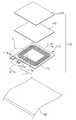
도 1 및 도 2를 참조하면, 본 실시예에 따른 전자 기기는 휴대용 기기(10)나 충전 기기(20)일 수 있으며, 또한 휴대용 기기(10)나 충전 기기(20)에 구비되는 무접점 전력 수신 장치(100)나 무접점 전력 송신 장치(200)일 수 있다.1 and 2, the electronic device according to the present embodiment may be the
휴대용 기기(10)는 배터리(12)와, 배터리(12)에 전력을 공급하여 배터리(12)를 충전하는 무접점 전력 수신 장치(100)를 포함할 수 있다.The
배터리(12)는 충, 방전이 가능한 2차 전지일 수 있으며, 휴대용 기기(10)에서 착탈 가능하게 구성될 수 있다.The
무접점 전력 수신 장치(100)는 휴대용 기기(10)의 케이스(11)의 내부에 수용되어 케이스(11)의 내부면에 직접 부착되거나, 최대한 인접하게 배치될 수 있다.The
또한 본 실시예에 따른 충전 기기(20)는 휴대용기기(10)의 배터리(12)를 충전시키기 위해 구비된다. 이를 위해 충전 기기(20)는 케이스(21) 내부에 무접점 전력 송신 장치(200)를 구비할 수 있다.In addition, the charging
충전 기기(20)는 외부로부터 공급되는 가정용 교류 전원을 직류 전원으로 변환하고, 직류 전원을 다시 특정 주파수의 교류 전압으로 변환하여 무접점 전력 송신 장치(200)에 제공할 수 있다. 이를 위해 충전 장치(20)는 가정용 교류 전원을 특정 주파수의 교류 전압으로 변환하는 전압 변환부(22)를 구비할 수 있다.The charging
상기한 교류 전압이 무접점 전력 송신 장치(200) 내의 박막 코일(미도시)에 인가되면, 박막 코일 주변의 자기장이 변화된다. 이에 무접점 전력 송신 장치(200)와 인접하게 배치되는 전자 기기(10)의 무접점 전력 수신 장치(100)는 자기장의 변화에 따라 전압이 인가되고, 이로 인해 배터리(12)가 충전된다.
When the AC voltage is applied to a thin film coil (not shown) in the
이하에서는 상기한 휴대용 기기(10)에 구비되는 무접점 전력 수신 장치(100)에 대해 보다 상세히 살펴보기로 한다.Hereinafter, the
도 3은 도 2의 무접점 전력 수신 장치를 개략적으로 도시한 분해 사시도이고, 도 4는 도 3의 B-B'에 따른 분해 단면도이며, 도 5는 도 4의 무접점 전력 수신 장치가 결합된 단면도이다.FIG. 3 is an exploded perspective view schematically illustrating the contactless power receiver of FIG. 2, FIG. 4 is an exploded cross-sectional view taken along line BB ′ of FIG. 3, and FIG. 5 is a view illustrating the contactless power receiver of FIG. It is a cross section.
도 3 내지 도 5를 참조하면, 무접점 전력 수신 장치(100)는 자성부(120) 및 박막 코일(110)를 포함하여 구성된다.3 to 5, the
자성부(120)는 편평한 판 형상(또는 시트 형상)으로, 박막 코일(110)의 일면에 배치되어 박막 코일(110)에 고정 부착된다. 자성부(120)는 박막 코일(110)의 코일 패턴(113)에 의해 발생하는 자기장의 자로를 효율적으로 형성하기 위해 구비된다. 이를 위해 자성부(120)는 자로가 용이하게 형성될 수 있는 재질로 형성되며, 구체적으로 페라이트 시트(ferrite sheet)가 이용될 수 있다.The
그러나, 본 실시예에 따른 자성부(120)는 상기한 구성으로 한정되지 않으며, 박막 코일(110)의 일면에 페라이트 가루나 자성체 용액을 도포하여 형성하는 등 다양한 응용이 가능하다.However, the
한편, 도시되어 있지 않지만, 자성부(120)의 외부면에는 전자파나 누설 자속을 자폐하기 위해 필요에 따라 금속 시트를 더 부가하는 것도 가능하다. 금속 시트는 알루미늄(aluminum) 등으로 이루어질 수 있으나 이에 한정되지 않는다.Although not shown, a metal sheet may be further added to the outer surface of the
또한, 본 실시예에 따른 무접점 전력 수신 장치(100)는 박막 코일(110)과 자성부(120)가 서로 견고하게 고정 접착되도록, 박막 코일(110)과 자성부(120) 사이에 접착부(140)가 개재될 수 있다.In addition, in the
접착부(140)는 박막 코일(110)과 자성부(120)의 사이에 배치되며, 자성부(120)와 박막 코일(110)를 상호 접합시킨다. 이러한 접착부(140)는 접착 시트(sheet)나 접착 테이프에 의해 형성될 수 있으며, 기판(112)이나 자성부(120)의 표면에 접착제나 접착성을 갖는 수지를 도포하여 형성할 수도 있다. 이때, 접착부(140)가 페라이트 분말을 함유하도록 구성하여 접착부(140)가 자성부(120)와 함께 자성을 갖도록 구성하는 것도 가능하다.
The
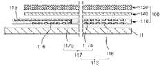
박막 코일(110)는 기판(112)과, 기판(112) 상에 형성되는 코일 패턴(113)을 포함하여 구성될 수 있다.The
본 실시예에 따른 박막 코일(110)의 기판(112)은 박막 기판으로, 예를 들어 유연성 기판(Flexible PCB)일 수 있다. 그러나, 본 발명은 이에 한정되지 않으며, 필름이나 박형의 인쇄 회로 기판 등 두께가 얇고 배선 패턴을 형성할 수 있는 기판이라면 다양하게 이용될 수 있다.The
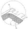
도 6은 도 3의 C 부분을 확대하여 도시한 부분 사시도이고, 도 7은 본 발명의 실시예에 따른 박막 코일의 하부면을 도시한 사시도이다. 또한 도 8은 도 7의 E 부분을 확대하여 도시한 부분 사시도이고, 도 9는 도 6의 D-D'에 따른 단면을 도시한 부분 단면도이다.6 is an enlarged partial perspective view of portion C of FIG. 3, and FIG. 7 is a perspective view illustrating a bottom surface of the thin film coil according to the exemplary embodiment of the present invention. 8 is an enlarged partial perspective view of portion E of FIG. 7, and FIG. 9 is a partial cross-sectional view of a cross section taken along line D-D ′ of FIG. 6.
이를 함께 참조하면, 본 실시예에 따른 코일 패턴(113)은 기판(112)의 양면에 배선 패턴의 형태로 형성되며, 기판(112)이 형성하는 평면 상에서 나선 형상을 그리며 형성될 수 있다.Referring to this together, the
코일 패턴(113)은 나란하게 배치되는 다수의 코일 가닥(117, 118)을 포함할 수 있다. 이때, 각각의 코일 가닥(117, 118)들은 서로 병렬로 연결되어 하나의 코일 패턴(113)을 형성할 수 있다. 본 실시예의 경우, 코일 가닥(117, 118)이 기판(112)의 양면에 각각 형성되어 하나의 코일 패턴(113)을 형성한다.The
코일 가닥들(117, 118)을 병렬로 연결하기 위해, 본 실시예에 따른 박막 코일(110)은 도전성의 연결 비아(114)를 다수 개 구비할 수 있다. 연결 비아(114)는 코일 가닥(117, 118)의 양단에서 코일 가닥(117, 118)들을 상호 간에 전기적으로 연결할 수 있다.In order to connect the
도 6에 도시된 바와 같이 본 실시예에서는 연결 비아(114)가 접촉 패드(119)와 나선형 패턴(117a)의 내측 끝단에 각각 형성되는 경우를 예로 들고 있다. 그러나 본 발명이 이에 한정되는 것은 아니며 코일 패턴(113)의 형상이나 구조에 따라 다양한 위치에 다양한 크기와 다양한 형상으로 형성될 수 있다.As shown in FIG. 6, the connection via 114 is formed at the inner ends of the
또한, 본 실시예에 따른 코일 패턴(113)은 기판(112)의 양면에 형성되는 코일 가닥(117, 118) 중 어느 하나(이하, 제1 코일 가닥)가 나선형의 패턴(117a)과, 나선형 패턴(117a)의 내부에 배치되는 일단에서 나선형 패턴(117a)을 가로지르도록 배치되는 인출 패턴(117d)을 포함할 수 있다.In the
인출 패턴(117d)은 나선형 패턴(117a)의 끝단을 코일 패턴(113)의 외부 즉 후술되는 접촉 패드(119)로 연결하기 위해 구비된다. 따라서 인출 패턴(117d)은 가장 내측에 배치된 나선형 패턴(117a)의 끝단과 접촉 패드(119)를 전기적으로 연결하는 패턴의 형태로 형성된다.The
이에 따라, 도 9에 된 바와 같이 제1 코일 가닥(117)의 나선형 패턴(117a)은 인출 패턴(117d)이 배치되는 부분에서 인출 패턴(117d)을 중심으로 선회하도록 형성된다. 즉, 제1 코일 가닥(117)의 나선형 패턴(117a)은 인출 패턴(117d)이 배치된 부분에서 기판(112)의 타면을 경유하는 적어도 하나의 선회 경로가 형성되며, 이에 나선형 패턴(117a)은 인출 패턴(117d)과의 간섭 없이 코일 형상을 유지할 수 있다.Accordingly, as shown in FIG. 9, the
선회 경로는 기판(112)의 타면에 배치되는 코일 가닥(이하 제2 코일 가닥)과 접촉하지 않도록 형성될 수 있다(도시되지 않음). 이 경우, 선회 경로는 제2 코일 가닥(118)의 사이 공간에 배치될 수 있다.The pivot path may be formed so as not to contact the coil strand (hereinafter, the second coil strand) disposed on the other surface of the substrate 112 (not shown). In this case, the turning path may be disposed in the space between the
그러나 이러한 경우 선회 경로에 의해 박막 코일의 전체 면적이 증가하게 되는 단점이 있다.In this case, however, the entire area of the thin film coil is increased by the turning path.
따라서 본 실시예에 따른 박막 코일(100)은 제2 코일 가닥(118)을 이용하여 선회 경로를 형성한다. 즉, 본 실시예에 따른 선회 경로는 제2 코일 가닥(118)을 부분적으로 공유하도록 구성된다.Therefore, the
도 6 및 도 9에 도시된 바와 같이, 본 실시예에 따른 나선형 패턴(117a)은 인출 패턴(117d)에 의해 단절되는 부분에 도전성의 선회용 비아(115)들이 배치된다. 선회용 비아(115)에 의해 제1 코일 가닥(117)은 제2 코일 가닥(118)과 전기적으로 연결된다.6 and 9, in the
이에, 본 실시예에 따른 하나의 선회 경로는 두 개의 선회용 비아(115)와, 선회용 비아(115)들 사이에 배치되는 제2 코일 가닥(118)의 일부분(도 9의 S, 이하 공유 구간)을 포함하여 구성될 수 있다. 이러한 선회 경로는 나선형 패턴(117a)의 권선수에 대응하는 수만큼 형성될 수 있다.Thus, one pivot path according to the present embodiment is a portion of the
또한 본 실시예에 따른 코일 패턴(113)은 제1 코일 가닥(117)과 제2 코일 가닥(118)이 기판(112)을 매개로 서로 투영되는 위치(즉, 수직 방향으로 대응되는 위치)에 배치된다. 따라서, 선회용 비아(115)가 기판(112)에 수직하게 형성되는 경우, 제1 코일 가닥(117)과 제2 코일 가닥(118)은 선회용 비아(115)에 의해 서로 대응하는 패턴과 용이하게 전기적으로 연결될 수 있다.In addition, the
이러한 구성으로 인해, 본 실시예에 따른 코일 패턴(113)은 인출 패턴(117d)이 형성된 위치까지는 제1, 제2 코일 가닥(117, 118)이 기판(112)의 양면에 독립적으로 배치되나, 인출 패턴(117d)이 형성된 부분에서는 기판(112) 타면의 제2 코일 가닥(118)을 함께 공유하게 된다.Due to this configuration, in the
이에 코일 패턴(113)은 각 코일 가닥들(117, 118)이 패턴의 양단에서만 전기적으로 연결되는 구조가 아닌, 패턴의 중간에서 코일 패턴(113)의 권선 횟수만큼 코일 가닥(117, 118)들이 서로 전기적으로 연결되는 구조를 갖는다.Thus, the
한편, 본 실시예의 경우 기판(112)의 상면에 형성되는 제1 코일 가닥(117)에 인출 패턴(117d)이 형성되는 경우를 예로 들고 있다. 그러나 본 발명이 이에 한정되는 것은 아니며, 기판(112)의 상면이 아닌, 하면 즉 제2 코일 가닥(118)에 인출 패턴을 형성하는 것도 가능하다.Meanwhile, in the present embodiment, the case where the
또한, 본 실시예에서는 기판(112)의 양면에 형성되는 각각의 코일 가닥들(117, 118)이 기판(112)을 매개로 서로 투영되는 위치에 형성되는 경우를 예로 들었으나, 본 발명은 이에 한정되지 않는다. 즉, 기판(112)의 각 면에 형성되는 각각의 코일 가닥(117, 118)이 서로 투영되는 위치가 아닌, 서로 어긋나는 위치에 형성되도록 구성하는 등 필요에 따라 다양한 응용이 가능하다. 이 경우, 선회용 비아는 코일 가닥들을 연결하기 위해 기판에 수직이 아닌 비스듬한 방향 또는 계단 형태로 형성될 수 있다.In addition, in the present exemplary embodiment, the
또한 본 실시예에서는 코일 패턴(113)이 전체적으로 사각형의 나선 형상으로 형성되는 경우를 예로 들고 있으나, 본 발명은 이에 한정되지 않으며, 원형이나 다각형의 나선 형상으로 형성하는 등 다양한 응용이 가능하다.In addition, in the present embodiment, the
더하여, 코일 패턴(113)의 상부에는 필요에 따라 코일 패턴(113)을 외부로부터 보호하기 위한 절연 보호층(예컨대, 수지 절연층, 도시되지 않음)이 부가될 수 있다.In addition, an insulating protective layer (eg, a resin insulating layer, not shown) may be added to the upper portion of the
한편, 기판(112)의 일측, 즉 코일 패턴(113)의 외부에는 코일 패턴(113)을 외부와 전기적으로 연결하기 위한 접촉 패드(119)가 형성될 수 있다.Meanwhile, a
접촉 패드(119)는 코일 패턴(113)의 양단이 각각 전기적으로 연결되며, 이를 위해 적어도 두 개가 구비될 수 있다.Both ends of the
또한 본 실시예에 따른 접촉 패드(119)는 코일 패턴(113)의 외측에 모두 배치된다. 이처럼 접촉 패드(119)가 모두 코일 패턴(113)의 외측에 배치되더라도, 본 실시예에 따른 박막 코일은 전술한 선회 경로와 인출 패턴(117d)을 통해 코일 패턴(113)의 양단이 모두 접촉 패드(119)에 용이하게 연결될 수 있다.In addition, the
또한 도 6 등에 도시된 바와 같이, 본 실시예에 따른 접촉 패드(119)는 사각 형상의 기판(112)에서 기판(112)의 일측으로 돌출되는 형태로 배치될 수 있다. 이 로 인해, 본 실시예에 따른 접촉 패드(119)는 박막 코일(110)과 자성부(120)가 결합되더라도 자성부(120)의 외부로 노출된다.In addition, as shown in FIG. 6, the
따라서 본 실시예에 따른 박막 코일(110)은 자성부(120)와 결합된 후에도 코일 패턴(113)과 다른 구성 요소(예컨대 배터리나 전압 변환부 등)들을 용이하게 전기적으로 연결할 수 있다.
Therefore, the
한편, 본 실시예에서는 기판(112)의 각 면에 형성되는 코일 가닥들(117, 118)이 각각 하나의 가닥으로 형성되는 경우를 예로 들었으나 본 발명이 이에 한정되는 것은 아니며, 후술되는 다른 실시예와 같이 다수의 가닥으로 형성될 수도 있다.Meanwhile, in the present exemplary embodiment, the
또한, 본 실시예에 따른 박막 코일(110)은 기판(112)의 한 면에 형성될 수 있는 코일 가닥(117, 118)의 개수가 기판(112)의 크기, 즉 전자 기기의 크기에 따라 설정될 수 있다.In addition, in the
즉, 기판(112)의 크기가 크게 형성되는 경우, 기판(112)의 한 면에는 도 10에 도시된 바와 같이 하나가 아닌 다수의 코일 가닥이 형성될 수 있으며, 기판(112)의 크기가 작게 형성되는 경우, 기판(112)의 한 면에는 본 실시예와 같이 하나의 코일 가닥(117, 118)만이 형성될 수 있다.That is, when the size of the
또한 도시되어 있지 않지만, 본 실시예에 따른 무접점 전력 수신 장치(100)는 박막 코일(110)의 코일 패턴(113)에서 발생되는 전력을 전자 기기(10)의 배터리(도 2의 12)로 제공하기 위해, 박막 코일(110)의 접촉 패드(119)와 배터리를 전기적으로 연결하는 연결 부재를 더 포함할 수 있다.Also, although not shown, the
연결 부재는 도전성 와이어가 이용될 수 있으며, 내부에 배선 패턴이 형성된 박막의 회로 기판(예컨대 유연성 기판)이 이용될 수도 있다.
A conductive wire may be used as the connecting member, and a thin film circuit board (for example, a flexible board) having a wiring pattern formed therein may be used.
이러한 본 실시예에 따른 무접점 전력 수신 장치(100)는 종래와 같이 와이어(wire) 형태의 코일을 이용하지 않고, 얇은 박막 기판(112) 상에 코일 패턴(113)을 형성하여 이용하므로, 박막 코일(110)의 두께를 매우 얇게 형성하는 것이 가능하다.Since the
또한, 본 실시예에 따른 박막 코일(110)는 병렬로 연결되는 다수의 코일 가닥(117, 118)들에 의해 하나의 코일 패턴(113)이 형성된다. 이에 따라, 본 실시예에 따른 코일 패턴(113)은 기판(112) 상에 패턴 형태로 형성되지만, 여러 가닥의 전선을 꼬아 형성한 연선(撚線) 형태의 코일(예컨대 리쯔 와이어, Litz wire)을 이용하는 효과를 도출할 수 있다. 이와 같이 연선 형태의 코일을 이용하는 경우, 낮은 주파수에서 맴돌이 전류(eddy current)와 표피 효과(skin effect) 등에 의해 발생되는 손실(예컨대, 교류 저항값 등)을 최소화할 수 있다.In addition, in the
이처럼 본 실시예에 따른 무접점 전력 수신 장치(100)는 코일 패턴(113)을 연선 형태로 형성하더라도 박막 코일(110)의 두께를 최소화(예컨대, 0.1mm 이하)할 수 있어, 무접점 전력 수신 장치(100)의 전체적인 두께를 줄일 수 있다.As described above, the
더하여, 본 실시예에 따른 무접점 전력 수신 장치(100)는 박막 코일의 접촉 패드(119)가 모두 기판(112)의 측면에 배치된다. 또한 접촉 패드(119)를 기판(112)의 측면으로 배치하기 위해 기판(112)에 별도의 구성이 부가되지 않는다는 이점이 있다. 이에 대해 설명하면 다음과 같다.In addition, in the
코일 패턴(113)의 양단에 연결되는 접촉 패드(119)들 중, 코일 패턴(113)의 내부(즉 중심)을 향해 권선되는 코일 패턴(113)에 연결되는 접촉 패드(119)는 코일 패턴(113)의 외측이 아닌, 패턴 내부에 배치되기 쉽다. 이러한 경우, 코일 패턴(113)의 내부에 배치되는 접촉 패드는 별도의 도전성 와이어나 연결용 기판(예컨대 FPCB) 등을 통해 외부와 전기적으로 연결되어야 한다.Among the
또한, 본 발명과 같이 접촉 패드를 코일 패턴(113)의 외부에 배치하기 위해서는 코일 패턴(113) 위에 절연 물질로 브릿지를 형성하여 패턴을 만들거나, 기판(112)으로 여러 층이 적층된 다층 기판을 이용해야 한다.In addition, in order to arrange the contact pad outside the
이러한 경우 기판 상에 브릿지를 형성하거나, 다층 기판을 제조하기 위해 제조 시간이나 제조 비용이 부가적으로 소요되며, 기판(112)의 전체적인 두께도 두꺼워지게 된다.In this case, it takes additional manufacturing time or manufacturing cost to form a bridge on the substrate or to manufacture a multilayer substrate, and the overall thickness of the
그러나 본 실시예에 따른 박막 코일(100)은 다층 기판이나 브릿지를 이용하지 않더라도 접촉 패드(119)를 모두 코일 패턴(113)의 외부에 배치할 수 있다. 따라서 상기한 경우에 비해 제조 시간이나 제조 비용을 줄일 수 있으며 박막 코일(100)이나 무접점 전력 수신 장치(100)의 두께가 두꺼워지는 것을 방지할 수 있다.However, in the
한편 이상에서 설명한 박막 코일(100)의 구성은 충전 장치(20)에 구비되는 무접점 전력 송신 장치(200)에도 동일하게 적용될 수 있다. 따라서, 무접점 전력 송신 장치(200)에 대한 구체적인 설명은 생략하기로 한다.
Meanwhile, the configuration of the
이하에서 설명하는 실시예에 따른 박막 코일은 전술된 실시예의 의 박막 코일(도 6의 110)과 유사한 구조로 구성되며, 코일 패턴의 형태에 있어서만 차이를 갖는다. 따라서 동일한 구성요소들에 대해서는 동일한 도면 부호를 사용하고 상세한 설명은 생략하며, 코일 패턴의 형태를 중심으로 하여 보다 상세하게 설명하기로 한다.
The thin film coil according to the embodiment described below has a structure similar to that of the thin film coil (110 of FIG. 6) of the above-described embodiment, and has a difference only in the form of the coil pattern. Therefore, the same reference numerals are used for the same components, and detailed descriptions thereof will be omitted, and will be described in more detail with reference to the shape of the coil pattern.
도 10은 본 발명의 다른 실시예에 따른 박막 코일을 개략적으로 도시한 사시도이다.10 is a perspective view schematically showing a thin film coil according to another embodiment of the present invention.
도 10을 참조하면, 본 실시예에 따른 박막 코일(110)는 전술한 실시예와 같이 박막의 기판(112)과, 기판(112) 상에 형성되는 코일 패턴(113)을 포함하여 구성될 수 있다.Referring to FIG. 10, the
본 실시예에 따른 코일 패턴(113)은 나란하게 배치되는 다수의 코일 가닥(117a~117c)을 포함한다. 이때, 다수의 코일 가닥들(117a~117c)은 모두 동일한 접촉 패드(119)에 전기적으로 연결된다. 이에 따라, 각각의 코일 가닥들(117a~117c)은 서로 병렬로 연결되어 하나의 코일 패턴(113)을 형성하게 된다.The
본 실시예의 경우, 기판(112)의 일면에 코일 패턴(113)이 3개의 코일 가닥(117a~117c)으로 형성되는 경우를 예로 들고 있다. 이 경우, 코일 패턴(113)의 각 코일 가닥들(117a~117c)은 일정한 간격으로 이격되어 나란하게 배치된다.In the present embodiment, a case in which the
전술한 실시예와 마찬가지로, 본 실시예에 따른 코일 패턴(113)도 인출 패턴(117d)과 다수의 선회용 비아(115)를 포함한다. 따라서 다층기판이나 브릿지를 사용할 필요가 없으므로 기판(112) 두께의 증가 없이 접촉 패드(119)를 코일 패턴(113)의 외부에 배치할 수 있어 박막 코일이나 무접점 전력 수신 장치의 전체적인 두께를 줄일 수 있으며, 제조 시간이나 제조 비용을 줄일 수 있다.Similar to the above-described embodiment, the
한편 도 10에서는 인출 패턴(117d)이 하나의 코일 가닥으로 형성되는 경우를 예로 들고 있다. 그러나 본 발명이 이에 한정되는 것은 아니며 인출 패턴(117d)도 코일 패턴(113)의 다른 부분과 마찬가지로 다수의 코일 가닥으로 형성하는 것도 가능하다.10 illustrates a case where the
또한 기판(112)의 하면에 형성되는 코일 가닥(도시되지 않음)의 경우, 기판(112)의 상면에 형성되는 코일 가닥(117a~117c)과 마찬가지로 다수 개로 형성될 수 있다. 그러나 본 발명이 이에 한정되는 것은 아니다. 즉, 넓은 폭을 갖는 하나의 코일 가닥만을 기판(112) 하부에 형성하는 등 기판(112) 상면에 형성되는 코일 가닥(117a~117c)이 선회용 비아(115)를 통해 기판(112) 하면의 코일 가닥과 전기적으로 연결될 수만 있다면 필요에 따라 다양한 형태로 형성될 수 있다.
In addition, in the case of coil strands (not shown) formed on the lower surface of the
이상에서 설명한 본 발명에 따른 박막 코일 및 이를 구비하는 전자 기기는 전술한 실시예들에 한정되지 않으며, 다양한 응용이 가능하다. 예를 들어, 전술한 실시예들에서는 박막 코일의 접촉 패드가 기판의 동일한 방향으로 배치되는 경우를 예로 들었으나, 필요에 따라 기판의 양측으로 배치하는 등 다양한 응용이 가능하다.The thin film coil and the electronic device having the same according to the present invention described above are not limited to the above-described embodiments, and various applications are possible. For example, in the above-described embodiments, the contact pads of the thin film coil are disposed in the same direction of the substrate. However, various applications may be possible, such as disposed on both sides of the substrate as necessary.
또한, 전술한 실시예들에서는 전자 기기의 무접점 전력 전송 장치에 구비되는 박막 코일을 예로 들어 설명하였다.In the above-described embodiments, the thin film coil provided in the contactless power transmission device of the electronic device has been described as an example.
그러나 본 발명이 이에 한정되는 것은 아니며, 변압기나 모터 등과 같이 코일이 이용되는 전자 부품이나 전자 기기에 폭넓게 적용될 수 있다.However, the present invention is not limited thereto, and the present invention may be widely applied to an electronic component or an electronic device using a coil such as a transformer or a motor.
10.....전자 기기
11, 12.....케이스
12.....배터리20.....충전 기기
100.....무접점 전력 수신 장치
110.....박막 코일112.....기판
113.....코일 패턴
114.....연결 비아115.....선회용 비아
117.....제1 코일 가닥
117a.....나선형 패턴 117d.....인출 패턴
118.....제2 코일 가닥
120.....자성부140.....접착부
200.....무접점 전력 송신 장치10 ..... Electronic devices
11, 12 ... case
12 .....
100 ..... Solid State Power Receiver
110 .....
113 ..... coil pattern
114 ..... Connecting vias 115 ..... Slewing vias
117 ..... 1st coil strand
117a .....
118 ..... the second coil strand
120 ..... magnetic 140 ..... adhesive
200 ..... Solid state power transmitter
Claims (16)
Translated fromKorean상기 기판의 양면에 각각 형성되는 제1 코일 가닥, 제2 코일 가닥을 포함하는 코일 패턴;
을 포함하며,
상기 기판의 일면에 형성되는 상기 제1 코일 가닥은 상기 기판의 타면을 경유하며 선회하는 적어도 하나의 선회 경로를 포함하며,
상기 선회 경로는 상기 기판의 타면에 형성되는 상기 제2 코일 가닥을 부분적으로 공유하는 박막 코일.
Board; And
A coil pattern including first coil strands and second coil strands respectively formed on both surfaces of the substrate;
/ RTI >
The first coil strand formed on one surface of the substrate includes at least one pivot path for pivoting through the other surface of the substrate,
And the pivot path partially shares the second coil strand formed on the other surface of the substrate.
선회용 비아를 통해 상기 제1 코일 가닥이 상기 제2 코일 가닥과 연결되어 형성되는 박막 코일.
The method of claim 1, wherein the turning path,
The thin film coil formed by connecting the first coil strand with the second coil strand through a pivoting via.
상기 제1 코일 가닥과 상기 제2 코일 가닥을 전기적으로 연결하는 두 개의 선회용 비아; 및
상기 제2 코일 가닥 중 상기 두 개의 선회용 비아들 사이에 배치되는 공유 구간;
을 포함하여 구성되는 박막 코일.
The method of claim 1, wherein at least one of the pivot paths is:
Two pivoting vias electrically connecting the first coil strand and the second coil strand; And
A sharing section disposed between the two pivoting vias of the second coil strand;
Thin film coil is configured to include.
상기 코일 패턴의 외측에 배치되며, 상기 코일 패턴의 양단이 각각 전기적으로 연결되는 두 개의 접촉 패드를 더 포함하는 박막 코일.
The method of claim 1,
The thin film coil disposed on the outer side of the coil pattern, further comprising two contact pads, each end of which is electrically connected.
상기 기판의 일면 중 상기 선회 경로에 대응하는 부분을 통해 일단이 상기 접촉 패드와 전기적으로 연결되는 박막 코일.
The method of claim 5, wherein the first coil strand,
A thin film coil having one end electrically connected to the contact pad through a portion of one surface of the substrate corresponding to the pivot path.
상호 간에 병렬로 연결되는 박막 코일.
The method of claim 1, wherein the first coil strand and the second coil strand,
Thin film coils connected in parallel to each other.
양 끝단에 각각 도전성의 연결 비아가 배치되며, 상기 연결 비아에 의해 상기 제1 코일 가닥과 전기적으로 연결되는 박막 코일.
The method of claim 1, wherein the second coil strand,
A conductive connecting via is disposed at both ends, respectively, and the thin film coil is electrically connected to the first coil strand by the connecting via.
상기 기판의 양면에서 수직 방향으로 대응하는 위치에 배치되는 박막 코일.
The method of claim 1, wherein the first coil strand and the second coil strand,
And a thin film coil disposed at corresponding positions in the vertical direction on both sides of the substrate.
상기 기판의 양면에 각각 형성되는 제1 코일 가닥, 제2 코일 가닥을 포함하는 코일 패턴; 및
상기 코일 패턴의 외측에 배치되며 상기 코일 패턴의 양단이 각각 전기적으로 연결되는 두 개의 접촉 패드;
를 포함하고,
상기 기판의 일면에 형성되는 상기 제1 코일 가닥은,
나선형 패턴; 및
상기 나선형 패턴의 내부에 배치되는 일단에서 상기 나선형 패턴을 가로지르도록 배치되어 상기 접촉 패드와 전기적으로 연결되는 인출 패턴;
을 포함하는 박막 코일.
Board;
A coil pattern including first coil strands and second coil strands respectively formed on both surfaces of the substrate; And
Two contact pads disposed outside the coil pattern and electrically connected to both ends of the coil pattern;
Lt; / RTI >
The first coil strand is formed on one surface of the substrate,
Spiral pattern; And
A drawing pattern disposed across the spiral pattern at one end of the spiral pattern and electrically connected to the contact pads;
Thin film coil comprising a.
상기 인출 패턴이 배치되는 부분이 상기 기판의 타면을 경유하며 상기 인출 패턴을 중심으로 선회하는 박막 코일.
The method of claim 10, wherein the spiral pattern of the first coil strand,
And a portion in which the drawing pattern is disposed pivots about the drawing pattern via the other surface of the substrate.
상기 선회하는 부분이 상기 기판의 타면에 형성되는 제2 코일 가닥을 부분적으로 공유하는 박막 코일.
The method of claim 11, wherein the first coil,
And the pivot portion partially shares a second coil strand formed on the other surface of the substrate.
내부에 상기 무접점 전력 전송 장치를 수용하는 케이스;
를 포함하는 전자 기기.
The first coil strand and the second coil strand are disposed on both sides of the substrate so that the first coil strand and the second coil strand are connected in parallel, respectively, and the first coil strand formed on one surface of the substrate has at least one pivot path pivoting through the other surface of the substrate. A contactless power transmission device including a thin film coil, wherein the pivot path partially shares the second coil strand formed on the other surface of the substrate; And
A case accommodating the contactless power transmission device therein;
.
상기 케이스의 내부면에 직접 부착되거나 최대한 인접하게 배치되는 전자 기기.
The apparatus of claim 13, wherein the contactless power transmission device,
Electronic device directly attached to the inner surface of the case or disposed as close as possible.
상기 무접점 전력 전송 장치에서 발생되는 전력을 저장하는 배터리를 더 포함하는 전자 기기.
The method of claim 13,
And a battery storing power generated by the contactless power transmitter.
외부로부터 공급되는 교류 전원을 특정 주파수의 교류 전압으로 변환하여 상기 무접점 전력 전송 장치로 제공하는 전압 변환부를 더 포함하는 전자 기기.The method of claim 13,
And a voltage converter converting an AC power supplied from the outside into an AC voltage having a specific frequency and providing the same to the contactless power transmitter.
Priority Applications (9)
| Application Number | Priority Date | Filing Date | Title |
|---|---|---|---|
| KR1020120032341AKR101339486B1 (en) | 2012-03-29 | 2012-03-29 | Thin film coil and electronic device having the same |
| JP2012123508AJP2013207297A (en) | 2012-03-29 | 2012-05-30 | Thin film coil and electronic device having the same |
| EP12275087.0AEP2645385A2 (en) | 2012-03-29 | 2012-06-06 | Thin film coil and electronic device having the same |
| CN201210189520.2ACN103366931B (en) | 2012-03-29 | 2012-06-08 | Film coil and the electronic installation with this film coil |
| US13/533,560US9165708B2 (en) | 2012-03-29 | 2012-06-26 | Thin film coil and electronic device having the same |
| JP2014046233AJP2014112728A (en) | 2012-03-29 | 2014-03-10 | Thin film coil and electronic device having the same |
| US14/859,885US10483767B2 (en) | 2012-03-29 | 2015-09-21 | Thin film coil and electronic device having the same |
| US15/654,092US10122183B2 (en) | 2012-03-29 | 2017-07-19 | Thin film coil and electronic device having the same |
| US15/653,725US10103554B2 (en) | 2012-03-29 | 2017-07-19 | Thin film coil and electronic device having the same |
Applications Claiming Priority (1)
| Application Number | Priority Date | Filing Date | Title |
|---|---|---|---|
| KR1020120032341AKR101339486B1 (en) | 2012-03-29 | 2012-03-29 | Thin film coil and electronic device having the same |
Related Child Applications (1)
| Application Number | Title | Priority Date | Filing Date |
|---|---|---|---|
| KR1020130073008ADivisionKR20130111489A (en) | 2013-06-25 | 2013-06-25 | Thin film coil and electronic device having the same |
Publications (2)
| Publication Number | Publication Date |
|---|---|
| KR20130110397A KR20130110397A (en) | 2013-10-10 |
| KR101339486B1true KR101339486B1 (en) | 2013-12-10 |
Family
ID=46508300
Family Applications (1)
| Application Number | Title | Priority Date | Filing Date |
|---|---|---|---|
| KR1020120032341AActiveKR101339486B1 (en) | 2012-03-29 | 2012-03-29 | Thin film coil and electronic device having the same |
Country Status (5)
| Country | Link |
|---|---|
| US (4) | US9165708B2 (en) |
| EP (1) | EP2645385A2 (en) |
| JP (2) | JP2013207297A (en) |
| KR (1) | KR101339486B1 (en) |
| CN (1) | CN103366931B (en) |
Cited By (1)
| Publication number | Priority date | Publication date | Assignee | Title |
|---|---|---|---|---|
| KR102203609B1 (en)* | 2019-10-18 | 2021-01-15 | 한국표준과학연구원 | Electromagnetic acoustic transducer and pipe inspection apparatus comprising the same |
Families Citing this family (75)
| Publication number | Priority date | Publication date | Assignee | Title |
|---|---|---|---|---|
| US11476566B2 (en)* | 2009-03-09 | 2022-10-18 | Nucurrent, Inc. | Multi-layer-multi-turn structure for high efficiency wireless communication |
| CN107275763B (en)* | 2012-03-23 | 2020-07-28 | Lg 伊诺特有限公司 | Antenna assembly |
| TWI604480B (en) | 2012-03-23 | 2017-11-01 | Lg伊諾特股份有限公司 | Wireless power receiver and portable terminal comprising the same |
| US10658869B2 (en)* | 2012-08-03 | 2020-05-19 | Mediatek Inc. | Multi-mode, multi-standard wireless power transmitter coil assembly |
| WO2014092492A1 (en)* | 2012-12-12 | 2014-06-19 | 엘에스전선 주식회사 | Antenna for wireless power, and dual mode antenna comprising same |
| KR20150023837A (en)* | 2013-03-06 | 2015-03-05 | 가부시키가이샤 헤즈 | Contactless power supply device |
| JP6306288B2 (en)* | 2013-05-13 | 2018-04-04 | 日東電工株式会社 | Coil printed wiring board, power receiving module, battery unit and power receiving communication module |
| KR102017669B1 (en)* | 2013-08-29 | 2019-10-21 | 주식회사 위츠 | Coil type unit for wireless power transmission, wireless power transmission device, electronic device and manufacturing method of coil type unit for wireless power transmission |
| KR101407205B1 (en)* | 2013-10-21 | 2014-06-12 | (주)디아이디 | Coil resonator for wireless power transmission of magnetic resonance and method of fabricating the same |
| US10020683B2 (en) | 2013-10-31 | 2018-07-10 | Qualcomm Incorporated | Systems, apparatus, and method for a dual mode wireless power receiver |
| ES2883127T3 (en)* | 2013-11-25 | 2021-12-07 | A K Stamping Co Inc | Wireless charging coil |
| US9490656B2 (en) | 2013-11-25 | 2016-11-08 | A.K. Stamping Company, Inc. | Method of making a wireless charging coil |
| US9859052B2 (en) | 2013-11-25 | 2018-01-02 | A.K. Stamping Co., Inc. | Wireless charging coil |
| CN105448489A (en)* | 2014-08-11 | 2016-03-30 | 介面光电股份有限公司 | Thin film coil, thin film coil assembly and charging device |
| TWI681590B (en) | 2014-08-13 | 2020-01-01 | 瑞士商菲利浦莫里斯製品股份有限公司 | Container of consumer goods, system for operating an electronic device provided on a container of consumer goods and method of forming a container of consumer goods |
| KR101659162B1 (en)* | 2014-09-11 | 2016-09-22 | 삼성전기주식회사 | Non-contact type power charging apparatus |
| CN105655114A (en)* | 2014-11-12 | 2016-06-08 | 介面光电股份有限公司 | Thin film coil element, manufacturing method thereof, and charging device element having the same |
| KR102118352B1 (en)* | 2015-01-07 | 2020-06-04 | 삼성전자주식회사 | Wireless power receiver |
| US10109415B2 (en) | 2015-01-07 | 2018-10-23 | Samsung Electronics Co., Ltd. | Wireless power receiver and external inductor connected thereto |
| KR101832554B1 (en)* | 2015-01-28 | 2018-02-26 | 삼성전기주식회사 | Chip electronic component and manufacturing method thereof |
| US9960629B2 (en)* | 2015-08-07 | 2018-05-01 | Nucurrent, Inc. | Method of operating a single structure multi mode antenna for wireless power transmission using magnetic field coupling |
| US9941729B2 (en)* | 2015-08-07 | 2018-04-10 | Nucurrent, Inc. | Single layer multi mode antenna for wireless power transmission using magnetic field coupling |
| US10658847B2 (en)* | 2015-08-07 | 2020-05-19 | Nucurrent, Inc. | Method of providing a single structure multi mode antenna for wireless power transmission using magnetic field coupling |
| US10636563B2 (en)* | 2015-08-07 | 2020-04-28 | Nucurrent, Inc. | Method of fabricating a single structure multi mode antenna for wireless power transmission using magnetic field coupling |
| US9960628B2 (en) | 2015-08-07 | 2018-05-01 | Nucurrent, Inc. | Single structure multi mode antenna having a single layer structure with coils on opposing sides for wireless power transmission using magnetic field coupling |
| US11205848B2 (en) | 2015-08-07 | 2021-12-21 | Nucurrent, Inc. | Method of providing a single structure multi mode antenna having a unitary body construction for wireless power transmission using magnetic field coupling |
| US9941743B2 (en)* | 2015-08-07 | 2018-04-10 | Nucurrent, Inc. | Single structure multi mode antenna having a unitary body construction for wireless power transmission using magnetic field coupling |
| US9948129B2 (en)* | 2015-08-07 | 2018-04-17 | Nucurrent, Inc. | Single structure multi mode antenna for wireless power transmission using magnetic field coupling having an internal switch circuit |
| US9941590B2 (en)* | 2015-08-07 | 2018-04-10 | Nucurrent, Inc. | Single structure multi mode antenna for wireless power transmission using magnetic field coupling having magnetic shielding |
| US10063100B2 (en)* | 2015-08-07 | 2018-08-28 | Nucurrent, Inc. | Electrical system incorporating a single structure multimode antenna for wireless power transmission using magnetic field coupling |
| US10985465B2 (en) | 2015-08-19 | 2021-04-20 | Nucurrent, Inc. | Multi-mode wireless antenna configurations |
| US10211663B2 (en) | 2015-08-21 | 2019-02-19 | Apple Inc. | 3D shaped inductive charging coil and method of making the same |
| US10923957B2 (en)* | 2015-11-18 | 2021-02-16 | The University Of Hong Kong | Wireless power transfer system |
| US10553345B2 (en) | 2016-03-25 | 2020-02-04 | Wits Co., Ltd. | Coil device and apparatus including the same |
| KR102552028B1 (en) | 2016-03-25 | 2023-07-06 | 주식회사 위츠 | A coil device and an apparatus comprising the same |
| TWI665687B (en)* | 2016-04-28 | 2019-07-11 | 乾坤科技股份有限公司 | Method for producing a wireless charging coil |
| CN107492436B (en) | 2016-06-11 | 2019-11-22 | 宁波微鹅电子科技有限公司 | A kind of induction coil structure and radio energy transmission system |
| KR101912283B1 (en)* | 2016-06-14 | 2018-10-29 | 삼성전기 주식회사 | Coil device and manufacturing method of the same |
| KR20180007745A (en)* | 2016-07-14 | 2018-01-24 | (주)에너브레인 | Method for manufacturing thin film type coil unit for camera actuator |
| US20180062434A1 (en) | 2016-08-26 | 2018-03-01 | Nucurrent, Inc. | Wireless Connector Receiver Module Circuit |
| US10622820B2 (en)* | 2016-09-23 | 2020-04-14 | Apple Inc. | Bobbin structure and transmitter coil for wireless charging mats |
| US10432031B2 (en) | 2016-12-09 | 2019-10-01 | Nucurrent, Inc. | Antenna having a substrate configured to facilitate through-metal energy transfer via near field magnetic coupling |
| FR3061999B1 (en)* | 2017-01-19 | 2019-08-23 | Institut Vedecom | WIRELESS CHARGING PANEL, EQUIPPED ENERGY STORAGE UNIT AND CHARGEABLE POWER SUPPLY SYSTEM |
| US11502547B2 (en) | 2017-02-13 | 2022-11-15 | Nucurrent, Inc. | Wireless electrical energy transmission system with transmitting antenna having magnetic field shielding panes |
| US11605487B2 (en)* | 2017-04-14 | 2023-03-14 | The Diller Corporation | Laminate with induction coils and charging station device comprising same |
| US11283295B2 (en) | 2017-05-26 | 2022-03-22 | Nucurrent, Inc. | Device orientation independent wireless transmission system |
| US12159745B2 (en)* | 2017-05-30 | 2024-12-03 | InductEV, Inc. | Wireless power transfer thin profile coil assembly |
| US10390468B2 (en) | 2017-08-25 | 2019-08-20 | Qualcomm Incorporated | Wireless power-transmission shield |
| US11268988B2 (en)* | 2017-11-24 | 2022-03-08 | Shindengen Electric Manufacturing Co., Ltd. | Detection substrate, assembly, and method for manufacturing detection substrate |
| KR101901715B1 (en)* | 2018-02-14 | 2018-09-27 | 삼성전기 주식회사 | Antenna module and electronic device having the same |
| JP2018121066A (en)* | 2018-03-08 | 2018-08-02 | 日東電工株式会社 | Coil printed wiring board, power receiving module, battery unit, and power receiving communication module |
| CN108565102B (en) | 2018-03-28 | 2020-08-14 | 华为技术有限公司 | Coil module, wireless charging transmitter, receiver, system and terminal |
| CN108735439B (en)* | 2018-05-25 | 2023-11-17 | 昆山联滔电子有限公司 | Film coil and electronic device |
| CN109036803A (en)* | 2018-06-15 | 2018-12-18 | 上海安费诺永亿通讯电子有限公司 | Coil, wireless power transmitters and receivers, near-field communication device and electronic equipment |
| CN109411210B (en)* | 2018-07-24 | 2024-07-09 | 昆山联滔电子有限公司 | Wire winding device |
| CN109961942B (en) | 2018-08-04 | 2020-06-16 | 华为技术有限公司 | Coil module, wireless charging transmitting device, wireless charging receiving device, wireless charging system and wireless charging terminal |
| JP2020053522A (en)* | 2018-09-26 | 2020-04-02 | 矢崎総業株式会社 | Power transmission unit |
| KR102596514B1 (en) | 2018-10-15 | 2023-11-01 | 삼성전자주식회사 | Electronic device including wireless charging coil and structure thereof |
| US12249847B2 (en) | 2018-12-31 | 2025-03-11 | 3M Innovative Properties Company | Wireless power transfer |
| US11271430B2 (en) | 2019-07-19 | 2022-03-08 | Nucurrent, Inc. | Wireless power transfer system with extended wireless charging range |
| US11227712B2 (en) | 2019-07-19 | 2022-01-18 | Nucurrent, Inc. | Preemptive thermal mitigation for wireless power systems |
| EP3786985B1 (en) | 2019-08-28 | 2023-06-07 | Delta Electronics (Thailand) Public Co., Ltd. | Resonating inductor for wireless power transfer |
| KR102269280B1 (en) | 2019-09-06 | 2021-06-24 | 엘지전자 주식회사 | Coil device and apparatus including the same |
| US11056922B1 (en) | 2020-01-03 | 2021-07-06 | Nucurrent, Inc. | Wireless power transfer system for simultaneous transfer to multiple devices |
| WO2021167398A1 (en)* | 2020-02-20 | 2021-08-26 | 주식회사 아모센스 | Magnetic shielding sheet and manufacturing method therefor |
| US11528806B2 (en)* | 2020-02-22 | 2022-12-13 | Kla Corporation | Electromagnet coils made from flexible circuits |
| US11502545B2 (en) | 2020-05-29 | 2022-11-15 | Puthalath Koroth Raghuprasad | Watch charging assembly |
| US11283303B2 (en) | 2020-07-24 | 2022-03-22 | Nucurrent, Inc. | Area-apportioned wireless power antenna for maximized charging volume |
| US11881716B2 (en) | 2020-12-22 | 2024-01-23 | Nucurrent, Inc. | Ruggedized communication for wireless power systems in multi-device environments |
| US11876386B2 (en) | 2020-12-22 | 2024-01-16 | Nucurrent, Inc. | Detection of foreign objects in large charging volume applications |
| US20240055908A1 (en)* | 2021-01-08 | 2024-02-15 | AMOSENSE Co.,Ltd | Wireless power reception module |
| KR102714557B1 (en)* | 2021-01-08 | 2024-10-08 | 주식회사 아모센스 | wireless power receiving module |
| US11695302B2 (en) | 2021-02-01 | 2023-07-04 | Nucurrent, Inc. | Segmented shielding for wide area wireless power transmitter |
| US12003116B2 (en) | 2022-03-01 | 2024-06-04 | Nucurrent, Inc. | Wireless power transfer system for simultaneous transfer to multiple devices with cross talk and interference mitigation |
| US11831174B2 (en) | 2022-03-01 | 2023-11-28 | Nucurrent, Inc. | Cross talk and interference mitigation in dual wireless power transmitter |
Citations (3)
| Publication number | Priority date | Publication date | Assignee | Title |
|---|---|---|---|---|
| KR200357251Y1 (en)* | 2004-05-07 | 2004-07-27 | 황인갑 | Noncontacting type charging system using printed circuit board pattern and battery pack used therein |
| JP2008205215A (en)* | 2007-02-20 | 2008-09-04 | Seiko Epson Corp | Multilayer coil unit and electronic device and charger using the same |
| KR20120000300U (en)* | 2011-11-23 | 2012-01-10 | 주식회사 포시산업 | Wireless power transmission system having power transmit and receive patten for board |
Family Cites Families (65)
| Publication number | Priority date | Publication date | Assignee | Title |
|---|---|---|---|---|
| US3247476A (en)* | 1961-06-14 | 1966-04-19 | Intron Int Inc | Electromagnetic device |
| NL158658B (en)* | 1967-09-08 | 1978-11-15 | Philips Nv | HALL ELEMENT AND COLLECTORLESS ELECTRIC MOTOR IN WHICH THIS HALL ELEMENT IS APPLIED. |
| NL7900244A (en) | 1979-01-12 | 1980-07-15 | Philips Nv | FLAT TWO-LAYER ELECTRICAL COIL. |
| JP2958892B2 (en)* | 1988-06-09 | 1999-10-06 | 株式会社東芝 | Planar inductor |
| JPH04144212A (en)* | 1990-10-05 | 1992-05-18 | Cmk Corp | High frequency transformers and coils using printed wiring boards |
| JPH0581615A (en)* | 1991-09-24 | 1993-04-02 | Sharp Corp | Production of thin-film magnetic head |
| JP2897091B2 (en) | 1992-07-09 | 1999-05-31 | 株式会社村田製作所 | Line transformer |
| TW280962B (en)* | 1995-02-24 | 1996-07-11 | Sanyo Electric Co | Battery charger and a solar battery used for charging a battery |
| JP2904086B2 (en) | 1995-12-27 | 1999-06-14 | 日本電気株式会社 | Semiconductor device and manufacturing method thereof |
| JPH10255629A (en)* | 1997-03-14 | 1998-09-25 | Omron Corp | Extremely thin electromagnetic relay |
| JP2000182850A (en) | 1998-12-11 | 2000-06-30 | Alps Electric Co Ltd | Thin-film transformer |
| US6356183B1 (en) | 1999-08-17 | 2002-03-12 | United Microelectronics Corp. | Method of manufacturing an inductor |
| JP3518741B2 (en) | 2000-06-14 | 2004-04-12 | パラマウントベッド株式会社 | Curved bottom of bed |
| DE60127796T2 (en)* | 2000-11-30 | 2007-12-27 | Canon K.K. | Thin film coil for use in an ink jet head, and method of making the same |
| EP2479866B1 (en)* | 2002-06-10 | 2018-07-18 | City University of Hong Kong | Planar inductive battery charger |
| US6703159B2 (en)* | 2002-07-25 | 2004-03-09 | Inventec Appliances Corp. | Electronic device battery holder structure |
| EP1478045B1 (en)* | 2003-05-16 | 2012-06-06 | Panasonic Corporation | Mutual induction circuit |
| JP4391263B2 (en) | 2004-02-20 | 2009-12-24 | Okiセミコンダクタ株式会社 | Semiconductor device, method for manufacturing the same, and high-frequency integrated circuit using the semiconductor device |
| FR2871001A1 (en) | 2004-05-25 | 2005-12-02 | St Microelectronics Sa | TRANSFORMER WITH MODE CHANGE AND LOW-PASTE FILTER |
| JP4367487B2 (en) | 2004-07-20 | 2009-11-18 | 株式会社村田製作所 | Coil parts |
| GB0517082D0 (en)* | 2005-08-19 | 2005-09-28 | Univ City Hong Kong | Auxiliary winding for improved performance of a planar inductive charging platform |
| TWI309423B (en)* | 2005-09-29 | 2009-05-01 | Murata Manufacturing Co | Laminated coil component |
| JP2007157955A (en)* | 2005-12-05 | 2007-06-21 | Matsushita Electric Ind Co Ltd | Probe card and measuring method and inspection apparatus using the same |
| JP2007157985A (en)* | 2005-12-05 | 2007-06-21 | Sogo Keiso Kk | Non-contact power supply system |
| US7952322B2 (en)* | 2006-01-31 | 2011-05-31 | Mojo Mobility, Inc. | Inductive power source and charging system |
| US8169185B2 (en)* | 2006-01-31 | 2012-05-01 | Mojo Mobility, Inc. | System and method for inductive charging of portable devices |
| JP2007250924A (en)* | 2006-03-17 | 2007-09-27 | Sony Corp | Inductor element, manufacturing method thereof, and semiconductor module using inductor element |
| US7948208B2 (en)* | 2006-06-01 | 2011-05-24 | Mojo Mobility, Inc. | Power source, charging system, and inductive receiver for mobile devices |
| JP5300187B2 (en)* | 2006-09-07 | 2013-09-25 | 三洋電機株式会社 | Pack battery charged by magnetic induction |
| KR100836634B1 (en)* | 2006-10-24 | 2008-06-10 | 주식회사 한림포스텍 | Portable terminal using a contactless charger, a battery pack for charging and a contactless charger for wireless data communication and power transmission |
| JP4894067B2 (en) | 2006-12-27 | 2012-03-07 | Tdk株式会社 | Method for forming conductor pattern |
| JP4960710B2 (en)* | 2007-01-09 | 2012-06-27 | ソニーモバイルコミュニケーションズ株式会社 | Non-contact power transmission coil, portable terminal, terminal charging device, planar coil magnetic layer forming apparatus and magnetic layer forming method |
| JP4947637B2 (en)* | 2007-01-09 | 2012-06-06 | ソニーモバイルコミュニケーションズ株式会社 | Non-contact power transmission coil, portable terminal and terminal charging device |
| JP4674590B2 (en)* | 2007-02-15 | 2011-04-20 | ソニー株式会社 | Balun transformer, balun transformer mounting structure, and electronic device incorporating the mounting structure |
| US7830114B2 (en)* | 2007-06-14 | 2010-11-09 | Visteon Global Technologies, Inc. | Flex circuit interface for wireless charging |
| JP4458149B2 (en)* | 2007-10-31 | 2010-04-28 | Tdk株式会社 | Magnetic coupler |
| JP4337955B2 (en)* | 2007-11-30 | 2009-09-30 | 株式会社村田製作所 | Battery module and charging module |
| WO2009069844A1 (en)* | 2007-11-30 | 2009-06-04 | Chun-Kil Jung | Multiple non-contact charging system of wireless power transmision and control method thereof |
| US20090153229A1 (en)* | 2007-12-14 | 2009-06-18 | Andre Hanke | Method for Signal Transmission between Semiconductor Substrates, and Semiconductor Component Comprising Such Semiconductor Substrates |
| US8354975B2 (en)* | 2007-12-26 | 2013-01-15 | Nec Corporation | Electromagnetic band gap element, and antenna and filter using the same |
| JP5181759B2 (en)* | 2008-03-21 | 2013-04-10 | ソニー株式会社 | IC card |
| JP2010040701A (en)* | 2008-08-04 | 2010-02-18 | Jfe Mineral Co Ltd | Planar magnetic element |
| JP5247367B2 (en)* | 2008-11-13 | 2013-07-24 | ルネサスエレクトロニクス株式会社 | RF power amplifier |
| KR20100062741A (en) | 2008-12-02 | 2010-06-10 | 장종길 | Recycle ceramic tile lord and friction brake stuff |
| KR101057373B1 (en) | 2009-02-13 | 2011-08-18 | 부경대학교 산학협력단 | Solid State Power Transmitter |
| JP5440837B2 (en)* | 2009-03-26 | 2014-03-12 | Tdk株式会社 | Signal transmission device |
| JP2010245323A (en)* | 2009-04-07 | 2010-10-28 | Seiko Epson Corp | Coil unit and electronic equipment |
| US8228027B2 (en)* | 2009-10-13 | 2012-07-24 | Multi-Fineline Electronix, Inc. | Wireless power transmitter with multilayer printed circuit |
| EP2535906B1 (en)* | 2010-02-05 | 2017-11-01 | Hitachi Metals, Ltd. | Magnetic circuit for a non-contact charging device, power supply device, power receiving device, and non-contact charging device |
| CN103168405A (en)* | 2010-08-25 | 2013-06-19 | 捷通国际有限公司 | Wireless power supply system and multi-layer shim assembly |
| KR101276282B1 (en)* | 2010-09-07 | 2013-06-21 | 가부시키가이샤 무라타 세이사쿠쇼 | Antenna apparatus |
| US9496732B2 (en)* | 2011-01-18 | 2016-11-15 | Mojo Mobility, Inc. | Systems and methods for wireless power transfer |
| US9178369B2 (en)* | 2011-01-18 | 2015-11-03 | Mojo Mobility, Inc. | Systems and methods for providing positioning freedom, and support of different voltages, protocols, and power levels in a wireless power system |
| US20130285605A1 (en)* | 2011-01-18 | 2013-10-31 | Mojo Mobility, Inc. | Systems and methods for wireless power transfer |
| CN203366972U (en)* | 2011-01-26 | 2013-12-25 | 松下电器产业株式会社 | Contactless charging module and receiving-side and transmission-side contactless charger using same |
| WO2012104954A1 (en)* | 2011-02-01 | 2012-08-09 | パナソニック株式会社 | Non-contact charging module and non-contact charger |
| US20120274148A1 (en)* | 2011-04-27 | 2012-11-01 | Samsung Electro-Mechanics Co., Ltd. | Contactless power transmission device and electronic device having the same |
| JP5890621B2 (en)* | 2011-06-24 | 2016-03-22 | 旭化成エレクトロニクス株式会社 | Wireless power feeding or power receiving coil and unit using it |
| WO2013003527A1 (en)* | 2011-06-28 | 2013-01-03 | Wireless Ev Charge, Llc | Alignment, verification, and optimization of high power wireless charging systems |
| CN103918048B (en)* | 2011-11-08 | 2016-09-28 | 株式会社东芝 | Noncontact current-collecting device sheet magnetic material and noncontact current-collecting device, electronic equipment and the non-contact charging device of this sheet magnetic material of use |
| KR101890625B1 (en)* | 2012-04-24 | 2018-08-22 | 엘지전자 주식회사 | Mobile terminal providing wireless charging and method for controlling the same |
| KR20130134759A (en)* | 2012-05-31 | 2013-12-10 | 엘에스전선 주식회사 | Flexible circuit board for dual-mode antenna, dual-mode antenna and user device |
| KR101452076B1 (en)* | 2012-12-28 | 2014-10-16 | 삼성전기주식회사 | Coil for cordless charging and cordless charging apparatus using the same |
| WO2014125479A1 (en)* | 2013-02-12 | 2014-08-21 | Sis Resources Ltd. | Inductive charging for an electronic cigarette |
| KR102484849B1 (en)* | 2015-12-18 | 2023-01-05 | 주식회사 위츠 | Coil assembly |
- 2012
- 2012-03-29KRKR1020120032341Apatent/KR101339486B1/enactiveActive
- 2012-05-30JPJP2012123508Apatent/JP2013207297A/enactivePending
- 2012-06-06EPEP12275087.0Apatent/EP2645385A2/ennot_activeWithdrawn
- 2012-06-08CNCN201210189520.2Apatent/CN103366931B/enactiveActive
- 2012-06-26USUS13/533,560patent/US9165708B2/enactiveActive
- 2014
- 2014-03-10JPJP2014046233Apatent/JP2014112728A/ennot_activeWithdrawn
- 2015
- 2015-09-21USUS14/859,885patent/US10483767B2/enactiveActive
- 2017
- 2017-07-19USUS15/654,092patent/US10122183B2/enactiveActive
- 2017-07-19USUS15/653,725patent/US10103554B2/enactiveActive
Patent Citations (3)
| Publication number | Priority date | Publication date | Assignee | Title |
|---|---|---|---|---|
| KR200357251Y1 (en)* | 2004-05-07 | 2004-07-27 | 황인갑 | Noncontacting type charging system using printed circuit board pattern and battery pack used therein |
| JP2008205215A (en)* | 2007-02-20 | 2008-09-04 | Seiko Epson Corp | Multilayer coil unit and electronic device and charger using the same |
| KR20120000300U (en)* | 2011-11-23 | 2012-01-10 | 주식회사 포시산업 | Wireless power transmission system having power transmit and receive patten for board |
Cited By (1)
| Publication number | Priority date | Publication date | Assignee | Title |
|---|---|---|---|---|
| KR102203609B1 (en)* | 2019-10-18 | 2021-01-15 | 한국표준과학연구원 | Electromagnetic acoustic transducer and pipe inspection apparatus comprising the same |
Also Published As
| Publication number | Publication date |
|---|---|
| JP2013207297A (en) | 2013-10-07 |
| KR20130110397A (en) | 2013-10-10 |
| US20130257362A1 (en) | 2013-10-03 |
| US10103554B2 (en) | 2018-10-16 |
| US9165708B2 (en) | 2015-10-20 |
| US20170317506A1 (en) | 2017-11-02 |
| JP2014112728A (en) | 2014-06-19 |
| EP2645385A2 (en) | 2013-10-02 |
| CN103366931A (en) | 2013-10-23 |
| US20170317505A1 (en) | 2017-11-02 |
| US10483767B2 (en) | 2019-11-19 |
| CN103366931B (en) | 2016-11-09 |
| US20160013665A1 (en) | 2016-01-14 |
| US10122183B2 (en) | 2018-11-06 |
Similar Documents
| Publication | Publication Date | Title |
|---|---|---|
| KR101339486B1 (en) | Thin film coil and electronic device having the same | |
| KR101179398B1 (en) | Contactless power transmission device and electronic device having the same | |
| EP2750145B1 (en) | Coil for cordless charging and cordless charging apparatus using the same | |
| KR102433115B1 (en) | Coil assembly | |
| KR102484849B1 (en) | Coil assembly | |
| KR101862450B1 (en) | Coil substrate | |
| KR101901715B1 (en) | Antenna module and electronic device having the same | |
| KR101546718B1 (en) | Thin film coil, case assembly, non-contact power receiving device, and electronic device having the same | |
| KR101546720B1 (en) | Thin film coil, case assembly, non-contact power receiving device, and electronic device having the same | |
| KR101546719B1 (en) | Non-contact power receiving device, case assembly, and electronic device having the same | |
| KR101983195B1 (en) | Antenna module and electronic device having the same | |
| KR101973453B1 (en) | Thin film coil, wireless power receiving device, electronic apparatus, and case assembly | |
| KR101581695B1 (en) | Coil substrate | |
| KR20160107141A (en) | Thin film coil, wireless power receiving device, electronic apparatus, and case assembly | |
| KR20150048692A (en) | Non-contact power receiving device, case assembly, and electronic device having the same | |
| KR20130111489A (en) | Thin film coil and electronic device having the same | |
| KR20150048695A (en) | Thin film coil, case assembly, non-contact power receiving device, and electronic device having the same | |
| KR102014387B1 (en) | Antenna module and electronic device having the same | |
| KR102532887B1 (en) | Antenna module | |
| KR102014378B1 (en) | Antenna module and electronic device having the same | |
| KR20180093686A (en) | Wireless power transmission module and electronic device having the same |
Legal Events
| Date | Code | Title | Description |
|---|---|---|---|
| A201 | Request for examination | ||
| PA0109 | Patent application | Patent event code:PA01091R01D Comment text:Patent Application Patent event date:20120329 | |
| PA0201 | Request for examination | ||
| E902 | Notification of reason for refusal | ||
| PE0902 | Notice of grounds for rejection | Comment text:Notification of reason for refusal Patent event date:20130426 Patent event code:PE09021S01D | |
| A107 | Divisional application of patent | ||
| PA0107 | Divisional application | Comment text:Divisional Application of Patent Patent event date:20130625 Patent event code:PA01071R01D | |
| PG1501 | Laying open of application | ||
| E701 | Decision to grant or registration of patent right | ||
| PE0701 | Decision of registration | Patent event code:PE07011S01D Comment text:Decision to Grant Registration Patent event date:20131011 | |
| GRNT | Written decision to grant | ||
| PR0701 | Registration of establishment | Comment text:Registration of Establishment Patent event date:20131203 Patent event code:PR07011E01D | |
| PR1002 | Payment of registration fee | Payment date:20131203 End annual number:3 Start annual number:1 | |
| PG1601 | Publication of registration | ||
| FPAY | Annual fee payment | Payment date:20161004 Year of fee payment:4 | |
| PR1001 | Payment of annual fee | Payment date:20161004 Start annual number:4 End annual number:4 | |
| FPAY | Annual fee payment | Payment date:20171011 Year of fee payment:5 | |
| PR1001 | Payment of annual fee | Payment date:20171011 Start annual number:5 End annual number:5 | |
| FPAY | Annual fee payment | Payment date:20181002 Year of fee payment:6 | |
| PR1001 | Payment of annual fee | Payment date:20181002 Start annual number:6 End annual number:6 | |
| FPAY | Annual fee payment | Payment date:20190916 Year of fee payment:7 | |
| PR1001 | Payment of annual fee | Payment date:20190916 Start annual number:7 End annual number:7 | |
| PR1001 | Payment of annual fee | Payment date:20201006 Start annual number:8 End annual number:8 | |
| PR1001 | Payment of annual fee | Payment date:20240927 Start annual number:12 End annual number:12 |