KR101338698B1 - Nitride semiconductor light emitting device - Google Patents
Nitride semiconductor light emitting deviceDownload PDFInfo
- Publication number
- KR101338698B1 KR101338698B1KR1020070036856AKR20070036856AKR101338698B1KR 101338698 B1KR101338698 B1KR 101338698B1KR 1020070036856 AKR1020070036856 AKR 1020070036856AKR 20070036856 AKR20070036856 AKR 20070036856AKR 101338698 B1KR101338698 B1KR 101338698B1
- Authority
- KR
- South Korea
- Prior art keywords
- light emitting
- emitting device
- semiconductor light
- substrate
- nitride semiconductor
- Prior art date
- Legal status (The legal status is an assumption and is not a legal conclusion. Google has not performed a legal analysis and makes no representation as to the accuracy of the status listed.)
- Expired - Fee Related
Links
Images


Classifications
- H—ELECTRICITY
- H10—SEMICONDUCTOR DEVICES; ELECTRIC SOLID-STATE DEVICES NOT OTHERWISE PROVIDED FOR
- H10H—INORGANIC LIGHT-EMITTING SEMICONDUCTOR DEVICES HAVING POTENTIAL BARRIERS
- H10H20/00—Individual inorganic light-emitting semiconductor devices having potential barriers, e.g. light-emitting diodes [LED]
- H10H20/80—Constructional details
- H10H20/81—Bodies
- H10H20/814—Bodies having reflecting means, e.g. semiconductor Bragg reflectors
- H—ELECTRICITY
- H10—SEMICONDUCTOR DEVICES; ELECTRIC SOLID-STATE DEVICES NOT OTHERWISE PROVIDED FOR
- H10H—INORGANIC LIGHT-EMITTING SEMICONDUCTOR DEVICES HAVING POTENTIAL BARRIERS
- H10H20/00—Individual inorganic light-emitting semiconductor devices having potential barriers, e.g. light-emitting diodes [LED]
- H10H20/01—Manufacture or treatment
- H10H20/011—Manufacture or treatment of bodies, e.g. forming semiconductor layers
- H10H20/013—Manufacture or treatment of bodies, e.g. forming semiconductor layers having light-emitting regions comprising only Group III-V materials
- H10H20/0133—Manufacture or treatment of bodies, e.g. forming semiconductor layers having light-emitting regions comprising only Group III-V materials with a substrate not being Group III-V materials
- H10H20/01335—Manufacture or treatment of bodies, e.g. forming semiconductor layers having light-emitting regions comprising only Group III-V materials with a substrate not being Group III-V materials the light-emitting regions comprising nitride materials
- H—ELECTRICITY
- H10—SEMICONDUCTOR DEVICES; ELECTRIC SOLID-STATE DEVICES NOT OTHERWISE PROVIDED FOR
- H10H—INORGANIC LIGHT-EMITTING SEMICONDUCTOR DEVICES HAVING POTENTIAL BARRIERS
- H10H20/00—Individual inorganic light-emitting semiconductor devices having potential barriers, e.g. light-emitting diodes [LED]
- H10H20/80—Constructional details
- H10H20/81—Bodies
- H10H20/819—Bodies characterised by their shape, e.g. curved or truncated substrates
Landscapes
- Led Devices (AREA)
Abstract
Translated fromKoreanDescription
Translated fromKorean도 1은 종래 질화물 반도체 발광 소자를 나타낸 단면도.1 is a cross-sectional view showing a conventional nitride semiconductor light emitting device.
도 2는 본 발명 실시 예에 따른 질화물 반도체 발광소자를 나타낸 단면도.2 is a cross-sectional view illustrating a nitride semiconductor light emitting device according to an embodiment of the present invention.
도 3은 본 발명 실시 예에 따른 기판 사시도.3 is a perspective view of a substrate according to an embodiment of the present invention.
도 4는 본 발명 실시 예에 따른 반사 패턴의 정면도 및 그 측 단면도.4 is a front view and a side cross-sectional view of a reflection pattern according to an embodiment of the present invention.
도 5는 본 발명 실시 예에 따른 반사 패턴의 구조를 나타낸 도면.5 is a view showing the structure of a reflective pattern according to an embodiment of the present invention.
<도면의 주요 부분에 대한 부호의 설명><Explanation of symbols for the main parts of the drawings>
100 : 질화물 반도체 발광소자111 : 기판100: nitride semiconductor light emitting device 111: substrate
115 : n형 질화물층117 : 활성층115: n-type nitride layer 117: active layer
119 : p형 질화물층121 : p형 전극119: p-type nitride layer 121: p-type electrode
123 : n형 전극131 : 반사패턴123: n-type electrode 131: reflection pattern
134 : 공극 영역134: void area
본 발명은 질화물 반도체 발광소자에 관한 것이다.The present invention relates to a nitride semiconductor light emitting device.
일반적으로, 반도체 발광소자로는 LED(Light Emitting Diode; 발광 다이오드)를 꼽을 수 있는데, LED는 화합물 반도체의 특성을 이용해 전기 신호를 빛의 형태로 방출하는 소자이다.In general, a semiconductor light emitting device may be a light emitting diode (LED), which is a device that emits an electrical signal in the form of light using characteristics of a compound semiconductor.
이러한 LED는 PCB(Printed Circuit Board) 기판에 직접 장착하기 위해서 표면실장소자(Surface Mount Device)형으로 만들어지고 있고, 이에 따라 표시소자로 사용되고 있는 LED 램프도 표면실장소자 형으로 개발되고 있다.이러한 표면실장소자는 기존의 단순한 점등 램프를 대체할 수 있으며, 이것은 다양한 칼라를 내는 디스플레이 등을 위해서 사용된다.Such LEDs are made of a surface mount device type for direct mounting on a printed circuit board (PCB) board, and accordingly, LED lamps, which are used as display devices, are being developed as surface mount device types. The mounting element can replace the existing simple lighting lamp, which is used for display of various colors.
특히, GaN(질화 갈륨), AlN(질화 알루미늄), InN(질화 인듐) 등의 3족 및 5족 화합물을 이용한 반도체 발광소자에 대해서 많은 연구와 투자가 이루어지고 있다. 이는 질화물 반도체 발광소자가 1.9 eV ~ 6.2 ev에 이르는 매우 넓은 영역의 밴드 갭을 가지고, 이를 이용한 밴드 갭 엔지니어링은 하나의 반도체상에서 빛의 삼원색을 구현할 수 있다는 장점이 있기 때문이다.In particular, many researches and investments have been made on semiconductor light emitting devices using Group 3 and Group 5 compounds such as GaN (gallium nitride), AlN (aluminum nitride), and InN (indium nitride). This is because the nitride semiconductor light emitting device has a band gap of a very wide area ranging from 1.9 eV to 6.2 ev, and band gap engineering using the same has the advantage of realizing three primary colors of light on one semiconductor.
도 1은 종래 질화물 반도체 발광소자를 나타낸 도면이다.1 is a view showing a conventional nitride semiconductor light emitting device.
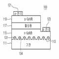
도 1을 참조하면, 질화물 반도체 발광소자는 사파이어 기판(11) 위에 n형 GaN층(15)이 형성되며, 상기 n형 GaN층의 일부에 활성층(17)이 형성되고, 상기 활성층 위에 p형 GaN층(19)이 형성되며, 상기 p형 GaN층 위에 p형 전극(21)이 형성되며, 상기 n형 GaN층(15) 위에 상기 활성층이 형성되지 않는 부분에 n형 전극(23)이 형성된다.Referring to FIG. 1, in the nitride semiconductor light emitting device, an n-
이러한 질화물 반도체 발광소자의 p형 전극(21) 및 n형 전극(23)에 전류를 인가할 때, 활성층(17)에서 생성된 광은 활성층 내부에서 모든 방향으로 방사하게 된다. 이때, 질화물계 반도체들의 굴절률 값이 공기와 발광소자 칩을 둘러싸고 있는 캡 소재인 에폭시의 굴절률에 비해 너무 크기 때문에, 공기 또는 에폭시로 방사되는 경우 어떤 임계 각도보다 작은 각도로 방사되는 광만이 외부로 탈출되고, 상기 임계 각도보다 큰 각도를 갖는 광은 반도체/공기 간의 계면에서 반사하게 되어 반도체 물질 내부로 흡수된다.When current is applied to the p-
이렇게 반도체 내로 흡수되는 광에 의해 발광소자의 외부 발광 효율이 떨어짐과 아울러, 발광소자의 수명에도 악 영향을 미치게 된다. 따라서, 활성층(15)에서 생성된 광 중에서 반도체 물질 내로 반사되는 빛의 양을 최대한 감소시키는 것이 중요하다.As such, the light absorbed into the semiconductor decreases the external light emitting efficiency of the light emitting device and adversely affects the life of the light emitting device. Therefore, it is important to reduce as much as possible the amount of light reflected in the semiconductor material among the light generated in the
또한 사파이어 기판(11)과 n형 GaN층(15)의 경계면(13)에서 사파이어 기판(11)의 굴절률(~1.8)과 n형 GaN층(15)의 굴절률(~2.4)의 차이에 의해서 활성층(17)에서 사파이어 기판(11)쪽으로 발광하는 광이 상기 경계면(13)에서 전반사가 일어나게 되고, 또 p형 전극(21)이나 외부 몰드층의 굴절률 차이에 의해서 다시 반사되어 발광소자의 측면으로 가이딩되다가 빛이 소멸되어 외부 발광 효율이 떨어지게 된다.In addition, the active layer is formed by the difference between the refractive index (˜1.8) of the
본 발명은 질화물 반도체 발광소자를 제공한다.The present invention provides a nitride semiconductor light emitting device.
본 발명은 굴절율이 다른 영역을 갖는 반사 패턴을 형성할 수 있도록 한 질 화물 반도체 발광소자를 제공한다.The present invention provides a nitride semiconductor light emitting device capable of forming a reflective pattern having regions having different refractive indices.
본 발명은 기판 표면에 공극 영역을 갖는 반사 패턴을 제공할 수 있도록 한 질화물 반도체 발광소자를 제공한다.The present invention provides a nitride semiconductor light emitting device capable of providing a reflective pattern having a void region on a substrate surface.
본 발명 실시 예에 의한 질화물 반도체 발광소자는 기판 및 상기 기판 위에 n형 질화물층, 활성층, p형 질화물층을 포함하는 발광 소자에 있어서, 상기 기판 표면에 다수개가 형성된 링 형상의 반사패턴을 포함한다.A nitride semiconductor light emitting device according to an embodiment of the present invention includes a substrate and a ring-shaped reflection pattern in which a plurality of light emitting devices including an n-type nitride layer, an active layer, and a p-type nitride layer are formed on a surface of the substrate. .
본 발명 실시 예에 의한 질화물 반도체 발광소자는, 기판 및 상기 기판 위에 n형 질화물층, 활성층, p형 질화물층을 포함하는 발광 소자에 있어서, 상기 기판 표면에 다수개가 형성되며, 공극 영역을 갖는 반사패턴을 포함한다.A nitride semiconductor light emitting device according to an embodiment of the present invention includes a substrate and a light emitting device including an n-type nitride layer, an active layer, and a p-type nitride layer on the substrate, and a plurality of nitride semiconductor light emitting devices are formed on the surface of the substrate and have reflections having void regions. Contains a pattern.
이하에서 첨부된 도면을 참조하여 본 발명의 실시 예에 따른 질화물 반도체 발광소자에 대하여 상세히 설명한다.Hereinafter, a nitride semiconductor light emitting device according to an embodiment of the present invention will be described in detail with reference to the accompanying drawings.
도 2는 본 발명의 실시 예에 따른 질화물 반도체 발광소자를 나타낸 측 단면도이다.2 is a side cross-sectional view showing a nitride semiconductor light emitting device according to an embodiment of the present invention.
도 2를 참조하면, 질화물 반도체 발광소자(100)는 반사 패턴(131)을 갖는 기판(111), n형 질화물층(115), 활성층(117), p형 질화물층(119), p형 전극(121) 및 n형 전극(123)을 포함한다.Referring to FIG. 2, the nitride semiconductor
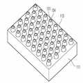
상기 기판(111)은 사파이어 기판, 실리콘 카바이드(SiC), ZnO, Si, GaAs와 GaN 중 어느 하나로 형성될 수 있다. 이러한 기판(111)의 표면(113)에는 다수개의 반사 패턴(131)이 형성되는 데, 상기 반사 패턴(131)은 링 형상(또는 고리, 도너츠 형상 등)으로 돌출된다.The
이러한 링 형상의 반사 패턴(131)의 내부 중앙에는 하나 또는 그 이상의 공극 영역(134)이 형성되는데, 상기 링 형상의 반사 패턴(131)이 원뿔 구조로 연결되어 형성되는 구조이고, 상기 공극 영역(134)이 역 원뿔 구조로 형성될 수 있다. 본 발명은 stripe 구조나 다른 구조에서도 내부에 공극 영역을 형성할 수 있다. 여기서 원뿔 구조의 반사 패턴(131)의 둘레가 반드시 원 형태가 아닐 수도 있다.One or more
이를 위해, 기판(111) 상에 포토 레지스트 패터닝을 수행한 후 마스크 패턴을 형성하고, 상기 마스크 패턴을 식각함으로써 도 3과 같이 링 형상의 반사 패턴(131)이 형성된다. 여기서, 식각 방법으로는 RIE(reactive ion etching) 또는 ICP 에칭(inductive coupled plasma) 등과 같은 건식 식각 방법으로 식각을 수행하게 된다.To this end, a mask pattern is formed after the photoresist patterning is performed on the
이와 같이, 기판 표면(113)에는 링 형상의 반사 패턴(131)이 규칙적인 간격으로 형성되고, 인접한 반사패턴과는 지그재그로 형성될 수도 있다. 또는 기판 표면의 반사패턴을 랜덤하게 형성될 수도 있다.In this manner, ring-shaped
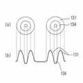
도 4는 본 발명 실시 예에 따른 링 형상의 반사 패턴을 나타낸 정면도 및 측 단면도이다.4 is a front view and a side cross-sectional view showing a ring-shaped reflection pattern according to an exemplary embodiment of the present invention.
도 4를 참조하면, 링 형상의 반사 패턴(131)은 원뿔 형태가 링 형태로 연결되며, 반사 패턴(131)의 중앙에는 역 원뿔 구조의 공극 영역(134)이 형성된다. 이 때 기판 자체의 굴절율, 반사 패턴에서의 굴절율, 공극 영역에서의 굴절율은 서로 다른 값으로 갖는다. 여기서, 공극 영역의 굴절율은 1이 될 수 있다.Referring to FIG. 4, the ring-shaped
도 5는 본 발명 실시 예에 따른 링 형상의 반사 패턴이 형성된 기판 상에 질화물층을 적층한 예이다.5 illustrates an example in which a nitride layer is stacked on a substrate on which a ring-shaped reflective pattern is formed according to an exemplary embodiment of the present invention.
도 5를 참조하면, 기판(111)의 표면에 링 형상의 반사 패턴(131)이 형성되면, 기판 표면에 NH3, TMG, 및 Si와 같은 n형 도펀트를 포함한 실란가스를 공급하여 n형 질화물층(115)을 성장시킨다. 이때 n형 질화물층(115)은 기판 표면, 링 형상의 반사패턴 외측 및 상측으로 성장되며, 상기 반사 패턴 중앙의 공극 영역(134)에는 채워지지 않게 된다. 이는 반사 패턴(131)의 공극 영역(134)이 일정 직경 이하(예: 1~0.5㎛)가 될 때 그 이하로 n형 질화물층(115)이 성장되지 않고 공극 영역(134)으로 남아 있게 된다.Referring to FIG. 5, when the ring-shaped
여기서, 반사 패턴(131)의 링 직경(d2)은 1.5~2㎛ 정도이며, 반사 패턴의 공극 영역(134)의 최소 직경(d1)은 0.5㎛ 또는 그 이하로 형성될 수 있으며, 공극 영역의 최대 직경(d5)은 2㎛ 정도로 형성될 수 있다. 여기서 공극 영역의 최대 직경(d5)은 원뿔 형상의 정점을 직선으로 연결하는 거리 정도이다. 또한 반사 패턴의 직경(d4)은 5㎛ 정도이며, 반사 패턴의 높이(H1)는 1.5~2㎛ 정도이고, 반사 패턴 간의 거리(d3)는 2~3㎛ 정도로 형성될 수 있다. 이러한 반사 패턴 및 공극 영역에서의 직경, 거리, 높이, 간격 등은 공극 영역의 크기, 광 효율 등에 따라 변경할 수도 있다.Here, the ring diameter (d2) of the
이러한 기판 위에는 n형 질화물층을 포함하는 발광 다이오드 구조물이 적층 되는데, 도 2와 같이 발광 다이오드 구조물은 상기 기판(111) 위에 n형 질화물층(115)이 형성되며, 상기 n형 질화물층(115)의 일부에는 단일 또는 다중 양자 우물 구조의 활성층(117)이 형성되며, 상기 활성층 위에는 p형 질화물층(119)이 형성된다. 상기 n형 질화물층(115) 위에서 상기 활성층이 형성되지 않는 부분에 n형 전극(123)이 형성되고, p형 질화물층 위에 p형 전극(121)이 형성된다.A light emitting diode structure including an n-type nitride layer is stacked on the substrate, and as shown in FIG. 2, an n-
본 발명은 GaAs, AlGaAs, GaN, InGaN 및 AlGaInP 등의 화합물 반도체 재료를 이용하는 pn 접합 또는 npn 접합 구조에 적용될 수 있으며, 상기 기판과 n형 질화물층 사이에 한 층 이상의 버퍼층(미도시)이 더 형성될 수도 있다. 이때, 기판 표면에 버퍼층이 형성되더라도, 반사 패턴 내부에는 공극 영역이 존재할 수 있게 된다.The present invention can be applied to a pn junction or npn junction structure using a compound semiconductor material such as GaAs, AlGaAs, GaN, InGaN, and AlGaInP, further comprising one or more buffer layers (not shown) between the substrate and the n-type nitride layer. May be At this time, even if the buffer layer is formed on the substrate surface, the void region may exist inside the reflective pattern.
이러한 질화물 반도체 발광소자(100)는 n형 전극(123) 및 p형 전극(121)을 통해 전류가 인가되면, 활성층(117)에서 광이 생성된다. 상기 생성된 광은 모든 방향으로 방출되는데, 이때 기판 방향으로 방출되는 광은 기판(111)과 n형 질화물층(115) 경계면에 위치한 반사 패턴에 의해 난반사되어 외부로 방출될 수 있고, 또한 상기 방출되는 광이 반사 패턴 내부의 공극 영역에 의해 굴절되어 기판 표면이나 반사 패턴 내부 표면에서 반사되어 외부로 방출될 수 있다.When the current is applied to the nitride semiconductor
이상에서 본 발명에 대하여 실시 예를 중심으로 설명하였으나 이는 단지 예시일 뿐 본 발명을 한정하는 것이 아니며, 본 발명이 속하는 분야의 통상의 지식을 가진 자라면 본 발명의 본질적인 특성을 벗어나지 않는 범위에서 이상에 예시되지 않은 여러 가지의 변형과 응용이 가능함을 알 수 있을 것이다. 예를 들어, 본 발명의 실시예에 구체적으로 나타난 각 구성 요소는 변형하여 실시할 수 있는 것이다. 그리고 이러한 변형과 응용에 관계된 차이점들은 첨부된 청구 범위에서 규정하는 본 발명의 범위에 포함되는 것으로 해석되어야 할 것이다.Although the present invention has been described above with reference to the embodiments, these are only examples and are not intended to limit the present invention, and those skilled in the art to which the present invention pertains may have an abnormality within the scope not departing from the essential characteristics of the present invention. It will be appreciated that various modifications and applications are not illustrated. For example, each component specifically shown in the embodiments of the present invention can be modified and implemented. It is to be understood that all changes and modifications that come within the meaning and range of equivalency of the claims are therefore intended to be embraced therein.
본 발명 실시 예에 따른 질화물 반도체 발광소자에 의하면, 기판 표면에 형성된 반사 패턴에 공극 영역이 형성하여 서로 다른 굴절율을 가지도록 함으로써, 발광소자의 광도를 개선하는 효과가 있다.According to the nitride semiconductor light emitting device according to the embodiment of the present invention, the void region is formed in the reflective pattern formed on the substrate surface to have different refractive indices, thereby improving the brightness of the light emitting device.
Claims (9)
Translated fromKoreanPriority Applications (3)
| Application Number | Priority Date | Filing Date | Title |
|---|---|---|---|
| KR1020070036856AKR101338698B1 (en) | 2007-04-16 | 2007-04-16 | Nitride semiconductor light emitting device |
| US12/103,553US7732802B2 (en) | 2007-04-16 | 2008-04-15 | Semiconductor light emitting device |
| US12/768,713US7915606B2 (en) | 2007-04-16 | 2010-04-27 | Semiconductor light emitting device |
Applications Claiming Priority (1)
| Application Number | Priority Date | Filing Date | Title |
|---|---|---|---|
| KR1020070036856AKR101338698B1 (en) | 2007-04-16 | 2007-04-16 | Nitride semiconductor light emitting device |
Publications (2)
| Publication Number | Publication Date |
|---|---|
| KR20080093222A KR20080093222A (en) | 2008-10-21 |
| KR101338698B1true KR101338698B1 (en) | 2013-12-06 |
Family
ID=39852899
Family Applications (1)
| Application Number | Title | Priority Date | Filing Date |
|---|---|---|---|
| KR1020070036856AExpired - Fee RelatedKR101338698B1 (en) | 2007-04-16 | 2007-04-16 | Nitride semiconductor light emitting device |
Country Status (2)
| Country | Link |
|---|---|
| US (2) | US7732802B2 (en) |
| KR (1) | KR101338698B1 (en) |
Cited By (1)
| Publication number | Priority date | Publication date | Assignee | Title |
|---|---|---|---|---|
| WO2020013563A1 (en)* | 2018-07-09 | 2020-01-16 | 서울바이오시스 주식회사 | Light-emitting element and method for manufacturing same |
Families Citing this family (40)
| Publication number | Priority date | Publication date | Assignee | Title |
|---|---|---|---|---|
| WO2010028146A2 (en)* | 2008-09-08 | 2010-03-11 | 3M Innovative Properties Company | Electrically pixelated luminescent device |
| US8513685B2 (en)* | 2008-11-13 | 2013-08-20 | 3M Innovative Properties Company | Electrically pixelated luminescent device incorporating optical elements |
| KR101055090B1 (en)* | 2009-03-02 | 2011-08-08 | 엘지이노텍 주식회사 | Semiconductor light emitting device and manufacturing method thereof |
| WO2010143778A1 (en) | 2009-06-10 | 2010-12-16 | 서울옵토디바이스주식회사 | Semiconductor substrate, fabrication method thereof, semiconductor device and fabrication method thereof |
| US8481411B2 (en) | 2009-06-10 | 2013-07-09 | Seoul Opto Device Co., Ltd. | Method of manufacturing a semiconductor substrate having a cavity |
| US8860183B2 (en) | 2009-06-10 | 2014-10-14 | Seoul Viosys Co., Ltd. | Semiconductor substrate, semiconductor device, and manufacturing methods thereof |
| JP5847083B2 (en) | 2009-08-26 | 2016-01-20 | ソウル バイオシス カンパニー リミテッドSeoul Viosys Co.,Ltd. | Method for manufacturing light emitting device |
| JP4881492B2 (en)* | 2009-09-17 | 2012-02-22 | 株式会社東芝 | Semiconductor light emitting device |
| KR101125395B1 (en)* | 2009-10-28 | 2012-03-27 | 엘지이노텍 주식회사 | Light emitting device and fabrication method thereof |
| KR101178505B1 (en)* | 2009-11-03 | 2012-09-07 | 주식회사루미지엔테크 | Substrate for semiconductor device and method for manufacturing the same |
| KR101631599B1 (en) | 2009-12-02 | 2016-06-27 | 삼성전자주식회사 | Light Emitting Device and method for manufacturing the same |
| KR101034085B1 (en)* | 2009-12-10 | 2011-05-13 | 엘지이노텍 주식회사 | Light emitting device and manufacturing method |
| KR101277445B1 (en)* | 2009-12-11 | 2013-06-27 | 엘지디스플레이 주식회사 | Semiconductor Light Emitting Device and Method for Manufacturing Thereof |
| US8203153B2 (en) | 2010-01-15 | 2012-06-19 | Koninklijke Philips Electronics N.V. | III-V light emitting device including a light extracting structure |
| KR101028251B1 (en) | 2010-01-19 | 2011-04-11 | 엘지이노텍 주식회사 | Semiconductor light emitting device and manufacturing method thereof |
| JP5570838B2 (en) | 2010-02-10 | 2014-08-13 | ソウル バイオシス カンパニー リミテッド | Semiconductor substrate, manufacturing method thereof, semiconductor device and manufacturing method thereof |
| US8642368B2 (en)* | 2010-03-12 | 2014-02-04 | Applied Materials, Inc. | Enhancement of LED light extraction with in-situ surface roughening |
| CN101807646A (en)* | 2010-03-22 | 2010-08-18 | 徐瑾 | Highly efficient light-emitting diode by using air to form patterned substrate and preparation method thereof |
| US20120049179A1 (en)* | 2010-08-25 | 2012-03-01 | Walsin Lihwa Corporation | Group-iii nitride-based light emitting device having enhanced light extraction efficiency and manufacturing method thereof |
| TW201214802A (en)* | 2010-09-27 | 2012-04-01 | Nat Univ Chung Hsing | Patterned substrate and LED formed using the same |
| CN102194940A (en)* | 2010-11-16 | 2011-09-21 | 华灿光电股份有限公司 | Light-emitting diode (LED) with built-in reflector and preparation method thereof |
| KR101762176B1 (en) | 2010-11-23 | 2017-07-27 | 삼성전자 주식회사 | Nano rod light emitting device |
| TW201232806A (en)* | 2011-01-31 | 2012-08-01 | Walsin Lihwa Corp | Method for fabricating light emitting diode chip |
| CN102651438B (en)* | 2011-02-28 | 2015-05-13 | 比亚迪股份有限公司 | Substrate, preparation method thereof and chip with substrate |
| KR101259999B1 (en)* | 2011-04-28 | 2013-05-06 | 서울옵토디바이스주식회사 | Semiconductor substrate and method of fabricating the same |
| JP5875249B2 (en)* | 2011-04-28 | 2016-03-02 | ソウル バイオシス カンパニー リミテッドSeoul Viosys Co.,Ltd. | Semiconductor substrate, semiconductor device and manufacturing method thereof |
| CN102368526A (en)* | 2011-10-27 | 2012-03-07 | 华灿光电股份有限公司 | Manufacturing method for near ultraviolet LED device |
| TWI528579B (en)* | 2012-04-18 | 2016-04-01 | 新世紀光電股份有限公司 | Light emitting diode device |
| TW201347231A (en)* | 2012-05-04 | 2013-11-16 | Lextar Electronics Corp | Light-emitting diode component |
| KR20130128745A (en)* | 2012-05-17 | 2013-11-27 | 서울바이오시스 주식회사 | Light emitting diode including void in substrate and fabrication method for the same |
| US9000414B2 (en)* | 2012-11-16 | 2015-04-07 | Korea Photonics Technology Institute | Light emitting diode having heterogeneous protrusion structures |
| US20140159182A1 (en)* | 2012-12-06 | 2014-06-12 | ThinSillicon Corporation | Semiconductor device and method for manufacturing a semiconductor device having an undulating reflective surface of an electrode |
| TWI604632B (en) | 2013-04-25 | 2017-11-01 | 晶元光電股份有限公司 | Light-emitting diode device |
| CN104425661B (en)* | 2013-08-22 | 2017-03-01 | 展晶科技(深圳)有限公司 | Light-emitting diode and its manufacturing method |
| CN103887390B (en)* | 2014-01-29 | 2017-06-27 | 华灿光电(苏州)有限公司 | Patterned sapphire substrate, manufacturing method thereof, and epitaxial wafer manufacturing method |
| US9548419B2 (en) | 2014-05-20 | 2017-01-17 | Southern Taiwan University Of Science And Technology | Light emitting diode chip having multi microstructure substrate surface |
| KR102369976B1 (en)* | 2015-07-16 | 2022-03-04 | 쑤저우 레킨 세미컨덕터 컴퍼니 리미티드 | Light emittng device |
| KR102573271B1 (en)* | 2018-04-27 | 2023-08-31 | 삼성전자주식회사 | Semiconductor light emitting device |
| CN109346580B (en)* | 2018-08-28 | 2020-03-27 | 华灿光电(浙江)有限公司 | A kind of manufacturing method of light-emitting diode epitaxial wafer |
| CN115394886A (en)* | 2022-09-29 | 2022-11-25 | 福建晶安光电有限公司 | Patterned substrate, preparation method thereof and LED chip |
Citations (4)
| Publication number | Priority date | Publication date | Assignee | Title |
|---|---|---|---|---|
| JP2001274093A (en) | 2000-03-24 | 2001-10-05 | Mitsubishi Cable Ind Ltd | Semiconductor base and its manufacturing method |
| KR20060135568A (en)* | 2005-06-25 | 2006-12-29 | (주)에피플러스 | Semiconductor light-emitting device with improved brightness and manufacturing method thereof |
| WO2007001141A1 (en) | 2005-06-25 | 2007-01-04 | Epiplus Co., Ltd. | Semiconductor light emitting device having improved luminance and method thereof |
| KR20070097640A (en)* | 2006-03-28 | 2007-10-05 | 전북대학교산학협력단 | Method of manufacturing a semiconductor structure |
Family Cites Families (3)
| Publication number | Priority date | Publication date | Assignee | Title |
|---|---|---|---|---|
| US4638334A (en)* | 1985-04-03 | 1987-01-20 | Xerox Corporation | Electro-optic line printer with super luminescent LED source |
| US20070267646A1 (en)* | 2004-06-03 | 2007-11-22 | Philips Lumileds Lighting Company, Llc | Light Emitting Device Including a Photonic Crystal and a Luminescent Ceramic |
| US7483466B2 (en)* | 2005-04-28 | 2009-01-27 | Canon Kabushiki Kaisha | Vertical cavity surface emitting laser device |
- 2007
- 2007-04-16KRKR1020070036856Apatent/KR101338698B1/ennot_activeExpired - Fee Related
- 2008
- 2008-04-15USUS12/103,553patent/US7732802B2/enactiveActive
- 2010
- 2010-04-27USUS12/768,713patent/US7915606B2/enactiveActive
Patent Citations (4)
| Publication number | Priority date | Publication date | Assignee | Title |
|---|---|---|---|---|
| JP2001274093A (en) | 2000-03-24 | 2001-10-05 | Mitsubishi Cable Ind Ltd | Semiconductor base and its manufacturing method |
| KR20060135568A (en)* | 2005-06-25 | 2006-12-29 | (주)에피플러스 | Semiconductor light-emitting device with improved brightness and manufacturing method thereof |
| WO2007001141A1 (en) | 2005-06-25 | 2007-01-04 | Epiplus Co., Ltd. | Semiconductor light emitting device having improved luminance and method thereof |
| KR20070097640A (en)* | 2006-03-28 | 2007-10-05 | 전북대학교산학협력단 | Method of manufacturing a semiconductor structure |
Cited By (5)
| Publication number | Priority date | Publication date | Assignee | Title |
|---|---|---|---|---|
| WO2020013563A1 (en)* | 2018-07-09 | 2020-01-16 | 서울바이오시스 주식회사 | Light-emitting element and method for manufacturing same |
| JP2021530856A (en)* | 2018-07-09 | 2021-11-11 | ソウル バイオシス カンパニー リミテッドSeoul Viosys Co., Ltd. | Light emitting device and its manufacturing method |
| US11658264B2 (en) | 2018-07-09 | 2023-05-23 | Seoul Viosys Co., Ltd. | Light emitting device having a substrate with a pattern of protrusions and manufacturing method thereof |
| JP7436371B2 (en) | 2018-07-09 | 2024-02-21 | ソウル バイオシス カンパニー リミテッド | light emitting device |
| US12176458B2 (en) | 2018-07-09 | 2024-12-24 | Seoul Viosys Co., Ltd. | Light emitting device and manufacturing method thereof |
Also Published As
| Publication number | Publication date |
|---|---|
| KR20080093222A (en) | 2008-10-21 |
| US20100207155A1 (en) | 2010-08-19 |
| US7915606B2 (en) | 2011-03-29 |
| US20080251803A1 (en) | 2008-10-16 |
| US7732802B2 (en) | 2010-06-08 |
Similar Documents
| Publication | Publication Date | Title |
|---|---|---|
| KR101338698B1 (en) | Nitride semiconductor light emitting device | |
| KR101148706B1 (en) | Semiconductor light-emitting device | |
| US9929327B2 (en) | Light-emitting device package and light-emitting module including the same | |
| CN102074633B (en) | Luminescent device, light emitting device package and illuminator | |
| CN102122694A (en) | Light emitting diode having electrode pads | |
| US20130045556A1 (en) | Light-Emitting Devices with Textured Active Layer | |
| CN102169939A (en) | Light emitting device, light emitting device package, and lighting system | |
| JP2006339627A (en) | Vertical structure nitride semiconductor light emitting diode | |
| CN107689407A (en) | A kind of LED chip and preparation method thereof | |
| KR101039880B1 (en) | Light emitting device and light emitting device package | |
| KR102261727B1 (en) | Light emitting device and light emitting device package including the same | |
| TW201624767A (en) | Light-emitting diode containing porous transparent electrode | |
| KR20080026883A (en) | Nitride Semiconductor Light Emitting Device | |
| KR101321356B1 (en) | Nitride semiconductor light emitting device | |
| KR20200034425A (en) | Light emitting device and backlight unit including the same | |
| KR20150083248A (en) | Package for light emitting device | |
| KR20170124281A (en) | Light emitting device package | |
| KR20160016236A (en) | Light emitting device and lighting system | |
| JP2019145819A (en) | Light emitting device and light emitting device package | |
| KR101462464B1 (en) | Light emitting diode with donut-shaped hole array | |
| KR101435512B1 (en) | Light emitting diode having mixed structure | |
| TWI706578B (en) | Micro light emitting diode chip | |
| KR20110117856A (en) | Light emitting diode device and manufacturing method thereof | |
| US20070096120A1 (en) | Lateral current GaN flip chip LED with shaped transparent substrate | |
| KR20190038105A (en) | Light emitting device package and method of manufacturing the same |
Legal Events
| Date | Code | Title | Description |
|---|---|---|---|
| PA0109 | Patent application | St.27 status event code:A-0-1-A10-A12-nap-PA0109 | |
| PG1501 | Laying open of application | St.27 status event code:A-1-1-Q10-Q12-nap-PG1501 | |
| P22-X000 | Classification modified | St.27 status event code:A-2-2-P10-P22-nap-X000 | |
| R17-X000 | Change to representative recorded | St.27 status event code:A-3-3-R10-R17-oth-X000 | |
| PN2301 | Change of applicant | St.27 status event code:A-3-3-R10-R13-asn-PN2301 St.27 status event code:A-3-3-R10-R11-asn-PN2301 | |
| R18-X000 | Changes to party contact information recorded | St.27 status event code:A-3-3-R10-R18-oth-X000 | |
| A201 | Request for examination | ||
| PA0201 | Request for examination | St.27 status event code:A-1-2-D10-D11-exm-PA0201 | |
| D13-X000 | Search requested | St.27 status event code:A-1-2-D10-D13-srh-X000 | |
| D14-X000 | Search report completed | St.27 status event code:A-1-2-D10-D14-srh-X000 | |
| E902 | Notification of reason for refusal | ||
| PE0902 | Notice of grounds for rejection | St.27 status event code:A-1-2-D10-D21-exm-PE0902 | |
| P11-X000 | Amendment of application requested | St.27 status event code:A-2-2-P10-P11-nap-X000 | |
| P13-X000 | Application amended | St.27 status event code:A-2-2-P10-P13-nap-X000 | |
| P22-X000 | Classification modified | St.27 status event code:A-2-2-P10-P22-nap-X000 | |
| E701 | Decision to grant or registration of patent right | ||
| PE0701 | Decision of registration | St.27 status event code:A-1-2-D10-D22-exm-PE0701 | |
| GRNT | Written decision to grant | ||
| PR0701 | Registration of establishment | St.27 status event code:A-2-4-F10-F11-exm-PR0701 | |
| PR1002 | Payment of registration fee | St.27 status event code:A-2-2-U10-U11-oth-PR1002 Fee payment year number:1 | |
| PG1601 | Publication of registration | St.27 status event code:A-4-4-Q10-Q13-nap-PG1601 | |
| PN2301 | Change of applicant | St.27 status event code:A-5-5-R10-R13-asn-PN2301 St.27 status event code:A-5-5-R10-R11-asn-PN2301 | |
| FPAY | Annual fee payment | Payment date:20161104 Year of fee payment:4 | |
| PR1001 | Payment of annual fee | St.27 status event code:A-4-4-U10-U11-oth-PR1001 Fee payment year number:4 | |
| R18-X000 | Changes to party contact information recorded | St.27 status event code:A-5-5-R10-R18-oth-X000 | |
| FPAY | Annual fee payment | Payment date:20171107 Year of fee payment:5 | |
| PR1001 | Payment of annual fee | St.27 status event code:A-4-4-U10-U11-oth-PR1001 Fee payment year number:5 | |
| R18-X000 | Changes to party contact information recorded | St.27 status event code:A-5-5-R10-R18-oth-X000 | |
| FPAY | Annual fee payment | Payment date:20181112 Year of fee payment:6 | |
| PR1001 | Payment of annual fee | St.27 status event code:A-4-4-U10-U11-oth-PR1001 Fee payment year number:6 | |
| FPAY | Annual fee payment | Payment date:20191111 Year of fee payment:7 | |
| PR1001 | Payment of annual fee | St.27 status event code:A-4-4-U10-U11-oth-PR1001 Fee payment year number:7 | |
| R18-X000 | Changes to party contact information recorded | St.27 status event code:A-5-5-R10-R18-oth-X000 | |
| PR1001 | Payment of annual fee | St.27 status event code:A-4-4-U10-U11-oth-PR1001 Fee payment year number:8 | |
| PN2301 | Change of applicant | St.27 status event code:A-5-5-R10-R13-asn-PN2301 St.27 status event code:A-5-5-R10-R11-asn-PN2301 | |
| PN2301 | Change of applicant | St.27 status event code:A-5-5-R10-R11-asn-PN2301 | |
| PN2301 | Change of applicant | St.27 status event code:A-5-5-R10-R14-asn-PN2301 | |
| PR1001 | Payment of annual fee | St.27 status event code:A-4-4-U10-U11-oth-PR1001 Fee payment year number:9 | |
| PR1001 | Payment of annual fee | St.27 status event code:A-4-4-U10-U11-oth-PR1001 Fee payment year number:10 | |
| PR1001 | Payment of annual fee | St.27 status event code:A-4-4-U10-U11-oth-PR1001 Fee payment year number:11 | |
| PC1903 | Unpaid annual fee | St.27 status event code:A-4-4-U10-U13-oth-PC1903 Not in force date:20241203 Payment event data comment text:Termination Category : DEFAULT_OF_REGISTRATION_FEE | |
| P22-X000 | Classification modified | St.27 status event code:A-4-4-P10-P22-nap-X000 | |
| PC1903 | Unpaid annual fee | St.27 status event code:N-4-6-H10-H13-oth-PC1903 Ip right cessation event data comment text:Termination Category : DEFAULT_OF_REGISTRATION_FEE Not in force date:20241203 |