KR101335527B1 - Organic Light Emitting Diode Display Device and Method for Manufacturing The Same - Google Patents
Organic Light Emitting Diode Display Device and Method for Manufacturing The SameDownload PDFInfo
- Publication number
- KR101335527B1 KR101335527B1KR1020120018612AKR20120018612AKR101335527B1KR 101335527 B1KR101335527 B1KR 101335527B1KR 1020120018612 AKR1020120018612 AKR 1020120018612AKR 20120018612 AKR20120018612 AKR 20120018612AKR 101335527 B1KR101335527 B1KR 101335527B1
- Authority
- KR
- South Korea
- Prior art keywords
- electrode
- metal layer
- layer
- contact hole
- drain
- Prior art date
- Legal status (The legal status is an assumption and is not a legal conclusion. Google has not performed a legal analysis and makes no representation as to the accuracy of the status listed.)
- Active
Links
Images


Classifications
- H—ELECTRICITY
- H10—SEMICONDUCTOR DEVICES; ELECTRIC SOLID-STATE DEVICES NOT OTHERWISE PROVIDED FOR
- H10D—INORGANIC ELECTRIC SEMICONDUCTOR DEVICES
- H10D86/00—Integrated devices formed in or on insulating or conducting substrates, e.g. formed in silicon-on-insulator [SOI] substrates or on stainless steel or glass substrates
- H10D86/40—Integrated devices formed in or on insulating or conducting substrates, e.g. formed in silicon-on-insulator [SOI] substrates or on stainless steel or glass substrates characterised by multiple TFTs
- H10D86/481—Integrated devices formed in or on insulating or conducting substrates, e.g. formed in silicon-on-insulator [SOI] substrates or on stainless steel or glass substrates characterised by multiple TFTs integrated with passive devices, e.g. auxiliary capacitors
- G—PHYSICS
- G09—EDUCATION; CRYPTOGRAPHY; DISPLAY; ADVERTISING; SEALS
- G09G—ARRANGEMENTS OR CIRCUITS FOR CONTROL OF INDICATING DEVICES USING STATIC MEANS TO PRESENT VARIABLE INFORMATION
- G09G3/00—Control arrangements or circuits, of interest only in connection with visual indicators other than cathode-ray tubes
- G09G3/20—Control arrangements or circuits, of interest only in connection with visual indicators other than cathode-ray tubes for presentation of an assembly of a number of characters, e.g. a page, by composing the assembly by combination of individual elements arranged in a matrix no fixed position being assigned to or needed to be assigned to the individual characters or partial characters
- G09G3/34—Control arrangements or circuits, of interest only in connection with visual indicators other than cathode-ray tubes for presentation of an assembly of a number of characters, e.g. a page, by composing the assembly by combination of individual elements arranged in a matrix no fixed position being assigned to or needed to be assigned to the individual characters or partial characters by control of light from an independent source
- G09G3/36—Control arrangements or circuits, of interest only in connection with visual indicators other than cathode-ray tubes for presentation of an assembly of a number of characters, e.g. a page, by composing the assembly by combination of individual elements arranged in a matrix no fixed position being assigned to or needed to be assigned to the individual characters or partial characters by control of light from an independent source using liquid crystals
- G09G3/3611—Control of matrices with row and column drivers
- G09G3/3648—Control of matrices with row and column drivers using an active matrix
- G09G3/3655—Details of drivers for counter electrodes, e.g. common electrodes for pixel capacitors or supplementary storage capacitors
- H—ELECTRICITY
- H10—SEMICONDUCTOR DEVICES; ELECTRIC SOLID-STATE DEVICES NOT OTHERWISE PROVIDED FOR
- H10D—INORGANIC ELECTRIC SEMICONDUCTOR DEVICES
- H10D86/00—Integrated devices formed in or on insulating or conducting substrates, e.g. formed in silicon-on-insulator [SOI] substrates or on stainless steel or glass substrates
- H10D86/01—Manufacture or treatment
- H10D86/021—Manufacture or treatment of multiple TFTs
- H—ELECTRICITY
- H10—SEMICONDUCTOR DEVICES; ELECTRIC SOLID-STATE DEVICES NOT OTHERWISE PROVIDED FOR
- H10D—INORGANIC ELECTRIC SEMICONDUCTOR DEVICES
- H10D86/00—Integrated devices formed in or on insulating or conducting substrates, e.g. formed in silicon-on-insulator [SOI] substrates or on stainless steel or glass substrates
- H10D86/40—Integrated devices formed in or on insulating or conducting substrates, e.g. formed in silicon-on-insulator [SOI] substrates or on stainless steel or glass substrates characterised by multiple TFTs
- H10D86/60—Integrated devices formed in or on insulating or conducting substrates, e.g. formed in silicon-on-insulator [SOI] substrates or on stainless steel or glass substrates characterised by multiple TFTs wherein the TFTs are in active matrices
- H—ELECTRICITY
- H10—SEMICONDUCTOR DEVICES; ELECTRIC SOLID-STATE DEVICES NOT OTHERWISE PROVIDED FOR
- H10K—ORGANIC ELECTRIC SOLID-STATE DEVICES
- H10K50/00—Organic light-emitting devices
- G—PHYSICS
- G09—EDUCATION; CRYPTOGRAPHY; DISPLAY; ADVERTISING; SEALS
- G09G—ARRANGEMENTS OR CIRCUITS FOR CONTROL OF INDICATING DEVICES USING STATIC MEANS TO PRESENT VARIABLE INFORMATION
- G09G2300/00—Aspects of the constitution of display devices
- G09G2300/04—Structural and physical details of display devices
- G09G2300/0421—Structural details of the set of electrodes
- G09G2300/0426—Layout of electrodes and connections
- G—PHYSICS
- G09—EDUCATION; CRYPTOGRAPHY; DISPLAY; ADVERTISING; SEALS
- G09G—ARRANGEMENTS OR CIRCUITS FOR CONTROL OF INDICATING DEVICES USING STATIC MEANS TO PRESENT VARIABLE INFORMATION
- G09G2300/00—Aspects of the constitution of display devices
- G09G2300/08—Active matrix structure, i.e. with use of active elements, inclusive of non-linear two terminal elements, in the pixels together with light emitting or modulating elements
- G09G2300/0809—Several active elements per pixel in active matrix panels
- G09G2300/0842—Several active elements per pixel in active matrix panels forming a memory circuit, e.g. a dynamic memory with one capacitor
- G09G2300/0847—Several active elements per pixel in active matrix panels forming a memory circuit, e.g. a dynamic memory with one capacitor being a dynamic memory without any storage capacitor, i.e. with use of parasitic capacitances as storage elements
- G—PHYSICS
- G09—EDUCATION; CRYPTOGRAPHY; DISPLAY; ADVERTISING; SEALS
- G09G—ARRANGEMENTS OR CIRCUITS FOR CONTROL OF INDICATING DEVICES USING STATIC MEANS TO PRESENT VARIABLE INFORMATION
- G09G3/00—Control arrangements or circuits, of interest only in connection with visual indicators other than cathode-ray tubes
- G09G3/20—Control arrangements or circuits, of interest only in connection with visual indicators other than cathode-ray tubes for presentation of an assembly of a number of characters, e.g. a page, by composing the assembly by combination of individual elements arranged in a matrix no fixed position being assigned to or needed to be assigned to the individual characters or partial characters
- G09G3/22—Control arrangements or circuits, of interest only in connection with visual indicators other than cathode-ray tubes for presentation of an assembly of a number of characters, e.g. a page, by composing the assembly by combination of individual elements arranged in a matrix no fixed position being assigned to or needed to be assigned to the individual characters or partial characters using controlled light sources
- G09G3/30—Control arrangements or circuits, of interest only in connection with visual indicators other than cathode-ray tubes for presentation of an assembly of a number of characters, e.g. a page, by composing the assembly by combination of individual elements arranged in a matrix no fixed position being assigned to or needed to be assigned to the individual characters or partial characters using controlled light sources using electroluminescent panels
- G09G3/32—Control arrangements or circuits, of interest only in connection with visual indicators other than cathode-ray tubes for presentation of an assembly of a number of characters, e.g. a page, by composing the assembly by combination of individual elements arranged in a matrix no fixed position being assigned to or needed to be assigned to the individual characters or partial characters using controlled light sources using electroluminescent panels semiconductive, e.g. using light-emitting diodes [LED]
- G09G3/3208—Control arrangements or circuits, of interest only in connection with visual indicators other than cathode-ray tubes for presentation of an assembly of a number of characters, e.g. a page, by composing the assembly by combination of individual elements arranged in a matrix no fixed position being assigned to or needed to be assigned to the individual characters or partial characters using controlled light sources using electroluminescent panels semiconductive, e.g. using light-emitting diodes [LED] organic, e.g. using organic light-emitting diodes [OLED]
- H—ELECTRICITY
- H01—ELECTRIC ELEMENTS
- H01L—SEMICONDUCTOR DEVICES NOT COVERED BY CLASS H10
- H01L2924/00—Indexing scheme for arrangements or methods for connecting or disconnecting semiconductor or solid-state bodies as covered by H01L24/00
- H01L2924/01—Chemical elements
- H01L2924/01013—Aluminum [Al]
- H—ELECTRICITY
- H01—ELECTRIC ELEMENTS
- H01L—SEMICONDUCTOR DEVICES NOT COVERED BY CLASS H10
- H01L2924/00—Indexing scheme for arrangements or methods for connecting or disconnecting semiconductor or solid-state bodies as covered by H01L24/00
- H01L2924/01—Chemical elements
- H01L2924/01029—Copper [Cu]
- H—ELECTRICITY
- H01—ELECTRIC ELEMENTS
- H01L—SEMICONDUCTOR DEVICES NOT COVERED BY CLASS H10
- H01L2924/00—Indexing scheme for arrangements or methods for connecting or disconnecting semiconductor or solid-state bodies as covered by H01L24/00
- H01L2924/01—Chemical elements
- H01L2924/01042—Molybdenum [Mo]
Landscapes
- Engineering & Computer Science (AREA)
- Physics & Mathematics (AREA)
- Computer Hardware Design (AREA)
- General Physics & Mathematics (AREA)
- Theoretical Computer Science (AREA)
- Power Engineering (AREA)
- Chemical & Material Sciences (AREA)
- Crystallography & Structural Chemistry (AREA)
- Optics & Photonics (AREA)
- Electroluminescent Light Sources (AREA)
- Devices For Indicating Variable Information By Combining Individual Elements (AREA)
Abstract
Translated fromKoreanDescription
Translated fromKorean본 발명은 유기전계발광표시장치 및 그 제조 방법에 관한 것으로서, 보다 구체적으로 대면적에서 고해상도를 구현할 수 있는 유기전계발광표시장치 및 그 제조방법에 관한 것이다.
The present invention relates to an organic light emitting display device and a manufacturing method thereof, and more particularly, to an organic light emitting display device and a method of manufacturing the same that can realize a high resolution in a large area.
최근 들어 부피와 무게가 큰 음극선관(Cathode Ray Tube)를 대신하여 액정표시장치(Liquid Crystal Display Device)나 유기전계발광표시장치(Organic Light Emitting Diode Display Device)와 같은 평판디스플레이장치의 개발이 활발히 진행되고 있다.Recently, development of flat panel display devices such as liquid crystal display devices and organic light emitting diode display devices instead of cathode ray tubes, which have a large volume and weight, has been actively developed. It is becoming.
이 중 유기전계발광표시장치는 액정표시장치와 달리 별도의 광원이 필요없는 자발광소자이기 때문에 액정표시장치에 비해 두께가 더 얇아지고 무게가 더 가벼우며 색재현율이 액정표시장치에 비해 우수하여 차세대 디스플레이로 각광을 받고 있다.Among them, organic light emitting display devices are self-light emitting devices that do not require a separate light source, unlike liquid crystal displays, and thus are thinner, lighter in weight, and have better color reproduction than liquid crystal displays. The display is in the spotlight.
이와 같은 유기전계발광표시장치는 일반적으로 수동형(Passive type)과 능동형(Active type)으로 나눌 수 있다. 이 중에서 각 화소마다 별도의 박막 트랜지스터(thin film transistor)를 구비하여 소비전력이 낮고 해상도면에서 유리한 이점을 갖고 있는 능동형 유기전계발광표시장치가 고해상도 대면적 화상표시소자를 구현하는데 많이 사용하고 있는 추세이다.Such an organic light emitting display device is generally classified into a passive type and an active type. Among them, an active organic light emitting display device having a low power consumption and an advantage in terms of resolution because of having a separate thin film transistor for each pixel has been widely used to realize a high resolution large area image display device. to be.
도 1은 일반적인 능동형 유기전계발광표시장치(이하 유기전계발광표시장치) 의 단면도이다.1 is a cross-sectional view of a general active organic light emitting display device (hereinafter referred to as an organic light emitting display device).
도 1을 참조하면, 일반적인 유기전계발광표시장치는 기판(substrate, 100) 상에 반도체층(semiconductor layer, 101) 및 제 1 스토리지 전극(storage electrode, 102)이 형성되어 있고, 상부에 복수의 절연막(insulating layer, 110, 120, 130, 140)을 사이에 두고 게이트 전극(gate electrode, 111), 소스 전극(source electrode, 121), 드레인 전극(drain electrode, 122), 제 2 스토리지 전극(112) 및 제 3 스토리지 전극(123)이 형성되어 있다.Referring to FIG. 1, in a typical organic light emitting display device, a
여기서, 제 3 절연막(130) 하부에는 스위칭 트랜지스터(미도시)의 게이트 전극(미도시)과 연결되어 있는 게이트 패드(gate pad, 124) 및 스위칭 트랜지스터의 소스 전극(미도시)과 연결되어 있는 데이터 패드(data pad, 125)가 각각 형성되어 있다. 상기 스위칭 트랜지스터는 본 발명과 직접적으로 관련이 없는 부분으로, 도면에서의 도시는 생략하기로 한다.The
또한, 제 2 절연막(120) 상부에는 소스 전극(121) 및 드레인 전극(122)이 형성되어 있고, 드레인 전극(122)은 애노드 전극(anode, 141)에 연결되어 있다. 유기발광층(organic light emitting layer, 151)은 제 4 절연막(140) 상부에 연장 형성된 애노드 전극(141) 및 뱅크층(bank layer, 150) 상에 형성되어 있다.In addition, a
여기서, 제 1 스토리지 전극(102)과 대응되는 제 1 절연막(110) 상에 제 2 스토리지 전극(112)이 형성되고, 마찬가지로 제 2 스토리지 전극(112)과 대응되는 제 2 절연막(120) 상에 제 3 스토리지 전극(123)이 형성된다. 상기 복수의 스토리지 전극(102, 112, 123)은 정전용량을 발생시켜 게이트 신호가 인가되지 않을 때에도 유기발광층의(151) 발광을 유지시켜주는 역할을 한다. 이러한 복수의 스토리지 전극(102, 112, 123)을 많이 형성할수록 유기발광층(151)을 구동하는데 충분한 정전용량을 확보할 수 있지만, 각 화소 영역의 크기가 제한되어 있기 때문에 제한된 화소 영역에서 고집적도를 통해 고해상도를 구현하기 위해서는 스토리지 전극이 차지하는 면적을 줄이는 회로 설계가 필수적이다.Here, the
한편, 대면적 패널을 구현할 때, 전원공급단에서 멀리 떨어진 화소의 경우 전압강하 현상이 발생하는데, 떨어진 전압을 보상하지 않으면, 휘도 불균일 현상이 발생할 수 있다. 그러나, 각 픽셀의 면적은 동일하게 한정되어 있으며, 상기와 같이 스토리지 전극부를 포함한 보상회로의 구성요소가 많아지면 집적도가 떨어지며, 고해상도 구현이 어렵다.On the other hand, when implementing a large area panel, a voltage drop occurs in the case of pixels far from the power supply terminal. If the dropped voltage is not compensated for, a luminance unevenness may occur. However, the area of each pixel is equally limited, and as the components of the compensation circuit including the storage electrode unit increase as described above, the degree of integration decreases, and high resolution is difficult.
또한, 제 3 콘택홀(140a)은 2개의 층이 식각되어 형성되며, 특히, 평탄화를 위해 형성되는 제 4절연막(140)의 높이가 높기 때문에, 제 4절연막(140) 상에 형성되는 3 콘택홀(140a)의 단차는 다른 콘택홀에 비해 높게 형성된다. 단차가 높은 제 3 콘택홀(140a) 상에 형성되는 애노드 전극(141)은 그 두께가 불균일하게 형성되거나 부분적으로 끊어질 수 있으며, 이는 추후 전기적 연결에 문제를 발생시킬 수 있다.In addition, the
덧붙여, 게이트 패드(124) 및 데이터 패드(125)는 제 4 콘택홀(140b) 및 제 5 콘택홀(140c)이 형성된 후 외부로 노출되는데, 이 부분이 상부에 막이 형성되기 전까지 장시간 외부에 노출되면 산화되어 손상을 입을 수 있다. 이 패드부가 손상되면 전기적 연결이 불안정해질 수 있다.In addition, the
한편, 상기 복수의 스토리지 전극(102, 112, 123) 중에서, 제 2 스토리지 전극(112) 및 제 3 스토리지 전극(123)은 금속으로 형성되지만, 제 1 스토리지 전극(102)은 반도체층(101)과 동일한 물질인 실리콘 계열의 물질로 형성된다. 따라서, 제 1 스토리지 전극(102)을 전극으로 활용하기 위해서는 도핑(doping)공정이라는 별도의 반도체 공정이 추가로 필요하며, 이에 따라 공정의 효율성이 떨어진다.
이와 유사한 기술로써 본 발명의 배경이 되는 기술은 한국 공개특허공보 제10-2006-0001402호(2006.01.06.)에 개시되어 있다.
Meanwhile, the
As a similar technique, the background of the present invention is disclosed in Korean Patent Laid-Open No. 10-2006-0001402 (January 6, 2006).
본 발명은 상술한 문제점을 해결하기 위한 것으로서, 새로운 금속층을 형성하여 고해상도를 구현하고, 대면적에서 휘도 균일도를 향상시키면서 전기적 연결의 안정성을 높이며, 공정의 효율성을 향상시키는 것을 그 기술적 과제로 한다.
SUMMARY OF THE INVENTION The present invention has been made in view of the above-described problems, and provides a high resolution by forming a new metal layer, improves the stability of electrical connection while improving luminance uniformity at large areas, and improves the efficiency of the process.
상술한 목적을 달성하기 위한 본 발명의 일 측면에 따른 유기전계발광표시장치는 기판 상에 형성되고 소스 영역 및 드레인 영역을 포함하는 반도체층; 상기 반도체층 상에 제 1 절연막을 사이에 두고 형성된 게이트 전극 및 제 1 스토리지 전극; 상기 게이트 전극 및 상기 제 1 스토리지 전극 상에 형성된 제 2 절연막; 상기 소스 영역 및 상기 드레인 영역을 노출하는 컨택홀에 각각 형성된 소스 전극 및 드레인 전극; 상기 제 1 스토리지 전극과 대응되는 제 2 절연막 상에 형성된 제 2 스토리지 전극; 상기 소스 전극, 상기 드레인 전극 및 상기 제 2 스토리지 전극 상에 형성된 제 3 절연막; 제 3 절연막이 패터닝되어 외부로 노출된 상기 드레인 전극과 애노드 전극을 연결하는 제 1 금속층; 및 상기 제 2 스토리지 전극과 대응되는 상기 제 3 스토리지 상에 형성된 제 2 금속층을 포함한다.According to an aspect of the present invention, an organic light emitting display device includes: a semiconductor layer formed on a substrate and including a source region and a drain region; A gate electrode and a first storage electrode formed on the semiconductor layer with a first insulating film interposed therebetween; A second insulating film formed on the gate electrode and the first storage electrode; A source electrode and a drain electrode respectively formed in the contact hole exposing the source region and the drain region; A second storage electrode formed on a second insulating layer corresponding to the first storage electrode; A third insulating film formed on the source electrode, the drain electrode and the second storage electrode; A first metal layer patterning a third insulating film to connect the drain electrode and the anode electrode exposed to the outside; And a second metal layer formed on the third storage corresponding to the second storage electrode.
상술한 목적을 달성하기 위한 본 발명의 또 다른 측면에 따른 유기전계발광표시장치 제조방법은 기판 상에 소스 영역과 드레인 영역을 포함하는 반도체층 및 제 1 절연막을 순차적으로 형성하는 단계; 상기 제 1 절연막 상에 게이트 전극 및 제 1 스토리지 전극을 형성하는 단계; 상기 게이트 전극 및 제 1 스토리지 전극 상에 제 2 절연막을 형성하고, 상기 제 2 절연막을 패터닝하여 상기 반도체층의 상기 소스 영역 및 상기 드레인 영역을 각각 노출시키는 컨택홀을 형성하는 단계; 상기 컨택홀에 소스 전극 및 드레인 전극을 형성하는 동시에 상기 제 1 스토리지 전극과 대응되는 상기 제 2 절연막 상에 제 2 스토리지 전극을 형성하는 단계; 상기 소스 전극, 상기 드레인 전극 및 상기 제 2 스토리지 전극 상에 제 3 절연막을 형성하는 단계; 제 3 절연막을 패터닝하여 노출된 상기 드레인 전극 상에 제 1 금속층을 형성하는 단계; 및 상기 제 2 스토리지 전극과 대응되는 상기 제 3 절연막 상에 제 2 금속층을 형성하는 단계를 포함한다.
According to still another aspect of the present invention, there is provided a method of manufacturing an organic light emitting display device, the method including: sequentially forming a semiconductor layer including a source region and a drain region and a first insulating layer on a substrate; Forming a gate electrode and a first storage electrode on the first insulating film; Forming a second insulating film on the gate electrode and the first storage electrode, and forming a contact hole to expose the source region and the drain region of the semiconductor layer by patterning the second insulating layer; Forming a source electrode and a drain electrode in the contact hole and simultaneously forming a second storage electrode on the second insulating layer corresponding to the first storage electrode; Forming a third insulating film on the source electrode, the drain electrode, and the second storage electrode; Patterning a third insulating film to form a first metal layer on the exposed drain electrode; And forming a second metal layer on the third insulating layer corresponding to the second storage electrode.
본 발명에 따르면, 스토리지 전극을 새로운 금속층으로 대체함으로써, 설계의 자유도를 확보하여 고집적화를 통한 고해상도 구현에 유리한 효과가 있다.According to the present invention, by replacing the storage electrode with a new metal layer, there is an advantageous effect to achieve high resolution through high integration by securing the freedom of design.
또한, 본 발명에 따르면, 새로운 금속층과 애노드 전극이 연결되는 전원부를 메쉬(Mesh)구조로 형성하여, 소형뿐만 아니라 대형 패널에서도 휘도 균일도가 향상되는 효과가 있다.In addition, according to the present invention, the power supply unit to which the new metal layer and the anode electrode are connected has a mesh structure, thereby improving luminance uniformity in a small panel as well as a large panel.
또한, 본 발명에 따르면 새로운 금속층이 애노드 전극의 콘택부 단차를 낮춰 전기적 연결의 안정성을 높일 수 있는 효과가 있다.In addition, according to the present invention has a new metal layer has the effect of increasing the stability of the electrical connection by lowering the contact step difference of the anode electrode.
또한, 본 발명에 따르면 별도의 도핑 공정에 의해 형성되는 스토리지 전극을 새로운 금속층으로 대체하여, 공정의 효율성을 향상시킬 수 있는 효과가 있다.
In addition, according to the present invention by replacing the storage electrode formed by a separate doping process with a new metal layer, there is an effect that can improve the efficiency of the process.
도 1은 일반적인 유기전계발광표시장치의 구조를 나타내는 단면도;
도 2는 본 발명의 일 실시예에 따른 유기전계발광표시장치의 구조를 보여주는 단면도;
도 3은 본 발명의 다른 실시예에 따른 유기전계발광표시장치의 구조를 보여주는 단면도;
도 4a 내지 4e는 본 발명의 일 실시예에 따른 유기전계발광표시장치의 제조방법을 보여주는 단면도; 및
도 5a 내지 도 5e는 본 발명의 다른 실시예에 따른 유기전계발광표시장치의 제조방법을 보여주는 단면도.1 is a cross-sectional view showing the structure of a conventional organic light emitting display device;
2 is a cross-sectional view illustrating a structure of an organic light emitting display device according to an embodiment of the present invention;
3 is a cross-sectional view illustrating a structure of an organic light emitting display device according to another embodiment of the present invention;
4A to 4E are cross-sectional views illustrating a method of manufacturing an organic light emitting display device according to an embodiment of the present invention; And
5A through 5E are cross-sectional views illustrating a method of manufacturing an organic light emitting display device according to another exemplary embodiment of the present invention.
이하, 첨부되는 도면들을 참고하여 본 발명의 실시예들에 대해 상세히 설명한다.Hereinafter, embodiments of the present invention will be described in detail with reference to the accompanying drawings.
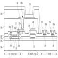
도 2는 본 발명의 일 실시예에 따른 유기전계발광장치의 구조를 보여주는 단면도이다.2 is a cross-sectional view illustrating a structure of an organic light emitting display device according to an embodiment of the present invention.
도 2에 도시된 바와 같이, 본 발명의 일 실시예에 따른 유기전계발광장치는, 기판(200), 반도체층(201), 복수의 절연막(210, 220, 230, 240), 복수의 콘택홀(220a, 220b, 230a, 230b, 230c, 240a), 게이트 전극(211), 소스 전극(221), 드레인 전극(222), 제 1 및 제 2 스토리지 전극(212, 223), 제 1 및 제 2 금속층(231, 232), 애노드 전극(241), 뱅크층(250) 및 유기발광층(251)을 포함한다.As shown in FIG. 2, an organic light emitting display device according to an embodiment of the present invention includes a
기판(200) 상에 소스 영역(201a) 및 드레인 영역(201b)을 포함하는 반도체층(201)이 형성되어 있고, 그 상부에 제 1 절연막(210)이 형성되어 있다. 제 1 절연막(210) 상에는 게이트 전극(211)과 제 1 스토리지 전극(212)이 형성되어 있다. 게이트 전극(211)은 게이트 신호에 의해 주기적으로 인가되는 데이터 신호를 인가 받아 반도체층(201)에 채널을 형성한다.The
게이트 전극(211) 및 제 1 스토리지 전극(212) 상부에는 제 2 절연막(220)이 형성되어 있다. 제 2 절연막(220)이 패터닝되면, 소스 영역(201a) 및 드레인 영역(201b)을 외부로 노출시키는 제 1 콘택홀(220a) 및 제 2 콘택홀(220b)이 형성되는데, 이들 영역에 소스 전극(221) 및 드레인 전극(222)이 각각 형성된다. 따라서 소스 전극(221) 및 드레인 전극(222)은 소스 영역(201a) 및 드레인 영역(201b)에 직접 접촉하게 된다. 이에 따라, 게이트 전극(211)에 신호가 인가되면 반도체층(201)에 채널이 형성되어 소스 전극(221)에서 드레인 전극(222)으로 데이터 신호가 전달된다.The second
또한, 제 1 스토리지 전극(212)과 대응되는 제 2 절연막(220) 상에 제 2 스토리지 전극(223)이 형성되고, 소스 전극(221), 드레인 전극(222) 및 제 2 스토리지 전극(223) 상부에 제 3 절연막(230)이 형성된다. 제 2 스토리지 전극(223)은 제 1 스토리지 전극(212)와 함께 정전용량을 생성한다.In addition, a
그리고, 상기 소스 전극(221), 드레인 전극(222), 제 2 스토리지 전극(223)과 함께 스위칭 트랜지스터(미도시)의 게이트 전극(미도시)과 연결되어 있는 게이트 패드(224) 및 스위칭 트랜지스터의 소스 전극(미도시)과 연결되어 있는 데이터 패드(225)가 각각 형성된다. 상기 스위칭 트랜지스터는 본 발명과 직접적으로 관련이 없는 부분으로, 도면에서의 도시는 생략하기로 한다.The
데이터 패드(225)가 인가받는 데이터 신호는 게이트 패드(224)로부터 전달되는 게이트 신호에 따라 주기적으로 스위칭 트랜지스터의 소스 전극에서 스위칭 트랜지스터의 드레인 전극(미도시)로 전달되고, 스위칭 트랜지스터의 드레인 전극에 연결되어 있는 구동 트랜지스터부의 게이트 전극(211)에 전달된다. 게이트 전극(211)으로 전달된 데이터 신호는 반도체층(201)에 채널을 형성하여 소스 전극(221)의 전원전압을 드레인 전극(222)으로 전달하게 된다. 상기 전원전압은 드레인 전극(222)을 거쳐 유기발광층(251)으로 전달되며, 유기발광층(251)을 구동한다.The data signal to which the
한편, 제 3 절연막(230)을 패터닝하여 드레인 전극(222)을 외부로 노출시키는 제 3 콘택홀(230a)에 제 1 금속층(231)이 형성된다. 또한, 제 3 콘택홀(230a) 형성 시 게이트 패드(224) 및 데이터 패드(225)를 외부로 노출시키는 제 4 콘택홀(230b) 및 제 5 콘택홀(230c)이 동시에 형성될 수 있다.Meanwhile, the
여기서, 제 1 금속층(231)은 몰리브덴(Mo), 구리(Cu), 알루미늄(Al) 중 어느 하나를 포함하는 금속으로 형성될 수 있으며, 특히, 알루미늄 네오디뮴 합금(AlNd) 및 몰리브덴(Mo) 이중층으로 형성되거나, 구리(Cu) 및 몰리브덴 티타늄 합금(MoTi)의 이중층으로 형성될 수 있다. 제 1 금속층(231)의 일단은 드레인 전극(222)과 연결되고, 제 1 금속층(231)의 타단은 애노드 전극(241)과 연결되도록 제 3 절연막(230) 상에서 애노드 전극(241) 쪽으로 연장되어 형성된다. 이렇게, 제 1 금속층(231)이 전원전압을 애노드 전극(241)으로 전달하여 유기발광층(251)을 구동하기 때문에, 제 1 금속층(231)이 픽셀 내에서 배선 역할을 하면서, 전원전압선과 교차되는 메쉬구조를 형성할 수 있다. 이러한, 배선의 메쉬구조를 통해, 전원전압단에서 멀리 떨어진 픽셀에 전달되는 전압을 보상하여, 특히 대면적 유기전계발광표시소자를 구현할 때, 패널의 휘도 균일도를 향상시킬 수 있다.Here, the
또한, 제 2 스토리지 전극(223)과 대응되는 제 3 절연막(230) 상에 제 2 금속층(232)이 형성된다. 제 2 금속층(232) 역시 제 1 금속층(231)과 같이 몰리브덴(Mo), 구리(Cu), 알루미늄(Al) 중 어느 하나를 포함하는 금속으로 형성될 수 있으며, 특히, 알루미늄 네오디뮴 합금(AlNd) 및 몰리브덴(Mo) 이중층으로 형성되거나, 구리(Cu) 및 몰리브덴 티타늄 합금(MoTi)의 이중층으로 형성될 수 있다. 제 2 금속층(232)은 제 2 스토리지 전극(223)과 함께 정전용량을 생성한다. 이렇게 되면, 2 개의 스토리지 전극(222, 223)과 1 개의 금속층(232)을 통해 유기발광층(251)의 구동을 유지할 수 있는 충분한 양의 정전용량을 생성할 수 있다. 따라서, 도 1에서 설명한 바와 같이, 제 1 스토리지 전극(102)을 형성하기 위해 별도로 진행됐던 도핑 공정을 제거하여 공정의 효율성을 향상시킬 수 있다.In addition, a
한편, 제 1 금속층(231) 및 제 2 금속층(232) 상에 제 4 절연막(240)이 형성된다. 제 4 절연막(240)은 평탄화막이며, 폴리아크릴(polyacryl)과 같은 유기물로 형성될 수 있다. 제 4 절연막(240)이 패터닝되어 제 6 콘택홀(240a)이 형성된다. 제 6 콘택홀(240a)에 애노드 전극(241)이 형성되고, 애노드 전극(241)은 제 1 금속층(231)에 직접 접촉된다. 제 1 금속층(231)이 제 3 절연막(230) 및 제 4 절연막(240) 사이에 형성되면서, 제 6 콘택홀(240a)의 단차가 낮아져, 애노드 전극(241)의 전기적 연결의 안정성이 향상된다.The fourth insulating
애노드 전극(241) 및 제 4 절연막(240) 상에 뱅크층(250)이 형성되고, 뱅크층(250) 및 애노드 전극(241) 상에 유기발광층(251)이 형성된다. 유기발광층(251)은 드레인 전극(222)에서 인가된 전원전압을 제 1 금속층(231)을 통해 애노드 전극(241)으로 전달받아 빛을 발광하게 된다.The
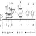
도 3은 본 발명의 다른 실시예에 따른 유기전계발광표시소자를 나타내는 단면도이다.3 is a cross-sectional view illustrating an organic light emitting display device according to another exemplary embodiment of the present invention.
도 3에 도시된 바와 같이, 본 발명의 다른 실시예에 따른 유기전계발광표시장치는 도 2에 도시된 구조와 크게 다르지 않기 때문에, 그 차이점에 대해서만 설명하기로 한다.As shown in FIG. 3, the organic light emitting display device according to another exemplary embodiment of the present invention is not significantly different from the structure shown in FIG. 2, and therefore only the differences will be described.
제 2 절연막(220) 상에 형성된 소스 전극(221), 드레인 전극(222), 제 2 스토리지 전극(223), 게이트 패드(224) 및 데이터 패드(225) 상부에 제 3 절연막(230)이 형성된다.The third
그 다음, 제 3 절연막(230)을 패터닝하여 드레인 전극(222)을 외부로 노출시키는 제 3 콘택홀(230a)을 형성함과 동시에, 게이트 패드(224) 및 데이터 패드(225)를 외부로 노출시키는 제 4 콘택홀(230b) 및 제 5 콘택홀(230c)이 각각 형성된다. 제 4 콘택홀(230b) 및 제 5 콘택홀(230c)에 제 3 금속층(233) 및 제 4 금속층(234)이 각각 형성되어 게이트 패드(224) 및 데이터 패드(225)가 공정 중에 손상되는 것을 방지한다.Next, the third insulating
제 3 금속층(233) 및 제 4 금속층(234)도 제 1 금속층(231) 및 제 2 금속층(232)과 마찬가지로 몰리브덴(Mo), 구리(Cu), 알루미늄(Al) 중 어느 하나를 포함하는 금속으로 형성될 수 있으며, 특히, 알루미늄 네오디뮴 합금(AlNd) 및 몰리브덴(Mo) 이중층으로 형성되거나, 구리(Cu) 및 몰리브덴 티타늄 합금(MoTi)의 이중층으로 형성될 수 있다.Similarly to the
또한, 제 1 금속층(231), 제 2 금속층(232), 제 3 금속층(233) 및 제 4 금속층(234)은 동일한 층인 제 3 절연막(230) 상에 형성되기 때문에, 하나의 공정으로 동시 형성이 가능하다. 상기 여러 기능을 갖는 복수의 금속층(231, 232, 233, 234)을 동시에 형성함으로써, 새로운 구조를 적용하면서도 공정 상의 부담을 줄일 수 있다. 본 발명의 일 실시예에 따른 유기전계발광표시장치의 제조방법에 대해서는 도 4에서 자세히 설명하기로 한다.In addition, since the
이하, 도 4a 내지 도 4d를 참조하여 본 발명의 일 실시예에 따른 유기전계발광표시장치의 제조방법을 보다 구체적으로 설명한다.Hereinafter, a method of manufacturing an organic light emitting display device according to an embodiment of the present invention will be described in more detail with reference to FIGS. 4A to 4D.
도 4a 내지 4d는 본 발명의 일 실시예에 따른 유기전계발광표시장치의 제조방법을 도시한 도면이다.4A to 4D illustrate a method of manufacturing an organic light emitting display device according to an embodiment of the present invention.
먼저, 도 4a에 도시된 바와 같이, 기판(200) 상에 소스 영역(201a) 및 드레인 영역(201b)을 포함하는 반도체층(201)을 형성한다. 소스 영역(201a) 및 드레인 영역(201b)은 P형 또는 N형 불순물을 포함하며, 반도체층(201)은 비정질 실리콘(amorphous silicon), 다결정 실리콘(polysilicon) 또는 산화물(oxide)로 형성할 수 있다.First, as shown in FIG. 4A, a
그 다음, 도 4b에 도시된 바와 같이, 반도체층(201) 상부에 제 1 절연막(210)을 형성하고, 그 상부에 게이트 전극(211) 및 제 1 스토리지 전극(212)를 형성한다. 상기 게이트 전극(211) 및 제 1 스토리지 전극(212)은 스퍼터링(sputtering) 공정을 통해 금속 물질이 제 1 절연막(210) 상부에 증착된 후, 건식 식각(dry etch)으로 필요 없는 부분이 식각되어 형성될 수 있다. 형성 물질로는 몰리브덴(Mo) 등의 금속이 쓰일 수 있다.Next, as shown in FIG. 4B, a first insulating layer 210 is formed on the
그 다음, 도 4c에서 보면, 게이트 전극(211) 및 제 1 스토리지 전극(212) 상부에 제 2 절연막(220)을 형성한 후, 제 2 절연막(220)을 패터닝하여 반도체층(201)의 소스 영역(201a) 및 드레인 영역(201b)를 외부로 노출시키는 제 1 콘택홀(220a) 및 제 2 콘택홀(220b)을 형성한다. 보다 자세히 설명하면, 제 2 절연막(220)에 감광막(photoresist)을 도포한 후 노광 및 현상 공정을 통해 감광막 패턴을 형성하게 된다. 이 감광막 패턴은 제 1 콘택홀(220a) 및 제 2 콘택홀(220b)을 형성하고자 하는 영역을 제외한 제 2 절연막(220) 상부 영역에 감광막이 남아있는 형태로 형성된다. 그 후, 습식 식각(wet etch)을 통해 감광막이 없는 부분의 제 2 절연막(220) 및 제 1 절연막(210)이 식각되어 반도체층(201) 내부의 소스 영역(201a)및 드레인 영역(201b)이 외부로 노출된다.Next, as shown in FIG. 4C, after forming the second
그 다음, 제 1 콘택홀(220a) 및 제 2 콘택홀(220b)에 몰리브덴(Mo) 및 알루미늄 네오디뮴 합금(AlNd) 중 어느 하나를 포함하는 금속을 사용하여 반도체층(201)의 소스 영역(201a) 및 드레인 영역(201b)에 직접 연결되는 소스 전극(221) 및 드레인 전극(222)을 형성한다. 소스 전극(221) 및 드레인 전극(222)은 스퍼터링 공정을 통해 형성되며, 수백 내지 수천 옴스트롱 두께의 단일 또는 복수의 금속막으로 형성될 수 있다. 또한, 제 1 스토리지 전극(212)과 대응되는 제 2 절연막(220) 상에 제 2 스토리지 전극(223)을 형성한다. 제 2 스토리지 전극(223)은 소스 전극(221), 드레인 전극(222)과 동시에 형성될 수 있다.Next, a
그 다음, 도 4d에 도시된 바와 같이, 소스 전극(221), 드레인 전극(222) 및 제 2 스토리지 전극(223) 상부에 제 3 절연막(230)을 형성한다. 제 3 절연막(230)은 플라즈마 화학기상증착 공정을 통해 질화규소(SiNx) 또는 산화규소(SiO2) 등의 절연물질로 형성될 수 있다. 그 후, 제 1 콘택홀(220a) 및 제 2 콘택홀(220b)과 같은 방법으로 드레인 전극(222)을 외부로 노출시키는 제 3 콘택홀(230a)을 형성하여, 이 영역에 제 1 금속층(231)을 형성한다. 제 1 금속층(231)의 일단은 드레인 전극(222)과 연결되고, 제 1 금속층(231)의 타단은 이 후에 형성할 애노드 전극(241)과 연결되도록 제 3 절연막(230) 상에서 소정의 길이를 갖도록 형성된다.Next, as shown in FIG. 4D, a third
또한, 제 2 스토리지 전극(223)과 대응되는 제 3 절연막(230) 상에 제 2 금속층(232)이 형성된다. 제 2 금속층(232)은 제 2 스토리지 전극(223)과 함께 정전용량을 생성하여, 상기 유기발광층(251)의 구동을 유지하는 데 필요한 충분한 양의 정전용량을 생성할 수 있게 된다. 또한, 단순 공정을 통해 제 2 금속층(232)을 형성하여 별도의 도핑 공정을 생략할 수 있어서 공정의 효율성을 향상시킬 수 있다.In addition, a
도 5는 본 발명의 일 실시예에 따른 유기전계발광표시장치의 제조방법을 도시한 도면이다.5 is a diagram illustrating a method of manufacturing an organic light emitting display device according to an embodiment of the present invention.
이하, 도 5a 내지 도 5d를 참조하여 본 발명의 일 실시예에 따른 유기전계발광표시장치의 제조방법을 보다 구체적으로 설명한다.Hereinafter, a method of manufacturing an organic light emitting display device according to an embodiment of the present invention will be described in more detail with reference to FIGS. 5A to 5D.
도 5a 내지 도 5c에 도시된 공정은 상술한 도 4a 내지 도 4c에 도시된 공정과 동일하기 때문에 설명을 생략하도록 한다.Since the process illustrated in FIGS. 5A to 5C is the same as the process illustrated in FIGS. 4A to 4C described above, description thereof will be omitted.
도 5d에 도시된 바와 같이, 소스 전극(221), 드레인 전극(222), 제 2 스토리지 전극(223), 게이트 패드(224) 및 데이터 패드(225) 상에 제 3 절연막(230)을 형성하고, 이를 패터닝하여 제 3 콘택홀(230a), 제 4 콘택홀(230b) 및 제 5 콘택홀(230c)을 형성한다. 제 4 콘택홀(230b) 및 제 5 콘택홀(230c) 또한 제 3 콘택홀(230a)과 동시에 포토리소그라피 공정을 이용하여 제 3 절연막(230)을 식각하여 형성할 수 있다. 그 후, 제 3 콘택홀(230a), 제 2 스토리지 전극(223)과 대응되는 제 3 절연막(230) 상부, 제 4 콘택홀(230b), 및 제 5 콘택홀(230c)에 각각 제 1 금속층(231), 제 2 금속층(232), 제 3 금속층(233) 및 제 4 금속층(234)을 형성한다.As shown in FIG. 5D, the third insulating
또한, 스토리지 전극부의 전극 수를 줄이는 대신 새로운 금속층(231, 232, 233, 234)을 형성하여, 동일 면적 내에서 픽셀 구동부의 설계가 한결 수월해질 수 있으며, 이에 따라 고집적화 및 고해상도 구현이 가능해 진다. 특히, 애노드 전극(241)과 연결되는 제 1 금속층(231)을 전원전압선과 교차하는 메쉬구조로 형성하면, 전원부의 전압이 보상되어 휘도의 균일도를 향상시킬 수 있으며, 따라서 대면적 유기전계발광표시장치 구현 시 고해상도를 구현하면서 동시에 휘도 균일도를 향상시킬 수 있다.In addition, instead of reducing the number of electrodes of the storage electrode unit,
본 발명이 속하는 기술분야의 당업자는 상술한 본 발명이 그 기술적 사상이나 필수적 특징을 변경하지 않고서 다른 구체적인 형태로 실시될 수 있다는 것을 이해할 수 있을 것이다.Those skilled in the art to which the present invention pertains will understand that the above-described present invention can be implemented in other specific forms without changing the technical spirit or essential features.
그러므로, 이상에서 기술한 실시예들은 모든 면에서 예시적인 것이며 한정적인 것이 아닌 것으로 이해해야만 한다. 본 발명의 범위는 상기 상세한 설명보다는 후술하는 특허청구범위에 의하여 나타내어지며, 특허청구범위의 의미 및 범위 그리고 그 등가 개념으로부터 도출되는 모든 변경 또는 변형된 형태가 본 발명의 범위에 포함되는 것으로 해석되어야 한다.It is therefore to be understood that the above-described embodiments are illustrative in all aspects and not restrictive. The scope of the present invention is defined by the appended claims rather than the detailed description and all changes or modifications derived from the meaning and scope of the claims and their equivalents are to be construed as being included within the scope of the present invention do.
200: 기판 201: 반도체층
210: 제 1 절연막 211: 게이트 전극
212: 제 1 스토리지 전극 220: 제 2 절연막
220a: 제 1 콘택홀 220b: 제 2 콘택홀
221: 소스 전극 222: 드레인 전극
223: 제 2 스토리지 전극 224: 게이트 패드
225: 데이터 패드 230: 제 3 절연막
230a: 제 3 콘택홀 230b: 제 4 콘택홀
230c: 제 5 콘택홀 231: 제 1 금속층
232: 제 2 금속층 233: 제 3 금속층
234: 제 4 금속층 240: 제 4 절연막
240a: 제 6 콘택홀 241: 애노드 전극
250: 뱅크층 251: 유기발광층200: substrate 201: semiconductor layer
210: first insulating film 211: gate electrode
212: first storage electrode 220: second insulating film
220a: first contact hole 220b: second contact hole
221: source electrode 222: drain electrode
223: second storage electrode 224: gate pad
225: data pad 230: third insulating film
230a:
230c: fifth contact hole 231: first metal layer
232: second metal layer 233: third metal layer
234: fourth metal layer 240: fourth insulating film
240a: sixth contact hole 241: anode electrode
250: bank layer 251: organic light emitting layer
Claims (10)
Translated fromKorean상기 반도체층 상에 형성된 제 1 절연막;
상기 제 1 절연막의 상부에 형성된 게이트 전극 및 제 1 스토리지 전극;
상기 게이트 전극 및 상기 제 1 스토리지 전극의 상부에 상기 소스 영역 및 상기 드레인 영역을 노출하는 컨택홀을 가지며 형성된 제 2 절연막;
상기 컨택홀을 통해 상기 소스 영역 및 상기 드레인 영역 각각에 연결되는 소스 전극 및 드레인 전극;
상기 제 2 절연막의 상부로 상기 제 1 스토리지 전극과 대응되는 위치에 형성된 제 2 스토리지 전극;
상기 소스 전극, 상기 드레인 전극 및 상기 제 2 스토리지 전극의 상부에 상기 드레인 전극을 노출하는 드레인 컨택홀을 가지며 형성된 제 3 절연막;
일 단이 상기 드레인 컨택홀을 통해 상기 드레인 전극과 접촉하고, 타 단은 상기 드레인 전극의 상부에 형성되는 애노드 전극과 접촉하는 제 1 금속층; 및
상기 제 3 절연막의 상부로 상기 제 2 스토리지 전극과 대응되는 위치에 형성된 제 2 금속층을 포함하는 유기전계발광표시장치.
A semiconductor layer formed on the substrate and including a source region and a drain region;
A first insulating film formed on the semiconductor layer;
A gate electrode and a first storage electrode formed on the first insulating layer;
A second insulating layer formed on the gate electrode and the first storage electrode and having a contact hole exposing the source region and the drain region;
A source electrode and a drain electrode connected to each of the source and drain regions through the contact hole;
A second storage electrode formed at a position corresponding to the first storage electrode on the second insulating layer;
A third insulating layer having a drain contact hole exposing the drain electrode on the source electrode, the drain electrode, and the second storage electrode;
A first metal layer having one end contacting the drain electrode through the drain contact hole and the other end contacting an anode electrode formed on the drain electrode; And
And a second metal layer formed on the third insulating layer to correspond to the second storage electrode.
상기 제 3 절연막은 게이트 패드를 노출하는 제 1 패드 컨택홀과, 데이터 패드를 노출하는 제 2 패드 컨택홀을 더 포함하고,
상기 제 1 패드 컨택홀을 통해 상기 게이트 패드와 연결되는 제 3 금속층과, 상기 제 2 패드 컨택홀을 통해 상기 데이터 패드와 연결되는 제 4 금속층을 더 포함하는 것을 특징으로 하는 유기전계발광표시장치.
The method of claim 1,
The third insulating layer further includes a first pad contact hole exposing the gate pad and a second pad contact hole exposing the data pad,
And a fourth metal layer connected to the gate pad through the first pad contact hole, and a fourth metal layer connected to the data pad through the second pad contact hole.
상기 제 1 금속층, 상기 제 2 금속층, 상기 제 3 금속층 및 상기 제 4 금속층은 동일한 물질로 형성되는 것을 특징으로 하는 유기전계발광표시장치.
3. The method of claim 2,
The first metal layer, the second metal layer, the third metal layer and the fourth metal layer are formed of the same material.
상기 제 1 금속층, 상기 제 2 금속층, 상기 제 3 금속층 및 상기 제 4 금속층은 단일층 또는 복수층으로 형성되는 것을 특징으로 하는 유기전계발광표시장치.
3. The method of claim 2,
And the first metal layer, the second metal layer, the third metal layer and the fourth metal layer are formed in a single layer or a plurality of layers.
상기 제 1 금속층, 상기 제 2 금속층, 상기 제 3 금속층 및 상기 제 4 금속층은 몰리브덴(Mo), 구리(Cu), 알루미늄(Al) 중 어느 하나를 포함하는 금속으로 형성되는 것을 특징으로 하는 유기전계발광표시장치.
3. The method of claim 2,
The first metal layer, the second metal layer, the third metal layer and the fourth metal layer is formed of a metal including any one of molybdenum (Mo), copper (Cu), aluminum (Al). Light emitting display device.
상기 제 1 절연막 상에 게이트 전극 및 제 1 스토리지 전극을 형성하는 단계;
상기 게이트 전극 및 제 1 스토리지 전극의 상부에 상기 반도체층의 상기 소스 영역 및 상기 드레인 영역을 각각 노출시키는 컨택홀을 포함하는 제 2 절연막을 형성하는 단계;
상기 컨택홀을 통해 상기 소스 영역 및 상기 드레인 영역 각각에 연결되는 소스 전극 및 드레인 전극을 형성하는 동시에 상기 제 2 절연막의 상부로 상기 제 1 스토리지 전극과 대응되는 위치에 제 2 스토리지 전극을 형성하는 단계;
상기 소스 전극, 상기 드레인 전극 및 상기 제 2 스토리지 전극의 상부에 상기 드레인 전극을 노출시키는 드레인 컨택홀을 포함하는 제 3 절연막을 형성하는 단계;
상기 드레인 컨택홀을 통해 일 단이 상기 드레인 전극과 접촉하는 제 1 금속층을 형성하는 동시에 상기 제 3 절연막의 상부로 상기 제 2 스토리지 전극과 대응되는 위치에 제 2 금속층을 형성하는 단계 및
상기 제 1 금속층의 상부로 상기 제 1 금속층의 타 단과 접촉하는 애노드 전극을 형성하는 단계를 포함하는 유기전계발광표시장치 제조방법.
Forming a semiconductor layer including a source region and a drain region on the substrate, and forming a first insulating layer on the semiconductor layer;
Forming a gate electrode and a first storage electrode on the first insulating film;
Forming a second insulating layer on the gate electrode and the first storage electrode, the second insulating layer including a contact hole exposing the source region and the drain region of the semiconductor layer, respectively;
Forming a source electrode and a drain electrode connected to each of the source and drain regions through the contact hole, and simultaneously forming a second storage electrode at a position corresponding to the first storage electrode on the second insulating layer; ;
Forming a third insulating layer including a drain contact hole exposing the drain electrode on the source electrode, the drain electrode, and the second storage electrode;
Forming a first metal layer having one end in contact with the drain electrode through the drain contact hole and forming a second metal layer at a position corresponding to the second storage electrode on the third insulating layer;
Forming an anode on the first metal layer, the anode in contact with the other end of the first metal layer.
상기 제 3 절연막을 형성하는 단계는,
게이트 패드를 노출하는 제 1 패드 컨택홀과, 데이터 패드를 노출하는 제 2 패드 컨택홀을 형성하는 단계를 포함하고,
상기 제 1 패드 컨택홀을 통해 상기 게이트 패드와 연결되는 제 3 금속층을 형성하는 단계와,
상기 제 2 패드 콘택홀을 통해 상기 데이터 패드와 연결되는 제 4 금속층을 형성하는 단계를 더 포함하는 것을 특징으로 하는 유기전계발광표시장치 제조방법.
The method according to claim 6,
Forming the third insulating film,
Forming a first pad contact hole exposing the gate pad and a second pad contact hole exposing the data pad,
Forming a third metal layer connected to the gate pad through the first pad contact hole;
And forming a fourth metal layer connected to the data pad through the second pad contact hole.
상기 제 3 금속층을 형성하는 단계 및 상기 제 4 금속층을 형성하는 단계는, 상기 제 1 금속층과 제 2 금속층을 형성하는 단계와 동시에 수행되는 것을 특징으로 하는 유기전계발광표시장치 제조방법.
The method of claim 7, wherein
The forming of the third metal layer and the forming of the fourth metal layer are performed at the same time as the forming of the first metal layer and the second metal layer.
상기 제 1 금속층, 상기 제 2 금속층, 상기 제 3 금속층 및 상기 제 4 금속층을 단일층 또는 복수층으로 형성하는 것을 특징으로 하는 유기전계발광표시장치 제조방법.
The method of claim 7, wherein
And forming the first metal layer, the second metal layer, the third metal layer, and the fourth metal layer in a single layer or in a plurality of layers.
상기 제 1 금속층, 상기 제 2 금속층, 상기 제 3 금속층 및 상기 제 4 금속층을 몰리브덴(Mo), 구리(Cu), 알루미늄(Al) 중 어느 하나를 포함하는 금속으로 형성하는 것을 특징으로 하는 유기전계발광표시장치 제조방법.The method of claim 7, wherein
The first metal layer, the second metal layer, the third metal layer, and the fourth metal layer are formed of a metal including any one of molybdenum (Mo), copper (Cu), and aluminum (Al). Method of manufacturing a light emitting display device.
Priority Applications (2)
| Application Number | Priority Date | Filing Date | Title |
|---|---|---|---|
| KR1020120018612AKR101335527B1 (en) | 2012-02-23 | 2012-02-23 | Organic Light Emitting Diode Display Device and Method for Manufacturing The Same |
| US13/495,907US8680517B2 (en) | 2012-02-23 | 2012-06-13 | Organic light emitting diode display device and method of manufacturing the same |
Applications Claiming Priority (1)
| Application Number | Priority Date | Filing Date | Title |
|---|---|---|---|
| KR1020120018612AKR101335527B1 (en) | 2012-02-23 | 2012-02-23 | Organic Light Emitting Diode Display Device and Method for Manufacturing The Same |
Publications (2)
| Publication Number | Publication Date |
|---|---|
| KR20130096974A KR20130096974A (en) | 2013-09-02 |
| KR101335527B1true KR101335527B1 (en) | 2013-12-02 |
Family
ID=49001877
Family Applications (1)
| Application Number | Title | Priority Date | Filing Date |
|---|---|---|---|
| KR1020120018612AActiveKR101335527B1 (en) | 2012-02-23 | 2012-02-23 | Organic Light Emitting Diode Display Device and Method for Manufacturing The Same |
Country Status (2)
| Country | Link |
|---|---|
| US (1) | US8680517B2 (en) |
| KR (1) | KR101335527B1 (en) |
Families Citing this family (20)
| Publication number | Priority date | Publication date | Assignee | Title |
|---|---|---|---|---|
| KR101888447B1 (en)* | 2012-05-22 | 2018-08-16 | 엘지디스플레이 주식회사 | Method for manufacturing organic light emitting display panel |
| KR102182953B1 (en)* | 2013-11-26 | 2020-11-25 | 엘지디스플레이 주식회사 | Organic light emitting display panel and organic light emitting display device |
| KR102203062B1 (en)* | 2013-11-26 | 2021-01-13 | 엘지디스플레이 주식회사 | Organic Light Emitting Diode Display Device And Method Of Manufacturing The Same |
| US9502653B2 (en)* | 2013-12-25 | 2016-11-22 | Ignis Innovation Inc. | Electrode contacts |
| KR102373082B1 (en)* | 2014-07-16 | 2022-03-10 | 엘지디스플레이 주식회사 | Organic light emitting display device and method of manufacturing the same |
| JP2016062874A (en)* | 2014-09-22 | 2016-04-25 | 株式会社ジャパンディスプレイ | Image display device, manufacturing method thereof, and inspection method of image display device |
| KR102453043B1 (en)* | 2014-12-19 | 2022-10-11 | 엘지디스플레이 주식회사 | Organic light emitting display device and method of manufacturing the same |
| KR102482986B1 (en)* | 2014-12-29 | 2022-12-29 | 엘지디스플레이 주식회사 | Organic light emitting display device and method of manufacturing the same |
| CN104900655A (en)* | 2015-04-14 | 2015-09-09 | 京东方科技集团股份有限公司 | Array substrate and preparation method thereof, and display device |
| KR102540372B1 (en)* | 2015-05-28 | 2023-06-05 | 엘지디스플레이 주식회사 | Organic light emitting display device and method of manufacturing the same |
| KR102515033B1 (en)* | 2015-05-29 | 2023-03-28 | 엘지디스플레이 주식회사 | Organic light emitting display device and method of manufacturing the same |
| KR102451727B1 (en)* | 2015-11-23 | 2022-10-07 | 삼성디스플레이 주식회사 | Organic luminescence emitting display device |
| KR102606279B1 (en)* | 2016-04-04 | 2023-11-27 | 삼성디스플레이 주식회사 | Display apparatus |
| KR102464900B1 (en)* | 2016-05-11 | 2022-11-09 | 삼성디스플레이 주식회사 | Display device |
| KR101859484B1 (en)* | 2016-05-30 | 2018-05-21 | 엘지디스플레이 주식회사 | Display device and method of manufacturing the same |
| KR102726055B1 (en)* | 2016-12-14 | 2024-11-04 | 엘지디스플레이 주식회사 | Organic light emitting display device and method for fabricating the same |
| KR102584517B1 (en)* | 2018-02-28 | 2023-10-05 | 삼성디스플레이 주식회사 | Display Device |
| KR102811558B1 (en)* | 2018-08-17 | 2025-05-22 | 삼성디스플레이 주식회사 | Display device |
| KR102783427B1 (en)* | 2019-01-18 | 2025-03-18 | 삼성디스플레이 주식회사 | Display device |
| KR102761857B1 (en)* | 2019-11-26 | 2025-02-05 | 삼성디스플레이 주식회사 | Organic light emitting display device |
Citations (2)
| Publication number | Priority date | Publication date | Assignee | Title |
|---|---|---|---|---|
| KR20060001402A (en)* | 2004-06-30 | 2006-01-06 | 엘지.필립스 엘시디 주식회사 | Flat panel display device and manufacturing method thereof |
| KR20070109192A (en)* | 2006-05-10 | 2007-11-15 | 삼성전자주식회사 | Display substrate, manufacturing method thereof and display device having same |
Family Cites Families (24)
| Publication number | Priority date | Publication date | Assignee | Title |
|---|---|---|---|---|
| JPH09281508A (en)* | 1996-04-12 | 1997-10-31 | Semiconductor Energy Lab Co Ltd | Liquid crystal display device and its manufacture |
| JP3530362B2 (en)* | 1996-12-19 | 2004-05-24 | 三洋電機株式会社 | Self-luminous image display device |
| US6462722B1 (en)* | 1997-02-17 | 2002-10-08 | Seiko Epson Corporation | Current-driven light-emitting display apparatus and method of producing the same |
| US6204081B1 (en)* | 1999-05-20 | 2001-03-20 | Lg Lcd, Inc. | Method for manufacturing a substrate of a liquid crystal display device |
| TW478014B (en)* | 1999-08-31 | 2002-03-01 | Semiconductor Energy Lab | Semiconductor device and method of manufacturing thereof |
| JP4472073B2 (en)* | 1999-09-03 | 2010-06-02 | 株式会社半導体エネルギー研究所 | Display device and manufacturing method thereof |
| CN1163964C (en)* | 1999-11-05 | 2004-08-25 | 三星电子株式会社 | Thin film transistor array panel for liquid crystal display |
| US6605826B2 (en)* | 2000-08-18 | 2003-08-12 | Semiconductor Energy Laboratory Co., Ltd. | Light-emitting device and display device |
| TW589922B (en)* | 2001-09-19 | 2004-06-01 | Toshiba Corp | Self-emitting display apparatus |
| KR100635042B1 (en)* | 2001-12-14 | 2006-10-17 | 삼성에스디아이 주식회사 | Flat panel display device having front electrode and manufacturing method thereof |
| KR100484591B1 (en)* | 2001-12-29 | 2005-04-20 | 엘지.필립스 엘시디 주식회사 | an active matrix organic electroluminescence display and a manufacturing method of the same |
| KR101035914B1 (en)* | 2004-07-30 | 2011-05-23 | 엘지디스플레이 주식회사 | Flat panel display device and manufacturing method thereof |
| KR101107251B1 (en)* | 2004-12-31 | 2012-01-19 | 엘지디스플레이 주식회사 | Poly thin film transistor substrate and manufacturing method thereof |
| KR101167661B1 (en)* | 2005-07-15 | 2012-07-23 | 삼성전자주식회사 | Wire and method for fabricating interconnection line and thin film transistor substrate and method for fabricating the same |
| JP4882662B2 (en)* | 2006-01-12 | 2012-02-22 | セイコーエプソン株式会社 | Electro-optical device and electronic apparatus |
| KR101276662B1 (en)* | 2006-06-30 | 2013-06-19 | 엘지디스플레이 주식회사 | The organic electro-luminescence device and method for fabricating of the same |
| US7952100B2 (en)* | 2006-09-22 | 2011-05-31 | Semiconductor Energy Laboratory Co., Ltd. | Semiconductor device |
| KR100805124B1 (en)* | 2007-03-05 | 2008-02-21 | 삼성에스디아이 주식회사 | Manufacturing Method of Display Device and Display Device |
| US8421944B2 (en)* | 2007-04-24 | 2013-04-16 | Sharp Kabushiki Kaisha | Display device substrate, display device, and wiring substrate |
| KR101019048B1 (en)* | 2008-11-20 | 2011-03-07 | 엘지디스플레이 주식회사 | Array substrate and its manufacturing method |
| KR101113394B1 (en)* | 2009-12-17 | 2012-02-29 | 삼성모바일디스플레이주식회사 | array substrate of liquid crystal display |
| KR101714539B1 (en)* | 2010-08-24 | 2017-03-23 | 삼성디스플레이 주식회사 | Organic light emitting display device |
| KR101776044B1 (en)* | 2010-11-02 | 2017-09-20 | 엘지디스플레이 주식회사 | Array substrate for organic electro luminescent device and method of fabricating the same |
| KR101876819B1 (en)* | 2011-02-01 | 2018-08-10 | 삼성디스플레이 주식회사 | Thin film transistor array substrate and method of fabricating the same |
- 2012
- 2012-02-23KRKR1020120018612Apatent/KR101335527B1/enactiveActive
- 2012-06-13USUS13/495,907patent/US8680517B2/enactiveActive
Patent Citations (2)
| Publication number | Priority date | Publication date | Assignee | Title |
|---|---|---|---|---|
| KR20060001402A (en)* | 2004-06-30 | 2006-01-06 | 엘지.필립스 엘시디 주식회사 | Flat panel display device and manufacturing method thereof |
| KR20070109192A (en)* | 2006-05-10 | 2007-11-15 | 삼성전자주식회사 | Display substrate, manufacturing method thereof and display device having same |
Also Published As
| Publication number | Publication date |
|---|---|
| US8680517B2 (en) | 2014-03-25 |
| KR20130096974A (en) | 2013-09-02 |
| US20130221381A1 (en) | 2013-08-29 |
Similar Documents
| Publication | Publication Date | Title |
|---|---|---|
| KR101335527B1 (en) | Organic Light Emitting Diode Display Device and Method for Manufacturing The Same | |
| US11557638B2 (en) | Array substrate having light-shielding portion and display panel | |
| KR101277606B1 (en) | Display device and manufacturing method thereof | |
| JP3999205B2 (en) | Active matrix organic light emitting display device and method for manufacturing the same | |
| CN104733499B (en) | Organic light emitting diode display device and manufacturing method thereof | |
| US7948167B2 (en) | Organic light emitting device and manufacturing method thereof | |
| KR101503122B1 (en) | Organic Light Emitting Display Device and Manufacturing Method thereof | |
| KR101622645B1 (en) | Method of Manufacturing of the Organic Light Emitting Display Device | |
| CN106486526A (en) | Organic light emitting diode display | |
| CN1967877B (en) | Thin film transistor and method of fabricating the same | |
| JP2015015241A (en) | Organic light emitting display device and organic light emitting display device manufacturing method | |
| KR20070074594A (en) | Method and display using integrated zinc oxide row and column drivers with organic light emitting diodes | |
| CN112419908B (en) | Display device and semiconductor device | |
| JP2005078073A (en) | Organic electroluminescence display | |
| CN111293125A (en) | Display device and method for manufacturing the same | |
| US7968873B2 (en) | Organic light emitting display and manufacturing method thereof | |
| TW201334040A (en) | Method for manufacturing pixel structure for organic light emitting display | |
| CN104681747B (en) | The method for manufacturing display device | |
| US9231041B2 (en) | Organic light emitting diode display device and method of manufacturing the same | |
| KR20090002717A (en) | Electroluminescent element and manufacturing method thereof | |
| JP2008066323A (en) | Display device and manufacturing method thereof | |
| CN115988916A (en) | Display substrate, manufacturing method thereof, and display device | |
| KR100899428B1 (en) | Organic light emitting display device and manufacturing method thereof | |
| US7129524B2 (en) | Organic electroluminescent device and method for fabricating the same | |
| KR20100123535A (en) | Method of fabricating array substrate |
Legal Events
| Date | Code | Title | Description |
|---|---|---|---|
| PA0109 | Patent application | Patent event code:PA01091R01D Comment text:Patent Application Patent event date:20120223 | |
| A201 | Request for examination | ||
| PA0201 | Request for examination | Patent event code:PA02012R01D Patent event date:20120224 Comment text:Request for Examination of Application Patent event code:PA02011R01I Patent event date:20120223 Comment text:Patent Application | |
| E902 | Notification of reason for refusal | ||
| PE0902 | Notice of grounds for rejection | Comment text:Notification of reason for refusal Patent event date:20130715 Patent event code:PE09021S01D | |
| PG1501 | Laying open of application | ||
| E701 | Decision to grant or registration of patent right | ||
| PE0701 | Decision of registration | Patent event code:PE07011S01D Comment text:Decision to Grant Registration Patent event date:20131120 | |
| GRNT | Written decision to grant | ||
| PR0701 | Registration of establishment | Comment text:Registration of Establishment Patent event date:20131126 Patent event code:PR07011E01D | |
| PR1002 | Payment of registration fee | Payment date:20131126 End annual number:3 Start annual number:1 | |
| PG1601 | Publication of registration | ||
| FPAY | Annual fee payment | Payment date:20161012 Year of fee payment:4 | |
| PR1001 | Payment of annual fee | Payment date:20161012 Start annual number:4 End annual number:4 | |
| FPAY | Annual fee payment | Payment date:20171016 Year of fee payment:5 | |
| PR1001 | Payment of annual fee | Payment date:20171016 Start annual number:5 End annual number:5 | |
| FPAY | Annual fee payment | Payment date:20181015 Year of fee payment:6 | |
| PR1001 | Payment of annual fee | Payment date:20181015 Start annual number:6 End annual number:6 | |
| PR1001 | Payment of annual fee | Payment date:20201019 Start annual number:8 End annual number:8 | |
| PR1001 | Payment of annual fee | Payment date:20211101 Start annual number:9 End annual number:9 | |
| PR1001 | Payment of annual fee | Payment date:20221017 Start annual number:10 End annual number:10 | |
| PR1001 | Payment of annual fee | Payment date:20231016 Start annual number:11 End annual number:11 | |
| PR1001 | Payment of annual fee | Payment date:20241015 Start annual number:12 End annual number:12 |