KR101332517B1 - Apparatus and method for processing authentication information - Google Patents
Apparatus and method for processing authentication informationDownload PDFInfo
- Publication number
- KR101332517B1 KR101332517B1KR1020120091197AKR20120091197AKR101332517B1KR 101332517 B1KR101332517 B1KR 101332517B1KR 1020120091197 AKR1020120091197 AKR 1020120091197AKR 20120091197 AKR20120091197 AKR 20120091197AKR 101332517 B1KR101332517 B1KR 101332517B1
- Authority
- KR
- South Korea
- Prior art keywords
- puf
- password
- unique key
- user
- information processing
- Prior art date
- Legal status (The legal status is an assumption and is not a legal conclusion. Google has not performed a legal analysis and makes no representation as to the accuracy of the status listed.)
- Active
Links
Images


Classifications
- H—ELECTRICITY
- H04—ELECTRIC COMMUNICATION TECHNIQUE
- H04L—TRANSMISSION OF DIGITAL INFORMATION, e.g. TELEGRAPHIC COMMUNICATION
- H04L9/00—Cryptographic mechanisms or cryptographic arrangements for secret or secure communications; Network security protocols
- H04L9/06—Cryptographic mechanisms or cryptographic arrangements for secret or secure communications; Network security protocols the encryption apparatus using shift registers or memories for block-wise or stream coding, e.g. DES systems or RC4; Hash functions; Pseudorandom sequence generators
- H—ELECTRICITY
- H04—ELECTRIC COMMUNICATION TECHNIQUE
- H04L—TRANSMISSION OF DIGITAL INFORMATION, e.g. TELEGRAPHIC COMMUNICATION
- H04L9/00—Cryptographic mechanisms or cryptographic arrangements for secret or secure communications; Network security protocols
- H04L9/32—Cryptographic mechanisms or cryptographic arrangements for secret or secure communications; Network security protocols including means for verifying the identity or authority of a user of the system or for message authentication, e.g. authorization, entity authentication, data integrity or data verification, non-repudiation, key authentication or verification of credentials
- H04L9/3271—Cryptographic mechanisms or cryptographic arrangements for secret or secure communications; Network security protocols including means for verifying the identity or authority of a user of the system or for message authentication, e.g. authorization, entity authentication, data integrity or data verification, non-repudiation, key authentication or verification of credentials using challenge-response
- H04L9/3278—Cryptographic mechanisms or cryptographic arrangements for secret or secure communications; Network security protocols including means for verifying the identity or authority of a user of the system or for message authentication, e.g. authorization, entity authentication, data integrity or data verification, non-repudiation, key authentication or verification of credentials using challenge-response using physically unclonable functions [PUF]
- G—PHYSICS
- G09—EDUCATION; CRYPTOGRAPHY; DISPLAY; ADVERTISING; SEALS
- G09C—CIPHERING OR DECIPHERING APPARATUS FOR CRYPTOGRAPHIC OR OTHER PURPOSES INVOLVING THE NEED FOR SECRECY
- G09C1/00—Apparatus or methods whereby a given sequence of signs, e.g. an intelligible text, is transformed into an unintelligible sequence of signs by transposing the signs or groups of signs or by replacing them by others according to a predetermined system
- H—ELECTRICITY
- H04—ELECTRIC COMMUNICATION TECHNIQUE
- H04L—TRANSMISSION OF DIGITAL INFORMATION, e.g. TELEGRAPHIC COMMUNICATION
- H04L9/00—Cryptographic mechanisms or cryptographic arrangements for secret or secure communications; Network security protocols
- H04L9/06—Cryptographic mechanisms or cryptographic arrangements for secret or secure communications; Network security protocols the encryption apparatus using shift registers or memories for block-wise or stream coding, e.g. DES systems or RC4; Hash functions; Pseudorandom sequence generators
- H04L9/0618—Block ciphers, i.e. encrypting groups of characters of a plain text message using fixed encryption transformation
- H04L9/0631—Substitution permutation network [SPN], i.e. cipher composed of a number of stages or rounds each involving linear and nonlinear transformations, e.g. AES algorithms
- H—ELECTRICITY
- H04—ELECTRIC COMMUNICATION TECHNIQUE
- H04L—TRANSMISSION OF DIGITAL INFORMATION, e.g. TELEGRAPHIC COMMUNICATION
- H04L9/00—Cryptographic mechanisms or cryptographic arrangements for secret or secure communications; Network security protocols
- H04L9/08—Key distribution or management, e.g. generation, sharing or updating, of cryptographic keys or passwords
- H04L9/0861—Generation of secret information including derivation or calculation of cryptographic keys or passwords
- H04L9/0863—Generation of secret information including derivation or calculation of cryptographic keys or passwords involving passwords or one-time passwords
- H—ELECTRICITY
- H04—ELECTRIC COMMUNICATION TECHNIQUE
- H04L—TRANSMISSION OF DIGITAL INFORMATION, e.g. TELEGRAPHIC COMMUNICATION
- H04L9/00—Cryptographic mechanisms or cryptographic arrangements for secret or secure communications; Network security protocols
- H04L9/08—Key distribution or management, e.g. generation, sharing or updating, of cryptographic keys or passwords
- H04L9/0861—Generation of secret information including derivation or calculation of cryptographic keys or passwords
- H04L9/0866—Generation of secret information including derivation or calculation of cryptographic keys or passwords involving user or device identifiers, e.g. serial number, physical or biometrical information, DNA, hand-signature or measurable physical characteristics
- H—ELECTRICITY
- H04—ELECTRIC COMMUNICATION TECHNIQUE
- H04L—TRANSMISSION OF DIGITAL INFORMATION, e.g. TELEGRAPHIC COMMUNICATION
- H04L9/00—Cryptographic mechanisms or cryptographic arrangements for secret or secure communications; Network security protocols
- H04L9/08—Key distribution or management, e.g. generation, sharing or updating, of cryptographic keys or passwords
- H04L9/0861—Generation of secret information including derivation or calculation of cryptographic keys or passwords
- H04L9/0877—Generation of secret information including derivation or calculation of cryptographic keys or passwords using additional device, e.g. trusted platform module [TPM], smartcard, USB or hardware security module [HSM]
- H—ELECTRICITY
- H04—ELECTRIC COMMUNICATION TECHNIQUE
- H04L—TRANSMISSION OF DIGITAL INFORMATION, e.g. TELEGRAPHIC COMMUNICATION
- H04L9/00—Cryptographic mechanisms or cryptographic arrangements for secret or secure communications; Network security protocols
- H04L9/08—Key distribution or management, e.g. generation, sharing or updating, of cryptographic keys or passwords
- H04L9/0894—Escrow, recovery or storing of secret information, e.g. secret key escrow or cryptographic key storage
- H—ELECTRICITY
- H04—ELECTRIC COMMUNICATION TECHNIQUE
- H04L—TRANSMISSION OF DIGITAL INFORMATION, e.g. TELEGRAPHIC COMMUNICATION
- H04L9/00—Cryptographic mechanisms or cryptographic arrangements for secret or secure communications; Network security protocols
- H04L9/14—Cryptographic mechanisms or cryptographic arrangements for secret or secure communications; Network security protocols using a plurality of keys or algorithms
- H—ELECTRICITY
- H04—ELECTRIC COMMUNICATION TECHNIQUE
- H04L—TRANSMISSION OF DIGITAL INFORMATION, e.g. TELEGRAPHIC COMMUNICATION
- H04L9/00—Cryptographic mechanisms or cryptographic arrangements for secret or secure communications; Network security protocols
- H04L9/32—Cryptographic mechanisms or cryptographic arrangements for secret or secure communications; Network security protocols including means for verifying the identity or authority of a user of the system or for message authentication, e.g. authorization, entity authentication, data integrity or data verification, non-repudiation, key authentication or verification of credentials
- H04L9/3226—Cryptographic mechanisms or cryptographic arrangements for secret or secure communications; Network security protocols including means for verifying the identity or authority of a user of the system or for message authentication, e.g. authorization, entity authentication, data integrity or data verification, non-repudiation, key authentication or verification of credentials using a predetermined code, e.g. password, passphrase or PIN
- H04L9/3231—Biological data, e.g. fingerprint, voice or retina
- H—ELECTRICITY
- H04—ELECTRIC COMMUNICATION TECHNIQUE
- H04L—TRANSMISSION OF DIGITAL INFORMATION, e.g. TELEGRAPHIC COMMUNICATION
- H04L2209/00—Additional information or applications relating to cryptographic mechanisms or cryptographic arrangements for secret or secure communication H04L9/00
- H04L2209/12—Details relating to cryptographic hardware or logic circuitry
- H—ELECTRICITY
- H04—ELECTRIC COMMUNICATION TECHNIQUE
- H04L—TRANSMISSION OF DIGITAL INFORMATION, e.g. TELEGRAPHIC COMMUNICATION
- H04L2209/00—Additional information or applications relating to cryptographic mechanisms or cryptographic arrangements for secret or secure communication H04L9/00
- H04L2209/24—Key scheduling, i.e. generating round keys or sub-keys for block encryption
Landscapes
- Engineering & Computer Science (AREA)
- Computer Security & Cryptography (AREA)
- Computer Networks & Wireless Communication (AREA)
- Signal Processing (AREA)
- Theoretical Computer Science (AREA)
- General Physics & Mathematics (AREA)
- Physics & Mathematics (AREA)
- Health & Medical Sciences (AREA)
- Life Sciences & Earth Sciences (AREA)
- Biodiversity & Conservation Biology (AREA)
- Biomedical Technology (AREA)
- General Health & Medical Sciences (AREA)
- Semiconductor Integrated Circuits (AREA)
- Storage Device Security (AREA)
- Design And Manufacture Of Integrated Circuits (AREA)
Abstract
Description
Translated fromKorean디지털 보안 분야에 연관되며, 보다 특정하게는 바이오 정보를 저장하고 처리하는 장치 및 방법에 연관된다. 또한, 바이오 정보 및/또는 사용자 패스워드를 안전하게 저장하고 처리하여, 전자장치의, 임베디드 시스템(Embedded system), SoC(System on Chip), 스마트 카드(Smart Card), 및 USIM(Universal Subscriber Identity Module) 등의 디바이스의 보안/인증에 사용하는 방법에 연관된다.It relates to the field of digital security, and more particularly to apparatus and methods for storing and processing bioinformation. In addition, bio information and / or user passwords are securely stored and processed, such as embedded systems, system on chips (SoCs), smart cards, and universal subscriber identity modules (USIM) of electronic devices. Associated with the method used for security / authentication of the device.
정보화 사회가 고도화 됨에 따라 개인 프라이버시 보호의 필요성도 높아지고 있고, 인증 수단의 안전성이 중요한 기술적 이슈로 제기되고 있다.As the information society becomes more advanced, the necessity of protecting personal privacy is increasing, and the safety of authentication means is being raised as an important technical issue.
특히, 전자금융, 스마트카드(Smart Card), M2M(Machine to machine) 기술 등에는 사용자 또는 기기를 식별하는 인증키의 보안 신뢰성이 높은 수준으로 요구된다. 이하 본 명세서에서는 이러한 인증키(Authentication key)를 식별키(Identification key) 또는 단순히 키(Key)로 지칭하기로 한다.In particular, electronic banking, smart cards, and machine-to-machine (M2M) technologies require a high level of security reliability of authentication keys that identify users or devices. Hereinafter, this authentication key will be referred to as an identification key or simply a key.
인증에는 소유 기반(Possession-based) 인증과, 지식 기반(Knowledge-based) 인증이 가능하다. 전자는 특정한 객체를 소유하고 있는 것에 의해 인증을 수행하는 것이고, 후자는 암호(Password) 등에 의해 인증을 수행하는 것으로 이해할 수 있다.Authentication includes Possession-based authentication and Knowledge-based authentication. The former can be understood as performing authentication by owning a specific object, and the latter can be understood as performing authentication by password or the like.
상기 두 방식은 각각의 장단점을 가지기 때문에, 인증의 안전성을 위해 이러한 소유 기반 인증과 지식 기반 인증을 모두 수행하는 기술들이 소개되고 있다.Since the two methods have advantages and disadvantages, techniques for performing both of the ownership-based and knowledge-based authentication have been introduced for the security of authentication.
한편, PUF (Physically Unclonable Function)는 예측 불가능한 (Unpredictable) 디지털 값을 제공할 수 있다. 개개의 PUF들은 정확한 제조 공정이 주어지고, 동일한 공정에서 제조되더라도, 상기 개개의 PUF들이 제공하는 디지털 값은 다르다.On the other hand, a Physically Unclonable Function (PUF) can provide an unpredictable digital value. Although the individual PUFs are given an exact manufacturing process and are manufactured in the same process, the digital values provided by the individual PUFs are different.
따라서, 복제가 불가능한 POWF (Physical One-Way Function practically impossible to be duplicated)로 지칭될 수도 있다.Thus, it may be referred to as physical one-way function practically impossible to be duplicated (POWF).
이러한 PUF는 보안 및/또는 인증을 위한 암호 키의 생성에 이용될 수 있다. 이를테면, 디바이스를 다른 디바이스와 구별하기 위한 유니크 키(Unique key to distinguish devices from one another)를 제공하기 위해 PUF가 이용될 수 있다.Such a PUF may be used to generate cryptographic keys for security and / or authentication. For example, PUF may be used to provide a unique key to distinguish devices from one another.
그러나, PUF가 생성한 키 자체를 인증에 사용하는 경우, 사용자가 식별키를 기억하기 어려운 경우도 있다. 한편, 사용자 입력 패스워드 및/또는 사용자의 바이오 정보를 인증 키로 사용하는 경우 이를 단말에 저장하였을 때의 안전성이 높은 수준으로 보장되어야 한다.However, when the key itself generated by the PUF is used for authentication, it may be difficult for the user to remember the identification key. On the other hand, when using the user input password and / or the user's bio-information as the authentication key, the safety when storing it in the terminal should be guaranteed to a high level.
일측에 따르면, 반도체 제조 공정 상의 공정 편차를 이용하여 적어도 하나의 유니크 키를 생성하는 PUF; 및 상기 유니크 키를 이용하여 사용자로부터 수신한 패스워드를 암호화하여 식별키를 생성하는 암호화부를 포함하는 정보 처리 장치가 제공된다.According to one side, a PUF for generating at least one unique key using the process deviation in the semiconductor manufacturing process; And an encryption unit for generating an identification key by encrypting the password received from the user using the unique key.
일실시예에 따르면, 상기 PUF는 반도체의 전도성 레이어 사이에 형성되는 인터-레이어 컨택이 상기 전도성 레이어를 단락 하는지의 여부를 이용하여 상기 유니크 키를 생성할 수 있다.According to an embodiment, the PUF may generate the unique key using whether an inter-layer contact formed between the conductive layers of the semiconductor shorts the conductive layer.
이 경우, 상기 반도체의 전도성 레이어 사이에 형성되는 상기 인터-레이어 컨택은, 상기 반도체 제조 공정에서 제공되는 디자인 룰에 따른 사이즈 보다 작도록 구성될 수 있다.In this case, the inter-layer contact formed between the conductive layers of the semiconductor may be configured to be smaller than the size according to the design rule provided in the semiconductor manufacturing process.
일실시예에 따르면, 상기 PUF는, 상기 반도체의 전도성 레이어 사이에 형성되는 상기 인터-레이어 컨택이 상기 전도성 레이어를 단락 하는 확률과 단락 하지 못하는 확률의 차이가 미리 지정된 오차 범위 내에 있도록 하는 상기 인터-레이어 컨택의 사이즈를 가질 수 있다.According to an embodiment, the PUF may be configured such that the difference between the probability that the inter-layer contact formed between the conductive layers of the semiconductor shorts the conductive layer and the probability of not shorting it is within a predetermined error range. It may have a size of a layer contact.
일실시예에 따르면, 상기 PUF는, 한 쌍의 전도성 레이어와 그 사이를 연결하는 하나의 인터-레이어 컨택을 이용하여 1 비트의 디지털 값을 생성하는 단위 구조를 N 개 가져서 - 단, N은 자연수임 -, 상기 N 개의 단위 구조를 통해 N 비트의 유니크 키를 생성할 수 있다.According to one embodiment, the PUF has N unit structures that generate a 1-bit digital value using a pair of conductive layers and a single inter-layer contact therebetween, provided that N is natural. Commitment-A unique key of N bits can be generated through the N unit structures.
이 경우, 상기 PUF는 N 비트의 디지털 값을 생성하고, 상기 정보 처리 장치는 상기 N 비트의 유니크 키에 포함된 디지털 값들을 k 개 단위로 그룹핑 하고 - 단, k는 자연수임 -, 그룹핑된 복수 개의 그룹들 중 제1 그룹 및 제2 그룹을 비교하여, 상기 제1 그룹에 포함된 k개의 디지털 비트로 구성된 값이 상기 제2 그룹에 포함된 k개의 디지털 비트로 구성된 값보다 큰 경우에 상기 제1 그룹과 상기 제2 그룹을 대표하는 디지털 값을 1로 결정할 수 있다.In this case, the PUF generates N-bit digital values, and the information processing apparatus groups the digital values included in the N-bit unique key by k units, where k is a natural number. Comparing the first group and the second group among the groups, and the first group when the value composed of k digital bits included in the first group is greater than the value composed of k digital bits included in the second group. And a digital value representing the second group may be determined as 1.
여기서, 상기 정보 처리 장치는, 상기 제1 그룹에 포함된 k개의 디지털 비트로 구성된 값이 상기 제2 그룹에 포함된 k개의 디지털 비트로 구성된 값이 같은 경우, 설정에 따라 선택적으로, 상기 제1 그룹과 상기 제2 그룹의 대표하는 디지털 값을 1 또는 0 중 어느 한 쪽으로 결정하거나 또는 상기 제1 그룹과 상기 제2 그룹의 대표하는 디지털 값을 결정하지 않을 수 있다.Here, the information processing apparatus, if the value composed of k digital bits included in the first group is the same as the value composed of k digital bits included in the second group, optionally according to a setting, The representative digital value of the second group may be determined to be either 1 or 0, or the representative digital value of the first group and the second group may not be determined.
일실시예에 따르면, 상기 암호화부는, 상기 유니크 키를 라운드 키로 사용하여 상기 패스워드를 N 회 - N은 자연수 - 암호화하여 상기 식별키를 생성할 수 있다.According to an embodiment, the encryption unit may generate the identification key by encrypting the password N times-N is a natural number-using the unique key as a round key.
이 경우, 상기 암호화부는, AES 방법 또는 T-DES 방법으로 상기 패스워드를 암호화하여 상기 식별키를 생성할 수 있다.In this case, the encryption unit may generate the identification key by encrypting the password by the AES method or the T-DES method.
다른 일측에 따르면, 반도체 제조 공정 상의 공정 편차를 이용하여 적어도 하나의 유니크 키를 생성하는 PUF; 및 상기 유니크 키를 이용하여 입력된 바이오 정보를 암호화하여 식별키를 생성하는 암호화부를 포함하는 정보 처리 장치가 제공된다.According to another aspect, a PUF for generating at least one unique key using a process deviation in the semiconductor manufacturing process; And an encryption unit for generating an identification key by encrypting the bio information input using the unique key.
일실시예에 따르면, 상기 PUF는 반도체의 전도성 레이어 사이에 형성되는 인터-레이어 컨택이 상기 전도성 레이어를 단락 하는지의 여부를 이용하여 상기 유니크 키를 생성할 수 있다.According to an embodiment, the PUF may generate the unique key using whether an inter-layer contact formed between the conductive layers of the semiconductor shorts the conductive layer.
일실시예에 따르면, 상기 반도체의 전도성 레이어 사이에 형성되는 상기 인터-레이어 컨택은, 상기 반도체 제조 공정에서 제공되는 디자인 룰에 따른 사이즈 보다 작도록 구성될 수 있다.According to an embodiment, the inter-layer contact formed between the conductive layers of the semiconductor may be configured to be smaller than the size according to the design rule provided in the semiconductor manufacturing process.
한편, 상기 PUF는, 상기 반도체의 전도성 레이어 사이에 형성되는 상기 인터-레이어 컨택이 상기 전도성 레이어를 단락 하는 확률과 단락 하지 못하는 확률의 차이가 미리 지정된 오차 범위 내에 있도록 하는 상기 인터-레이어 컨택의 사이즈를 가질 수 있다.On the other hand, the PUF is the size of the inter-layer contact so that the difference between the probability that the inter-layer contact formed between the conductive layer of the semiconductor shorts the conductive layer and the probability of not shorting it is within a predetermined error range. It can have
또 다른 일측에 따르면, 반도체 제조 공정 상의 공정 편차를 이용하여 적어도 하나의 디지털 값으로 구성된 유니크 키를 생성하는 적어도 하나의 PUF를 포함하고, 상기 적어도 하나의 PUF 중 적어도 하나가 제공하는 적어도 하나의 유니크 키를 이용하여 사용자로부터 수신한 패스워드 또는 바이오 정보 중 적어도 하나를 암호화하여 식별키를 생성하는 암호화부를 포함하는 정보 처리 장치가 제공된다.According to another aspect, at least one PUF for generating a unique key consisting of at least one digital value using a process deviation in the semiconductor manufacturing process, at least one unique provided by at least one of the at least one PUF Provided is an information processing apparatus including an encryption unit for generating an identification key by encrypting at least one of a password or bio information received from a user using a key.
일실시예에 따르면, 상기 암호화부는, 상기 적어도 하나의 유니크 키를 라운드 키로 사용하여 상기 패스워드 또는 상기 바이오 정보 중 적어도 하나를 N 회 - N은 자연수 - 암호화하여 상기 식별키를 생성할 수 있다.According to an embodiment, the encryption unit may generate the identification key by encrypting at least one of the password or the bio information N times-N is a natural number-using the at least one unique key as a round key.
일실시예에 따르면, 상기 암호화부는, AES 방법 또는 T-DES 방법으로 상기 패스워드 또는 상기 바이오 정보 중 적어도 하나를 암호화하여 상기 식별키를 생성할 수 있다.According to an embodiment, the encryption unit may generate the identification key by encrypting at least one of the password or the bio information by an AES method or a T-DES method.
일실시예에 따르면, 상기 적어도 하나의 PUF 각각은 반도체의 전도성 레이어 사이에 형성되는 인터-레이어 컨택이 상기 전도성 레이어 사이를 단락 하는지의 여부를 이용하여 상기 유니크 키를 생성할 수 있다.According to one embodiment, each of the at least one PUF may generate the unique key using whether or not an inter-layer contact formed between the conductive layers of the semiconductor shorts between the conductive layers.
이 경우, 상기 인터-레이어 컨택은, 상기 반도체 제조 공정에서 제공되는 디자인 룰에 따른 사이즈 보다 작도록 구성될 수 있다.In this case, the inter-layer contact may be configured to be smaller than the size according to the design rule provided in the semiconductor manufacturing process.
여기서, 상기 PUF는, 상기 반도체의 전도성 레이어 사이에 형성되는 상기 인터-레이어 컨택이 상기 전도성 레이어를 단락 하는 확률과 단락 하지 못하는 확률의 차이가 미리 지정된 오차 범위 내에 있도록 하는, 상기 인터-레이어 컨택의 사이즈를 가질 수 있다.Here, the PUF is such that the difference between the probability that the inter-layer contact formed between the conductive layers of the semiconductor shorts the conductive layer and the probability of not shorting it is within a predetermined error range. It may have a size.
일실시예에 따르면, 상기 정보 처리 장치는, 상기 적어도 하나의 PUF 중 상기 암호화부가 상기 암호화에 이용할 PUF를 선택하는 PUF 선택부를 더 포함할 수 있다.According to an embodiment, the information processing apparatus may further include a PUF selector configured to select a PUF to be used for the encryption unit from the encryption unit among the at least one PUF.
또 다른 일측에 따르면, 정보 처리 장치에 포함된 PUF가, 반도체 제조 공정 상의 공정 편차를 이용하여 적어도 하나의 유니크 키를 생성하는 단계; 및 상기 정보 처리 장치의 암호화부가, 상기 유니크 키를 이용하여, 상기 정보 처리 장치에 입력된 제1 사용자 입력 패스워드 또는 제1 사용자 바이오 정보 중 적어도 하나를 암호화하여 암호화된 패스워드 또는 암호화된 바이오 정보 중 적어도 하나를 생성하는 단계를 포함하는 정보 처리 방법이 제공된다.According to another aspect, the PUF included in the information processing apparatus, generating at least one unique key using the process deviation on the semiconductor manufacturing process; And at least one of a password or encrypted bio information that is encrypted by encrypting at least one of a first user input password or first user bio information input to the information processing device using the unique key. An information processing method is provided that includes generating one.
일실시예에 따르면, 상기 정보 처리 방법은, 사용자로부터 상기 정보 처리 장치에 제2 사용자 입력 패스워드 또는 제2 사용자 바이오 정보 중 적어도 하나가 입력되는 경우, 상기 제2 사용자 입력 패스워드 또는 상기 제2 사용자 바이오 정보 중 적어도 하나를 암호화하는 단계; 및 상기 정보 처리 장치의 인증부가, 암호화된 상기 제2 사용자 입력 패스워드 또는 암호화된 상기 제2 사용자 바이오 정보 중 적어도 하나를 상기 암호화된 패스워드 또는 상기 암호화된 바이오 정보 중 적어도 하나와 비교하여 인증을 수행하는 단계를 더 포함할 수 있다.According to one embodiment, the information processing method, when at least one of a second user input password or second user bio information is input from the user to the information processing device, the second user input password or the second user bio Encrypting at least one of the information; And the authentication unit of the information processing apparatus compares at least one of the encrypted second user input password or the encrypted second user bio information with at least one of the encrypted password or the encrypted bio information to perform authentication. It may further comprise a step.
다른 일실시예에 따르면, 상기 정보 처리 방법은, 사용자로부터 상기 정보 처리 장치에 제2 사용자 입력 패스워드 또는 제2 사용자 바이오 정보 중 적어도 하나가 입력되는 경우, 상기 정보 처리 장치의 암호화부가 상기 암호화된 패스워드 또는 상기 암호화된 바이오 정보 중 적어도 하나를 복호화하여 상기 제1 사용자 입력 패스워드 또는 상기 제1 사용자 바이오 정보 중 적어도 하나를 생성하는 단계; 및 상기 정보 처리 장치의 인증부가, 상기 복호화된 상기 제1 사용자 패스워드 또는 상기 제1 사용자 바이오 정보 중 적어도 하나를, 상기 제2 사용자 입력 패스워드 또는 상기 제2 사용자 바이오 정보 중 적어도 하나와 비교하여 인증을 수행하는 단계를 더 포함할 수 있다.According to another embodiment, in the information processing method, when at least one of a second user input password or second user bio information is input from the user to the information processing apparatus, the encryption unit of the information processing apparatus is the encrypted password. Or generating at least one of the first user input password or the first user bio information by decrypting at least one of the encrypted bio information; And the authentication unit of the information processing apparatus compares at least one of the decrypted first user password or the first user bio information with at least one of the second user input password or the second user bio information to perform authentication. The method may further include performing the step.
도 1은 일실시예에 따른 정보 처리 장치를 도시한다.
도 2는 일실시예에 따른 PUF의 구성을 설명하기 위한 개념도이다.
도 3은 도 2의 실시예에 따른 PUF를 설명하기 위한 그래프이다.
도 4는 다른 일실시예에 따른 PUF 의 구성을 설명하기 위한 개념도이다.
도 5는 일실시예에 따른 PUF에서 유니크 키를 생성할 수 있도록 하는 인터-레이어 컨택 어레이를 도시한다.
도 6은 일실시예에 따라 PUF가 생성한 유니크 키를 인식하는 과정을 설명하기 위한 도면이다.
도 7은 일실시예에 따라 PUF가 생성한 유니크 키의 밸런싱 과정을 설명하기 위한 개념도이다.
도 8은 다른 일실시예에 따른 정보 처리 장치를 도시한다.
도 9는 일실시예에 따라 PUF들이 암호화부 내에 배치되는 예시적 구성을 도시한다.
도 10은 일실시예에 따른 정보 처리 방법에 따라 패스워드 및/또는 바이오 정보를 암호화 하여 저장하는 과정을 도시하는 흐름도이다.
도 11은 도 8의 실시예에 따른 정보 처리 장치가 패스워드 및/또는 바이오 정보를 암호화 하여 저장하는 과정을 도시하는 흐름도이다.
도 12는 일실시예에 따른 정보 처리 장치에서 사용자 입력 패스워드 및/또는 바이오 정보를 인증하는 과정을 도시하는 흐름도이다.
도 13은 다른 일실시예에 따른 정보 처리 장치에서 사용자 입력 패스워드 및/또는 바이오 정보를 인증하는 과정을 도시하는 흐름도이다.1 illustrates an information processing apparatus according to an embodiment.
2 is a conceptual diagram illustrating a configuration of a PUF according to an embodiment.
FIG. 3 is a graph for explaining a PUF according to the embodiment of FIG. 2.
4 is a conceptual diagram illustrating a configuration of a PUF according to another embodiment.
5 illustrates an inter-layer contact array that enables generation of a unique key in a PUF, according to one embodiment.
6 is a diagram for describing a process of recognizing a unique key generated by a PUF, according to an exemplary embodiment.
7 is a conceptual diagram illustrating a balancing process of a unique key generated by a PUF according to an embodiment.
8 illustrates an information processing apparatus according to another embodiment.
9 illustrates an example configuration in which PUFs are disposed in an encryption unit according to an embodiment.
10 is a flowchart illustrating a process of encrypting and storing a password and / or bio information according to an information processing method according to an embodiment.
FIG. 11 is a flowchart illustrating a process of encrypting and storing a password and / or bio information by an information processing apparatus according to the embodiment of FIG. 8.
12 is a flowchart illustrating a process of authenticating a user input password and / or bio information in an information processing apparatus according to an embodiment.
13 is a flowchart illustrating a process of authenticating a user input password and / or bio information in an information processing apparatus according to another embodiment.
이하에서, 본 발명의 일부 실시예를, 첨부된 도면을 참조하여 상세하게 설명한다. 그러나, 본 발명이 실시예들에 의해 제한되거나 한정되는 것은 아니다. 각 도면에 제시된 동일한 참조 부호는 동일한 부재를 나타낸다.Hereinafter, some embodiments of the present invention will be described in detail with reference to the accompanying drawings. However, the present invention is not limited to or limited by the embodiments. Like reference symbols in the drawings denote like elements.
도 1은 일실시예에 따른 정보 처리 장치(100)를 도시한다.1 illustrates an
일실시예에 따른 정보 처리 장치(100)는 사용자로부터 수신되는 패스워드(Password) 및/또는 바이오 정보를 암호화 하여 안전하게 저장하고, 또한 보안 인증을 수행할 수 있다.The
일실시예에 따르면, 정보 처리 장치(100)의 수신부(110)는 사용자가 입력하는 패스워드를 수신할 수 있다.According to an embodiment, the receiving
사용자가 입력한 패스워드를 등록하여, 등록된 패스워드를 이용하여 사용자 및/또는 기기를 인증하는 것이 지식 기반 인증에 대응할 수 있다. 그러나, 사용자 입력 패스워드가 보안 공격에 의해 유출되는 경우, 이러한 지식 기반 인증은 신뢰 할 수 없는 것이 된다.Registering a password entered by the user and authenticating the user and / or the device using the registered password may correspond to knowledge-based authentication. However, if the user input password is leaked by a security attack, such knowledge base authentication becomes unreliable.
따라서, 사용자가 입력한 패스워드를 높은 수준의 보안 처리에 의해 등록하여 관리하는 것이 요구된다.Therefore, it is required to register and manage the password input by the user by a high level of security processing.
일실시예에 따르면, 정보 처리 장치(100)는 수신부(110)에서 수신한 사용자 입력 패스워드를 암호화하여 저장(등록)한다. 상기 수신하는 패스워드는 평문(Plain text)일 수 있다.According to an embodiment, the
일실시예에 따르면, 정보 처리 장치(100)는 반도체 공정 상의 공정 편차를 이용하여 시간에 따라 변하지 않는 무작위의 디지털 값(Digital value)인 유니크 키를 생성하는 PUF(120)를 포함한다.According to an embodiment, the
상기 PUF(120)가 생성한 디지털 값은 이를 테면, N 비트(단, N은 자연수)일 수 있다.The digital value generated by the
PUF(120)가 생성한 유니크 키 자체를 소유 기반의 인증을 위한 식별키로 사용할 수도 있으나, 일실시예에 따르면 상기 유니크 키를 이용하여 상기 사용자 입력 패스워드를 암호화함으로써, 소유 기반 인증과 지식 기반 인증을 모두 제공할 수 있다.The unique key generated by the
이 경우, PUF(120)가 생성한 유니크 키는 외부로 유출되지 않음으로써 높은 수준의 신뢰성과 안전성이 보장될 수 있다. PUF(120)의 구현에 관해서는 보다 상세히 후술한다.In this case, the unique key generated by the
일실시예에 따르면, PUF(120)가 생성한 유니크 키를 AES (Advanced Encryption Standard) 등에서 사용되는 라운드 키(round key)로 이용하여, 사용자로부터 수신된 패스워드를 k 회(단, k는 자연수) 암호화 하여 암호화된 값을 인증을 위한 식별키로 사용할 수 있다.According to an embodiment, using the unique key generated by the
일실시예에 따르면, 암호화부(130)는 상기한 바와 같이, PUF(120)가 생성한 유니크 키를 시드(seed)로 이용하여, 수신부(110)가 수신한 패스워드를 AES 방식 또는 T-DES (Triple Data Encryption Standard) 방식 등으로 k회 암호화하여 인증에 사용될 식별키를 생성한다.According to an embodiment, as described above, the
다만, 상기 AES 방식 또는 T-DES 방식 등은 일부 실시예에 불과하며, DES(Data Encryption Standard) 등 다른 여러 가지 실시예 또한 가능하다.However, the AES method or the T-DES method is just some embodiments, and other various embodiments such as a data encryption standard (DES) are also possible.
일실시예에 따르면, 생성된 식별키는 저장부(140)에 저장될 수 있다.According to an embodiment, the generated identification key may be stored in the
저장부(140)는 OTP(One Time Programmable) 메모리, 플래시(Flash) 메모리 등 다양한 형태의 비휘발성(non-volatile) 메모리 일 수 있다.The
저장부(140)에 저장된 식별키는, 온라인 상에서 사용자 및/또는 기기의 인증을 수행하는 데에 이용될 수 있으며, 상기 패스워드가 유출되더라도 PUF(120)의 복제 불가능성에 의해 동일한 식별키의 생성이 방지된다.The identification key stored in the
또한, 다른 실시예에서는 상기 저장된 식별키는 스마트 카드 등 보안 인증이 필요한 기기 또는 칩(Chip)에 대한 외부의 접근(Access)을 차단하는 게이팅(gating) 역할을 수행할 수도 있다.In another embodiment, the stored identification key may serve as a gating to block external access to a device or chip requiring security authentication, such as a smart card.
따라서, 생성되어 저장된 상기 식별키를 인증/보안의 목적으로 사용하는 용도에 있어서는 일부 실시예에 국한되지 않는다.Thus, the use of the generated and stored identification key for authentication / security purposes is not limited to some embodiments.
한편, 다른 일실시예에 따르면, 정보 처리 장치(100)는 사용자 입력 패스워드뿐만 아니라 사용자의 바이오 정보, 이를테면 지문, 홍채에 연관된 정보를 안전하게 암호화 하여 저장하는 데에 이용될 수도 있다.Meanwhile, according to another exemplary embodiment, the
이 실시예에서, 수신부(110)에 바이오 정보가 수신되면, PUF(120)가 생성한 유니크 키를 이용하여, 암호화부(130)는 상기 바이오 정보를 AES 방식 또는 T-DES (Triple Data Encryption Standard) 방식 등으로 k회 암호화할 수 있다.In this embodiment, when the bio information is received at the
이렇게 암호화하여 생성된 식별키가 저장부(140)에 저장되는 경우, PUF(120)에 의해 생성된 유니크 키 없이는 상기 식별키를 상기 바이오 정보로 복호화 할 수 없으므로 높은 수준의 신뢰성 및 안전성이 제공된다.When the encryption key generated in this way is stored in the
상기한 과정은 사용자 입력 및/또는 바이오 정보를 인증에 사용되는 식별키로서 등록하는 과정으로 이해될 수 있다. 일실시예에 따르면, 정보 처리 장치(100)는 이렇게 등록된 식별키를 이용하여, 사용자 및/또는 기기를 인증하는 인증부(150)를 더 포함할 수 있다.The above process may be understood as a process of registering user input and / or bio information as an identification key used for authentication. According to an embodiment, the
사용자 패스워드를 등록하여 인증에 이용하는 실시예에에서, 인증부(150)는 인증 수행을 위해 입력되는 사용자 패스워드가 등록된 패스워드와 일치하는 지의 여부를 인증할 수 있다.In an embodiment in which a user password is registered and used for authentication, the
일실시예에 따르면, 사용자가 인증 수행을 위해 입력하는 패스워드가 수신부(110)에 입력되면, 암호화부(130)는 PUF(120)가 생성한 유니크 키를 이용하여 상기 입력된 패스워드를 암호화하여 암호화된 패스워드를 인증부(150)에 전달할 수 있다. 그러면, 인증부(150)는 상기 암호화된 패스워드가 저장부(140)에 미리 저장되어 있는 등록된 식별키와 일치하는 지의 여부를 판단하여 패스워드의 인증 성공 또는 인증 실패를 결정할 수 있다.According to an embodiment, when a password inputted by a user to perform authentication is input to the
다른 일실시예에 따르면, 사용자가 인증 수행을 위해 입력하는 패스워드가 수신부(110)에 입력되면, 수신부(110)가 입력된 패스워드를 인증부(150)에 전달한다. 그리고 암호화부(130)는 PUF(120)가 생성한 유니크 키를 이용하여 저장부(140)에 미리 저장되어 있는 식별키를 복호화 하여 복호화된 식별키를 인증부(150)에 전달할 수 있다. 그러면, 인증부(150)는 상기 수신부(110)로부터 전달된 사용자 입력 패스워드와 상기 암호화부(130)로부터 전달된 복호화된 식별키가 일치하는 지의 여부를 판단하여 패스워드의 인증 성공 또는 인증 실패를 결정할 수 있다.According to another embodiment, when a password input by the user to perform authentication is input to the
한편, 바이오 정보를 등록하여 인증에 이용하는 실시예에서, 인증부(150)는 인증 수행을 위해 입력되는 바이오 정보가 등록된 바이오 정보와 일치하는 지의 여부를 인증할 수 있다.Meanwhile, in an embodiment of registering and using bioinformation, the
일실시예에 따르면, 인증 수행을 위한 바이오 정보가 수신부(110)에 입력되면, 암호화부(130)는 PUF(120)가 생성한 유니크 키를 이용하여 상기 입력된 바이오 정보를 암호화하여 암호화된 바이오 정보를 인증부(150)에 전달할 수 있다. 그러면, 인증부(150)는 상기 암호화된 바이오 정보가 저장부(140)에 미리 저장되어 있는 등록된 식별키와 일치하는 지의 여부를 판단하여 패스워드의 인증 성공 또는 인증 실패를 결정할 수 있다.According to an embodiment, when bio information for performing authentication is input to the
다른 일실시예에 따르면, 인증 수행을 위한 바이오 정보가 수신부(110)에 입력되면, 수신부(110)가 입력된 바이오 정보를 인증부(150)에 전달한다. 그리고 암호화부(130)는 PUF(120)가 생성한 유니크 키를 이용하여 저장부(140)에 미리 저장되어 있는 식별키를 복호화 하여 복호화된 식별키를 인증부(150)에 전달할 수 있다. 그러면, 인증부(150)는 상기 수신부(110)로부터 전달된 바이오 정보와 상기 암호화부(130)로부터 전달된 복호화된 식별키가 일치하는 지의 여부를 판단하여 패스워드의 인증 성공 또는 인증 실패를 결정할 수 있다.According to another embodiment, when bio information for performing authentication is input to the
이 실시예는 바이오 정보의 처리에 유용할 수 있다. 바이오 정보, 이를테면 지문이나 홍채 무늬는 입력 시 마다 식별 오차가 있을 수 있어서, 등록 시에 사용된 동일한 오브젝트의 바이오 정보를 추후에 인증 수행 시 다시 입력하더라도, 식별되는 바이오 정보는 완전히 일치하지 않을 수도 있다. 따라서, 통상적인 바이오 정보의 인증 과정도 입력된 바이오 정보와 미리 등록된 바이오 정보의 일치도를 판단하고 있다.This embodiment may be useful for processing bioinformation. Bioinformation, such as fingerprints or iris patterns, may have an identification error for each input, so even if bioinformation of the same object used at the time of registration is re-entered later during authentication, the identified bioinformation may not be completely identical. . Therefore, the normal bio information authentication process also determines the degree of correspondence between the input bio information and the previously registered bio information.
이 실시예에서도, 인증을 위해 입력되어 수신부(110)에 전달된 바이오 정보를 암호화 하지 않고, 인증부(150)에 전달하고, 인증부는 복호화된 식별키와 상기 전달된 바이오 정보를 비교하여 일치도에 따라 인증 성공 또는 인증 실패를 결정할 수 있다.Even in this embodiment, the bio information input for authentication and transmitted to the receiving
이하에서는 일실시예에 따른 PUF(120)의 예시적 구성에 대해 설명한다.Hereinafter, an exemplary configuration of the
일실시예에 따른 PUF(120)는 반도체 제조 공정 상 반도체 소자 상에 생성되는 노드(node) 간의 단락(short) 여부가 확률적으로 결정될 수 있는 구성에 의해 구현된다.According to an embodiment, the
이를테면, PUF(120)는 동일한 반도체 제조 공정에서 발생하는 공정편차(Process-variation)를 이용하여, 전도성 레이어들(conductive layers) 사이의 인터-레이어 컨택이 상기 전도성 레이어들 사이를 단락시키는지의 여부에 따라 N 비트의 디지털 값을 생성한다. 상기 인터-레이어 컨택은, 이를테면 비아(Via)일 수 있으며, 이하에서는 별다른 언급이 없더라도 인터-레이어 컨택은 반도체의 전도성 레이어들 사이를 전기적으로 단락할 수 있는 다양한 전도성 요소를 포함하는 것으로 이해되어야 한다.For example,
인터-레이어 컨택, 이를테면 비아는 전도성 레이어들 사이를 연결하도록 설계되는 것이어서, 통상적으로 인터-레이어 컨택 또는 비아 사이즈는 전도성 레이어들 사이를 단락시키도록 결정된다. 그리고 통상적인 디자인 룰(rule)에서는 전도성 레이어들 사이를 단락시키는 것이 보장되도록 최소한의 비아 사이즈가 정해져 있다.Inter-layer contacts, such as vias, are designed to connect between conductive layers, so that the inter-layer contact or via size is typically determined to short between the conductive layers. And in conventional design rules, a minimum via size is specified to ensure shorting between conductive layers.
그러나, 본 실시예에 따른 PUF(120)의 구현에 있어서는, 인터-레이어 컨택, 이를테면 비아의 사이즈를 디자인 룰에서 정해진 것보다 의도적으로 작게 하여, N 개의 비아 중 일부의 비아는 전도성 레이어들 사이를 단락시키고, 다른 일부의 비아는 상기 전도성 레이어들 사이를 단락시키지 못하게 됨으로써, 각 노드의 단락 여부가 확률적으로 결정된다.However, in the implementation of the
기존의 반도체 공정에서는 인터-레이어 컨택이 전도성 레이어들 사이를 단락시키지 못하면 공정 상 실패한 것이 되나, 실시예들에서는 이를 무작위의 디지털 값인 유니크 키 생성에 이용하는 것이다.In the conventional semiconductor process, if the inter-layer contact fails to short between the conductive layers, the process fails. However, in the embodiments, the inter-layer contact is used to generate a unique key, which is a random digital value.
상기 실시예에 따른 인터-레이어 컨택, 이를테면 비아의 사이즈 설정은 도 2 내지 도 3을 참조하여 보다 상세히 후술한다.Size setting of the inter-layer contact, for example, via according to the embodiment, will be described in more detail later with reference to FIGS. 2 to 3.
한편, PUF(120)의 구현에 대한 다른 일실시예에 따르면, PUF(120)는 반도체 제조 공정 상에서 전도성 라인들 간의 간격 (spacing)을 디자인 룰보다 의도적으로 작게 결정하여, 전도성 라인들 사이의 단락 여부가 확률적으로 결정되도록 하여, 유니크 키가 생성된다.Meanwhile, according to another exemplary embodiment of the implementation of the
이러한 실시예 또한, 종래의 반도체 제조 공정에서, 전도성 라인들 사이의 오픈을 보장하는 디자인 룰인 전도성 레이어 사이의 최소 간격 이하의 간격을 만듦으로써, PUF(120)에 의한 유니크 키가 생성되는 것이다.This embodiment is also to generate a unique key by the
상기 실시예에 따른 전도성 레이어 간격 설정은 도 4를 참조하여 보다 상세히 후술한다.The conductive layer spacing according to the embodiment will be described later in more detail with reference to FIG. 4.
한편, PUF(120)가 생성한 유니크 키는, 상기 전도성 레이어들 사이를 상기 인터-레이어 컨택이 단락하고 있는지를 리드 트랜지스터(read transistor)를 이용하여 식별함으로써 얻어질 수 있다. 리드 트랜지스터의 예시적 구현은 도 6을 참조하여 보다 상세히 후술한다.The unique key generated by the
한편, 상기한 인터-레이어 컨택의 사이즈 조정을 이용하는 실시예에서, 전도성 레이어들 사이를 단락하는 인터-레이어 컨택과 그렇지 못한 인터-레이어 컨택의 비율이 가급적 1/2로 동일한 확률을 가지도록 인터-레이어 컨택의 사이즈를 조정하더라도, 단락이 되는 경우(이를 테면 디지털 값 0)와 그렇지 않은 경우(이를 테면 디지털 값 1)의 비율이 확률적으로 완전히 동일한 것이 보장되지 않을 수도 있다.On the other hand, in the embodiment using the size adjustment of the inter-layer contact described above, the ratio of inter-layer contacts shorting between the conductive layers and non-inter-layer contacts that do not have the same probability is as half as possible. Resizing the layer contacts may not guarantee that the proportions of shorts (such as digital value 0) and otherwise (such as digital value 1) are stochasticly identical.
즉, 인터-레이어 컨택, 이를테면 비아의 사이즈가 디자인 룰에서 정해진 값에 가깝게 커질수록 전도성 레이어들 사이가 단락되는 확률이 커지고, 반대로 작아질수록 단락이 되지 않는 확률이 커진다. 그런데, 단락되는 경우와 단락되지 않는 경우의 확률 중 어느 한 쪽이 커지게 되면, 생성된 유니크 키의 난수성이 저하된다.In other words, as the size of the inter-layer contact, such as a via, increases closer to the value defined in the design rule, the probability of shorting between the conductive layers increases, and conversely, the probability of shorting does not increase. However, when either of the cases of shorting and non-shorting becomes large, the randomness of the generated unique key is lowered.
이러한 문제는 상기한 전도성 라인 사이의 간격(spacing)을 조정하는 실시예에서도 마찬가지이다.This problem also applies to the embodiment of adjusting the spacing between the conductive lines described above.
따라서 일실시예에 따르면, PUF(120)가 생성한 로우 디지털 값(Raw digital values)을 그룹핑하여 각 그룹 사이의 디지털 값을 비교함으로써 PUF(120)가 생성하는 유니크 키를 결정할 수 있다. 이러한 내용은 생성된 디지털 값에 대해 디지털 값 '0'과 디지털 값 '1' 사이의 밸런싱(balancing)을 수행하는 과정으로 이해될 수 있다.Therefore, according to an embodiment, a unique key generated by the
이러한 밸런싱 과정은 도 7을 참조하여 보다 상세히 후술한다.This balancing process will be described later in more detail with reference to FIG. 7.
도 2는 일실시예에 따른 PUF(120) 의 구성을 설명하기 위한 개념도이다.2 is a conceptual diagram illustrating a configuration of the
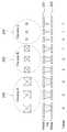
반도체 제조 공정에서 메탈 1 레이어(202)과 메탈 2 레이어(201) 사이에 인터-레이어 컨택의 일 예인 비아들이 형성된 모습의 도시되었다.In the semiconductor fabrication process, vias, which are examples of inter-layer contacts, are formed between the
비아 사이즈를 디자인 룰에 따라 충분히 크게 한 그룹(210)에서는 모든 비아가 메탈 1 레이어(202)와 메탈 2 레이어(201)를 단락시키고 있으며, 이 때 단락 여부를 디지털 값으로 표현하면 모두 0이 된다.In the
한편, 비아 사이즈를 너무 작게 한 그룹(230)에서는 모든 비아가 메탈 1 레이어(202)와 메탈 2 레이어(201)을 단락시키지 못하고 있다. 따라서 이 때 단락 여부를 디지털 값으로 표현하면 모두 1이 된다.On the other hand, in the
그리고, 비아 사이즈를 그룹(210)에서의 사이즈와 그룹(230)에서의 사이즈 사이로 선택한 그룹(220)에서는, 일부의 비아는 메탈 1 레이어(202)와 메탈 2 레이어(201)을 단락시키고, 다른 일부의 비아는 메탈 1 레이어(202)와 메탈 2 레이어(201)을 단락시키지 못하고 있다.And, in
일실시예에 따른 PUF(120)는, 그룹(220)과 같이, 일부의 비아는 메탈 1 레이어(202)와 메탈 2 레이어(201)를 단락시키고, 다른 일부의 비아는 메탈 1 레이어(202)와 메탈 2 레이어(201)를 단락시키지 못하도록 비아 사이즈를 설정하여 구성된다.
비아 사이즈에 대한 디자인 룰은 반도체 제조 공정에 따라 상이할 수 있다. 이를테면 0.18 미크론(um)의 CMOS(Complementary metal-oxide-semiconductor) 공정에서 비아의 디자인 룰이 0.25 미크론으로 설정된다고 하면, 상기 실시예에 따른 PUF(120)에서는 비아 사이즈를 0.19 미크론으로 설정하여, 메탈 레이어들 사이의 단락 여부가 확률적으로 분포하도록 한다.The design rule for the via size may differ depending on the semiconductor manufacturing process. For example, if the design rule of the via is set to 0.25 micron in a Complementary metal-oxide-semiconductor (CMOS) process of 0.18 microns (um), the
이러한 단락 여부의 확률 분포는 50%의 단락 확률을 갖도록 하는 것이 이상적이며, 본 발명의 일실시예에 따른 PUF(120)는 상기 확률 분포가 최대한 50%에 가깝게 비아 사이즈를 설정하여 구성된다. 이러한 비아 사이즈 설정에서는 공정에 따른 실험에 의하여 비아 사이즈를 결정할 수 있다.Ideally, such a probability distribution as short circuit has a short probability of 50%, and the
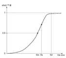
도 3은 일실시예에 따른 PUF(120)의 구성을 설명하기 위한 그래프이다.3 is a graph illustrating a configuration of the
그래프에서 비아의 사이즈가 커질수록, 메탈 레이어들 사이의 단락(Short) 확률이 1에 가까운 것을 확인할 수 있다. 디자인 룰에 따른 비아 사이즈는 Sd로서, 메탈 레이어들 사이의 단락이 충분히 보장되는 값이다.As the size of the via increases in the graph, it can be seen that the short probability between the metal layers is closer to one. The via size according to the design rule is Sd, a value at which a short between the metal layers is sufficiently guaranteed.
그리고, SM은 이론적으로 메탈 레이어의 단락 확률이 0.5가 되는 비아 사이즈인데, 상기한 바와 같이, 공정에 따라 값이 상이하며 실험에 의해 최대한 비슷한 값을 찾을 수는 있지만, 정확한 SM을 찾는 것은 어렵다.And, SM is theoretically inde a short circuit probability of the metal layer, the via size is 0.5, as described above, by the value of different and each experiment depending on the process to find the most similar values, but, finding the correct SM it's difficult.
따라서, 일실시예에 따른 PUF(120)에서는 구체적인 실험에 따라 메탈 레이어들 사이의 단락 여부가 0.5에서 미리 지정된 허용 오차를 갖는 Sx1과 Sx2 범위 내(상기 Sx1 과 Sx2는 별도로 도시하지 않지만, 도시된 Sx 근처의 일정한 마진을 갖는 영역임)에서 설정될 수 있다.Accordingly, in the
도 4는 다른 일실시예에 따른 PUF(120)의 구성을 설명하기 위한 개념도이다.4 is a conceptual diagram illustrating a configuration of the
본 실시예에 따르면, 메탈 라인들 사이의 간격을 조정하여 메탈 라인들 사이의 오픈 여부가 확률적으로 결정되도록 할 수 있다.According to the present exemplary embodiment, the gap between the metal lines may be adjusted to determine whether the metal lines are open.
메탈 라인들 사이의 간격을 충분히 작게 한 그룹(410)에서는 모든 경우에서 메탈 라인들이 단락되었다.In the
그리고, 메탈 라인 간격을 매우 크게 한 그룹(430)에서는 모든 경우에서 메탈 라인들이 단락되지 않았다.In the
본 실시예에 따른 PUF(120)에서는, 그룹(420)과 같이, 메탈 라인들 중 일부는 단락되고 일부는 단락되지 않도록, 단락이 확률적으로 이루어지는 메탈 라인 간격을 설정한다.In the
도 5는 일실시예에 따른 PUF(120)에서 유니크 키를 생성할 수 있도록 하는 인터-레이어 컨택 어레이를 도시한다.5 illustrates an inter-layer contact array that enables the generation of a unique key in
반도체 기판(substrate)에 적층된 메탈 레이어들 사이에 가로 M개, 세로 N 개(단, M 및 N은 자연수), 총 M*N 개의 비아가 형성된 모습이 도시되었다.M and N vias (where M and N are natural numbers) and a total of M * N vias are formed between the metal layers stacked on the semiconductor substrate.
PUF(120)는 M*N 개의 비아들 각각이 메탈 레이어들 사이를 단락시키는지(디지털 값 0) 또는 단락시키지 못하는지(디지털 값 1)의 여부에 따라, M*N 비트(bit)의 디지털 값인 유니크 키를 생성한다.The
그리고, 이렇게 생성된 M*N 비트의 유니크 키는 암호화부(130)가 사용자 입력 패스워드 및/또는 바이오 정보를 등록하는 과정에서 암호화를 수행하는 데에 시드 키(Seed key)로서 이용될 수 있다.In addition, the generated M * N bit unique key may be used as a seed key for the
도 6은 일실시예에 따라 PUF(120)가 생성한 유니크 키를 인식하는 과정을 설명하기 위한 도면이다.6 is a diagram for describing a process of recognizing a unique key generated by the
본 실시예에 따르면, PUF(120)에 포함된 어느 하나의 노드에서, 레퍼런스 전압 VDD와 그라운드(ground) 사이에 있는 리드 트랜지스터가 상기 노드의 단락 여부를 검사한다.According to the present embodiment, at any one node included in the
풀다운(Pull-down) 회로로 구성되는 도 6의 실시예에서, PUF(120) 내의 하나의 노드, 이를테면 비아가 메탈 레이어들 사이를 단락시키면 출력 값은 0으로 되고, 그렇지 않으면 출력 값이 1로 된다. 이러한 과정을 통해 PUF(120)가 생성한 유니크 키가 판독될 수 있다. 한편, 본 명세서에서 별다른 언급이 없더라도 풀다운 회로에 대한 설명은 풀업(Pull-up) 회로로 구성되는 예로 확장될 수 있고, 이는 이 기술이 속하는 기술 분야에서는 자명한 것이므로 구체적인 언급이 없더라도 다른 다양한 실시예를 제외하는 것으로 이해되어서는 안 된다.In the embodiment of FIG. 6, which consists of a pull-down circuit, if one node in the
또한, 메탈 라인들 사이의 단락을 이용하는 실시예도 동일하게 식별키가 생성된다.In addition, an embodiment using a short circuit between metal lines also generates an identification key.
나아가, 이러한 디지털 값 판독 과정은 일부 실시예에 불과하며, 다른 실시예들에 의한 디지털 값 판독 역시 가능하다.Furthermore, this digital value reading process is only a few embodiments, and digital value reading by other embodiments is also possible.
따라서, PUF(120) 내의 메탈 레이어 간 또는 메탈 라인 간의 단락 여부를 검사하여 디지털 값을 판독할 수 있는 구성이라면, 본 발명의 사상을 벗어나지 않는 범위에서 다른 변형이 가능하며, 이러한 구성 또한 본 발명의 범위에서 배제되지 않는다.Therefore, if the configuration is capable of reading a digital value by checking whether there is a short circuit between metal layers or metal lines in the
도 7은 일실시예에 따라 PUF가 생성한 유니크 키의 밸런싱 과정을 설명하기 위한 개념도이다.7 is a conceptual diagram illustrating a balancing process of a unique key generated by a PUF according to an embodiment.
본 실시예에 따르면, PUF(120)가 생성한 M*N 비트의 디지털 값은 미리 설정된 개수로 묶여서 그룹핑될 수 있다.According to the present embodiment, the digital values of the M * N bits generated by the
도시된 실시예서는, 4 개의 디지털 값이 하나의 그룹으로 그룹핑 되었다.In the illustrated embodiment, four digital values are grouped into one group.
이렇게 복수 개의 디지털 값 그룹이 생성되면, 개별 그룹들의 디지털 값을 비교함으로써 디지털 값 '0'과 디지털 값 '1' 사이의 밸런싱이 수행된다.When a plurality of digital value groups are generated as described above, balancing between digital values '0' and digital values '1' is performed by comparing digital values of individual groups.
이를테면, 그룹(710)과 그룹(720)가 각각 생성한 4비트의 디지털 값의 크기를 비교한다. 그리고, 그룹(710)의 4비트 디지털 값이 그룹(720)의 4비트 디지털 값보다 크면, 상기 그룹(710)과 그룹(720)을 대표하는 디지털 값은 1로 결정한다.For example, the sizes of the 4-bit digital values generated by the
반대로, 그룹(710)의 4비트 디지털 값이 그룹(720)의 4비트 디지털 값보다 작으면, 상기 그룹(710)과 그룹(720)을 대표하는 디지털 값은 0으로 결정한다.Conversely, if the 4-bit digital value of the
물론, 그룹(720)의 4비트 디지털 값이 그룹(710)의 4비트 디지털 값보다 큰 경우에, 대표 디지털 값을 1로 결정할 수도 있다.Of course, when the 4-bit digital value of the
만일, 그룹(710)의 4비트 디지털 값과 그룹(720)의 4비트 디지털 값이 같을 경우에는, 대표 디지털 값을 1 또는 0으로 결정하거나, 아니면, 대표 값을 결정하지 않을 수도 있다.If the 4-bit digital value of the
PUF(120) 내의 복수 개의 노드들 각각에서는 전도성 레이어들 사이가 단락되는 비율(디지털 값 0)과 단락되지 않는 비율(디지털 값 1)이 서로 달라서, 0과 1의 밸런싱(balancing)이 맞추어지지 않는 경우도 있을 수 있다.In each of the plurality of nodes in the
하나의 그룹 내에서는 각 비트의 값이 1일 확률과 0일 확률이 다를 수 있지만, 서로 다른 그룹을 비교하면 어느 그룹의 디지털 값이 큰 지는 50%의 확률이 될 수 있다. 이를테면, 두 개의 그룹들(710 및 720) 중 어느 한 그룹이 다른 한 그룹보다 큰 디지털 값을 가질 확률은 50%이다. 따라서, 상기한 과정을 통해서 0과 1의 확률적 밸런싱이 보장되는 것으로 이해될 수 있다.In one group, each bit may have a probability of 1 and a probability of 0, but when comparing different groups, there may be a 50% probability of which group's digital value is large. For example, the probability that either one of the two
또한, 그룹(730)과 그룹(740)을 비교하여 또 다른 디지털 값 1비트가 생성될 수 있어서, 그룹(710 내지 740)을 통해 최소 2 비트 이상의 유니크 키가 제공될 수 있다.In addition, another
이러한 과정에 의해, PUF(120)가 생성한 디지털 값의 밸런싱이 수행되면 PUF(120)가 생성한 디지털 값인 유니크 키의 무작위성은 더욱 높은 수준으로 보장될 수 있다.By this process, when balancing of the digital value generated by the
상기한 바에 따라, 원래 생성된 디지털 값이 M*N 비트였다면, 상기 도 7에서 PUF(120)에서 생성된 최종 디지털 값은 (M*N/8) 비트일 수 있다. 도 7의 실시예에서는 8 비트의 디지털 값을 이용하여 새로운 1 비트의 디지털 값을 결정하기 때문이다.As described above, if the originally generated digital value was M * N bits, the final digital value generated by the
따라서, 상기 실시예에 의하면, 무작위성과 시불변성을 동시에 만족할 수 있는 신뢰 가능한 유니크 키가 PUF(120)에 의해 생성된다.Thus, according to this embodiment, the
일실시예에 따르면, 암호화부(130)는 이렇게 밸런싱 된 유니크 키를 이용하여 사용자 입력 패스워드 및/또는 바이오 정보를 암호화 할 수 있다.According to an embodiment of the present disclosure, the
이렇게 PUF(120)에 의해 유니크 키가 생성되는 경우, 제조 비용이 낮으면서 시불변성도 만족되고, 나아가 암호화부(130)가 AES 등의 방법으로 패스워드를 암호화하는 시드가 되는 유니크 키는 외부로 유출되지 않는다.When the unique key is generated by the
도 8은 다른 일실시예에 따른 정보 처리 장치를 도시한다.8 illustrates an information processing apparatus according to another embodiment.
본 실시예에서는 정보 처리 장치(800)의 암호화부(820) 내에 N 개(단, N은 자연수)의 PUF들(830)이 포함될 수 있다.In the present exemplary embodiment, N PUFs 830 (where N is a natural number) may be included in the
N 개의 PUF들(830)은 반도체 제조 과정에서 암호화부(820) 내에 포함되어 숨겨질(hided) 수 있다.The
이를 테면, 암호화부(820) 내에는 적어도 하나의 PUF들, 이를테면 도 9에서 도시되는 PUF들(831, 832, 833, 834 및 835 등)이 포함된다.For example, the
예시적으로 도 9에 도시된 PUF들(831, 832, 833, 834 및 835 등)은 각각 독립적으로 또는 상호 연관하여, 수신부(810)에서 수신된 패스워드 및/또는 바이오 정보를 AES 또는 T-DES 등의 방식으로 암호화하는 데에 사용되는 시드(seed) 유니크 키를 생성한다.For example, the
일부 실시예에서는 암호화부(820) 내에 PUF가 하나만 포함될 수도 있으나, 다른 실시예들에서는 도 9에 도시된 바와 같이 복수 개 포함된다.In some embodiments, only one PUF may be included in the
그리고, 이렇게 복수 개의 PUF들이 포함된 실시예에서는 암호화부(820) 내에 PUF 선택부(840)가 더 포함될 수 있다.In an embodiment in which a plurality of PUFs are included, the
PUF 선택부(840)는 복수 개의 PUF들(831, 832, 833, 834 및 835 등) 중 적어도 하나를 선택하여 암호화부(820)가 사용자 입력 패스워드 및/또는 바이오 정보를 암호화하는 데에 이용될 실제 PUF를 적어도 하나 선택한다.The
암호화부(820)가 생성한 식별키가 저장부(850)에 저장될 수 있는 과정 및 저장부(850)의 구현은 도 1의 실시예와 동일하다.The process in which the identification key generated by the
또한, 인증부(860)가 인증을 위해 입력된 사용자 패스워드 및/또는 바이오 정보를 미리 등록된 식별키와 비교하여 인증을 수행하는 내용도 도 1에서 설명한 바와 같다.In addition, as described above with reference to FIG. 1, the
도 9는 일실시예에 따라 PUF들이 암호화부 내에 배치되는 예시적 구성을 도시한다.9 illustrates an example configuration in which PUFs are disposed in an encryption unit according to an embodiment.
암호화부(820)가 설계되어 제조되는 과정에서, PUF들(831, 832, 833, 834 및 835 등)이 암호화부(820) 내에 숨겨져서(hided), 외부에서는 이러한 PUF들(831, 832, 833, 834 및 835 등)의 위치나 역할에 대해 분석할 수 없다. 즉, 각각의 PUF들(831, 832, 833, 834 및 835 등)의 위치도 파악하기 힘들뿐더러, 어느 PUF가 실제 암호화부(820)에 의해 암호화 시드 키로서 이용되는지도 파악할 수 없다.In the process in which the
따라서, PUF들(831, 832, 833, 834 및 835 등)을 통한 암호화부(820) 동작의 암호화 과정은 외부에서 분석이 불가능하며, 암호화부(820)가 다른 구성들과 통신하는 버스(bus)를 프로빙(probing)하더라도 유니크 키를 알아내는 것이 불가능하다.Therefore, the encryption process of the operation of the
결국, 사용자가 입력한 패스워드 및/또는 바이오 정보가 암호화부(820)에 의해 암호화되는 과정은 높은 수준으로 보안이 유지될 수 있다.As a result, a process in which the password and / or bio information input by the user is encrypted by the
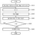
도 10은 일실시예에 따른 정보 처리 방법에 따라 패스워드 및/또는 바이오 정보를 암호화 하여 저장(등록)하는 과정을 도시하는 흐름도이다.10 is a flowchart illustrating a process of encrypting and storing (registering) a password and / or bio information according to an information processing method according to an embodiment.
도 1을 참조하면, 단계(1010)에서 정보 처리 장치(100)의 수신부(110)에 사용자 입력 패스워드 및/또는 바이오 정보가 수신된다. 수신된 패스워드 및/또는 바이오 정보는 상기한 바와 같이 지식 기반 인증을 구현할 수 있다.Referring to FIG. 1, in
단계(1020)에서는 상기 패스워드 및/또는 바이오 정보가 AES 또는 T-DES 등의 방법에 의해 암호화되는 과정에서, 반복되는 N 번(단, N은 자연수)의 이터래이션(iteration)을 위해 초기값이 i=0에서 i를 1 증가시킨다.In
그리고, 단계(1030)에서 PUF(120)가 제공하는 유니크 키가 독출되고, 단계(1040)에서는 i 번째 이터래이션이 수행되어, 키 ID(i)이 생성된다.In
그리고, 단계(1050)에서는 i가 N이 될 때까지 상기 이터래이션을 진행시킨다.In
이렇게 N 회 이터래이션에 걸쳐, 암호화부(120)는 최종 식별키인 키 ID(N)을 생성하며, 단계(1060)에서는 생성된 식별키 ID(N)이 저장부(140)에 저장된다.In this way, the
도 11은 도 8의 실시예에 따른 정보 처리 장치가 패스워드 및/또는 바이오 정보를 암호화 하여 저장하는 과정을 도시하는 흐름도이다.FIG. 11 is a flowchart illustrating a process of encrypting and storing a password and / or bio information by an information processing apparatus according to the embodiment of FIG. 8.
단계(1110)에서 패스워드가 수신되고 이터래이션 i의 초기 값이 0으로 설정되는 과정은 도 10의 실시예와 같다.In
그리고, i의 값이 1 증가되며(단계 1120), 도 8 및 도 9를 참조하여 설명된 복수 개의 PUF들(831, 832, 833, 834 및 835 등) 중 어느 하나가 PUF 선택부(840)에 의해 선택된다.Then, the value of i is increased by 1 (step 1120), and any one of the plurality of
일부 실시예에서는 이러한 선택이 매 이터래이션 마다 새로이 수행될 수도 있으며, 다른 실시예에서는 선택 과정이 한 번만 수행될 수도 있다.In some embodiments, this selection may be newly performed for every acquisition, and in other embodiments, the selection process may be performed only once.
선택된 PUF가 제공하는 디지털 값을 이용하여 i 번째 이터래이션에서의 식별키 ID(i)가 생성되며(단계 1140), 단계(1150)에 의해 이터래이션이 N 회 반복된다.Using the digital value provided by the selected PUF, an identification key ID (i) in the i-th iteration is generated (step 1140), and the iteration is repeated N times by
이렇게 N 번 암호화부(820)의 암호화가 수행되면 식별키 ID(N)이 생성되며, 단계(1160)에서는 생성된 키 ID(N)가 저장부(850)에 저장된다.When the encryption of the N-
도 12는 일실시예에 따른 정보 처리 장치에서 사용자 입력 패스워드 및/또는 바이오 정보를 인증하는 과정을 도시하는 흐름도이다.12 is a flowchart illustrating a process of authenticating a user input password and / or bio information in an information processing apparatus according to an embodiment.
도 10 내지 도 11의 실시예들은, 각각 정보 처리 장치(100) 또는 정보 처리 장치(800)가 인증에 사용할 패스워드 및/또는 바이오 정보를 최초 등록하는 내용에 연관되었다면, 도 12는 상기 패스워드 및/또는 바이오 정보가 암호화되어 등록된 이후 실제 인증 수행 과정에 연관될 수 있다.10 to 11, if the
일실시예에 따라, 단계(1210)에서, 사용자가 인증 수행을 위해 입력하는 패스워드 및/또는 바이오 정보가 수신부(110 또는 810)에 입력될 수 있다.According to an embodiment, in
그러면, 단계(1220)에서, 암호화부(130 또는 820)는 PUF가 생성한 유니크 키를 이용하여 상기 입력된 패스워드 및/또는 바이오 정보를 암호화하여 암호화된 패스워드 및/또는 바이오 정보를 인증부(150 또는 860)에 전달할 수 있다.Then, in
그러면, 인증부(150 또는 860)는 상기 암호화된 패스워드 및/또는 바이오 정보가 저장부(140 또는 850)에 미리 저장되어 있는 등록된 식별키와 일치하는 지의 여부를 판단하여 패스워드 및/또는 바이오 정보의 인증 성공 또는 인증 실패를 결정할 수 있다.Then, the
도 13은 다른 일실시예에 따른 정보 처리 장치에서 사용자 입력 패스워드 및/또는 바이오 정보를 인증하는 과정을 도시하는 흐름도이다.13 is a flowchart illustrating a process of authenticating a user input password and / or bio information in an information processing apparatus according to another embodiment.
단계(1310)에서, 사용자가 인증 수행을 위해 입력하는 패스워드 및/또는 바이오 정보가 수신부(110 또는 810)에 입력될 수 있다. 수신부(110 또는 810)는 입력된 패스워드 및/또는 바이오 정보를 인증부(150 또는 860)에 전달한다.In
단계(1320)에서, 그리고 암호화부(130 또는 820)는 저장부(140 또는 850)에 미리 저장되어 있는 식별키 ID(N)을 복호화 하여 복호화된 식별키를 인증부(150 또는 860)에 전달할 수 있다.In
그러면, 단계(1330)에서, 인증부(150 또는 860)는 상기 수신부(110 또는 810)로부터 전달된 사용자 입력 패스워드 및/또는 바이오 정보와 상기 암호화부(130 또는 820)로부터 전달된 복호화된 식별키가 일치하는 지의 여부를 판단하여 패스워드 및/또는 바이오 정보의 인증 성공 또는 인증 실패를 결정할 수 있다.Then, in
도 1을 참조하여 상술한 바와 같이, 도 13의 실시예는 바이오 정보의 처리에 유용할 수 있다. 바이오 정보, 이를테면 지문이나 홍채 무늬는 입력 시 마다 식별 오차가 있을 수 있어서, 등록 시에 사용된 동일한 오브젝트의 바이오 정보를 추후에 인증 수행 시 다시 입력하더라도, 식별되는 바이오 정보는 완전히 일치하지 않을 수도 있다. 따라서, 통상적인 바이오 정보의 인증 과정도 입력된 바이오 정보와 미리 등록된 바이오 정보의 일치도를 판단하고 있다.As described above with reference to FIG. 1, the embodiment of FIG. 13 may be useful for processing bioinformation. Bioinformation, such as fingerprints or iris patterns, may have an identification error for each input, so even if bioinformation of the same object used at the time of registration is re-entered later during authentication, the identified bioinformation may not be completely identical. . Therefore, the normal bio information authentication process also determines the degree of correspondence between the input bio information and the previously registered bio information.
도 13의 실시예에서도, 인증을 위해 입력되어 수신부(110 또는 810)에 전달된 바이오 정보를 암호화한 결과를 미리 등록된 식별키와 비교 하지 않고, 대신 미리 등록된 식별키를 복호화 하여, 상기 바이오 정보와의 일치도에 따라 인증 성공 또는 인증 실패를 결정할 수 있다.In the embodiment of FIG. 13, the biometric information input for authentication and transmitted to the receiving
상술한 다양한 실시예들에 따르면, 인증을 위해 사용되는 사용자 패스워드 및/또는 바이오 정보가 안전하게 암호화되어 관리될 수 있다. 또한, 인증 수행에 있어서, 사용자 입력 패스워드 및/또는 바이오 정보뿐만 아니라 디바이스에 임베디드된 PUF의 유니크 키가 이용되기 때문에, 인증의 신뢰성이 높은 수준으로 제공될 수 있다.According to the various embodiments described above, the user password and / or bio information used for authentication can be securely encrypted and managed. In addition, in performing authentication, a unique key of the PUF embedded in the device as well as the user input password and / or bio information is used, so that the reliability of the authentication can be provided at a high level.
본 발명의 일 실시예에 따른 방법은 다양한 컴퓨터 수단을 통하여 수행될 수 있는 프로그램 명령 형태로 구현되어 컴퓨터 판독 가능 매체에 기록될 수 있다. 상기 컴퓨터 판독 가능 매체는 프로그램 명령, 데이터 파일, 데이터 구조 등을 단독으로 또는 조합하여 포함할 수 있다. 상기 매체에 기록되는 프로그램 명령은 본 발명을 위하여 특별히 설계되고 구성된 것들이거나 컴퓨터 소프트웨어 당업자에게 공지되어 사용 가능한 것일 수도 있다. 컴퓨터 판독 가능 기록 매체의 예에는 하드 디스크, 플로피 디스크 및 자기 테이프와 같은 자기 매체(magnetic media), CD-ROM, DVD와 같은 광기록 매체(optical media), 플롭티컬 디스크(floptical disk)와 같은 자기-광 매체(magneto-optical media), 및 롬(ROM), 램(RAM), 플래시 메모리 등과 같은 프로그램 명령을 저장하고 수행하도록 특별히 구성된 하드웨어 장치가 포함된다. 프로그램 명령의 예에는 컴파일러에 의해 만들어지는 것과 같은 기계어 코드뿐만 아니라 인터프리터 등을 사용해서 컴퓨터에 의해서 실행될 수 있는 고급 언어 코드를 포함한다. 상기된 하드웨어 장치는 본 발명의 동작을 수행하기 위해 하나 이상의 소프트웨어 모듈로서 작동하도록 구성될 수 있으며, 그 역도 마찬가지이다.The method according to an embodiment of the present invention can be implemented in the form of a program command which can be executed through various computer means and recorded in a computer-readable medium. The computer readable medium may include program instructions, data files, data structures, etc. alone or in combination. The program instructions recorded on the medium may be those specially designed and constructed for the present invention or may be available to those skilled in the art of computer software. Examples of computer-readable recording media include magnetic media such as hard disks, floppy disks, and magnetic tape, optical media such as CD-ROMs, DVDs, and magnetic disks, such as floppy disks. Magneto-optical media, and hardware devices specifically configured to store and execute program instructions, such as ROM, RAM, flash memory, and the like. Examples of program instructions include not only machine code generated by a compiler, but also high-level language code that can be executed by a computer using an interpreter or the like. The hardware device described above may be configured to operate as one or more software modules to perform the operations of the present invention, and vice versa.
이상과 같이 본 발명은 비록 한정된 실시예와 도면에 의해 설명되었으나, 본 발명은 상기의 실시예에 한정되는 것은 아니며, 본 발명이 속하는 분야에서 통상의 지식을 가진 자라면 이러한 기재로부터 다양한 수정 및 변형이 가능하다.As described above, the present invention has been described by way of limited embodiments and drawings, but the present invention is not limited to the above embodiments, and those skilled in the art to which the present invention pertains various modifications and variations from such descriptions. This is possible.
그러므로, 본 발명의 범위는 설명된 실시예에 국한되어 정해져서는 아니 되며, 후술하는 특허청구범위뿐 아니라 이 특허청구범위와 균등한 것들에 의해 정해져야 한다.Therefore, the scope of the present invention should not be limited to the described embodiments, but should be determined by the equivalents of the claims, as well as the claims.
Claims (23)
Translated fromKorean상기 유니크 키를 이용하여 사용자로부터 수신한 패스워드를 암호화하여 식별키를 생성하는 암호화부
를 포함하고,
상기 PUF는 반도체의 전도성 레이어 사이에 형성되는 인터-레이어 컨택이 상기 전도성 레이어를 단락 하는지의 여부를 이용하여 상기 유니크 키를 생성하는, 정보 처리 장치.A physically unclonable function (PUF) for generating at least one unique key using process variations in a semiconductor manufacturing process; And
Encryption unit for generating an identification key by encrypting the password received from the user using the unique key
Lt; / RTI >
And the PUF generates the unique key using whether an inter-layer contact formed between the conductive layers of the semiconductor shorts the conductive layer.
상기 반도체의 전도성 레이어 사이에 형성되는 상기 인터-레이어 컨택은, 상기 반도체 제조 공정에서 제공되는 디자인 룰에 따른 사이즈 보다 작도록 구성되는, 정보 처리 장치.3. The method of claim 2,
The inter-layer contact formed between the conductive layers of the semiconductor is configured to be smaller than the size according to the design rules provided in the semiconductor manufacturing process.
상기 PUF는, 상기 반도체의 전도성 레이어 사이에 형성되는 상기 인터-레이어 컨택이 상기 전도성 레이어를 단락 하는 확률과 단락 하지 못하는 확률의 차이가 미리 지정된 오차 범위 내에 있도록 하는 상기 인터-레이어 컨택의 사이즈를 갖는, 정보 처리 장치.3. The method of claim 2,
The PUF has a size of the inter-layer contact such that a difference between a probability that the inter-layer contact formed between the conductive layers of the semiconductor shorts the conductive layer and a probability of not shorting is within a predetermined error range. Information processing device.
상기 유니크 키를 이용하여 사용자로부터 수신한 패스워드를 암호화하여 식별키를 생성하는 암호화부
를 포함하고,
상기 PUF는, 한 쌍의 전도성 레이어와 그 사이를 연결하는 하나의 인터-레이어 컨택을 이용하여 1 비트의 디지털 값을 생성하는 단위 구조를 N 개 가져서 - 단, N은 자연수임 -, 상기 N 개의 단위 구조를 통해 N 비트의 유니크 키를 생성하는, 정보 처리 장치.A physically unclonable function (PUF) for generating at least one unique key using process variations in a semiconductor manufacturing process; And
Encryption unit for generating an identification key by encrypting the password received from the user using the unique key
Lt; / RTI >
The PUF has N unit structures that generate a 1-bit digital value using a pair of conductive layers and one inter-layer contact therebetween, where N is a natural number, wherein N is a natural number. An information processing apparatus, generating a unique key of N bits through a unit structure.
상기 PUF는 N 비트의 디지털 값을 생성하고,
상기 정보 처리 장치는 상기 N 비트의 유니크 키에 포함된 디지털 값들을 k 개 단위로 그룹핑 하고 - 단, k는 자연수임 -, 그룹핑된 복수 개의 그룹들 중 제1 그룹 및 제2 그룹을 비교하여, 상기 제1 그룹에 포함된 k개의 디지털 비트로 구성된 값이 상기 제2 그룹에 포함된 k개의 디지털 비트로 구성된 값보다 큰 경우에 상기 제1 그룹과 상기 제2 그룹을 대표하는 디지털 값을 1로 결정하는, 정보 처리 장치.The method of claim 5,
The PUF generates a digital value of N bits,
The information processing apparatus groups the digital values included in the N-bit unique key by k units, where k is a natural number, and compares the first group and the second group of the plurality of grouped groups. When the value consisting of k digital bits included in the first group is greater than the value consisting of k digital bits included in the second group, a digital value representing the first group and the second group is determined as 1 Information processing device.
상기 정보 처리 장치는, 상기 제1 그룹에 포함된 k개의 디지털 비트로 구성된 값이 상기 제2 그룹에 포함된 k개의 디지털 비트로 구성된 값이 같은 경우, 설정에 따라 선택적으로, 상기 제1 그룹과 상기 제2 그룹의 대표하는 디지털 값을 1 또는 0 중 어느 한 쪽으로 결정하거나 또는 상기 제1 그룹과 상기 제2 그룹의 대표하는 디지털 값을 결정하지 않는, 정보 처리 장치.The method according to claim 6,
The information processing apparatus, if the value composed of k digital bits included in the first group is the same as the value composed of k digital bits included in the second group, is selectively set according to a setting. The information processing apparatus which does not determine the representative digital value of two groups to either 1 or 0, or does not determine the representative digital value of the said 1st group and said 2nd group.
상기 유니크 키를 이용하여 사용자로부터 수신한 패스워드를 암호화하여 식별키를 생성하는 암호화부
를 포함하고,
상기 암호화부는, 상기 유니크 키를 라운드 키로 사용하여 상기 패스워드를 N 회 - N은 자연수 - 암호화하여 상기 식별키를 생성하는 정보 처리 장치.A physically unclonable function (PUF) for generating at least one unique key using process variations in a semiconductor manufacturing process; And
Encryption unit for generating an identification key by encrypting the password received from the user using the unique key
Lt; / RTI >
And the encryption unit generates the identification key by encrypting the password N times-N is a natural number-using the unique key as a round key.
상기 암호화부는, AES 방법 또는 T-DES 방법으로 상기 패스워드를 암호화하여 상기 식별키를 생성하는 정보 처리 장치.9. The method of claim 8,
And the encryption unit generates the identification key by encrypting the password by an AES method or a T-DES method.
상기 유니크 키를 이용하여 입력된 바이오 정보를 암호화하여 식별키를 생성하는 암호화부
를 포함하고,
상기 PUF는 반도체의 전도성 레이어 사이에 형성되는 인터-레이어 컨택이 상기 전도성 레이어를 단락 하는지의 여부를 이용하여 상기 유니크 키를 생성하는, 정보 처리 장치.A physically unclonable function (PUF) for generating at least one unique key using process variations in a semiconductor manufacturing process; And
Encryption unit for generating the identification key by encrypting the input bio information using the unique key
Lt; / RTI >
And the PUF generates the unique key using whether an inter-layer contact formed between the conductive layers of the semiconductor shorts the conductive layer.
상기 반도체의 전도성 레이어 사이에 형성되는 상기 인터-레이어 컨택은, 상기 반도체 제조 공정에서 제공되는 디자인 룰에 따른 사이즈 보다 작도록 구성되는, 정보 처리 장치.12. The method of claim 11,
The inter-layer contact formed between the conductive layers of the semiconductor is configured to be smaller than the size according to the design rules provided in the semiconductor manufacturing process.
상기 PUF는, 상기 반도체의 전도성 레이어 사이에 형성되는 상기 인터-레이어 컨택이 상기 전도성 레이어를 단락 하는 확률과 단락 하지 못하는 확률의 차이가 미리 지정된 오차 범위 내에 있도록 하는 상기 인터-레이어 컨택의 사이즈를 갖는, 정보 처리 장치.12. The method of claim 11,
The PUF has a size of the inter-layer contact such that a difference between a probability that the inter-layer contact formed between the conductive layers of the semiconductor shorts the conductive layer and a probability of not shorting is within a predetermined error range. Information processing device.
를 포함하고,
상기 암호화부는, 상기 적어도 하나의 유니크 키를 라운드 키로 사용하여 상기 패스워드 또는 상기 바이오 정보 중 적어도 하나를 N 회 - N은 자연수 - 암호화하여 상기 식별키를 생성하는 정보 처리 장치.At least one unique key provided by at least one of the at least one PUF, including at least one PUF (Physically Unclonable Function) for generating a unique key composed of at least one digital value using process variations in a semiconductor manufacturing process Encryption unit for generating an identification key by encrypting at least one of a password or bio information received from the user using
Lt; / RTI >
And the encryption unit generates the identification key by encrypting at least one of the password or the bio information N times-N is a natural number-using the at least one unique key as a round key.
상기 암호화부는, AES 방법 또는 T-DES 방법으로 상기 패스워드 또는 상기 바이오 정보 중 적어도 하나를 암호화하여 상기 식별키를 생성하는 정보 처리 장치.16. The method of claim 15,
And the encryption unit generates the identification key by encrypting at least one of the password or the bio information by an AES method or a T-DES method.
를 포함하고,
상기 적어도 하나의 PUF 각각은 반도체의 전도성 레이어 사이에 형성되는 인터-레이어 컨택이 상기 전도성 레이어 사이를 단락 하는지의 여부를 이용하여 상기 유니크 키를 생성하는, 정보 처리 장치.At least one unique key provided by at least one of the at least one PUF, including at least one PUF (Physically Unclonable Function) for generating a unique key composed of at least one digital value using process variations in a semiconductor manufacturing process Encryption unit for generating an identification key by encrypting at least one of a password or bio information received from the user using
Lt; / RTI >
Wherein each of the at least one PUF generates the unique key using whether an inter-layer contact formed between the conductive layers of the semiconductor shorts between the conductive layers.
상기 인터-레이어 컨택은, 상기 반도체 제조 공정에서 제공되는 디자인 룰에 따른 사이즈 보다 작도록 구성되는, 정보 처리 장치.18. The method of claim 17,
And the inter-layer contact is configured to be smaller than a size according to a design rule provided in the semiconductor manufacturing process.
상기 PUF는, 상기 반도체의 전도성 레이어 사이에 형성되는 상기 인터-레이어 컨택이 상기 전도성 레이어를 단락 하는 확률과 단락 하지 못하는 확률의 차이가 미리 지정된 오차 범위 내에 있도록 하는, 상기 인터-레이어 컨택의 사이즈를 갖는, 정보 처리 장치.18. The method of claim 17,
The PUF is configured to determine the size of the inter-layer contact so that a difference between a probability that the inter-layer contact formed between the conductive layers of the semiconductor shorts the conductive layer and a probability of not shorting is within a predetermined error range. It has an information processing apparatus.
상기 적어도 하나의 PUF 중 상기 암호화부가 상기 암호화에 이용할 PUF를 선택하는 PUF 선택부
를 포함하는, 정보 처리 장치.At least one unique key provided by at least one of the at least one PUF, including at least one PUF (Physically Unclonable Function) for generating a unique key composed of at least one digital value using process variations in a semiconductor manufacturing process An encryption unit for generating an identification key by encrypting at least one of a password or bio information received from a user; And
PUF selector for selecting the PUF to be used for the encryption unit of the at least one PUF encryption
And the information processing apparatus.
상기 정보 처리 장치의 암호화부가, 상기 유니크 키를 이용하여, 상기 정보 처리 장치에 입력된 제1 사용자 입력 패스워드 또는 제1 사용자 바이오 정보 중 적어도 하나를 암호화하여 암호화된 패스워드 또는 암호화된 바이오 정보 중 적어도 하나를 생성하는 단계;
사용자로부터 상기 정보 처리 장치에 제2 사용자 입력 패스워드 또는 제2 사용자 바이오 정보 중 적어도 하나가 입력되는 경우, 상기 제2 사용자 입력 패스워드 또는 상기 제2 사용자 바이오 정보 중 적어도 하나를 암호화하는 단계; 및
상기 정보 처리 장치의 인증부가, 암호화된 상기 제2 사용자 입력 패스워드 또는 암호화된 상기 제2 사용자 바이오 정보 중 적어도 하나를 상기 암호화된 패스워드 또는 상기 암호화된 바이오 정보 중 적어도 하나와 비교하여 인증을 수행하는 단계
를 포함하는, 정보 처리 방법.Generating, by the PUF (Physically Unclonable Function) included in the information processing apparatus, at least one unique key by using the process deviation in the semiconductor manufacturing process;
At least one of an encrypted password or encrypted bio information by encrypting at least one of a first user input password or first user bio information input to the information processing device using the unique key, by the encryption unit of the information processing device. Generating a;
Encrypting at least one of the second user input password or the second user bio information when a user inputs at least one of a second user input password or second user bio information to the information processing apparatus; And
Authenticating, by the authentication unit of the information processing apparatus, comparing at least one of the encrypted second user input password or the encrypted second user bio information with at least one of the encrypted password or the encrypted bio information;
And an information processing method.
상기 정보 처리 장치의 암호화부가, 상기 유니크 키를 이용하여, 상기 정보 처리 장치에 입력된 제1 사용자 입력 패스워드 또는 제1 사용자 바이오 정보 중 적어도 하나를 암호화하여 암호화된 패스워드 또는 암호화된 바이오 정보 중 적어도 하나를 생성하는 단계;
사용자로부터 상기 정보 처리 장치에 제2 사용자 입력 패스워드 또는 제2 사용자 바이오 정보 중 적어도 하나가 입력되는 경우, 상기 정보 처리 장치의 암호화부가 상기 암호화된 패스워드 또는 상기 암호화된 바이오 정보 중 적어도 하나를 복호화하여 상기 제1 사용자 입력 패스워드 또는 상기 제1 사용자 바이오 정보 중 적어도 하나를 생성하는 단계; 및
상기 정보 처리 장치의 인증부가, 상기 복호화된 상기 제1 사용자 패스워드 또는 상기 제1 사용자 바이오 정보 중 적어도 하나를, 상기 제2 사용자 입력 패스워드 또는 상기 제2 사용자 바이오 정보 중 적어도 하나와 비교하여 인증을 수행하는 단계
를 포함하는, 정보 처리 방법.Generating, by the PUF (Physically Unclonable Function) included in the information processing apparatus, at least one unique key by using the process deviation in the semiconductor manufacturing process;
At least one of an encrypted password or encrypted bio information by encrypting at least one of a first user input password or first user bio information input to the information processing device using the unique key, by the encryption unit of the information processing device. Generating a;
When at least one of a second user input password or second user bio information is input from the user to the information processing apparatus, the encryption unit of the information processing apparatus decrypts at least one of the encrypted password or the encrypted bio information to perform the operation. Generating at least one of a first user input password or the first user bio information; And
The authentication unit of the information processing device performs authentication by comparing at least one of the decrypted first user password or the first user bio information with at least one of the second user input password or the second user bio information. Steps to
And an information processing method.
Priority Applications (12)
| Application Number | Priority Date | Filing Date | Title |
|---|---|---|---|
| KR1020120091197AKR101332517B1 (en) | 2012-08-21 | 2012-08-21 | Apparatus and method for processing authentication information |
| TW102129906ATWI604335B (en) | 2012-08-21 | 2013-08-20 | Apparatus and method for processing authentication information |
| EP13830460.5AEP2890040B1 (en) | 2012-08-21 | 2013-08-20 | Apparatus and method for processing authentication information |
| PCT/KR2013/007468WO2014030911A1 (en) | 2012-08-21 | 2013-08-20 | Apparatus and method for processing authentication information |
| CN201810448616.3ACN108667620A (en) | 2012-08-21 | 2013-08-20 | Handle the device and method of authentication information |
| TW106125571ATWI627586B (en) | 2012-08-21 | 2013-08-20 | Apparatus and method for precessing authentication information |
| US14/422,668US9722786B2 (en) | 2012-08-21 | 2013-08-20 | Apparatus and method for processing authentication information |
| EP20196971.4AEP3780486A1 (en) | 2012-08-21 | 2013-08-20 | Apparatus and method for processing authentication information |
| CN201380043603.3ACN104620534B (en) | 2012-08-21 | 2013-08-20 | Apparatus and method for processing authentication information |
| US15/634,725US10193701B2 (en) | 2012-08-21 | 2017-06-27 | Apparatus and method for processing authentication information |
| US16/220,648US10848328B2 (en) | 2012-08-21 | 2018-12-14 | Apparatus and method for processing authentication information |
| US17/072,519US11729005B2 (en) | 2012-08-21 | 2020-10-16 | Apparatus and method for processing authentication information |
Applications Claiming Priority (1)
| Application Number | Priority Date | Filing Date | Title |
|---|---|---|---|
| KR1020120091197AKR101332517B1 (en) | 2012-08-21 | 2012-08-21 | Apparatus and method for processing authentication information |
Related Child Applications (1)
| Application Number | Title | Priority Date | Filing Date |
|---|---|---|---|
| KR1020130128260ADivisionKR101882289B1 (en) | 2013-10-28 | 2013-10-28 | Apparatus and method for processing authentication information |
Publications (1)
| Publication Number | Publication Date |
|---|---|
| KR101332517B1true KR101332517B1 (en) | 2013-11-22 |
Family
ID=49858352
Family Applications (1)
| Application Number | Title | Priority Date | Filing Date |
|---|---|---|---|
| KR1020120091197AActiveKR101332517B1 (en) | 2012-08-21 | 2012-08-21 | Apparatus and method for processing authentication information |
Country Status (6)
| Country | Link |
|---|---|
| US (4) | US9722786B2 (en) |
| EP (2) | EP3780486A1 (en) |
| KR (1) | KR101332517B1 (en) |
| CN (2) | CN108667620A (en) |
| TW (2) | TWI627586B (en) |
| WO (1) | WO2014030911A1 (en) |
Cited By (5)
| Publication number | Priority date | Publication date | Assignee | Title |
|---|---|---|---|---|
| KR101457305B1 (en) | 2013-10-10 | 2014-11-03 | (주) 아이씨티케이 | Apparatus and method for generating identification key |
| KR101504025B1 (en)* | 2013-09-06 | 2015-03-18 | (주) 아이씨티케이 | Apparatus and method for generating identification key |
| KR20160142041A (en)* | 2015-06-02 | 2016-12-12 | 세종대학교산학협력단 | Method for authenticating and apparatus for executing the method |
| WO2017126900A1 (en)* | 2016-01-19 | 2017-07-27 | (주) 아이씨티케이 | Apparatus for generating identification key and management method thereof |
| US10235261B2 (en) | 2013-07-26 | 2019-03-19 | Ictk Holdings Co., Ltd. | Apparatus and method for testing randomness |
Families Citing this family (22)
| Publication number | Priority date | Publication date | Assignee | Title |
|---|---|---|---|---|
| KR101488616B1 (en) | 2013-09-06 | 2015-02-06 | (주) 아이씨티케이 | Apparatus and method for generating identification key |
| KR101489091B1 (en)* | 2013-09-30 | 2015-02-04 | (주) 아이씨티케이 | Apparatus and method for generating identification key using semiconductor process |
| EP3131032B1 (en)* | 2014-04-09 | 2021-09-22 | ICTK Holdings Co., Ltd. | Authentication apparatus and method |
| KR102457809B1 (en) | 2014-09-24 | 2022-10-24 | 삼성전자주식회사 | Method, Apparatus and System of Security of Data Communication |
| US20170126414A1 (en)* | 2015-10-28 | 2017-05-04 | Texas Instruments Incorporated | Database-less authentication with physically unclonable functions |
| CN105792198B (en)* | 2016-03-02 | 2019-03-26 | 西安电子科技大学 | Bioaugnentation wireless channel key generation method towards wireless body area network |
| US10026648B2 (en) | 2016-03-08 | 2018-07-17 | International Business Machines Corporation | FDSOI with on-chip physically unclonable function |
| SE540649C2 (en)* | 2016-04-08 | 2018-10-09 | Authentico Tech Ab | Method and system for secure password storage |
| FR3051600B1 (en)* | 2016-05-20 | 2018-12-07 | Commissariat A L'energie Atomique Et Aux Energies Alternatives | ELECTRONIC DEVICE WITH IDENTIFICATION OF PUF TYPE |
| KR20180079157A (en)* | 2016-12-29 | 2018-07-10 | 삼성전자주식회사 | Method for manufacturing semiconductor device |
| CN109427667B (en)* | 2017-09-01 | 2021-11-30 | 中芯国际集成电路制造(上海)有限公司 | Device with physical unclonable function, manufacturing method thereof and chip |
| CN109818745B (en)* | 2017-11-21 | 2022-04-01 | 佛山芯珠微电子有限公司 | Internet of things information security chip |
| CN109190358B (en)* | 2018-09-18 | 2020-10-27 | 中国科学院计算技术研究所 | Site password generation method and system and password manager |
| CN109409062A (en)* | 2018-09-30 | 2019-03-01 | 河海大学常州校区 | Identity authorization system and method based on the unclonable technology of physics and physiological characteristic |
| DK3636207T3 (en) | 2018-10-11 | 2022-04-04 | Dreve Prodimed Gmbh | Materials for making three-dimensional objects and methods for making and using them |
| US11321459B2 (en) | 2018-12-27 | 2022-05-03 | Intel Corporation | Method, system and apparatus for error correction coding embedded in physically unclonable function arrays |
| KR102339949B1 (en)* | 2019-02-01 | 2021-12-17 | 주식회사 아이씨티케이 홀딩스 | method and apparatus for processing authentication information and user terminal including the same |
| US12206663B2 (en) | 2019-02-01 | 2025-01-21 | Ictk Holdings Co., Ltd. | Authentication information processing method and apparatus and user terminal including authentication information processing method and apparatus |
| US11082242B2 (en)* | 2019-05-17 | 2021-08-03 | Taiwan Semiconductor Manufacturing Co., Ltd. | Transistor-based physically unclonable function |
| WO2022132184A1 (en) | 2020-12-20 | 2022-06-23 | Intel Corporation | System, method and apparatus for total storage encryption |
| US11791290B2 (en) | 2021-06-29 | 2023-10-17 | International Business Machines Corporation | Physical unclonable function for secure integrated hardware systems |
| KR20230108825A (en)* | 2022-01-12 | 2023-07-19 | 삼성전자주식회사 | Integrated circuit with physically unclonable function for being robust to machine learning attacks |
Citations (4)
| Publication number | Priority date | Publication date | Assignee | Title |
|---|---|---|---|---|
| JP3804670B2 (en)* | 2004-04-21 | 2006-08-02 | セイコーエプソン株式会社 | Semiconductor device, electronic device, and access control method for semiconductor device |
| KR20090007433A (en)* | 2006-04-13 | 2009-01-16 | 엔엑스피 비 브이 | Semiconductor device and its identifier generation method |
| KR20090068987A (en)* | 2007-12-24 | 2009-06-29 | 주식회사 시큐트론 | Identification system and method based on process deviation |
| KR100926214B1 (en) | 2009-04-23 | 2009-11-09 | 한양대학교 산학협력단 | Digital value generating device and method using process deviation |
Family Cites Families (23)
| Publication number | Priority date | Publication date | Assignee | Title |
|---|---|---|---|---|
| JP4522043B2 (en) | 2002-09-06 | 2010-08-11 | セイコーエプソン株式会社 | Information device and display control method |
| EP1817746A1 (en)* | 2004-10-18 | 2007-08-15 | Koninklijke Philips Electronics N.V. | Secure sensor chip |
| CN101124767A (en)* | 2004-12-22 | 2008-02-13 | 皇家飞利浦电子股份有限公司 | Method and device for key generation and proving authenticity |
| US7370190B2 (en)* | 2005-03-03 | 2008-05-06 | Digimarc Corporation | Data processing systems and methods with enhanced bios functionality |
| RU2008119432A (en)* | 2005-10-17 | 2009-11-27 | Конинклейке Филипс Электроникс Н.В. (Nl) | INTEGRATED PHYSICAL UNCLONABLE FUNCTION (FNF) WITH UNITED SENSOR AND DISPLAY |
| ATE426968T1 (en)* | 2005-11-29 | 2009-04-15 | Koninkl Philips Electronics Nv | PHYSICALLY DISTRIBUTING SECRETS AND CLOSE PROOF USING PUFS |
| US20110002461A1 (en)* | 2007-05-11 | 2011-01-06 | Validity Sensors, Inc. | Method and System for Electronically Securing an Electronic Biometric Device Using Physically Unclonable Functions |
| US20100177898A1 (en)* | 2007-06-14 | 2010-07-15 | Intrinsic Id Bv | Device and method for providing authentication |
| US20090049307A1 (en)* | 2007-08-13 | 2009-02-19 | Authennex, Inc. | System and Method for Providing a Multifunction Computer Security USB Token Device |
| TW200943897A (en)* | 2008-01-02 | 2009-10-16 | Verayo Inc | Authentication with physical unclonable functions |
| US9158906B2 (en)* | 2008-09-26 | 2015-10-13 | Koninklijke Philips N.V. | Authenticating a device and a user |
| TWI498827B (en)* | 2008-11-21 | 2015-09-01 | Verayo Inc | Non-networked rfid-puf authentication |
| JP5423088B2 (en)* | 2009-03-25 | 2014-02-19 | ソニー株式会社 | Integrated circuit, encryption communication device, encryption communication system, information processing method, and encryption communication method |
| CN102656588B (en) | 2009-08-14 | 2015-07-15 | 本质Id有限责任公司 | Physically unclonable function with tamper prevention and anti-aging system |
| WO2011088074A2 (en)* | 2010-01-12 | 2011-07-21 | Stc. Unm | System and methods for generating unclonable security keys in integrated circuits |
| US20110299678A1 (en)* | 2010-06-07 | 2011-12-08 | Alexander Roger Deas | Secure means for generating a specific key from unrelated parameters |
| US8619979B2 (en)* | 2010-06-25 | 2013-12-31 | International Business Machines Corporation | Physically unclonable function implemented through threshold voltage comparison |
| US8694778B2 (en)* | 2010-11-19 | 2014-04-08 | Nxp B.V. | Enrollment of physically unclonable functions |
| WO2012122994A1 (en)* | 2011-03-11 | 2012-09-20 | Kreft Heinz | Off-line transfer of electronic tokens between peer-devices |
| JP5770026B2 (en)* | 2011-06-20 | 2015-08-26 | ルネサスエレクトロニクス株式会社 | Semiconductor device |
| US8700916B2 (en)* | 2011-12-02 | 2014-04-15 | Cisco Technology, Inc. | Utilizing physically unclonable functions to derive device specific keying material for protection of information |
| WO2013101085A1 (en)* | 2011-12-29 | 2013-07-04 | Intel Corporation | Secure key storage using physically unclonable functions |
| CN102710252B (en)* | 2012-05-28 | 2014-07-30 | 宁波大学 | High-steady-state multi-port PUF (Poly Urethane Foam) circuit |
- 2012
- 2012-08-21KRKR1020120091197Apatent/KR101332517B1/enactiveActive
- 2013
- 2013-08-20CNCN201810448616.3Apatent/CN108667620A/enactivePending
- 2013-08-20TWTW106125571Apatent/TWI627586B/enactive
- 2013-08-20WOPCT/KR2013/007468patent/WO2014030911A1/enactiveApplication Filing
- 2013-08-20CNCN201380043603.3Apatent/CN104620534B/enactiveActive
- 2013-08-20EPEP20196971.4Apatent/EP3780486A1/enactivePending
- 2013-08-20EPEP13830460.5Apatent/EP2890040B1/enactiveActive
- 2013-08-20USUS14/422,668patent/US9722786B2/enactiveActive
- 2013-08-20TWTW102129906Apatent/TWI604335B/enactive
- 2017
- 2017-06-27USUS15/634,725patent/US10193701B2/enactiveActive
- 2018
- 2018-12-14USUS16/220,648patent/US10848328B2/enactiveActive
- 2020
- 2020-10-16USUS17/072,519patent/US11729005B2/enactiveActive
Patent Citations (4)
| Publication number | Priority date | Publication date | Assignee | Title |
|---|---|---|---|---|
| JP3804670B2 (en)* | 2004-04-21 | 2006-08-02 | セイコーエプソン株式会社 | Semiconductor device, electronic device, and access control method for semiconductor device |
| KR20090007433A (en)* | 2006-04-13 | 2009-01-16 | 엔엑스피 비 브이 | Semiconductor device and its identifier generation method |
| KR20090068987A (en)* | 2007-12-24 | 2009-06-29 | 주식회사 시큐트론 | Identification system and method based on process deviation |
| KR100926214B1 (en) | 2009-04-23 | 2009-11-09 | 한양대학교 산학협력단 | Digital value generating device and method using process deviation |
Cited By (7)
| Publication number | Priority date | Publication date | Assignee | Title |
|---|---|---|---|---|
| US10235261B2 (en) | 2013-07-26 | 2019-03-19 | Ictk Holdings Co., Ltd. | Apparatus and method for testing randomness |
| KR101504025B1 (en)* | 2013-09-06 | 2015-03-18 | (주) 아이씨티케이 | Apparatus and method for generating identification key |
| KR101457305B1 (en) | 2013-10-10 | 2014-11-03 | (주) 아이씨티케이 | Apparatus and method for generating identification key |
| KR20160142041A (en)* | 2015-06-02 | 2016-12-12 | 세종대학교산학협력단 | Method for authenticating and apparatus for executing the method |
| KR101714465B1 (en) | 2015-06-02 | 2017-03-09 | 세종대학교산학협력단 | Method for authenticating and apparatus for executing the method |
| WO2017126900A1 (en)* | 2016-01-19 | 2017-07-27 | (주) 아이씨티케이 | Apparatus for generating identification key and management method thereof |
| US11044086B2 (en) | 2016-01-19 | 2021-06-22 | Ictk Holdings Co., Ltd. | Apparatus for generating identification key and management method thereof |
Also Published As
| Publication number | Publication date |
|---|---|
| EP2890040A1 (en) | 2015-07-01 |
| TW201738809A (en) | 2017-11-01 |
| US10193701B2 (en) | 2019-01-29 |
| EP2890040A4 (en) | 2016-04-13 |
| US20210036875A1 (en) | 2021-02-04 |
| CN104620534B (en) | 2018-06-05 |
| TW201413489A (en) | 2014-04-01 |
| CN108667620A (en) | 2018-10-16 |
| US9722786B2 (en) | 2017-08-01 |
| TWI627586B (en) | 2018-06-21 |
| WO2014030911A1 (en) | 2014-02-27 |
| US20170295027A1 (en) | 2017-10-12 |
| TWI604335B (en) | 2017-11-01 |
| CN104620534A (en) | 2015-05-13 |
| EP3780486A1 (en) | 2021-02-17 |
| EP2890040B1 (en) | 2020-10-28 |
| US10848328B2 (en) | 2020-11-24 |
| US11729005B2 (en) | 2023-08-15 |
| US20150222430A1 (en) | 2015-08-06 |
| US20190123917A1 (en) | 2019-04-25 |
Similar Documents
| Publication | Publication Date | Title |
|---|---|---|
| KR101332517B1 (en) | Apparatus and method for processing authentication information | |
| US10769309B2 (en) | Apparatus and method for generating identification key | |
| US10320573B2 (en) | PUF-based password generation scheme | |
| US10432410B2 (en) | Encoding data for cells in a PUF that corresponds to a challenge in a challenge response pair | |
| KR101882289B1 (en) | Apparatus and method for processing authentication information | |
| KR101663341B1 (en) | Apparatus and method for generating identification key | |
| JP2014506095A (en) | Encryption apparatus and encryption method for preventing physical attack | |
| US10491408B2 (en) | PUF hardware arrangement for increased throughput |
Legal Events
| Date | Code | Title | Description |
|---|---|---|---|
| A201 | Request for examination | ||
| PA0109 | Patent application | St.27 status event code:A-0-1-A10-A12-nap-PA0109 | |
| PA0201 | Request for examination | St.27 status event code:A-1-2-D10-D11-exm-PA0201 | |
| D13-X000 | Search requested | St.27 status event code:A-1-2-D10-D13-srh-X000 | |
| D14-X000 | Search report completed | St.27 status event code:A-1-2-D10-D14-srh-X000 | |
| E902 | Notification of reason for refusal | ||
| PE0902 | Notice of grounds for rejection | St.27 status event code:A-1-2-D10-D21-exm-PE0902 | |
| A107 | Divisional application of patent | ||
| E13-X000 | Pre-grant limitation requested | St.27 status event code:A-2-3-E10-E13-lim-X000 | |
| P11-X000 | Amendment of application requested | St.27 status event code:A-2-2-P10-P11-nap-X000 | |
| P13-X000 | Application amended | St.27 status event code:A-2-2-P10-P13-nap-X000 | |
| PA0107 | Divisional application | St.27 status event code:A-0-1-A10-A18-div-PA0107 St.27 status event code:A-0-1-A10-A16-div-PA0107 | |
| E701 | Decision to grant or registration of patent right | ||
| PE0701 | Decision of registration | St.27 status event code:A-1-2-D10-D22-exm-PE0701 | |
| GRNT | Written decision to grant | ||
| PR0701 | Registration of establishment | St.27 status event code:A-2-4-F10-F11-exm-PR0701 | |
| PR1002 | Payment of registration fee | St.27 status event code:A-2-2-U10-U11-oth-PR1002 Fee payment year number:1 | |
| PG1601 | Publication of registration | St.27 status event code:A-4-4-Q10-Q13-nap-PG1601 | |
| PN2301 | Change of applicant | St.27 status event code:A-5-5-R10-R11-asn-PN2301 | |
| PN2301 | Change of applicant | St.27 status event code:A-5-5-R10-R14-asn-PN2301 | |
| R18-X000 | Changes to party contact information recorded | St.27 status event code:A-5-5-R10-R18-oth-X000 | |
| R18-X000 | Changes to party contact information recorded | St.27 status event code:A-5-5-R10-R18-oth-X000 | |
| R18-X000 | Changes to party contact information recorded | St.27 status event code:A-5-5-R10-R18-oth-X000 | |
| R18-X000 | Changes to party contact information recorded | St.27 status event code:A-5-5-R10-R18-oth-X000 | |
| R18-X000 | Changes to party contact information recorded | St.27 status event code:A-5-5-R10-R18-oth-X000 | |
| FPAY | Annual fee payment | Payment date:20161024 Year of fee payment:4 | |
| PR1001 | Payment of annual fee | St.27 status event code:A-4-4-U10-U11-oth-PR1001 Fee payment year number:4 | |
| PN2301 | Change of applicant | St.27 status event code:A-5-5-R10-R13-asn-PN2301 St.27 status event code:A-5-5-R10-R11-asn-PN2301 | |
| FPAY | Annual fee payment | Payment date:20171102 Year of fee payment:5 | |
| PR1001 | Payment of annual fee | St.27 status event code:A-4-4-U10-U11-oth-PR1001 Fee payment year number:5 | |
| PN2301 | Change of applicant | St.27 status event code:A-5-5-R10-R11-asn-PN2301 | |
| PN2301 | Change of applicant | St.27 status event code:A-5-5-R10-R14-asn-PN2301 | |
| P14-X000 | Amendment of ip right document requested | St.27 status event code:A-5-5-P10-P14-nap-X000 | |
| P16-X000 | Ip right document amended | St.27 status event code:A-5-5-P10-P16-nap-X000 | |
| Q16-X000 | A copy of ip right certificate issued | St.27 status event code:A-4-4-Q10-Q16-nap-X000 | |
| PR1001 | Payment of annual fee | St.27 status event code:A-4-4-U10-U11-oth-PR1001 Fee payment year number:6 | |
| R18-X000 | Changes to party contact information recorded | St.27 status event code:A-5-5-R10-R18-oth-X000 | |
| R18-X000 | Changes to party contact information recorded | St.27 status event code:A-5-5-R10-R18-oth-X000 | |
| FPAY | Annual fee payment | Payment date:20190829 Year of fee payment:7 | |
| PR1001 | Payment of annual fee | St.27 status event code:A-4-4-U10-U11-oth-PR1001 Fee payment year number:7 | |
| PR1001 | Payment of annual fee | St.27 status event code:A-4-4-U10-U11-oth-PR1001 Fee payment year number:8 | |
| PR1001 | Payment of annual fee | St.27 status event code:A-4-4-U10-U11-oth-PR1001 Fee payment year number:9 | |
| PR1001 | Payment of annual fee | St.27 status event code:A-4-4-U10-U11-oth-PR1001 Fee payment year number:10 | |
| R18-X000 | Changes to party contact information recorded | St.27 status event code:A-5-5-R10-R18-oth-X000 | |
| PN2301 | Change of applicant | St.27 status event code:A-5-5-R10-R13-asn-PN2301 St.27 status event code:A-5-5-R10-R11-asn-PN2301 | |
| PR1001 | Payment of annual fee | St.27 status event code:A-4-4-U10-U11-oth-PR1001 Fee payment year number:11 | |
| R18-X000 | Changes to party contact information recorded | St.27 status event code:A-5-5-R10-R18-oth-X000 | |
| P14-X000 | Amendment of ip right document requested | St.27 status event code:A-5-5-P10-P14-nap-X000 | |
| P16-X000 | Ip right document amended | St.27 status event code:A-5-5-P10-P16-nap-X000 | |
| Q16-X000 | A copy of ip right certificate issued | St.27 status event code:A-4-4-Q10-Q16-nap-X000 | |
| PR1001 | Payment of annual fee | St.27 status event code:A-4-4-U10-U11-oth-PR1001 Fee payment year number:12 | |
| PR1001 | Payment of annual fee | St.27 status event code:A-4-4-U10-U11-oth-PR1001 Fee payment year number:13 |