KR101332297B1 - Tandem type Integrated Photovoltaic Module and Manufacturing Method Thereof - Google Patents
Tandem type Integrated Photovoltaic Module and Manufacturing Method ThereofDownload PDFInfo
- Publication number
- KR101332297B1 KR101332297B1KR1020110123496AKR20110123496AKR101332297B1KR 101332297 B1KR101332297 B1KR 101332297B1KR 1020110123496 AKR1020110123496 AKR 1020110123496AKR 20110123496 AKR20110123496 AKR 20110123496AKR 101332297 B1KR101332297 B1KR 101332297B1
- Authority
- KR
- South Korea
- Prior art keywords
- lower electrode
- separation groove
- layer
- photoelectric conversion
- cell
- Prior art date
- Legal status (The legal status is an assumption and is not a legal conclusion. Google has not performed a legal analysis and makes no representation as to the accuracy of the status listed.)
- Expired - Fee Related
Links
Images


Classifications
- H—ELECTRICITY
- H10—SEMICONDUCTOR DEVICES; ELECTRIC SOLID-STATE DEVICES NOT OTHERWISE PROVIDED FOR
- H10F—INORGANIC SEMICONDUCTOR DEVICES SENSITIVE TO INFRARED RADIATION, LIGHT, ELECTROMAGNETIC RADIATION OF SHORTER WAVELENGTH OR CORPUSCULAR RADIATION
- H10F19/00—Integrated devices, or assemblies of multiple devices, comprising at least one photovoltaic cell covered by group H10F10/00, e.g. photovoltaic modules
- H—ELECTRICITY
- H10—SEMICONDUCTOR DEVICES; ELECTRIC SOLID-STATE DEVICES NOT OTHERWISE PROVIDED FOR
- H10F—INORGANIC SEMICONDUCTOR DEVICES SENSITIVE TO INFRARED RADIATION, LIGHT, ELECTROMAGNETIC RADIATION OF SHORTER WAVELENGTH OR CORPUSCULAR RADIATION
- H10F10/00—Individual photovoltaic cells, e.g. solar cells
- H10F10/10—Individual photovoltaic cells, e.g. solar cells having potential barriers
- H10F10/14—Photovoltaic cells having only PN homojunction potential barriers
- H10F10/142—Photovoltaic cells having only PN homojunction potential barriers comprising multiple PN homojunctions, e.g. tandem cells
- H—ELECTRICITY
- H10—SEMICONDUCTOR DEVICES; ELECTRIC SOLID-STATE DEVICES NOT OTHERWISE PROVIDED FOR
- H10F—INORGANIC SEMICONDUCTOR DEVICES SENSITIVE TO INFRARED RADIATION, LIGHT, ELECTROMAGNETIC RADIATION OF SHORTER WAVELENGTH OR CORPUSCULAR RADIATION
- H10F19/00—Integrated devices, or assemblies of multiple devices, comprising at least one photovoltaic cell covered by group H10F10/00, e.g. photovoltaic modules
- H10F19/30—Integrated devices, or assemblies of multiple devices, comprising at least one photovoltaic cell covered by group H10F10/00, e.g. photovoltaic modules comprising thin-film photovoltaic cells
- H10F19/31—Integrated devices, or assemblies of multiple devices, comprising at least one photovoltaic cell covered by group H10F10/00, e.g. photovoltaic modules comprising thin-film photovoltaic cells having multiple laterally adjacent thin-film photovoltaic cells deposited on the same substrate
- H10F19/35—Structures for the connecting of adjacent photovoltaic cells, e.g. interconnections or insulating spacers
- H—ELECTRICITY
- H10—SEMICONDUCTOR DEVICES; ELECTRIC SOLID-STATE DEVICES NOT OTHERWISE PROVIDED FOR
- H10F—INORGANIC SEMICONDUCTOR DEVICES SENSITIVE TO INFRARED RADIATION, LIGHT, ELECTROMAGNETIC RADIATION OF SHORTER WAVELENGTH OR CORPUSCULAR RADIATION
- H10F71/00—Manufacture or treatment of devices covered by this subclass
- Y—GENERAL TAGGING OF NEW TECHNOLOGICAL DEVELOPMENTS; GENERAL TAGGING OF CROSS-SECTIONAL TECHNOLOGIES SPANNING OVER SEVERAL SECTIONS OF THE IPC; TECHNICAL SUBJECTS COVERED BY FORMER USPC CROSS-REFERENCE ART COLLECTIONS [XRACs] AND DIGESTS
- Y02—TECHNOLOGIES OR APPLICATIONS FOR MITIGATION OR ADAPTATION AGAINST CLIMATE CHANGE
- Y02E—REDUCTION OF GREENHOUSE GAS [GHG] EMISSIONS, RELATED TO ENERGY GENERATION, TRANSMISSION OR DISTRIBUTION
- Y02E10/00—Energy generation through renewable energy sources
- Y02E10/50—Photovoltaic [PV] energy
- Y02E10/544—Solar cells from Group III-V materials
- Y—GENERAL TAGGING OF NEW TECHNOLOGICAL DEVELOPMENTS; GENERAL TAGGING OF CROSS-SECTIONAL TECHNOLOGIES SPANNING OVER SEVERAL SECTIONS OF THE IPC; TECHNICAL SUBJECTS COVERED BY FORMER USPC CROSS-REFERENCE ART COLLECTIONS [XRACs] AND DIGESTS
- Y02—TECHNOLOGIES OR APPLICATIONS FOR MITIGATION OR ADAPTATION AGAINST CLIMATE CHANGE
- Y02P—CLIMATE CHANGE MITIGATION TECHNOLOGIES IN THE PRODUCTION OR PROCESSING OF GOODS
- Y02P70/00—Climate change mitigation technologies in the production process for final industrial or consumer products
- Y02P70/50—Manufacturing or production processes characterised by the final manufactured product
Landscapes
- Photovoltaic Devices (AREA)
- Life Sciences & Earth Sciences (AREA)
- Engineering & Computer Science (AREA)
- Sustainable Energy (AREA)
Abstract
Translated fromKoreanDescription
Translated fromKorean본 발명은 탄뎀형 집적 광기전력 모듈 및 이의 제조방법에 관한 것이다.The present invention relates to a tandem integrated photovoltaic module and a method of manufacturing the same.
최근 석유나 석탄과 같은 기존 에너지 자원의 고갈이 예측되면서 이들을 대체할 대체 에너지원에 대한 관심이 높아지고 있다. 그 중에서도 태양광 에너지는 에너지 자원이 풍부하고 환경오염에 대한 문제점이 없어 특히 주목 받고 있다.With the recent depletion of existing energy sources such as oil and coal, interest in alternative energy sources to replace them is increasing. Among them, solar energy is attracting particular attention because it has abundant energy resources and there is no problem about environmental pollution.
태양광을 전기 에너지로 변환하는 광기전력 모듈은 다이오드와 같이 p형 반도체와 n형 반도체의 접합 구조를 가지며, 광기전력 모듈에 빛이 입사되면 빛과 광기전력 모듈의 반도체를 구성하는 물질과의 상호작용으로 (-) 전하를 띤 전자와 (+) 전하를 띤 정공이 발생하여 이들이 이동하면서 전류가 흐르게 된다.A photovoltaic module that converts sunlight into electrical energy has a junction structure of a p-type semiconductor and an n-type semiconductor such as a diode. When a light is incident on a photovoltaic module, (-) charged electrons and (+) charged electrons are generated by the action, and the current flows while they move.
광기전력 모듈은 반도체의 두께에 따라 벌크(bulk)형과 박막(thin film)형으로 분류되며, 박막형 광기전력 모듈의 경우는 두께가 수10㎛ 내지 수㎛ 이하인 광전변환물질을 포함한다.The photovoltaic module is classified into a bulk type and a thin film type according to the thickness of the semiconductor, and the thin film type photovoltaic module includes a photoelectric conversion material having a thickness of several tens to several micrometers or less.
현재, 벌크형 실리콘 광기전력 소자가 주로 지상 전력용으로 폭넓게 활용되어오고 있다. 그러나, 최근에는 벌크형 실리콘 광기전력 모듈의 수요가 급증함에 따라 원료의 부족 현상으로 가격이 상승하는 추세에 있다.Currently, bulk silicon photovoltaic devices have been widely utilized primarily for ground power. However, in recent years, as the demand for bulk silicon photovoltaic modules soared, the price has increased due to the shortage of raw materials.
따라서, 최근에는 높은 에너지 변환 효율을 가지면서도 저렴하게 양산할 수 있는 집적형 박막 광기전력 모듈에 대한 필요성이 대두되고 있다. 하지만, 단일 접합(single-junction) 박막 광기전력 모듈은 달성할 수 있는 성능의 한계가 있기 때문에, 복수의 단위 전지를 적층한 이중접합 박막 광기전력 모듈이나 삼중접합 박막 광기전력 모듈을 개발하여 고안정화 효율(stabilized efficiency)의 달성을 추구하고 있다. 이중접합 또는 삼중접합 박막 광기전력 모듈은 탄뎀형 광기전력 모듈이라고 한다.Therefore, recently, there is a need for an integrated thin film photovoltaic module capable of mass production at low cost while having high energy conversion efficiency. However, since single-junction thin film photovoltaic modules have limited performance that can be achieved, high-definition and stability have been developed by developing a double-junction thin film photovoltaic module or a triple junction thin film photovoltaic module in which a plurality of unit cells are stacked. The pursuit of stabilized efficiency is achieved. Double or triple junction thin film photovoltaic modules are called tandem photovoltaic modules.
이와 더불어, 박막 광기전력 모듈의 효율을 높이고자 하는 노력으로 광기전력 모듈의 집적화 기술에 대한 연구가 진행되고 있다.In addition, research into the integration technology of the photovoltaic module has been conducted in an effort to increase the efficiency of the thin film photovoltaic module.
광기전력 모듈의 집적화 기술은 대면적 광기전력 모듈의 계면저항을 감소시켜 광전변환 효율을 향상시키는 것으로서, 종래에는 광기전력 모듈의 직선형의 레이저 스크라이빙을 통해서 이루어졌다. 직선형의 레이저 스크라이빙은 전자의 이동 방향에 대하여 횡단하여 이루어지기 때문에 전자의 이동거리가 짧아지고 따라서 수집효율을 향상시킬 수 있다. 하지만 레이저 스크라이빙이 수행된 부분은 광기전력 셀이 광기전력을 생성할 수 없는 부분이 되어, 태양전지의 무효 영역을 생성하게 된다.The integration technology of the photovoltaic module is to improve the photoelectric conversion efficiency by reducing the interfacial resistance of the large-area photovoltaic module, conventionally made through the linear laser scribing of the photovoltaic module. Since the straight laser scribing is made transverse to the direction of movement of the electrons, the moving distance of the electrons is shortened and thus the collection efficiency can be improved. However, the portion where the laser scribing is performed is a portion where the photovoltaic cell cannot generate photovoltaic power, thereby generating an invalid region of the solar cell.
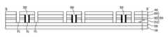
도1은 종래의 직선형의 레이저 스크라이빙을 통해 제작된 박막 광기전력 모듈의 사시도이다.1 is a perspective view of a thin film photovoltaic module manufactured by a conventional straight laser scribing.
기판(100) 상에 순차적으로 하부전극(200), 광전변환층(300) 및 상부전극(400)이 형성되어 있다. 상기 하부전극(200) 사이의 단락을 방지하기 위해 하부전극(200)을 관통하는 하부전극 분리홈(P1)이 형성된다.The
광전변환층(300)을 관통하는 분리홈(P2)이 형성되어 있다. 또한, 상기 광전변환층(300) 및 상기 상부전극(400)을 관통하는 상부 분리홈(P3)이 형성되어 있으며, 이에 의해 단위 셀(UC1, UC2)이 형성된다.And a separation groove P2 through which the
여기서, 상기 광전변환층(300)은 복수의 단위전지층이 적층된 형태일 수 있다. 상기 단위전지층은 광전변환을 수행할 수 있는 기본 단위층이다. 예컨대, 상기 광전변환층(300)은 적층된 두 개의 단위전지층을 포함하거나 세 개의 단위전지층을 포함할 수 있다. 즉, 상기 단위 셀(UC1, UC2) 각각은 복수의 단위전지가 적층된 형태일 수 있다. 상기 광전변환층(300)은 내부반사를 강화하여 빛가둠 효과를 극대화하기 위하여 실리콘 산화물, 실리콘 질화물, 탄화 실리콘 등의 실리콘 합금 중간반사막(intermediate reflective layer)을 포함할 수 있다.Here, the
상기 상부전극(400)과 상기 하부전극(200)을 서로 연결하여 전자의 이동통로로서 기능하는 상기 분리홈(P2)에 의해 서로 인접한 단위 셀(UC1, UC2)들이 직렬 연결된다. 즉, 제1단위셀(UC1)의 하부전극(200)과 제2단위셀(UC2)의 상부전극(400)이 상기 분리홈(P2)을 통해 연결되어 상기 제1단위셀(UC1)과 상기 제2단위셀(UC2)은 직렬 연결된다. 이러한 직렬 연결은 모든 인접 단위 셀들 사이에서 이루어질 수 있다.Unit cells UC1 and UC2 adjacent to each other are connected in series by the separation groove P2 which connects the
도1에 도시된 바와 같이, 상기 하부전극 분리홈(P1), 분리홈(P2) 및 상부 분리홈(P3)은 각각 직선형 라인(210, 310 및 410)을 따르는 레이저 스크라이빙에 의해 형성된다.As shown in FIG. 1, the lower electrode separation groove P1, the separation groove P2, and the upper separation groove P3 are formed by laser scribing along the
이때, 상기 하부전극 분리홈(P1), 분리홈(P2) 및 상부 분리홈(P3)이 연장되어 형성된 부분은 에너지 변환을 수행할 수 없어 무효영역이 된다. 일반적으로, 상기 하부전극 분리홈(P1)과 상기 상부 분리홈(P3) 사이의 간격은 대략 200㎛ 내지 300㎛에 해당하며, 단위 광기전력 셀들이 직렬 연결되는 사이마다 레이저 스크라이빙에 의한 무효영역이 발생하게 된다.At this time, the portion formed by extending the lower electrode separation groove P1, the separation groove P2 and the upper separation groove P3 becomes an invalid region because energy conversion cannot be performed. In general, a distance between the lower electrode separation groove P1 and the upper separation groove P3 corresponds to approximately 200 μm to 300 μm, and is invalid by laser scribing between unit photovoltaic cells connected in series. An area occurs.
모듈에서 에지 아이솔레이션(edge isolation)을 위해서 반도체 및 도체가 제거되고 남은, 광전 변환을 수행하는 영역을 유효 영역이라고 지칭할 때, 상기 유효 영역에 대한 상기 직렬 연결용 레이저 스크라이빙에 의한 무효 영역의 비는 대략 2.5% 내지 5.0%에 해당한다.When the area in which the semiconductor and the conductor are removed for edge isolation in the module and performing photoelectric conversion is referred to as an effective area, the area of the invalid area by the laser scribing for the series connection to the effective area is referred to as an effective area. The ratio corresponds to approximately 2.5% to 5.0%.
따라서, 고효율의 박막 광기전력 모듈을 제작하기 위해서는 레이저 스크라이빙이 수행되는 부분을 최소화하여 무효영역을 줄임으로써 모듈의 광전변환 효율을 높일 수 있는 집적형 박막 광기전력 모듈 및 이의 제조방법이 요구된다. 또한, 높은 에너지 변환 효율을 달성하기 위해 탄뎀형 광기전력 모듈에도 적용될 수 있는 집적 기술에 대한 필요성이 대두되고 있다.Therefore, in order to manufacture a highly efficient thin film photovoltaic module, an integrated thin film photovoltaic module and a method of manufacturing the same may be required to minimize the portion where laser scribing is performed to reduce an invalid region. . In addition, there is a need for an integrated technology that can be applied to tandem photovoltaic modules to achieve high energy conversion efficiency.
본 발명은 상기한 종래 기술의 문제점 및 필요성을 고려하여 고안된 것으로, 광기전력 모듈의 무효 영역을 최소화하여 고효율의 탄뎀형 집적 광기전력 모듈 및 이의 제조 방법을 제공하는 것을 목적으로 한다.The present invention has been devised in consideration of the problems and necessities of the prior art, and aims to provide a high efficiency tandem type integrated photovoltaic module and a method of manufacturing the same by minimizing an invalid area of the photovoltaic module.
본 발명이 이루고자 하는 기술적 과제들은 이상에서 언급한 기술적 과제들로 제한되지 않으며, 언급되지 않은 또 다른 기술적 과제들은 본 발명의 기재로부터 당해 분야에서 통상의 지식을 가진 자에게 명확하게 이해될 수 있을 것이다.The technical objects to be achieved by the present invention are not limited to the above-mentioned technical problems, and other technical subjects which are not mentioned can be clearly understood by those skilled in the art from the description of the present invention .
본 발명의 일 실시예에 따른 탄뎀형 집적 광기전력 모듈은 기판상에 하부전극, 복수의 단위전지층을 포함하는 광전변환층, 및 상부전극이 각각 적층형성된 제1셀 및 제2셀을 포함하며, 상기 제1셀의 하부전극과 상기 제2셀의 하부전극은 하부전극 분리홈에 의해 분리되고, 상기 제2셀의 광전변환층에는 상기 제1셀의 상부전극을 상기 제2셀의 하부전극과 접속시키기 위한 관통홀이 서로 이격되어 복수개 형성되어 있고 상기 관통홀의 측벽에는 고저항층이 형성되어 있다.A tandem integrated photovoltaic module according to an embodiment of the present invention includes a first electrode and a second cell in which a lower electrode, a photoelectric conversion layer including a plurality of unit cell layers, and an upper electrode are stacked on a substrate, respectively. The lower electrode of the first cell and the lower electrode of the second cell are separated by a lower electrode isolation groove, and the upper electrode of the first cell is a lower electrode of the second cell in the photoelectric conversion layer of the second cell. And a plurality of through holes spaced apart from each other, and a high resistance layer is formed on sidewalls of the through holes.
본 발명의 다른 실시예에 따른 탄뎀형 집적 광기전력 모듈의 제조방법은 기판상에 하부전극층을 형성하는 단계, 상기 하부전극층을 제1셀 하부전극층 및 제2셀 하부전극층으로 분리하는 하부전극 분리홈을 형성하는 단계, 상기 제1셀 및 제2셀 하부전극층 상에 복수의 단위전지층을 포함하는 광전변환층을 형성하는 단계, 상기 제2셀 하부전극층상의 광전변환층을 관통하는 서로 이격된 복수의 관통홀을 형성하는 단계, 상기 관통홀의 측벽에 고저항층을 형성하는 단계, 상기 관통홀 내부 및 상기 광전변환층 상에 상부전극층을 형성하는 단계; 및 상기 상부전극층 및 상기 광전변환층을 분리하는 상부 분리홈을 그 일부가 상기 하부전극 분리홈 위를 지나도록 형성하는 단계를 포함한다.In another embodiment of the present invention, a method of manufacturing a tandem integrated photovoltaic module includes forming a lower electrode layer on a substrate, and separating the lower electrode layer into a first cell lower electrode layer and a second cell lower electrode layer. Forming a photovoltaic layer including a plurality of unit cell layers on the first cell and the second cell lower electrode layer, and spaced apart from each other through the photoelectric conversion layer on the second cell lower electrode layer Forming a through hole of the upper hole layer, forming a high resistance layer on the sidewall of the through hole, and forming an upper electrode layer in the through hole and on the photoelectric conversion layer; And forming an upper separation groove separating the upper electrode layer and the photoelectric conversion layer so that a portion thereof passes over the lower electrode separation groove.
본 발명에 따르면, 포인트 컨택을 통해 광기전력 모듈 내의 단위 셀들이 직렬 연결되도록 함으로써 광기전력 모듈 내의 무효 영역을 줄여 모듈의 효율을 높일 수 있다. 또한, 본 발명에 따르면, 탄뎀형 관기전력 모듈의 누설 전류를 줄여 그 효율을 높일 수 있다. 또한, 본 발명에 따르면 빛의 내부반사를 강화하여 탄뎀형 광기전력 모듈의 효율을 높일 수 있다. 또한, 본 발명에 따르면 탄뎀형 집적 광기전력 모듈 및 이의 제조방법을 제공할 수 있다.According to the present invention, the unit cells in the photovoltaic module are connected in series through a point contact, thereby reducing the invalid area in the photovoltaic module, thereby increasing the efficiency of the module. In addition, according to the present invention, it is possible to reduce the leakage current of the tandem-type ER module to increase its efficiency. In addition, according to the present invention can enhance the internal reflection of light to increase the efficiency of the tandem photovoltaic module. In addition, the present invention can provide a tandem type integrated photovoltaic module and a method of manufacturing the same.
도 1은 종래의 직선형의 레이저 스크라이빙을 통해 제작된 박막 광기전력 모듈의 사시도이다.
도 2는 본 발명의 일 실시예에 따라 포인트 컨택을 통해 직렬 연결되는 광기전력 셀들을 포함하는 광기전력 모듈의 사시도를 나타낸다.
도3a 및 도3b는 도2의 a-a' 및 b-b'에 따른 단면도이다.
도4a 내지 도4g는 본 발명의 일 실시예에 따른 탄뎀형 집적 광기전력 모듈의 제조과정을 나타낸다.
도5a 및 도5b는 호모지나이저를 통과하기 전 및 통과한 후의 레이저빔의 강도분포 및 이에 따른 패턴면을 나타낸다.
도5c는 호모지나이저를 통과한 레이저빔에 의해 형성된 패턴의 단면을 나타낸다.
도6은 도2의 점선 사각형 부분(A)의 확대도이다.
도7a 내지 도7c는 본 발명의 실시예에 따른 관통홀을 둘러싸는 제2라인의 형상을 예시한다.1 is a perspective view of a thin film photovoltaic module manufactured by a conventional straight laser scribing.
2 illustrates a perspective view of a photovoltaic module including photovoltaic cells connected in series via point contacts in accordance with one embodiment of the present invention.
3A and 3B are cross-sectional views taken along aa 'and b-b' of FIG.
4A to 4G illustrate a manufacturing process of a tandem integrated photovoltaic module according to an embodiment of the present invention.
5A and 5B show the intensity distribution of the laser beam before and after passing through the homogenizer and the patterned surface accordingly.
Fig. 5C shows a cross section of the pattern formed by the laser beam passing through the homogenizer.
FIG. 6 is an enlarged view of the dotted rectangle portion A of FIG. 2.
7A-7C illustrate the shape of a second line surrounding a through hole in accordance with an embodiment of the present invention.
이하, 본 발명의 바람직한 실시예의 상세한 설명이 첨부된 도면들을 참조하여 설명된다. 그러나, 본 발명의 실시 형태는 여러 가지의 다른 형태로 변형될 수 있으며, 본 발명의 범위가 이하 설명하는 실시형태로만 한정되는 것은 아니다. 도면에서의 요소들의 형상 및 크기 등은 보다 명확한 설명을 위해 과장될 수 있으며, 도면들 중 인용부호들 및 동일한 구성요소들에 대해서는 비록 다른 도면상에 표시되더라도 가능한 한 동일한 인용부호들로 표시됨을 유의해야 한다. 참고로 본 발명을 설명함에 있어서 관련된 공지 기능 혹은 구성에 대한 구체적인 설명이 본 발명의 요지를 불필요하게 흐릴 수 있다고 판단되는 경우 그 상세한 설명을 생략한다.DETAILED DESCRIPTION OF THE PREFERRED EMBODIMENTS Hereinafter, a detailed description of preferred embodiments of the present invention will be given with reference to the accompanying drawings. However, the embodiments of the present invention may be modified into various other forms, and the scope of the present invention is not limited to the embodiments described below. The shape and the size of the elements in the drawings may be exaggerated for clarity of explanation and the same reference numerals are used for the same elements and the same elements are denoted by the same quote symbols as possible even if they are displayed on different drawings Should be. In the following description, well-known functions or constructions are not described in detail to avoid unnecessarily obscuring the subject matter of the present invention.
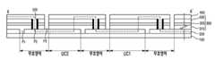
도2는 본 발명의 일 실시예에 따라 포인트 컨택(point contact)을 통해 직렬 연결되는 광기전력 셀들을 포함하는 광기전력 모듈의 사시도를 나타낸다. 도1 및 이하의 도면에서는 하부전극 분리홈(P1), 관통홀(P2) 및 상부 분리홈(P3)의 형상이 광기전력 모듈의 상부 표면에 표시되지만 이는 설명의 편의를 위한 것으로서, 상기 형상들은 상부 표면에서 관찰되지 않을 수 있다.FIG. 2 illustrates a perspective view of a photovoltaic module including photovoltaic cells connected in series via point contact in accordance with one embodiment of the present invention. In FIG. 1 and the following drawings, the shape of the lower electrode separation groove P1, the through hole P2, and the upper separation groove P3 is shown on the upper surface of the photovoltaic module, but for convenience of description, the shapes are May not be observed at the top surface.
본 발명의 일 실시예에 따른 광기전력 모듈은 기판(100), 하부전극(200), 광전변환층(300) 및 상부전극(400)을 포함한다. 본 발명의 다른 실시예에 따른 광기전력 모듈은 상기 광전변환층(300)과 상기 상부전극(400) 사이에 투명 전도막을 더 포함할 수 있다.The photovoltaic module according to an embodiment of the present invention includes a
여기서, 상기 광전변환층(300)은 복수의 단위전지층(310, 330)을 포함할 수 있다. 예컨대, 상기 광전변환층(300)은 적층된 두 개의 단위전지층을 포함하거나 세 개의 단위전지층을 포함할 수 있다. 상기 적층된 각각의 단위전지층은 광전변환을 수행하는 기본 단위층이다. 이때, 상기 복수의 단위전지층(310, 330) 사이에는 터널접합이 이루어진다.The
예컨대, 광전변환층(300)은 제1단위전지층(310)과 제2단위전지층(330)을 포함할 수 있다. 상기 제1단위전지층(310)과 상기 제2단위전지층(330) 각각은 p형 반도체층 및 n형 반도체층을 포함한다. 이때, 제1단위전지층(310)의 p형 반도체층과 제2단위전지층(330)의 n형 반도체층이 서로 인접하여 pn 터널접합을 형성하거나, 제1단위전지층(310)의 n형 반도체층과 제2단위전지층(330)의 p형 반도체층이 서로 인접하여 pn 터널접합을 형성할 수 있다. 이러한 pn 터널접합은, 광전변환층(300)이 복수의 단위전지층을 포함하는 경우 복수의 단위전지층 사이마다 발생한다. 이와 같이 pn 터널접합이 이루어질 때 pn 터널접합부는 저항이 매우 낮아져 전도도가 높아진다.For example, the
상기 적층된 단위전지층 사이에는 내부 반사를 강화하여 빛가둠 효과를 극대화하기 위하여 중간 반사막이 삽입될 수 있다. 예컨대, 상기 광전변환층(300)이 두 개의 단위전지층을 포함하는 경우, 상기 두 개의 단위전지층 사이에 중간 반사막이 삽입될 수 있다. 상기 중간 반사막은 실리콘 산화물, 실리콘 질화물, 탄화 실리콘 등의 실리콘 합금을 포함할 수 있다. 또한, 상기 중간 반사막은 투광성 물질을 포함할 수 있으며, 상기 투광성 물질로는 ZnO, SiO 또는 SnO2 중 적어도 하나를 포함할 수 있다.An intermediate reflective film may be inserted between the stacked unit cell layers to maximize the light confinement effect by enhancing internal reflection. For example, when the
상기 광전변환층(300)이 복수의 단위전지층을 포함하는 경우, 서로 직렬 연결된 광기전력 셀(UC1, UC2) 각각은 복수의 단위전지(310, 330)가 적층된 형태일 수 있다. 상기 광기전력 셀(UC1, UC2)의 개방전압은 상기 적층된 단위전지(310, 330)들의 개방전압의 합이고, 상기 단위 셀(UC1, UC2)의 단락전류는 상기 적층된 단위전지들의 단락전류 중 최소의 단락전류 값을 갖는다.도2에 도시된 바와 같이, 하부전극 분리홈(P1)은 하부전극(200) 사이의 단락을 방지하기 위해 하부전극(200)을 관통하여 형성된다. 상기 하부전극 분리홈(P1)은 예컨대 직선형의 제1라인(220)을 따라 형성될 수 있다.When the
광전변환층(300)을 관통하는 관통홀(P2)이, 직선 형태가 아닌 소정의 너비를 갖는 포인트 형태로서 이격되어 상기 하부전극 분리홈(P1)의 일 측에 복수 개 형성된다. 본 발명의 다른 실시예에 따라 상기 관통홀(P2)은 상기 광전변환층(300)과 상기 투명 전도막을 관통하도록 형성될 수 있다. 인접한 단위 셀들(UC1 및 UC2)은 상기 관통홀(P2)을 통해 직렬 연결된다. 즉, 제1단위셀(UC1)의 상부전극(400)과 제2단위셀(UC2)의 하부전극(200)이 포인트 형태인 상기 관통홀(P2)을 통해 연결되어 상기 제1단위셀(UC1)과 상기 제2단위셀(UC2)이 직렬 연결될 수 있다. 본 명세서에서는 상기 관통홀(P2)이 포인트 형태인 것이 예시되나, 이는 단지 예시일 뿐이며, 상기 복수개의 관통홀(P2)이 이격되어 형성되어 있다면 상기 관통홀(P2)은 일 방향으로 연장된 분절된 직선형상일 수 있다.A plurality of through holes P2 penetrating the
도2의 광기전력 모듈의 a-a' 선에 따른 단면도가 도3a에 도시된다. 도3a에 도시된 바와 같이, 상기 관통홀(P2)이 형성된 부분은 종래 기술에 따른 도1의 광기전력 모듈의 단면과 동일함을 알 수 있다. 비록 관통홀(P2)이 직선형 라인을 따라 형성되지 않더라도, 각 단위 셀들(UC1, UC2)은 상기 이격되어 형성된 관통홀(P2)이 형성된 부분을 통해서 여전히 직렬 연결될 수 있다.A cross-sectional view along line a-a 'of the photovoltaic module of FIG. 2 is shown in FIG. 3A. As shown in Figure 3a, it can be seen that the portion in which the through hole P2 is formed is the same as the cross section of the photovoltaic module of Figure 1 according to the prior art. Although the through holes P2 are not formed along the straight line, the unit cells UC1 and UC2 may still be connected in series through portions of the through holes P2 spaced apart from each other.
본 발명의 실시예에 따르면 복수의 단위전지층 사이에 전도도가 높은 pn 터널접합이 이루어지더라도 관통홀(P2)에 충진된 상부전극(400)과 pn 터널접합부가 접촉함으로써 발생할 수 있는 누설 전류의 발생이 방지될 수 있다.또한, 중간반사막(320)이 전도성 물질일지라도 상기 관통홀(P2)에 충진된 상부전극(400)과 중간 반사막(320)이 접촉함으로써 발생할 수 있는 누설 전류의 발생이 방지될 수 있다. 이는 도3a에 도시된 바와 같이, 상기 관통홀(P2)의 측벽에 고저항층(500)을 형성함으로써 달성될 수 있다. 따라서, 관통홀(P2) 내에 충진된 상부전극(400) 물질과 pn 터널접합부 및/또는 중간 반사막(320)이 전기적으로 절연 상태에 있어 누설 전류의 발생을 방지할 수 있다. 결과적으로 누설 전류로 인해 광기전력 모듈의 필팩터(fill factor)가 감소되는 것이 방지될 수 있다. 도3a에는 상기 고저항층(500)이 상기 관통홀(P2)의 측벽 전체에 형성된 것이 도시되지만, 상기 고저항층(500)은 pn 터널접합부 및/또는 도전성 물질로 형성된 중간반사막이 노출된 측벽에만 형성될 수 있다.According to an exemplary embodiment of the present invention, even when a high conductivity pn tunnel junction is formed between a plurality of unit cell layers, leakage current that may be generated by contacting the
상부 분리홈(P3)은 상기 광전변환층(300)과 상기 상부전극(400)을 관통하여 형성되며, 이에 따라 단위 셀(UC1, UC2)들이 형성된다. 상기 상부 분리홈(P3)은 포인트 형태의 관통홀(P2)을 소정의 형상으로 둘러싸는 것을 제외하고는 상기 하부전극 분리홈(P1) 상에 형성된다. 예컨대, 상기 상부 분리홈(P3)은 제2라인(420)을 따라 형성될 수 있다.The upper separation groove P3 is formed through the
이때, 상기 하부전극 분리홈(P3)의 길이에 대한 상기 상부 분리홈과 상기 하부전극 분리홈이 중첩되는 길이의 비는 0.70 이상 0.96 이하일 수 있다. 상기 비율이 0.70보다 작은 경우에는 무효영역이 증가하므로 충분한 전류 상승의 효과를 얻을 수 없고 제조시간이 증가할 수 있다. 상기 비율이 0.96보다 큰 경우에는 전자의 이동 경로가 증가하여 저항 및 줄열이 커져 광기전력 모듈의 필팩터(fill factor)가 감소할 수 있다.In this case, the ratio of the length of the upper separation groove and the lower electrode separation groove to the length of the lower electrode separation groove P3 may be 0.70 or more and 0.96 or less. If the ratio is less than 0.70, the invalid region increases, so that the effect of sufficient current rise cannot be obtained, and the manufacturing time can increase. When the ratio is greater than 0.96, the path of electrons increases to increase resistance and Joule heat, thereby reducing the fill factor of the photovoltaic module.
본 발명의 이해를 위해 도2의 광기전력 모듈의 b-b' 선에 따른 단면도가 도3b에 도시된다. 도2에 도시된 바와 같이, 상기 상부 분리홈(P3)이 상기 하부전극 분리홈(P1) 상에 형성되는 부분에서는 상기 상부 분리홈(P3)은 기판(100)의 상면까지 연장된다. 반면에, 도3b에 도시된 바와 같이, 상기 상부 분리홈(P3)이 상기 하부전극 분리홈(P1) 위를 지나지 않는 부분에서는 상기 상부 분리홈(P3)은 상기 하부전극(200)의 상면까지만 연장된다. 이는, 상기 상부 분리홈(P3)이 광전변환층(300)과 상부전극(400)을 관통하여 형성되지만, 상기 하부전극 분리홈(P1)이 형성된 부분에는 이미 하부전극(200)이 상기 하부전극 분리홈(P1)에 의해 제거되었기 때문이다.A cross-sectional view along line b-b 'of the photovoltaic module of FIG. 2 is shown in FIG. 3b for the understanding of the present invention. As shown in FIG. 2, in the portion in which the upper separation groove P3 is formed on the lower electrode separation groove P1, the upper separation groove P3 extends to the upper surface of the
상기와 같이, 하부전극 분리홈(P1)이 형성되는 제1라인(220)과 상부 분리홈(P3)이 형성되는 제2라인(420)이 특정 영역을 제외하고는 중첩되기 때문에, 본 발명의 실시예에 따른 광기전력 모듈의 무효 영역이 감소된다. 또한, 광기전력 모듈 내의 단위 셀들을 직렬 연결하기 위한 관통홀(P2)이 포인트 컨택 형태로 소정의 간격을 두고 형성되므로 광기전력 모듈의 무효 영역이 감소될 수 있다. 따라서, 동일 면적 대비 유효 영역의 면적이 증가하기 때문에 상대적 전류 값의 향상을 볼 수 있다.As described above, since the
이하에서는, 본 발명의 일 실시예에 따라 포인트 컨택을 통해 서로 직렬 연결되는 광기전력 셀들을 포함하는 광기전력 모듈의 제조 과정을 도4a 내지 도4g를 참조하여 상세히 설명한다. 도4a 내지 도4g는 3개의 단위 셀들을 도시하지만 본원 발명의 광기전력 모듈은 더 많은 수의 단위 셀들을 포함할 수 있다.Hereinafter, a manufacturing process of a photovoltaic module including photovoltaic cells connected in series to each other through a point contact according to an embodiment of the present invention will be described in detail with reference to FIGS. 4A to 4G. 4A-4G show three unit cells but the photovoltaic module of the present invention may include a greater number of unit cells.
도4a에 도시된 바와 같이, 기판(100)이 준비된다. 상기 기판(100)은 절연성 투명기판일 수 있다. 본 발명의 실시예에 따른 광기전력 모듈이 상부전극(400) 측에서 조사되는 빛에 의해 광전변환을 수행하는 경우 상기 기판(100)은 불투명 절연성 기판일 수 있다. 또한, 상기 기판(100)은 유연한 기판일 수 있다.As shown in Fig. 4A, a
도4b에 도시된 바와 같이, 상기 기판(100) 상에 하부전극(200)이 형성된다. 상기 하부전극(200)은 산화주석(SnO2), 산화아연(ZnO) 또는 산화인듐주석(ITO) 등을 포함하는 투명전극일 수 있다. 본 발명의 실시예에 따른 광기전력 모듈이 상부전극(400) 측에서 조사되는 빛에 의해 광전변환을 수행하는 경우 상기 하부전극(200)은 불투명 전극일 수 있다.As shown in FIG. 4B, a
도4c에 도시된 바와 같이, 대기 중에서 레이저가 하부전극(200) 측이나 기판(100)측으로 조사되어 하부전극(200)이 스크라이브(scribe)된다. 이에 의하여 하부전극(200)을 관통하여 분리하는 하부전극 분리홈(P1)이 예컨대 직선형의 제1라인(220)을 따라 형성된다. 즉, 하부전극 분리홈(P1)에 의해 하부전극(200)이 서로 분리되므로 인접한 하부전극들(200) 사이의 단락이 방지된다.As shown in FIG. 4C, the laser is irradiated to the
도4d에 도시된 바와 같이, 상기 하부전극(200)상에 광전변환층(300)이 형성된다. 이때, 상기 광전변환층(300)은 하부전극 분리홈(P1) 상에도 형성될 수 있다. 예컨대, 상기 하부전극(200) 상에 복수의 단위전지층(310, 330)을 포함하는 광전변환층(300)이 형성될 수 있다. 이하에서는, 2개의 단위전지층을 포함하는 광전변환층(300)에 대해서 설명하나, 본 발명의 실시예에 따라 3개 이상의 단위전지층이 광전변환층(300)에 포함될 수 있다. 또한, 본 발명의 실시예에 따라 상기 단위전지층들 사이에는 중간반사막(320)이 포함될 수 있다.As shown in FIG. 4D, a
상기 제1 및 제2단위전지층(310 및 330)은 입사된 빛 에너지를 전기 에너지로 변환하는 임의의 물질을 포함할 수 있다. 예를 들어, 상기 제1 및 제2단위전지층(310, 330)은 비정질 실리콘 계열, 화합물 계열, 유기물 계열 및 염료 감응형 태양전지와 같은 박막형 광기전력 모듈을 형성할 수 있는 광전변환 물질을 포함할 수 있다.The first and second unit cell layers 310 and 330 may include any material that converts incident light energy into electrical energy. For example, the first and second unit cell layers 310 and 330 may include photoelectric conversion materials capable of forming thin film photovoltaic modules such as amorphous silicon based, compound based, organic based, and dye-sensitized solar cells. can do.
상기 중간반사막(320)은 상기 제1단위전지층과 제2 단위전지층 중에서 빛이 먼저 입사되는 단위전지층을 통과한 빛의 일부는 상기 빛이 먼저 입사되는 단위전지층으로 반사하고 일부는 나머지 단위전지층으로 통과시킨다. 이에 따라 빛이 먼저 입사되는 단위전지층에 의하여 흡수되는 빛의 양이 증가하여 상기 단위전지층에서 발생하는 전류가 증대될 수 있다.The
이때, 상기 제1 및 제2 단위전지층 중에 빛이 입사되는 측에서 가까운 단위전지층의 광학적 밴드갭은 나머지 단위전지층의 광학적 밴드갭보다 클 수 있다. 예컨대, 빛이 기판(100)을 통해 입사되는 경우 제1 단위전지층의 광학적 밴드갭이 제2 단위전지층의 광학적 밴드갭보다 크다. 이는, 에너지 밀도가 높은 단파장의 빛은 투과 거리가 짧으며, 광학적 밴드갭이 큰 물질일수록 단파장의 빛을 잘 흡수하기 때문이다.In this case, the optical bandgap of the unit cell layer close to the light incident side of the first and second unit cell layer may be larger than the optical bandgap of the remaining unit cell layer. For example, when light is incident through the
본 명세서에서 지칭되는 광전변환층(300)은 실시예에 따라 단위전지층들 및 상기 단위전지층들 사이에 삽입된 중간반사막을 포함할 수 있다. 상기 광전변환층(300)의 단위전지층들은 일반적으로 진공 상태에서 형성되고 하부전극 분리홈(P1), 관통홀(P2) 및 상부 분리홈(P3)을 형성하는 레이저 패터닝은 대기 중에서 이루어진다. 따라서, 도4e와 관련하여 이하에서 설명되는 관통홀(P2)을 형성하기 위한 레이저 스크라이빙을 수행하기 위해 상기 광전변환층(300)은 대기 중에 노출되어야 한다. 이와 같이 대기 중에 상기 광전변환층(300)이 노출되는 동안에 상기 광전변환층(300)에는 산화가 이루어져 광전변환층(300)이 변질될 수 있다. 결과적으로 제조되는 광기전력 모듈의 효율이 저하될 수 있다.The
따라서, 본 발명의 다른 실시예에 따른 광기전력 모듈의 제조시에, 상기 광전변환층(300)을 진공 중에서 형성하고 대기 중에서 관통홀(P2)을 형성하기 전에, 상기 광전변환층 상에 투명 전도막을 진공 중에서 형성하는 단계를 더 포함할 수 있다. 이와 같이, 상기 광전변환층(300) 상에 상기 투명 전도막을 진공 중에서 형성함으로써 상기 광전변환층(300)이 대기 중에 노출되어 변질되는 것을 방지할 수 있다. 예컨대, 상기 광전변환층(300)은 상기 투명 전도막이 그 위에 형성되어 있기 때문에 대기중에서 레이저 스크라이빙을 수행하는 동안에도 그의 산화가 방지될 수 있다.Therefore, in the manufacturing of the photovoltaic module according to another embodiment of the present invention, before forming the
상기 투명 전도막은 전술한 바와 같이 상기 광전변환층(300)을 보호하는 역할뿐만 아니라 상기 광전변환층(300)과 상부전극(400) 사이에서 빛 가둠 현상(light trapping effect)을 극대화할 수 있다. 즉, 상기 투명 전도막은 상기 광전변환층(300)에서 광전변환에 이용되지 못하는 빛을 반사하여 상기 광전변환층(300)에서 재사용되게 함으로써 빛의 이용효율을 높일 수 있다. 상기 투명 전도막은 예컨대 산화아연(ZnO) 또는 인듐 주석 산화물(ITO)같은 물질을 포함할 수 있다.As described above, the transparent conductive film may maximize the light trapping effect between the
이하에서, 관통홀(P2)은 비록 광전변환층(300)만을 관통하도록 기재하고 있지만, 실시예에 따라 상기 관통홀(P2)은 광전변환층(300)과 상기 광전변환층(300) 상에 형성된 투명 전도막을 관통하여 형성될 수 있다. 또한, 상부 분리홈(P3)도 광전변환층(300)과 상부전극(400)을 관통하여 형성되도록 기재하지만 실시예에 따라 상부 분리홈(P3)은 광전변환층(300), 투명 전도막 및 상부전극(400)을 관통하여 형성될 수 있다.Hereinafter, although the through hole P2 is described to penetrate only the
도4e에 도시된 바와 같이, 대기중에서 레이저가 기판(100) 측이나 광전변환층(300) 측으로 조사되어 광전변환층(300)이 스크라이브된다. 이에 의하여 광전변환층(300)을 관통하는 관통홀(P2)이 복수 개 형성된다. 상기 관통홀(P2)은 종래 기술과 달리 직선형 라인을 따라 형성되지 않는다. 상기 관통홀(P2)은 소정의 너비를 갖는 포인트 형태로서 서로 이격되어 상기 하부전극 분리홈(P1)의 일 측에 복수 개 형성될 수 있다. 이렇게 형성된 관통홀(P2)을 통해 광기전력 모듈 내의 단위 셀들 사이의 직렬 연결이 이루어진다.As shown in FIG. 4E, the laser is irradiated to the
그 다음, 도3a 및 도3b에 도시된 바와 같이, 상기 관통홀(P2)의 내부 측벽에 고저항층(500)이 형성된다. 상기 고저항층(500)은 상기 광전변환층(300)의 pn 터널접합부가 노출된 부분에만 형성될 수 있다. 또한 상기 고저항층(500)은 상기 pn 터널접합부 및 중간반사막(320)이 노출된 부분에만 형성될 수도 있다. 상기 고저항층(500)은 상기 광전변환층(300) 내에 존재하는 도전성 층이 상기 관통홀(P2)에 충진되는 상부전극(400) 물질과 접촉함으로써 발생할 수 있는 전류의 누설을 방지하기 위한 것이다.3A and 3B, a
예컨대, 상기 제1단위전지층(310)과 상기 제2단위전지층(330)은 각각 아래 순서대로 적층된 p형 반도체층 및 n형 반도체층을 포함한다. 이때, 제1단위전지층의 n형 반도체층과 제2단위전지층의 p형 반도체층 사이에 pn 터널접합이 일어날 수 있다. 실시예에 따라 상기 제1 및 제2단위전지층(310, 330)은 각각 아래 순서대로 적층된 n형 반도체층 및 p형 반도체층을 포함할 수 있다. 이때, 제1단위전지층의 p형 반도체층과 제2단위전지층(330)의 n형 반도체층 사이에 pn 터널접합이 일어날 수 있다.For example, the first
이때, 상기 고저항층(500)은 pn 터널접합부가 관통홀(P2)에 의해 노출된 측벽에 형성될 수 있다. 제1단위전지층(310)과 제2단위전지층(330) 사이에 중간반사막(320)을 포함하는 경우, 상기 고저항층(500)은 상기 중간반사막(320) 및 상기 pn 터널접합부가 상기 관통홀(P2)에 의해 노출된 측벽에 형성될 수 있다.In this case, the
이는 전도도가 높은 pn 터널접합부 및/또는 중간반사막(320)이 관통홀(P2)을 통해 상부전극(400)과 접촉하는 경우에 누설 전류가 발생할 가능성이 있기 때문이다. 따라서, 상기 고저항층(500)이 상기 중간반사막(320) 및/또는 pn 터널접합부가 노출된 측벽에 형성되도록 함으로써 상기와 같은 누설 전류의 발생을 방지할 수 있다.This is because leakage current may occur when the high conductivity pn tunnel junction and / or the
상기 고저항층(500)은 플라즈마 처리를 통해 관통홀(P2)의 측벽에 형성될 수 있다. 고저항 원소로는 산소, 질소 및 탄소 등이 포함된다. 이때, 적어도 하나 이상의 고저항 원소를 포함하는 가스 분위기에서 플라즈마 처리를 함으로써 고저항층(500)이 관통홀(P2)의 측벽에 형성될 수 있다.The
또는, 레이저(laser)나 전자선 이온(ion) 조사와 같은 물리적 방법, 또는 화학약품 등을 이용한 화학적 방법으로 관통홀(P2) 측벽을 산화시킴으로써 고저항층(500)이 형성될 수 있다.Alternatively, the
이에 따라, 고저항층(500)이 관통홀(P2)의 측벽에 형성됨으로써 pn 터널접합부 및/또는 중간반사막(320)이 상부전극(400) 물질과 접촉하는 것이 방지되어 누설 전류가 발생하는 것을 방지할 수 있다. 또한, 탄소, 산소 또는 질소와 같은 고저항 원소는 굴절률을 낮추는데 기여하므로, 상기와 같이 관통홀(P2)의 측벽에 고저항층(500)을 형성함으로써 내부반사를 강화할 수 있다. 이에 따라 광기전력 모듈의 빛 이용률을 향상시켜 전류 향상에 기여할 수 있다.Accordingly, since the
도4f에 도시된 바와 같이, 상기 광전변환층(300) 및 상기 관통홀(P2)을 덮는 상부전극(400)이 형성된다. 상기 상부전극(400)은 빛을 반사하는 특성이 좋고, 전극으로서 기능하는 전도성 물질을 포함할 수 있다. 예컨대, 상기 상부전극(400)을 형성하는 전도성 물질은 알루미늄(Al), 은(Ag), 금(Au), 구리(cu), 아연(Zn), 니켈(Ni), 백금(Pt), 팔라듐(Pd) 또는 크롬(Cr) 등을 포함할 수 있다. 또한, 본 발명의 실시예에 따른 광기전력 모듈이 상부전극(400) 측에서 조사되는 빛에 의해 광전변환을 수행하는 경우 상기 상부전극(400)은 투명 전도성 물질로 형성될 수 있다. 이 경우 상기 하부전극(200)은 빛을 반사하는 특성이 좋고 전극으로서 기능하기 위한 전도성 물질을 포함할 수 있다.As shown in FIG. 4F, an
도4g에 도시된 바와 같이, 대기중에서 레이저가 조사되어 광전변환층(300) 및 상부전극(400)이 스크라이브된다. 이에 따라, 상기 광전변환층(300) 및 상기 상부전극(400)을 관통하는 상부 분리홈(P3)이 제2라인(420)을 따라 형성될 수 있다. 상기 제2라인(420)은 포인트 형태의 상기 관통홀(P2)을 둘러싸는 것을 제외하고는 상기 제1라인(220)과 동일한 경로를 따른다. 즉, 상기 상부 분리홈(P3)은 상기 관통홀(P2)을 둘러싸는 부분을 제외하고는 상기 하부전극 분리홈(P1) 위를 지나도록 형성된다. 상기 상부 분리홈(P3)을 통해 단위 셀들(UC1, UC2)이 정의된다.As shown in FIG. 4G, the laser is irradiated in the air to scribe the
본 발명의 다른 실시예에 따르면, 상기 상부전극을 진공에서 형성하고 대기 중에서 레이저 스크라이빙에 의해 상부 분리홈(P3)을 형성하는 과정은, 패턴이 형성된 상부전극을 비진공 상태에서 인쇄하는 방식으로 대체될 수 있다. 예컨대, 제2라인(420)의 형상으로 패턴화된 상부전극은 비진공 상태에서 레이저 프린팅, 잉크젯 프린팅, 및 스크린 프린팅 등과 같은 프린팅 방법으로 상기 광전변환층(300) 상에 형성될 수 있다. 이와 같이 패턴화된 상부전극을 진공 상태가 아닌 대기 중에서 형성함으로써 제조 단가가 절감될 수 있다.According to another embodiment of the present invention, the process of forming the upper electrode in the vacuum and the upper separation groove (P3) by laser scribing in the atmosphere, the method of printing the patterned upper electrode in a non-vacuum state Can be replaced with For example, the upper electrode patterned in the shape of the
전술한 본 발명의 일 실시예에 따른 광기전력 모듈의 제조 과정에서는 하부전극 분리홈(P1)은 제1라인(220)을 따라 형성되고 상부 분리홈(P3)은 제2라인(420)을 따라 형성된 것을 예시하지만, 하부전극 분리홈(P1)이 제2라인(420)을 따라 형성되고 상부 분리홈(P3)이 제1라인(220)을 따라 형성되는 것도 가능하다.The lower electrode separation groove P1 is formed along the
또한, 도2 및 전술한 본 발명의 일 실시예에 따른 광기전력 모듈의 제조 과정에서는 하부전극 분리홈(P1)의 폭을 상부 분리홈(P3)의 폭보다 넓게 도시하고 있지만, 이는 단지 예시일 뿐이며 하부전극 분리홈(P1)의 폭은 상부 분리홈(P3)의 폭과 동일하거나 더 작을 수 있다.In addition, in the manufacturing process of the photovoltaic module according to the embodiment of FIG. The width of the lower electrode separation groove P1 may be the same as or smaller than the width of the upper separation groove P3.
전술한 본 발명의 실시예에 따른 광기전력 모듈의 제조 과정에서, 하부전극 분리홈(P1), 관통홀(P2) 및 상부 분리홈(P3) 중 적어도 하나는 레이저 스크라이빙에 의해 형성될 수 있다. 이러한 레이저 스크라이빙을 수행하는 레이저 가공기(미도시)는 레이저 발진기에서 발진된 레이저 빔의 강도 분포가 조사되는 영역에서 균일하게 되도록 호모지나이저(homogenizer)를 구비할 수 있다. 이러한 호모지나이저는 구면렌즈의 조합이나 전반사 특성을 이용하는 광 섬유 케이블 등으로 이루어질 수 있다.In the manufacturing process of the photovoltaic module according to the embodiment of the present invention described above, at least one of the lower electrode separation groove (P1), the through hole (P2) and the upper separation groove (P3) may be formed by laser scribing. have. A laser processing machine (not shown) that performs such laser scribing may include a homogenizer so that the intensity distribution of the laser beam oscillated by the laser oscillator is uniform in the area irradiated. The homogenizer may be made of an optical fiber cable using a combination of spherical lenses or total reflection characteristics.
도5a 및 도5b를 참조하면, 레이저 발진기에서 발진된 가우시안 강도 분포를 갖는 레이저 빔이 호모지나이저를 통과하게 되면, 균일한 강도 분포를 갖는 레이저 빔이 된다. 또한, 도5a 및 도5b를 참조하면, 가우시안 강도 분포(도5a)를 갖는 레이저 빔을 이용한 패턴면은 호모지나이저를 통과하여 균일한 강도 분포(도5b)를 갖는 레이저 빔을 이용한 패턴면에 비해 매우 불규칙적임을 알 수 있다.5A and 5B, when a laser beam having a Gaussian intensity distribution oscillated in a laser oscillator passes through a homogenizer, it becomes a laser beam having a uniform intensity distribution. 5A and 5B, a pattern surface using a laser beam having a Gaussian intensity distribution (FIG. 5A) passes through a homogenizer to a pattern surface using a laser beam having a uniform intensity distribution (FIG. 5B). It can be seen that it is very irregular.
즉, 레이저 빔의 강도 분포가 균일해지면, 레이저 빔이 조사되어 형성되는 분리홈들의 패턴면은 실질적으로 균일하게 형성된다. 이에 의해, 하부전극 분리홈, 관통홀 및/또는 상부 분리홈(P1, P2, P3)의 측벽 등에서 버(burr) 발생을 최소화 할 수 있어, 효율이 개선된 집적형 박막 광기전력 모듈을 제조할 수 있다. 또한, 이와 같이 호모지나이저를 통과한 레이저 빔을 사용함으로써 원하는 절연 특성을 구현하기 위해 레이저 파워가 가해져서 주변의 광전변환층 및 전극의 특성이 변하는 것을 방지할 수 있다.That is, when the intensity distribution of the laser beam is uniform, the pattern surface of the separation grooves formed by irradiating the laser beam is formed substantially uniformly. As a result, burrs may be minimized in the sidewalls of the lower electrode separation groove, the through hole, and / or the sidewalls of the upper separation grooves P1, P2, and P3, thereby manufacturing an integrated thin film photovoltaic module having improved efficiency. Can be. In addition, by using the laser beam passed through the homogenizer as described above, laser power is applied to implement desired insulation properties, thereby preventing the characteristics of the surrounding photoelectric conversion layer and the electrode from being changed.
또한, 상기 레이저 가공기는 상기 호모지나이저를 통과한 레이저 빔이 선택적으로 투과될 수 있도록 소정의 패턴이 형성된 마스크를 포함할 수 있다. 이에 따라 원하는 정도의 균일한 강도 분포를 나타내는 레이저 빔의 영역만을 분리홈 또는 관통홀을 형성하는데 사용할 수 있다.In addition, the laser processing machine may include a mask having a predetermined pattern formed to selectively transmit the laser beam passing through the homogenizer. Accordingly, only the region of the laser beam showing a uniform intensity distribution of a desired degree can be used to form the separation groove or the through hole.
도5c에는 발명의 실시예에 따라 형성된 분리홈 또는 관통홀 패턴의 단면이 도시된다. 이때, 패턴의 폭(W)에 대한 패턴의 바닥면의 단차(h)의 비는 5% 이상 10% 이하인 것이 바람직하다. 상기 패턴의 폭(W)에 대한 상기 단차(h)의 비가 10%보다 큰 경우 패턴의 가장 자리가 충분히 제거되지 않아 누설(leak) 전류가 발생할 수 있다. 상기 패턴의 폭(W)에 대한 상기 단차(h)의 비를 5% 보다 작게 구현하기 위해서는 과도한 레이저 파워가 가해져 주변의 광전변환층 및 전극의 특성이 변할 수 있다.5C shows a cross section of a separation groove or through hole pattern formed in accordance with an embodiment of the invention. At this time, the ratio of the step height h of the bottom surface of the pattern to the width W of the pattern is preferably 5% or more and 10% or less. When the ratio of the step h to the width W of the pattern is greater than 10%, the edge of the pattern may not be sufficiently removed, thereby causing leakage current. In order to implement the ratio of the step h to the width W of the pattern smaller than 5%, excessive laser power may be applied to change the characteristics of the surrounding photoelectric conversion layer and the electrode.
본 발명의 일 실시예에 따라 포인트 컨택을 통해 서로 직렬 연결되는 광기전력 셀들을 포함하는 광기전력 모듈에서, 관통홀(P2)을 적정수로 형성하는 것이 중요하다. 만약 상기 관통홀(P2)의 수가 너무 많으면 직선형의 레이저 스크라이빙과 마찬가지로 무효영역이 증가하므로 충분한 전류 상승의 효과를 얻을 수 없다. 또한, 레이저 스크라이빙에 의해 형성되는 상부 분리홈(P3)이 상기 관통홀(P2)을 둘러싸도록 형성되므로 제조시간이 증가할 수 있다. 만약 상기 관통홀(P2)의 수가 너무 적으면 전자가 하부전극까지 이동해야 하는 경로가 증가하며, 이에 따라 저항 및 줄(joule)열이 커져 필팩터(fill factor)가 감소할 수 있다. 따라서, 두 개의 인접한 단위 셀 사이에 형성된 복수의 관통홀(P2) 사이의 거리 및 상기 관통홀(P2)의 개수를 최적화하는 것이 필요하다.In a photovoltaic module including photovoltaic cells connected in series with each other through point contacts according to an embodiment of the present invention, it is important to form a through hole P2 in an appropriate number. If the number of the through holes P2 is too large, the invalid area increases as in the case of linear laser scribing, and thus, sufficient current rise effect cannot be obtained. In addition, since the upper separation groove P3 formed by laser scribing is formed to surround the through hole P2, a manufacturing time may increase. If the number of the through holes P2 is too small, the path through which electrons should move to the lower electrode is increased, thereby increasing the resistance and joule rows, thereby reducing the fill factor. Therefore, it is necessary to optimize the distance between the plurality of through holes P2 and the number of the through holes P2 formed between two adjacent unit cells.
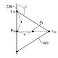
도2의 점선 사각형 부분(A)의 확대도가 도6에 도시된다. d는 두 개의 인접한 관통홀(P2) 사이의 거리를 나타낸다. 도6에 도시된 바와 같이, 관통홀(P2)의 측벽에는 고저항층(500)이 형성되어 있다. x는 제1라인(220)과 관통홀(P2) 사이의 거리를 나타낸다. P2h는 관통홀(P2)로부터 제1라인(220)에 내린 수선의 발을 나타낸다. J13은 하부전극 분리홈(P1)과 상부 분리홈(P3)이 분기되는 점을 나타낸다. r은 상기 P2h와 J13 사이의 거리를 나타낸다.An enlarged view of the dotted rectangle portion A in FIG. 2 is shown in FIG. d represents the distance between two adjacent through holes P2. As shown in FIG. 6, a
도6에 도시된 바와 같이, 제2라인(420)은 상기 관통홀(P2)을 둘러싸는 영역을 제외하고는 제1라인(220)과 겹친다. 즉, 상기 제2라인(420)은 상기 수선의 발(P2h)로부터 제1라인(220) 상의 소정의 거리(r)만큼 떨어진 지점(J13)부터 제1라인(220)으로부터 분기되어 상기 관통홀(P2)을 둘러싸며 상기 수선의 발(P2h)로부터 상기 제1라인(220) 상의 소정의 거리(r)만큼 떨어진 타지점으로 회귀한다.As illustrated in FIG. 6, the
이때, 상기 제2라인(420)이 상기 제1라인(200)으로부터 가장 먼 최외곽 지점(P3p)과 상기 수선의 발(P2h)의 중간에 위치할 수 있으며, 상기 제2라인(420)과 상기 수선의 발(P2h) 사이의 거리는 2x로 나타낼 수 있다.In this case, the
상기 거리(2x)는 종래의 도1에 도시된 것과 같은 광기전력 모듈의 하부전극 분리홈(P1)과 상부 분리홈(P3) 사이의 거리로 제작될 수 있으며, 이 경우 상기 거리(2x)는 200㎛ 이상 300㎛ 이하일 수 있다.The distance 2x may be manufactured as a distance between the lower electrode separation groove P1 and the upper separation groove P3 of the photovoltaic module as shown in FIG. 1, in which case the distance 2x is It may be 200 µm or more and 300 µm or less.
본 발명의 실시예에 따른 광기전력 모듈에서, 상기 관통홀(P2) 사이의 거리(d)는 1mm 이상 5cm 이하인 것이 바람직하다. 이때, 상기 관통홀(P2) 사이의 거리(d)에 대한 상기 거리(2x), 즉 상기 제2라인(420)과 상기 수선의 발(P2h) 사이의 거리에 대한 비율은 4x10⁻³이상 300x10-3이하일 수 있다. 상기 거리(d)가 1mm 보다 작은 경우 무효영역이 증가하므로 충분한 전류 상승의 효과를 얻을 수 없고 제조시간이 증가할 수 있다. 상기 거리(d)가 5cm 보다 큰 경우 전자가 하부전극까지 이동해야 하는 경로가 증가하며, 이에 따라 저항 및 줄열이 커져 광기전력 모듈의 필팩터(fill factor)가 감소할 수 있다.In the photovoltaic module according to an embodiment of the present invention, the distance d between the through holes P2 is preferably 1 mm or more and 5 cm or less. At this time, the ratio of the distance between the through-hole (P2), the distance (2x) of the distance (d) between, that is, the
본 발명의 실시예에 따른 광기전력 모듈의 단위 셀들(UC1, UC2)은 6mm 이상 15mm이하의 폭을 갖는다. 상기 셀 폭이 6mm 보다 작으면 무효 영역이 증가하고 하나의 모듈 당 발생하는 개방 전압(Voc)의 값이 커져 설치 단가가 증가한다. 상기 셀 폭이 15mm 보다 큰 경우 저항이 커져 효율이 감소한다.The unit cells UC1 and UC2 of the photovoltaic module according to the embodiment of the present invention have a width of 6 mm or more and 15 mm or less. If the cell width is smaller than 6 mm, the invalid area is increased and the value of the open voltage Voc generated per one module is increased, thereby increasing the installation cost. If the cell width is larger than 15 mm, the resistance becomes large and efficiency decreases.
상기 상부 분리홈(P3)이 상기 하부전극 분리홈(P1) 위를 지나는 영역, 즉 상기 제1라인(220) 및 상기 제2라인(420)이 중첩되는 부분에서는 직선형 레이저 스크라이빙에 의한 무효영역은 무시할 수 있다. 따라서, 본 발명의 실시예에 따른 집적형 박막 광기전력 모듈에서 레이저 스크라이빙에 의한 무효영역은 상기 상부 분리홈(P3)이 관통홀(P2)을 둘러싸는 영역으로 간주될 수 있다. 본 발명의 실시예에 따른 광기전력 모듈에서 유효 영역에 대한 레이저 스크라이빙에 의한 무효영역의 비는 대략 0.007% 이상 및 1.5% 이하의 값을 가질 수 있다.In the area where the upper separation groove P3 passes over the lower electrode separation groove P1, that is, the portion where the
본 발명의 실시예에 따른 광기전력 모듈에서, 상기 제2라인(420)이 상기 관통홀(P2)을 둘러싸는 형상은 상기 관통홀(P2)로부터 상기 제2라인(420)까지 전자가 이동하는 거리가 가능한 짧도록 결정될 수 있다. 상기 관통홀(P2)로부터 이를 둘러싸는 상부 분리홈(P3)까지의 이동 거리가 짧아야 열 발생을 최소화할 수 있다. 또한, 상기 형상은 관통홀(P2)로부터의 거리가 균등하게 형성하여 이로부터 발생하는 무효 영역을 최소화할 수 있다. 예컨대, 상기 관통홀(P2)을 둘러싸는 상기 상부 분리홈(P3)은 원의 일부의 형태를 가질 수 있다. 예컨대, 상기 제2라인(420)은 부분적인 원의 형태로 상기 관통홀(P2)을 둘러싼다.In the photovoltaic module according to an embodiment of the present invention, the shape in which the
도7a 내지 도7c는 본 발명의 실시예에 따른 광기전력 모듈에서 상기 상부 분리홈(P3)이 상기 관통홀(P2)을 둘러싸는 형상에 대한 다른 예를 도시한다.7A to 7C illustrate another example of a shape in which the upper separation groove P3 surrounds the through hole P2 in the photovoltaic module according to the embodiment of the present invention.
도7a는 제2라인(420)이 제1라인(220)으로부터 분기점(J13)에서 분기되어 타원의 일부를 따라 관통홀(P2)을 둘러싸는 것을 도시한다. 이때, 상기 관통홀(P2)은 수선의 발(P2h)과 상기 제2라인(420)의 최외곽 지점(P3p)의 중간에 위치할 수 있다. 제2라인(420)이 타원 또는 원의 일부를 따라 상기 관통홀(P2)을 둘러싸는 경우에, 상기 관통홀(P2)로부터 상기 제2라인(420)에 이르는 거리가 다소 균일하며 또한 무효영역을 감소시킬 수 있다.FIG. 7A shows that the
도7b 및 도7c에는 상기 제2라인(420)이 상기 관통홀(P2)을 둘러싸는 형태로서 부분적인 오각형 및 삼각형을 예시하고 있다. 이러한 형상으로 상기 제2라인(420)이 상기 관통홀(P2)을 둘러싸는 경우에도, 무효영역을 감소시킬 수 있으며 상기 관통홀(P2)로부터 상기 제2라인(420)에 이르는 거리가 어느 정도 균일함을 알 수 있다.7B and 7C illustrate a partial pentagon and a triangle as the
하지만, 도시된 형상은 단지 예시일 뿐이며, 본 발명의 실시예에 따른 광기전력 모듈에서 상기 특정형상은 오각형, 또는 삼각형을 포함하는 다각형의 일부일 수 있다. 이때, 상기 다각형의 모든 내각은 180°보다 작아야 무효 영역을 효율적으로 감소시킬 수 있다. 또한, 상기 다각형은 상기 수선의 발(P2h), 상기 관통홀(P2) 및 상기 최외곽 지점(P3p)을 잇는 직선에 대해 대칭인 것이 바람직하다. 또한, 상기 다각형의 모든 내각은 90°이상인 것이 바람직한바, 이는 상기 다각형의 내각이 예각을 이루는 경우 동일 꼭지점에서 레이저 빔이 집중되어 과도한 패터닝이 이루어지거나 열에 의해 광전변환층 및 전극층이 손상될 수 있다.However, the shape shown is merely an example, and in the photovoltaic module according to an embodiment of the present invention, the specific shape may be a part of a polygon including a pentagon or a triangle. At this time, all the interior angles of the polygon should be smaller than 180 ° to effectively reduce the invalid area. In addition, the polygon is preferably symmetrical with respect to a straight line connecting the foot P2h of the waterline, the through hole P2 and the outermost point P3p. In addition, it is preferable that all interior angles of the polygons are greater than or equal to 90 °. If the interior angles of the polygons form an acute angle, the laser beam may be concentrated at the same vertex, resulting in excessive patterning or damage of the photoelectric conversion layer and the electrode layer by heat. .
다만, 상기 제1라인(220)과 상기 제2라인(420)이 상기 분기점(J13)에서 이루는 각(θ)은 90°이상 및 135°이하의 값을 가질 수 있다. 예컨대, 상기 형상이 원 또는 타원의 일부인 경우 상기 원 또는 타원의 상기 분기점(J13)에서의 접선과 상기 제1라인(220)이 이루는 각은 90°이상 및 135°이하의 값을 갖는다. 상기 형상이 전술한 다각형인 경우 상기 분기점(J123)에서 상기 다각형의 외각은 90°이상 및 135°이하의 값을 가질 수 있다. 상기 각(θ)이 90°보다 작은 경우 상기 제2라인(420)과 상기 관통홀(P2) 사이의 거리가 멀어지고 무효영역을 효율적으로 감소시키지 못한다. 또한, 상기 각(θ)이 135°보다 큰 경우에도 상기 관통홀(P2)을 둘러싸는 상기 제2라인(420)의 너비가 넓어져 무효 영역을 감소시키는 효과가 저하된다.However, the angle θ formed between the
또한, 상기 관통홀(P2)을 둘러싸는 형상의 모양에 따라 상기 관통홀(P2)의 포인트 형상 또한 원형, 타원형 또는 다각형의 형상을 가질 수 있다. 이러한 관통홀(P2)의 형상은 상기 레이저 가공기에 상기 호모지나이저를 통과한 레이저 빔이 선택적으로 투과될 수 있도록 소정의 패턴이 형성된 마스크를 포함하도록 함으로써 구현할 수 있다. 이와 같이 상기 관통홀(P2)의 형상을 상기 관통홀(P2)을 둘러싸는 형상과 매칭시킴으로써 상기 관통홀(P2)로부터 전자가 하부전극을 통해 이를 둘러싸는 상기 제2라인(420)까지 이르는 거리를 감소시키고 또한 균일하게 할 수 있다.In addition, depending on the shape of the shape surrounding the through hole P2, the point shape of the through hole P2 may also have a circular, elliptical or polygonal shape. The shape of the through hole P2 may be realized by including a mask having a predetermined pattern so that the laser beam passing through the homogenizer may be selectively transmitted to the laser processor. As such, by matching the shape of the through-hole P2 with the shape surrounding the through-hole P2, the distance from the through-hole P2 to the
이상 첨부된 도면을 참조하여 본 발명의 실시예를 설명하였지만, 본 발명이 속하는 기술분야의 당업자는 본 발명이 그 기술적 사상이나 필수적 특징을 변경하지 않고 다른 구체적인 형태로 실시될 수 있다는 것을 이해할 수 있을 것이다. 그러므로 이상에서 기술한 실시예들은 모든 면에서 예시적인 것이며 한정적인 것이 아닌 것으로서 이해되어야 하고, 본 발명의 범위는 상기 상세한 설명보다는 후술하는 특허청구범위에 의하여 나타내어지며, 특허청구범위의 의미 및 범위 그리고 그 등가개념으로부터 도출되는 모든 변경 또는 변형된 형태가 본 발명의 범위에 포함되는 것으로 해석되어야 한다.While the present invention has been particularly shown and described with reference to exemplary embodiments thereof, it is evident that many alternatives, modifications and variations will be apparent to those skilled in the art. will be. Therefore, it should be understood that the above-described embodiments are to be considered in all respects as illustrative and not restrictive, the scope of the invention being indicated by the appended claims rather than the foregoing description, It is intended that all changes and modifications derived from the equivalent concept be included within the scope of the present invention.
100: 기판
200: 하부전극
220: 제1라인
300: 광전변환층
310: 제1단위전지층
320: 중간반사막
330: 제2단위전지층
400: 상부전극
420: 제2라인
500: 고저항층100: substrate
200: lower electrode
220: First line
300: photoelectric conversion layer
310: first unit cell layer
320: middle reflective film
330: second unit cell layer
400: upper electrode
420: second line
500: high resistance layer
Claims (27)
Translated fromKorean상기 제1셀 및 상기 제2 셀은 서로 인접하여 관통홀을 통해 직렬 연결되어 있으며,
상기 제1셀의 하부전극과 상기 제2셀의 하부전극은 하부전극 분리홈에 의해 분리되고,
상기 관통홀은 상기 제2셀의 광전변환층을 관통하는 구멍으로 서로 이격되어 복수개가 형성되어 있고, 상기 관통홀을 통하여 상기 제2셀의 상부전극과 상기 제1셀의 하부전극이 전기적으로 접속되며,
상기 관통홀의 측벽에는 고저항층이 형성되어 있는
집적 광기전력 모듈.An integrated photovoltaic module comprising a lower electrode on a substrate, a photoelectric conversion layer on the lower electrode and including a plurality of unit cell layers, and first and second cells on which the upper electrode is positioned. In
The first cell and the second cell are adjacent to each other are connected in series through a through hole,
The lower electrode of the first cell and the lower electrode of the second cell are separated by the lower electrode separation groove,
The through-holes are spaced apart from each other by holes passing through the photoelectric conversion layer of the second cell, and a plurality of through-holes are electrically connected between the upper electrode of the second cell and the lower electrode of the first cell. ,
The high resistance layer is formed on the sidewall of the through hole.
Integrated photovoltaic modules.
상기 제1셀 및 상기 제2셀은 상기 광전변환층과 상기 상부전극 사이에 투명 전극층을 더 포함하며, 상기 관통홀은 상기 제2셀의 광전변환층 및 투명 전극층에 형성되어 있는 것을 특징으로 하는 집적 광기전력 모듈.The method of claim 1,
The first cell and the second cell further comprises a transparent electrode layer between the photoelectric conversion layer and the upper electrode, wherein the through hole is formed in the photoelectric conversion layer and the transparent electrode layer of the second cell. Integrated photovoltaic module.
상기 제1셀의 광전변환층 및 상부전극과 상기 제2셀의 광전변환층 및 상부전극은 상부 분리홈에 의해서 분리되며,
상기 상부 분리홈은 상기 제1 및 제2 셀의 광전변환층 및 상부전극을 관통하고 상기 하부전극 분리홈과 중첩하도록 형성하되, 상기 상부 분리홈의 일부가 상기 하부전극 분리홈을 벗어나 상기 관통홀을 둘러싸도록 하는 것을 특징으로 하는 집적 광기전력 모듈.The method of claim 1,
The photoelectric conversion layer and the upper electrode of the first cell and the photoelectric conversion layer and the upper electrode of the second cell are separated by an upper separation groove,
The upper separation grooves are formed to penetrate the photoelectric conversion layers and the upper electrodes of the first and second cells and overlap the lower electrode separation grooves, and a part of the upper separation grooves is separated from the lower electrode separation grooves. Integrated photovoltaic module, characterized in that to surround.
상기 제1셀의 광전변환층, 투명전극층 및 상부전극과 상기 제2셀의 광전변환층, 투명전극층 및 상부전극은 상부 분리홈에 의해서 분리되며,
상기 상부 분리홈은 상기 제1 및 제2 셀의 광전변환층, 상기 투명전극층 및 상부전극을 관통하고 상기 하부전극 분리홈과 중첩하도록 형성하되, 상기 상부 분리홈의 일부가 상기 하부전극 분리홈을 벗어나 상기 관통홀을 둘러싸도록 하는 것을 특징으로 하는 집적 광기전력 모듈.3. The method of claim 2,
The photoelectric conversion layer, the transparent electrode layer and the upper electrode of the first cell and the photoelectric conversion layer, the transparent electrode layer and the upper electrode of the second cell are separated by an upper separation groove,
The upper separation grooves are formed to penetrate the photoelectric conversion layers, the transparent electrode layers, and the upper electrodes of the first and second cells, and overlap the lower electrode separation grooves, and a portion of the upper separation grooves may form the lower electrode separation grooves. Integrated photovoltaic module characterized in that it is to surround the through-hole.
상기 하부전극 분리홈과 상기 상부 분리홈 중 하나의 분리홈은 직선 형태를 갖는 것을 특징으로 하는 집적 광기전력 모듈.The method according to claim 3 or 4,
Wherein one of the lower electrode separation groove and the upper separation groove has a linear shape.
상기 고저항층은 상기 광전변환층의 pn 터널접합부가 노출된 상기 관통홀의 측벽에 형성되어 있는 것을 특징으로 하는 집적 광기전력 모듈.The method according to claim 3 or 4,
And the high resistance layer is formed on sidewalls of the through-holes where the pn tunnel junction of the photoelectric conversion layer is exposed.
상기 하부전극 분리홈의 길이에 대한 상기 상부 분리홈과 상기 하부전극 분리홈이 중첩되는 길이의 비는 0.70 이상 0.96 이하인 것을 특징으로 하는 집적 광기전력 모듈.The method of claim 5,
And a ratio of the length of the upper electrode separation groove and the lower electrode separation groove overlapping the length of the lower electrode separation groove is 0.70 or more and 0.96 or less.
상기 상부 분리홈이 상기 하부전극 분리홈 위를 지나지 않는 영역에서 상기 하부전극 분리홈과 상기 상부 분리홈 중 다른 하나의 분리홈은 부분적인 원 또는 타원의 형태를 갖는 것을 특징으로 하는 집적 광기전력 모듈.The method of claim 5,
Wherein the lower electrode separating groove and the other separating groove of the upper electrode separating groove have a shape of a partial circle or an ellipse in a region where the upper separating groove does not pass over the lower electrode separating groove. .
상기 다른 하나의 분리홈이 상기 직선으로부터 분기되는 분기점에서 상기 원 또는 타원의 접선과 상기 직선이 이루는 각은 90°이상 135°이하인 것을 특징으로 하는 집적 광기전력 모듈.9. The method of claim 8,
And an angle formed by the tangent of the circle or ellipse and the straight line at a diverging point at which the other separating groove branches from the straight line is 90 ° or more and 135 ° or less.
상기 상부 분리홈이 상기 하부전극 분리홈 위를 지나가지 않는 영역에서 상기 하부전극 분리홈과 상기 상부 분리홈 중 다른 하나의 분리홈은 부분적인 다각형의 형태를 갖는 것을 특징으로 하는 집적 광기전력 모듈.The method of claim 5,
And the other one of the lower electrode separation groove and the upper separation groove has a partial polygonal shape in a region where the upper separation groove does not pass over the lower electrode separation groove.
상기 다른 하나의 분리홈이 상기 직선으로부터 분기되는 분기점에서 상기 다각형의 외각은 90°이상 135°이하이며,
상기 다각형의 모든 내각은 180° 미만인 것을 특징으로 하는 집적 광기전력 모듈.The method of claim 10,
The outer angle of the polygon at the branching point where the other separation groove is diverged from the straight line is 90 ° or more and 135 ° or less,
Integrated photovoltaic module, characterized in that all of the interior angle of the polygon is less than 180 °.
상기 관통홀은, 상기 상부 분리홈이 상기 하부전극 분리홈 위를 지나지 않는 영역에서 상기 직선상에 내린 상기 관통홀의 수선의 발과 상기 상부 분리홈과 상기 하부전극 분리홈 중 다른 하나의 분리홈의 최외곽 지점 사이의 중심에 위치하는 것을 특징으로 하는 집적 광기전력 모듈.The method of claim 5,
The through hole may be formed by the male foot of the through hole lowered on the straight line and the other one of the upper separation groove and the lower electrode separation groove in an area where the upper separation groove does not pass on the lower electrode separation groove. Integrated photovoltaic module, characterized in that located in the center between the outermost point.
상기 제1셀 및 제2셀 각각의 폭은 6mm 이상 15mm 이하인 것을 특징으로 하는 집적 광기전력 모듈.The method according to claim 3 or 4,
Integrated photovoltaic module, characterized in that the width of each of the first cell and the second cell is 6mm or more and 15mm or less.
상기 관통홀 중 인접한 두 개의 관통홀 사이의 거리는 1mm 이상 5cm 이하인 것을 특징으로 하는 집적 광기전력 모듈.The method according to claim 3 or 4,
Integrated photovoltaic module, characterized in that the distance between two adjacent through holes of the through hole is 1mm or more and 5cm or less.
상기 집적 광기전력 모듈에서 유효 영역에 대한 상기 하부전극 분리홈, 상기 관통홀 및 상기 상부 분리홈에 의한 무효 영역의 비는 0.007% 이상 1.5% 이하인 것을 특징으로 하는 집적 광기전력 모듈.The method according to claim 3 or 4,
And a ratio of an invalid area formed by the lower electrode separation groove, the through hole, and the upper separation groove to an effective area in the integrated photovoltaic module is 0.007% or more and 1.5% or less.
상기 관통홀 중 인접한 두 개의 관통홀은 소정의 거리로 이격되어 있으며,
상기 소정의 거리에 대한 상기 직선상에 내린 상기 관통홀의 수선의 발과 상기 상부 분리홈과 상기 하부전극 분리홈 중 다른 하나의 분리홈의 최외곽 지점 사이의 거리의 비는 4x10⁻³이상 300x10-3이하인 것을 특징으로 하는 집적 광기전력 모듈.The method of claim 5,
Two adjacent through holes of the through holes are spaced apart by a predetermined distance,
The ratio of the distance between the predetermined distance to the straight line of the through-hole perpendicular to the upper separation groove and the lower electrode separation grooves of the other of the separation groove of the outermost point of the down for a 4x10⁻³ is at least 300x10- Integrated photovoltaic module, characterized in that3 or less.
상기 관통홀의 단면의 형상은 원, 타원 또는 다각형인 것을 특징으로 하는 집적 광기전력 모듈.The method according to claim 3 or 4,
Integrated photovoltaic module, characterized in that the cross-sectional shape of the through hole is a circle, ellipse or polygon.
상기 하부전극 분리홈, 상기 관통홀 및 상기 상부 분리홈 중 적어도 하나의 폭에 대한 바닥면의 단차의 비는 5% 이상 및 10%이하인 것을 특징으로 하는 집적 광기전력 모듈.The method according to claim 3 or 4,
And the ratio of the step height of the bottom surface to the width of at least one of the lower electrode separation groove, the through hole and the upper separation groove is 5% or more and 10% or less.
상기 광전변환층은 상기 복수의 단위전지층 사이에 적어도 하나의 중간반사막을 포함하며,
상기 고저항층은 상기 중간반사막이 노출된 상기 관통홀의 측벽에 형성되어 있는 것을 특징으로 하는 집적 광기전력 모듈.The method according to claim 3 or 4,
The photoelectric conversion layer includes at least one intermediate reflective film between the plurality of unit cell layers,
And the high resistance layer is formed on sidewalls of the through-holes in which the intermediate reflection film is exposed.
상기 하부전극층을 제1셀 하부전극층 및 제2셀 하부전극층으로 분리하는 하부전극 분리홈을 형성하는 단계;
상기 제1셀 및 제2셀 하부전극층 상에 복수의 단위전지층을 포함하는 광전변환층을 형성하는 단계;
상기 제2셀 하부전극층상의 광전변환층을 관통하는 서로 이격된 복수의 관통홀을 상기 하부전극 분리홈의 일 측에 형성하는 단계;
상기 관통홀의 측벽에 고저항층을 형성하는 단계;
상기 관통홀 내부 및 상기 광전변환층 상에 상부전극층을 형성하는 단계; 및
상기 상부전극층 및 상기 광전변환층을 분리하는 상부 분리홈을 상기 하부전극 분리홈과 중첩하도록 형성하되, 상기 상부 분리홈의 일부가 상기 하부전극 분리홈을 벗어나 상기 관통홀을 둘러싸도록 형성하는 단계;
를 포함하는 집적 광기전력 모듈 제조방법.Forming a lower electrode layer on the substrate;
Forming a lower electrode separation groove separating the lower electrode layer into a first cell lower electrode layer and a second cell lower electrode layer;
Forming a photoelectric conversion layer including a plurality of unit battery layers on the first cell and the second cell lower electrode layers;
Forming a plurality of through holes spaced apart from each other through the photoelectric conversion layer on the second cell lower electrode layer on one side of the lower electrode separation groove;
Forming a high resistance layer on sidewalls of the through holes;
Forming an upper electrode layer in the through hole and on the photoelectric conversion layer; And
Forming an upper separation groove that separates the upper electrode layer and the photoelectric conversion layer to overlap the lower electrode separation groove, wherein a portion of the upper separation groove is formed to escape the lower electrode separation groove and surround the through hole;
Integrated photovoltaic module manufacturing method comprising a.
상기 광전변환층을 형성하는 단계 후 및 상기 관통홀을 형성하는 단계 전에 상기 광전변환층 상에 투명 전극층을 형성하는 단계를 더 포함하며,
상기 관통홀을 형성하는 단계는 상기 제2셀 하부전극층상의 광전변환층 및 투명 전극층을 관통하는 서로 이격된 복수의 관통홀을 형성하는 단계인 것을 특징으로 하는 집적 광기전력 모듈 제조방법.21. The method of claim 20,
And forming a transparent electrode layer on the photoelectric conversion layer after forming the photoelectric conversion layer and before forming the through hole.
The forming of the through holes may include forming a plurality of through holes spaced apart from each other through the photoelectric conversion layer and the transparent electrode layer on the second cell lower electrode layer.
상기 하부전극 분리홈, 상기 관통홀 및 상기 상부 분리홈 중 적어도 하나는 레이저 스크라이빙에 의해 형성되는 것을 특징으로 하는 집적 광기전력 모듈 제조방법.22. The method according to claim 20 or 21,
At least one of the lower electrode separation groove, the through hole and the upper separation groove is formed by laser scribing.
상기 관통홀의 측벽에 고저항층을 형성하는 단계는 고저항성 원소를 적어도 하나 이상 포함하는 가스 분위기에서 플라즈마 처리를 함으로써 수행되는 것을 특징으로 하는 집적 광기전력 모듈 제조방법.22. The method according to claim 20 or 21,
Forming a high resistance layer on the sidewall of the through hole is a method of manufacturing an integrated photovoltaic module, characterized in that performed by performing a plasma treatment in a gas atmosphere containing at least one of the high resistance element.
상기 고저항성 원소는 산소, 질소 또는 탄소를 포함하는 것을 특징으로 하는 집적 광기전력 모듈 제조방법.24. The method of claim 23,
The high resistance element is an integrated photovoltaic module manufacturing method characterized in that it comprises oxygen, nitrogen or carbon.
상기 관통홀의 측벽에 고저항층을 형성하는 단계는 물리적 방법 또는 화학적 방법에 따라 상기 관통홀 측벽을 산화시킴으로써 수행되는 것을 특징으로 하는 집적 광기전력 모듈 제조방법.22. The method according to claim 20 or 21,
And forming a high resistance layer on the sidewalls of the through-holes by oxidizing the sidewalls of the through-holes according to a physical method or a chemical method.
상기 관통홀의 측벽에 고저항층을 형성하는 단계는: 상기 고저항층을 상기 광전변환층의 pn 터널접합부가 노출된 상기 관통홀의 측벽에 형성하는 것을 특징으로 하는 집적 광기전력 모듈 제조방법.22. The method according to claim 20 or 21,
The forming of the high resistance layer on the sidewall of the through hole may include: forming the high resistance layer on the sidewall of the through hole exposed to the pn tunnel junction of the photoelectric conversion layer.
상기 광전변환층은 상기 복수의 단위전지층 사이에 적어도 하나의 중간반사막을 포함하며,
상기 관통홀의 측벽에 고저항층을 형성하는 단계는: 상기 고저항층을 상기 중간반사막이 노출된 상기 관통홀의 측벽에 형성하는 것을 특징으로 하는 집적 광기전력 모듈 제조방법.22. The method according to claim 20 or 21,
The photoelectric conversion layer includes at least one intermediate reflective film between the plurality of unit cell layers,
The forming of the high resistance layer on the sidewalls of the through-holes includes: forming the high resistance layer on the sidewalls of the through-holes in which the intermediate reflective film is exposed.
Priority Applications (2)
| Application Number | Priority Date | Filing Date | Title |
|---|---|---|---|
| KR1020110123496AKR101332297B1 (en) | 2011-11-24 | 2011-11-24 | Tandem type Integrated Photovoltaic Module and Manufacturing Method Thereof |
| US13/483,870US9142701B2 (en) | 2011-11-24 | 2012-05-30 | Tandem type integrated photovoltaic module and manufacturing method thereof |
Applications Claiming Priority (1)
| Application Number | Priority Date | Filing Date | Title |
|---|---|---|---|
| KR1020110123496AKR101332297B1 (en) | 2011-11-24 | 2011-11-24 | Tandem type Integrated Photovoltaic Module and Manufacturing Method Thereof |
Publications (2)
| Publication Number | Publication Date |
|---|---|
| KR20130057646A KR20130057646A (en) | 2013-06-03 |
| KR101332297B1true KR101332297B1 (en) | 2013-11-22 |
Family
ID=48857176
Family Applications (1)
| Application Number | Title | Priority Date | Filing Date |
|---|---|---|---|
| KR1020110123496AExpired - Fee RelatedKR101332297B1 (en) | 2011-11-24 | 2011-11-24 | Tandem type Integrated Photovoltaic Module and Manufacturing Method Thereof |
Country Status (2)
| Country | Link |
|---|---|
| US (1) | US9142701B2 (en) |
| KR (1) | KR101332297B1 (en) |
Families Citing this family (1)
| Publication number | Priority date | Publication date | Assignee | Title |
|---|---|---|---|---|
| DE102017122530B4 (en)* | 2017-09-28 | 2023-02-23 | Helmholtz-Zentrum Berlin für Materialien und Energie Gesellschaft mit beschränkter Haftung | Photovoltaic module with interlocking contacts on the back |
Citations (4)
| Publication number | Priority date | Publication date | Assignee | Title |
|---|---|---|---|---|
| JP2002094089A (en) | 2000-09-11 | 2002-03-29 | Honda Motor Co Ltd | Method for manufacturing compound thin film solar cell |
| JP2009049227A (en) | 2007-08-21 | 2009-03-05 | Masayoshi Murata | Integrated multi-junction thin film silicon solar cell module and its manufacturing method |
| KR20090080171A (en)* | 2008-01-21 | 2009-07-24 | 소닉스자펜 주식회사 | Photoelectric Conversion Module Structure and Manufacturing Method for Increasing Photovoltaic Generation Area of Integrated Thin Film Solar Cell |
| JP2011155041A (en) | 2010-01-26 | 2011-08-11 | Kyocera Corp | Solar cell element and solar cell module |
Family Cites Families (7)
| Publication number | Priority date | Publication date | Assignee | Title |
|---|---|---|---|---|
| US6265652B1 (en)* | 1995-06-15 | 2001-07-24 | Kanegafuchi Kagaku Kogyo Kabushiki Kabushiki Kaisha | Integrated thin-film solar battery and method of manufacturing the same |
| JP3815875B2 (en) | 1997-12-24 | 2006-08-30 | 株式会社カネカ | Manufacturing method of integrated thin film photoelectric conversion device |
| JP2002261308A (en)* | 2001-03-01 | 2002-09-13 | Kanegafuchi Chem Ind Co Ltd | Thin-film photoelectric conversion module |
| JP4681352B2 (en)* | 2005-05-24 | 2011-05-11 | 本田技研工業株式会社 | Chalcopyrite solar cell |
| JP4411338B2 (en) | 2007-07-13 | 2010-02-10 | シャープ株式会社 | Thin film solar cell module |
| JP2009065076A (en)* | 2007-09-10 | 2009-03-26 | Masayoshi Murata | Integrated tandem-type thin film silicon solar cell module and manufacturing method thereof |
| US20100147361A1 (en)* | 2008-12-15 | 2010-06-17 | Chen Yung T | Tandem junction photovoltaic device comprising copper indium gallium di-selenide bottom cell |
- 2011
- 2011-11-24KRKR1020110123496Apatent/KR101332297B1/ennot_activeExpired - Fee Related
- 2012
- 2012-05-30USUS13/483,870patent/US9142701B2/ennot_activeExpired - Fee Related
Patent Citations (4)
| Publication number | Priority date | Publication date | Assignee | Title |
|---|---|---|---|---|
| JP2002094089A (en) | 2000-09-11 | 2002-03-29 | Honda Motor Co Ltd | Method for manufacturing compound thin film solar cell |
| JP2009049227A (en) | 2007-08-21 | 2009-03-05 | Masayoshi Murata | Integrated multi-junction thin film silicon solar cell module and its manufacturing method |
| KR20090080171A (en)* | 2008-01-21 | 2009-07-24 | 소닉스자펜 주식회사 | Photoelectric Conversion Module Structure and Manufacturing Method for Increasing Photovoltaic Generation Area of Integrated Thin Film Solar Cell |
| JP2011155041A (en) | 2010-01-26 | 2011-08-11 | Kyocera Corp | Solar cell element and solar cell module |
Also Published As
| Publication number | Publication date |
|---|---|
| KR20130057646A (en) | 2013-06-03 |
| US20130206216A1 (en) | 2013-08-15 |
| US9142701B2 (en) | 2015-09-22 |
Similar Documents
| Publication | Publication Date | Title |
|---|---|---|
| US8525018B2 (en) | Solar cell | |
| US8962985B2 (en) | Solar cell and solar cell module | |
| CN102449780B (en) | Solar battery apparatus and manufacture method thereof | |
| US9871146B2 (en) | Solar cell and method for manufacturing the same | |
| US9202948B2 (en) | Solar cell and method for manufacturing the same | |
| EP2551914B1 (en) | Solar cell and method for manufacturing the same | |
| US20120103416A1 (en) | Solar cell apparatus and method for manufacturing the same | |
| KR101196387B1 (en) | Integrated Thin Film Photovoltaic Module and Manufacturing Method Thereof | |
| KR100999797B1 (en) | Photovoltaic device and its manufacturing method | |
| US20110155210A1 (en) | Solar cell module | |
| US9929297B2 (en) | Solar cell and method for manufacturing the same | |
| KR20110100725A (en) | Solar cell and manufacturing method | |
| KR101699312B1 (en) | Solar cell and manufacturing method thereof | |
| KR20120012325A (en) | Photovoltaic device and its manufacturing method | |
| KR101203452B1 (en) | Tandem Type Integrated Photovoltaic Module and Manufacturing Method Thereof | |
| KR101332297B1 (en) | Tandem type Integrated Photovoltaic Module and Manufacturing Method Thereof | |
| US20130032205A1 (en) | Solar photovoltaic device and a production method therefor | |
| KR101172252B1 (en) | Tandem type Integrated Photovoltaic Module and Manufacturing Method Thereof | |
| KR101226446B1 (en) | Integrated Thin Film Photovoltaic Module and Manufacturing Method Thereof | |
| US20130312816A1 (en) | Tandem type integrated photovoltaic module and manufacturing method thereof | |
| KR20100109313A (en) | Solar cell and method of fabricating the same | |
| US9130102B2 (en) | Integrated thin film photovoltaic module and manufacturing method thereof | |
| KR20100070747A (en) | Photovoltaic device array and method of fabricating the same | |
| KR20130030905A (en) | Solar cell | |
| KR20130019845A (en) | Thin film solar cell module |
Legal Events
| Date | Code | Title | Description |
|---|---|---|---|
| A201 | Request for examination | ||
| PA0109 | Patent application | St.27 status event code:A-0-1-A10-A12-nap-PA0109 | |
| PA0201 | Request for examination | St.27 status event code:A-1-2-D10-D11-exm-PA0201 | |
| D13-X000 | Search requested | St.27 status event code:A-1-2-D10-D13-srh-X000 | |
| D14-X000 | Search report completed | St.27 status event code:A-1-2-D10-D14-srh-X000 | |
| E902 | Notification of reason for refusal | ||
| PE0902 | Notice of grounds for rejection | St.27 status event code:A-1-2-D10-D21-exm-PE0902 | |
| T11-X000 | Administrative time limit extension requested | St.27 status event code:U-3-3-T10-T11-oth-X000 | |
| T11-X000 | Administrative time limit extension requested | St.27 status event code:U-3-3-T10-T11-oth-X000 | |
| PG1501 | Laying open of application | St.27 status event code:A-1-1-Q10-Q12-nap-PG1501 | |
| N231 | Notification of change of applicant | ||
| PN2301 | Change of applicant | St.27 status event code:A-3-3-R10-R13-asn-PN2301 St.27 status event code:A-3-3-R10-R11-asn-PN2301 | |
| T11-X000 | Administrative time limit extension requested | St.27 status event code:U-3-3-T10-T11-oth-X000 | |
| T11-X000 | Administrative time limit extension requested | St.27 status event code:U-3-3-T10-T11-oth-X000 | |
| T11-X000 | Administrative time limit extension requested | St.27 status event code:U-3-3-T10-T11-oth-X000 | |
| T12-X000 | Administrative time limit extension not granted | St.27 status event code:U-3-3-T10-T12-oth-X000 | |
| R17-X000 | Change to representative recorded | St.27 status event code:A-3-3-R10-R17-oth-X000 | |
| AMND | Amendment | ||
| P11-X000 | Amendment of application requested | St.27 status event code:A-2-2-P10-P11-nap-X000 | |
| P13-X000 | Application amended | St.27 status event code:A-2-2-P10-P13-nap-X000 | |
| E601 | Decision to refuse application | ||
| PE0601 | Decision on rejection of patent | St.27 status event code:N-2-6-B10-B15-exm-PE0601 | |
| AMND | Amendment | ||
| P11-X000 | Amendment of application requested | St.27 status event code:A-2-2-P10-P11-nap-X000 | |
| P13-X000 | Application amended | St.27 status event code:A-2-2-P10-P13-nap-X000 | |
| PX0901 | Re-examination | St.27 status event code:A-2-3-E10-E12-rex-PX0901 | |
| PX0701 | Decision of registration after re-examination | St.27 status event code:A-3-4-F10-F13-rex-PX0701 | |
| X701 | Decision to grant (after re-examination) | ||
| GRNT | Written decision to grant | ||
| PR0701 | Registration of establishment | St.27 status event code:A-2-4-F10-F11-exm-PR0701 | |
| PR1002 | Payment of registration fee | St.27 status event code:A-2-2-U10-U11-oth-PR1002 Fee payment year number:1 | |
| PG1601 | Publication of registration | St.27 status event code:A-4-4-Q10-Q13-nap-PG1601 | |
| P22-X000 | Classification modified | St.27 status event code:A-4-4-P10-P22-nap-X000 | |
| R18-X000 | Changes to party contact information recorded | St.27 status event code:A-5-5-R10-R18-oth-X000 | |
| FPAY | Annual fee payment | Payment date:20161012 Year of fee payment:4 | |
| PR1001 | Payment of annual fee | St.27 status event code:A-4-4-U10-U11-oth-PR1001 Fee payment year number:4 | |
| R18-X000 | Changes to party contact information recorded | St.27 status event code:A-5-5-R10-R18-oth-X000 | |
| R18-X000 | Changes to party contact information recorded | St.27 status event code:A-5-5-R10-R18-oth-X000 | |
| L13-X000 | Limitation or reissue of ip right requested | St.27 status event code:A-2-3-L10-L13-lim-X000 | |
| U15-X000 | Partial renewal or maintenance fee paid modifying the ip right scope | St.27 status event code:A-4-4-U10-U15-oth-X000 | |
| FPAY | Annual fee payment | Payment date:20171030 Year of fee payment:5 | |
| PR1001 | Payment of annual fee | St.27 status event code:A-4-4-U10-U11-oth-PR1001 Fee payment year number:5 | |
| LAPS | Lapse due to unpaid annual fee | ||
| PC1903 | Unpaid annual fee | St.27 status event code:A-4-4-U10-U13-oth-PC1903 Not in force date:20181119 Payment event data comment text:Termination Category : DEFAULT_OF_REGISTRATION_FEE | |
| PN2301 | Change of applicant | St.27 status event code:A-5-5-R10-R13-asn-PN2301 St.27 status event code:A-5-5-R10-R11-asn-PN2301 | |
| PC1903 | Unpaid annual fee | St.27 status event code:N-4-6-H10-H13-oth-PC1903 Ip right cessation event data comment text:Termination Category : DEFAULT_OF_REGISTRATION_FEE Not in force date:20181119 | |
| R18-X000 | Changes to party contact information recorded | St.27 status event code:A-5-5-R10-R18-oth-X000 | |
| P22-X000 | Classification modified | St.27 status event code:A-4-4-P10-P22-nap-X000 |