KR101329285B1 - Formation of high quality dielectric films of silicon dioxide for sti: usage of different siloxane-based precursors for harp ii - remote plasma enhanced deposition processes - Google Patents
Formation of high quality dielectric films of silicon dioxide for sti: usage of different siloxane-based precursors for harp ii - remote plasma enhanced deposition processesDownload PDFInfo
- Publication number
- KR101329285B1 KR101329285B1KR1020097010045AKR20097010045AKR101329285B1KR 101329285 B1KR101329285 B1KR 101329285B1KR 1020097010045 AKR1020097010045 AKR 1020097010045AKR 20097010045 AKR20097010045 AKR 20097010045AKR 101329285 B1KR101329285 B1KR 101329285B1
- Authority
- KR
- South Korea
- Prior art keywords
- delete delete
- oxygen
- organo
- precursor
- silicon
- Prior art date
- Legal status (The legal status is an assumption and is not a legal conclusion. Google has not performed a legal analysis and makes no representation as to the accuracy of the status listed.)
- Active
Links
- 0C*(*C1)*ONS1=CChemical compoundC*(*C1)*ONS1=C0.000description1
Images


Classifications
- C—CHEMISTRY; METALLURGY
- C23—COATING METALLIC MATERIAL; COATING MATERIAL WITH METALLIC MATERIAL; CHEMICAL SURFACE TREATMENT; DIFFUSION TREATMENT OF METALLIC MATERIAL; COATING BY VACUUM EVAPORATION, BY SPUTTERING, BY ION IMPLANTATION OR BY CHEMICAL VAPOUR DEPOSITION, IN GENERAL; INHIBITING CORROSION OF METALLIC MATERIAL OR INCRUSTATION IN GENERAL
- C23C—COATING METALLIC MATERIAL; COATING MATERIAL WITH METALLIC MATERIAL; SURFACE TREATMENT OF METALLIC MATERIAL BY DIFFUSION INTO THE SURFACE, BY CHEMICAL CONVERSION OR SUBSTITUTION; COATING BY VACUUM EVAPORATION, BY SPUTTERING, BY ION IMPLANTATION OR BY CHEMICAL VAPOUR DEPOSITION, IN GENERAL
- C23C16/00—Chemical coating by decomposition of gaseous compounds, without leaving reaction products of surface material in the coating, i.e. chemical vapour deposition [CVD] processes
- C23C16/04—Coating on selected surface areas, e.g. using masks
- C23C16/045—Coating cavities or hollow spaces, e.g. interior of tubes; Infiltration of porous substrates
- C—CHEMISTRY; METALLURGY
- C23—COATING METALLIC MATERIAL; COATING MATERIAL WITH METALLIC MATERIAL; CHEMICAL SURFACE TREATMENT; DIFFUSION TREATMENT OF METALLIC MATERIAL; COATING BY VACUUM EVAPORATION, BY SPUTTERING, BY ION IMPLANTATION OR BY CHEMICAL VAPOUR DEPOSITION, IN GENERAL; INHIBITING CORROSION OF METALLIC MATERIAL OR INCRUSTATION IN GENERAL
- C23C—COATING METALLIC MATERIAL; COATING MATERIAL WITH METALLIC MATERIAL; SURFACE TREATMENT OF METALLIC MATERIAL BY DIFFUSION INTO THE SURFACE, BY CHEMICAL CONVERSION OR SUBSTITUTION; COATING BY VACUUM EVAPORATION, BY SPUTTERING, BY ION IMPLANTATION OR BY CHEMICAL VAPOUR DEPOSITION, IN GENERAL
- C23C16/00—Chemical coating by decomposition of gaseous compounds, without leaving reaction products of surface material in the coating, i.e. chemical vapour deposition [CVD] processes
- C23C16/06—Chemical coating by decomposition of gaseous compounds, without leaving reaction products of surface material in the coating, i.e. chemical vapour deposition [CVD] processes characterised by the deposition of metallic material
- C23C16/18—Chemical coating by decomposition of gaseous compounds, without leaving reaction products of surface material in the coating, i.e. chemical vapour deposition [CVD] processes characterised by the deposition of metallic material from metallo-organic compounds
- C—CHEMISTRY; METALLURGY
- C23—COATING METALLIC MATERIAL; COATING MATERIAL WITH METALLIC MATERIAL; CHEMICAL SURFACE TREATMENT; DIFFUSION TREATMENT OF METALLIC MATERIAL; COATING BY VACUUM EVAPORATION, BY SPUTTERING, BY ION IMPLANTATION OR BY CHEMICAL VAPOUR DEPOSITION, IN GENERAL; INHIBITING CORROSION OF METALLIC MATERIAL OR INCRUSTATION IN GENERAL
- C23C—COATING METALLIC MATERIAL; COATING MATERIAL WITH METALLIC MATERIAL; SURFACE TREATMENT OF METALLIC MATERIAL BY DIFFUSION INTO THE SURFACE, BY CHEMICAL CONVERSION OR SUBSTITUTION; COATING BY VACUUM EVAPORATION, BY SPUTTERING, BY ION IMPLANTATION OR BY CHEMICAL VAPOUR DEPOSITION, IN GENERAL
- C23C16/00—Chemical coating by decomposition of gaseous compounds, without leaving reaction products of surface material in the coating, i.e. chemical vapour deposition [CVD] processes
- C23C16/22—Chemical coating by decomposition of gaseous compounds, without leaving reaction products of surface material in the coating, i.e. chemical vapour deposition [CVD] processes characterised by the deposition of inorganic material, other than metallic material
- C23C16/30—Deposition of compounds, mixtures or solid solutions, e.g. borides, carbides, nitrides
- C23C16/40—Oxides
- C23C16/401—Oxides containing silicon
- C—CHEMISTRY; METALLURGY
- C23—COATING METALLIC MATERIAL; COATING MATERIAL WITH METALLIC MATERIAL; CHEMICAL SURFACE TREATMENT; DIFFUSION TREATMENT OF METALLIC MATERIAL; COATING BY VACUUM EVAPORATION, BY SPUTTERING, BY ION IMPLANTATION OR BY CHEMICAL VAPOUR DEPOSITION, IN GENERAL; INHIBITING CORROSION OF METALLIC MATERIAL OR INCRUSTATION IN GENERAL
- C23C—COATING METALLIC MATERIAL; COATING MATERIAL WITH METALLIC MATERIAL; SURFACE TREATMENT OF METALLIC MATERIAL BY DIFFUSION INTO THE SURFACE, BY CHEMICAL CONVERSION OR SUBSTITUTION; COATING BY VACUUM EVAPORATION, BY SPUTTERING, BY ION IMPLANTATION OR BY CHEMICAL VAPOUR DEPOSITION, IN GENERAL
- C23C16/00—Chemical coating by decomposition of gaseous compounds, without leaving reaction products of surface material in the coating, i.e. chemical vapour deposition [CVD] processes
- C23C16/44—Chemical coating by decomposition of gaseous compounds, without leaving reaction products of surface material in the coating, i.e. chemical vapour deposition [CVD] processes characterised by the method of coating
- C23C16/448—Chemical coating by decomposition of gaseous compounds, without leaving reaction products of surface material in the coating, i.e. chemical vapour deposition [CVD] processes characterised by the method of coating characterised by the method used for generating reactive gas streams, e.g. by evaporation or sublimation of precursor materials
- C23C16/452—Chemical coating by decomposition of gaseous compounds, without leaving reaction products of surface material in the coating, i.e. chemical vapour deposition [CVD] processes characterised by the method of coating characterised by the method used for generating reactive gas streams, e.g. by evaporation or sublimation of precursor materials by activating reactive gas streams before their introduction into the reaction chamber, e.g. by ionisation or addition of reactive species
- C—CHEMISTRY; METALLURGY
- C23—COATING METALLIC MATERIAL; COATING MATERIAL WITH METALLIC MATERIAL; CHEMICAL SURFACE TREATMENT; DIFFUSION TREATMENT OF METALLIC MATERIAL; COATING BY VACUUM EVAPORATION, BY SPUTTERING, BY ION IMPLANTATION OR BY CHEMICAL VAPOUR DEPOSITION, IN GENERAL; INHIBITING CORROSION OF METALLIC MATERIAL OR INCRUSTATION IN GENERAL
- C23C—COATING METALLIC MATERIAL; COATING MATERIAL WITH METALLIC MATERIAL; SURFACE TREATMENT OF METALLIC MATERIAL BY DIFFUSION INTO THE SURFACE, BY CHEMICAL CONVERSION OR SUBSTITUTION; COATING BY VACUUM EVAPORATION, BY SPUTTERING, BY ION IMPLANTATION OR BY CHEMICAL VAPOUR DEPOSITION, IN GENERAL
- C23C16/00—Chemical coating by decomposition of gaseous compounds, without leaving reaction products of surface material in the coating, i.e. chemical vapour deposition [CVD] processes
- C23C16/44—Chemical coating by decomposition of gaseous compounds, without leaving reaction products of surface material in the coating, i.e. chemical vapour deposition [CVD] processes characterised by the method of coating
- C23C16/455—Chemical coating by decomposition of gaseous compounds, without leaving reaction products of surface material in the coating, i.e. chemical vapour deposition [CVD] processes characterised by the method of coating characterised by the method used for introducing gases into reaction chamber or for modifying gas flows in reaction chamber
- C23C16/45523—Pulsed gas flow or change of composition over time
- C23C16/45525—Atomic layer deposition [ALD]
- C23C16/45553—Atomic layer deposition [ALD] characterized by the use of precursors specially adapted for ALD
- H—ELECTRICITY
- H01—ELECTRIC ELEMENTS
- H01L—SEMICONDUCTOR DEVICES NOT COVERED BY CLASS H10
- H01L21/00—Processes or apparatus adapted for the manufacture or treatment of semiconductor or solid state devices or of parts thereof
- H01L21/02—Manufacture or treatment of semiconductor devices or of parts thereof
- H01L21/02104—Forming layers
- H01L21/02107—Forming insulating materials on a substrate
- H01L21/02109—Forming insulating materials on a substrate characterised by the type of layer, e.g. type of material, porous/non-porous, pre-cursors, mixtures or laminates
- H01L21/022—Forming insulating materials on a substrate characterised by the type of layer, e.g. type of material, porous/non-porous, pre-cursors, mixtures or laminates the layer being a laminate, i.e. composed of sublayers, e.g. stacks of alternating high-k metal oxides
- H—ELECTRICITY
- H01—ELECTRIC ELEMENTS
- H01L—SEMICONDUCTOR DEVICES NOT COVERED BY CLASS H10
- H01L21/00—Processes or apparatus adapted for the manufacture or treatment of semiconductor or solid state devices or of parts thereof
- H01L21/02—Manufacture or treatment of semiconductor devices or of parts thereof
- H01L21/02104—Forming layers
- H01L21/02107—Forming insulating materials on a substrate
- H01L21/02296—Forming insulating materials on a substrate characterised by the treatment performed before or after the formation of the layer
- H01L21/02318—Forming insulating materials on a substrate characterised by the treatment performed before or after the formation of the layer post-treatment
- H01L21/02337—Forming insulating materials on a substrate characterised by the treatment performed before or after the formation of the layer post-treatment treatment by exposure to a gas or vapour
- H01L21/0234—Forming insulating materials on a substrate characterised by the treatment performed before or after the formation of the layer post-treatment treatment by exposure to a gas or vapour treatment by exposure to a plasma
- H—ELECTRICITY
- H01—ELECTRIC ELEMENTS
- H01L—SEMICONDUCTOR DEVICES NOT COVERED BY CLASS H10
- H01L21/00—Processes or apparatus adapted for the manufacture or treatment of semiconductor or solid state devices or of parts thereof
- H01L21/02—Manufacture or treatment of semiconductor devices or of parts thereof
- H01L21/02104—Forming layers
- H01L21/02107—Forming insulating materials on a substrate
- H01L21/02296—Forming insulating materials on a substrate characterised by the treatment performed before or after the formation of the layer
- H01L21/02318—Forming insulating materials on a substrate characterised by the treatment performed before or after the formation of the layer post-treatment
- H01L21/02345—Forming insulating materials on a substrate characterised by the treatment performed before or after the formation of the layer post-treatment treatment by exposure to radiation, e.g. visible light
- H01L21/02348—Forming insulating materials on a substrate characterised by the treatment performed before or after the formation of the layer post-treatment treatment by exposure to radiation, e.g. visible light treatment by exposure to UV light
- H—ELECTRICITY
- H01—ELECTRIC ELEMENTS
- H01L—SEMICONDUCTOR DEVICES NOT COVERED BY CLASS H10
- H01L21/00—Processes or apparatus adapted for the manufacture or treatment of semiconductor or solid state devices or of parts thereof
- H01L21/02—Manufacture or treatment of semiconductor devices or of parts thereof
- H01L21/04—Manufacture or treatment of semiconductor devices or of parts thereof the devices having potential barriers, e.g. a PN junction, depletion layer or carrier concentration layer
- H01L21/18—Manufacture or treatment of semiconductor devices or of parts thereof the devices having potential barriers, e.g. a PN junction, depletion layer or carrier concentration layer the devices having semiconductor bodies comprising elements of Group IV of the Periodic Table or AIIIBV compounds with or without impurities, e.g. doping materials
- H01L21/30—Treatment of semiconductor bodies using processes or apparatus not provided for in groups H01L21/20 - H01L21/26
- H01L21/31—Treatment of semiconductor bodies using processes or apparatus not provided for in groups H01L21/20 - H01L21/26 to form insulating layers thereon, e.g. for masking or by using photolithographic techniques; After treatment of these layers; Selection of materials for these layers
- H01L21/3105—After-treatment
- H01L21/311—Etching the insulating layers by chemical or physical means
- H01L21/31105—Etching inorganic layers
- H01L21/31111—Etching inorganic layers by chemical means
- H01L21/31116—Etching inorganic layers by chemical means by dry-etching
- H—ELECTRICITY
- H01—ELECTRIC ELEMENTS
- H01L—SEMICONDUCTOR DEVICES NOT COVERED BY CLASS H10
- H01L21/00—Processes or apparatus adapted for the manufacture or treatment of semiconductor or solid state devices or of parts thereof
- H01L21/70—Manufacture or treatment of devices consisting of a plurality of solid state components formed in or on a common substrate or of parts thereof; Manufacture of integrated circuit devices or of parts thereof
- H01L21/71—Manufacture of specific parts of devices defined in group H01L21/70
- H01L21/76—Making of isolation regions between components
- H01L21/762—Dielectric regions, e.g. EPIC dielectric isolation, LOCOS; Trench refilling techniques, SOI technology, use of channel stoppers
- H01L21/76224—Dielectric regions, e.g. EPIC dielectric isolation, LOCOS; Trench refilling techniques, SOI technology, use of channel stoppers using trench refilling with dielectric materials
- H—ELECTRICITY
- H01—ELECTRIC ELEMENTS
- H01L—SEMICONDUCTOR DEVICES NOT COVERED BY CLASS H10
- H01L21/00—Processes or apparatus adapted for the manufacture or treatment of semiconductor or solid state devices or of parts thereof
- H01L21/02—Manufacture or treatment of semiconductor devices or of parts thereof
- H01L21/02104—Forming layers
- H01L21/02107—Forming insulating materials on a substrate
- H01L21/02109—Forming insulating materials on a substrate characterised by the type of layer, e.g. type of material, porous/non-porous, pre-cursors, mixtures or laminates
- H01L21/02112—Forming insulating materials on a substrate characterised by the type of layer, e.g. type of material, porous/non-porous, pre-cursors, mixtures or laminates characterised by the material of the layer
- H01L21/02123—Forming insulating materials on a substrate characterised by the type of layer, e.g. type of material, porous/non-porous, pre-cursors, mixtures or laminates characterised by the material of the layer the material containing silicon
- H01L21/02126—Forming insulating materials on a substrate characterised by the type of layer, e.g. type of material, porous/non-porous, pre-cursors, mixtures or laminates characterised by the material of the layer the material containing silicon the material containing Si, O, and at least one of H, N, C, F, or other non-metal elements, e.g. SiOC, SiOC:H or SiONC
- H—ELECTRICITY
- H01—ELECTRIC ELEMENTS
- H01L—SEMICONDUCTOR DEVICES NOT COVERED BY CLASS H10
- H01L21/00—Processes or apparatus adapted for the manufacture or treatment of semiconductor or solid state devices or of parts thereof
- H01L21/02—Manufacture or treatment of semiconductor devices or of parts thereof
- H01L21/02104—Forming layers
- H01L21/02107—Forming insulating materials on a substrate
- H01L21/02109—Forming insulating materials on a substrate characterised by the type of layer, e.g. type of material, porous/non-porous, pre-cursors, mixtures or laminates
- H01L21/02112—Forming insulating materials on a substrate characterised by the type of layer, e.g. type of material, porous/non-porous, pre-cursors, mixtures or laminates characterised by the material of the layer
- H01L21/02123—Forming insulating materials on a substrate characterised by the type of layer, e.g. type of material, porous/non-porous, pre-cursors, mixtures or laminates characterised by the material of the layer the material containing silicon
- H01L21/02164—Forming insulating materials on a substrate characterised by the type of layer, e.g. type of material, porous/non-porous, pre-cursors, mixtures or laminates characterised by the material of the layer the material containing silicon the material being a silicon oxide, e.g. SiO2
- H—ELECTRICITY
- H01—ELECTRIC ELEMENTS
- H01L—SEMICONDUCTOR DEVICES NOT COVERED BY CLASS H10
- H01L21/00—Processes or apparatus adapted for the manufacture or treatment of semiconductor or solid state devices or of parts thereof
- H01L21/02—Manufacture or treatment of semiconductor devices or of parts thereof
- H01L21/02104—Forming layers
- H01L21/02107—Forming insulating materials on a substrate
- H01L21/02109—Forming insulating materials on a substrate characterised by the type of layer, e.g. type of material, porous/non-porous, pre-cursors, mixtures or laminates
- H01L21/02205—Forming insulating materials on a substrate characterised by the type of layer, e.g. type of material, porous/non-porous, pre-cursors, mixtures or laminates the layer being characterised by the precursor material for deposition
- H01L21/02208—Forming insulating materials on a substrate characterised by the type of layer, e.g. type of material, porous/non-porous, pre-cursors, mixtures or laminates the layer being characterised by the precursor material for deposition the precursor containing a compound comprising Si
- H01L21/02211—Forming insulating materials on a substrate characterised by the type of layer, e.g. type of material, porous/non-porous, pre-cursors, mixtures or laminates the layer being characterised by the precursor material for deposition the precursor containing a compound comprising Si the compound being a silane, e.g. disilane, methylsilane or chlorosilane
- H—ELECTRICITY
- H01—ELECTRIC ELEMENTS
- H01L—SEMICONDUCTOR DEVICES NOT COVERED BY CLASS H10
- H01L21/00—Processes or apparatus adapted for the manufacture or treatment of semiconductor or solid state devices or of parts thereof
- H01L21/02—Manufacture or treatment of semiconductor devices or of parts thereof
- H01L21/02104—Forming layers
- H01L21/02107—Forming insulating materials on a substrate
- H01L21/02109—Forming insulating materials on a substrate characterised by the type of layer, e.g. type of material, porous/non-porous, pre-cursors, mixtures or laminates
- H01L21/02205—Forming insulating materials on a substrate characterised by the type of layer, e.g. type of material, porous/non-porous, pre-cursors, mixtures or laminates the layer being characterised by the precursor material for deposition
- H01L21/02208—Forming insulating materials on a substrate characterised by the type of layer, e.g. type of material, porous/non-porous, pre-cursors, mixtures or laminates the layer being characterised by the precursor material for deposition the precursor containing a compound comprising Si
- H01L21/02214—Forming insulating materials on a substrate characterised by the type of layer, e.g. type of material, porous/non-porous, pre-cursors, mixtures or laminates the layer being characterised by the precursor material for deposition the precursor containing a compound comprising Si the compound comprising silicon and oxygen
- H01L21/02216—Forming insulating materials on a substrate characterised by the type of layer, e.g. type of material, porous/non-porous, pre-cursors, mixtures or laminates the layer being characterised by the precursor material for deposition the precursor containing a compound comprising Si the compound comprising silicon and oxygen the compound being a molecule comprising at least one silicon-oxygen bond and the compound having hydrogen or an organic group attached to the silicon or oxygen, e.g. a siloxane
- H—ELECTRICITY
- H01—ELECTRIC ELEMENTS
- H01L—SEMICONDUCTOR DEVICES NOT COVERED BY CLASS H10
- H01L21/00—Processes or apparatus adapted for the manufacture or treatment of semiconductor or solid state devices or of parts thereof
- H01L21/02—Manufacture or treatment of semiconductor devices or of parts thereof
- H01L21/02104—Forming layers
- H01L21/02107—Forming insulating materials on a substrate
- H01L21/02225—Forming insulating materials on a substrate characterised by the process for the formation of the insulating layer
- H01L21/0226—Forming insulating materials on a substrate characterised by the process for the formation of the insulating layer formation by a deposition process
- H01L21/02263—Forming insulating materials on a substrate characterised by the process for the formation of the insulating layer formation by a deposition process deposition from the gas or vapour phase
- H01L21/02271—Forming insulating materials on a substrate characterised by the process for the formation of the insulating layer formation by a deposition process deposition from the gas or vapour phase deposition by decomposition or reaction of gaseous or vapour phase compounds, i.e. chemical vapour deposition
- H01L21/02274—Forming insulating materials on a substrate characterised by the process for the formation of the insulating layer formation by a deposition process deposition from the gas or vapour phase deposition by decomposition or reaction of gaseous or vapour phase compounds, i.e. chemical vapour deposition in the presence of a plasma [PECVD]
- H—ELECTRICITY
- H01—ELECTRIC ELEMENTS
- H01L—SEMICONDUCTOR DEVICES NOT COVERED BY CLASS H10
- H01L21/00—Processes or apparatus adapted for the manufacture or treatment of semiconductor or solid state devices or of parts thereof
- H01L21/02—Manufacture or treatment of semiconductor devices or of parts thereof
- H01L21/02104—Forming layers
- H01L21/02107—Forming insulating materials on a substrate
- H01L21/02225—Forming insulating materials on a substrate characterised by the process for the formation of the insulating layer
- H01L21/0226—Forming insulating materials on a substrate characterised by the process for the formation of the insulating layer formation by a deposition process
- H01L21/02263—Forming insulating materials on a substrate characterised by the process for the formation of the insulating layer formation by a deposition process deposition from the gas or vapour phase
- H01L21/02271—Forming insulating materials on a substrate characterised by the process for the formation of the insulating layer formation by a deposition process deposition from the gas or vapour phase deposition by decomposition or reaction of gaseous or vapour phase compounds, i.e. chemical vapour deposition
- H01L21/0228—Forming insulating materials on a substrate characterised by the process for the formation of the insulating layer formation by a deposition process deposition from the gas or vapour phase deposition by decomposition or reaction of gaseous or vapour phase compounds, i.e. chemical vapour deposition deposition by cyclic CVD, e.g. ALD, ALE, pulsed CVD
- Y—GENERAL TAGGING OF NEW TECHNOLOGICAL DEVELOPMENTS; GENERAL TAGGING OF CROSS-SECTIONAL TECHNOLOGIES SPANNING OVER SEVERAL SECTIONS OF THE IPC; TECHNICAL SUBJECTS COVERED BY FORMER USPC CROSS-REFERENCE ART COLLECTIONS [XRACs] AND DIGESTS
- Y10—TECHNICAL SUBJECTS COVERED BY FORMER USPC
- Y10S—TECHNICAL SUBJECTS COVERED BY FORMER USPC CROSS-REFERENCE ART COLLECTIONS [XRACs] AND DIGESTS
- Y10S438/00—Semiconductor device manufacturing: process
- Y10S438/931—Silicon carbide semiconductor
Landscapes
- Chemical & Material Sciences (AREA)
- Engineering & Computer Science (AREA)
- Physics & Mathematics (AREA)
- Chemical Kinetics & Catalysis (AREA)
- General Chemical & Material Sciences (AREA)
- Computer Hardware Design (AREA)
- Organic Chemistry (AREA)
- Power Engineering (AREA)
- Manufacturing & Machinery (AREA)
- Microelectronics & Electronic Packaging (AREA)
- General Physics & Mathematics (AREA)
- Condensed Matter Physics & Semiconductors (AREA)
- Materials Engineering (AREA)
- Mechanical Engineering (AREA)
- Metallurgy (AREA)
- Inorganic Chemistry (AREA)
- Plasma & Fusion (AREA)
- Formation Of Insulating Films (AREA)
- Chemical Vapour Deposition (AREA)
- Element Separation (AREA)
- Silicon Polymers (AREA)
Abstract
Translated fromKoreanDescription
Translated fromKorean관련 출원의 상호-참조Cross-Reference to Related Applications
본 출원은 2006년 5월 30일자로 출원되고 발명의 명칭이 "실리콘 함유 전구체 및 원자 산소를 사용한 고품질 유동형 실리콘 디옥사이드의 화학적 기상 증착(CHEMICAL VAPOR DEPOSITION OF HIGH QUALITY FLOW-LIKE SILICON DIOXIDE USING A SILICON CONTAINING PRECURSOR AND ATOMIC OXYGEN)"인 잉글 등(Ingle et al)에 공동 양도된 미국가특허출원 제60/803,493호와 관련되어 있다. 본 출원은 또한 2006년 5월 30일자로 출원되고 발명의 명칭이 "실리콘 디옥사이드의 필름 품질을 향상시키기 위한 신규 증착-플라즈마 경화 사이클 공정(A NOVEL DEPOSITION-PLASMA CURE CYCLE PROCESS TO ENHANCE FILM QUALITY OF SILICON DIOXIDE)"인 첸 등(Chen et al)에 공동 양도된 미국가특허출원 제60/803,481호와 관련되어 있다. 본 출원은 추가로 2006년 5월 30일자로 출원되고 발명의 명칭이 "갭충전 및 정각 필름 적용을 위한 저유전 상수 필름을 증착 및 경화하는 방법(A METHOD FOR DEPOSITING AND CURING LOW-K FILMS FOR GAPFILL AND CONFORMAL FILM APPLICATIONS)"인 문로 등(Munro et al)에 공동 양도된 미국가특허출원 제60/803,489호와 관련되어 있다. 본 출원은 또한 추가로 2006년 6월 22일자로 출원되고 발명의 명칭이 "상향식 갭충전을 위한 유전 증착 및 에치백 공정(DIELECTRIC DEPOSITION AND ETCH BACK PROCESSES FOR BOTTOM UP GAP FILL)"인 루보미르스키(Lubomirsky)에 공동 양도된 미국가특허출원 제60/805,573호와 관련되어 있다. 상기 4 개의 관련 출원의 전체 내용이 모든 목적을 위해 본원에서 참조로 통합된다.This application is filed on May 30, 2006 and is entitled "CHEMICAL VAPOR DEPOSITION OF HIGH QUALITY FLOW-LIKE SILICON DIOXIDE USING A SILICON CONTAINING PRECURSOR" AND ATOMIC OXYGEN, "US Patent Application No. 60 / 803,493, co-assigned to Ingle et al. The application is also filed on May 30, 2006 and entitled "A NOVEL DEPOSITION-PLASMA CURE CYCLE PROCESS TO ENHANCE FILM QUALITY OF SILICON DIOXIDE"
발명의 배경BACKGROUND OF THE INVENTION
반도체 디바이스의 기하학적 형태는 수십년 전 이들이 소개된 이래로 그 크기가 극적으로 감소하고 있다. 현대의 반도체 제조 장치는 통상적으로 250nm, 180nm, 및 65nm 피처 크기(feature size)의 디바이스를 생산하고 있으며, 훨씬 더 작은 기하학적 형태를 지니는 디바이스를 제조하기 위한 새로운 장치가 개발되고 실행되고 있다. 그러나, 더 작은 크기는 크로스토크(cross-talk) 및 유도 용량(parasitic capacitance)을 포함한 전기적 간섭의 기회를 증가시킬 수 있는 디바이스 엘리먼트들이 함께 더 가깝게 작동해야 함을 의미한다.The geometry of semiconductor devices has declined dramatically since their introduction decades ago. Modern semiconductor manufacturing devices typically produce devices of 250 nm, 180 nm, and 65 nm feature sizes, and new devices are being developed and implemented for manufacturing devices with much smaller geometries. However, smaller size means that device elements must work closer together, which can increase the chance of electrical interference, including cross-talk and parasitic capacitance.
전기적 간섭도를 감소시키기 위해서, 유전 절연 재료가 갭, 트렌치(trench), 및 디바이스 엘리먼트들, 금속 라인들, 및 그 밖의 디바이스 피처들 사이의 그 밖의 공간들을 충전시키는데 사용된다. 디바이스 피처들 사이의 공간에서의 형성의 용이성 및 낮은 유전 상수(즉, "k-값")를 위한 유전 재료가 선택된다. 낮은 k-값을 지니는 유전체는 크로스-토크 및 RC 시간 지연을 최소화시키는데 뿐만 아니라 디바이스의 전체 전력 소모를 감소시키는데 더욱 좋다. 통상의 유전 재료는 실리콘 옥사이드를 포함하며, 이러한 실리콘 옥사이드는 통상의 CVD 기술로 증착되는 경우 4.0 내지 4.2의 평균 k-값을 지닌다.To reduce electrical interference, dielectric insulating material is used to fill gaps, trenches, and other spaces between device elements, metal lines, and other device features. Dielectric materials are selected for ease of formation in the spaces between the device features and low dielectric constants (ie, "k-values"). Low k-dielectrics are better at reducing the overall power consumption of the device as well as minimizing cross-talk and RC time delays. Typical dielectric materials include silicon oxide, which has an average k-value of 4.0 to 4.2 when deposited by conventional CVD techniques.
통상의 CVD 실리콘 옥사이드의 k-값이 많은 디바이스 구조에 허용되지만, 끊임없는 크기 감소 및 디바이스 엘리먼트의 밀도 증가가 반도체 제조자들로 하여금 계속해서 낮은 k-값을 지니는 유전 재료를 찾게 하고 있다. 한 가지 방법은 실리콘 옥사이드를 불소로 도핑시켜서 유전상수가 약 3.4 내지 3.6 만큼 낮은 불소-도핑된 실리콘 옥사이드 필름(즉, "FSG" 필름)을 제조하는 것이었다. 또 다른 방법은 기판을 하이드로겐 실세스퀴옥산(hydrogen silsesquioxane (HSQ))과 같은 고유동성 전구체로 코팅하여 다공성 저-k 필름을 형성시키는 스핀-온 글래스 기술(spin-on glass technique)의 개발이었다.While the k-values of conventional CVD silicon oxide are acceptable for many device structures, the constant decrease in size and the increase in the density of device elements continue to lead semiconductor manufacturers to find dielectric materials with low k-values. One method was to dope silicon oxide with fluorine to produce fluorine-doped silicon oxide films (ie, "FSG" films) with dielectric constants as low as about 3.4 to 3.6. Another method was the development of a spin-on glass technique in which a substrate was coated with a high flow precursor such as hydrogen silsesquioxane (HSQ) to form a porous low-k film. .
더욱 최근에는, k-값이 3.0 또는 그 미만인 실리콘-산소-탄소(Si-O-C) 필름이 개발되었다. 이들 저-k 필름은 종종 기판상의 탄소-실리콘 및 산소 전구체의 화학적 기상 증착에 의해서 증착된다. 이들 Si-O-C 필름은 순수한 및 불소-도핑된 실리콘 옥사이드 필름 보다 낮은 k-값을 지니지만, 이들은 또한 실질적으로 더 다공성인 경향이 있으며, 이는 부정적인 결과를 나타낼 수 있다. 다공성 필름은 물의 흡수가 증가하기 쉬우며, 이는 필름의 k-값을 증가시킬 수 있다. 다공성 필름은 또한 필름을 더욱 부식 및 응력 균열(stress cracking)되게 할 수 있는 더 높은 "습식 에치 속도 비(wet etch rate ratios(WERRs))"를 지닌다. 따라서, 다공도가 감소되고, WERR 값이 더 낮고 균열이 덜한 저-k 탄소 기재 필름을 증착시키는 새로운 방법이 요구되고 있다. 이들 및 그 밖의 문제는 본 발명의 구체예에 의해서 극복된다.More recently, silicon-oxygen-carbon (Si-O-C) films with k-values of 3.0 or less have been developed. These low-k films are often deposited by chemical vapor deposition of carbon-silicon and oxygen precursors on a substrate. These Si-O-C films have lower k-values than pure and fluorine-doped silicon oxide films, but they also tend to be substantially more porous, which can have negative consequences. Porous films tend to increase water absorption, which can increase the k-value of the film. Porous films also have higher “wet etch rate ratios (WERRs)” that can make the film more corrosive and stress cracking. Thus, there is a need for new methods of depositing low-k carbon based films with reduced porosity, lower WERR values and less cracking. These and other problems are overcome by embodiments of the present invention.
발명의 간단한 요약A brief summary of the invention
본 발명의 구체예는 기판 상에 형성된 갭 내에 유전층을 증착시키는 방법을 포함한다. 이러한 방법은 유기-실리콘 전구체 및 산소 전구체를 증착 챔버에 도입하는 단계를 포함할 수 있다. 유기-실리콘 전구체는 8 미만의 C:Si 원자 비율을 지닐 수 있으며, 산소 전구체는 증착 챔버의 외부에서 생성되는 원자 산소(atomic oxygen)를 포함할 수 있다. 그러한 방법은 또한 전구체들을 반응시켜 갭 내에 유전층을 형성시키는 것을 포함할 수 있다.Embodiments of the invention include a method of depositing a dielectric layer in a gap formed on a substrate. Such a method may include introducing an organo-silicon precursor and an oxygen precursor into the deposition chamber. The organo-silicon precursor may have a C: Si atomic ratio of less than 8, and the oxygen precursor may include atomic oxygen generated outside of the deposition chamber. Such a method may also include reacting the precursors to form a dielectric layer in the gap.
본 발명의 구체예는 또한 갭을 유전 재료로 충전시키는 방법을 포함한다. 그러한 방법은 유기-실리콘 전구체 및 산소 전구체를 증착 챔버에 제공하는 단계를 포함할 수 있으며, 여기서, 유기-실리콘 전구체는 8 미만의 C:Si 원자 비율을 지닌다. 플라즈마는 증착 챔버 내에서 전구체로부터 생성될 수 있으며, 여기서 그러한 플라즈마는 갭 내에 유전 재료의 제 1 부분을 증착시킨다. 그러한 방법은 또한 유전 재료의 제 1 부분을 에칭시켜서 재료중의 탄소 함량을 감소시키고, 갭 내에 유전 재료의 제 2 부분을 증착시키는 것을 포함할 수 있다. 갭 내의 유전 재료의 제 1 및 제 2 부분은 어닐링될 수 있다.Embodiments of the invention also include a method of filling a gap with a dielectric material. Such methods can include providing an organo-silicon precursor and an oxygen precursor to the deposition chamber, where the organo-silicon precursor has a C: Si atomic ratio of less than eight. Plasma can be generated from the precursor in the deposition chamber, where such plasma deposits a first portion of the dielectric material in the gap. Such a method may also include etching the first portion of the dielectric material to reduce the carbon content in the material and depositing a second portion of the dielectric material in the gap. The first and second portions of the dielectric material in the gap can be annealed.
본 발명의 구체예는 추가로 기판 상의 갭 내에 유전 재료를 증착시키고 어닐링하는 방법을 포함한다. 그러한 방법은 유기-실리콘 전구체와 산소 전구체를 증착 챔버에 제공하는 단계를 포함할 수 있으며, 여기서, 그러한 유기-실리콘 전구체는 8 미만의 C:Si 원자 비율을 지닌다. 전구체들은 반응하여 갭 내에 유전 재료를 증착시키며, 열적 어닐링이 증착된 유전 재료에 대해서 수행될 수 있다. 게다가, 플라즈마 어닐링이 또한 증착된 유전 재료에 대해서 수행될 수 있다.Embodiments of the present invention further include a method of depositing and annealing a dielectric material in a gap on a substrate. Such a method can include providing an organo-silicon precursor and an oxygen precursor to the deposition chamber, where such organo-silicon precursor has a C: Si atomic ratio of less than eight. The precursors react to deposit a dielectric material in the gap, and thermal annealing may be performed on the deposited dielectric material. In addition, plasma annealing may also be performed on the deposited dielectric material.
추가의 구체예 및 특징이 이하 설명부분에 일부 기재되어 있으며, 일부는 명세서를 시험하는 경우 당업자에게는 자명하게 되거나 본 발명을 실시함에 의해서 이해될 수 있다. 본 발명의 이러한 특징 및 이점은 본원에 기재된 도구, 조합 및 방법에 의해서 실현되고 얻어질 수 있다.Additional embodiments and features are set forth in part in the description which follows, and in part will become apparent to those skilled in the art upon examination of the specification or may be understood by practice of the invention. These features and advantages of the invention can be realized and obtained by the tools, combinations and methods described herein.
도면의 간단한 설명Brief description of the drawings
본 발명의 특징 및 이점에 대한 추가의 이해는 명세서의 남은 부분 및 유사한 참조 번호가 몇 개의 도면 전체에서 유사한 성분을 나타내고 있는 도면을 참조하여 실현될 수 있다. 일부 예에서, 서브라벨은 참조 번호와 관련이 있으며, 하이픈 다음에 와서 다수의 유사한 성분 중 하나를 의미한다. 참조가 기존의 서브라벨에 대한 명시 없이 참조 번호로 기재되는 경우, 모든 그러한 다수의 유사한 성분을 나타내고자 하는 것으로 의도된다.Further understanding of the features and advantages of the invention may be realized with reference to the drawings, in which the remainder of the specification and like reference numerals refer to like elements throughout the several views. In some instances, sublabels are associated with reference numbers and come after a hyphen to mean one of a number of similar components. Where reference is made to a reference number without specifying an existing sublabel, it is intended to refer to all such many similar components.
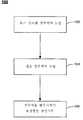
도 1은 본 발명의 구체예에 따른 유전 증착의 단순 개요를 나타내는 플로우챠트이다.1 is a flowchart showing a simple overview of dielectric deposition in accordance with an embodiment of the present invention.
도 2는 본 발명의 구체예에 따른 갭을 유전 재료로 충전시키는 방법을 예시하는 플로우챠트이다.2 is a flowchart illustrating a method of filling a gap with a dielectric material in accordance with an embodiment of the present invention.
도 3은 본 발명의 구체예에 따른 기판 상의 갭 내에 유전 재료를 증착시키고 어닐링하는 단계를 나타내는 플로우챠트이다.3 is a flowchart illustrating depositing and annealing a dielectric material in a gap on a substrate in accordance with an embodiment of the present invention.
도 4는 본 발명의 구체예에 따른 다층 실리콘 옥사이드 필름을 제조하는 방 법을 예시하는 플로우챠트이다.4 is a flowchart illustrating a method of making a multilayer silicon oxide film according to an embodiment of the invention.
도 5A 내지 도 5F는 본 발명의 구체예에 따른 다층 실리콘 옥사이드 필름으로 단계적으로 충전된 갭 구조를 지니는 기판을 나타낸다.5A-5F illustrate a substrate having a gap structure that is gradually filled with a multilayer silicon oxide film in accordance with embodiments of the present invention.
도 6A는 본 발명의 구체예에 따른 실리콘 옥사이드 층을 형성시키는데 사용될 수 있는 기판 가공 시스템의 수직 단면도를 나타낸다.6A shows a vertical cross sectional view of a substrate processing system that can be used to form a silicon oxide layer in accordance with an embodiment of the present invention.
도 6B는 본 발명의 구체예에 따른 기판 가공 시스템의 시스템 모니터/제어기 부품의 단순 설계도를 나타낸다.6B shows a simplified design of a system monitor / controller component of a substrate processing system in accordance with an embodiment of the present invention.
발명의 상세한 설명DETAILED DESCRIPTION OF THE INVENTION
기판의 표면 상에 및 갭 내에 유전 재료를 증착시키는 시스템 및 방법이 기재되어 있다. 유전 재료는 통상의 테트라에톡시실록산(tetraethoxysiloxane (TEOS)) 보다 낮은 탄소 원자 대 실리콘 원자 비율(C:Si 비율)을 지니는 유기-실리콘 화합물로부터 형성될 수 있다. 이들 화합물을 산소 전구체와 조합함으로써 형성되는 유전 필름은 전형적으로는 초기 증착된 TEOS 기재 실리콘 옥사이드 보다 낮은 탄소 함량, 낮은 다공도 및 낮은 WERRs를 지닌다. 이러한 구성은 필름이 TEOS 기재 옥사이드 필름에 비해서 균열, 공극 형성, 수분 흡수 및/또는 수축에 덜 민감하게 한다.Systems and methods are described for depositing a dielectric material on the surface of a substrate and in a gap. The dielectric material may be formed from an organo-silicon compound having a lower carbon atom to silicon atom ratio (C: Si ratio) than conventional tetraethoxysiloxane (TEOS). Dielectric films formed by combining these compounds with oxygen precursors typically have lower carbon content, lower porosity and lower WERRs than earlier deposited TEOS based silicon oxides. This configuration makes the film less susceptible to cracking, pore formation, moisture absorption and / or shrinkage than TEOS based oxide films.
유기-실리콘 화합물은 또한 TEOS O:Si 비율과 동일하거나 더 큰 산소 원자 대 실리콘 원자 비율(O:Si 비율)을 지닐 수 있다. 낮은 C:Si 비율 및 높은 O:Si 비율을 지니는 유기-실리콘 전구체는 실리콘 전구체로서 TEOS만을 사용하는 통상적으로 제조된 옥사이드에 비해서 더 낮은 탄소 함량을 지니는 더 높은 품질의 실리콘 옥사이드 필름을 생성시킨다. 구체예는 또한 분자 구조에 하나 이상의 Si-O-Si 연결을 지니는 유기-실리콘 전구체를 포함한다. Si 전구체 중의 이러한 연결은 탄소 및 히드록실기로부터의 오염이 감소된 SiOx 필름의 형성을 용이하게 한다.The organo-silicon compound may also have an oxygen atom to silicon atom ratio (O: Si ratio) equal to or greater than the TEOS O: Si ratio. Organic-silicon precursors with low C: Si ratios and high O: Si ratios produce higher quality silicon oxide films with lower carbon content compared to conventionally prepared oxides using only TEOS as the silicon precursor. Embodiments also include organo-silicon precursors having at least one Si—O—Si linkage to the molecular structure. This linkage in the Si precursors facilitates the formation of SiOx films with reduced contamination from carbon and hydroxyl groups.
유기-실리콘 화합물은 또한 Si-O기로 용이하게 산화될 수 있는 할로겐 및 질소 기를 포함하는 할로겐화된 실록산 및 실라족산을 포함할 수 있다. 할로겐화된 실록산은 염소화된 실록산, 예컨대, Si-C기가 분자 산소, 오존, 이산화질소, 과산화수소 등에 의해서 탄소 수준이 감소된 Si-O기로 용이하게 산화될 수 있는 옥타클로로트리실록산(octachlorotrisiloxane (OCTS))을 포함할 수 있다. 유사하게는, 실라족산, 예컨대, 헥사메톡시디실라족산(hexamethoxydisilazoxanes (HMDS-H))은 Si-O기로 용이하게 산화될 수 있는 Si-N기를 지닌다.The organo-silicon compound may also include halogenated siloxanes and silamic acids, including halogen and nitrogen groups, which can be readily oxidized to Si-O groups. Halogenated siloxanes are chlorinated siloxanes, such as octachlorotrisiloxane (OCTS), in which Si—C groups can be readily oxidized to Si—O groups with reduced carbon levels by molecular oxygen, ozone, nitrogen dioxide, hydrogen peroxide, and the like. It may include. Similarly, silamic acids, such as hexamethoxydisilazoxanes (HMDS-H), have Si-N groups that can be easily oxidized to Si-O groups.
유기-실리콘 화합물은 증착 챔버 중의 반응성 원자 산소 전구체에 도입되어, 증착된 유전 필름 중의 Si-O기의 형성을 더 증가시킬 수 있다. 원자 산소는, 증착 챔버로 보내져서 유기-실리콘 전구체와 반응되기 전에, 예를 들어, 원격 고밀도 플라즈마 생성 유닛을 사용함으로써 증착 챔버 외부에서 초기에 생성될 수 있다. 생성되는 실리콘 옥사이드 층은, 증착 챔버 내에서 유기-실리콘 전구체를 분자 산소, 오존 등과 반응시킴으로써 형성된 통상의 옥사이드 필름 보다 개선된 유동성 및 갭-흐름 특성 및 더 낮은 탄소 함량 및 다공성을 가질 수 있다. 본 발명의 방법, 생성물 및 시스템의 구체예에 대한 추가의 상세사항이 이하 기재될 것이다.The organo-silicon compound may be introduced into the reactive atomic oxygen precursor in the deposition chamber to further increase the formation of Si—O groups in the deposited dielectric film. Atomic oxygen may be initially generated outside the deposition chamber, for example by using a remote high density plasma generation unit, before being sent to the deposition chamber and reacted with the organo-silicon precursor. The resulting silicon oxide layer may have improved fluidity and gap-flow characteristics and lower carbon content and porosity than conventional oxide films formed by reacting an organo-silicon precursor in molecular deposition with oxygen, ozone and the like in the deposition chamber. Further details of embodiments of the methods, products, and systems of the present invention will be described below.
예시적인 유전 증착 방법Exemplary Dielectric Deposition Methods
도 1은 본 발명의 구체예에 따른 유전 증착의 단순 개요를 포함하는 플로우챠트를 나타낸다. 도시된 방법(100)은 유기-실리콘 전구체(102) 및 산소 전구체(104)를 증착 챔버에 도입하는 것을 포함한다. 전구체들은 챔버 내에서 반응하여 기판(106)의 표면 상에 및 갭 내에 유전층을 형성시킨다.1 shows a flowchart that includes a simple overview of dielectric deposition in accordance with an embodiment of the present invention. The illustrated
증착 챔버에 도입된 유기-실리콘 전구체는 8 미만의 C:Si 원자 비율(예, 7, 6, 5, 4, 3, 2, 또는 1 또는 그 미만의 C:Si 비율)을 지닐 수 있다. 이는 유기-실리콘 전구체 분자 내에서, 존재하는 각각의 실리콘 원자에 대해 8개 보다 적은 탄소 원자가 존재함을 의미한다. 비교해 보면, 이하 나타낸 테트라에톡시실록산(TEOS) 분자는 각각의 실리콘 원자에 대해 8개의 탄소 원자(즉, 8의 C:Si 비율)를 지닌다:The organo-silicon precursor introduced into the deposition chamber may have a C: Si atomic ratio of less than 8 (eg, a C: Si ratio of 7, 6, 5, 4, 3, 2, or 1 or less). This means that in the organo-silicon precursor molecule there are less than eight carbon atoms for each silicon atom present. In comparison, the tetraethoxysiloxane (TEOS) molecules shown below have 8 carbon atoms (ie, a C: Si ratio of 8) for each silicon atom:

유기-실리콘 전구체는 실록산 화합물, 예컨대, 다른 실록산 화합물 중에서도, 트리에톡시실록산(TRIES), 테트라메톡시실록산(TMOS), 트리메톡시실록산(TRIMOS), 헥사메톡시디실록산(HMODS), 옥타메톡시트리실록산(OMOTS), 및/또는 옥타메톡시도데카실록산(OMODDS)일 수 있다:The organo-silicon precursor may be a siloxane compound, such as triethoxysiloxane (TRIES), tetramethoxysiloxane (TMOS), trimethoxysiloxane (TRIMOS), hexamethoxydisiloxane (HMODS), octamethoxy, among other siloxane compounds. Trisiloxane (OMOTS), and / or octamethoxydodecasiloxane (OMODDS):

유기-실리콘 화합물은 또한 하나 이상의 질소기를 포함하는 실라족산 화합물일 수 있다. 실라족산 화합물은, 다른 실라족산 화합물 중에서도, 헥사메톡시디실라족산 (HMDS-H), 메틸 헥사메톡시디실라족산 (HMDS-CH3), 클로로헥사메톡시디실라족산 (HMDS-Cl), 헥사에톡시디실라족산(HEDS-H), 노나메톡시트리실라족산 (NMTS), 및 옥타메톡시시클릭실라족산 (OMCS)을 포함할 수 있다:The organo-silicon compound may also be a silamic acid compound comprising one or more nitrogen groups. The silamic acid compound is hexamethoxydisilanic acid (HMDS-H), methyl hexamethoxydisilamic acid (HMDS-CH3 ), chlorohexamethoxydisilamic acid (HMDS-Cl), and hexaethoxy, among other silaic acid compounds. Cidisilanic acid (HEDS-H), nonamethoxytrisilamic acid (NMTS), and octamethoxycyclic cyclic silamic acid (OMCS) may be included:

유기-실리콘 화합물은 추가로 하나 이상의 할로겐 기(예컨대, 플루오라이드, 클로라이드, 브로마이드, 또는 아이오다이드 기)를 포함하는 할로겐화된 실록산 화합물이다. 예를 들어, 할로겐화된 실록산은, 염소화된 실록산 화합물, 예컨대, 다른 염소화된 실록산 화합물 중에서도, 테트라클로로실란 (TECS), 디클로로디에톡시실록산 (DCDES), 클로로트리에톡시실록산(CTES), 헥사클로로디실록산 (HCDS), 및/또는 옥타클로로트리실록산 (OCTS)일 수 있다:Organo-silicon compounds are further halogenated siloxane compounds comprising one or more halogen groups (eg, fluoride, chloride, bromide, or iodide groups). For example, halogenated siloxanes include chlorinated siloxane compounds, such as tetrachlorosilane (TECS), dichlorodiethoxysiloxane (DCDES), chlorotriethoxysiloxane (CTES), hexachlorodioxy, among other chlorinated siloxane compounds. Siloxane (HCDS), and / or octachlorotrisiloxane (OCTS):

유기-실리콘 화합물은 또한 약 O, 0.5, 1, 2, 3, 4, 5, 6 등 또는 그 초과의 O:Si 비율을 지닐 수 있다. 예를 들어, TMOS는 4의 O:Si 원자 비율(TEOS와 동일)을 지닌다. 그 밖의 유기-실리콘 화합물, 예컨대, TRIES, 및 TRIMOS는 3의 O:Si 비율을 지닌다. 다른 화합물, 예컨대, HCDS는 0.5의 O:Si 비율을 지니며, TECS는 0의 O:Si 비율을 지닌다.The organo-silicon compound may also have an O: Si ratio of about 0, 0.5, 1, 2, 3, 4, 5, 6, or the like. For example, TMOS has an O: Si atomic ratio of 4 (equivalent to TEOS). Other organo-silicon compounds such as TRIES, and TRIMOS have an O: Si ratio of three. Other compounds, such as HCDS, have an O: Si ratio of 0.5 and TECS have an O: Si ratio of zero.
유기-실리콘 전구체는, 다른 유기-실리콘 화합물 중에서도, HMODS, OMOTS, OMODDS, HCDS, 및 OCTS에서 나타낸 바와 같이, Si-O-Si 연결을 추가로 포함할 수 있다. Si 전구체에서의 이러한 연결은 탄소 및 히드록실기로부터의 오염이 감소된 SiOx 필름의 형성을 촉진시킬 수 있다.The organo-silicon precursor may further comprise a Si—O—Si linkage, as shown in HMODS, OMOTS, OMODDS, HCDS, and OCTS, among other organo-silicon compounds. This linkage in the Si precursor can promote the formation of SiOx films with reduced contamination from carbon and hydroxyl groups.
유기-실리콘 전구체는 추가로, 다른 화합물 중에서도, 아미노실란, 예컨대, 트리실릴아민(TSA), 헥사메틸디실라잔 (HMDS), 실라트란, 테트라키스(디메틸아미노)실란, 비스(디에틸아미노)실란, 트리스(디메틸아미노)클로로실란, 및 메틸실라 트란을 포함할 수 있다:The organo-silicon precursors may further comprise aminosilanes, such as trisilylamine (TSA), hexamethyldisilazane (HMDS), silatran, tetrakis (dimethylamino) silane, bis (diethylamino), among other compounds. Silanes, tris (dimethylamino) chlorosilanes, and methylsilatran;

유기-실리콘 전구체는 또한 추가로 알콕시 디실란, 알콕시-알킬 디실란, 및 알콕시-아세톡시 디실란을 포함한 디실란을 포함할 수 있다. 알콕시 디실란은 하기 화합물을 포함할 수 있다:The organo-silicone precursor may further include disilanes, including alkoxy disilanes, alkoxy-alkyl disilanes, and alkoxy-acetoxy disilanes. Alkoxy disilanes may include the following compounds:

상기 식에서,Where
R1-6은 독립적으로 C1-3 알킬옥시기일 수 있다. 예를 들어, 알콕시 디실란은, 다른 알콕시 디실란 중에서도, 헥사메톡시디실란, 및 헥사에톡시디실란을 포함할 수 있다.R1 is independently a C1-6-3 may alkyloxy group. For example, the alkoxy disilane may include hexamethoxydisilane and hexaethoxydisilane, among other alkoxy disilanes.
알콕시 디실란은 또한 Si 부분에 결합된 알콕시기를 지닌 시클릭 디실란 화합물을 포함할 수 있다. 예를 들어, 알콕시시클로실란은, 다른 것들 중에서도, 옥타에톡시시클로부타실란, 데카부타옥시시클로펜타실란, 및 도데카메톡시시클로헥사실란을 포함할 수 있다. 알콕시 디실란의 일부예는 하기된 바와 같다:Alkoxy disilanes may also include cyclic disilane compounds having an alkoxy group bonded to the Si moiety. For example, the alkoxycyclosilane may include octaethoxycyclobutasilane, decabutaoxycyclopentasilane, and dodecamethoxycyclohexasilane, among others. Some examples of alkoxy disilanes are as follows:

알콕시-알킬 디실란은 하기 화합물을 포함할 수 있다:Alkoxy-alkyl disilanes may include the following compounds:

상기 식에서, R7-12는 독립적으로 C1-3 알킬기 또는 C1-3 알킬옥시기일 수 있으며, R7-12중 하나 이상은 알킬기이고, R7-12중 하나 이상은 알킬옥시기이다. 알콕시-알킬 디실란은 또한 알킬 및 알콕시 부분을 지닌 시클릭 디실란, 예컨대, 결합된 하나 이상의 알킬 및 알콕시를 지니는 부타실란, 펜타실란, 헥사실란, 헵타실란, 옥타실란 등을 포함할 수 있다. 그러한 예에는, 다른 알콕시-알킬 시클로실란 중에서도, 옥타메틸-1,4-디옥사-2,3,5,6-테트라실라시클로헥산; 1,4-디옥사-2,3,5,6-테트라실라시클로헥산; 및 1,2,3,4,5,6-헥사메톡시-1,2,3,4,5,6-헥사메틸시클로헥사실란을 포함한다. 알콕시-알킬 디실란의 일부 예는 다음과 같다:Wherein R7-12 may independently be a C1-3 alkyl group or a C1-3 alkyloxy group, at least one of R7-12 is an alkyl group, and at least one of R7-12 is an alkyloxy group. Alkoxy-alkyl disilanes may also include cyclic disilanes having alkyl and alkoxy moieties, such as butasilane, pentasilane, hexasilane, heptasilane, octasilane, and the like having one or more alkyl and alkoxy bounds. Such examples include octamethyl-1,4-dioxa-2,3,5,6-tetrasilacyclohexane, among other alkoxy-alkyl cyclosilanes; 1,4-dioxa-2,3,5,6-tetrasilacyclohexane; And 1,2,3,4,5,6-hexamethoxy-1,2,3,4,5,6-hexamethylcyclohexasilane. Some examples of alkoxy-alkyl disilanes are as follows:

알콕시-아세톡시 디실란은 하기 화합물을 포함할 수 있다:Alkoxy-acetoxy disilanes may include the following compounds:

상기 식에서, R13-17은 독립적으로 C1-3 알킬기, C1-3알콕시기 또는 아세톡시기일 수 있으며, R13-17중 하나 이상은 알콕시기이고, R13-17중 하나 이상은 아세톡시기이다.Wherein R13-17 can be independently a C1-3 alkyl group, a C1-3 alkoxy group or an acetoxy group, at least one of R13-17 is an alkoxy group and at least one of R13-17 is ace It is a oxy group.
유기-실리콘 전구체는 또한 추가로 유기시클로실란, 예컨대, 시클로부타실란, 시클로펜타실란, 시클로헥사실란, 시클로헵타실란, 시클로옥타실란 등을 포함 할 수 있다.The organo-silicon precursor may also further include organocyclosilanes such as cyclobutasilane, cyclopentasilane, cyclohexasilane, cycloheptasilane, cyclooctasilane, and the like.
산소 전구체는 분자 산소(O2), 오존(O3), 질소-산소 화합물(예컨대, NO, NO2, N2O 등), 수소-산소 화합물(예컨대, H2O, H2O2 등), 및 그 밖의 산소 함유 전구체 및 이들 전구체의 조합물을 포함할 수 있다. 일부 구체예에서, 산소 전구체는 원격적으로 생산되고 유기-실리콘 전구체와 함께 증착 챔버 내로 도입되는 원자 산소 라디칼을 포함할 수 있다.Oxygen precursors include molecular oxygen (O2 ), ozone (O3 ), nitrogen-oxygen compounds (eg NO, NO2 , N2 O, etc.), hydrogen-oxygen compounds (eg H2 O, H2 O2, etc. ), And other oxygen containing precursors and combinations of these precursors. In some embodiments, the oxygen precursor may include atomic oxygen radicals that are produced remotely and introduced into the deposition chamber along with the organo-silicon precursor.
이제 도 2를 참조하면, 본 발명의 구체예에 따른 유전 재료로 갭을 충전시키는 방법(200)을 예시하는 플로우챠트가 도시되어 있다. 방법(200)은 기판을 증착 챔버에 제공하고, 이어서 유기-실리콘 전구체(202) 및 산소 전구체(204)를 챔버에 도입하는 것을 포함할 수 있다. 기판은 반도체 웨이퍼(예컨대, 200mm, 300mm, 400mm 등의 실리콘 웨이퍼)일 수 있으며, 이전의 공정에서 형성된 구조물, 디바이스 성분 등을 포함할 수 있다. 예를 들어, 기판은 높은 높이 대 폭 종횡비(aspect raio)(예컨대, 5:1 또는 그 초과, 6:1 또는 그 초과, 7:1 또는 그 초과, 8:1 또는 그 초과, 9:1 또는 그 초과, 10:1 또는 그 초과, 11:1 또는 그 초과, 12:1 또는 그 초과 등)를 갖는 갭, 트렌치 등을 포함할 수 있다. 유전 재료는 기판의 갭 내 및 다른 표면에 증착된다.Referring now to FIG. 2, a flowchart illustrating a
상기 주지된 바와 같이, 유기-실리콘 전구체는 실록산, 할로겐화된 실록산, 및/또는 실라족산 화합물을 포함할 수 있으며, 8 미만의 C:Si 원자 비율의 유기-실리콘 화합물을 포함할 수 있다. 실리콘 전구체는 증착 챔버에 도입 전에 또는 도입 동안에 캐리어 가스와 혼합될 수 있다. 캐리어 가스는 기판 상의 옥사이드 필름의 형성을 과도하게 방해하지 않는 불활성 가스일 수 있다. 캐리어 가스의 예는, 다른 가스 중에서도, 헬륨, 네온, 아르곤, 및 수소(H2)를 포함한다.As noted above, the organo-silicon precursor may comprise siloxanes, halogenated siloxanes, and / or silamic acid compounds, and may comprise organo-silicon compounds with a C: Si atomic ratio of less than eight. The silicon precursor may be mixed with the carrier gas prior to or during introduction into the deposition chamber. The carrier gas may be an inert gas that does not excessively interfere with the formation of an oxide film on the substrate. Examples of the carrier gas include helium, neon, argon, and hydrogen (H2 ), among other gases.
예를 들어, 유기-실리콘 전구체는 유기-실리콘 화합물(가스 또는 액체)을 헬륨과 혼합함으로써 약 600 내지 약 2400 sccm의 유량으로 실온 유기-실리콘 전구체를 통해서 증착 챔버에 도입되어 챔버에 약 800 내지 약 1600mgm 속도의 전구체 흐름을 제공할 수 있다.For example, the organo-silicon precursor is introduced into the deposition chamber through the room temperature organo-silicon precursor at a flow rate of about 600 to about 2400 sccm by mixing the organo-silicon compound (gas or liquid) with helium, thereby bringing about 800 to about It can provide precursor flow at 1600 mgm.
산소 전구체는 분자 산소(O2), 오존(O3), 질소-산소 화합물(예컨대, NO, NO2, N2O 등), 수소-산소 화합물(예컨대, H2O, H2O2 등), 탄소-산소 화합물(예컨대, CO, CO2 등), 및 다른 산소 함유 전구체 및 이러한 전구체의 조합을 포함할 수 있다. 방법(300)에 대해서 이하 상세히 기재된 바와 같이, 산소 전구체는 또한 원격적으로 생산되고 유기-실리콘 전구체와 함께 증착 챔버 내로 도입되는 원자 산소 라디칼을 포함할 수 있다.Oxygen precursors include molecular oxygen (O2 ), ozone (O3 ), nitrogen-oxygen compounds (eg NO, NO2 , N2 O, etc.), hydrogen-oxygen compounds (eg H2 O, H2 O2, etc. ), Carbon-oxygen compounds (eg, CO, CO2, etc.), and other oxygen containing precursors and combinations of such precursors. As described in detail below for the
방법(200)은 전구체로부터 증착 챔버 내에서 플라즈마를 생성시키고, 유전 재료(206)의 제 1 부분을 형성시키는 것을 포함한다. 방법(200)의 구체예에서, 산소 및 유기-실리콘 전구체는 증착 챔버에 도입되기 전에 혼합되지 않는다. 전구체는 반응 챔버 둘레에 분포된 공간적으로 분리된 전구체 유입구를 통해서 챔버에 유입될 수 있다. 예를 들어, 산소 전구체는 챔버의 상부에 있는 유입구(또는 유입구들)로부터 유입될 수 있으며, 기판 위에 직접적으로 정위될 수 있다. 유입구는 산소 전구체의 흐름을 기판 증착 표면에 수직인 방향으로 유도한다. 한편, 실리콘 전구체가 증착 챔버 측면 둘레에 있는 하나 이상의 유입구로부터 유입될 수 있다. 유입구는 실리콘 전구체의 흐름을 증착 표면에 대체로 평행한 방향으로 유도할 수 있다.The
산소와 유기-실리콘 플라즈마가 증착 챔버 내에서 반응함에 따라서, 이는 기판 증착 표면 상의 실리콘 옥사이드 유전층의 제 1 부분을 형성한다. 초기 옥사이드 층은 우수한 유동성을 지니며, 증착 표면에 존재하는 구조물 내의 갭, 트렌치, 공극, 시임(seam) 등으로 신속하게 이동할 수 있다. 이는 방법(200)이 높은 높이 대 폭 종횡비(예컨대, 약 5:1, 6:1, 7:1, 8:1, 9:1, 10:1, 11:1, 및 12:1 또는 그 초과의 종횡비(ARs))를 지니는 갭, 트렌치, 및 그 밖의 표면 구조물 내의 공극 및 시임이 실질적으로 없는 옥사이드 충전을 제공하게 한다.As oxygen and the organo-silicon plasma react in the deposition chamber, this forms the first portion of the silicon oxide dielectric layer on the substrate deposition surface. The initial oxide layer has good flowability and can quickly move to gaps, trenches, voids, seams, etc. within the structure present at the deposition surface. This means that the
유전 재료의 제 1 부분이 형성된 후에, 챔버 내로의 전구체의 흐름은 중단될 수 있고, 재료는 에칭(208)될 수 있다. 에칭 단계는 재료 중의 불순물을 해리시키고 제거하는데 이용될 수 있으며, 또한 재료를 평탄화시키는데 이용될 수 있다. 에칭 공정은 단일-스텝 에치(single-step etch), 또는 멀티스텝 에치를 포함할 수 있다. 멀티스텝 에치 공정은 저-밀도 플라즈마를 이용하여 더 큰 유기분자를 해리시키고 유전 재료 중의 탄소의 적어도 일부를 제거하는 제 1 에치를 포함할 수 있다. 이러한 저-밀도 플라즈마 에치는 RPS 시스템을 사용하여 옥사이드 층을 에칭하는 Ar/O2 플라즈마를 생성시키는 것을 포함할 수 있다. 에칭 조건은, 예를 들어, 약 5500 와트의 전력에서 1600 sccm O2 및 400 sccm 아르곤의 흐름으로부터의 플라즈마를 스트라이킹(striking)하고, 이를 약 760mTorr의 압력에서 증착 챔버에 도입하는 것을 포함할 수 있다. 이러한 플라즈마 에치는 옥사이드 층으로부터 탄소 불순물을 제거하고 더 큰 탄소 기를 해리시킬 수 있다.After the first portion of the dielectric material is formed, the flow of the precursor into the chamber can be stopped and the material can be etched 208. The etching step can be used to dissociate and remove impurities in the material, and can also be used to planarize the material. The etching process may include single-step etch, or multistep etch. The multistep etch process may comprise a first etch using a low-density plasma to dissociate larger organic molecules and remove at least some of the carbon in the dielectric material. Such low-density plasma etch can include generating an Ar / O2 plasma that etches the oxide layer using an RPS system. Etching conditions may include, for example, striking plasma from a flow of 1600 sccm O2 and 400 sccm argon at a power of about 5500 watts and introducing it into the deposition chamber at a pressure of about 760 mTorr. . Such plasma etch can remove carbon impurities from the oxide layer and dissociate larger carbon groups.
이러한 에치 후에, 옥사이드 층의 제 2 에치가 더 높은 플라즈마 밀도에서 수행되어 층 중의 히드록실기의 적어도 일부를 제거할 수 있다. 이러한 더 높은 밀도 플라즈마 에치는 고전력 RF 장(high-power RF field)(예컨대, 6000와트)에 의한 분자 산소의 흐름(예컨대, 600sccm)의 해리로부터 형성된 플라즈마에 층을 노출시키는 것을 포함할 수 있다. 산소 플라즈마는, 예를 들어, 8mTorr의 압력에서 증착 챔버에 도입될 수 있으며, 옥사이드 층 내의 -OH 기와 반응하여 실리콘 디옥사이드 및 물을 형성시킬 수 있다.After such etch, a second etch of the oxide layer may be performed at a higher plasma density to remove at least some of the hydroxyl groups in the layer. Such higher density plasma etch may include exposing a layer to a plasma formed from dissociation of a flow of molecular oxygen (eg, 600 sccm) by a high-power RF field (eg, 6000 watts). The oxygen plasma can be introduced to the deposition chamber at a pressure of 8 mTorr, for example, and can react with —OH groups in the oxide layer to form silicon dioxide and water.
제 1 층의 에칭 후에, 전구체가 증착 챔버에 재도입되고, 반응하여 기판(210)의 갭 내 및 다른 표면에 유전 재료의 제 2 부분을 형성시킨다. 제 2 부분은 또한 제 1 층과 동일한 반응 조건하에 형성되는 옥사이드 층일 수 있거나, 상이한 조건(예컨대, 챔버 압력, 온도, 유기-실리콘 전구체 등)하에 형성될 수 있다.After etching the first layer, the precursor is reintroduced into the deposition chamber and reacted to form a second portion of the dielectric material in the gap and on the other surface of the
제 2 층이 형성된 후에, 이는 또한 에칭되어 불순물 수준을 감소시키고/거나 층을 평탄화시킬 수 있다. 제 2 층은 제 1 층을 에칭시키는데 이용된 공정과 동일한 공정을 이용해 에칭될 수 있거나, 상이한 공정(예컨대, 상이한 수의 에칭 단계, 상이한 에치 전구체, 상이한 전력 수준 등)을 이용해 에칭될 수 있다.After the second layer is formed, it can also be etched to reduce the impurity level and / or to planarize the layer. The second layer may be etched using the same process used to etch the first layer, or may be etched using different processes (eg, different numbers of etching steps, different etch precursors, different power levels, etc.).
유전 재료의 제 1 부분 및 제 2 부분 (및 증착될 수 있는 임의의 후속된 부분)의 형성 및 처리 후에, 재료는 어닐링(212)되어 균일한 고품질의 실리콘 옥사이드 갭충전(gapfill)을 형성시킬 수 있다. 최종 갭충전은 3.0 미만의 유전상수(즉, k-값) 및 2:1 미만(예컨대, 약 1.8:1 내지 약 1.4:1)의 습식-에치 속도 비(WERR)를 지닐 수 있다. 갭충전은 충전 부피 전체에 걸쳐서 균일하고, 만약에 있다면, 근소한 공극 또는 시임을 함유할 수 있다.After formation and processing of the first and second portions of the dielectric material (and any subsequent portions that may be deposited), the material may be annealed 212 to form a uniform high quality silicon oxide gapfill. have. The final gapfill may have a dielectric constant of less than 3.0 (ie, a k-value) and a wet-etch rate ratio (WERR) of less than 2: 1 (eg, about 1.8: 1 to about 1.4: 1). Gap filling is uniform throughout the fill volume and may contain minor voids or seams, if any.
도 3은 본 발명의 추가의 구체예에 따른 기판 상의 갭 내에 유전 재료를 증착하고 어닐링하는 단계를 나타내는 플로우챠트이다. 방법(300)은 유기-실리콘 전구체를 증착 챔버(302)에 도입하는 것을 포함한다. 방법(300)은 또한 산소 함유 전구체, 예컨대, 분자 산소(O2), 오존(O3), 질소-산소 화합물(예컨대, NO, NO2, N2O 등), 수소-산소 화합물(예컨대, H2O, H2O2 등), 탄소-산소 화합물(예컨대, CO, CO2 등), 및 그 밖의 산소 함유 전구체 및 그러한 전구체들의 조합물의 해리에 의해서 고도의 반응성 원자 산소 전구체(304)를 생성시키는 것을 포함한다.3 is a flowchart illustrating depositing and annealing a dielectric material in a gap on a substrate in accordance with a further embodiment of the present invention. The
산소 함유 전구체는 원격적으로 해리되어 원자 산소를 생성시킬 수 있다. 해리 공정은, 다른 방법 중에서도, 열적 해리, 자외선 해리, 및/또는 플라즈마 해리를 포함할 수 있다. 플라즈마 해리는 원격 플라즈마 생성 챔버 내에서 헬륨, 아르곤 등으로부터의 플라즈마를 스트라이킹하고, 산소 전구체를 플라즈마에 도입하여 원자 산소 전구체를 생성시키는 것을 포함할 수 있다. 예를 들어, 원자 산소는, 예를 들어, 약 600 내지 1200 sccm으로 흐르는 분자 산소(O2)와, 예를 들어, 약 900 내지 1800 sccm으로 흐르는 아르곤 가스가 조합된 가스 스트림에 4000 내지 6000와트(예컨대, 5500와트)의 RF 전력을 공급하는 원격 고-밀도 플라즈마 생성기에서 생성될 수 있다.The oxygen containing precursor can be dissociated remotely to produce atomic oxygen. The dissociation process may include thermal dissociation, ultraviolet dissociation, and / or plasma dissociation, among other methods. Plasma dissociation may include striking plasma from helium, argon, etc. in a remote plasma generation chamber, and introducing an oxygen precursor into the plasma to produce an atomic oxygen precursor. For example, atomic oxygen is 4000 to 6000 watts in a gas stream combining, for example, molecular oxygen (O2 ) flowing at about 600 to 1200 sccm and argon gas flowing at, for example, about 900 to 1800 sccm. (Eg, 5500 watts) in a remote high-density plasma generator that supplies RF power.
반응성 원자 산소 플라즈마는 이어서 증착 챔버(306)에 도입되고, 여기서, 그러한 반응성 원자 산소 플라즈마는 챔버로 또한 도입되는 유기-실리콘 전구체와 처음으로 혼합될 수 있다. 높은 반응성 원자 산소는 중간의 온도(예컨대, 100℃미만의 반응 온도) 및 압력(예컨대, 0.5 내지 6 Torr의 전체 챔버 압력)에서 실리콘 전구체(308)(및 반응 챔버 내에 존재할 수 있는 다른 증착 전구체)와 반응할 것이다.The reactive atomic oxygen plasma is then introduced to the
구체예는 다중-포트 샤워헤드(multi-port showerhead)의 각각의 포트를 통해서 원자 산소 및 실리콘 전구체를 전달하는 것을 포함한다. 예를 들어, 기판 위에 위치된 샤워헤드는 전구체가 증착 챔버에 유입되게 하는 패턴의 구멍들을 포함할 수 있다. 하나의 서브세트(subset) 구멍들에는 원자 산소 전구체가 공급될 수 있으며, 두 번째 서브세트 구멍들에는 실리콘 전구체가 공급된다. 상이한 세트의 구멍들을 통해서 이동하는 전구체는 증착 챔버내로 빠져나갈 때까지 서로 유체적으로 분리될 수 있다. 전구체 취급 장치의 형태 및 디자인에 대한 추가의 상세한 사항은 발명의 명칭이 "유전 갭충전을 위한 공정 챔버(PROCESS CHAMBER FOR DIELECTRIC GAPFILL)"인 2006년 5월 30일자 출원된 루보미르스키(Lubomirsky) 등에게 공동 양도된 미국가특허출원 제60/803,499호에 기재되어 있으며, 본원에서는 모든 목적을 위하여 상기 특허출원의 전체 내용이 참조로 통합된다.Embodiments include delivering atomic oxygen and silicon precursor through each port of a multi-port showerhead. For example, the showerhead located above the substrate may include holes in the pattern that allow precursors to enter the deposition chamber. One subset holes may be supplied with an atomic oxygen precursor, and the second subset holes may be supplied with a silicon precursor. Precursors moving through different sets of holes may be fluidically separated from one another until they exit into the deposition chamber. Further details on the form and design of the precursor handling device are described in Lubomirsky, filed May 30, 2006, entitled PROCESS CHAMBER FOR DIELECTRIC GAPFILL. United States Patent Application No. 60 / 803,499, which is commonly assigned, is hereby incorporated by reference in its entirety for all purposes.
전구체가 챔버 내에서 서로 반응함에 따라서, 유전층이 기판(310) 상에 증착된다. 증착 동안의 챔버 내의 전체 압력은, 예를 들어, 약 0.5 Torr 내지 약 6 Torr일 수 있다. 더 높은 전체 압력(예컨대, 1.3 Torr)은 더욱 유동형 품질의 옥사이드 필름을 증착시킬 수 있지만, 더 낮은 압력(예컨대, 0.5 Torr)은 더욱 정각의 옥사이드 층(conformal oxide layer)을 증착시킬 수 있다. 반응 챔버 내의 증착 온도는 비교적 낮을 수 있다(예컨대, 100℃ 또는 그 미만). 증착 속도는 약 500Å/분 내지 약 3000Å/분(예컨대, 1500Å/분)의 범위일 수 있다. 층의 두께는 약 50Å 내지 약 500Å(예컨대, 약 100Å 내지 약 200Å)일 수 있다.As the precursors react with each other in the chamber, a dielectric layer is deposited on the
유전층의 증착 후에, 수분의 일부를 제거하고 층의 경도를 증가시키는 제 1 어닐링(312)이 수행될 수 있다. 이러한 초기 어닐링 단계는 불활성 환경(예컨대, 건조한-N2 환경)에서 약 1 분 내지 10분 동안 옥사이드 층을 가열하는 것을 포함할 수 있다. 기판 구조물에 형성된 금속 라인을 손상시키지 않을 열적 어닐링 온도가 선택될 수 있으며, 예컨대, 옥사이드 층이 알루미늄 금속 라인 상에 증착되는 금속간 유전체인 경우에 그러하다.After deposition of the dielectric layer, a
대안적으로(또는 추가로), 제 1 어닐링 단계는 약 1 분 내지 약 30분 동안 자외선(UV) 광에 실리콘 옥사이드 층을 노출시키는 것을 포함할 수 있다. 열적 어닐링과 유사하게, UV 어닐링이 초기에 증착된 옥사이드 필름 중에 존재하는 수분 중 일부를 제거하고, 또한 필름의 경도를 증가시킬 수 있다.Alternatively (or in addition), the first annealing step may include exposing the silicon oxide layer to ultraviolet (UV) light for about 1 minute to about 30 minutes. Similar to thermal annealing, UV annealing can remove some of the moisture present in the initially deposited oxide film and also increase the hardness of the film.
제 1 어닐링의 종료 후에, 제 2 어닐링 단계(314)가 수행되어 옥사이드 층으로부터 수분과 실라놀 결합을 추가로 제거할 수 있다. 이러한 어닐링 단계(314)에서, 실질적으로 모든 수분과 실라놀이 제거되어, 초기에 증착된 옥사이드에 비해서 또는 제 1 어닐링 단계에서 층이 처리된 후에 비해서 층이 더 낮은 k-값 및 더 낮은 WERR 값을 지니게 할 수 있다. 이러한 제 2 어닐링은 유전체 옥사이드로부터 물과 실라놀기를 제거하는데 효율적인 플라즈마에 옥사이드 층을 노출시키는 것을 포함할 수 있다. 그러나, 제 1 어닐링 후에, 옥사이드 층은 충분한 경도를 지녀서 플라즈마가 옥사이드에 존재하는 탄소기를 파괴하는 것을 감소(또는 방지)시킨다. 따라서, 낮은-k의 탄소 함유 옥사이드 층에 대해서, 플라즈마 어닐링은 층의 k-값을 현저하게 상승시키기 위해 충분한 탄소를 제거하지 않는다.After the end of the first annealing, a
이제 도 4를 참조하면, 본 발명의 구체예에 따른 다층 실리콘 옥사이드 필름을 제조하는 방법(400)을 예시하는 또 다른 플로우챠트가 나타나 있다. 방법(400)은 기판을 증착 챔버(402)에 제공하고, 전구체(예컨대, 원자 산소 및 유기-실리콘 전구체)를 챔버(404)에 도입하는 것을 포함한다. 전구체는 반응하여 기판(406) 상에 실리콘 옥사이드 층을 형성하고, 이어서, 옥사이드 층이 에칭(408)될 수 있다.Referring now to FIG. 4, another flow chart illustrating a method 400 of making a multilayer silicon oxide film in accordance with an embodiment of the present invention is shown. The method 400 includes providing a substrate to the
이때, 증착된 옥사이드 층의 누적 두께가 예정점(410)에 도달했는지를 측정하는 검사가 수행될 수 있다. 전체 옥사이드 필름의 예정 두께 수준이 도달되면, 증착 및 에칭 사이클이 종료될 수 있으며, 필름이 어닐링(412)될 수 있다. 그러나, 두께 수준이 부합되지 않으면, 또 다른 옥사이드 증착 및 에칭 사이클이 수행되어 옥사이드 필름에 적어도 또 하나의 추가의 층을 추가할 수 있다.At this time, a test may be performed to determine whether the cumulative thickness of the deposited oxide layer has reached a
옥사이드 필름이 소정의 두께에 도달했는지를 측정하는 것은 증착되고 에칭된 층의 두께 측정에 의해서 수행될 수 있거나, 요구되는 필름 두께에 도달하는데 요구되는 층의 수를 계산함으로써 수행될 수 있다. 예를 들어, 각각의 증착되고 에칭된 층이 100 Å 두께이고, 요구되는 필름 두께가 1.2㎛인 경우, 필름을 형성시키기 위하여 12회의 증착 및 에칭 사이클이 수행되어야 한다. 각각의 증착된 층의 두께는 옥사이드 증착 속도에 영향을 주는 파라메터, 예컨대, 다른 파라메터 중에서도, 반응성 전구체의 형태 및 유량, 증착 챔버 내의 전체 압력, 및 온도를 조절함으로써 설정될 수 있다. 상기 주지된 바와 같이, 옥사이드 층의 전형적인 증착 속도는 약 500Å/분 내지 약 3000Å/분(예컨대, 약 1500Å/분)이다.Determining whether the oxide film has reached a predetermined thickness may be performed by measuring the thickness of the deposited and etched layer, or by calculating the number of layers required to reach the required film thickness. For example, if each deposited and etched layer is 100 mm 3 thick and the required film thickness is 1.2 μm, 12 deposition and etching cycles must be performed to form the film. The thickness of each deposited layer can be set by adjusting the shape and flow rate of the reactive precursor, the overall pressure in the deposition chamber, and the temperature, among other parameters that affect the oxide deposition rate. As noted above, typical deposition rates of oxide layers are from about 500 kPa / min to about 3000 kPa / min (eg, about 1500 kPa / min).
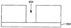
도 5A 내지 도 5F는 다수 사이클 증착-에치 옥사이드 층 형성 과정의 구체예를 사용함으로써 다층 실리콘 옥사이드 필름으로 단계적으로 충전되는 갭 구조물을 지니는 기판을 나타내고 있다. 도 5A는 갭(504)이 그 위에 형성되는 기판(502)을 나타내고 있다. 도 5A 내지 도 5F에 나타낸 갭(504)이 상대적으로 낮은 종횡비로 작도되어 옥사이드 충전 층의 성장을 더욱 명확히 나타내고 있음을 인지할 수 있을 것이다. 본 갭충전 방법의 구체예는 5:1, 6:1, 7:1, 8:1, 9:1, 10:1, 11:1, 12:1, 13:1, 14:1, 및 15:1 또는 그 초과의 종횡비를 지니는 갭으로의 공극 및 시임 없는 증착을 포함할 수 있다.5A-5F illustrate a substrate having a gap structure that is stepped into a multilayer silicon oxide film by using an embodiment of a multicycle deposition-etch oxide layer formation process. 5A shows a
도 5B는 갭(504) 내에 증착된 제 1 옥사이드 층(506a)을 나타내고 있다. 층을 형성한 실리콘 옥사이드는 양호한 유동성 품질을 지녀서 필름이 갭(504)의 바닥으로 신속히 이동하게 한다. 따라서, 갭(504)의 바닥에 증착된 옥사이드의 두께는 갭의 측벽을 따른(along) 옥사이드 두께 보다 클 수 있다.5B shows the
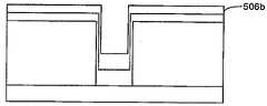
도 5C 및 도 5D는 갭(504) 내에 앞서 증착되고 에칭된 층상에 증착되는 추가의 옥사이드 층(506b, 506c 등)을 나타내고 있다. 이들 추가의 층은, 요구되는 옥사이드 필름 두께 수준이 도달될 때까지(예컨대, 갭(504)의 상부), 갭(504)내에서 바닥으로부터 상향으로 형성될 수 있다.5C and 5D show
다수의 옥사이드 층 중의 마지막 층이 증착되고 에칭되면, 도 5E에 도시된 바와 같이, 어닐링이 수행되어 층을 균일한 필름(508)으로 형성시킬 수 있다. 필름은, 예를 들어, 플라즈마 에칭 또는 CMP에 의해서 평탄화되어서 갭(504)의 상부 상에 형성된 증착 재료를 제거할 수 있다. 도 5F는 만약에 있다면, 근소한 공극 또는 시임을 지니며 높은 필름-품질 및 유전 특성을 지니는 나머지 실리콘 옥사이드 갭충전(510)을 나타낸다.Once the last of the plurality of oxide layers is deposited and etched, annealing may be performed to form the layer into a
예시적인 기판 가공 시스템Example Substrate Processing System
본 발명의 구체예를 실행할 수 있는 증착 시스템은, 다른 시스템 유형들 중에서도, 고밀도 플라즈마 화학적 기상 증착(high-density plasma chemical vapor deposition (HDP-CVD)) 시스템, 플라즈마 향상된 화학적 기상 증착(plasma enhanced chemical vapor deposition (PECVD)) 시스템, 감압하 화학적 기상 증착(sub-atmospheric chemical vapor deposition (SACVD)) 시스템, 및 열화학적 기상 증착 시스템을 포함할 수 있다. 본 발명의 구체예를 실행할 수 있는 CVD 시스템의 특정의 예는 미국 캘리포니아 산타 클라라 소재의 어플라이드 머티리얼스, 인코포레이티드로부터 구매할 수 있는 CENTURA ULTIMA™ HDP-CVD 챔버/시스템 및 PRODUCER™ PECVD 챔버/시스템을 포함한다.Deposition systems that may implement embodiments of the invention include, among other system types, high-density plasma chemical vapor deposition (HDP-CVD) systems, plasma enhanced chemical vapor deposition. deposition (PECVD) systems, sub-atmospheric chemical vapor deposition (SACVD) systems, and thermochemical vapor deposition systems. Specific examples of CVD systems that may implement embodiments of the present invention are CENTURA ULTIMA ™ HDP-CVD chambers / systems and PRODUCER ™ PECVD chambers / systems available from Applied Materials, Inc., Santa Clara, CA. It includes.
본 발명의 예시적인 방법과 함께 사용될 수 있는 기판 가공 시스템의 예는 발명의 명칭이 "유전 갭충전을 위한 공정 챔버(PROCESS CHAMBER FOR DIELECTRIC GAPFILL)"인 2006년 5월 30일자 출원된 루보미르스키 등에 공동 양도된 미국가특허출원 제60/803,499에 도시되고 설명된 것들을 포함할 수 있으며, 본원에서는 모든 목적을 위하여 상기 특허출원의 전체 내용이 참조로 통합된다. 추가의 예시적인 시스템은 미국특허 제6,387,207호 및 제6,830,624호에 도시되고 설명된 것들을 포함할 수 있으며, 본원에서는 모든 목적을 위하여 상기 특허가 또한 참조로 통합된다.Examples of substrate processing systems that can be used with the exemplary methods of the present invention include Lubomirsky et al., Filed May 30, 2006, entitled PROCESS CHAMBER FOR DIELECTRIC GAPFILL. Co-assigned US patents may include those shown and described in
이제 도 6A를 참조하면, 챔버벽(15a) 및 챔버 리드 어셈블리(chamber lid assembly: 15b)를 포함하는 진공 또는 가공 챔버(15)를 지닌 CVD 시스템(10)의 수직 단면도가 나타나 있다. CVD 시스템(10)은 가공 챔버(15) 내 중심에 있는 가열된 페데스탈(pedestal: 12) 상에 놓여 있는 기판(도시되지 않음)에 공정 가스를 분산시키는 가스 분배 매니폴드(11)를 함유한다. 가스 분배 매니폴드(11)는 용량 플라즈마(capacitive plasma)를 형성시키는 전극으로서 작용하게 하기 위해서 전기 전도성 재료로부터 형성될 수 있다. 가공 동안, 기판(예컨대, 반도체 웨이퍼)은 페데스탈(12)의 평탄(또는 약간 볼록) 표면(12a) 상에 정위된다. 페데스탈(12)은 매니폴드(11)에 아주 인접되는 상부 공정 위치(도 6A에서 점선(14)으로 표시됨)와 하부 로딩/오프-로딩 위치(도 6A에 도시됨) 사이를 조절가능하게 움직일 수 있다. 센터보드(도시되지 않음)는 웨이퍼의 위치에 대한 정보를 제공하는 센서를 포함한다.Referring now to FIG. 6A, a vertical cross-sectional view of a
증착 및 캐리어 가스는 통상의 평탄한 환형 가스 분배 페이스플레이트(faceplate: 13a)의 천공 홀(13b)을 통해서 챔버(15) 내로 도입된다. 더욱 특히, 증착 공정 가스는 유입 매니폴드(11)를 통해서, 통상의 천공된 블록커 플레이트(blocker plate)를 통해서, 및 이어서 가스 분배 페이스플레이트(13a) 내의 홀(hole: 13b)을 통해서 챔버 내로 흐른다.The deposition and carrier gas are introduced into the chamber 15 through the puncture holes 13b of a conventional flat annular gas distribution faceplate 13a. More particularly, the deposition process gas enters the chamber through the
매니폴드(11)에 도달하기 전에, 증착 및 캐리어 가스는 가스 공급 라인을 통해서 가스 공급원으로부터 혼합 시스템으로 유입되며, 그러한 혼합 시스템에서, 이들은 혼합되고 매니폴드(11)에 이송된다. 일반적으로, 각각의 공정 가스를 위한 공급 라인은 (i) 챔버 내로의 공정 가스의 흐름을 자동적으로 또는 수동적으로 차단하는데 이용될 수 있는 수 개의 안전 차단 밸브(도시되지 않음) 및 (ii) 공급 라인을 통한 가스 흐름을 측정하는 매스 플로우 제어기(mass flow controller)(또한 도시되지 않음)를 포함한다. 독성 가스가 공정에서 사용되는 경우, 수 개의 안전 차단 밸브가 통상의 형태로 각각의 가스 공급 라인상에 정위된다.Prior to reaching the manifold 11, the deposition and carrier gases enter the mixing system from a gas source through a gas supply line, where they are mixed and transferred to the
CVD 시스템(10)에서 수행되는 증착 공정은 열적 공정 또는 플라즈마-향상된 공정 중 하나 일 수 있다. 플라즈마-향상된 공정에서, RF 전력 공급기(RF power supply)는 공정 가스 혼합물을 여기시켜 페이스플레이트(13a)와 페데스탈(12) 사이의 실린더형 영역 내에 플라즈마를 형성시킬 수 있도록 전력을 가스 분배 페이스플레이트(13a)와 페데스탈(12) 사이에 가한다. (이러한 영역은 본원에서 "반응 영역"이라 칭한다). 플라즈마의 구성물은 반응하여 요구된 필름을 페데스탈(12) 상에 지지된 반도체 웨이퍼의 표면 상에 증착시킨다. RF 전력 공급기는 전형적으로 13.56MHz의 높은 RF 주파수(RF1) 및 360KHz의 낮은 RF 주파수(RF2)에서 전력을 공급하여 진공 챔버(15) 내로 도입된 반응성 화학종의 분해를 향상시키는 혼합된 주파수 RF 전력 공급기이다. 열적 공정에서는, RF 전력 공급기가 이용되지 않을 것이며, 공정 가스 혼합물이 열적으로 반응하여 반응을 위한 열에너지를 제공하도록 저항적으로 가열되는 페데스탈(12) 상에 지지된 반도체 웨이퍼의 표면 상에 요구되는 필름을 증착시킨다.The deposition process performed in the
플라즈마-향상된 증착 공정 동안에, 플라즈마는 배출 통로(23)와 차단 밸브(24)를 둘러싸고 있는 챔버 보디(15a)의 벽을 포함한 전체 공정 챔버(10)를 가열한다. 플라즈마가 작동하지 않는 경우 또는 열 증착 공정 동안, 고온의 액체가 공정 챔버(15)의 벽(15a)을 통해서 순환하여 챔버를 상승된 온도로 유지시킨다. 챔버 벽(15a)의 나머지 부분에서의 통로는 도시되어 있지 않다. 챔버 벽(15a)을 가열하는데 사용되는 유체는 전형적인 유체 형태, 즉, 물-기재 에틸렌 글리콜 또는 오일-기재 열 전달 유체를 포함한다. 이러한 가열("열교환"에 의한 가열이라 칭함)은 바람직하지 않은 반응 생성물의 응축을 유리하게 감소 또는 제거하고, 냉각 진공 통로의 벽 상에서 응축되는 경우와 가스 흐름이 없는 시기동안 공정 챔버 내로 역으로 이동하는 경우에 공정을 오염시킬 수 있는 휘발성 공정 가스 생성물 및 그 밖의 오염물의 제거를 개선시킨다.During the plasma-enhanced deposition process, the plasma heats the
반응 부산물을 포함하여 층에 증착되지 않는 가스 혼합물의 나머지는 진공 펌프(도시되지 않음)에 의해서 챔버(15)로부터 배출된다. 특히, 가스는 반응 영역을 둘러싸고 있는 환형의 슬롯-모양 오리피스(16)를 통해서 및 환형의 배출 플레넘(17) 내로 배출된다. 환형의 슬롯(16) 및 플레넘(17)은 챔버의 실린더형 측벽(15a)(벽 상의 상부 유전체 라이닝(19)을 포함함)의 상부와 원형의 챔버 리드(20)의 바닥 사이의 갭에 의해서 규정된다. 슬롯 오리피스(16)와 플레넘(17)의 360° 원형 대칭 및 균일성은 웨이퍼 상에 균일한 필름을 증착시키기 위해서 웨이퍼 위에 공정 가스의 균일한 흐름을 달성하는데 중요하다.The remainder of the gas mixture that is not deposited in the layer, including reaction byproducts, is discharged from chamber 15 by a vacuum pump (not shown). In particular, gas is withdrawn through the annular slot-shaped
배출 플레넘(17)으로부터, 가스는 배출 플레넘(17)의 측면 연장부(21) 밑으로 흘러서, 관찰 포트(viewing port)(도시되지 않음)를 통과하고, 하향-연장 가스 통로(23)를 통해서, 진공 차단 밸브(24)(이의 몸체는 하부 챔버 벽(15a)과 일체화됨)를 통과하고, 포어라인(foreline)(또한 도시되지 않음)을 통해서 외부 진공 펌프(도시되지 않음)에 연결되는 배출 출구(25) 내로 흐른다.From the exhaust plenum 17, gas flows under the lateral extension 21 of the exhaust plenum 17, passes through a viewing port (not shown), and the downward-extending
페데스탈(12)의 웨이퍼 지지 플레터(platter)(바람직하게는, 알루미늄, 세라믹, 또는 이의 조합물)는 평행 동심원의 형태로 두 개의 풀 턴(full turn)을 이루도록 구성된 내장형 단일-루프 내장 히터 엘리먼트를 사용함으로써 저항적으로 가열된다. 히터 엘리먼트의 외측의 부분은 지지 플레터의 주변에 인접하여 연장되어 있지만, 내측의 부분은 덕 작은 반경을 지니는 동심원의 경로 위에 연장되어 있다. 히터 엘리먼트에 대한 배선은 페데스탈(12)의 스템(stem)을 통해서 통과한다.The wafer support platter (preferably aluminum, ceramic, or combination thereof) of the
전형적으로는, 챔버 라이닝, 가스 유입 매니폴드 페이스플레이트, 및 다양한 그 밖의 반응기 하드웨어의 전부 또는 임의의 하나는 알루미늄, 아노다이징 처리된(anodized) 알루미늄, 또는 세라믹과 같은 재료로 제조된다. 그러한 CVD 장치의 예는 쟈오(Zhao) 등에게 허여된 발명의 명칭 "CVD 공정 챔버(CVD Processing Chamber)"의 공동 양도된 미국특허 제5,558,717호에 기재되어 있으며, 본원에서는 상기 특허의 모든 내용이 참조로 통합된다.Typically, all or any one of the chamber linings, gas inlet manifold faceplates, and various other reactor hardware is made of a material such as aluminum, anodized aluminum, or ceramic. Examples of such CVD apparatuses are described in commonly assigned U. S. Patent No. 5,558, 717 to Zhao et al., Entitled “CVD Processing Chamber,” which is incorporated by reference herein in its entirety. Is incorporated.
리프트 메카니즘 및 모터(32)(도 6A)는, 웨이퍼가 챔버(10)의 측면내의 삽입/제거 구멍(26)을 통해서 로봇 블레이드(blade)(도시되지 않음)에 의해서 챔버(15)의 몸체 내로 및 그 외부로 전달되도록, 히터 페데스탈 어셈블리(12) 및 이의 웨이퍼 리프트 핀(12b)을 상승 및 하강시킨다. 모터(32)는 공정 위치(14)와 하부 웨이퍼-로딩 위치 사이로 페데스탈(12)을 상승 및 하강시킨다. 모터, 공급 라인에 연결된 밸브 또는 흐름 제어기, 가스 전달 시스템, 트로틀 밸브, RF 전력 공급기, 및 챔버 및 기판 가열 시스템은 모두 제어 라인을 통하여 시스템 제어기에 의해서 제어되며, 이들 중 단지 일부만이 도시되어 있다. 제어기는 광학 센서로부터의 피드백에 따라서 제어기의 제어하의 적절한 모터에 의해서 움직이는 트로틀 밸브 및 서셉터(susceptor)와 같은 운동가능한 기계적 어셈블리의 위치를 결정한다.The lift mechanism and motor 32 (FIG. 6A) allows the wafer to enter the body of chamber 15 by a robot blade (not shown) through an insertion /
예시적인 구체예에서, 시스템 제어기는 하드 디스크 드라이브(메모리), 플로피 디스크 드라이브 및 프로세서를 포함한다. 프로세서는 싱글-보드 컴퓨터(single-board computer (SBC)), 아날로그 및 디지탈 인풋/아웃풋 보드, 인터 페이스 보드 및 스테퍼 모터 제어 보드(stepper motor controller board)를 함유한다. CVD 시스템(10)의 다양한 부분은 보드, 카드 케이지, 및 커넥터 치수 및 형태를 규정하는 베르사 모듈러 유러피언(Versa Modular European (VME)) 표준에 부합한다. VME 표준은 또한 16-비트 데이타 버스(data bus) 및 24-비트 어드레스 버스(address bus)를 지니는 버스 구조(bus structure)를 규정하고 있다.In an exemplary embodiment, the system controller includes a hard disk drive (memory), a floppy disk drive, and a processor. The processor contains a single-board computer (SBC), analog and digital input / output boards, interface boards and stepper motor controller boards. Various parts of the
시스템 제어기는 CVD 기계의 모든 활성을 제어한다. 시스템 제어기는 시스템 제어 소프트웨어를 실행하며, 그러한 소프트웨어는 컴퓨터-판독가능한 매체, 예컨대, 메모리에 저장된 컴퓨터 프로그램이다. 바람직하게는, 메모리는 하드 디스크 드라이브이지만, 메모리는 또한 그 밖의 종류의 메모리일 수 있다. 컴퓨터 프로그램은 타이밍, 가스 혼합, 챔버 압력, 챔버 온도, RF 전력 수준, 서셉터 위치, 및 그 밖의 특정 공정의 파라메터를 지시하는 지침서 세트를 포함한다. 예를 들어, 플로피 디스크 또는 그 밖의 다른 적절한 드라이브를 포함한 다른 메모리 장치에 저장된 그 밖의 컴퓨터 프로그램이 또한 제어기를 작동시키는데 이용될 수 있다.The system controller controls all activity of the CVD machine. The system controller executes system control software, which is a computer program stored in a computer-readable medium, such as a memory. Preferably, the memory is a hard disk drive, but the memory may also be other types of memory. The computer program includes a set of instructions indicating parameters of timing, gas mixing, chamber pressure, chamber temperature, RF power level, susceptor position, and other specific processes. Other computer programs stored on other memory devices, including, for example, floppy disks or other suitable drives, may also be used to operate the controller.
기판 상에 필름을 증착시키는 공정 또는 챔버(15)를 세정하는 공정은 제어기에 의해서 실행되는 컴퓨터 프로그램 제품을 사용함으로써 실행될 수 있다. 컴퓨터 프로그램 코드는 어떠한 통상의 컴퓨터 판독 가능한 프로그래밍 언어, 예를 들어, 68000 어셈블리 언어, C, C++, 파스칼, 포트란 또는 그 밖의 언어로 작성될 수 있다. 적합한 프로그램 코드는 통상의 텍스트 편집기를 사용함으로써 싱글 파일, 또는 멀티플 파일에 입력되고, 컴퓨터 이용가능한 매체, 예컨대, 컴퓨터의 메모리 시스템에 저장 또는 내장된다. 입력된 코드 텍스트가 고급 언어로 된 경우, 코드가 컴파일링되고, 생성되는 컴파일러 코드가 이어서 미리 컴파일링된 Microsoft Windows® 라이브러리 루틴의 대상 코드와 링크된다. 링크되고 컴파일링된 대상 코드를 실행시키기 위해서, 시스템 사용자는 대상 코드를 불러내서 컴퓨터 시스템이 코드를 메모리에 로딩하게 한다. CPU는 이어서 코드를 판독하고 실행하여 프로그램에서 확인된 작업을 수행한다.The process of depositing a film on the substrate or the process of cleaning the chamber 15 may be performed by using a computer program product executed by a controller. The computer program code may be written in any conventional computer readable programming language, such as 68000 assembly language, C, C ++, Pascal, Fortran or other languages. Suitable program code is entered into a single file or multiple files by using a conventional text editor, and stored or embedded in a computer available medium, such as a memory system of a computer. If the code text entered is in a high-level language, the code is compiled and the generated compiler code is then linked with the target code of the precompiled Microsoft Windows® library routines. In order to execute the linked and compiled target code, the system user invokes the target code and causes the computer system to load the code into memory. The CPU then reads and executes the code to perform the tasks identified in the program.
사용자와 제어기 사이의 인터페이스는 하나 이상의 챔버를 포함할 수 있는 기판 가공 시스템 중의 시스템 모니터 및 CVD 시스템(10)의 단순 개략도인 도 6B에 도시된 바와 같은 CRT 모니터(50a) 및 라이트 펜(light pen: 50b)을 통해서 행해진다. 바람직한 구체예에서, 두 모니터(50a)가 사용되는데, 하나는 작업자를 위해서 클린 룸 벽(clean room wall)에 장착되고 다른 하나는 서비스 기술자를 위해서 벽의 뒤에 장착된다. 모니터(50a)는 동일한 정보를 동시에 디스플레이하지만, 단지 하나의 라이트 펜(50b)만 사용할 수 있다. 라이트 펜(50b)의 팁에서의 광 센서는 CRT 디스플레이에 의해서 방출된 광을 검출한다. 특정의 스크린 또는 기능을 선택하기 위해서, 작업자는 디스플레이 스크린의 지정된 부위를 터치하고 펜(50b) 상의 버튼을 누른다. 터치된 부위는 그의 하이라이트된 색을 변화시키거나, 새로운 메뉴 또는 스크린이 디스플레이되어, 라이트 펜과 디스플레이 스크린 사이의 통신을 확인한다. 그 밖의 디바이스, 예컨대, 키보드, 마우스, 또는 다른 포인팅 또는 통신 장치가 라이트 펜(50b) 대신 또는 그에 추가로 사용되어 사용자가 제어기와 통신할 수 있게 할 수 있다.The interface between the user and the controller is a
도 6A는 가스 분배 페이스플레이트(13a)와 가스 분배 매니폴드(11)를 포함하는 공정 챔버(15)의 리드 어셈블리(lid assembly: 15b) 상에 장착된 원격 플라즈마 생성장치(60)를 나타낸다. 장착 어뎁터(adaptor: 64)는 도 6A에 가장 잘 도시된 바와 같이 리드 어셈블리(15b) 상에 원격 플라즈마 생성장치(60)를 장착시킨다. 어뎁터(64)는 전형적으로는 금속으로 제조된다. 혼합 장치(70)가 가스 분배 매니폴드(11)의 상류 측에 결합되어 있다(도 6A). 혼합 장치(70)는 공정 가스를 혼합하는 혼합 블록의 슬롯 내부에 위치한 혼합 인서트(mixing insert: 72)를 포함한다. 세라믹 절연체(66)가 장착 어뎁터(64)와 혼합 장치(70) 사이에 위치한다(도 6A). 세라믹 절연체(66)는 세라믹 재료, 예컨대, Al2O3(99% 순도), 테플론®(Teflon®) 등으로 제조될 수 있다. 설치되었을 때, 혼합 장치(70)와 세라믹 절연체(66)는 리드 어셈블리(15b)의 일부를 형성할 수 있다. 절연체(66)는 혼합 장치(70)와 가스 분배 매니폴드(11)로부터 금속 어뎁터(64)를 분리시켜서 이차 플라즈마의 잠재성을 최소로 하여 이하 더 상세히 논의되는 바와 같은 리드 어셈블리(15b)를 형성시킨다. 3-웨이 밸브(77)는 직접적으로 또는 원격 플라즈마 생성장치(60)를 통하여 공정 챔버(15)로의 공정 가스의 흐름을 제어한다.6A shows a
원격 플라즈마 생성장치(60)는 바람직하게는 리드 어셈블리(15b) 상에 통상적으로 장착될 수 있는 콤팩트한 내장형 유닛(self-contained unit)이며 비용 및 시간 소모적인 변화 없이 기존의 챔버에 용이하게 개조된다. 한 가지 적합한 유닛은 미국 매사추세츠 우번 소재의 어플라이드 사이언스 앤드 테크놀로지, 인코포레이티드(Applied Science and Technology, Inc.)로부터 구매할 수 있는 ASTRON® 생성장치이다. ASTRON® 생성장치는 낮은-장 토로이달 플라즈마(low-field toroidal plasma)를 이용하여 공정 가스를 해리시킨다. 한 가지 예에서, 플라즈마는 NF3와 같은 불소-함유 가스, 및 아르곤과 같은 캐리어 가스를 포함한 공정 가스를 해리시켜서 공정 챔버(15) 중의 필름 증착물을 세정하는데 사용되는 유리 불소를 생성시킨다.The
상기된 몇가지 구체예를 보면, 당업자라면 본 발명의 사상을 벗어나지 않으면서 다양한 변화, 대안적인 구성 및 등가물이 이용될 수 있다는 것을 인지할 수 있을 것이다. 추가로, 본 발명을 불필요하게 불명료하게 하는 것을 피하기 위해서, 많은 잘 공지된 공정 및 엘리먼트가 기재되지 않는다. 따라서, 상기 설명은 본 발명의 범위를 한정하는 것으로 취급되지 않아야 한다.With reference to some embodiments described above, those skilled in the art will recognize that various changes, alternative configurations and equivalents may be employed without departing from the spirit of the invention. In addition, many well known processes and elements are not described in order to avoid unnecessarily obscuring the present invention. Accordingly, the above description should not be taken as limiting the scope of the invention.
일정 범위의 값이 제공되는 경우, 그 문맥이 명확히 달리 명시하지 않는 한, 하한 값의 단위의 10분지 1까지에 이르는, 그 범위의 상한과 하한 사이의 각각의 중간값이 또한 특별히 개시되는 것으로 이해될 것이다. 어떠한 언급된 값 또는 언급된 범위 중의 중간값과 그 언급된 범위 내의 어떠한 다른 언급된 값 또는 중간값 사이의 각각의 더 작은 범위가 포함된다. 이들 더 작은 범위의 상한 및 하한은 독립적으로 범위 내에 포함되거나 배제될 수 있으며, 그 상한과 하한 둘 중 하나 또는 둘 다가 더 작은 범위에 포함되거나 둘 중 어느 것도 더 작은 범위에 포함되지 않는 각각의 범위가 또한, 언급된 범위 내의 어떠한 특정적으로 배제된 한계를 조건으로, 본 발명의 범위 내에 포함된다. 언급된 범위가 한계 중 하나 또는 둘 모두를 포함하는 경우, 이들 포함된 한계 중 둘 모두 또는 둘 중 하나를 배제하는 범위가 또한 포함된다.Where a range of values is provided, it is understood that each intermediate value between the upper and lower limits of the range, up to one tenth of a unit of the lower limit, is also specifically disclosed unless the context clearly dictates otherwise. Will be. Each smaller range between any stated value or intermediate of the stated ranges and any other stated or intermediate value within that stated range is included. The upper and lower limits of these smaller ranges may be independently included or excluded in the range, and each range in which one or both of the upper and lower limits are included in the smaller range, or neither is included in the smaller range. Is also included within the scope of the invention, subject to any specifically excluded limitations within the stated range. Where the stated range includes one or both of the limits, ranges excluding either or both of these included limits are also included.
본원 및 첨부된 청구범위에서 사용된 표현인 단수형은, 문장이 명확히 달리 명시하지 않는 한, 복수의 대상물을 포함한다. 따라서, 예를 들어 "방법"에 관해 언급하는 것은 다수의 그러한 방법의 복수를 포함하며, "전구체"에 관해 언급하는 것은 하나 이상의 전구체 및 본 기술 분야의 전문가에게는 공지된 그 등가물에 관해서 언급하는 것을 포함한다.The singular forms used in the present specification and the appended claims include plural objects unless the context clearly dictates otherwise. Thus, for example, reference to "method" includes a plurality of such methods, and reference to "precursor" refers to one or more precursors and their equivalents known to those skilled in the art. Include.
또한, 본 명세서 및 하기 청구범위에서 사용되는 용어 "포함한다", "포함한", "포함하는"은 언급된 특징물, 수치, 성분 또는 단계의 존재를 명시하는 것으로 의도되지만, 이들은 하나 이상의 다른 특징물, 수치, 성분, 단계, 작용, 또는 그룹의 존재 또는 부가를 배제하는 것이 아니다.In addition, the terms "comprises", "comprising", "comprising" as used herein and in the claims that follow are intended to specify the presence of the stated feature, value, ingredient, or step, but they are one or more other features. It does not exclude the presence or addition of water, numerical values, components, steps, actions, or groups.
Claims (37)
Translated fromKoreanApplications Claiming Priority (3)
| Application Number | Priority Date | Filing Date | Title |
|---|---|---|---|
| US11/549,930 | 2006-10-16 | ||
| US11/549,930US7498273B2 (en) | 2006-05-30 | 2006-10-16 | Formation of high quality dielectric films of silicon dioxide for STI: usage of different siloxane-based precursors for harp II—remote plasma enhanced deposition processes |
| PCT/US2007/081139WO2008048862A2 (en) | 2006-10-16 | 2007-10-11 | Formation of high quality dielectric films of silicon dioxide for sti: usage of different siloxane-based precursors for harp ii - remote plasma enhanced deposition processes |
Related Child Applications (1)
| Application Number | Title | Priority Date | Filing Date |
|---|---|---|---|
| KR1020137023298ADivisionKR20130114269A (en) | 2006-10-16 | 2007-10-11 | Formation of high quality dielectric films of silicon dioxide for sti: usage of different siloxane-based precursors for harp ii - remote plasma enhanced deposition processes |
Publications (2)
| Publication Number | Publication Date |
|---|---|
| KR20090081396A KR20090081396A (en) | 2009-07-28 |
| KR101329285B1true KR101329285B1 (en) | 2013-11-14 |
Family
ID=38983940
Family Applications (2)
| Application Number | Title | Priority Date | Filing Date |
|---|---|---|---|
| KR1020097010045AActiveKR101329285B1 (en) | 2006-10-16 | 2007-10-11 | Formation of high quality dielectric films of silicon dioxide for sti: usage of different siloxane-based precursors for harp ii - remote plasma enhanced deposition processes |
| KR1020137023298ACeasedKR20130114269A (en) | 2006-10-16 | 2007-10-11 | Formation of high quality dielectric films of silicon dioxide for sti: usage of different siloxane-based precursors for harp ii - remote plasma enhanced deposition processes |
Family Applications After (1)
| Application Number | Title | Priority Date | Filing Date |
|---|---|---|---|
| KR1020137023298ACeasedKR20130114269A (en) | 2006-10-16 | 2007-10-11 | Formation of high quality dielectric films of silicon dioxide for sti: usage of different siloxane-based precursors for harp ii - remote plasma enhanced deposition processes |
Country Status (7)
| Country | Link |
|---|---|
| US (1) | US7498273B2 (en) |
| EP (2) | EP2082078A2 (en) |
| JP (2) | JP4987083B2 (en) |
| KR (2) | KR101329285B1 (en) |
| CN (1) | CN101528974B (en) |
| TW (1) | TWI349309B (en) |
| WO (1) | WO2008048862A2 (en) |
Families Citing this family (154)
| Publication number | Priority date | Publication date | Assignee | Title |
|---|---|---|---|---|
| US9257302B1 (en)* | 2004-03-25 | 2016-02-09 | Novellus Systems, Inc. | CVD flowable gap fill |
| US7524735B1 (en) | 2004-03-25 | 2009-04-28 | Novellus Systems, Inc | Flowable film dielectric gap fill process |
| US7582555B1 (en) | 2005-12-29 | 2009-09-01 | Novellus Systems, Inc. | CVD flowable gap fill |
| JP2006261434A (en) | 2005-03-17 | 2006-09-28 | L'air Liquide Sa Pour L'etude & L'exploitation Des Procede S Georges Claude | Method for forming silicon oxide film |
| US7825038B2 (en)* | 2006-05-30 | 2010-11-02 | Applied Materials, Inc. | Chemical vapor deposition of high quality flow-like silicon dioxide using a silicon containing precursor and atomic oxygen |
| US7902080B2 (en)* | 2006-05-30 | 2011-03-08 | Applied Materials, Inc. | Deposition-plasma cure cycle process to enhance film quality of silicon dioxide |
| US7790634B2 (en)* | 2006-05-30 | 2010-09-07 | Applied Materials, Inc | Method for depositing and curing low-k films for gapfill and conformal film applications |
| US20070277734A1 (en)* | 2006-05-30 | 2007-12-06 | Applied Materials, Inc. | Process chamber for dielectric gapfill |
| US8232176B2 (en)* | 2006-06-22 | 2012-07-31 | Applied Materials, Inc. | Dielectric deposition and etch back processes for bottom up gapfill |
| US9245739B2 (en) | 2006-11-01 | 2016-01-26 | Lam Research Corporation | Low-K oxide deposition by hydrolysis and condensation |
| US7888273B1 (en)* | 2006-11-01 | 2011-02-15 | Novellus Systems, Inc. | Density gradient-free gap fill |
| JP5024527B2 (en)* | 2007-03-27 | 2012-09-12 | Jsr株式会社 | Film forming method and trench isolation forming method |
| US7745352B2 (en)* | 2007-08-27 | 2010-06-29 | Applied Materials, Inc. | Curing methods for silicon dioxide thin films deposited from alkoxysilane precursor with harp II process |
| CN101889331A (en)* | 2007-09-18 | 2010-11-17 | 乔治洛德方法研究和开发液化空气有限公司 | Method for forming silicon-containing film |
| US7867923B2 (en)* | 2007-10-22 | 2011-01-11 | Applied Materials, Inc. | High quality silicon oxide films by remote plasma CVD from disilane precursors |
| US7943531B2 (en)* | 2007-10-22 | 2011-05-17 | Applied Materials, Inc. | Methods for forming a silicon oxide layer over a substrate |
| US7803722B2 (en) | 2007-10-22 | 2010-09-28 | Applied Materials, Inc | Methods for forming a dielectric layer within trenches |
| US8357435B2 (en)* | 2008-05-09 | 2013-01-22 | Applied Materials, Inc. | Flowable dielectric equipment and processes |
| US20100081293A1 (en)* | 2008-10-01 | 2010-04-01 | Applied Materials, Inc. | Methods for forming silicon nitride based film or silicon carbon based film |
| US8557712B1 (en)* | 2008-12-15 | 2013-10-15 | Novellus Systems, Inc. | PECVD flowable dielectric gap fill |
| US8980382B2 (en)* | 2009-12-02 | 2015-03-17 | Applied Materials, Inc. | Oxygen-doping for non-carbon radical-component CVD films |
| US7935643B2 (en)* | 2009-08-06 | 2011-05-03 | Applied Materials, Inc. | Stress management for tensile films |
| US8741788B2 (en)* | 2009-08-06 | 2014-06-03 | Applied Materials, Inc. | Formation of silicon oxide using non-carbon flowable CVD processes |
| US7989365B2 (en)* | 2009-08-18 | 2011-08-02 | Applied Materials, Inc. | Remote plasma source seasoning |
| KR101114582B1 (en) | 2009-08-31 | 2012-02-27 | 기아자동차주식회사 | Joint structure of rear monitor unified with arm rest |
| US8278224B1 (en) | 2009-09-24 | 2012-10-02 | Novellus Systems, Inc. | Flowable oxide deposition using rapid delivery of process gases |
| US8222145B2 (en)* | 2009-09-24 | 2012-07-17 | Dupont Air Products Nanomaterials, Llc | Method and composition for chemical mechanical planarization of a metal-containing substrate |
| US20110136347A1 (en)* | 2009-10-21 | 2011-06-09 | Applied Materials, Inc. | Point-of-use silylamine generation |
| US8449942B2 (en)* | 2009-11-12 | 2013-05-28 | Applied Materials, Inc. | Methods of curing non-carbon flowable CVD films |
| WO2011072143A2 (en) | 2009-12-09 | 2011-06-16 | Novellus Systems, Inc. | Novel gap fill integration |
| US20110151677A1 (en)* | 2009-12-21 | 2011-06-23 | Applied Materials, Inc. | Wet oxidation process performed on a dielectric material formed from a flowable cvd process |
| US8551887B2 (en) | 2009-12-22 | 2013-10-08 | Air Products And Chemicals, Inc. | Method for chemical mechanical planarization of a copper-containing substrate |
| JP2013516763A (en) | 2009-12-30 | 2013-05-13 | アプライド マテリアルズ インコーポレイテッド | Dielectric film growth using radicals generated using a flexible nitrogen / hydrogen ratio |
| US8329262B2 (en)* | 2010-01-05 | 2012-12-11 | Applied Materials, Inc. | Dielectric film formation using inert gas excitation |
| SG182336A1 (en) | 2010-01-06 | 2012-08-30 | Applied Materials Inc | Flowable dielectric using oxide liner |
| KR101837648B1 (en) | 2010-01-07 | 2018-04-19 | 어플라이드 머티어리얼스, 인코포레이티드 | Insitu ozone cure for radicalcomponent cvd |
| US8703625B2 (en) | 2010-02-04 | 2014-04-22 | Air Products And Chemicals, Inc. | Methods to prepare silicon-containing films |
| US8361338B2 (en)* | 2010-02-11 | 2013-01-29 | Taiwan Semiconductor Manufacturing Company, Ltd. | Hard mask removal method |
| JP2013521650A (en)* | 2010-03-05 | 2013-06-10 | アプライド マテリアルズ インコーポレイテッド | Conformal layer by radical component CVD |
| US8236708B2 (en) | 2010-03-09 | 2012-08-07 | Applied Materials, Inc. | Reduced pattern loading using bis(diethylamino)silane (C8H22N2Si) as silicon precursor |
| JP5563860B2 (en)* | 2010-03-26 | 2014-07-30 | 東京エレクトロン株式会社 | Substrate processing method |
| US7994019B1 (en) | 2010-04-01 | 2011-08-09 | Applied Materials, Inc. | Silicon-ozone CVD with reduced pattern loading using incubation period deposition |
| US8476142B2 (en) | 2010-04-12 | 2013-07-02 | Applied Materials, Inc. | Preferential dielectric gapfill |
| US20110256734A1 (en)* | 2010-04-15 | 2011-10-20 | Hausmann Dennis M | Silicon nitride films and methods |
| US9257274B2 (en) | 2010-04-15 | 2016-02-09 | Lam Research Corporation | Gapfill of variable aspect ratio features with a composite PEALD and PECVD method |
| US9997357B2 (en) | 2010-04-15 | 2018-06-12 | Lam Research Corporation | Capped ALD films for doping fin-shaped channel regions of 3-D IC transistors |
| US9611544B2 (en) | 2010-04-15 | 2017-04-04 | Novellus Systems, Inc. | Plasma activated conformal dielectric film deposition |
| US9390909B2 (en) | 2013-11-07 | 2016-07-12 | Novellus Systems, Inc. | Soft landing nanolaminates for advanced patterning |
| US9373500B2 (en) | 2014-02-21 | 2016-06-21 | Lam Research Corporation | Plasma assisted atomic layer deposition titanium oxide for conformal encapsulation and gapfill applications |
| US8637411B2 (en) | 2010-04-15 | 2014-01-28 | Novellus Systems, Inc. | Plasma activated conformal dielectric film deposition |
| US9076646B2 (en) | 2010-04-15 | 2015-07-07 | Lam Research Corporation | Plasma enhanced atomic layer deposition with pulsed plasma exposure |
| US8956983B2 (en) | 2010-04-15 | 2015-02-17 | Novellus Systems, Inc. | Conformal doping via plasma activated atomic layer deposition and conformal film deposition |
| US9892917B2 (en) | 2010-04-15 | 2018-02-13 | Lam Research Corporation | Plasma assisted atomic layer deposition of multi-layer films for patterning applications |
| US8524004B2 (en) | 2010-06-16 | 2013-09-03 | Applied Materials, Inc. | Loadlock batch ozone cure |
| JP5490753B2 (en)* | 2010-07-29 | 2014-05-14 | 東京エレクトロン株式会社 | Trench filling method and film forming system |
| US8318584B2 (en) | 2010-07-30 | 2012-11-27 | Applied Materials, Inc. | Oxide-rich liner layer for flowable CVD gapfill |
| US9685320B2 (en) | 2010-09-23 | 2017-06-20 | Lam Research Corporation | Methods for depositing silicon oxide |
| US8524612B2 (en) | 2010-09-23 | 2013-09-03 | Novellus Systems, Inc. | Plasma-activated deposition of conformal films |
| US9285168B2 (en) | 2010-10-05 | 2016-03-15 | Applied Materials, Inc. | Module for ozone cure and post-cure moisture treatment |
| US8664127B2 (en) | 2010-10-15 | 2014-03-04 | Applied Materials, Inc. | Two silicon-containing precursors for gapfill enhancing dielectric liner |
| US8685867B1 (en) | 2010-12-09 | 2014-04-01 | Novellus Systems, Inc. | Premetal dielectric integration process |
| US9719169B2 (en) | 2010-12-20 | 2017-08-01 | Novellus Systems, Inc. | System and apparatus for flowable deposition in semiconductor fabrication |
| JP5675331B2 (en)* | 2010-12-27 | 2015-02-25 | 東京エレクトロン株式会社 | How to fill trench |
| US10283321B2 (en) | 2011-01-18 | 2019-05-07 | Applied Materials, Inc. | Semiconductor processing system and methods using capacitively coupled plasma |
| US8450191B2 (en) | 2011-01-24 | 2013-05-28 | Applied Materials, Inc. | Polysilicon films by HDP-CVD |
| US8716154B2 (en) | 2011-03-04 | 2014-05-06 | Applied Materials, Inc. | Reduced pattern loading using silicon oxide multi-layers |
| TW201245289A (en)* | 2011-03-11 | 2012-11-16 | Dow Corning | Polysilanesiloxane copolymers and method of converting to silicon dioxide |
| US8445078B2 (en) | 2011-04-20 | 2013-05-21 | Applied Materials, Inc. | Low temperature silicon oxide conversion |
| US8466073B2 (en) | 2011-06-03 | 2013-06-18 | Applied Materials, Inc. | Capping layer for reduced outgassing |
| KR101432606B1 (en)* | 2011-07-15 | 2014-08-21 | 제일모직주식회사 | Filler for filling a gap, method for preparing this and method for manufacturing semiconductor capacitor using the same |
| US9404178B2 (en) | 2011-07-15 | 2016-08-02 | Applied Materials, Inc. | Surface treatment and deposition for reduced outgassing |
| KR101975071B1 (en)* | 2011-09-23 | 2019-05-03 | 노벨러스 시스템즈, 인코포레이티드 | Plasma activated conformal dielectric film deposition |
| US8617989B2 (en) | 2011-09-26 | 2013-12-31 | Applied Materials, Inc. | Liner property improvement |
| US8993072B2 (en) | 2011-09-27 | 2015-03-31 | Air Products And Chemicals, Inc. | Halogenated organoaminosilane precursors and methods for depositing films comprising same |
| US8551891B2 (en) | 2011-10-04 | 2013-10-08 | Applied Materials, Inc. | Remote plasma burn-in |
| US8461016B2 (en) | 2011-10-07 | 2013-06-11 | Micron Technology, Inc. | Integrated circuit devices and methods of forming memory array and peripheral circuitry isolation |
| US9809711B2 (en) | 2012-01-17 | 2017-11-07 | Versum Materials Us, Llc | Catalyst and formulations comprising same for alkoxysilanes hydrolysis reaction in semiconductor process |
| US8592328B2 (en) | 2012-01-20 | 2013-11-26 | Novellus Systems, Inc. | Method for depositing a chlorine-free conformal sin film |
| JP5761724B2 (en)* | 2012-01-24 | 2015-08-12 | 文彦 廣瀬 | Thin film forming method and apparatus |
| US8728955B2 (en) | 2012-02-14 | 2014-05-20 | Novellus Systems, Inc. | Method of plasma activated deposition of a conformal film on a substrate surface |
| US8846536B2 (en) | 2012-03-05 | 2014-09-30 | Novellus Systems, Inc. | Flowable oxide film with tunable wet etch rate |
| US20130243968A1 (en) | 2012-03-16 | 2013-09-19 | Air Products And Chemicals, Inc. | Catalyst synthesis for organosilane sol-gel reactions |
| US9460912B2 (en) | 2012-04-12 | 2016-10-04 | Air Products And Chemicals, Inc. | High temperature atomic layer deposition of silicon oxide thin films |
| CN103515285B (en)* | 2012-06-28 | 2018-03-27 | 联华电子股份有限公司 | Semiconductor structure and manufacturing process thereof |
| US8889566B2 (en) | 2012-09-11 | 2014-11-18 | Applied Materials, Inc. | Low cost flowable dielectric films |
| KR102207992B1 (en) | 2012-10-23 | 2021-01-26 | 램 리써치 코포레이션 | Sub-saturated atomic layer deposition and conformal film deposition |
| KR20140059107A (en) | 2012-11-07 | 2014-05-15 | 주식회사 유피케미칼 | Method for forming silicon nitride thin film |
| SG2013083241A (en) | 2012-11-08 | 2014-06-27 | Novellus Systems Inc | Conformal film deposition for gapfill |
| JP6538300B2 (en) | 2012-11-08 | 2019-07-03 | ノベラス・システムズ・インコーポレーテッドNovellus Systems Incorporated | Method for depositing a film on a sensitive substrate |
| US10279959B2 (en)* | 2012-12-11 | 2019-05-07 | Versum Materials Us, Llc | Alkoxysilylamine compounds and applications thereof |
| JP6415808B2 (en)* | 2012-12-13 | 2018-10-31 | 株式会社Kokusai Electric | Semiconductor device manufacturing method, substrate processing apparatus, and program |
| US9384982B2 (en)* | 2012-12-31 | 2016-07-05 | Fei Company | Depositing material into high aspect ratio structures |
| US9018108B2 (en) | 2013-01-25 | 2015-04-28 | Applied Materials, Inc. | Low shrinkage dielectric films |
| MY171887A (en) | 2013-02-19 | 2019-11-06 | Applied Materials Inc | Hdd patterning using flowable cvd film |
| US10170297B2 (en) | 2013-08-22 | 2019-01-01 | Versum Materials Us, Llc | Compositions and methods using same for flowable oxide deposition |
| CN105493248B (en)* | 2013-09-30 | 2018-04-10 | 株式会社日立国际电气 | Manufacturing method of semiconductor device, substrate processing apparatus, substrate processing system, and recording medium |
| US9847222B2 (en) | 2013-10-25 | 2017-12-19 | Lam Research Corporation | Treatment for flowable dielectric deposition on substrate surfaces |
| US20150167160A1 (en)* | 2013-12-16 | 2015-06-18 | Applied Materials, Inc. | Enabling radical-based deposition of dielectric films |
| US10790139B2 (en) | 2014-01-24 | 2020-09-29 | Applied Materials, Inc. | Deposition of silicon and oxygen-containing films without an oxidizer |
| KR102141670B1 (en) | 2014-01-29 | 2020-08-05 | 어플라이드 머티어리얼스, 인코포레이티드 | Low temperature cure modulus enhancement |
| US9214334B2 (en) | 2014-02-18 | 2015-12-15 | Lam Research Corporation | High growth rate process for conformal aluminum nitride |
| US9425078B2 (en)* | 2014-02-26 | 2016-08-23 | Lam Research Corporation | Inhibitor plasma mediated atomic layer deposition for seamless feature fill |
| US9412581B2 (en) | 2014-07-16 | 2016-08-09 | Applied Materials, Inc. | Low-K dielectric gapfill by flowable deposition |
| US10049921B2 (en) | 2014-08-20 | 2018-08-14 | Lam Research Corporation | Method for selectively sealing ultra low-k porous dielectric layer using flowable dielectric film formed from vapor phase dielectric precursor |
| US9478438B2 (en) | 2014-08-20 | 2016-10-25 | Lam Research Corporation | Method and apparatus to deposit pure titanium thin film at low temperature using titanium tetraiodide precursor |
| US9478411B2 (en) | 2014-08-20 | 2016-10-25 | Lam Research Corporation | Method to tune TiOx stoichiometry using atomic layer deposited Ti film to minimize contact resistance for TiOx/Ti based MIS contact scheme for CMOS |
| KR102079501B1 (en) | 2014-10-24 | 2020-02-20 | 버슘머트리얼즈 유에스, 엘엘씨 | Compositions and methods using same for deposition of silicon-containing film |
| US9564312B2 (en) | 2014-11-24 | 2017-02-07 | Lam Research Corporation | Selective inhibition in atomic layer deposition of silicon-containing films |
| US20160225652A1 (en) | 2015-02-03 | 2016-08-04 | Applied Materials, Inc. | Low temperature chuck for plasma processing systems |
| KR102655396B1 (en)* | 2015-02-23 | 2024-04-04 | 어플라이드 머티어리얼스, 인코포레이티드 | Cyclic sequential processes to form high quality thin films |
| US10566187B2 (en) | 2015-03-20 | 2020-02-18 | Lam Research Corporation | Ultrathin atomic layer deposition film accuracy thickness control |
| US9502238B2 (en) | 2015-04-03 | 2016-11-22 | Lam Research Corporation | Deposition of conformal films by atomic layer deposition and atomic layer etch |
| US10526701B2 (en) | 2015-07-09 | 2020-01-07 | Lam Research Corporation | Multi-cycle ALD process for film uniformity and thickness profile modulation |
| US9911935B2 (en)* | 2015-09-04 | 2018-03-06 | International Business Machines Corporation | Transparent conducting oxide as top-electrode in perovskite solar cell by non-sputtering process |
| US9915866B2 (en) | 2015-11-16 | 2018-03-13 | Taiwan Semiconductor Manufacturing Co., Ltd. | Focused radiation beam induced deposition |
| US10388546B2 (en) | 2015-11-16 | 2019-08-20 | Lam Research Corporation | Apparatus for UV flowable dielectric |
| US9916977B2 (en) | 2015-11-16 | 2018-03-13 | Lam Research Corporation | Low k dielectric deposition via UV driven photopolymerization |
| KR20210028742A (en)* | 2015-12-21 | 2021-03-12 | 버슘머트리얼즈 유에스, 엘엘씨 | Compositions and methods using same for deposition of silicon-containing film |
| US10283348B2 (en)* | 2016-01-20 | 2019-05-07 | Versum Materials Us, Llc | High temperature atomic layer deposition of silicon-containing films |
| US10115601B2 (en)* | 2016-02-03 | 2018-10-30 | Tokyo Electron Limited | Selective film formation for raised and recessed features using deposition and etching processes |
| CA2920646A1 (en)* | 2016-02-12 | 2017-08-12 | Seastar Chemicals Inc. | Organometallic compound and method |
| US9773643B1 (en)* | 2016-06-30 | 2017-09-26 | Lam Research Corporation | Apparatus and method for deposition and etch in gap fill |
| US10062563B2 (en) | 2016-07-01 | 2018-08-28 | Lam Research Corporation | Selective atomic layer deposition with post-dose treatment |
| US9812320B1 (en)* | 2016-07-28 | 2017-11-07 | Asm Ip Holding B.V. | Method and apparatus for filling a gap |
| US10858727B2 (en) | 2016-08-19 | 2020-12-08 | Applied Materials, Inc. | High density, low stress amorphous carbon film, and process and equipment for its deposition |
| US10468244B2 (en) | 2016-08-30 | 2019-11-05 | Versum Materials Us, Llc | Precursors and flowable CVD methods for making low-K films to fill surface features |
| US11017998B2 (en) | 2016-08-30 | 2021-05-25 | Versum Materials Us, Llc | Precursors and flowable CVD methods for making low-K films to fill surface features |
| US10037884B2 (en) | 2016-08-31 | 2018-07-31 | Lam Research Corporation | Selective atomic layer deposition for gapfill using sacrificial underlayer |
| US11735413B2 (en) | 2016-11-01 | 2023-08-22 | Versum Materials Us, Llc | Precursors and flowable CVD methods for making low-k films to fill surface features |
| CN110476222B (en)* | 2017-04-04 | 2023-06-06 | 应用材料公司 | Two-step process for silicon gapfill |
| US10453678B2 (en)* | 2017-04-13 | 2019-10-22 | Applied Materials, Inc. | Method and apparatus for deposition of low-k films |
| KR102688062B1 (en)* | 2017-05-13 | 2024-07-23 | 어플라이드 머티어리얼스, 인코포레이티드 | Cyclic flowable deposition and high-density plasma treatment proceses for high quality gap fill solutions |
| JP7203515B2 (en)* | 2017-06-06 | 2023-01-13 | アプライド マテリアルズ インコーポレイテッド | Bottom-up growth of silicon oxide and silicon nitride using a sequential deposition-etch-processing method |
| US10269559B2 (en) | 2017-09-13 | 2019-04-23 | Lam Research Corporation | Dielectric gapfill of high aspect ratio features utilizing a sacrificial etch cap layer |
| US10872762B2 (en)* | 2017-11-08 | 2020-12-22 | Taiwan Semiconductor Manufacturing Company, Ltd. | Methods of forming silicon oxide layer and semiconductor structure |
| US20200003937A1 (en)* | 2018-06-29 | 2020-01-02 | Applied Materials, Inc. | Using flowable cvd to gap fill micro/nano structures for optical components |
| JP6980624B2 (en)* | 2018-09-13 | 2021-12-15 | 株式会社Kokusai Electric | Semiconductor device manufacturing method, substrate processing method, substrate processing device and program |
| JP2020047729A (en)* | 2018-09-18 | 2020-03-26 | トヨタ自動車株式会社 | Method for manufacturing semiconductor device |
| CN113330141B (en) | 2019-01-24 | 2023-10-17 | 应用材料公司 | Method for depositing silicon nitride |
| SG11202111547QA (en) | 2019-04-19 | 2021-11-29 | Lam Res Corp | Rapid flush purging during atomic layer deposition |
| KR102726216B1 (en) | 2019-05-01 | 2024-11-04 | 램 리써치 코포레이션 | Modulated atomic layer deposition |
| JP7278146B2 (en)* | 2019-05-20 | 2023-05-19 | 東京エレクトロン株式会社 | Deposition method |
| JP2022534793A (en) | 2019-06-07 | 2022-08-03 | ラム リサーチ コーポレーション | In situ control of film properties during atomic layer deposition |
| US11776846B2 (en) | 2020-02-07 | 2023-10-03 | Asm Ip Holding B.V. | Methods for depositing gap filling fluids and related systems and devices |
| TWI823050B (en)* | 2020-02-19 | 2023-11-21 | 美商應用材料股份有限公司 | Hydrogen free silicon dioxide |
| US11594409B2 (en) | 2020-02-28 | 2023-02-28 | Applied Materials, Inc. | Systems and methods for depositing low-k dielectric films |
| TWI797640B (en) | 2020-06-18 | 2023-04-01 | 法商液態空氣喬治斯克勞帝方法研究開發股份有限公司 | Silicon-based self-assembling monolayer compositions and surface preparation using the same |
| US11699571B2 (en) | 2020-09-08 | 2023-07-11 | Applied Materials, Inc. | Semiconductor processing chambers for deposition and etch |
| US12142459B2 (en) | 2020-09-08 | 2024-11-12 | Applied Materials, Inc. | Single chamber flowable film formation and treatments |
| US11170994B1 (en)* | 2021-01-12 | 2021-11-09 | Applied Materials, Inc. | CD dependent gap fill and conformal films |
| CN116705600A (en)* | 2022-02-28 | 2023-09-05 | 上海华力集成电路制造有限公司 | Technological method for improving reliability of metal gate high-voltage device |
| TW202413680A (en)* | 2022-09-16 | 2024-04-01 | 荷蘭商Asm Ip私人控股有限公司 | Gapfill methods and processing assemblies |
| WO2024243002A1 (en)* | 2023-05-25 | 2024-11-28 | Lam Research Corporation | Low pressure chemical vapor deposition of silicon oxide |
| US20250046602A1 (en)* | 2023-08-03 | 2025-02-06 | Applied Materials, Inc. | Reactive-ion deposition processes for dielectric material formation |
Citations (4)
| Publication number | Priority date | Publication date | Assignee | Title |
|---|---|---|---|---|
| JPH09237785A (en)* | 1995-12-28 | 1997-09-09 | Toshiba Corp | Semiconductor device and manufacturing method thereof |
| KR20030082479A (en)* | 2002-04-17 | 2003-10-22 | 에어 프로덕츠 앤드 케미칼스, 인코오포레이티드 | Porogens, porogenated precursors and methods for using the same to provide porous organosilica glass films with low dielectric constants |
| US20040065253A1 (en)* | 1999-12-03 | 2004-04-08 | Eva Tois | Method of growing oxide thin films |
| US6867086B1 (en) | 2003-03-13 | 2005-03-15 | Novellus Systems, Inc. | Multi-step deposition and etch back gap fill process |
Family Cites Families (65)
| Publication number | Priority date | Publication date | Assignee | Title |
|---|---|---|---|---|
| US4147571A (en) | 1977-07-11 | 1979-04-03 | Hewlett-Packard Company | Method for vapor epitaxial deposition of III/V materials utilizing organometallic compounds and a halogen or halide in a hot wall system |
| JP2763104B2 (en)* | 1988-03-16 | 1998-06-11 | 株式会社東芝 | Method of forming silicon oxide film |
| US5016332A (en) | 1990-04-13 | 1991-05-21 | Branson International Plasma Corporation | Plasma reactor and process with wafer temperature control |
| US5436172A (en) | 1991-05-20 | 1995-07-25 | Texas Instruments Incorporated | Real-time multi-zone semiconductor wafer temperature and process uniformity control system |
| US5426076A (en) | 1991-07-16 | 1995-06-20 | Intel Corporation | Dielectric deposition and cleaning process for improved gap filling and device planarization |
| US5587014A (en) | 1993-12-22 | 1996-12-24 | Sumitomo Chemical Company, Limited | Method for manufacturing group III-V compound semiconductor crystals |
| JP2645215B2 (en)* | 1994-01-17 | 1997-08-25 | 株式会社東芝 | Thin film forming equipment |
| US5679152A (en) | 1994-01-27 | 1997-10-21 | Advanced Technology Materials, Inc. | Method of making a single crystals Ga*N article |
| JP3396791B2 (en)* | 1994-08-30 | 2003-04-14 | 富士通株式会社 | Method of forming insulating film |
| JPH08153784A (en)* | 1994-11-28 | 1996-06-11 | Nec Corp | Method for manufacturing semiconductor device |
| US5558717A (en)* | 1994-11-30 | 1996-09-24 | Applied Materials | CVD Processing chamber |
| JPH0945687A (en)* | 1995-07-26 | 1997-02-14 | Ricoh Co Ltd | Substrate surface flattening method |
| JPH09167766A (en)* | 1995-12-15 | 1997-06-24 | Hitachi Ltd | Plasma chemical vapor deposition apparatus and method for manufacturing semiconductor device |
| US6070551A (en) | 1996-05-13 | 2000-06-06 | Applied Materials, Inc. | Deposition chamber and method for depositing low dielectric constant films |
| US5873781A (en) | 1996-11-14 | 1999-02-23 | Bally Gaming International, Inc. | Gaming machine having truly random results |
| US6090723A (en) | 1997-02-10 | 2000-07-18 | Micron Technology, Inc. | Conditioning of dielectric materials |
| US5937308A (en) | 1997-03-26 | 1999-08-10 | Advanced Micro Devices, Inc. | Semiconductor trench isolation structure formed substantially within a single chamber |
| US6024044A (en) | 1997-10-09 | 2000-02-15 | Applied Komatsu Technology, Inc. | Dual frequency excitation of plasma for film deposition |
| US6009830A (en) | 1997-11-21 | 2000-01-04 | Applied Materials Inc. | Independent gas feeds in a plasma reactor |
| US6413583B1 (en)* | 1998-02-11 | 2002-07-02 | Applied Materials, Inc. | Formation of a liquid-like silica layer by reaction of an organosilicon compound and a hydroxyl forming compound |
| US6068884A (en)* | 1998-04-28 | 2000-05-30 | Silcon Valley Group Thermal Systems, Llc | Method of making low κ dielectric inorganic/organic hybrid films |
| US6509283B1 (en) | 1998-05-13 | 2003-01-21 | National Semiconductor Corporation | Thermal oxidation method utilizing atomic oxygen to reduce dangling bonds in silicon dioxide grown on silicon |
| US6302964B1 (en) | 1998-06-16 | 2001-10-16 | Applied Materials, Inc. | One-piece dual gas faceplate for a showerhead in a semiconductor wafer processing system |
| US6406677B1 (en) | 1998-07-22 | 2002-06-18 | Eltron Research, Inc. | Methods for low and ambient temperature preparation of precursors of compounds of group III metals and group V elements |
| US6197658B1 (en) | 1998-10-30 | 2001-03-06 | Taiwan Semiconductor Manufacturing Company | Sub-atmospheric pressure thermal chemical vapor deposition (SACVD) trench isolation method with attenuated surface sensitivity |
| US6290774B1 (en) | 1999-05-07 | 2001-09-18 | Cbl Technology, Inc. | Sequential hydride vapor phase epitaxy |
| KR20010072415A (en)* | 1999-06-26 | 2001-07-31 | 추후제출 | Method and apparatus for forming a film on a substrate |
| US6383954B1 (en) | 1999-07-27 | 2002-05-07 | Applied Materials, Inc. | Process gas distribution for forming stable fluorine-doped silicate glass and other films |
| JP2001144325A (en) | 1999-11-12 | 2001-05-25 | Sony Corp | Method of manufacturing nitride iii-v compound semiconductor and semiconductor device |
| JP2001160587A (en)* | 1999-12-03 | 2001-06-12 | Hitachi Ltd | Method for manufacturing semiconductor integrated circuit device |
| US6461980B1 (en) | 2000-01-28 | 2002-10-08 | Applied Materials, Inc. | Apparatus and process for controlling the temperature of a substrate in a plasma reactor chamber |
| NL1014274C2 (en)* | 2000-02-03 | 2001-08-16 | Tele Atlas Bv | System for securing data present on a data carrier. |
| US6387207B1 (en)* | 2000-04-28 | 2002-05-14 | Applied Materials, Inc. | Integration of remote plasma generator with semiconductor processing chamber |
| US6614181B1 (en)* | 2000-08-23 | 2003-09-02 | Applied Materials, Inc. | UV radiation source for densification of CVD carbon-doped silicon oxide films |
| US6660662B2 (en) | 2001-01-26 | 2003-12-09 | Applied Materials, Inc. | Method of reducing plasma charge damage for plasma processes |
| US6447651B1 (en) | 2001-03-07 | 2002-09-10 | Applied Materials, Inc. | High-permeability magnetic shield for improved process uniformity in nonmagnetized plasma process chambers |
| US6528332B2 (en) | 2001-04-27 | 2003-03-04 | Advanced Micro Devices, Inc. | Method and system for reducing polymer build up during plasma etch of an intermetal dielectric |
| US6596653B2 (en)* | 2001-05-11 | 2003-07-22 | Applied Materials, Inc. | Hydrogen assisted undoped silicon oxide deposition process for HDP-CVD |
| US6548416B2 (en) | 2001-07-24 | 2003-04-15 | Axcelis Technolgoies, Inc. | Plasma ashing process |
| US20030064154A1 (en) | 2001-08-06 | 2003-04-03 | Laxman Ravi K. | Low-K dielectric thin films and chemical vapor deposition method of making same |
| US6756085B2 (en) | 2001-09-14 | 2004-06-29 | Axcelis Technologies, Inc. | Ultraviolet curing processes for advanced low-k materials |
| US6770521B2 (en) | 2001-11-30 | 2004-08-03 | Texas Instruments Incorporated | Method of making multiple work function gates by implanting metals with metallic alloying additives |
| US6794290B1 (en) | 2001-12-03 | 2004-09-21 | Novellus Systems, Inc. | Method of chemical modification of structure topography |
| NL1019781C2 (en)* | 2002-01-18 | 2003-07-21 | Tno | Coating as well as methods and devices for the manufacture thereof. |
| AU2003238853A1 (en) | 2002-01-25 | 2003-09-02 | Applied Materials, Inc. | Apparatus for cyclical deposition of thin films |
| US7307273B2 (en) | 2002-06-07 | 2007-12-11 | Amberwave Systems Corporation | Control of strain in device layers by selective relaxation |
| TWI283899B (en) | 2002-07-09 | 2007-07-11 | Applied Materials Inc | Capacitively coupled plasma reactor with magnetic plasma control |
| US7335609B2 (en)* | 2004-08-27 | 2008-02-26 | Applied Materials, Inc. | Gap-fill depositions introducing hydroxyl-containing precursors in the formation of silicon containing dielectric materials |
| US6828211B2 (en) | 2002-10-01 | 2004-12-07 | Taiwan Semiconductor Manufacturing Co., Ltd. | Shallow trench filled with two or more dielectrics for isolation and coupling or for stress control |
| US7080528B2 (en) | 2002-10-23 | 2006-07-25 | Applied Materials, Inc. | Method of forming a phosphorus doped optical core using a PECVD process |
| US6900067B2 (en) | 2002-12-11 | 2005-05-31 | Lumileds Lighting U.S., Llc | Growth of III-nitride films on mismatched substrates without conventional low temperature nucleation layers |
| US6808748B2 (en)* | 2003-01-23 | 2004-10-26 | Applied Materials, Inc. | Hydrogen assisted HDP-CVD deposition process for aggressive gap-fill technology |
| US6884685B2 (en) | 2003-02-14 | 2005-04-26 | Freescale Semiconductors, Inc. | Radical oxidation and/or nitridation during metal oxide layer deposition process |
| TWI262960B (en)* | 2003-02-27 | 2006-10-01 | Samsung Electronics Co Ltd | Method for forming silicon dioxide film using siloxane |
| US7098149B2 (en) | 2003-03-04 | 2006-08-29 | Air Products And Chemicals, Inc. | Mechanical enhancement of dense and porous organosilicate materials by UV exposure |
| US6740602B1 (en)* | 2003-03-17 | 2004-05-25 | Asm Japan K.K. | Method of forming low-dielectric constant film on semiconductor substrate by plasma reaction using high-RF power |
| US6830624B2 (en) | 2003-05-02 | 2004-12-14 | Applied Materials, Inc. | Blocker plate by-pass for remote plasma clean |
| US6958112B2 (en)* | 2003-05-27 | 2005-10-25 | Applied Materials, Inc. | Methods and systems for high-aspect-ratio gapfill using atomic-oxygen generation |
| JP4678304B2 (en) | 2004-02-17 | 2011-04-27 | 東亞合成株式会社 | Method for manufacturing silicon oxide film |
| US7109114B2 (en) | 2004-05-07 | 2006-09-19 | Applied Materials, Inc. | HDP-CVD seasoning process for high power HDP-CVD gapfil to improve particle performance |
| US7129187B2 (en)* | 2004-07-14 | 2006-10-31 | Tokyo Electron Limited | Low-temperature plasma-enhanced chemical vapor deposition of silicon-nitrogen-containing films |
| TWI332532B (en) | 2005-11-04 | 2010-11-01 | Applied Materials Inc | Apparatus and process for plasma-enhanced atomic layer deposition |
| EP2036120A4 (en)* | 2006-05-30 | 2012-02-08 | Applied Materials Inc | Novel Deposition Plasmas Cure Process for Improving the Film Quality of Silicon Dioxide |
| US7790634B2 (en) | 2006-05-30 | 2010-09-07 | Applied Materials, Inc | Method for depositing and curing low-k films for gapfill and conformal film applications |
| JP2009539268A (en) | 2006-05-30 | 2009-11-12 | アプライド マテリアルズ インコーポレイテッド | Chemical vapor deposition of high quality fluidized silicon dioxide using silicon-containing precursors and atomic oxygen |
- 2006
- 2006-10-16USUS11/549,930patent/US7498273B2/enactiveActive
- 2007
- 2007-10-11WOPCT/US2007/081139patent/WO2008048862A2/enactiveApplication Filing
- 2007-10-11KRKR1020097010045Apatent/KR101329285B1/enactiveActive
- 2007-10-11EPEP07844179Apatent/EP2082078A2/ennot_activeWithdrawn
- 2007-10-11JPJP2009533455Apatent/JP4987083B2/enactiveActive
- 2007-10-11KRKR1020137023298Apatent/KR20130114269A/ennot_activeCeased
- 2007-10-11CNCN2007800384654Apatent/CN101528974B/ennot_activeExpired - Fee Related
- 2007-10-11EPEP12172229Apatent/EP2503022A1/ennot_activeWithdrawn
- 2007-10-16TWTW096138739Apatent/TWI349309B/ennot_activeIP Right Cessation
- 2012
- 2012-05-01JPJP2012104899Apatent/JP5444406B2/enactiveActive
Patent Citations (4)
| Publication number | Priority date | Publication date | Assignee | Title |
|---|---|---|---|---|
| JPH09237785A (en)* | 1995-12-28 | 1997-09-09 | Toshiba Corp | Semiconductor device and manufacturing method thereof |
| US20040065253A1 (en)* | 1999-12-03 | 2004-04-08 | Eva Tois | Method of growing oxide thin films |
| KR20030082479A (en)* | 2002-04-17 | 2003-10-22 | 에어 프로덕츠 앤드 케미칼스, 인코오포레이티드 | Porogens, porogenated precursors and methods for using the same to provide porous organosilica glass films with low dielectric constants |
| US6867086B1 (en) | 2003-03-13 | 2005-03-15 | Novellus Systems, Inc. | Multi-step deposition and etch back gap fill process |
Also Published As
| Publication number | Publication date |
|---|---|
| US20070281495A1 (en) | 2007-12-06 |
| TWI349309B (en) | 2011-09-21 |
| JP5444406B2 (en) | 2014-03-19 |
| JP2010507259A (en) | 2010-03-04 |
| US7498273B2 (en) | 2009-03-03 |
| KR20090081396A (en) | 2009-07-28 |
| KR20130114269A (en) | 2013-10-16 |
| JP4987083B2 (en) | 2012-07-25 |
| EP2082078A2 (en) | 2009-07-29 |
| TW200828437A (en) | 2008-07-01 |
| CN101528974A (en) | 2009-09-09 |
| WO2008048862A2 (en) | 2008-04-24 |
| WO2008048862A3 (en) | 2008-10-09 |
| CN101528974B (en) | 2013-07-17 |
| JP2012169658A (en) | 2012-09-06 |
| EP2503022A1 (en) | 2012-09-26 |
Similar Documents
| Publication | Publication Date | Title |
|---|---|---|
| KR101329285B1 (en) | Formation of high quality dielectric films of silicon dioxide for sti: usage of different siloxane-based precursors for harp ii - remote plasma enhanced deposition processes | |
| US7943531B2 (en) | Methods for forming a silicon oxide layer over a substrate | |
| US7902080B2 (en) | Deposition-plasma cure cycle process to enhance film quality of silicon dioxide | |
| KR101215033B1 (en) | Chemical vapor deposition of high quality flow-like silicon dioxide using a silicon containing precursor and atomic oxygen | |
| CN101454877B (en) | Novel deposition-plasma hardening cycle method to improve the quality of silicon dioxide films | |
| US7825044B2 (en) | Curing methods for silicon dioxide multi-layers | |
| US20110151676A1 (en) | Methods of thin film process | |
| JP2009539268A (en) | Chemical vapor deposition of high quality fluidized silicon dioxide using silicon-containing precursors and atomic oxygen | |
| KR20130014543A (en) | Conformal layers by radical-component cvd | |
| US7674684B2 (en) | Deposition methods for releasing stress buildup |
Legal Events
| Date | Code | Title | Description |
|---|---|---|---|
| PA0105 | International application | St.27 status event code:A-0-1-A10-A15-nap-PA0105 | |
| PG1501 | Laying open of application | St.27 status event code:A-1-1-Q10-Q12-nap-PG1501 | |
| PN2301 | Change of applicant | St.27 status event code:A-3-3-R10-R13-asn-PN2301 St.27 status event code:A-3-3-R10-R11-asn-PN2301 | |
| AMND | Amendment | ||
| P11-X000 | Amendment of application requested | St.27 status event code:A-2-2-P10-P11-nap-X000 | |
| P13-X000 | Application amended | St.27 status event code:A-2-2-P10-P13-nap-X000 | |
| A201 | Request for examination | ||
| A302 | Request for accelerated examination | ||
| AMND | Amendment | ||
| E13-X000 | Pre-grant limitation requested | St.27 status event code:A-2-3-E10-E13-lim-X000 | |
| P11-X000 | Amendment of application requested | St.27 status event code:A-2-2-P10-P11-nap-X000 | |
| P13-X000 | Application amended | St.27 status event code:A-2-2-P10-P13-nap-X000 | |
| PA0201 | Request for examination | St.27 status event code:A-1-2-D10-D11-exm-PA0201 | |
| PA0302 | Request for accelerated examination | St.27 status event code:A-1-2-D10-D17-exm-PA0302 St.27 status event code:A-1-2-D10-D16-exm-PA0302 | |
| R17-X000 | Change to representative recorded | St.27 status event code:A-3-3-R10-R17-oth-X000 | |
| E902 | Notification of reason for refusal | ||
| PE0902 | Notice of grounds for rejection | St.27 status event code:A-1-2-D10-D21-exm-PE0902 | |
| AMND | Amendment | ||
| E13-X000 | Pre-grant limitation requested | St.27 status event code:A-2-3-E10-E13-lim-X000 | |
| P11-X000 | Amendment of application requested | St.27 status event code:A-2-2-P10-P11-nap-X000 | |
| P13-X000 | Application amended | St.27 status event code:A-2-2-P10-P13-nap-X000 | |
| P11-X000 | Amendment of application requested | St.27 status event code:A-2-2-P10-P11-nap-X000 | |
| P13-X000 | Application amended | St.27 status event code:A-2-2-P10-P13-nap-X000 | |
| E601 | Decision to refuse application | ||
| PE0601 | Decision on rejection of patent | St.27 status event code:N-2-6-B10-B15-exm-PE0601 | |
| AMND | Amendment | ||
| E13-X000 | Pre-grant limitation requested | St.27 status event code:A-2-3-E10-E13-lim-X000 | |
| J201 | Request for trial against refusal decision | ||
| P11-X000 | Amendment of application requested | St.27 status event code:A-2-2-P10-P11-nap-X000 | |
| P13-X000 | Application amended | St.27 status event code:A-2-2-P10-P13-nap-X000 | |
| PJ0201 | Trial against decision of rejection | St.27 status event code:A-3-3-V10-V11-apl-PJ0201 | |
| A107 | Divisional application of patent | ||
| AMND | Amendment | ||
| P11-X000 | Amendment of application requested | St.27 status event code:A-2-2-P10-P11-nap-X000 | |
| P13-X000 | Application amended | St.27 status event code:A-2-2-P10-P13-nap-X000 | |
| PA0104 | Divisional application for international application | St.27 status event code:A-0-1-A10-A18-div-PA0104 St.27 status event code:A-0-1-A10-A16-div-PA0104 | |
| PB0901 | Examination by re-examination before a trial | St.27 status event code:A-6-3-E10-E12-rex-PB0901 | |
| B701 | Decision to grant | ||
| PB0701 | Decision of registration after re-examination before a trial | St.27 status event code:A-3-4-F10-F13-rex-PB0701 | |
| GRNT | Written decision to grant | ||
| PR0701 | Registration of establishment | St.27 status event code:A-2-4-F10-F11-exm-PR0701 | |
| PR1002 | Payment of registration fee | St.27 status event code:A-2-2-U10-U12-oth-PR1002 Fee payment year number:1 | |
| PG1601 | Publication of registration | St.27 status event code:A-4-4-Q10-Q13-nap-PG1601 | |
| FPAY | Annual fee payment | Payment date:20161028 Year of fee payment:4 | |
| PR1001 | Payment of annual fee | St.27 status event code:A-4-4-U10-U11-oth-PR1001 Fee payment year number:4 | |
| FPAY | Annual fee payment | Payment date:20170929 Year of fee payment:5 | |
| PR1001 | Payment of annual fee | St.27 status event code:A-4-4-U10-U11-oth-PR1001 Fee payment year number:5 | |
| FPAY | Annual fee payment | Payment date:20181031 Year of fee payment:6 | |
| PR1001 | Payment of annual fee | St.27 status event code:A-4-4-U10-U11-oth-PR1001 Fee payment year number:6 | |
| PR1001 | Payment of annual fee | St.27 status event code:A-4-4-U10-U11-oth-PR1001 Fee payment year number:7 | |
| PR1001 | Payment of annual fee | St.27 status event code:A-4-4-U10-U11-oth-PR1001 Fee payment year number:8 | |
| PR1001 | Payment of annual fee | St.27 status event code:A-4-4-U10-U11-oth-PR1001 Fee payment year number:9 | |
| PR1001 | Payment of annual fee | St.27 status event code:A-4-4-U10-U11-oth-PR1001 Fee payment year number:10 | |
| PR1001 | Payment of annual fee | St.27 status event code:A-4-4-U10-U11-oth-PR1001 Fee payment year number:11 | |
| PR1001 | Payment of annual fee | St.27 status event code:A-4-4-U10-U11-oth-PR1001 Fee payment year number:12 | |
| R17-X000 | Change to representative recorded | St.27 status event code:A-5-5-R10-R17-oth-X000 |