KR101326518B1 - Lighting device - Google Patents
Lighting deviceDownload PDFInfo
- Publication number
- KR101326518B1 KR101326518B1KR1020110140134AKR20110140134AKR101326518B1KR 101326518 B1KR101326518 B1KR 101326518B1KR 1020110140134 AKR1020110140134 AKR 1020110140134AKR 20110140134 AKR20110140134 AKR 20110140134AKR 101326518 B1KR101326518 B1KR 101326518B1
- Authority
- KR
- South Korea
- Prior art keywords
- disposed
- lens
- heat sink
- substrate
- light source
- Prior art date
- Legal status (The legal status is an assumption and is not a legal conclusion. Google has not performed a legal analysis and makes no representation as to the accuracy of the status listed.)
- Expired - Fee Related
Links
Images


Classifications
- F—MECHANICAL ENGINEERING; LIGHTING; HEATING; WEAPONS; BLASTING
- F21—LIGHTING
- F21S—NON-PORTABLE LIGHTING DEVICES; SYSTEMS THEREOF; VEHICLE LIGHTING DEVICES SPECIALLY ADAPTED FOR VEHICLE EXTERIORS
- F21S10/00—Lighting devices or systems producing a varying lighting effect
- F—MECHANICAL ENGINEERING; LIGHTING; HEATING; WEAPONS; BLASTING
- F21—LIGHTING
- F21V—FUNCTIONAL FEATURES OR DETAILS OF LIGHTING DEVICES OR SYSTEMS THEREOF; STRUCTURAL COMBINATIONS OF LIGHTING DEVICES WITH OTHER ARTICLES, NOT OTHERWISE PROVIDED FOR
- F21V29/00—Protecting lighting devices from thermal damage; Cooling or heating arrangements specially adapted for lighting devices or systems
- F21V29/50—Cooling arrangements
- F21V29/502—Cooling arrangements characterised by the adaptation for cooling of specific components
- F21V29/503—Cooling arrangements characterised by the adaptation for cooling of specific components of light sources
- F—MECHANICAL ENGINEERING; LIGHTING; HEATING; WEAPONS; BLASTING
- F21—LIGHTING
- F21K—NON-ELECTRIC LIGHT SOURCES USING LUMINESCENCE; LIGHT SOURCES USING ELECTROCHEMILUMINESCENCE; LIGHT SOURCES USING CHARGES OF COMBUSTIBLE MATERIAL; LIGHT SOURCES USING SEMICONDUCTOR DEVICES AS LIGHT-GENERATING ELEMENTS; LIGHT SOURCES NOT OTHERWISE PROVIDED FOR
- F21K9/00—Light sources using semiconductor devices as light-generating elements, e.g. using light-emitting diodes [LED] or lasers
- F21K9/20—Light sources comprising attachment means
- F21K9/23—Retrofit light sources for lighting devices with a single fitting for each light source, e.g. for substitution of incandescent lamps with bayonet or threaded fittings
- F21K9/232—Retrofit light sources for lighting devices with a single fitting for each light source, e.g. for substitution of incandescent lamps with bayonet or threaded fittings specially adapted for generating an essentially omnidirectional light distribution, e.g. with a glass bulb
- F—MECHANICAL ENGINEERING; LIGHTING; HEATING; WEAPONS; BLASTING
- F21—LIGHTING
- F21K—NON-ELECTRIC LIGHT SOURCES USING LUMINESCENCE; LIGHT SOURCES USING ELECTROCHEMILUMINESCENCE; LIGHT SOURCES USING CHARGES OF COMBUSTIBLE MATERIAL; LIGHT SOURCES USING SEMICONDUCTOR DEVICES AS LIGHT-GENERATING ELEMENTS; LIGHT SOURCES NOT OTHERWISE PROVIDED FOR
- F21K9/00—Light sources using semiconductor devices as light-generating elements, e.g. using light-emitting diodes [LED] or lasers
- F21K9/20—Light sources comprising attachment means
- F21K9/23—Retrofit light sources for lighting devices with a single fitting for each light source, e.g. for substitution of incandescent lamps with bayonet or threaded fittings
- F21K9/238—Arrangement or mounting of circuit elements integrated in the light source
- F—MECHANICAL ENGINEERING; LIGHTING; HEATING; WEAPONS; BLASTING
- F21—LIGHTING
- F21S—NON-PORTABLE LIGHTING DEVICES; SYSTEMS THEREOF; VEHICLE LIGHTING DEVICES SPECIALLY ADAPTED FOR VEHICLE EXTERIORS
- F21S13/00—Non-electric lighting devices or systems employing a point-like light source; Non-electric lighting devices or systems employing a light source of unspecified shape
- F21S13/02—Devices intended to be fixed, e.g. ceiling lamp, wall lamp
- F21S13/08—Devices intended to be fixed, e.g. ceiling lamp, wall lamp with suspension from a stretched wire
- F—MECHANICAL ENGINEERING; LIGHTING; HEATING; WEAPONS; BLASTING
- F21—LIGHTING
- F21S—NON-PORTABLE LIGHTING DEVICES; SYSTEMS THEREOF; VEHICLE LIGHTING DEVICES SPECIALLY ADAPTED FOR VEHICLE EXTERIORS
- F21S13/00—Non-electric lighting devices or systems employing a point-like light source; Non-electric lighting devices or systems employing a light source of unspecified shape
- F21S13/12—Devices intended to be free-standing, e.g. table lamp, floor lamp
- F—MECHANICAL ENGINEERING; LIGHTING; HEATING; WEAPONS; BLASTING
- F21—LIGHTING
- F21V—FUNCTIONAL FEATURES OR DETAILS OF LIGHTING DEVICES OR SYSTEMS THEREOF; STRUCTURAL COMBINATIONS OF LIGHTING DEVICES WITH OTHER ARTICLES, NOT OTHERWISE PROVIDED FOR
- F21V23/00—Arrangement of electric circuit elements in or on lighting devices
- F21V23/003—Arrangement of electric circuit elements in or on lighting devices the elements being electronics drivers or controllers for operating the light source, e.g. for a LED array
- F21V23/004—Arrangement of electric circuit elements in or on lighting devices the elements being electronics drivers or controllers for operating the light source, e.g. for a LED array arranged on a substrate, e.g. a printed circuit board
- F21V23/006—Arrangement of electric circuit elements in or on lighting devices the elements being electronics drivers or controllers for operating the light source, e.g. for a LED array arranged on a substrate, e.g. a printed circuit board the substrate being distinct from the light source holder
- F—MECHANICAL ENGINEERING; LIGHTING; HEATING; WEAPONS; BLASTING
- F21—LIGHTING
- F21V—FUNCTIONAL FEATURES OR DETAILS OF LIGHTING DEVICES OR SYSTEMS THEREOF; STRUCTURAL COMBINATIONS OF LIGHTING DEVICES WITH OTHER ARTICLES, NOT OTHERWISE PROVIDED FOR
- F21V29/00—Protecting lighting devices from thermal damage; Cooling or heating arrangements specially adapted for lighting devices or systems
- F21V29/50—Cooling arrangements
- F21V29/502—Cooling arrangements characterised by the adaptation for cooling of specific components
- F21V29/508—Cooling arrangements characterised by the adaptation for cooling of specific components of electrical circuits
- F—MECHANICAL ENGINEERING; LIGHTING; HEATING; WEAPONS; BLASTING
- F21—LIGHTING
- F21V—FUNCTIONAL FEATURES OR DETAILS OF LIGHTING DEVICES OR SYSTEMS THEREOF; STRUCTURAL COMBINATIONS OF LIGHTING DEVICES WITH OTHER ARTICLES, NOT OTHERWISE PROVIDED FOR
- F21V29/00—Protecting lighting devices from thermal damage; Cooling or heating arrangements specially adapted for lighting devices or systems
- F21V29/50—Cooling arrangements
- F21V29/70—Cooling arrangements characterised by passive heat-dissipating elements, e.g. heat-sinks
- F21V29/74—Cooling arrangements characterised by passive heat-dissipating elements, e.g. heat-sinks with fins or blades
- F21V29/77—Cooling arrangements characterised by passive heat-dissipating elements, e.g. heat-sinks with fins or blades with essentially identical diverging planar fins or blades, e.g. with fan-like or star-like cross-section
- F21V29/777—Cooling arrangements characterised by passive heat-dissipating elements, e.g. heat-sinks with fins or blades with essentially identical diverging planar fins or blades, e.g. with fan-like or star-like cross-section the planes containing the fins or blades having directions perpendicular to the light emitting axis
- F—MECHANICAL ENGINEERING; LIGHTING; HEATING; WEAPONS; BLASTING
- F21—LIGHTING
- F21V—FUNCTIONAL FEATURES OR DETAILS OF LIGHTING DEVICES OR SYSTEMS THEREOF; STRUCTURAL COMBINATIONS OF LIGHTING DEVICES WITH OTHER ARTICLES, NOT OTHERWISE PROVIDED FOR
- F21V29/00—Protecting lighting devices from thermal damage; Cooling or heating arrangements specially adapted for lighting devices or systems
- F21V29/85—Protecting lighting devices from thermal damage; Cooling or heating arrangements specially adapted for lighting devices or systems characterised by the material
- F21V29/89—Metals
- F—MECHANICAL ENGINEERING; LIGHTING; HEATING; WEAPONS; BLASTING
- F21—LIGHTING
- F21V—FUNCTIONAL FEATURES OR DETAILS OF LIGHTING DEVICES OR SYSTEMS THEREOF; STRUCTURAL COMBINATIONS OF LIGHTING DEVICES WITH OTHER ARTICLES, NOT OTHERWISE PROVIDED FOR
- F21V3/00—Globes; Bowls; Cover glasses
- F—MECHANICAL ENGINEERING; LIGHTING; HEATING; WEAPONS; BLASTING
- F21—LIGHTING
- F21V—FUNCTIONAL FEATURES OR DETAILS OF LIGHTING DEVICES OR SYSTEMS THEREOF; STRUCTURAL COMBINATIONS OF LIGHTING DEVICES WITH OTHER ARTICLES, NOT OTHERWISE PROVIDED FOR
- F21V3/00—Globes; Bowls; Cover glasses
- F21V3/04—Globes; Bowls; Cover glasses characterised by materials, surface treatments or coatings
- F21V3/06—Globes; Bowls; Cover glasses characterised by materials, surface treatments or coatings characterised by the material
- F21V3/062—Globes; Bowls; Cover glasses characterised by materials, surface treatments or coatings characterised by the material the material being plastics
- F21V3/0625—Globes; Bowls; Cover glasses characterised by materials, surface treatments or coatings characterised by the material the material being plastics the material diffusing light, e.g. translucent plastics
- F—MECHANICAL ENGINEERING; LIGHTING; HEATING; WEAPONS; BLASTING
- F21—LIGHTING
- F21V—FUNCTIONAL FEATURES OR DETAILS OF LIGHTING DEVICES OR SYSTEMS THEREOF; STRUCTURAL COMBINATIONS OF LIGHTING DEVICES WITH OTHER ARTICLES, NOT OTHERWISE PROVIDED FOR
- F21V3/00—Globes; Bowls; Cover glasses
- F21V3/04—Globes; Bowls; Cover glasses characterised by materials, surface treatments or coatings
- F21V3/10—Globes; Bowls; Cover glasses characterised by materials, surface treatments or coatings characterised by coatings
- F—MECHANICAL ENGINEERING; LIGHTING; HEATING; WEAPONS; BLASTING
- F21—LIGHTING
- F21V—FUNCTIONAL FEATURES OR DETAILS OF LIGHTING DEVICES OR SYSTEMS THEREOF; STRUCTURAL COMBINATIONS OF LIGHTING DEVICES WITH OTHER ARTICLES, NOT OTHERWISE PROVIDED FOR
- F21V7/00—Reflectors for light sources
- F21V7/22—Reflectors for light sources characterised by materials, surface treatments or coatings, e.g. dichroic reflectors
- F—MECHANICAL ENGINEERING; LIGHTING; HEATING; WEAPONS; BLASTING
- F21—LIGHTING
- F21Y—INDEXING SCHEME ASSOCIATED WITH SUBCLASSES F21K, F21L, F21S and F21V, RELATING TO THE FORM OR THE KIND OF THE LIGHT SOURCES OR OF THE COLOUR OF THE LIGHT EMITTED
- F21Y2101/00—Point-like light sources
- F—MECHANICAL ENGINEERING; LIGHTING; HEATING; WEAPONS; BLASTING
- F21—LIGHTING
- F21Y—INDEXING SCHEME ASSOCIATED WITH SUBCLASSES F21K, F21L, F21S and F21V, RELATING TO THE FORM OR THE KIND OF THE LIGHT SOURCES OR OF THE COLOUR OF THE LIGHT EMITTED
- F21Y2107/00—Light sources with three-dimensionally disposed light-generating elements
- F21Y2107/30—Light sources with three-dimensionally disposed light-generating elements on the outer surface of cylindrical surfaces, e.g. rod-shaped supports having a circular or a polygonal cross section
- F—MECHANICAL ENGINEERING; LIGHTING; HEATING; WEAPONS; BLASTING
- F21—LIGHTING
- F21Y—INDEXING SCHEME ASSOCIATED WITH SUBCLASSES F21K, F21L, F21S and F21V, RELATING TO THE FORM OR THE KIND OF THE LIGHT SOURCES OR OF THE COLOUR OF THE LIGHT EMITTED
- F21Y2107/00—Light sources with three-dimensionally disposed light-generating elements
- F21Y2107/40—Light sources with three-dimensionally disposed light-generating elements on the sides of polyhedrons, e.g. cubes or pyramids
- F—MECHANICAL ENGINEERING; LIGHTING; HEATING; WEAPONS; BLASTING
- F21—LIGHTING
- F21Y—INDEXING SCHEME ASSOCIATED WITH SUBCLASSES F21K, F21L, F21S and F21V, RELATING TO THE FORM OR THE KIND OF THE LIGHT SOURCES OR OF THE COLOUR OF THE LIGHT EMITTED
- F21Y2115/00—Light-generating elements of semiconductor light sources
- F21Y2115/10—Light-emitting diodes [LED]
Landscapes
- Engineering & Computer Science (AREA)
- General Engineering & Computer Science (AREA)
- Microelectronics & Electronic Packaging (AREA)
- Physics & Mathematics (AREA)
- Optics & Photonics (AREA)
- Non-Portable Lighting Devices Or Systems Thereof (AREA)
- Arrangement Of Elements, Cooling, Sealing, Or The Like Of Lighting Devices (AREA)
- Securing Globes, Refractors, Reflectors Or The Like (AREA)
- Fastening Of Light Sources Or Lamp Holders (AREA)
Abstract
Translated fromKoreanDescription
Translated fromKorean실시 예는 후배광이 구현된 조명 장치에 관한 것이다.
The embodiment relates to a lighting device in which the rear light distribution is implemented.
오늘날, 주거환경이 발달함에 따라 실내 조명은 기존의 형광등이나 할로겐 램프 등에 의한 백색조명에서 실내의 조명색상, 즉 색온도를 다양하게 표현하여 인테리어 조명의 고급화가 진행되고 있다. 특히, 상기 고급화된 인테리어 조명의 가장 대표적인 조명기기로 발광다이오드(LED)를 광원으로 하는 광원장치를 적용하고자 하는 노력이 꾸준히 진행되고 있다.Today, with the development of the residential environment, the interior lighting is being advanced in the interior lighting by expressing the interior lighting color, that is, the color temperature in various ways from the white lighting by the conventional fluorescent lamp or halogen lamp. In particular, efforts to apply a light source device using a light emitting diode (LED) as a light source as the most representative lighting device of the advanced interior lighting have been steadily progressing.
참고로, 상기 색온도(色溫度, color temperature)는 광원의 빛을 수치적(數値的)으로 표시하는 방법이다. 이러한 색온도는 이상적인 흑체를 가열하면 암적색에서 주황색, 황색, 백열상이 되고 온도가 상승할수록 푸른빛을 내며, 빛의 색조성을 절대 온도의 단위로 표시할 수 있다고 하여 "캘빈(K)"으로 표시한다.For reference, the color temperature is a method of numerically displaying light of a light source. This color temperature is expressed as "Kelvin" (K) because the ideal black body is heated to dark red to orange, yellow, incandescent, and becomes blue as the temperature increases, and the hue of light can be expressed in units of absolute temperature.
또한, 상기 LED는 소형으로 효율이 좋고, 선명한 색상의 빛을 발광할 수 있는 소자이다. 또한 반도체 소자이기 때문에 손상의 염려가 적고 초기 구동특성 및 내진성이 우수하고 또한 ON/OFF 점등과 같은 반복에 강하다는 장점을 지니고 있다. 이 때문에 각종 표시기나 다양한 광원으로 넓게 이용되고 있으며, 초고휘도, 고효율의 R, G, B의 LED가 각각 개발되고 이러한 LED를 이용한 대화면의 LED 디스플레이가 상용화되고 있다.In addition, the LED is a small size, high efficiency, and can emit light of vivid color. In addition, since it is a semiconductor device, there is little risk of damage, excellent initial driving characteristics and vibration resistance, and strong resistance to repetition such as ON / OFF lighting. For this reason, it is widely used for various indicators and various light sources, and ultra high brightness and high efficiency R, G, and B LEDs have been developed, and large LED displays using these LEDs have been commercialized.
종래의 LED 조명 장치는 LED의 빛이 방출되는 각도가 대략 90°~ 140°각도를 유지함이 통상적이다. 따라서, 이와 같은 빛의 방출각도에 의해 다수의 LED가 인쇄회로기판에 배치되어 실장되는 간격이 설정된다. 즉, 상기 간격설정은 LED에서 방출된 빛이 광투과커버로 입사될 때 빛이 끊겨 어두운 구간(암역: dark zone) 구간이 발생되지 않도록 하기 위해 LED간의 간격이 조밀하게 배치되어 상당히 많은 개수의 LED를 요구함과 동시에, LED에서 방출된 빛이 상호 인접하는 LED에서 방출된 빛과 일정구간 중첩되어 암역을 해소하기 위해 광투과커버가 LED와 상당한 간격으로 배치되어야 한다.In the conventional LED lighting device, the angle at which the light of the LED is emitted is typically maintained at an angle of about 90 ° to 140 °. Therefore, the interval at which the plurality of LEDs are arranged and mounted on the printed circuit board is set by the light emission angle. That is, the interval setting is a large number of LEDs are arranged so that the interval between the LED is densely arranged so that the light is not broken when the light emitted from the LED is incident to the light transmission cover, so that the dark zone (dark zone) section is not generated. At the same time, the light transmitting cover must be disposed at a considerable distance from the LED to solve the dark area by overlapping the light emitted from the LED with the light emitted from the adjacent LEDs.
이에 따라, 상기 조명기기는 많은 개수의 LED를 요구함에 따른 제품의 제작단가를 높이는 요인이 되며, 광투과 커버와 LED와의 상당한 간격은 조명기기의 두께를 증가시켜 제품을 대형화하는 문제점이 있었다.
Accordingly, the lighting device is a factor to increase the manufacturing cost of the product according to the demand for a large number of LEDs, a considerable distance between the light transmission cover and the LED has a problem of increasing the size of the lighting device to increase the size of the product.
전술한 문제점을 해결하기 위하여 실시 예가 이루고자 하는 기술적 과제는, 후배광 구현이 가능한 조명 장치를 제시하는 데 있다.SUMMARY In order to solve the above problem, an embodiment of the present invention is to provide a lighting apparatus capable of implementing a rear light distribution.
또한, 실시 예가 이루고자 하는 다른 기술적 과제는, 표준향 및 전자향 개발에 대비한 후배광 설계 기술력을 확보할 수 있는 조명 장치를 제시하는 데 있다.In addition, another technical problem to be achieved by the embodiment is to provide a lighting device that can secure the technology of the rear light distribution design for the development of the standard incense and electronic incense.
또한, 실시 예가 이루고자 하는 또 다른 기술적 과제는, 프라이머리(Primary) 렌즈(예를 들어, 빔 각도 ≥ 160°)를 이용하여 후배광 특성을 구현한 조명 장치를 제시하는 데 있다.In addition, another technical problem to be achieved by the embodiment is to provide a lighting device that implements the rear light-emitting characteristics using a primary lens (for example, beam angle ≥ 160 °).
또한, 실시 예가 이루고자 하는 또 다른 기술적 과제는, 광원부의 구배각으로 암부 발생을 제거할 수 있는 조명 장치를 제시하는 데 있다.
In addition, another technical problem to be achieved by the embodiment is to provide a lighting device that can remove the dark portion generated by the gradient angle of the light source unit.
본 발명의 해결과제는 이상에서 언급된 것들에 한정되지 않으며, 언급되지 아니한 다른 해결과제들은 아래의 기재로부터 당업자에게 명확하게 이해되어 질 수 있을 것이다.
The solution to the problem of the present invention is not limited to those mentioned above, and other solutions not mentioned can be clearly understood by those skilled in the art from the following description.
전술한 기술적 과제를 해결하기 위한 수단으로서, 실시 예의 조명 장치는, 방열체와, 상기 방열체 상에 배치되고 측면을 갖는 부재와, 상기 부재의 측면에 배치되고, 기판과 상기 기판상에 배치된 발광소자를 갖는 광원부와, 상기 발광소자 상에 배치되고 빔 지향각이 150°이상인 렌즈와 상기 렌즈와 일체로 형성되며 상기 기판 상에 배치되고, 반사층이 형성되어 있는 바닥면을 포함하는 렌즈부 및, 상기 방열체상에 배치되고 하부에 개구부를 갖는 커버를 포함하여 구성할 수 있다.As a means for solving the above-described technical problem, the lighting apparatus of the embodiment, a radiator, a member disposed on the radiator and having a side surface, disposed on the side of the member, disposed on the substrate and the substrate A lens unit including a light source unit having a light emitting element, a lens disposed on the light emitting element and having a beam directing angle of 150 ° or more, a bottom surface formed integrally with the lens and disposed on the substrate, and having a reflective layer formed thereon; It may be configured to include a cover disposed on the heat sink and having an opening in the lower portion.
상기 부재는 기둥 형상을 가질 수 있고, 상기 측면은 소정의 각도로 기울어진 형상을 가질 수 있다. 이때, 상기 소정의 각도는 15°일 수 있다.The member may have a columnar shape, and the side surface may have a shape inclined at a predetermined angle. In this case, the predetermined angle may be 15 °.
상기 부재는 사각, 오각, 육각, 팔각을 포함한 다각 기둥 중 하나이거나 원뿔 기둥일 수 있다.The member may be one of polygonal pillars including square, pentagonal, hexagonal, octagonal or conical pillars.
상기 조명 장치는 상기 부재의 측면에 적어도 2개 이상의 광원부가 배치될 수 있다.At least two light source units may be disposed on side surfaces of the lighting device.
상기 부재는 육각 기둥으로서 6개의 측면 중 3개의 측면에 상기 광원부가 배치될 수 있다. 그리고, 상기 부재는 알루미늄(Al), 니켈(Ni), 구리(Cu), 마그네슘(Mg), 은(Ag), 주석(Sn)을 포함한 금속 또는 이들 금속의 합금 중 어느 하나로 구성될 수 있다. 또한, 상기 부재는 열 전도성을 갖는 열 전도성 수지재질로 구성될 수 있다.The member may be a hexagonal column, and the light source unit may be disposed on three of six sides. In addition, the member may be made of any one of metals including aluminum (Al), nickel (Ni), copper (Cu), magnesium (Mg), silver (Ag), tin (Sn), or alloys of these metals. In addition, the member may be made of a thermally conductive resin material having thermal conductivity.
상기 방열체는, 상면과, 상기 상면과 연결되어 소정의 기울기를 갖는 일부 영역을 포함하는 측면을 갖는 몸체를 포함할 수 있고, 상기 일부 영역의 기울기는 상기 상면과 평형한 가상선을 기준으로 45°이상을 가질 수 있다.The heat sink may include a body having an upper surface and a side surface connected to the upper surface and including a partial area having a predetermined slope, and the slope of the partial area is based on an imaginary line parallel to the upper surface. It can have more than °.
상기 발광소자는 LED 칩 또는 UV LED 칩으로 구성될 수 있다.The light emitting device may be configured as an LED chip or a UV LED chip.
상기 렌즈는 비구면 렌즈(aspherics)로 구성될 수 있다.The lens may be composed of aspherical lenses.
상기 조명 장치는, 상기 조명 장치의 전체 높이, 상기 커버의 높이, 상기 커버의 지름, 상기 방열체의 상면의 지름, 상기 부재의 높이, 상기 부재의 측면 하나의 길이가 7.5∼7.6 : 3.3∼3.4 : 4.5∼4.6 : 2.7∼2.8 : 2.2∼2.3 : 1의 비율을 가질 수 있다.The lighting device has a total height of the lighting device, the height of the cover, the diameter of the cover, the diameter of the upper surface of the heat sink, the height of the member, and the length of one side of the member being 7.5 to 7.6: 3.3 to 3.4. It may have a ratio of 4.5 to 4.6: 2.7 to 2.8: 2.2 to 2.3: 1.
상기 렌즈는 오목, 볼록, 반구형 중 선택된 어느 하나의 형상을 가질 수 있으며, 상기 렌즈 및 바닥면은 에폭시 수지, 실리콘 수지, 우레탄계 수지 중 어느 하나이거나 그 혼합물로 이루어질 수 있다.The lens may have a shape selected from concave, convex, and hemispherical, and the lens and the bottom surface may be any one of epoxy resin, silicone resin, and urethane resin, or a mixture thereof.
상기 렌즈부는 상기 바닥면에 반사층이 형성될 수 있다.The lens unit may have a reflective layer formed on the bottom surface.
상기 커버는, 상기 하부와 대응되는 상부와, 상기 하부와 상부 사이에 중앙부를 갖고, 상기 하부의 상기 개구부의 지름은 상기 방열체의 상면 지름보다 작거나 같고, 상기 중앙부의 지름은 상기 방열체의 상면 지름보다 크게 형성될 수 있다.The cover has an upper portion corresponding to the lower portion, and a central portion between the lower portion and the upper portion, the diameter of the opening portion in the lower portion is smaller than or equal to the diameter of the upper surface of the radiator, and the diameter of the central portion is It may be formed larger than the upper surface diameter.
상기 커버는 내부 면, 외부 면 또는 내부 및 외부 면 또는 내부에 적어도 하나 이상의 형광체를 포함할 수 있다.The cover may include at least one phosphor on an inner surface, an outer surface or an inner and an outer surface or the inside.
상기 커버는 상기 광원부로부터 발광된 광의 적어도 일부를 상기 방열체 방향으로 반사시키는 반사물질을 포함할 수 있다.The cover may include a reflective material reflecting at least a portion of the light emitted from the light source unit toward the radiator.
상기 방열체는 상기 몸체 외주면에 복수 개의 방열핀이 배치되고, 상기 방열핀의 적어도 일부가 상기 기울기를 갖는 측면을 형성할 수 있다.The radiator may have a plurality of radiating fins disposed on an outer circumferential surface of the body, and at least a portion of the radiating fins may form a side surface having the inclination.
또한, 전술한 기술적 과제를 해결하기 위한 수단으로서, 다른 실시 예의 조명 장치는, 방열체와, 상기 방열체 상에 배치되고 소정의 기울기를 갖는 측면을 포함한 부재와, 상기 부재의 측면에 배치되고, 기판과 상기 기판상에 발광소자를 갖는 광원부 및, 상기 발광소자 상에 배치된 렌즈와 상기 렌즈와 일체로 형성되며 상기 기판 상에 배치되고, 반사층이 형성되어 있는 바닥면을 포함하는 렌즈부를 포함하고, 상기 부재는 원기둥 또는 다각 기둥형상을 갖고, 상기 렌즈는 원통형상의 측면과 상기 측면상에 곡면 형상을 포함하는 곡면부를 갖고, 상기 방열체는 상면과 상기 상면의 평행한 가상의 직선을 기준으로 기울어진 기울기를 갖는 측면을 갖는 몸체를 포함하여 구성될 수 있다.
또한, 전술한 기술적 과제를 해결하기 위한 수단으로서, 또 다른 실시 예의 조명 장치는 방열체; 상기 방열체 상에 배치되고 측면을 갖는 부재; 상기 부재의 측면에 배치되고, 기판과 상기 기판상에 배치된 발광소자를 갖는 광원부; 상기 발광소자 상에 배치되고 빔 지향각이 150°이상인 렌즈를 갖는 렌즈부; 및 상기 방열체상에 배치되고 하부에 개구부를 갖는 커버를 포함하고, 상기 조명 장치는, 상기 조명 장치의 전체 높이, 상기 커버의 높이, 상기 커버의 지름, 상기 방열체의 상면의 지름, 상기 부재의 높이, 상기 부재의 측면 하나의 길이가 7.5∼7.6 : 3.3∼3.4 : 4.5∼4.6 : 2.7∼2.8 : 2.2∼2.3 : 1의 비율을 가질 수 있다.
또한, 전술한 기술적 과제를 해결하기 위한 수단으로서, 또 다른 실시 예의 조명 장치는 방열체; 상기 방열체 상에 배치되고 측면을 갖는 부재; 상기 부재의 측면에 배치되고, 기판과 상기 기판상에 배치된 발광소자를 갖는 광원부; 상기 발광소자 상에 배치되고 빔 지향각이 150°이상인 렌즈와 상기 렌즈와 일체로 형성되며 상기 기판 상에 배치된 바닥면을 포함하는 렌즈부; 및 상기 방열체상에 배치되고 하부에 개구부를 갖는 커버를 포함하고, 상기 렌즈는 오목, 볼록, 반구형 중 선택된 어느 하나의 형상을 가질 수 있으며, 상기 렌즈 및 바닥면은 에폭시 수지, 실리콘 수지, 우레탄계 수지 중 어느 하나이거나 그 혼합물로 이루어질 수 있다.
In addition, as a means for solving the above-described technical problem, the lighting apparatus of another embodiment, the member including a heat sink, a side surface disposed on the heat sink and having a predetermined slope, and disposed on the side surface of the member, A lens unit including a substrate and a light source unit having a light emitting element on the substrate, a lens disposed on the light emitting element and a bottom surface formed integrally with the lens and disposed on the substrate and having a reflective layer formed thereon; The member may have a cylindrical or polygonal column shape, and the lens may have a cylindrical side surface and a curved portion including a curved shape on the side surface, and the heat dissipating body may be inclined based on a parallel imaginary straight line between the upper surface and the upper surface. It may be configured to include a body having a side having a true tilt.
In addition, as a means for solving the above-described technical problem, another embodiment of the lighting device is a heat sink; A member disposed on the heat sink and having a side surface; A light source unit disposed on a side of the member and having a substrate and a light emitting element disposed on the substrate; A lens unit disposed on the light emitting element and having a lens having a beam directing angle of 150 ° or more; And a cover disposed on the heat sink and having an opening at the bottom thereof, wherein the lighting device includes an overall height of the lighting device, a height of the cover, a diameter of the cover, a diameter of an upper surface of the heat sink, and a width of the member. The height and the length of one side of the member may have a ratio of 7.5 to 7.6: 3.3 to 3.4: 4.5 to 4.6: 2.7 to 2.8: 2.2 to 2.3: 1.
In addition, as a means for solving the above-described technical problem, another embodiment of the lighting device is a heat sink; A member disposed on the heat sink and having a side surface; A light source unit disposed on a side of the member and having a substrate and a light emitting element disposed on the substrate; A lens unit disposed on the light emitting device and having a beam directing angle of 150 ° or more, and a lens unit integrally formed with the lens and having a bottom surface disposed on the substrate; And a cover disposed on the radiator and having an opening at a lower portion thereof, wherein the lens has a shape selected from concave, convex, and hemispherical, and the lens and the bottom surface are epoxy resin, silicone resin, and urethane resin. Any one or a mixture thereof.
실시 예에 따르면, 방열체 상에 소정의 각도로 측면이 기울어진 부재를 배치하고, 상기 부재의 측면에 광원부를 배치하고, 상기 광원부의 발광소자 상에 렌즈를 배치함으로써, 미국 후배광 규정(Energy star) 및 ANSI 규정을 모두 만족시키면서 후배광 특성을 크게 개선하고 암부를 제거할 수 있는 효과가 있다.According to an embodiment, the US post-dimmation rule (Energy) is provided by disposing a member having an inclined side surface at a predetermined angle on a heat sink, arranging a light source unit on a side of the member, and disposing a lens on a light emitting element of the light source unit. It is possible to greatly improve the post light distribution characteristics and to remove the dark part while satisfying both star) and ANSI regulations.
또한, 실시 예는 표준향 및 전자향 개발에 대비하여 후배광 설계 기술력을 확보할 수 있는 잇점이 있다.
In addition, the embodiment has the advantage that can secure the post-light-emitting design technology in preparation for the development of the standard and electronic fragrance.
본 발명의 효과는 이상에서 언급된 것들에 한정되지 않으며, 언급되지 아니한 다른 효과들은 아래의 기재로부터 당업자에게 명확하게 이해되어 질 수 있을 것이다.
The effects of the present invention are not limited to those mentioned above, and other effects that are not mentioned will be clearly understood by those skilled in the art from the following description.
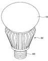
도 1은 실시 예에 의한 조명 장치의 사시도
도 2는 조명 장치의 분해 사시도
도 3은 조명 장치의 정면도
도 4는 조명 장치의 평면도
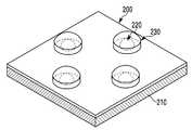
도 5는 광원부의 사시도
도 6은 광원부의 측면도
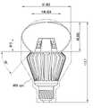
도 7은 렌즈의 치수 예를 나타낸 도면
도 8 및 도 9는 ANSI 규정을 만족하는 실시 예의 조명 장치의 치수를 나타낸 예시도
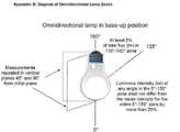
도 10은 미국 후배광 규정의 전방위 램프(Omnidirectional Lamp)의 광도 분포 요구를 설명하기 위한 도면
도 11은 실시 예에 의한 조명 장치의 광도 분포를 시뮬레이션한 결과를 나타낸 그래프
도 12는 기존의 조명 장치의 색좌표를 나타낸 도면
도 13은 실시 예에 의한 조명 장치의 색좌표를 나타낸 도면1 is a perspective view of a lighting apparatus according to an embodiment
2 is an exploded perspective view of the lighting apparatus
3 is a front view of the lighting device
4 is a plan view of the lighting device
5 is a perspective view of a light source unit
6 is a side view of the light source unit
7 shows an example of dimensions of a lens;
8 and 9 are exemplary views showing the dimensions of the lighting device of the embodiment that satisfies the ANSI specification
10 is a view for explaining the luminance distribution request of the omnidirectional lamp of the United States backlight distribution regulations
11 is a graph showing a result of simulating the brightness distribution of the lighting apparatus according to the embodiment
12 is a view showing color coordinates of a conventional lighting device
13 is a view showing color coordinates of the lighting apparatus according to the embodiment
도면에서 각층의 두께나 크기는 설명의 편의 및 명확성을 위하여 과장되거나 생략되거나 또는 개략적으로 도시되었다. 또한 각 구성요소의 크기는 실제크기를 전적으로 반영하는 것은 아니다.The thickness and size of each layer in the drawings are exaggerated, omitted, or schematically shown for convenience and clarity of explanation. In addition, the size of each component does not necessarily reflect the actual size.
본 발명에 따른 실시 예의 설명에 있어서, 각 element의 " 상(위) 또는 하(아래)(on or under)"에 형성되는 것으로 기재되는 경우에 있어, 상(위) 또는 하(아래)(on or under)는 두 개의 element가 서로 직접(directly)접촉되거나 하나 이상의 다른 element가 상기 두 element 사이에 배치되어(indirectly) 형성되는 것을 모두 포함한다. 또한 "상(위) 또는 하(아래)(on or under)"으로 표현되는 경우 하나의 element를 기준으로 위쪽 방향뿐만 아니라 아래쪽 방향의 의미도 포함할 수 있다.In the description of the embodiment according to the present invention, when described as being formed on the "on or under" of each element, the (up) or down (on) or under) includes both two elements being directly contacted with each other or one or more other elements are formed indirectly between the two elements. Also, when expressed as "on or under", it may include not only an upward direction but also a downward direction with respect to one element.
이하, 본 발명에서 실시하고자 하는 구체적인 기술내용에 대해 첨부도면을 참조하여 상세하게 설명하기로 한다.
DETAILED DESCRIPTION OF THE PREFERRED EMBODIMENTS Hereinafter, the present invention will be described in detail with reference to the accompanying drawings.
실시 예Example
도 1은 실시 예에 의한 조명 장치의 사시도이고, 도 2는 조명 장치의 분해 사시도이고, 도 3은 조명 장치의 정면도이고, 도 4는 조명 장치의 평면도이고, 도 5는 광원부의 사시도이고, 도 6은 광원부의 측면도이고, 도 7은 렌즈의 치수 예를 나타낸 도면이다.1 is a perspective view of a lighting apparatus according to an embodiment, FIG. 2 is an exploded perspective view of the lighting apparatus, FIG. 3 is a front view of the lighting apparatus, FIG. 4 is a plan view of the lighting apparatus, FIG. 5 is a perspective view of the light source unit, and FIG. 6 is a side view of the light source unit, and FIG. 7 is a view showing an example of dimensions of the lens.
실시 예의 조명 장치는 도 1 내지 도 4에 도시된 바와 같이, 커버(100), 광원부(200), 방열체(300), 회로부(400), 내부 케이스(500) 및 소켓(600)을 포함하여 구성될 수 있다.1 to 4, the lighting apparatus of the embodiment includes a
상기 커버(100)는 상기 방열체(300) 상에 배치되고, 하부에 개구부(110)가 형성되어 있으며, 속이 비어 있는 벌브(bulb) 형상을 하고 있다. 상기 커버(100)는 상기 방열체(300)와 결합시 상기 개구부(110)를 통해 상기 광원부(200)와 부재(350)를 내부에 삽입하도록 되어 있다. 따라서, 상기 커버(100)가 상기 방열체(300)에 결합되면, 상기 광원부(200)와 상기 부재(350)는 상기 커버(100)에 의해 둘러싸이게 된다.The
상기 커버(100)와 상기 방열체(300)의 결합은 접착제를 통해 결합될 수도 있고, 회전 결합 방식 및 후크 결합 방식 등 다양한 방식으로 결합될 수 있다. 상기 회전 결합 방식은 상기 방열체(300)의 나사홈에 상기 커버(100)의 나사산이 결합하는 방식으로서 상기 커버(100)의 회전에 의해 상기 커버(100)와 상기 방열체(300)가 결합하는 방식이다. 그리고, 상기 후크 결합 방식은 상기 커버(100)의 턱이 상기 방열체(300)의 홈에 끼워져 상기 커버(100)와 상기 방열체(300)가 결합하는 방식이다.The
상기 커버(100)는 상기 방열체(300) 상에 배치되고, 하부에 개구부(110)를 가질 수 있다. 또한, 상기 커버(100)는 상기 하부와 대응되는 상부와, 상기 하부와 상부 사이에 중앙부를 갖고, 상기 하부의 개구부(110)의 지름은 상기 방열체(300)의 상면 지름보다 작거나 같고, 상기 중앙부의 지름은 상기 방열체(300)의 상면 지름보다 크게 형성될 수 있다.The
상기 커버(100)는 상기 광원부(200)와 광학적으로 결합된다. 좀더 구체적으로 설명하면, 상기 커버(100)는 상기 광원부(200)의 발광 소자(220)로부터의 광을 확산, 산란 또는 여기시킬 수 있다. 또한, 일부는 반사하고 일부는 여기시키는 반사물질이 적어도 일부에 배치될 수도 있다. 여기서, 상기 커버(100)는 상기 광원부(200)로부터의 광을 여기시키기 위해, 내부면 또는 외부면 또는 내부 및 외부면 또는 상기 커버(100)의 내부에 형광체를 가질 수 있다.The
또한, 상기 커버(100)는 내부면에 유백색 도료가 코팅될 수 있다. 여기서, 상기 유백색 도료는 빛을 확산시키는 확산재를 포함할 수 있다.In addition, the
또한, 상기 커버(100)는 내부면의 표면 거칠기가 외부면의 표면 거칠기보다 클 수 있다. 이는 상기 광원부(200)로부터의 광을 충분히 산란 및 확산시키기 위함이다.In addition, the surface roughness of the inner surface of the
상기 커버(100)는 유리(glass) 재질이나 플라스틱, 폴리프로필렌(PP), 폴리에틸렌(PE), 폴리카보네이트(PC) 등의 수지재질로 형성될 수 있다. 여기서, 폴리카보네이트(PC)는 내광성, 내열성 및 강도가 우수한 성질을 가지고 있다.The
상기 커버(100)는 외부에서 상기 광원부(200)와 상기 부재(350)가 보일 수 있는 투명한 재질로 형성될 수 있고, 내부가 보이지 않는 불투명한 재질로 형성될 수도 있다. 이와 같은 상기 커버(100)는 블로우(blow) 성형을 통해 형성될 수 있다.The
또한, 상기 커버(100)는 상기 광원부(200)로부터 발광된 광의 적어도 일부를 상기 방열체(300) 방향으로 반사시키는 반사물질을 포함할 수 있다.In addition, the
상기 광원부(200)는 상기 방열체(300) 상에 배치된 상기 부재(350)에 배치될 수 있다. 좀더 구체적으로 설명하면, 상기 광원부(200)는 상기 부재(350)의 측면들 중에 하나 이상의 측면에 배치될 수 있다. 이때, 상기 부재(350)는 소정의 각도(예를 들어, 15°)로 기울어진 측면을 갖는 다각 기둥으로 구성될 수 있다.The
상기 조명 장치는 상기 부재의 측면에 적어도 2개 이상의 광원부(200)가 배치될 수 있다. 실시 예에서는, 상기 부재(350)의 6개 측면 중에서 3개의 측면에 상기 광원부(200)가 배치된 예를 나타내었다. 그러나 이에 한정된 것은 아니고, 상기 부재(350)의 모든 측면에 배치될 수도 있다. 상기 부재(350)의 구성에 대해서는 뒤에서 상세히 설명하기로 한다.At least two
상기 광원부(200)는 기판(210) 상에 적어도 1개 이상의 발광 소자(220)가 배치되어 있다. 실시 예의 도면에서는 하나의 기판(210) 상에 4개의 발광 소자(220)가 대칭 구조로 구성된 예를 나타내었다.At least one light emitting
또한, 상기 광원부(200)는 상기 기판(210)의 발광 소자(220) 상에 배치된 렌즈부(230)를 더 포함할 수 있다. 이때, 상기 렌즈부(230)는 150°또는 160°이상의 빔 각도를 갖는 비구면 렌즈(aspherics)(231)를 포함하고 있다.In addition, the
상기 렌즈부(230)는 도 5 내지 도 7에 도시된 바와 같이, 상기 발광소자(220) 상에 각각 배치된 비구면 렌즈(231)와, 상기 비구면 렌즈(231)와 일체로 형성되며 상기 기판(210) 상에 배치된 바닥면(232)으로 구성될 수 있다. 여기서, 상기 비구면 렌즈(231)는 상기 바닥면(232)에서 수직으로 형성된 원통 형상의 측면(231a)과, 상기 측면(231a)의 상부에 형성된 반구 형상의 곡면(231b)을 이루고 있다.As shown in FIGS. 5 to 7, the
상기 렌즈(231)는 상기 발광소자(220)에서 나오는 광의 지향각을 증가시켜 상기 조명 장치의 선형 광원의 균일성을 향상시킬 수 있다. 상기 렌즈(231)는 오목, 볼록, 반구형 중 선택되는 어느 하나의 형상을 가질 수 있으며, 에폭시 수지, 실리콘수지, 우레탄계 수지 또는 그 혼합물로 형성될 수 있다.The
상기 렌즈부(230)는 다음과 같은 최적화 데이터를 가질 수 있다.The
도 7을 참조하면, 상기 렌즈(231)는 원형(Circular)으로 구성될 수 있고, 상기 렌즈(231)의 배후 표면(Rear Surface)이 비구면을 가질 수 있다. 그리고, 상기 렌즈(231)의 지름(Diameter)이 2.8㎜, 상기 바닥면(232)으로부터 상기 렌즈(231)의 곡면(231b)까지의 높이가 1.2㎜, 상기 바닥면(232)으로부터 상기 렌즈(231)의 측면(231a)까지의 높이가 0.507㎜, 상기 측면(231a) 상단의 지름이 2.86㎜, 상기 렌즈부(230)의 두께가 0.1㎜로 설계될 수 있다. 여기서, 상기 측면(231a) 상단의 지름은 상기 측면(231a)의 높이에 따라 상기 렌즈(231)의 지름보다 크거나 작게 설계될 수 있다.Referring to FIG. 7, the
또한, 상기 렌즈부(230)는 상기 바닥면(232)에 반사층(미도시)이 형성될 수 있다. 이때, 상기 반사층은 금속 예컨대, 알루미늄(Al), 구리(Cu), 백금(Pt), 은(Ag), 티타늄(Ti), 크롬(Cr), 금(Au), 니켈(Ni)을 포함하는 금속물질 중에서 선택된 적어도 어느 한 물질로 단층 또는 복합층으로 증착(deposition), 스퍼터링(sputtering), 도금(plating), 인쇄(printing) 등의 방법으로 형성될 수도 있다.In addition, the
상기 기판(210)은 사각형의 판 형상을 갖지만, 이에 한정되지 않고 원형, 다각형 등 다양한 형태를 가질 수 있다. 상기 기판(210)은 절연체에 회로 패턴이 인쇄된 것일 수 있다. 예를 들어, 인쇄회로기판(PCB: Printed Circuit Board), 메탈 코아(Metal Core) PCB, 연성(Flexible) PCB, 세라믹 PCB 등을 포함할 수 있다. 또한, 상기 기판(210)은 인쇄회로기판 상에 LED 칩을 직접 본딩할 수 있는 COB(Chips On Board) 타입을 사용할 수도 있다. 또한, 상기 기판(210)은 광을 효율적으로 반사하는 재질로 형성되거나, 표면이 광을 효율적으로 반사하는 컬러(예를 들어, 백색, 은색 등)로 형성될 수도 있다. 또한, 상기 기판(210)은 표면이 빛을 효율적으로 반사하는 재질이거나, 빛이 효율적으로 반사되는 컬러(예를 들어, 백색, 은색 등)로 코팅될 수 있다. 예를 들어, 상기 기판(210)은 표면을 통해 빛이 반사되는 반사율이 78% 이상의 특성을 가질 수 있다.The
상기 기판(210)은 상기 방열체(300)에 수납되는 상기 회로부(400)와 전기적으로 연결된다. 상기 기판(210)과 상기 회로부(400)는 와이어(wire)(미도시)를 통해 연결될 수 있다. 이때, 상기 와이어는 상기 방열체(300)를 관통하여 상기 기판(210)과 상기 회로부(400)를 연결한다.The
상기 발광 소자(220)는 적색(Red), 녹색(Green), 청색(Blue)의 광을 방출하는 발광 다이오드(LED) 칩이거나 UV를 방출하는 발광 다이오드(LED) 칩일 수 있다. 여기서, 상기 발광 다이오드(LED) 칩은 수평형(Lateral Type) 또는 수직형(Vertical Type)일 수 있고, 청색(Blue), 적색(Red), 황색(Yellow), 또는 녹색(Green)을 발산할 수 있다.The
상기 발광 소자(220)는 형광체를 가질 수 있다. 상기 형광체는 가넷(Garnet)계(YAG, TAG), 실리케이드(Silicate)계, 나이트라이드(Nitride)계 및 옥시나이트라이드(Oxynitride)계 중 어느 하나 이상일 수 있다. 또는 형광체는 황색 형광체, 녹색 형광체 및 적색 형광체 중 어느 하나 이상일 수도 있다.The
실시 예에서는, 1.3×1.3×0.1의 크기를 가지며, 청색(Blue) LED + 황색(Yellow) 형광체의 특성을 갖는 LED 칩을 사용하였다.In the embodiment, an LED chip having a size of 1.3 × 1.3 × 0.1 and having characteristics of a blue LED + yellow phosphor was used.
상기 방열체(300)는 상기 커버(100)와 결합되고, 상기 광원부(200)로부터의 열을 외부로 방열하는 역할을 한다. 상기 방열체(300)는 소정의 체적을 가지며, 상면(310) 및 몸체(330)를 갖는다. 즉, 상기 방열체(300)는 상면(310)과, 상기 상면(310)과 연결되어 소정의 기울기를 갖는 일부 영역을 포함하는 측면을 갖는 몸체(330)를 포함하고 있다. 이때, 상기 일부 영역의 기울기는 상기 상면(310)과 평행한 가상선을 기준으로 45°이상의 범위를 가질 수 있다.The
상기 방열체(300)의 상면(310)에는 상기 부재(350)가 배치된다. 그리고, 상기 상면(310)은 상기 커버(100)와 결합될 수 있다. 또한, 상기 상면(310)은 상기 커버(100)의 개구(110)와 대응되는 형상을 가질 수 있다.The
상기 방열체(300)는 상기 몸체(330) 외주면에 복수 개의 방열핀(370)이 배치될 수 있고, 상기 방열핀(370)의 적어도 일부가 기울기를 갖는 측면을 형성할 수 있다. 이때, 상기 기울기는 상기 방열체(300)의 상면과 평형한 가상선을 기준으로 45°이상의 범위를 가질 수 있다.The
상기 방열핀(370)은 상기 방열체(300)의 외면에서 외측 방향으로 연장되어 형성되거나 상기 외면에 결합되어 구성될 수도 있다. 이러한 구조를 갖는 상기 방열핀(370)은 모두 상기 방열체(300)의 방열 면적을 넓힘으로써 방열 효율을 향상시킬 수 있다.The radiating
한편, 다른 예로서, 상기 방열체(300)는 상기 방열핀(370)을 갖지 않을 수도 있다.On the other hand, as another example, the
상기 방열체(300)는 상기 회로부(400)와 상기 내부 케이스(500)가 수납되는 수납부(미도시)를 내부에 형성할 수 있다.The
상기 부재(350)는 상기 방열체(300)의 상면(310)에 배치될 수 있다. 이때, 상기 부재(350)는 상기 방열체(300)의 상면(310)과 일체로 형성될 수도 있고, 상기 방열체(300)의 상면(310)에 결합에 의해 구성될 수도 있다.The
상기 부재(350)는 소정의 각도(예를 들어, 15°)로 기울어진 측면을 갖는 다각 기둥 또는 원뿔 기둥으로 구성될 수 있다. 구체적으로, 상기 부재(350)는 육각 기둥일 수 있다. 상기 육각 기둥의 부재(350)는 윗면과 밑면, 그리고 6개의 측면을 갖는다. 또한, 상기 부재(350)는 다각 기둥뿐만 아니라 원 기둥 또는 타원 기둥일 수 있다. 상기 부재(350)가 원 기둥 또는 타원 기둥일 경우, 상기 광원부(200)의 기판(210)은 연성 기판일 수 있다.The
상기 부재(350)의 측면에는 상기 광원부(200)가 배치될 수 있다. 즉, 6개의 측면 모두에 상기 광원부(200)가 배치될 수도 있고, 6개의 측면 중 몇 개의 측면에 상기 광원부(200)가 배치될 수도 있다. 또한, 상기 부재(350)의 측면에 적어도 2개 이상의 광원부(200)가 배치될 수 있다. 실시 예에서는 6개의 측면 중 3개의 측면에 상기 광원부(200)가 배치된 예를 나타내었다.The
실시 예에서는 소정의 각도(예를 들어, 15°)로 기울어진 6개의 측면을 갖는 육각기둥 형태로 구성하고, 상기 6개의 측면 중 3개의 측면에 상기 광원부(200)를 배치함으로써, 광원부의 구배각으로 암부 발생을 제거할 수 있다. 또한, 상기 광원부(200)의 발광소자(220) 상에 160°이상의 빔 각도를 갖는 프라이머리(Primary) 렌즈를 배치하여 후배광 특성을 향상시킬 수 있다.In an embodiment, the
상기 부재(350)는 열 전도성을 갖는 재질로 구성될 수 있다. 이는 상기 광원 부(200)로부터 발생되는 열을 외부로 빠르게 방출하기 위함이다. 상기 부재(350)의 재질은 예를 들어, 알루미늄(Al), 니켈(Ni), 구리(Cu), 마그네슘(Mg), 은(Ag), 주석(Sn) 등과 상기 금속들의 합금일 수 있다. 또는, 열 전도성을 갖는 열 전도성 플라스틱일 수 있다. 상기 열 전도성 플라스틱은 금속보다 무게가 가볍고, 단방향성의 열 전도성을 갖는 이점이 있다.The
상기 회로부(400)는 외부로부터 전원을 공급받고, 공급받은 전원을 상기 광원부(200)에 맞게 변환하여 상기 광원부(200)로 공급한다.The
상기 회로부(400)는 상기 방열체(300) 내부에 배치된다. 구체적으로, 상기 회로부(400)는 상기 내부 케이스(500)에 수납되어 상기 내부 케이스(500)와 함께 상기 방열체(300)의 수납부(미도시)에 수납된다.The
상기 회로부(400)는 상기 회로 기판(410)과, 상기 회로 기판(410) 상에 탑재되는 다수의 부품(430)들을 포함하여 구성될 수 있다.The
상기 회로 기판(410)은 사각형의 판 형상을 갖지만, 이에 한정되지 않고 다양한 형태를 가질 수 있다. 예를 들면, 원형, 타원형 또는 다각형의 판 형상일 수 있다. 이러한 상기 회로 기판(410)은 절연체에 회로 패턴이 인쇄된 것일 수 있다.The
상기 회로 기판(410)은 상기 광원부(200)의 기판(210)과 전기적으로 연결된다. 상기 회로 기판(410)과 상기 기판(210)의 전기적 연결은 와이어(wire)를 통해 연결될 수 있다. 상기 와이어는 상기 방열체(300)의 내부에 배치되어 상기 회로 기판(410)과 상기 기판(210)을 연결할 수 있다.The
상기 다수의 부품(430)들은 예를 들어, 외부 전원으로부터 제공되는 교류 전원을 직류 전원으로 변환하는 직류변환장치와, 상기 광원부(200)의 구동을 제어하는 구동칩과, 상기 광원부(200)를 보호하기 위한 ESD(ElectroStatic discharge) 보호 소자 등을 포함할 수 있다.The plurality of
상기 내부 케이스(500)는 내부에 상기 회로부(400)를 수납한다. 상기 내부 케이스(500)는 상기 회로부(400)를 수납하기 위해 수납부(510)를 가질 수 있다. 상기 수납부(510)는 원통 형상을 가질 수 있으나 상기 방열체(300)의 수납부(미도시)의 형상에 따라 달라질 수도 있다.The
상기 내부 케이스(500)는 상기 방열체(300) 내부에 수납된다. 더 구체적으로, 상기 내부 케이스(500)의 수납부(510)는 상기 방열체(300)의 하면(미도시)에 형성된 수납부(미도시)에 수납된다.The
상기 내부 케이스(500)는 상기 소켓(600)과 결합된다. 상기 내부 케이스(500)는 상기 소켓(600)과 결합하는 연결부(530)를 가질 수 있다. 상기 연결부(530)는 상기 소켓(600)의 나사홈 구조와 대응되는 나사산 구조를 가질 수 있다.The
상기 내부 케이스(500)는 부도체로 구성될 수 있다. 따라서, 상기 회로부(400)와 상기 방열체(300) 사이의 전기적 단락을 방지할 수 있다. 이러한 상기 내부 케이스(500)는 플라스틱 또는 수지 재질로 구성될 수 있다.The
상기 소켓(600)은 상기 내부 케이스(500)와 결합된다. 더 구체적으로, 상기 소켓(600)은 상기 내부 케이스(500)의 연결부(530)와 결합된다.The
상기 소켓(600)은 종래의 재래식 백열 전구와 같은 구조를 가질 수 있다. 상기 소켓(600)은 상기 회로부(400)와 전기적으로 연결된다. 이때, 상기 회로부(400)와 상기 소켓(600)의 전기적 연결은 와이어(wire)를 통해 연결될 수 있다. 따라서, 상기 소켓(600)에 외부 전원이 인가되면, 상기 소켓(600)을 통해 상기 회로부(400)로 외부 전원이 공급되고, 상기 회로부(400)에서 변환된 전원이 상기 광원부(200)로 공급되게 된다.The
상기 소켓(600)은 상기 연결부(530)의 나사산 구조과 대응되는 나사홈 구조를 가질 수 있다.The
상술한 바와 같이, 실시 예의 조명 장치는 상기 방열체(300) 상에 소정의 각도(15°)로 측면이 기울어진 부재(350)를 배치하고, 상기 부재(350)의 측면에 적어도 1개 이상의 광원부(200)를 배치하고, 상기 광원부(200)의 발광소자(220) 상에 렌즈(231)를 배치함으로써, 미국 후배광 규정(Energy star) 및 ANSI 규정을 만족하면서도 후배광 특성을 구현할 수 있으며 암부를 제거할 수 있다.
As described above, in the lighting apparatus of the embodiment, the
미국 후배광 규정(Energy Star) 및 ANSI 규정US Backlighting Regulation (Energy Star) and ANSI Regulations
도 8 및 도 9는 ANSI 규정을 만족하는 실시 예의 조명 장치의 치수를 나타낸 예시도이고, 도 10은 미국 후배광 규정(Energy Star)의 전방위 램프(Omnidirectional Lamp)의 광도 분포 요구를 설명하기 위한 도면이다.8 and 9 are exemplary diagrams showing the dimensions of the lighting device of the embodiment that satisfies the ANSI regulations, and FIG. 10 is a view for explaining the luminance distribution request of the omnidirectional lamp of the Energy Star. to be.
상기 ANSI 규정은 미국의 공업 기구물에 대한 규격 또는 기준을 미리 지정해 놓은 것을 말한다. 상기 ANSI 규정에는, 실시 예의 조명 장치와 같은 기구물에 대해서도 그 기준을 마련해 놓고 있다.The ANSI regulations mean that specifications or standards for industrial equipment in the United States are specified in advance. In the ANSI regulation, the standard is also provided for a fixture such as the lighting apparatus of the embodiment.
실시 예에 따른 조명 장치는 ANSI 규정을 만족하기 위해서, 상기 조명 장치의 전체 높이, 상기 커버(100)의 높이, 상기 커버(100)의 지름, 상기 방열체(300)의 상면의 지름, 상기 부재(350)의 높이, 상기 부재(350)의 측면 하나의 길이가 7.5∼7.6 : 3.3∼3.4 : 4.5∼4.6 : 2.7∼2.8 : 2.2∼2.3 : 1의 비율을 가질 수 있다.In order to satisfy the ANSI standard, the lighting apparatus according to the embodiment may include an overall height of the lighting apparatus, a height of the
도 8 및 도 9를 참조하면, 실시 예에 따른 조명 장치는, 상기 소켓(600)에서 상기 커버(100)까지의 높이가 112.7㎜, 상기 커버(100)의 높이가 48.956㎜, 상기 커버(100)의 지름이 67.855㎜, 상기 방열체(300)의 상면(310)의 지름이 40.924㎜, 상기 부재(350)의 높이가 32.6㎜, 상기 부재(350)의 측면 하나의 길이가 15㎜를 가짐으로써, 일점 쇄선으로 표시된 ANSI 규정을 만족하는 것을 알 수 있다.8 and 9, in the lighting apparatus according to the embodiment, the height from the
한편, 상기 미국 후배광 규정(Energy Star)은 조명 장치 또는 조명 기구가 소정의 광도(luminous intensity) 분포(distribution)를 가져야 한다는 규정이다. 상기 미국 후배광 규정(Energy Star)에서, 전방위 램프(Omnidirectional Lamp)의 광도 분포 요구는 도 10과 같다.On the other hand, the United States Energy Back Light Regulation (Energy Star) is a rule that the lighting device or lighting fixture should have a predetermined luminous intensity distribution. In the US Starlight Regulation (Energy Star), the luminance distribution request of the omnidirectional lamp is shown in FIG.
도 10에 도시된 미국 후배광 규정(Energy Star)을 참조하면, 조명 장치의 135°와 180°사이에서는 적어도 전체 광속(flux(lmens))의 5%가 발광되어야 한다는 요구가 있다.Referring to the US Post Light Emitting Regulation (Energy Star) shown in FIG. 10, there is a requirement that at least 5% of the total flux (lmens) should be emitted between 135 ° and 180 ° of the lighting device.
실시 예의 조명 장치는 도 10에 도시된 미국 후배광 규정(Energy Star), 특히 조명 장치의 135°와 180° 사이에서 적어도 전체 광속(flux(lmens))의 5%가 발광되어야 한다는 요구를 만족하고 있음을 다음의 시뮬레이션 결과를 통해 확인하였다.
The lighting device of the embodiment satisfies the requirement of the US Energy Star shown in FIG. 10, in particular at least 5% of the total flux (lmens), between 135 ° and 180 ° of the lighting device. It was confirmed by the following simulation results.
시뮬레이션 결과Simulation result
도 11은 실시 예에 의한 조명 장치의 광도 분포를 시뮬레이션한 결과를 나타낸 그래프이다. 이때, 상기 시뮬레이션은 전체 전력이 667.98Im, 광 효능(Efficiency)이 0.89783, 최대 강도가 60.698cd의 조건으로 실시되었다.11 is a graph showing a result of simulating the brightness distribution of the lighting apparatus according to the embodiment. In this case, the simulation was performed under the condition that the total power is 667.98 Im, the light efficiency is 0.89783, and the maximum intensity is 60.698 cd.
도 11의 시뮬레이션 결과에서도 확인할 수 있듯이, 실시 예의 조명 장치는 광도(luminous intensity) 분포(distribution)가 전체적으로 균일하게 분포하고 있어, 미국 후배광 규정(Energy Star)에서 요구하고 있는 후배광 특성을 만족하고 있음을 보여주고 있다.As can be seen from the simulation results of FIG. 11, the illumination device of the embodiment has a uniform distribution of luminous intensity throughout, which satisfies the post-light distribution characteristic required by the US Star Light Regulation (Energy Star). It is shown.
다음으로, 도 12는 기존의 조명 장치의 색좌표를 나타낸 도면이고, 도 13은 실시 예에 의한 조명 장치의 색좌표를 나타낸 도면이다. 여기서, 도 12의 색좌표는 실시 예에서 구현한 부재(350)와 렌즈(231)가 설치되어 있지 않은 기존의 조명 장치를 가지고 실험한 결과이고, 도 13의 색좌표는 부재(350)와 렌즈(231)가 설치된 실시 예의 조명 장치를 가지고 실험한 결과이다.Next, FIG. 12 is a view showing color coordinates of a conventional lighting device, and FIG. 13 is a view showing color coordinates of a lighting device according to an embodiment. Here, the color coordinate of FIG. 12 is a result of experimenting with an existing lighting device in which the
먼저, 기존의 조명 장치는 도 12의 색좌표에서 볼 수 있듯이, 최대 조도(Max Illuminance)가 29143.988이고, 중심 조도(Center Illuminance)가 15463.635이고, 전체 평균 조도가 53.6%로 나타났으며, 중심부에 암부가 존재하고 있음이 확인되었다. 이에 반하여, 실시 예의 조명 장치는 도 13의 색좌표에서 볼 수 있듯이, 최대 조도(Max Illuminance)가 48505.615이고, 중심 조도(Center Illuminance)가 42812.934이고, 전체 평균 조도가 88.26%로 나타났으며, 중심부에 암부가 발견되지 않았다.First, as shown in the color coordinates of FIG. 12, the existing lighting device has a maximum illumination of 29143.988, a center illumination of 15463.635, and an overall average illuminance of 53.6%. It was confirmed that it exists. In contrast, the illumination device of the embodiment has a maximum illumination of 48505.615, a center illumination of 42812.934, and an overall average illuminance of 88.26%, as shown in the color coordinates of FIG. 13. No dark areas found.
따라서, 상기 색좌표에서도 확인할 수 있듯이, 실시 예의 조명 장치는 기존의 조명 장치에 비해 후배광 특성이 크게 개선되었고, 기존에 존재하던 암부도 크게 줄어들었음을 시뮬레이션 결과를 통해 확인할 수 있었다.
Therefore, as can be seen in the color coordinates, the lighting device of the embodiment was confirmed that the post-light distribution characteristics are significantly improved compared to the conventional lighting device, and the existing dark part was also significantly reduced through simulation results.
이와 같이 구성된 실시 예에 따른 조명 장치는, 방열체 상에 소정의 각도로 측면이 기울어진 부재를 배치하고, 상기 부재의 측면에 광원부를 배치하고, 상기 광원부의 발광소자 상에 렌즈를 배치함으로써, 본 발명의 기술적 과제를 해결할 수가 있다.
In the lighting apparatus according to the embodiment configured as described above, by arranging a member inclined side by a predetermined angle on the radiator, the light source portion is disposed on the side surface of the member, the lens is disposed on the light emitting element of the light source portion, The technical problem of this invention can be solved.
이상에서 실시 예를 중심으로 설명하였으나 이는 단지 예시일 뿐 본 발명을 한정하는 것이 아니며, 본 발명이 속하는 분야의 통상의 지식을 가진 자라면 본 실시 예의 본질적인 특성을 벗어나지 않는 범위에서 이상에 예시되지 않은 여러 가지의 변형과 응용이 가능함을 알 수 있을 것이다. 예를 들어, 실시 예에 구체적으로 나타난 각 구성 요소는 변형하여 실시할 수 있는 것이다. 그리고 이러한 변형과 응용에 관계된 차이점들은 첨부된 청구 범위에서 규정하는 본 발명의 범위에 포함되는 것으로 해석되어야 할 것이다.
Although the above description has been made with reference to the embodiments, these are merely examples and are not intended to limit the present invention. Those skilled in the art to which the present invention pertains are not illustrated above without departing from the essential characteristics of the present embodiments. It will be appreciated that many variations and applications are possible. For example, each component specifically shown in the embodiments can be modified and implemented. It is to be understood that all changes and modifications that come within the meaning and range of equivalency of the claims are therefore intended to be embraced therein.
100 : 커버110 : 개구부
200 : 광원부210 : 기판
220 : 발광소자230 : 렌즈부
231 : 렌즈231a : 측면
231b : 곡면232 : 바닥면
300 : 방열체310 : 상면
330 : 몸체350 : 부재
370 : 방열핀400 : 회로부
410 : 회로기판430 : 부품
500 : 내부 케이스510 : 수납부
530 : 연결부600 : 소켓100: cover 110: opening
200: light source unit 210: substrate
220: light emitting element 230: lens unit
231:
231b curved surface 232: bottom surface
300: radiator 310: upper surface
330
370: heat sink fin 400: circuit
410: circuit board 430: parts
500: inner case 510: storage
530: connection 600: socket
Claims (20)
Translated fromKorean상기 방열체 상에 배치되고 측면을 갖는 부재;
상기 부재의 측면에 배치되고, 기판과 상기 기판상에 배치된 발광소자를 갖는 광원부;
상기 발광소자 상에 배치되고 빔 지향각이 150°이상인 렌즈와 상기 렌즈와 일체로 형성되며 상기 기판 상에 배치되고, 반사층이 형성되어 있는 바닥면을 포함하는 렌즈부; 및
상기 방열체상에 배치되고 하부에 개구부를 갖는 커버;
를 포함하는 조명 장치.
Heat sink;
A member disposed on the heat sink and having a side surface;
A light source unit disposed on a side of the member and having a substrate and a light emitting element disposed on the substrate;
A lens unit including a lens disposed on the light emitting element and having a beam directing angle of 150 ° or more and integrally formed with the lens and disposed on the substrate and having a reflective layer formed thereon; And
A cover disposed on the heat sink and having an opening at a bottom thereof;
≪ / RTI >
상기 부재는 기둥 형상을 갖고,
상기 측면은 소정의 각도로 기울어진 조명 장치.
The method of claim 1,
The member has a columnar shape,
The side surface is inclined at a predetermined angle.
상기 소정의 각도는 15°인 조명 장치.
3. The method of claim 2,
The predetermined angle is 15 °.
상기 부재는 사각, 오각, 육각, 팔각을 포함한 다각 기둥 중 하나이거나 원뿔 기둥인 조명 장치.
3. The method of claim 2,
The member is one of a polygonal pillar, including a square, pentagonal, hexagonal, octagonal or conical pillar.
상기 조명 장치는 상기 부재의 측면에 적어도 2개 이상의 광원부가 배치된 조명 장치.
The method according to any one of claims 1 to 4,
The lighting device is at least two light source is disposed on the side of the member.
상기 부재는 육각 기둥으로서 6개의 측면 중 3개의 측면에 상기 광원부가 배치된 조명 장치.
The method according to any one of claims 1 to 4,
The member is a hexagonal pillar, wherein the light source is disposed on three of the six sides.
상기 부재는 알루미늄(Al), 니켈(Ni), 구리(Cu), 마그네슘(Mg), 은(Ag), 주석(Sn)을 포함한 금속 또는 이들 금속의 합금 중 어느 하나로 구성된 조명 장치.
The method according to any one of claims 1 to 4,
The member is made of any one of metals including aluminum (Al), nickel (Ni), copper (Cu), magnesium (Mg), silver (Ag), tin (Sn) or alloys of these metals.
상기 부재는 열 전도성을 갖는 열 전도성 수지재질로 구성된 조명 장치.
The method according to any one of claims 1 to 4,
The member is made of a thermally conductive resin material having a thermal conductivity.
상기 방열체는, 상면과, 상기 상면과 연결되어 소정의 기울기를 갖는 일부 영역을 포함하는 측면을 갖는 몸체를 포함하고, 상기 일부 영역의 기울기는 상기 상면과 평형한 가상선을 기준으로 45°이상을 갖는 조명 장치.
The method of claim 1,
The radiator includes a body having a top surface and a side surface connected to the top surface and including a partial region having a predetermined slope, wherein the slope of the partial region is 45 ° or more based on an imaginary line parallel to the top surface. Lighting device having a.
상기 발광소자는 LED 칩 또는 UV LED 칩인 조명 장치.
The method of claim 1,
The light emitting device is an LED chip or a UV LED chip.
상기 렌즈는 비구면 렌즈(aspherics)인 조명 장치.
The method of claim 1,
Wherein said lens is an aspheric lens.
상기 방열체 상에 배치되고 측면을 갖는 부재;
상기 부재의 측면에 배치되고, 기판과 상기 기판상에 배치된 발광소자를 갖는 광원부;
상기 발광소자 상에 배치되고 빔 지향각이 150°이상인 렌즈를 갖는 렌즈부; 및
상기 방열체상에 배치되고 하부에 개구부를 갖는 커버를 포함하는 조명 장치이고,
상기 조명 장치의 전체 높이, 상기 커버의 높이, 상기 커버의 지름, 상기 방열체의 상면의 지름, 상기 부재의 높이, 상기 부재의 측면 하나의 길이가 7.5∼7.6 : 3.3∼3.4 : 4.5∼4.6 : 2.7∼2.8 : 2.2∼2.3 : 1의 비율을 갖는 조명 장치.
Heat sink;
A member disposed on the heat sink and having a side surface;
A light source unit disposed on a side of the member and having a substrate and a light emitting element disposed on the substrate;
A lens unit disposed on the light emitting element and having a lens having a beam directing angle of 150 ° or more; And
Is disposed on the radiator and a lighting device including a cover having an opening in the lower,
The overall height of the lighting device, the height of the cover, the diameter of the cover, the diameter of the upper surface of the heat sink, the height of the member, and the length of one side of the member are 7.5 to 7.6: 3.3 to 3.4: 4.5 to 4.6: A lighting device having a ratio of 2.7 to 2.8: 2.2 to 2.3: 1.
상기 방열체 상에 배치되고 측면을 갖는 부재;
상기 부재의 측면에 배치되고, 기판과 상기 기판상에 배치된 발광소자를 갖는 광원부;
상기 발광소자 상에 배치되고 빔 지향각이 150°이상인 렌즈와 상기 렌즈와 일체로 형성되며 상기 기판 상에 배치된 바닥면을 포함하는 렌즈부; 및
상기 방열체상에 배치되고 하부에 개구부를 갖는 커버를 포함하고,
상기 렌즈는 오목, 볼록, 반구형 중 선택된 어느 하나의 형상을 가지며,
상기 렌즈 및 바닥면은 에폭시 수지, 실리콘 수지, 우레탄계 수지 중 어느 하나이거나 그 혼합물로 이루어진 조명 장치.
Heat sink;
A member disposed on the heat sink and having a side surface;
A light source unit disposed on a side of the member and having a substrate and a light emitting element disposed on the substrate;
A lens unit disposed on the light emitting device and having a beam directing angle of 150 ° or more, and a lens unit integrally formed with the lens and having a bottom surface disposed on the substrate; And
A cover disposed on the heat sink and having an opening at the bottom thereof;
The lens has a shape of any one selected from concave, convex, hemispherical,
The lens and the bottom surface is any one of an epoxy resin, silicone resin, urethane-based resin or a mixture thereof.
상기 하부와 대응되는 상부와, 상기 하부와 상부 사이에 중앙부를 갖고, 상기 하부의 상기 개구부의 지름은 상기 방열체의 상면 지름보다 작거나 같고, 상기 중앙부의 지름은 상기 방열체의 상면 지름보다 큰 조명 장치.
The method of claim 1, wherein the cover is:
An upper portion corresponding to the lower portion, and a central portion between the lower portion and the upper portion, the diameter of the opening of the lower portion is smaller than or equal to the upper diameter of the upper surface of the heat sink, and the diameter of the central portion is larger than the upper diameter of the upper surface of the heat sink. Lighting device.
상기 커버는 내부 면, 외부 면 또는 내부 및 외부 면 또는 내부에 적어도 하나 이상의 형광체를 포함하는 조명 장치.
17. The method of claim 16,
And the cover comprises at least one phosphor on an inner surface, an outer surface, or an inner and an outer surface or interior.
상기 커버는 상기 광원부로부터 발광된 광의 적어도 일부를 상기 방열체 방향으로 반사시키는 반사물질을 포함하는 조명 장치.
17. The method of claim 16,
The cover includes a reflecting material for reflecting at least a portion of the light emitted from the light source in the direction of the radiator.
상기 방열체는 상기 몸체 외주면에 복수 개의 방열핀이 배치되고, 상기 방열핀의 적어도 일부가 상기 기울기를 갖는 측면을 형성하는 조명 장치.
The method of claim 9,
The radiator has a plurality of radiating fins disposed on the outer peripheral surface of the body, at least a portion of the radiating fins to form a side having the slope.
상기 방열체 상에 배치되고 소정의 기울기를 갖는 측면을 포함한 부재;
상기 부재의 측면에 배치되고, 기판과 상기 기판상에 발광소자를 갖는 광원부; 및
상기 발광소자 상에 배치된 렌즈와 상기 렌즈와 일체로 형성되며 상기 기판 상에 매치되고, 반사층이 형성되어 있는 바닥면을 포함하는 렌즈부;
를 포함하고,
상기 부재는 원기둥 또는 다각 기둥형상을 갖고,
상기 렌즈는 원통형상의 측면과 상기 측면상에 곡면 형상을 포함하는 곡면부를 갖고,
상기 방열체는 상면과 상기 상면의 평행한 가상의 직선을 기준으로 기울어진 기울기를 갖는 측면을 갖는 몸체를 포함하는 조명 장치.Heat sink;
A member including a side surface disposed on the heat sink and having a predetermined slope;
A light source unit disposed on a side of the member and having a substrate and a light emitting element on the substrate; And
A lens unit integrally formed with the lens disposed on the light emitting device and the lens, the lens unit including a bottom surface that is matched on the substrate and has a reflective layer formed thereon;
Lt; / RTI >
The member has a cylindrical or polygonal columnar shape,
The lens has a cylindrical side and a curved portion including a curved shape on the side,
The radiator includes a body having a side having a slope inclined based on a parallel virtual straight line of the upper surface and the upper surface.
Priority Applications (14)
| Application Number | Priority Date | Filing Date | Title |
|---|---|---|---|
| KR1020110140134AKR101326518B1 (en) | 2011-09-02 | 2011-12-22 | Lighting device |
| CN201611150040.XACN107013820B (en) | 2011-09-02 | 2012-08-31 | Lighting device |
| CN201280042711.4ACN103765081B (en) | 2011-09-02 | 2012-08-31 | Lighting device |
| EP12828129.2AEP2751472B1 (en) | 2011-09-02 | 2012-08-31 | Lighting device |
| EP22152540.5AEP4006405A1 (en) | 2011-09-02 | 2012-08-31 | Lighting device |
| PCT/KR2012/006995WO2013032276A1 (en) | 2011-09-02 | 2012-08-31 | Lighting device |
| JP2014528285AJP6193234B2 (en) | 2011-09-02 | 2012-08-31 | Lighting device |
| US13/583,752US8905580B2 (en) | 2011-09-02 | 2012-08-31 | Lighting device |
| US14/532,682US9353914B2 (en) | 2011-09-02 | 2014-11-04 | Lighting device |
| US15/096,992US9719671B2 (en) | 2011-09-02 | 2016-04-12 | Lighting device |
| US15/633,294US9970644B2 (en) | 2011-09-02 | 2017-06-26 | Lighting device |
| JP2017153785AJP6427639B2 (en) | 2011-09-02 | 2017-08-09 | Lighting device |
| US15/946,420US10260724B2 (en) | 2011-09-02 | 2018-04-05 | Lighting device |
| JP2018202993AJP6637574B2 (en) | 2011-09-02 | 2018-10-29 | Lighting equipment |
Applications Claiming Priority (2)
| Application Number | Priority Date | Filing Date | Title |
|---|---|---|---|
| KR1020110088970AKR101293928B1 (en) | 2011-09-02 | 2011-09-02 | Lighting device |
| KR1020110140134AKR101326518B1 (en) | 2011-09-02 | 2011-12-22 | Lighting device |
Publications (2)
| Publication Number | Publication Date |
|---|---|
| KR20130072623A KR20130072623A (en) | 2013-07-02 |
| KR101326518B1true KR101326518B1 (en) | 2013-11-07 |
Family
ID=47756599
Family Applications (1)
| Application Number | Title | Priority Date | Filing Date |
|---|---|---|---|
| KR1020110140134AExpired - Fee RelatedKR101326518B1 (en) | 2011-09-02 | 2011-12-22 | Lighting device |
Country Status (6)
| Country | Link |
|---|---|
| US (5) | US8905580B2 (en) |
| EP (2) | EP2751472B1 (en) |
| JP (3) | JP6193234B2 (en) |
| KR (1) | KR101326518B1 (en) |
| CN (2) | CN103765081B (en) |
| WO (1) | WO2013032276A1 (en) |
Families Citing this family (319)
| Publication number | Priority date | Publication date | Assignee | Title |
|---|---|---|---|---|
| US9394608B2 (en) | 2009-04-06 | 2016-07-19 | Asm America, Inc. | Semiconductor processing reactor and components thereof |
| US8802201B2 (en) | 2009-08-14 | 2014-08-12 | Asm America, Inc. | Systems and methods for thin-film deposition of metal oxides using excited nitrogen-oxygen species |
| US20130023129A1 (en) | 2011-07-20 | 2013-01-24 | Asm America, Inc. | Pressure transmitter for a semiconductor processing environment |
| KR101326518B1 (en)* | 2011-09-02 | 2013-11-07 | 엘지이노텍 주식회사 | Lighting device |
| US9017481B1 (en) | 2011-10-28 | 2015-04-28 | Asm America, Inc. | Process feed management for semiconductor substrate processing |
| US10714315B2 (en) | 2012-10-12 | 2020-07-14 | Asm Ip Holdings B.V. | Semiconductor reaction chamber showerhead |
| US20160376700A1 (en) | 2013-02-01 | 2016-12-29 | Asm Ip Holding B.V. | System for treatment of deposition reactor |
| KR20140101220A (en)* | 2013-02-08 | 2014-08-19 | 삼성전자주식회사 | Lighting device |
| KR102077232B1 (en)* | 2013-03-07 | 2020-02-13 | 삼성전자주식회사 | Lighting device |
| US9644799B2 (en)* | 2013-03-13 | 2017-05-09 | Smartbotics Inc. | LED light bulb construction and manufacture |
| KR102089625B1 (en)* | 2013-07-31 | 2020-03-16 | 엘지이노텍 주식회사 | Lighting device |
| US11015245B2 (en) | 2014-03-19 | 2021-05-25 | Asm Ip Holding B.V. | Gas-phase reactor and system having exhaust plenum and components thereof |
| GB201407301D0 (en)* | 2014-04-25 | 2014-06-11 | Aurora Ltd | Improved led lamps and luminaires |
| US10858737B2 (en) | 2014-07-28 | 2020-12-08 | Asm Ip Holding B.V. | Showerhead assembly and components thereof |
| US9890456B2 (en) | 2014-08-21 | 2018-02-13 | Asm Ip Holding B.V. | Method and system for in situ formation of gas-phase compounds |
| US10941490B2 (en) | 2014-10-07 | 2021-03-09 | Asm Ip Holding B.V. | Multiple temperature range susceptor, assembly, reactor and system including the susceptor, and methods of using the same |
| US10276355B2 (en) | 2015-03-12 | 2019-04-30 | Asm Ip Holding B.V. | Multi-zone reactor, system including the reactor, and method of using the same |
| CN104879669A (en)* | 2015-06-19 | 2015-09-02 | 厦门李氏兄弟有限公司 | LED filament lamp |
| US10458018B2 (en) | 2015-06-26 | 2019-10-29 | Asm Ip Holding B.V. | Structures including metal carbide material, devices including the structures, and methods of forming same |
| US10295162B2 (en)* | 2015-10-20 | 2019-05-21 | Philippe Georges Habchi | Modular light bulb with quick and easily user-replaceable independent components |
| US10211308B2 (en) | 2015-10-21 | 2019-02-19 | Asm Ip Holding B.V. | NbMC layers |
| US11139308B2 (en) | 2015-12-29 | 2021-10-05 | Asm Ip Holding B.V. | Atomic layer deposition of III-V compounds to form V-NAND devices |
| US10529554B2 (en) | 2016-02-19 | 2020-01-07 | Asm Ip Holding B.V. | Method for forming silicon nitride film selectively on sidewalls or flat surfaces of trenches |
| US10343920B2 (en) | 2016-03-18 | 2019-07-09 | Asm Ip Holding B.V. | Aligned carbon nanotubes |
| US10865475B2 (en) | 2016-04-21 | 2020-12-15 | Asm Ip Holding B.V. | Deposition of metal borides and silicides |
| US10190213B2 (en) | 2016-04-21 | 2019-01-29 | Asm Ip Holding B.V. | Deposition of metal borides |
| US10367080B2 (en) | 2016-05-02 | 2019-07-30 | Asm Ip Holding B.V. | Method of forming a germanium oxynitride film |
| US11453943B2 (en) | 2016-05-25 | 2022-09-27 | Asm Ip Holding B.V. | Method for forming carbon-containing silicon/metal oxide or nitride film by ALD using silicon precursor and hydrocarbon precursor |
| US9859151B1 (en) | 2016-07-08 | 2018-01-02 | Asm Ip Holding B.V. | Selective film deposition method to form air gaps |
| US10612137B2 (en) | 2016-07-08 | 2020-04-07 | Asm Ip Holdings B.V. | Organic reactants for atomic layer deposition |
| JP6765241B2 (en)* | 2016-07-13 | 2020-10-07 | 株式会社小糸製作所 | Lighting device for vehicles |
| US10714385B2 (en) | 2016-07-19 | 2020-07-14 | Asm Ip Holding B.V. | Selective deposition of tungsten |
| US9887082B1 (en) | 2016-07-28 | 2018-02-06 | Asm Ip Holding B.V. | Method and apparatus for filling a gap |
| KR102532607B1 (en) | 2016-07-28 | 2023-05-15 | 에이에스엠 아이피 홀딩 비.브이. | Substrate processing apparatus and method of operating the same |
| US9812320B1 (en) | 2016-07-28 | 2017-11-07 | Asm Ip Holding B.V. | Method and apparatus for filling a gap |
| US10643826B2 (en) | 2016-10-26 | 2020-05-05 | Asm Ip Holdings B.V. | Methods for thermally calibrating reaction chambers |
| US11532757B2 (en) | 2016-10-27 | 2022-12-20 | Asm Ip Holding B.V. | Deposition of charge trapping layers |
| US10714350B2 (en) | 2016-11-01 | 2020-07-14 | ASM IP Holdings, B.V. | Methods for forming a transition metal niobium nitride film on a substrate by atomic layer deposition and related semiconductor device structures |
| US10229833B2 (en) | 2016-11-01 | 2019-03-12 | Asm Ip Holding B.V. | Methods for forming a transition metal nitride film on a substrate by atomic layer deposition and related semiconductor device structures |
| IT201600111812A1 (en)* | 2016-11-07 | 2018-05-07 | Philed S R L | LIGHTING DEVICE IN LED TECHNOLOGY AND ITS MANUFACTURING PROCEDURE |
| KR102546317B1 (en) | 2016-11-15 | 2023-06-21 | 에이에스엠 아이피 홀딩 비.브이. | Gas supply unit and substrate processing apparatus including the same |
| KR102762543B1 (en) | 2016-12-14 | 2025-02-05 | 에이에스엠 아이피 홀딩 비.브이. | Substrate processing apparatus |
| US11447861B2 (en) | 2016-12-15 | 2022-09-20 | Asm Ip Holding B.V. | Sequential infiltration synthesis apparatus and a method of forming a patterned structure |
| US11581186B2 (en) | 2016-12-15 | 2023-02-14 | Asm Ip Holding B.V. | Sequential infiltration synthesis apparatus |
| KR102700194B1 (en) | 2016-12-19 | 2024-08-28 | 에이에스엠 아이피 홀딩 비.브이. | Substrate processing apparatus |
| CN108224103A (en)* | 2016-12-21 | 2018-06-29 | 苏州欧普照明有限公司 | A kind of light supply apparatus |
| US10269558B2 (en) | 2016-12-22 | 2019-04-23 | Asm Ip Holding B.V. | Method of forming a structure on a substrate |
| US10867788B2 (en) | 2016-12-28 | 2020-12-15 | Asm Ip Holding B.V. | Method of forming a structure on a substrate |
| US11390950B2 (en) | 2017-01-10 | 2022-07-19 | Asm Ip Holding B.V. | Reactor system and method to reduce residue buildup during a film deposition process |
| US10468261B2 (en) | 2017-02-15 | 2019-11-05 | Asm Ip Holding B.V. | Methods for forming a metallic film on a substrate by cyclical deposition and related semiconductor device structures |
| US10529563B2 (en) | 2017-03-29 | 2020-01-07 | Asm Ip Holdings B.V. | Method for forming doped metal oxide films on a substrate by cyclical deposition and related semiconductor device structures |
| KR102457289B1 (en) | 2017-04-25 | 2022-10-21 | 에이에스엠 아이피 홀딩 비.브이. | Method for depositing a thin film and manufacturing a semiconductor device |
| US10488028B2 (en)* | 2017-05-03 | 2019-11-26 | Fluence Bioengineering, Inc. | Systems and methods for a heat sink |
| US10892156B2 (en) | 2017-05-08 | 2021-01-12 | Asm Ip Holding B.V. | Methods for forming a silicon nitride film on a substrate and related semiconductor device structures |
| US10770286B2 (en) | 2017-05-08 | 2020-09-08 | Asm Ip Holdings B.V. | Methods for selectively forming a silicon nitride film on a substrate and related semiconductor device structures |
| US10886123B2 (en) | 2017-06-02 | 2021-01-05 | Asm Ip Holding B.V. | Methods for forming low temperature semiconductor layers and related semiconductor device structures |
| US12040200B2 (en) | 2017-06-20 | 2024-07-16 | Asm Ip Holding B.V. | Semiconductor processing apparatus and methods for calibrating a semiconductor processing apparatus |
| US11306395B2 (en) | 2017-06-28 | 2022-04-19 | Asm Ip Holding B.V. | Methods for depositing a transition metal nitride film on a substrate by atomic layer deposition and related deposition apparatus |
| US10685834B2 (en) | 2017-07-05 | 2020-06-16 | Asm Ip Holdings B.V. | Methods for forming a silicon germanium tin layer and related semiconductor device structures |
| KR20190009245A (en) | 2017-07-18 | 2019-01-28 | 에이에스엠 아이피 홀딩 비.브이. | Methods for forming a semiconductor device structure and related semiconductor device structures |
| US11018002B2 (en) | 2017-07-19 | 2021-05-25 | Asm Ip Holding B.V. | Method for selectively depositing a Group IV semiconductor and related semiconductor device structures |
| US11374112B2 (en) | 2017-07-19 | 2022-06-28 | Asm Ip Holding B.V. | Method for depositing a group IV semiconductor and related semiconductor device structures |
| US10541333B2 (en) | 2017-07-19 | 2020-01-21 | Asm Ip Holding B.V. | Method for depositing a group IV semiconductor and related semiconductor device structures |
| US10590535B2 (en) | 2017-07-26 | 2020-03-17 | Asm Ip Holdings B.V. | Chemical treatment, deposition and/or infiltration apparatus and method for using the same |
| TWI815813B (en) | 2017-08-04 | 2023-09-21 | 荷蘭商Asm智慧財產控股公司 | Showerhead assembly for distributing a gas within a reaction chamber |
| US10770336B2 (en) | 2017-08-08 | 2020-09-08 | Asm Ip Holding B.V. | Substrate lift mechanism and reactor including same |
| US10692741B2 (en) | 2017-08-08 | 2020-06-23 | Asm Ip Holdings B.V. | Radiation shield |
| US11769682B2 (en) | 2017-08-09 | 2023-09-26 | Asm Ip Holding B.V. | Storage apparatus for storing cassettes for substrates and processing apparatus equipped therewith |
| US11139191B2 (en) | 2017-08-09 | 2021-10-05 | Asm Ip Holding B.V. | Storage apparatus for storing cassettes for substrates and processing apparatus equipped therewith |
| USD900036S1 (en)* | 2017-08-24 | 2020-10-27 | Asm Ip Holding B.V. | Heater electrical connector and adapter |
| US11830730B2 (en) | 2017-08-29 | 2023-11-28 | Asm Ip Holding B.V. | Layer forming method and apparatus |
| US11056344B2 (en) | 2017-08-30 | 2021-07-06 | Asm Ip Holding B.V. | Layer forming method |
| US11295980B2 (en) | 2017-08-30 | 2022-04-05 | Asm Ip Holding B.V. | Methods for depositing a molybdenum metal film over a dielectric surface of a substrate by a cyclical deposition process and related semiconductor device structures |
| KR102491945B1 (en) | 2017-08-30 | 2023-01-26 | 에이에스엠 아이피 홀딩 비.브이. | Substrate processing apparatus |
| KR102401446B1 (en) | 2017-08-31 | 2022-05-24 | 에이에스엠 아이피 홀딩 비.브이. | Substrate processing apparatus |
| KR102630301B1 (en) | 2017-09-21 | 2024-01-29 | 에이에스엠 아이피 홀딩 비.브이. | Method of sequential infiltration synthesis treatment of infiltrateable material and structures and devices formed using same |
| US10844484B2 (en) | 2017-09-22 | 2020-11-24 | Asm Ip Holding B.V. | Apparatus for dispensing a vapor phase reactant to a reaction chamber and related methods |
| US10658205B2 (en) | 2017-09-28 | 2020-05-19 | Asm Ip Holdings B.V. | Chemical dispensing apparatus and methods for dispensing a chemical to a reaction chamber |
| US10403504B2 (en) | 2017-10-05 | 2019-09-03 | Asm Ip Holding B.V. | Method for selectively depositing a metallic film on a substrate |
| US10319588B2 (en) | 2017-10-10 | 2019-06-11 | Asm Ip Holding B.V. | Method for depositing a metal chalcogenide on a substrate by cyclical deposition |
| US10923344B2 (en) | 2017-10-30 | 2021-02-16 | Asm Ip Holding B.V. | Methods for forming a semiconductor structure and related semiconductor structures |
| US10910262B2 (en) | 2017-11-16 | 2021-02-02 | Asm Ip Holding B.V. | Method of selectively depositing a capping layer structure on a semiconductor device structure |
| CN107940311A (en)* | 2017-11-20 | 2018-04-20 | 江门市云达灯饰有限公司 | A kind of luminescence component of garden lamp |
| US11022879B2 (en) | 2017-11-24 | 2021-06-01 | Asm Ip Holding B.V. | Method of forming an enhanced unexposed photoresist layer |
| CN111344522B (en) | 2017-11-27 | 2022-04-12 | 阿斯莫Ip控股公司 | Including clean mini-environment device |
| WO2019103613A1 (en) | 2017-11-27 | 2019-05-31 | Asm Ip Holding B.V. | A storage device for storing wafer cassettes for use with a batch furnace |
| US10872771B2 (en) | 2018-01-16 | 2020-12-22 | Asm Ip Holding B. V. | Method for depositing a material film on a substrate within a reaction chamber by a cyclical deposition process and related device structures |
| KR102695659B1 (en) | 2018-01-19 | 2024-08-14 | 에이에스엠 아이피 홀딩 비.브이. | Method for depositing a gap filling layer by plasma assisted deposition |
| TWI799494B (en) | 2018-01-19 | 2023-04-21 | 荷蘭商Asm 智慧財產控股公司 | Deposition method |
| US11018047B2 (en) | 2018-01-25 | 2021-05-25 | Asm Ip Holding B.V. | Hybrid lift pin |
| USD880437S1 (en) | 2018-02-01 | 2020-04-07 | Asm Ip Holding B.V. | Gas supply plate for semiconductor manufacturing apparatus |
| US11081345B2 (en) | 2018-02-06 | 2021-08-03 | Asm Ip Holding B.V. | Method of post-deposition treatment for silicon oxide film |
| WO2019158960A1 (en) | 2018-02-14 | 2019-08-22 | Asm Ip Holding B.V. | A method for depositing a ruthenium-containing film on a substrate by a cyclical deposition process |
| US10896820B2 (en) | 2018-02-14 | 2021-01-19 | Asm Ip Holding B.V. | Method for depositing a ruthenium-containing film on a substrate by a cyclical deposition process |
| US10731249B2 (en) | 2018-02-15 | 2020-08-04 | Asm Ip Holding B.V. | Method of forming a transition metal containing film on a substrate by a cyclical deposition process, a method for supplying a transition metal halide compound to a reaction chamber, and related vapor deposition apparatus |
| KR102636427B1 (en) | 2018-02-20 | 2024-02-13 | 에이에스엠 아이피 홀딩 비.브이. | Substrate processing method and apparatus |
| US10975470B2 (en) | 2018-02-23 | 2021-04-13 | Asm Ip Holding B.V. | Apparatus for detecting or monitoring for a chemical precursor in a high temperature environment |
| US11473195B2 (en) | 2018-03-01 | 2022-10-18 | Asm Ip Holding B.V. | Semiconductor processing apparatus and a method for processing a substrate |
| US11629406B2 (en) | 2018-03-09 | 2023-04-18 | Asm Ip Holding B.V. | Semiconductor processing apparatus comprising one or more pyrometers for measuring a temperature of a substrate during transfer of the substrate |
| US11114283B2 (en) | 2018-03-16 | 2021-09-07 | Asm Ip Holding B.V. | Reactor, system including the reactor, and methods of manufacturing and using same |
| KR102646467B1 (en) | 2018-03-27 | 2024-03-11 | 에이에스엠 아이피 홀딩 비.브이. | Method of forming an electrode on a substrate and a semiconductor device structure including an electrode |
| US11088002B2 (en) | 2018-03-29 | 2021-08-10 | Asm Ip Holding B.V. | Substrate rack and a substrate processing system and method |
| US11230766B2 (en) | 2018-03-29 | 2022-01-25 | Asm Ip Holding B.V. | Substrate processing apparatus and method |
| KR102501472B1 (en) | 2018-03-30 | 2023-02-20 | 에이에스엠 아이피 홀딩 비.브이. | Substrate processing method |
| KR102600229B1 (en) | 2018-04-09 | 2023-11-10 | 에이에스엠 아이피 홀딩 비.브이. | Substrate supporting device, substrate processing apparatus including the same and substrate processing method |
| TWI811348B (en) | 2018-05-08 | 2023-08-11 | 荷蘭商Asm 智慧財產控股公司 | Methods for depositing an oxide film on a substrate by a cyclical deposition process and related device structures |
| US12025484B2 (en) | 2018-05-08 | 2024-07-02 | Asm Ip Holding B.V. | Thin film forming method |
| US12272527B2 (en) | 2018-05-09 | 2025-04-08 | Asm Ip Holding B.V. | Apparatus for use with hydrogen radicals and method of using same |
| KR20190129718A (en) | 2018-05-11 | 2019-11-20 | 에이에스엠 아이피 홀딩 비.브이. | Methods for forming a doped metal carbide film on a substrate and related semiconductor device structures |
| KR102596988B1 (en) | 2018-05-28 | 2023-10-31 | 에이에스엠 아이피 홀딩 비.브이. | Method of processing a substrate and a device manufactured by the same |
| TWI840362B (en) | 2018-06-04 | 2024-05-01 | 荷蘭商Asm Ip私人控股有限公司 | Wafer handling chamber with moisture reduction |
| US11718913B2 (en) | 2018-06-04 | 2023-08-08 | Asm Ip Holding B.V. | Gas distribution system and reactor system including same |
| US11286562B2 (en) | 2018-06-08 | 2022-03-29 | Asm Ip Holding B.V. | Gas-phase chemical reactor and method of using same |
| US10797133B2 (en) | 2018-06-21 | 2020-10-06 | Asm Ip Holding B.V. | Method for depositing a phosphorus doped silicon arsenide film and related semiconductor device structures |
| KR102568797B1 (en) | 2018-06-21 | 2023-08-21 | 에이에스엠 아이피 홀딩 비.브이. | Substrate processing system |
| TWI873894B (en) | 2018-06-27 | 2025-02-21 | 荷蘭商Asm Ip私人控股有限公司 | Cyclic deposition methods for forming metal-containing material and films and structures including the metal-containing material |
| KR102854019B1 (en) | 2018-06-27 | 2025-09-02 | 에이에스엠 아이피 홀딩 비.브이. | Periodic deposition method for forming a metal-containing material and films and structures comprising the metal-containing material |
| KR102686758B1 (en) | 2018-06-29 | 2024-07-18 | 에이에스엠 아이피 홀딩 비.브이. | Method for depositing a thin film and manufacturing a semiconductor device |
| US10612136B2 (en) | 2018-06-29 | 2020-04-07 | ASM IP Holding, B.V. | Temperature-controlled flange and reactor system including same |
| US10755922B2 (en) | 2018-07-03 | 2020-08-25 | Asm Ip Holding B.V. | Method for depositing silicon-free carbon-containing film as gap-fill layer by pulse plasma-assisted deposition |
| US10388513B1 (en) | 2018-07-03 | 2019-08-20 | Asm Ip Holding B.V. | Method for depositing silicon-free carbon-containing film as gap-fill layer by pulse plasma-assisted deposition |
| US10767789B2 (en) | 2018-07-16 | 2020-09-08 | Asm Ip Holding B.V. | Diaphragm valves, valve components, and methods for forming valve components |
| US11053591B2 (en) | 2018-08-06 | 2021-07-06 | Asm Ip Holding B.V. | Multi-port gas injection system and reactor system including same |
| US10883175B2 (en) | 2018-08-09 | 2021-01-05 | Asm Ip Holding B.V. | Vertical furnace for processing substrates and a liner for use therein |
| US10829852B2 (en) | 2018-08-16 | 2020-11-10 | Asm Ip Holding B.V. | Gas distribution device for a wafer processing apparatus |
| US11430674B2 (en) | 2018-08-22 | 2022-08-30 | Asm Ip Holding B.V. | Sensor array, apparatus for dispensing a vapor phase reactant to a reaction chamber and related methods |
| US11024523B2 (en) | 2018-09-11 | 2021-06-01 | Asm Ip Holding B.V. | Substrate processing apparatus and method |
| KR102707956B1 (en) | 2018-09-11 | 2024-09-19 | 에이에스엠 아이피 홀딩 비.브이. | Method for deposition of a thin film |
| US11049751B2 (en) | 2018-09-14 | 2021-06-29 | Asm Ip Holding B.V. | Cassette supply system to store and handle cassettes and processing apparatus equipped therewith |
| CN110970344B (en) | 2018-10-01 | 2024-10-25 | Asmip控股有限公司 | Substrate holding apparatus, system comprising the same and method of using the same |
| US11232963B2 (en) | 2018-10-03 | 2022-01-25 | Asm Ip Holding B.V. | Substrate processing apparatus and method |
| KR102592699B1 (en) | 2018-10-08 | 2023-10-23 | 에이에스엠 아이피 홀딩 비.브이. | Substrate support unit and apparatuses for depositing thin film and processing the substrate including the same |
| US10847365B2 (en) | 2018-10-11 | 2020-11-24 | Asm Ip Holding B.V. | Method of forming conformal silicon carbide film by cyclic CVD |
| US10811256B2 (en) | 2018-10-16 | 2020-10-20 | Asm Ip Holding B.V. | Method for etching a carbon-containing feature |
| KR102605121B1 (en) | 2018-10-19 | 2023-11-23 | 에이에스엠 아이피 홀딩 비.브이. | Substrate processing apparatus and substrate processing method |
| KR102546322B1 (en) | 2018-10-19 | 2023-06-21 | 에이에스엠 아이피 홀딩 비.브이. | Substrate processing apparatus and substrate processing method |
| USD948463S1 (en) | 2018-10-24 | 2022-04-12 | Asm Ip Holding B.V. | Susceptor for semiconductor substrate supporting apparatus |
| US12378665B2 (en) | 2018-10-26 | 2025-08-05 | Asm Ip Holding B.V. | High temperature coatings for a preclean and etch apparatus and related methods |
| US11087997B2 (en) | 2018-10-31 | 2021-08-10 | Asm Ip Holding B.V. | Substrate processing apparatus for processing substrates |
| KR102748291B1 (en) | 2018-11-02 | 2024-12-31 | 에이에스엠 아이피 홀딩 비.브이. | Substrate support unit and substrate processing apparatus including the same |
| US11572620B2 (en) | 2018-11-06 | 2023-02-07 | Asm Ip Holding B.V. | Methods for selectively depositing an amorphous silicon film on a substrate |
| US11031242B2 (en) | 2018-11-07 | 2021-06-08 | Asm Ip Holding B.V. | Methods for depositing a boron doped silicon germanium film |
| US10847366B2 (en) | 2018-11-16 | 2020-11-24 | Asm Ip Holding B.V. | Methods for depositing a transition metal chalcogenide film on a substrate by a cyclical deposition process |
| US10818758B2 (en) | 2018-11-16 | 2020-10-27 | Asm Ip Holding B.V. | Methods for forming a metal silicate film on a substrate in a reaction chamber and related semiconductor device structures |
| US12040199B2 (en) | 2018-11-28 | 2024-07-16 | Asm Ip Holding B.V. | Substrate processing apparatus for processing substrates |
| US11217444B2 (en) | 2018-11-30 | 2022-01-04 | Asm Ip Holding B.V. | Method for forming an ultraviolet radiation responsive metal oxide-containing film |
| KR102636428B1 (en) | 2018-12-04 | 2024-02-13 | 에이에스엠 아이피 홀딩 비.브이. | A method for cleaning a substrate processing apparatus |
| US11158513B2 (en) | 2018-12-13 | 2021-10-26 | Asm Ip Holding B.V. | Methods for forming a rhenium-containing film on a substrate by a cyclical deposition process and related semiconductor device structures |
| TWI874340B (en) | 2018-12-14 | 2025-03-01 | 荷蘭商Asm Ip私人控股有限公司 | Method of forming device structure, structure formed by the method and system for performing the method |
| TWI866480B (en) | 2019-01-17 | 2024-12-11 | 荷蘭商Asm Ip 私人控股有限公司 | Methods of forming a transition metal containing film on a substrate by a cyclical deposition process |
| KR102727227B1 (en) | 2019-01-22 | 2024-11-07 | 에이에스엠 아이피 홀딩 비.브이. | Semiconductor processing device |
| CN111524788B (en) | 2019-02-01 | 2023-11-24 | Asm Ip私人控股有限公司 | Method for forming topologically selective films of silicon oxide |
| TWI838458B (en) | 2019-02-20 | 2024-04-11 | 荷蘭商Asm Ip私人控股有限公司 | Apparatus and methods for plug fill deposition in 3-d nand applications |
| TWI845607B (en) | 2019-02-20 | 2024-06-21 | 荷蘭商Asm Ip私人控股有限公司 | Cyclical deposition method and apparatus for filling a recess formed within a substrate surface |
| KR102626263B1 (en) | 2019-02-20 | 2024-01-16 | 에이에스엠 아이피 홀딩 비.브이. | Cyclical deposition method including treatment step and apparatus for same |
| TWI873122B (en) | 2019-02-20 | 2025-02-21 | 荷蘭商Asm Ip私人控股有限公司 | Method of filling a recess formed within a surface of a substrate, semiconductor structure formed according to the method, and semiconductor processing apparatus |
| TWI842826B (en) | 2019-02-22 | 2024-05-21 | 荷蘭商Asm Ip私人控股有限公司 | Substrate processing apparatus and method for processing substrate |
| KR102782593B1 (en) | 2019-03-08 | 2025-03-14 | 에이에스엠 아이피 홀딩 비.브이. | Structure Including SiOC Layer and Method of Forming Same |
| US11742198B2 (en) | 2019-03-08 | 2023-08-29 | Asm Ip Holding B.V. | Structure including SiOCN layer and method of forming same |
| KR102858005B1 (en) | 2019-03-08 | 2025-09-09 | 에이에스엠 아이피 홀딩 비.브이. | Method for Selective Deposition of Silicon Nitride Layer and Structure Including Selectively-Deposited Silicon Nitride Layer |
| JP2020167398A (en) | 2019-03-28 | 2020-10-08 | エーエスエム・アイピー・ホールディング・ベー・フェー | Door openers and substrate processing equipment provided with door openers |
| KR102809999B1 (en) | 2019-04-01 | 2025-05-19 | 에이에스엠 아이피 홀딩 비.브이. | Method of manufacturing semiconductor device |
| KR20200123380A (en) | 2019-04-19 | 2020-10-29 | 에이에스엠 아이피 홀딩 비.브이. | Layer forming method and apparatus |
| KR20200125453A (en) | 2019-04-24 | 2020-11-04 | 에이에스엠 아이피 홀딩 비.브이. | Gas-phase reactor system and method of using same |
| KR20200130121A (en) | 2019-05-07 | 2020-11-18 | 에이에스엠 아이피 홀딩 비.브이. | Chemical source vessel with dip tube |
| US11289326B2 (en) | 2019-05-07 | 2022-03-29 | Asm Ip Holding B.V. | Method for reforming amorphous carbon polymer film |
| KR20200130652A (en) | 2019-05-10 | 2020-11-19 | 에이에스엠 아이피 홀딩 비.브이. | Method of depositing material onto a surface and structure formed according to the method |
| JP7598201B2 (en) | 2019-05-16 | 2024-12-11 | エーエスエム・アイピー・ホールディング・ベー・フェー | Wafer boat handling apparatus, vertical batch furnace and method |
| JP7612342B2 (en) | 2019-05-16 | 2025-01-14 | エーエスエム・アイピー・ホールディング・ベー・フェー | Wafer boat handling apparatus, vertical batch furnace and method |
| USD975665S1 (en) | 2019-05-17 | 2023-01-17 | Asm Ip Holding B.V. | Susceptor shaft |
| USD947913S1 (en) | 2019-05-17 | 2022-04-05 | Asm Ip Holding B.V. | Susceptor shaft |
| EP3973226B1 (en) | 2019-05-20 | 2023-11-15 | Signify Holding B.V. | A light source comprising a substrate and a heat sink structure |
| USD935572S1 (en) | 2019-05-24 | 2021-11-09 | Asm Ip Holding B.V. | Gas channel plate |
| USD922229S1 (en) | 2019-06-05 | 2021-06-15 | Asm Ip Holding B.V. | Device for controlling a temperature of a gas supply unit |
| KR20200141002A (en) | 2019-06-06 | 2020-12-17 | 에이에스엠 아이피 홀딩 비.브이. | Method of using a gas-phase reactor system including analyzing exhausted gas |
| KR20200141931A (en) | 2019-06-10 | 2020-12-21 | 에이에스엠 아이피 홀딩 비.브이. | Method for cleaning quartz epitaxial chambers |
| KR20200143254A (en) | 2019-06-11 | 2020-12-23 | 에이에스엠 아이피 홀딩 비.브이. | Method of forming an electronic structure using an reforming gas, system for performing the method, and structure formed using the method |
| USD944946S1 (en) | 2019-06-14 | 2022-03-01 | Asm Ip Holding B.V. | Shower plate |
| USD931978S1 (en) | 2019-06-27 | 2021-09-28 | Asm Ip Holding B.V. | Showerhead vacuum transport |
| KR20210005515A (en) | 2019-07-03 | 2021-01-14 | 에이에스엠 아이피 홀딩 비.브이. | Temperature control assembly for substrate processing apparatus and method of using same |
| JP7499079B2 (en) | 2019-07-09 | 2024-06-13 | エーエスエム・アイピー・ホールディング・ベー・フェー | Plasma device using coaxial waveguide and substrate processing method |
| CN112216646A (en) | 2019-07-10 | 2021-01-12 | Asm Ip私人控股有限公司 | Substrate supporting assembly and substrate processing device comprising same |
| KR20210010307A (en) | 2019-07-16 | 2021-01-27 | 에이에스엠 아이피 홀딩 비.브이. | Substrate processing apparatus |
| KR20210010816A (en) | 2019-07-17 | 2021-01-28 | 에이에스엠 아이피 홀딩 비.브이. | Radical assist ignition plasma system and method |
| KR102860110B1 (en) | 2019-07-17 | 2025-09-16 | 에이에스엠 아이피 홀딩 비.브이. | Methods of forming silicon germanium structures |
| US11643724B2 (en) | 2019-07-18 | 2023-05-09 | Asm Ip Holding B.V. | Method of forming structures using a neutral beam |
| KR20210010817A (en) | 2019-07-19 | 2021-01-28 | 에이에스엠 아이피 홀딩 비.브이. | Method of Forming Topology-Controlled Amorphous Carbon Polymer Film |
| TWI839544B (en) | 2019-07-19 | 2024-04-21 | 荷蘭商Asm Ip私人控股有限公司 | Method of forming topology-controlled amorphous carbon polymer film |
| TWI851767B (en) | 2019-07-29 | 2024-08-11 | 荷蘭商Asm Ip私人控股有限公司 | Methods for selective deposition utilizing n-type dopants and/or alternative dopants to achieve high dopant incorporation |
| CN112309900A (en) | 2019-07-30 | 2021-02-02 | Asm Ip私人控股有限公司 | Substrate processing apparatus |
| CN112309899A (en) | 2019-07-30 | 2021-02-02 | Asm Ip私人控股有限公司 | Substrate processing apparatus |
| US12169361B2 (en) | 2019-07-30 | 2024-12-17 | Asm Ip Holding B.V. | Substrate processing apparatus and method |
| US11587815B2 (en) | 2019-07-31 | 2023-02-21 | Asm Ip Holding B.V. | Vertical batch furnace assembly |
| US11227782B2 (en) | 2019-07-31 | 2022-01-18 | Asm Ip Holding B.V. | Vertical batch furnace assembly |
| US11587814B2 (en) | 2019-07-31 | 2023-02-21 | Asm Ip Holding B.V. | Vertical batch furnace assembly |
| CN112323048B (en) | 2019-08-05 | 2024-02-09 | Asm Ip私人控股有限公司 | Liquid level sensor for chemical source container |
| CN112342526A (en) | 2019-08-09 | 2021-02-09 | Asm Ip私人控股有限公司 | Heater assembly including cooling device and method of using same |
| USD965044S1 (en) | 2019-08-19 | 2022-09-27 | Asm Ip Holding B.V. | Susceptor shaft |
| USD965524S1 (en) | 2019-08-19 | 2022-10-04 | Asm Ip Holding B.V. | Susceptor support |
| JP2021031769A (en) | 2019-08-21 | 2021-03-01 | エーエスエム アイピー ホールディング ビー.ブイ. | Production apparatus of mixed gas of film deposition raw material and film deposition apparatus |
| USD949319S1 (en) | 2019-08-22 | 2022-04-19 | Asm Ip Holding B.V. | Exhaust duct |
| USD930782S1 (en) | 2019-08-22 | 2021-09-14 | Asm Ip Holding B.V. | Gas distributor |
| USD979506S1 (en) | 2019-08-22 | 2023-02-28 | Asm Ip Holding B.V. | Insulator |
| USD940837S1 (en) | 2019-08-22 | 2022-01-11 | Asm Ip Holding B.V. | Electrode |
| KR20210024423A (en) | 2019-08-22 | 2021-03-05 | 에이에스엠 아이피 홀딩 비.브이. | Method for forming a structure with a hole |
| KR20210024420A (en) | 2019-08-23 | 2021-03-05 | 에이에스엠 아이피 홀딩 비.브이. | Method for depositing silicon oxide film having improved quality by peald using bis(diethylamino)silane |
| US11286558B2 (en) | 2019-08-23 | 2022-03-29 | Asm Ip Holding B.V. | Methods for depositing a molybdenum nitride film on a surface of a substrate by a cyclical deposition process and related semiconductor device structures including a molybdenum nitride film |
| KR102806450B1 (en) | 2019-09-04 | 2025-05-12 | 에이에스엠 아이피 홀딩 비.브이. | Methods for selective deposition using a sacrificial capping layer |
| KR102733104B1 (en) | 2019-09-05 | 2024-11-22 | 에이에스엠 아이피 홀딩 비.브이. | Substrate processing apparatus |
| US11562901B2 (en) | 2019-09-25 | 2023-01-24 | Asm Ip Holding B.V. | Substrate processing method |
| CN112593212B (en) | 2019-10-02 | 2023-12-22 | Asm Ip私人控股有限公司 | Method for forming topologically selective silicon oxide film by cyclic plasma enhanced deposition process |
| TWI846953B (en) | 2019-10-08 | 2024-07-01 | 荷蘭商Asm Ip私人控股有限公司 | Substrate processing device |
| TW202128273A (en) | 2019-10-08 | 2021-08-01 | 荷蘭商Asm Ip私人控股有限公司 | Gas injection system, reactor system, and method of depositing material on surface of substratewithin reaction chamber |
| KR20210042810A (en) | 2019-10-08 | 2021-04-20 | 에이에스엠 아이피 홀딩 비.브이. | Reactor system including a gas distribution assembly for use with activated species and method of using same |
| TWI846966B (en) | 2019-10-10 | 2024-07-01 | 荷蘭商Asm Ip私人控股有限公司 | Method of forming a photoresist underlayer and structure including same |
| US12009241B2 (en) | 2019-10-14 | 2024-06-11 | Asm Ip Holding B.V. | Vertical batch furnace assembly with detector to detect cassette |
| TWI834919B (en) | 2019-10-16 | 2024-03-11 | 荷蘭商Asm Ip私人控股有限公司 | Method of topology-selective film formation of silicon oxide |
| US11637014B2 (en) | 2019-10-17 | 2023-04-25 | Asm Ip Holding B.V. | Methods for selective deposition of doped semiconductor material |
| KR102845724B1 (en) | 2019-10-21 | 2025-08-13 | 에이에스엠 아이피 홀딩 비.브이. | Apparatus and methods for selectively etching films |
| KR20210050453A (en) | 2019-10-25 | 2021-05-07 | 에이에스엠 아이피 홀딩 비.브이. | Methods for filling a gap feature on a substrate surface and related semiconductor structures |
| US11646205B2 (en) | 2019-10-29 | 2023-05-09 | Asm Ip Holding B.V. | Methods of selectively forming n-type doped material on a surface, systems for selectively forming n-type doped material, and structures formed using same |
| KR20210054983A (en) | 2019-11-05 | 2021-05-14 | 에이에스엠 아이피 홀딩 비.브이. | Structures with doped semiconductor layers and methods and systems for forming same |
| US11501968B2 (en) | 2019-11-15 | 2022-11-15 | Asm Ip Holding B.V. | Method for providing a semiconductor device with silicon filled gaps |
| KR102861314B1 (en) | 2019-11-20 | 2025-09-17 | 에이에스엠 아이피 홀딩 비.브이. | Method of depositing carbon-containing material on a surface of a substrate, structure formed using the method, and system for forming the structure |
| US11450529B2 (en) | 2019-11-26 | 2022-09-20 | Asm Ip Holding B.V. | Methods for selectively forming a target film on a substrate comprising a first dielectric surface and a second metallic surface |
| CN112951697B (en) | 2019-11-26 | 2025-07-29 | Asmip私人控股有限公司 | Substrate processing apparatus |
| CN120432376A (en) | 2019-11-29 | 2025-08-05 | Asm Ip私人控股有限公司 | Substrate processing apparatus |
| CN112885692B (en) | 2019-11-29 | 2025-08-15 | Asmip私人控股有限公司 | Substrate processing apparatus |
| JP7527928B2 (en) | 2019-12-02 | 2024-08-05 | エーエスエム・アイピー・ホールディング・ベー・フェー | Substrate processing apparatus and substrate processing method |
| KR20210070898A (en) | 2019-12-04 | 2021-06-15 | 에이에스엠 아이피 홀딩 비.브이. | Substrate processing apparatus |
| KR20210078405A (en) | 2019-12-17 | 2021-06-28 | 에이에스엠 아이피 홀딩 비.브이. | Method of forming vanadium nitride layer and structure including the vanadium nitride layer |
| KR20210080214A (en) | 2019-12-19 | 2021-06-30 | 에이에스엠 아이피 홀딩 비.브이. | Methods for filling a gap feature on a substrate and related semiconductor structures |
| JP7730637B2 (en) | 2020-01-06 | 2025-08-28 | エーエスエム・アイピー・ホールディング・ベー・フェー | Gas delivery assembly, components thereof, and reactor system including same |
| JP7636892B2 (en) | 2020-01-06 | 2025-02-27 | エーエスエム・アイピー・ホールディング・ベー・フェー | Channeled Lift Pins |
| US11993847B2 (en) | 2020-01-08 | 2024-05-28 | Asm Ip Holding B.V. | Injector |
| KR20210093163A (en) | 2020-01-16 | 2021-07-27 | 에이에스엠 아이피 홀딩 비.브이. | Method of forming high aspect ratio features |
| KR102675856B1 (en) | 2020-01-20 | 2024-06-17 | 에이에스엠 아이피 홀딩 비.브이. | Method of forming thin film and method of modifying surface of thin film |
| TWI889744B (en) | 2020-01-29 | 2025-07-11 | 荷蘭商Asm Ip私人控股有限公司 | Contaminant trap system, and baffle plate stack |
| TW202513845A (en) | 2020-02-03 | 2025-04-01 | 荷蘭商Asm Ip私人控股有限公司 | Semiconductor structures and methods for forming the same |
| KR20210100010A (en) | 2020-02-04 | 2021-08-13 | 에이에스엠 아이피 홀딩 비.브이. | Method and apparatus for transmittance measurements of large articles |
| US11776846B2 (en) | 2020-02-07 | 2023-10-03 | Asm Ip Holding B.V. | Methods for depositing gap filling fluids and related systems and devices |
| KR20210103956A (en) | 2020-02-13 | 2021-08-24 | 에이에스엠 아이피 홀딩 비.브이. | Substrate processing apparatus including light receiving device and calibration method of light receiving device |
| TW202146691A (en) | 2020-02-13 | 2021-12-16 | 荷蘭商Asm Ip私人控股有限公司 | Gas distribution assembly, shower plate assembly, and method of adjusting conductance of gas to reaction chamber |
| TWI855223B (en) | 2020-02-17 | 2024-09-11 | 荷蘭商Asm Ip私人控股有限公司 | Method for growing phosphorous-doped silicon layer |
| CN113410160A (en) | 2020-02-28 | 2021-09-17 | Asm Ip私人控股有限公司 | System specially used for cleaning parts |
| KR20210113043A (en) | 2020-03-04 | 2021-09-15 | 에이에스엠 아이피 홀딩 비.브이. | Alignment fixture for a reactor system |
| US11876356B2 (en) | 2020-03-11 | 2024-01-16 | Asm Ip Holding B.V. | Lockout tagout assembly and system and method of using same |
| KR20210116240A (en) | 2020-03-11 | 2021-09-27 | 에이에스엠 아이피 홀딩 비.브이. | Substrate handling device with adjustable joints |
| KR102775390B1 (en) | 2020-03-12 | 2025-02-28 | 에이에스엠 아이피 홀딩 비.브이. | Method for Fabricating Layer Structure Having Target Topological Profile |
| US12173404B2 (en) | 2020-03-17 | 2024-12-24 | Asm Ip Holding B.V. | Method of depositing epitaxial material, structure formed using the method, and system for performing the method |
| KR102755229B1 (en) | 2020-04-02 | 2025-01-14 | 에이에스엠 아이피 홀딩 비.브이. | Thin film forming method |
| TWI887376B (en) | 2020-04-03 | 2025-06-21 | 荷蘭商Asm Ip私人控股有限公司 | Method for manufacturing semiconductor device |
| TWI888525B (en) | 2020-04-08 | 2025-07-01 | 荷蘭商Asm Ip私人控股有限公司 | Apparatus and methods for selectively etching silcon oxide films |
| KR20210128343A (en) | 2020-04-15 | 2021-10-26 | 에이에스엠 아이피 홀딩 비.브이. | Method of forming chromium nitride layer and structure including the chromium nitride layer |
| US11821078B2 (en) | 2020-04-15 | 2023-11-21 | Asm Ip Holding B.V. | Method for forming precoat film and method for forming silicon-containing film |
| US11996289B2 (en) | 2020-04-16 | 2024-05-28 | Asm Ip Holding B.V. | Methods of forming structures including silicon germanium and silicon layers, devices formed using the methods, and systems for performing the methods |
| KR20210130646A (en) | 2020-04-21 | 2021-11-01 | 에이에스엠 아이피 홀딩 비.브이. | Method for processing a substrate |
| CN113555279A (en) | 2020-04-24 | 2021-10-26 | Asm Ip私人控股有限公司 | Methods of forming vanadium nitride-containing layers and structures comprising the same |
| KR20210132600A (en) | 2020-04-24 | 2021-11-04 | 에이에스엠 아이피 홀딩 비.브이. | Methods and systems for depositing a layer comprising vanadium, nitrogen, and a further element |
| KR20210132612A (en) | 2020-04-24 | 2021-11-04 | 에이에스엠 아이피 홀딩 비.브이. | Methods and apparatus for stabilizing vanadium compounds |
| KR102866804B1 (en) | 2020-04-24 | 2025-09-30 | 에이에스엠 아이피 홀딩 비.브이. | Vertical batch furnace assembly comprising a cooling gas supply |
| TW202208671A (en) | 2020-04-24 | 2022-03-01 | 荷蘭商Asm Ip私人控股有限公司 | Methods of forming structures including vanadium boride and vanadium phosphide layers |
| KR102783898B1 (en) | 2020-04-29 | 2025-03-18 | 에이에스엠 아이피 홀딩 비.브이. | Solid source precursor vessel |
| KR20210134869A (en) | 2020-05-01 | 2021-11-11 | 에이에스엠 아이피 홀딩 비.브이. | Fast FOUP swapping with a FOUP handler |
| JP7726664B2 (en) | 2020-05-04 | 2025-08-20 | エーエスエム・アイピー・ホールディング・ベー・フェー | Substrate processing system for processing a substrate |
| KR102788543B1 (en) | 2020-05-13 | 2025-03-27 | 에이에스엠 아이피 홀딩 비.브이. | Laser alignment fixture for a reactor system |
| TW202146699A (en) | 2020-05-15 | 2021-12-16 | 荷蘭商Asm Ip私人控股有限公司 | Method of forming a silicon germanium layer, semiconductor structure, semiconductor device, method of forming a deposition layer, and deposition system |
| KR20210143653A (en) | 2020-05-19 | 2021-11-29 | 에이에스엠 아이피 홀딩 비.브이. | Substrate processing apparatus |
| KR102795476B1 (en) | 2020-05-21 | 2025-04-11 | 에이에스엠 아이피 홀딩 비.브이. | Structures including multiple carbon layers and methods of forming and using same |
| KR20210145079A (en) | 2020-05-21 | 2021-12-01 | 에이에스엠 아이피 홀딩 비.브이. | Flange and apparatus for processing substrates |
| TWI873343B (en) | 2020-05-22 | 2025-02-21 | 荷蘭商Asm Ip私人控股有限公司 | Reaction system for forming thin film on substrate |
| KR20210146802A (en) | 2020-05-26 | 2021-12-06 | 에이에스엠 아이피 홀딩 비.브이. | Method for depositing boron and gallium containing silicon germanium layers |
| TWI876048B (en) | 2020-05-29 | 2025-03-11 | 荷蘭商Asm Ip私人控股有限公司 | Substrate processing device |
| TW202212620A (en) | 2020-06-02 | 2022-04-01 | 荷蘭商Asm Ip私人控股有限公司 | Apparatus for processing substrate, method of forming film, and method of controlling apparatus for processing substrate |
| TW202208659A (en) | 2020-06-16 | 2022-03-01 | 荷蘭商Asm Ip私人控股有限公司 | Method for depositing boron containing silicon germanium layers |
| TW202218133A (en) | 2020-06-24 | 2022-05-01 | 荷蘭商Asm Ip私人控股有限公司 | Method for forming a layer provided with silicon |
| TWI873359B (en) | 2020-06-30 | 2025-02-21 | 荷蘭商Asm Ip私人控股有限公司 | Substrate processing method |
| US12431354B2 (en) | 2020-07-01 | 2025-09-30 | Asm Ip Holding B.V. | Silicon nitride and silicon oxide deposition methods using fluorine inhibitor |
| TW202202649A (en) | 2020-07-08 | 2022-01-16 | 荷蘭商Asm Ip私人控股有限公司 | Substrate processing method |
| KR20220010438A (en) | 2020-07-17 | 2022-01-25 | 에이에스엠 아이피 홀딩 비.브이. | Structures and methods for use in photolithography |
| TWI878570B (en) | 2020-07-20 | 2025-04-01 | 荷蘭商Asm Ip私人控股有限公司 | Method and system for depositing molybdenum layers |
| KR20220011092A (en) | 2020-07-20 | 2022-01-27 | 에이에스엠 아이피 홀딩 비.브이. | Method and system for forming structures including transition metal layers |
| US12322591B2 (en) | 2020-07-27 | 2025-06-03 | Asm Ip Holding B.V. | Thin film deposition process |
| KR20220021863A (en) | 2020-08-14 | 2022-02-22 | 에이에스엠 아이피 홀딩 비.브이. | Method for processing a substrate |
| US12040177B2 (en) | 2020-08-18 | 2024-07-16 | Asm Ip Holding B.V. | Methods for forming a laminate film by cyclical plasma-enhanced deposition processes |
| TW202228863A (en) | 2020-08-25 | 2022-08-01 | 荷蘭商Asm Ip私人控股有限公司 | Method for cleaning a substrate, method for selectively depositing, and reaction system |
| US11725280B2 (en) | 2020-08-26 | 2023-08-15 | Asm Ip Holding B.V. | Method for forming metal silicon oxide and metal silicon oxynitride layers |
| TW202229601A (en) | 2020-08-27 | 2022-08-01 | 荷蘭商Asm Ip私人控股有限公司 | Method of forming patterned structures, method of manipulating mechanical property, device structure, and substrate processing system |
| TW202217045A (en) | 2020-09-10 | 2022-05-01 | 荷蘭商Asm Ip私人控股有限公司 | Methods for depositing gap filing fluids and related systems and devices |
| USD990534S1 (en) | 2020-09-11 | 2023-06-27 | Asm Ip Holding B.V. | Weighted lift pin |
| KR20220036866A (en) | 2020-09-16 | 2022-03-23 | 에이에스엠 아이피 홀딩 비.브이. | Silicon oxide deposition method |
| USD1012873S1 (en) | 2020-09-24 | 2024-01-30 | Asm Ip Holding B.V. | Electrode for semiconductor processing apparatus |
| TWI889903B (en) | 2020-09-25 | 2025-07-11 | 荷蘭商Asm Ip私人控股有限公司 | Semiconductor processing method |
| US12009224B2 (en) | 2020-09-29 | 2024-06-11 | Asm Ip Holding B.V. | Apparatus and method for etching metal nitrides |
| KR20220045900A (en) | 2020-10-06 | 2022-04-13 | 에이에스엠 아이피 홀딩 비.브이. | Deposition method and an apparatus for depositing a silicon-containing material |
| CN114293174A (en) | 2020-10-07 | 2022-04-08 | Asm Ip私人控股有限公司 | Gas supply unit and substrate processing apparatus including the same |
| TW202229613A (en) | 2020-10-14 | 2022-08-01 | 荷蘭商Asm Ip私人控股有限公司 | Method of depositing material on stepped structure |
| TW202232565A (en) | 2020-10-15 | 2022-08-16 | 荷蘭商Asm Ip私人控股有限公司 | Method of manufacturing semiconductor device, and substrate treatment apparatus using ether-cat |
| TW202217037A (en) | 2020-10-22 | 2022-05-01 | 荷蘭商Asm Ip私人控股有限公司 | Method of depositing vanadium metal, structure, device and a deposition assembly |
| TW202223136A (en) | 2020-10-28 | 2022-06-16 | 荷蘭商Asm Ip私人控股有限公司 | Method for forming layer on substrate, and semiconductor processing system |
| TW202229620A (en) | 2020-11-12 | 2022-08-01 | 特文特大學 | Deposition system, method for controlling reaction condition, method for depositing |
| TW202229795A (en) | 2020-11-23 | 2022-08-01 | 荷蘭商Asm Ip私人控股有限公司 | A substrate processing apparatus with an injector |
| TW202235649A (en) | 2020-11-24 | 2022-09-16 | 荷蘭商Asm Ip私人控股有限公司 | Methods for filling a gap and related systems and devices |
| TW202235675A (en) | 2020-11-30 | 2022-09-16 | 荷蘭商Asm Ip私人控股有限公司 | Injector, and substrate processing apparatus |
| US12255053B2 (en) | 2020-12-10 | 2025-03-18 | Asm Ip Holding B.V. | Methods and systems for depositing a layer |
| TW202233884A (en) | 2020-12-14 | 2022-09-01 | 荷蘭商Asm Ip私人控股有限公司 | Method of forming structures for threshold voltage control |
| US11946137B2 (en) | 2020-12-16 | 2024-04-02 | Asm Ip Holding B.V. | Runout and wobble measurement fixtures |
| TW202232639A (en) | 2020-12-18 | 2022-08-16 | 荷蘭商Asm Ip私人控股有限公司 | Wafer processing apparatus with a rotatable table |
| TW202242184A (en) | 2020-12-22 | 2022-11-01 | 荷蘭商Asm Ip私人控股有限公司 | Precursor capsule, precursor vessel, vapor deposition assembly, and method of loading solid precursor into precursor vessel |
| TW202231903A (en) | 2020-12-22 | 2022-08-16 | 荷蘭商Asm Ip私人控股有限公司 | Transition metal deposition method, transition metal layer, and deposition assembly for depositing transition metal on substrate |
| TW202226899A (en) | 2020-12-22 | 2022-07-01 | 荷蘭商Asm Ip私人控股有限公司 | Plasma treatment device having matching box |
| USD980813S1 (en) | 2021-05-11 | 2023-03-14 | Asm Ip Holding B.V. | Gas flow control plate for substrate processing apparatus |
| USD981973S1 (en) | 2021-05-11 | 2023-03-28 | Asm Ip Holding B.V. | Reactor wall for substrate processing apparatus |
| USD980814S1 (en) | 2021-05-11 | 2023-03-14 | Asm Ip Holding B.V. | Gas distributor for substrate processing apparatus |
| USD1023959S1 (en) | 2021-05-11 | 2024-04-23 | Asm Ip Holding B.V. | Electrode for substrate processing apparatus |
| USD990441S1 (en) | 2021-09-07 | 2023-06-27 | Asm Ip Holding B.V. | Gas flow control plate |
| USD1060598S1 (en) | 2021-12-03 | 2025-02-04 | Asm Ip Holding B.V. | Split showerhead cover |
| USD1053392S1 (en)* | 2021-12-03 | 2024-12-03 | Shenzhen Snc Opto Electronic Co., Ltd | LED lamp |
| US12000545B1 (en)* | 2023-09-28 | 2024-06-04 | Zhenkun Cao | LED device with magnetic attracting assembly and lighting device having the same |
Citations (2)
| Publication number | Priority date | Publication date | Assignee | Title |
|---|---|---|---|---|
| US20030039119A1 (en)* | 2001-08-24 | 2003-02-27 | Densen Cao | Semiconductor light source for providing visible light to illuminate a physical space |
| KR200447540Y1 (en)* | 2009-08-31 | 2010-02-03 | 심동현 | Park security lights |
Family Cites Families (105)
| Publication number | Priority date | Publication date | Assignee | Title |
|---|---|---|---|---|
| US3995149A (en) | 1974-04-04 | 1976-11-30 | Patent-Treuhand-Gesellschaft Fur Elektrische Gluhlampen Mbh | Compact multiflash unit with improved cover-locking means and prismatic light-controlling means |
| JP3163068B2 (en) | 1993-12-27 | 2001-05-08 | 日本建工株式会社 | Field edge mounting bracket |
| JP3164963B2 (en) | 1994-03-31 | 2001-05-14 | 株式会社リコー | Digital copier |
| JPH11126029A (en) | 1997-10-22 | 1999-05-11 | Yazaki Corp | display |
| WO2000017569A1 (en)* | 1998-09-17 | 2000-03-30 | Koninklijke Philips Electronics N.V. | Led lamp |
| US6634770B2 (en) | 2001-08-24 | 2003-10-21 | Densen Cao | Light source using semiconductor devices mounted on a heat sink |
| EP1467414A4 (en)* | 2001-12-29 | 2007-07-11 | Hangzhou Fuyang Xinying Dianzi | A led and led lamp |
| US6982518B2 (en) | 2003-10-01 | 2006-01-03 | Enertron, Inc. | Methods and apparatus for an LED light |
| JP2005340184A (en) | 2004-04-30 | 2005-12-08 | Du Pont Toray Co Ltd | LED lighting device |
| JP2006244725A (en) | 2005-02-28 | 2006-09-14 | Atex Co Ltd | Led lighting system |
| JP2007012288A (en)* | 2005-06-28 | 2007-01-18 | Toshiba Lighting & Technology Corp | Lighting device and lighting fixture |
| JP2007048638A (en) | 2005-08-10 | 2007-02-22 | Pearl Denkyu Seisakusho:Kk | Lighting fixture |
| US20070159828A1 (en) | 2006-01-09 | 2007-07-12 | Ceramate Technical Co., Ltd. | Vertical LED lamp with a 360-degree radiation and a high cooling efficiency |
| US7396146B2 (en)* | 2006-08-09 | 2008-07-08 | Augux Co., Ltd. | Heat dissipating LED signal lamp source structure |
| US10295147B2 (en) | 2006-11-09 | 2019-05-21 | Cree, Inc. | LED array and method for fabricating same |
| US20110128742A9 (en) | 2007-01-07 | 2011-06-02 | Pui Hang Yuen | High efficiency low cost safety light emitting diode illumination device |
| US7581856B2 (en) | 2007-04-11 | 2009-09-01 | Tamkang University | High power LED lighting assembly incorporated with a heat dissipation module with heat pipe |
| KR20100022969A (en) | 2007-05-08 | 2010-03-03 | 크리 엘이디 라이팅 솔루션즈, 인크. | Lighting device and lighting method |
| US20100188838A1 (en) | 2007-09-10 | 2010-07-29 | Harison Toshiba Lighting Corp. | Illuminating apparatus |
| WO2009048951A2 (en) | 2007-10-09 | 2009-04-16 | Philips Solid-State Lighting Solutions | Methods and apparatus for controlling respective load currents of multiple series-connected loads |
| WO2009100160A1 (en) | 2008-02-06 | 2009-08-13 | C. Crane Company, Inc. | Light emitting diode lighting device |
| JP2009289649A (en) | 2008-05-30 | 2009-12-10 | Arumo Technos Kk | Led illuminating lamp |
| US9074751B2 (en) | 2008-06-20 | 2015-07-07 | Seoul Semiconductor Co., Ltd. | Lighting apparatus |
| TWI361261B (en) | 2008-06-30 | 2012-04-01 | E Pin Optical Industry Co Ltd | Aspherical led angular lens for wide distribution patterns and led assembly using the same |
| CN201246614Y (en)* | 2008-07-16 | 2009-05-27 | 沈李豪 | LED bulb |
| KR100883344B1 (en) | 2008-08-08 | 2009-02-12 | 김현민 | LED lighting lamp |
| JP2010055993A (en)* | 2008-08-29 | 2010-03-11 | Toshiba Lighting & Technology Corp | Lighting system and luminaire |
| JP5246402B2 (en) | 2008-09-16 | 2013-07-24 | 東芝ライテック株式会社 | Light bulb shaped lamp |
| KR101039073B1 (en) | 2008-10-01 | 2011-06-08 | 주식회사 아모럭스 | Radiating device and bulb type LED lighting device using the same |
| US20100103666A1 (en)* | 2008-10-28 | 2010-04-29 | Kun-Jung Chang | Led lamp bulb structure |
| JP4642129B2 (en) | 2008-11-06 | 2011-03-02 | ローム株式会社 | LED lamp |
| JP2012518254A (en) | 2009-02-17 | 2012-08-09 | カオ グループ、インク. | LED bulbs for space lighting |
| TW201037224A (en) | 2009-04-06 | 2010-10-16 | Yadent Co Ltd | Energy-saving environmental friendly lamp |
| CN101865372A (en) | 2009-04-20 | 2010-10-20 | 富准精密工业(深圳)有限公司 | Light-emitting diode lamp |
| CA2760767C (en)* | 2009-05-04 | 2018-01-30 | Koninklijke Philips Electronics N.V. | Light source comprising a light emitter arranged inside a translucent outer envelope |
| KR20100127447A (en) | 2009-05-26 | 2010-12-06 | 테크룩스 주식회사 | Bulb type LED lamp |
| JP2010287343A (en) | 2009-06-09 | 2010-12-24 | Naozumi Sonoda | Light-emitting fixture |
| CN101922615B (en) | 2009-06-16 | 2012-03-21 | 西安圣华电子工程有限责任公司 | LED lamp |
| JP5677421B2 (en) | 2009-06-19 | 2015-02-25 | コーニンクレッカ フィリップス エヌ ヴェ | Lamp assembly |
| CN201568889U (en) | 2009-09-01 | 2010-09-01 | 品能光电(苏州)有限公司 | Led lamp lens |
| US9605844B2 (en) | 2009-09-01 | 2017-03-28 | Cree, Inc. | Lighting device with heat dissipation elements |
| EP2479474A4 (en) | 2009-09-14 | 2013-06-19 | Panasonic Corp | BULB SHAPED LAMP |
| US8324789B2 (en) | 2009-09-25 | 2012-12-04 | Toshiba Lighting & Technology Corporation | Self-ballasted lamp and lighting equipment |
| US9217542B2 (en) | 2009-10-20 | 2015-12-22 | Cree, Inc. | Heat sinks and lamp incorporating same |
| CN201688160U (en)* | 2009-10-21 | 2010-12-29 | 佛山市国星光电股份有限公司 | LED light source module based on metal core PCB substrate |
| KR100955037B1 (en) | 2009-10-26 | 2010-04-28 | 티엔씨 퍼스트 주식회사 | Multi-purpose LED lighting device |
| JP2011096594A (en) | 2009-11-02 | 2011-05-12 | Genelite Inc | Bulb type led lamp |
| EP2863117B1 (en) | 2009-11-09 | 2016-07-13 | LG Innotek Co., Ltd. | Lighting device |
| KR101072220B1 (en) | 2009-11-09 | 2011-10-10 | 엘지이노텍 주식회사 | Lighting device |
| JP5511346B2 (en)* | 2009-12-09 | 2014-06-04 | 日本フネン株式会社 | LED lamps used in place of light bulbs for traffic lights |
| WO2011073828A1 (en) | 2009-12-14 | 2011-06-23 | Koninklijke Philips Electronics N.V. | Low-glare led-based lighting unit |
| US8541933B2 (en)* | 2010-01-12 | 2013-09-24 | GE Lighting Solutions, LLC | Transparent thermally conductive polymer composites for light source thermal management |
| JP5354209B2 (en) | 2010-01-14 | 2013-11-27 | 東芝ライテック株式会社 | Light bulb shaped lamp and lighting equipment |
| CN201652172U (en)* | 2010-01-20 | 2010-11-24 | 中山市盈点光电科技有限公司 | LED secondary optics grading lens module |
| CN201892045U (en)* | 2010-02-08 | 2011-07-06 | 东莞莹辉灯饰有限公司 | new lighting bulb |
| JP2011165434A (en) | 2010-02-08 | 2011-08-25 | Panasonic Corp | Light source, backlight unit, and liquid crystal display device |
| JP5327096B2 (en) | 2010-02-23 | 2013-10-30 | 東芝ライテック株式会社 | Lamp with lamp and lighting equipment |
| US8562161B2 (en)* | 2010-03-03 | 2013-10-22 | Cree, Inc. | LED based pedestal-type lighting structure |
| US9057511B2 (en) | 2010-03-03 | 2015-06-16 | Cree, Inc. | High efficiency solid state lamp and bulb |
| US9062830B2 (en) | 2010-03-03 | 2015-06-23 | Cree, Inc. | High efficiency solid state lamp and bulb |
| KR101094825B1 (en) | 2010-03-17 | 2011-12-16 | (주)써키트로닉스 | Versatile LED Lamp |
| JP5708983B2 (en) | 2010-03-29 | 2015-04-30 | 東芝ライテック株式会社 | Lighting device |
| TW201135151A (en) | 2010-04-09 | 2011-10-16 | Wang Xiang Yun | Illumination structure |
| JP2011228300A (en) | 2010-04-21 | 2011-11-10 | Chang Wook | Large-angle led light source, and large-angle high-radiating led illuminator |
| TW201139931A (en) | 2010-05-10 | 2011-11-16 | Yadent Co Ltd | Energy-saving lamp |
| TW201142194A (en) | 2010-05-26 | 2011-12-01 | Foxsemicon Integrated Tech Inc | LED lamp |
| KR101064036B1 (en) | 2010-06-01 | 2011-09-08 | 엘지이노텍 주식회사 | Light emitting device package and lighting system |
| JP5479232B2 (en) | 2010-06-03 | 2014-04-23 | シャープ株式会社 | Display device and manufacturing method of display device |
| KR20110133386A (en) | 2010-06-04 | 2011-12-12 | 엘지이노텍 주식회사 | Lighting device |
| EP2827044B1 (en) | 2010-06-04 | 2017-01-11 | LG Innotek Co., Ltd. | Lighting device |
| US8227961B2 (en) | 2010-06-04 | 2012-07-24 | Cree, Inc. | Lighting device with reverse tapered heatsink |
| KR101106225B1 (en) | 2010-06-11 | 2012-01-20 | 주식회사 디에스이 | LED lamp |
| EP2322843B1 (en)* | 2010-06-17 | 2012-08-22 | Chun-Hsien Lee | LED bulb |
| JP2012019075A (en) | 2010-07-08 | 2012-01-26 | Sony Corp | Light-emitting element and display device |
| JP2012038691A (en) | 2010-08-11 | 2012-02-23 | Iwasaki Electric Co Ltd | Led lamp |
| US20120049732A1 (en) | 2010-08-26 | 2012-03-01 | Chuang Sheng-Yi | Led light bulb |
| JP3164963U (en)* | 2010-10-12 | 2010-12-24 | 奇▲こう▼科技股▲ふん▼有限公司 | Heat dissipation structure for LED lamp |
| JP2012099375A (en) | 2010-11-04 | 2012-05-24 | Stanley Electric Co Ltd | Light bulb type LED lamp |
| EP2450613B1 (en) | 2010-11-08 | 2015-01-28 | LG Innotek Co., Ltd. | Lighting device |
| KR101080700B1 (en) | 2010-12-13 | 2011-11-08 | 엘지이노텍 주식회사 | Lighting device |
| EP2803910B1 (en) | 2010-11-30 | 2017-06-28 | LG Innotek Co., Ltd. | Lighting device |
| KR20120060447A (en)* | 2010-12-02 | 2012-06-12 | 동부라이텍 주식회사 | Led lamp with omnidirectional light distribution |
| CN102003647B (en) | 2010-12-11 | 2012-07-04 | 山东开元电子有限公司 | Omnibearing LED bulb lamp |
| CN201916753U (en)* | 2010-12-23 | 2011-08-03 | 厦门立达信光电有限公司 | LED bulb beneficial for radiating |
| CN201934981U (en)* | 2010-12-23 | 2011-08-17 | 四川新力光源有限公司 | Alternating current led candle bulb |
| JP5281665B2 (en) | 2011-02-28 | 2013-09-04 | 株式会社東芝 | Lighting device |
| US8395310B2 (en)* | 2011-03-16 | 2013-03-12 | Bridgelux, Inc. | Method and apparatus for providing omnidirectional illumination using LED lighting |
| CN102147068A (en)* | 2011-04-13 | 2011-08-10 | 东南大学 | LED lamp capable of replacing compact fluorescent lamp |
| US10030863B2 (en) | 2011-04-19 | 2018-07-24 | Cree, Inc. | Heat sink structures, lighting elements and lamps incorporating same, and methods of making same |
| JP4987141B2 (en) | 2011-05-11 | 2012-07-25 | シャープ株式会社 | LED bulb |
| US20120287636A1 (en) | 2011-05-12 | 2012-11-15 | Hsing Chen | Light emitting diode lamp capability of increasing angle of illumination |
| TWI439633B (en) | 2011-06-24 | 2014-06-01 | Amtran Technology Co Ltd | Light emitting diode bulb |
| US20130003346A1 (en) | 2011-06-28 | 2013-01-03 | Cree, Inc. | Compact high efficiency remote led module |
| JP3171093U (en) | 2011-08-02 | 2011-10-13 | 惠碧 蔡 | LED bulb |
| KR101326518B1 (en)* | 2011-09-02 | 2013-11-07 | 엘지이노텍 주식회사 | Lighting device |
| US8884508B2 (en) | 2011-11-09 | 2014-11-11 | Cree, Inc. | Solid state lighting device including multiple wavelength conversion materials |
| CN102384452A (en) | 2011-11-25 | 2012-03-21 | 生迪光电科技股份有限公司 | LED (light-emitting diode) lamp convenient to dissipate heat |
| KR101264213B1 (en) | 2011-12-12 | 2013-05-14 | 주식회사모스토 | An assembling led light bulb |
| US20130153938A1 (en) | 2011-12-14 | 2013-06-20 | Zdenko Grajcar | Light Emitting System |
| TW201341714A (en) | 2012-04-12 | 2013-10-16 | Lextar Electronics Corp | Light emitting device |
| US9395051B2 (en)* | 2012-04-13 | 2016-07-19 | Cree, Inc. | Gas cooled LED lamp |
| US9410687B2 (en)* | 2012-04-13 | 2016-08-09 | Cree, Inc. | LED lamp with filament style LED assembly |
| CN102777793B (en) | 2012-07-17 | 2014-12-10 | 福建鸿博光电科技有限公司 | Polarized light type light-emitting diode (LED) straw hat lamp bead |
| US9618163B2 (en)* | 2014-06-17 | 2017-04-11 | Cree, Inc. | LED lamp with electronics board to submount connection |
| US9702512B2 (en)* | 2015-03-13 | 2017-07-11 | Cree, Inc. | Solid-state lamp with angular distribution optic |
- 2011
- 2011-12-22KRKR1020110140134Apatent/KR101326518B1/ennot_activeExpired - Fee Related
- 2012
- 2012-08-31CNCN201280042711.4Apatent/CN103765081B/enactiveActive
- 2012-08-31CNCN201611150040.XApatent/CN107013820B/enactiveActive
- 2012-08-31JPJP2014528285Apatent/JP6193234B2/ennot_activeExpired - Fee Related
- 2012-08-31EPEP12828129.2Apatent/EP2751472B1/ennot_activeNot-in-force
- 2012-08-31WOPCT/KR2012/006995patent/WO2013032276A1/enactiveApplication Filing
- 2012-08-31EPEP22152540.5Apatent/EP4006405A1/ennot_activeWithdrawn
- 2012-08-31USUS13/583,752patent/US8905580B2/enactiveActive
- 2014
- 2014-11-04USUS14/532,682patent/US9353914B2/ennot_activeExpired - Fee Related
- 2016
- 2016-04-12USUS15/096,992patent/US9719671B2/ennot_activeExpired - Fee Related
- 2017
- 2017-06-26USUS15/633,294patent/US9970644B2/enactiveActive
- 2017-08-09JPJP2017153785Apatent/JP6427639B2/ennot_activeExpired - Fee Related
- 2018
- 2018-04-05USUS15/946,420patent/US10260724B2/enactiveActive
- 2018-10-29JPJP2018202993Apatent/JP6637574B2/ennot_activeExpired - Fee Related
Patent Citations (2)
| Publication number | Priority date | Publication date | Assignee | Title |
|---|---|---|---|---|
| US20030039119A1 (en)* | 2001-08-24 | 2003-02-27 | Densen Cao | Semiconductor light source for providing visible light to illuminate a physical space |
| KR200447540Y1 (en)* | 2009-08-31 | 2010-02-03 | 심동현 | Park security lights |
Also Published As
| Publication number | Publication date |
|---|---|
| JP6427639B2 (en) | 2018-11-21 |
| US20180238532A1 (en) | 2018-08-23 |
| US8905580B2 (en) | 2014-12-09 |
| US20160223142A1 (en) | 2016-08-04 |
| EP2751472B1 (en) | 2022-03-02 |
| JP6637574B2 (en) | 2020-01-29 |
| EP2751472A1 (en) | 2014-07-09 |
| JP6193234B2 (en) | 2017-09-06 |
| US20130070456A1 (en) | 2013-03-21 |
| US9719671B2 (en) | 2017-08-01 |
| CN107013820A (en) | 2017-08-04 |
| US9970644B2 (en) | 2018-05-15 |
| WO2013032276A1 (en) | 2013-03-07 |
| JP2014525659A (en) | 2014-09-29 |
| US20150054403A1 (en) | 2015-02-26 |
| US10260724B2 (en) | 2019-04-16 |
| CN107013820B (en) | 2021-01-12 |
| JP2019050205A (en) | 2019-03-28 |
| US9353914B2 (en) | 2016-05-31 |
| EP2751472A4 (en) | 2015-04-01 |
| CN103765081B (en) | 2017-02-15 |
| CN103765081A (en) | 2014-04-30 |
| US20170343201A1 (en) | 2017-11-30 |
| JP2017199695A (en) | 2017-11-02 |
| KR20130072623A (en) | 2013-07-02 |
| EP4006405A1 (en) | 2022-06-01 |
Similar Documents
| Publication | Publication Date | Title |
|---|---|---|
| KR101326518B1 (en) | Lighting device | |
| KR102017538B1 (en) | Lighting device | |
| EP2796782B1 (en) | Lighting device | |
| JP6110383B2 (en) | Lighting device | |
| KR101262050B1 (en) | Lighting device | |
| KR101566853B1 (en) | Lighting device | |
| KR101198594B1 (en) | Lighting device | |
| KR20130094973A (en) | Lighting device |
Legal Events
| Date | Code | Title | Description |
|---|---|---|---|
| A201 | Request for examination | ||
| PA0109 | Patent application | St.27 status event code:A-0-1-A10-A12-nap-PA0109 | |
| PA0201 | Request for examination | St.27 status event code:A-1-2-D10-D11-exm-PA0201 | |
| D13-X000 | Search requested | St.27 status event code:A-1-2-D10-D13-srh-X000 | |
| D14-X000 | Search report completed | St.27 status event code:A-1-2-D10-D14-srh-X000 | |
| E902 | Notification of reason for refusal | ||
| PE0902 | Notice of grounds for rejection | St.27 status event code:A-1-2-D10-D21-exm-PE0902 | |
| E13-X000 | Pre-grant limitation requested | St.27 status event code:A-2-3-E10-E13-lim-X000 | |
| P11-X000 | Amendment of application requested | St.27 status event code:A-2-2-P10-P11-nap-X000 | |
| P13-X000 | Application amended | St.27 status event code:A-2-2-P10-P13-nap-X000 | |
| PG1501 | Laying open of application | St.27 status event code:A-1-1-Q10-Q12-nap-PG1501 | |
| E90F | Notification of reason for final refusal | ||
| PE0902 | Notice of grounds for rejection | St.27 status event code:A-1-2-D10-D21-exm-PE0902 | |
| P11-X000 | Amendment of application requested | St.27 status event code:A-2-2-P10-P11-nap-X000 | |
| P13-X000 | Application amended | St.27 status event code:A-2-2-P10-P13-nap-X000 | |
| E701 | Decision to grant or registration of patent right | ||
| PE0701 | Decision of registration | St.27 status event code:A-1-2-D10-D22-exm-PE0701 | |
| GRNT | Written decision to grant | ||
| PR0701 | Registration of establishment | St.27 status event code:A-2-4-F10-F11-exm-PR0701 | |
| PR1002 | Payment of registration fee | St.27 status event code:A-2-2-U10-U11-oth-PR1002 Fee payment year number:1 | |
| PG1601 | Publication of registration | St.27 status event code:A-4-4-Q10-Q13-nap-PG1601 | |
| PN2301 | Change of applicant | St.27 status event code:A-5-5-R10-R13-asn-PN2301 St.27 status event code:A-5-5-R10-R11-asn-PN2301 | |
| FPAY | Annual fee payment | Payment date:20161006 Year of fee payment:4 | |
| PR1001 | Payment of annual fee | St.27 status event code:A-4-4-U10-U11-oth-PR1001 Fee payment year number:4 | |
| R18-X000 | Changes to party contact information recorded | St.27 status event code:A-5-5-R10-R18-oth-X000 | |
| FPAY | Annual fee payment | Payment date:20171011 Year of fee payment:5 | |
| PR1001 | Payment of annual fee | St.27 status event code:A-4-4-U10-U11-oth-PR1001 Fee payment year number:5 | |
| R18-X000 | Changes to party contact information recorded | St.27 status event code:A-5-5-R10-R18-oth-X000 | |
| FPAY | Annual fee payment | Payment date:20181010 Year of fee payment:6 | |
| PR1001 | Payment of annual fee | St.27 status event code:A-4-4-U10-U11-oth-PR1001 Fee payment year number:6 | |
| FPAY | Annual fee payment | Payment date:20191010 Year of fee payment:7 | |
| PR1001 | Payment of annual fee | St.27 status event code:A-4-4-U10-U11-oth-PR1001 Fee payment year number:7 | |
| R18-X000 | Changes to party contact information recorded | St.27 status event code:A-5-5-R10-R18-oth-X000 | |
| PR1001 | Payment of annual fee | St.27 status event code:A-4-4-U10-U11-oth-PR1001 Fee payment year number:8 | |
| PN2301 | Change of applicant | St.27 status event code:A-5-5-R10-R13-asn-PN2301 St.27 status event code:A-5-5-R10-R11-asn-PN2301 | |
| PN2301 | Change of applicant | St.27 status event code:A-5-5-R10-R11-asn-PN2301 | |
| PN2301 | Change of applicant | St.27 status event code:A-5-5-R10-R14-asn-PN2301 | |
| PR1001 | Payment of annual fee | St.27 status event code:A-4-4-U10-U11-oth-PR1001 Fee payment year number:9 | |
| PR1001 | Payment of annual fee | St.27 status event code:A-4-4-U10-U11-oth-PR1001 Fee payment year number:10 | |
| PC1903 | Unpaid annual fee | St.27 status event code:A-4-4-U10-U13-oth-PC1903 Not in force date:20231102 Payment event data comment text:Termination Category : DEFAULT_OF_REGISTRATION_FEE | |
| PC1903 | Unpaid annual fee | St.27 status event code:N-4-6-H10-H13-oth-PC1903 Ip right cessation event data comment text:Termination Category : DEFAULT_OF_REGISTRATION_FEE Not in force date:20231102 |