KR101325053B1 - Thin film transistor substrate and manufacturing method thereof - Google Patents
Thin film transistor substrate and manufacturing method thereofDownload PDFInfo
- Publication number
- KR101325053B1 KR101325053B1KR1020070037800AKR20070037800AKR101325053B1KR 101325053 B1KR101325053 B1KR 101325053B1KR 1020070037800 AKR1020070037800 AKR 1020070037800AKR 20070037800 AKR20070037800 AKR 20070037800AKR 101325053 B1KR101325053 B1KR 101325053B1
- Authority
- KR
- South Korea
- Prior art keywords
- layer
- ohmic contact
- contact layer
- thin film
- film transistor
- Prior art date
- Legal status (The legal status is an assumption and is not a legal conclusion. Google has not performed a legal analysis and makes no representation as to the accuracy of the status listed.)
- Active
Links
- 239000000758substrateSubstances0.000titleclaimsabstractdescription70
- 239000010409thin filmSubstances0.000titleclaimsabstractdescription63
- 238000004519manufacturing processMethods0.000titleclaimsabstractdescription32
- 238000000034methodMethods0.000claimsabstractdescription83
- 239000004065semiconductorSubstances0.000claimsabstractdescription68
- 229910052751metalInorganic materials0.000claimsabstractdescription35
- 239000002184metalSubstances0.000claimsabstractdescription35
- 239000010408filmSubstances0.000claimsabstractdescription23
- 229910021417amorphous siliconInorganic materials0.000claimsabstractdescription15
- 238000000059patterningMethods0.000claimsabstractdescription14
- 230000001681protective effectEffects0.000claimsabstractdescription10
- 238000002161passivationMethods0.000claimsdescription18
- XLOMVQKBTHCTTD-UHFFFAOYSA-NZinc monoxideChemical compound[Zn]=OXLOMVQKBTHCTTD-UHFFFAOYSA-N0.000claimsdescription16
- 238000001039wet etchingMethods0.000claimsdescription14
- AMGQUBHHOARCQH-UHFFFAOYSA-Nindium;oxotinChemical compound[In].[Sn]=OAMGQUBHHOARCQH-UHFFFAOYSA-N0.000claimsdescription10
- YVTHLONGBIQYBO-UHFFFAOYSA-Nzinc indium(3+) oxygen(2-)Chemical compound[O--].[Zn++].[In+3]YVTHLONGBIQYBO-UHFFFAOYSA-N0.000claimsdescription10
- 229910003437indium oxideInorganic materials0.000claimsdescription7
- PJXISJQVUVHSOJ-UHFFFAOYSA-Nindium(iii) oxideChemical compound[O-2].[O-2].[O-2].[In+3].[In+3]PJXISJQVUVHSOJ-UHFFFAOYSA-N0.000claimsdescription7
- 229910021478group 5 elementInorganic materials0.000claimsdescription5
- 229910021474group 7 elementInorganic materials0.000claimsdescription5
- XUIMIQQOPSSXEZ-UHFFFAOYSA-NSiliconChemical compound[Si]XUIMIQQOPSSXEZ-UHFFFAOYSA-N0.000claims1
- 229910052710siliconInorganic materials0.000claims1
- 239000010703siliconSubstances0.000claims1
- 239000010410layerSubstances0.000description163
- 238000005530etchingMethods0.000description16
- 239000004973liquid crystal related substanceSubstances0.000description13
- 239000010949copperSubstances0.000description10
- 239000011651chromiumSubstances0.000description8
- 238000000206photolithographyMethods0.000description8
- 238000004544sputter depositionMethods0.000description8
- 239000000956alloySubstances0.000description6
- 229910045601alloyInorganic materials0.000description6
- 238000000151depositionMethods0.000description6
- 239000011810insulating materialSubstances0.000description6
- RYGMFSIKBFXOCR-UHFFFAOYSA-NCopperChemical compound[Cu]RYGMFSIKBFXOCR-UHFFFAOYSA-N0.000description5
- ZOKXTWBITQBERF-UHFFFAOYSA-NMolybdenumChemical compound[Mo]ZOKXTWBITQBERF-UHFFFAOYSA-N0.000description5
- 229910052782aluminiumInorganic materials0.000description5
- XAGFODPZIPBFFR-UHFFFAOYSA-NaluminiumChemical compound[Al]XAGFODPZIPBFFR-UHFFFAOYSA-N0.000description5
- 229910052802copperInorganic materials0.000description5
- 229910052750molybdenumInorganic materials0.000description5
- 239000011733molybdenumSubstances0.000description5
- 229920002120photoresistant polymerPolymers0.000description5
- 238000000623plasma-assisted chemical vapour depositionMethods0.000description5
- VYZAMTAEIAYCRO-UHFFFAOYSA-NChromiumChemical compound[Cr]VYZAMTAEIAYCRO-UHFFFAOYSA-N0.000description4
- VYPSYNLAJGMNEJ-UHFFFAOYSA-NSilicium dioxideChemical compoundO=[Si]=OVYPSYNLAJGMNEJ-UHFFFAOYSA-N0.000description4
- 229910052804chromiumInorganic materials0.000description4
- 210000002858crystal cellAnatomy0.000description4
- 239000000463materialSubstances0.000description4
- 229910052814silicon oxideInorganic materials0.000description4
- 239000002356single layerSubstances0.000description4
- XOLBLPGZBRYERU-UHFFFAOYSA-Ntin dioxideChemical compoundO=[Sn]=OXOLBLPGZBRYERU-UHFFFAOYSA-N0.000description4
- 229910001887tin oxideInorganic materials0.000description4
- 239000000654additiveSubstances0.000description3
- 230000000996additive effectEffects0.000description3
- 229910052581Si3N4Inorganic materials0.000description2
- 230000000903blocking effectEffects0.000description2
- 239000004020conductorSubstances0.000description2
- PMHQVHHXPFUNSP-UHFFFAOYSA-Mcopper(1+);methylsulfanylmethane;bromideChemical compoundBr[Cu].CSCPMHQVHHXPFUNSP-UHFFFAOYSA-M0.000description2
- 238000001312dry etchingMethods0.000description2
- 239000007769metal materialSubstances0.000description2
- HQVNEWCFYHHQES-UHFFFAOYSA-Nsilicon nitrideChemical compoundN12[Si]34N5[Si]62N3[Si]51N64HQVNEWCFYHHQES-UHFFFAOYSA-N0.000description2
- 238000004528spin coatingMethods0.000description2
- 239000010936titaniumSubstances0.000description2
- 238000002834transmittanceMethods0.000description2
- 229910006404SnO 2Inorganic materials0.000description1
- RTAQQCXQSZGOHL-UHFFFAOYSA-NTitaniumChemical compound[Ti]RTAQQCXQSZGOHL-UHFFFAOYSA-N0.000description1
- 230000015572biosynthetic processEffects0.000description1
- 229910052792caesiumInorganic materials0.000description1
- 238000005229chemical vapour depositionMethods0.000description1
- 230000005684electric fieldEffects0.000description1
- 239000011521glassSubstances0.000description1
- 229910052739hydrogenInorganic materials0.000description1
- 239000012535impuritySubstances0.000description1
- 229910052746lanthanumInorganic materials0.000description1
- 229910052744lithiumInorganic materials0.000description1
- 229910052748manganeseInorganic materials0.000description1
- 239000011159matrix materialSubstances0.000description1
- 238000012986modificationMethods0.000description1
- 230000004048modificationEffects0.000description1
- 229910052758niobiumInorganic materials0.000description1
- 229910052700potassiumInorganic materials0.000description1
- 229910052702rheniumInorganic materials0.000description1
- 229910052701rubidiumInorganic materials0.000description1
- 229910052706scandiumInorganic materials0.000description1
- 229910052709silverInorganic materials0.000description1
- 239000004332silverSubstances0.000description1
- 229910052708sodiumInorganic materials0.000description1
- 229910052713technetiumInorganic materials0.000description1
- 229910052719titaniumInorganic materials0.000description1
- 229910052720vanadiumInorganic materials0.000description1
- 229910052727yttriumInorganic materials0.000description1
- 239000011701zincSubstances0.000description1
Images


Classifications
- H—ELECTRICITY
- H10—SEMICONDUCTOR DEVICES; ELECTRIC SOLID-STATE DEVICES NOT OTHERWISE PROVIDED FOR
- H10D—INORGANIC ELECTRIC SEMICONDUCTOR DEVICES
- H10D30/00—Field-effect transistors [FET]
- H10D30/60—Insulated-gate field-effect transistors [IGFET]
- H10D30/67—Thin-film transistors [TFT]
- H10D30/6729—Thin-film transistors [TFT] characterised by the electrodes
- H10D30/6737—Thin-film transistors [TFT] characterised by the electrodes characterised by the electrode materials
- H—ELECTRICITY
- H10—SEMICONDUCTOR DEVICES; ELECTRIC SOLID-STATE DEVICES NOT OTHERWISE PROVIDED FOR
- H10D—INORGANIC ELECTRIC SEMICONDUCTOR DEVICES
- H10D30/00—Field-effect transistors [FET]
- H10D30/01—Manufacture or treatment
- H10D30/021—Manufacture or treatment of FETs having insulated gates [IGFET]
- H10D30/031—Manufacture or treatment of FETs having insulated gates [IGFET] of thin-film transistors [TFT]
- H10D30/0312—Manufacture or treatment of FETs having insulated gates [IGFET] of thin-film transistors [TFT] characterised by the gate electrodes
- H10D30/0316—Manufacture or treatment of FETs having insulated gates [IGFET] of thin-film transistors [TFT] characterised by the gate electrodes of lateral bottom-gate TFTs comprising only a single gate
- H—ELECTRICITY
- H10—SEMICONDUCTOR DEVICES; ELECTRIC SOLID-STATE DEVICES NOT OTHERWISE PROVIDED FOR
- H10D—INORGANIC ELECTRIC SEMICONDUCTOR DEVICES
- H10D30/00—Field-effect transistors [FET]
- H10D30/01—Manufacture or treatment
- H10D30/021—Manufacture or treatment of FETs having insulated gates [IGFET]
- H10D30/031—Manufacture or treatment of FETs having insulated gates [IGFET] of thin-film transistors [TFT]
- H10D30/0321—Manufacture or treatment of FETs having insulated gates [IGFET] of thin-film transistors [TFT] comprising silicon, e.g. amorphous silicon or polysilicon
- H—ELECTRICITY
- H10—SEMICONDUCTOR DEVICES; ELECTRIC SOLID-STATE DEVICES NOT OTHERWISE PROVIDED FOR
- H10D—INORGANIC ELECTRIC SEMICONDUCTOR DEVICES
- H10D30/00—Field-effect transistors [FET]
- H10D30/60—Insulated-gate field-effect transistors [IGFET]
- H10D30/67—Thin-film transistors [TFT]
- H10D30/6704—Thin-film transistors [TFT] having supplementary regions or layers in the thin films or in the insulated bulk substrates for controlling properties of the device
- H10D30/6713—Thin-film transistors [TFT] having supplementary regions or layers in the thin films or in the insulated bulk substrates for controlling properties of the device characterised by the properties of the source or drain regions, e.g. compositions or sectional shapes
- H—ELECTRICITY
- H10—SEMICONDUCTOR DEVICES; ELECTRIC SOLID-STATE DEVICES NOT OTHERWISE PROVIDED FOR
- H10D—INORGANIC ELECTRIC SEMICONDUCTOR DEVICES
- H10D30/00—Field-effect transistors [FET]
- H10D30/60—Insulated-gate field-effect transistors [IGFET]
- H10D30/67—Thin-film transistors [TFT]
- H10D30/674—Thin-film transistors [TFT] characterised by the active materials
- H10D30/6741—Group IV materials, e.g. germanium or silicon carbide
- H10D30/6743—Silicon
- H—ELECTRICITY
- H10—SEMICONDUCTOR DEVICES; ELECTRIC SOLID-STATE DEVICES NOT OTHERWISE PROVIDED FOR
- H10D—INORGANIC ELECTRIC SEMICONDUCTOR DEVICES
- H10D30/00—Field-effect transistors [FET]
- H10D30/60—Insulated-gate field-effect transistors [IGFET]
- H10D30/67—Thin-film transistors [TFT]
- H10D30/674—Thin-film transistors [TFT] characterised by the active materials
- H10D30/6755—Oxide semiconductors, e.g. zinc oxide, copper aluminium oxide or cadmium stannate
Landscapes
- Thin Film Transistor (AREA)
Abstract
Translated fromKoreanDescription
Translated fromKorean도 1은 본 발명의 실시예에 따른 박막 트랜지스터 기판을 도시한 평면도이다.1 is a plan view illustrating a thin film transistor substrate according to an exemplary embodiment of the present invention.
도 2는 도 1에 도시된 박막 트랜지스터 기판의 I-I'선을 따라 절단한 단면도이다.FIG. 2 is a cross-sectional view taken along the line II ′ of the thin film transistor substrate of FIG. 1.
도 3a 내지 도 3e는 본 발명의 제1 실시예에 따른 박막 트랜지스터 기판의 제조 방법을 순차적으로 도시한 단면도들이다.3A to 3E are cross-sectional views sequentially illustrating a method of manufacturing a thin film transistor substrate according to a first embodiment of the present invention.
도 4a 내지 도 4e는 본 발명의 제2 실시예에 따른 박막 트랜지스터 기판의 제조 방법을 순차적으로 도시한 단면도들이다.4A through 4E are cross-sectional views sequentially illustrating a method of manufacturing a thin film transistor substrate according to a second exemplary embodiment of the present invention.
<도면의 주요 부분에 대한 부호의 설명><Explanation of symbols for the main parts of the drawings>
10 : 기판20 : 게이트 전극10
21 : 게이트 라인30 : 게이트 절연막21: gate line 30: gate insulating film
40 : 반도체층50 : 오믹 콘택층40: semiconductor layer 50: ohmic contact layer
60 : 소스 전극61 : 데이터 라인60
70 : 드레인 전극80 : 보호막70
90 : 화소 전극95 : 콘택홀90
100 : 박막 트랜지스터140 : 비정질 실리콘층100
150 : 산화물 반도체층160 : 데이터 금속층150: oxide semiconductor layer 160: data metal layer
본 발명은 박막 트랜지스터 기판 및 이의 제조 방법에 관한 것으로 특히, 오믹 콘택층 형성에 관한 것이다.TECHNICAL FIELD The present invention relates to a thin film transistor substrate and a method for manufacturing the same, and more particularly, to forming an ohmic contact layer.
액정 표시 장치는 전계를 통해 액정의 광투과율을 조절함으로써 화상을 표시한다. 이를 위하여, 액정 표시 장치는 액정셀들이 매트릭스 형태로 배열된 액정 패널과, 액정을 구동하기 위한 구동회로를 구비한다. 여기서 액정 패널은 박막 트랜지스터 어레이가 형성된 박막 트랜지스터 기판과, 컬러 필터 어레이가 형성된 컬러 필터 기판 및 두 기판 사이에 내재된 액정을 구비한다.The liquid crystal display displays an image by adjusting the light transmittance of the liquid crystal through an electric field. To this end, the liquid crystal display includes a liquid crystal panel in which liquid crystal cells are arranged in a matrix, and a driving circuit for driving the liquid crystal. The liquid crystal panel includes a thin film transistor substrate on which a thin film transistor array is formed, a color filter substrate on which a color filter array is formed, and a liquid crystal embedded between the two substrates.
액정 패널은 게이트 라인과 데이터 라인의 교차로 형성된 영역에 액정셀이 위치한다. 액정셀들 각각에는 화상 데이터 신호가 인가되는 화소 전극과 공통 전압이 인가되는 공통 전극이 형성된다. 그리고, 액정셀들에는 게이트 라인, 데이터 라인 및 화소 전극과 접속된 박막 트랜지스터가 형성되어 게이트 라인에 스캔 신호가 공급될 때마다 데이터 라인으로 공급된 화상 데이터 신호를 화소 전극에 공급하 여 화상을 표시하게 된다.In the liquid crystal panel, the liquid crystal cell is positioned in an area formed by the intersection of the gate line and the data line. Each of the liquid crystal cells is formed with a pixel electrode to which an image data signal is applied and a common electrode to which a common voltage is applied. In the liquid crystal cells, thin film transistors connected to the gate line, the data line, and the pixel electrode are formed. Whenever a scan signal is supplied to the gate line, an image data signal supplied to the data line is supplied to the pixel electrode to display an image. Done.
현재 박막 트랜지스터 기판의 제조 방법으로는 제조 공정이 상대적으로 쉽고 별도의 광차단막 형성이 필요없는 바텀 게이트(Bottom Gate)의 인버티드 스테거드(Inverted Staggered) 구조가 가장 널리 이용되고 있다. 이러한 인버티드 스테거드 구조의 박막 트랜지스터는 채널(Channel) 형성 공정에 따라 공정 단순화를 위한 백 채널 에치(Back Channel Etched; BCE) 방식과 박막 트랜지스터 특성 향상을 위한 에치 스톱퍼(Etch Stopper; ES) 방식이 있다.Currently, an inverted staggered structure of a bottom gate, which is relatively easy to fabricate a thin film transistor substrate and does not require a separate light blocking layer, is most widely used. The inverted staggered thin film transistor has a back channel etched (BCE) method for simplifying the process and an etch stopper (ES) method for improving thin film transistor characteristics according to the channel formation process. have.
백 채널 에치 방식은 데이터 패턴 형성 후에 오믹 콘택층의 식각 공정을 진행하므로 마스크 수를 줄일 수 있고, 게이트 절연막과 반도체층 및 오믹 콘택층을 동일 챔버내에서 연속적으로 제조할 수 있다. 그러나, 채널부의 오믹 콘택층을 완전히 제거하기 위해 오버에치(overetch)를 진행해야 하므로 반도체층을 두껍게 형성하여 마진을 확보해야 한다. 따라서, 공정 시간이 증가하고, 누설 전류가 증가하며, 직렬 콘택 저항이 증가하여 전자 이동도가 감소하는 등의 박막 트랜지스터 특성 저하가 발생한다.In the back channel etch method, since the ohmic contact layer is etched after the data pattern is formed, the number of masks can be reduced, and the gate insulating layer, the semiconductor layer, and the ohmic contact layer can be continuously manufactured in the same chamber. However, in order to completely remove the ohmic contact layer of the channel part, an overetch must be performed to secure a margin by forming a semiconductor layer thickly. Accordingly, thin film transistor characteristics such as increase in process time, increase in leakage current, increase in series contact resistance, and decrease in electron mobility occur.
에치 스톱퍼 방식은 반도체층을 얇게 형성할 수 있는 반면, 에치 스톱퍼를 패터닝해야 하므로 마스크 공정이 추가되는 단점이 있다.While the etch stopper method can form a thin semiconductor layer, there is a disadvantage in that a mask process is added because the etch stopper must be patterned.
따라서, 본 발명의 기술적 과제는 오믹 콘택층을 산화물 반도체로 형성하여 공정을 단순화하고 박막 트랜지스터의 특성을 향상시킬 수 있는 박막 트랜지스터 기판 및 이의 제조 방법을 제공하는데 있다.Accordingly, an aspect of the present invention is to provide a thin film transistor substrate and a method of manufacturing the same, which may simplify the process and improve characteristics of the thin film transistor by forming an ohmic contact layer using an oxide semiconductor.
상기 기술적 과제를 달성하기 위하여, 본 발명의 박막 트랜지스터 기판의 제조 방법은 기판 상에 게이트 전극을 포함하는 제1 도전 패턴군을 형성하는 단계; 상기 제1 도전 패턴군 상에 게이트 절연막을 형성하는 단계; 상기 게이트 절연막 상에 비정질 실리콘층 및 산화물 반도체층을 패터닝함으로써 반도체층 및 오믹 콘택층을 형성하는 단계; 상기 오믹 콘택층 상에 데이터 금속층을 패터닝함으로써 소스 전극 및 드레인 전극을 포함하는 제2 도전 패턴군을 형성하는 단계; 상기 제2 도전 패턴군 상에 콘택홀을 갖는 보호막을 형성하는 단계; 및 상기 보호막 위에 상기 콘택홀을 통하여 상기 드레인 전극의 일부분과 전기적으로 접촉되는 화소 전극을 형성하는 단계를 포함한다.In order to achieve the above technical problem, a method of manufacturing a thin film transistor substrate of the present invention comprises the steps of forming a first conductive pattern group including a gate electrode on the substrate; Forming a gate insulating film on the first conductive pattern group; Forming a semiconductor layer and an ohmic contact layer by patterning an amorphous silicon layer and an oxide semiconductor layer on the gate insulating film; Forming a second conductive pattern group including a source electrode and a drain electrode by patterning a data metal layer on the ohmic contact layer; Forming a protective film having a contact hole on the second conductive pattern group; And forming a pixel electrode on the passivation layer, wherein the pixel electrode is in electrical contact with a portion of the drain electrode through the contact hole.
상기 제2 도전 패턴군 형성 단계에서 상기 데이터 금속층 및 상기 오믹 콘택층은 습식 식각을 통하여 동시에 패터닝되는 것을 특징으로 한다.In the forming of the second conductive pattern group, the data metal layer and the ohmic contact layer may be simultaneously patterned through wet etching.
상기 오믹 콘택층은 산화 아연(ZnO)으로 형성하는 것을 특징으로 한다.The ohmic contact layer is formed of zinc oxide (ZnO).
상기 오믹 콘택층은 상기 산화 아연(ZnO)에 1족, 3족, 5족 및 7족 원소 중 어느 한 족의 원소가 첨가된 것으로 형성하는 것을 특징으로 한다.The ohmic contact layer is formed by adding an element of any one of Group 1, Group 3, Group 5, and Group 7 elements to the zinc oxide (ZnO).
상기 오믹 콘택층은 인듐 산화물로 형성된 것을 특징으로 한다.The ohmic contact layer is formed of indium oxide.
상기 오믹 콘택층은 인듐 주석 산화물로 형성된 것을 특징으로 한다.The ohmic contact layer is formed of indium tin oxide.
상기 오믹 콘택층은 인듐 아연 산화물로 형성된 것을 특징으로 한다.The ohmic contact layer is formed of indium zinc oxide.
상기 오믹 콘택층은 비정질 산화물 반도체로 형성된 것을 특징으로 한다.The ohmic contact layer is formed of an amorphous oxide semiconductor.
상기 기술적 과제를 달성하기 위하여, 본 발명의 박막 트랜지스터 기판의 제조 방법은 기판 상에 게이트 전극을 포함하는 제1 도전 패턴군을 형성하는 단계; 상기 제1 도전 패턴군 상에 게이트 절연막, 비정질 실리콘층, 산화물 반도체층 및 데이터 금속층을 적층하는 단계; 상기 비정질 실리콘층, 산화물 반도체층 및 데이터 금속층을 패터닝하여 반도체층, 오믹 콘택층, 소스 전극 및 드레인 전극을 포함하는 제2 도전 패턴군을 형성하는 단계; 상기 제2 도전 패턴군 상에 콘택홀을 갖는 보호막을 형성하는 단계; 및 상기 보호막 위에 상기 콘택홀을 통하여 상기 드레인 전극의 일부분과 전기적으로 접촉되는 화소 전극을 형성하는 단계를 포함한다.In order to achieve the above technical problem, a method of manufacturing a thin film transistor substrate of the present invention comprises the steps of forming a first conductive pattern group including a gate electrode on the substrate; Stacking a gate insulating film, an amorphous silicon layer, an oxide semiconductor layer, and a data metal layer on the first conductive pattern group; Patterning the amorphous silicon layer, the oxide semiconductor layer, and the data metal layer to form a second conductive pattern group including a semiconductor layer, an ohmic contact layer, a source electrode, and a drain electrode; Forming a protective film having a contact hole on the second conductive pattern group; And forming a pixel electrode on the passivation layer, wherein the pixel electrode is in electrical contact with a portion of the drain electrode through the contact hole.
상기 제2 도전 패턴군 형성 단계에서 상기 데이터 금속층 및 상기 오믹 콘택층은 습식 식각을 통하여 동시에 패터닝되는 것을 특징으로 한다.In the forming of the second conductive pattern group, the data metal layer and the ohmic contact layer may be simultaneously patterned through wet etching.
상기 오믹 콘택층은 산화 아연(ZnO)으로 형성하는 것을 특징으로 한다.The ohmic contact layer is formed of zinc oxide (ZnO).
상기 오믹 콘택층은 상기 산화 아연(ZnO)에 1족, 3족, 5족 및 7족 원소 중 어느 한 족의 원소가 첨가된 것으로 형성하는 것을 특징으로 한다.The ohmic contact layer is formed by adding an element of any one of Group 1, Group 3, Group 5, and Group 7 elements to the zinc oxide (ZnO).
상기 오믹 콘택층은 인듐 산화물로 형성된 것을 특징으로 한다.The ohmic contact layer is formed of indium oxide.
상기 오믹 콘택층은 인듐 주석 산화물로 형성된 것을 특징으로 한다.The ohmic contact layer is formed of indium tin oxide.
상기 오믹 콘택층은 인듐 아연 산화물로 형성된 것을 특징으로 한다.The ohmic contact layer is formed of indium zinc oxide.
상기 오믹 콘택층은 비정질 산화물 반도체로 형성된 것을 특징으로 한다.The ohmic contact layer is formed of an amorphous oxide semiconductor.
상기 기술적 과제를 달성하기 위하여, 본 발명의 박막 트랜지스터 기판은 기판 위에 형성된 게이트 전극; 상기 게이트 전극을 덮도록 형성된 게이트 절연막; 상기 게이트 절연막 위에 상기 게이트 전극과 중첩되어 형성된 반도체층; 상기 반도체층 위에 산화물 반도체로 형성된 오믹 콘택층; 및 상기 오믹 콘택층 위에 형성된 소스 전극 및 드레인 전극을 포함한다.In order to achieve the above technical problem, the thin film transistor substrate of the present invention comprises a gate electrode formed on the substrate; A gate insulating film formed to cover the gate electrode; A semiconductor layer formed on the gate insulating layer and overlapping the gate electrode; An ohmic contact layer formed of an oxide semiconductor on the semiconductor layer; And a source electrode and a drain electrode formed on the ohmic contact layer.
상기 소스 및 드레인 전극 위에 형성되며 콘택홀을 가지는 보호막; 및 상기 보호막 위에 형성되며 상기 콘택홀을 통하여 상기 드레인 전극과 연결되는 화소 전극을 더 포함한다.A passivation layer formed on the source and drain electrodes and having a contact hole; And a pixel electrode formed on the passivation layer and connected to the drain electrode through the contact hole.
상기 오믹 콘택층은 산화 아연(ZnO)으로 형성된 것을 특징으로 한다.The ohmic contact layer is formed of zinc oxide (ZnO).
상기 오믹 콘택층은 상기 산화 아연(ZnO)에 1족, 3족, 5족 및 7족 원소 중 어느 한 족의 원소가 첨가된 것을 특징으로 한다.The ohmic contact layer is characterized in that an element of any one of Group 1, Group 3, Group 5 and Group 7 elements is added to the zinc oxide (ZnO).
상기 오믹 콘택층은 인듐 산화물로 형성된 것을 특징으로 한다.The ohmic contact layer is formed of indium oxide.
상기 오믹 콘택층은 인듐 주석 산화물로 형성된 것을 특징으로 한다.The ohmic contact layer is formed of indium tin oxide.
상기 오믹 콘택층은 인듐 아연 산화물로 형성된 것을 특징으로 한다.The ohmic contact layer is formed of indium zinc oxide.
상기 오믹 콘택층은 비정질 산화물 반도체로 형성된 것을 특징으로 한다.The ohmic contact layer is formed of an amorphous oxide semiconductor.
상기 기술적 과제 외에 본 발명의 다른 기술적 과제 및 이점들은 첨부 도면을 참조한 본 발명의 바람직한 실시예에 대한 설명을 통하여 명백하게 드러나게 될 것이다.Other technical objects and advantages of the present invention will become apparent from the description of preferred embodiments of the present invention with reference to the accompanying drawings.
이하, 본 발명의 바람직한 실시예들을 도 1 내지 도 4e를 참조하여 상세하게 설명하기로 한다.Hereinafter, preferred embodiments of the present invention will be described in detail with reference to FIGS. 1 to 4E.
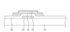
도 1 은 본 발명의 실시예에 따른 박막 트랜지스터 기판을 도시한 평면도이 고, 도 2는 도 1에 도시된 박막 트랜지스터 기판의 I-I'선을 따라 절단한 단면도이다.1 is a plan view illustrating a thin film transistor substrate according to an exemplary embodiment of the present invention, and FIG. 2 is a cross-sectional view taken along line II ′ of the thin film transistor substrate illustrated in FIG. 1.
도 1 및 도 2를 참조하면, 본 발명의 실시예에 따른 박막 트랜지스터 기판은, 기판(10), 게이트 라인(21), 데이터 라인(61), 화소 전극(90) 및 박막 트랜지스터(100)를 포함한다.1 and 2, a thin film transistor substrate according to an embodiment of the present invention may include a
구체적으로, 상기 기판(10)은 게이트 라인(21), 데이터 라인(61), 화소 전극(90) 및 박막 트랜지스터(100)가 형성되는 절연 기판으로서, 투명한 유리 또는 플라스틱 등의 재질로 형성되는 것이 바람직하다.Specifically, the
상기 게이트 라인(21)은 박막 트랜지스터(100)에 스캔 신호를 공급하고, 데이터 라인(61)은 박막 트랜지스터(100)에 화상 데이터 신호를 공급한다. 게이트 라인(21) 및 데이터 라인(61)은 게이트 절연막(30)을 사이에 두고 기판(100) 상에 교차하면서 형성되어 화소 영역을 정의한다. 화소 영역(90)에는 게이트 라인(21) 및 데이터 라인(61)과 접속되는 박막 트랜지스터(100), 박막 트랜지스터(100)에 연결되는 화소 전극(90)이 형성된다.The
상기 박막 트랜지스터(100)는 게이트 라인(21)으로부터 제공되는 스캔 신호에 응답하여 데이터 라인(61)으로부터 제공되는 화상 데이터 신호를 화소 전극(90)에 공급한다. 이를 위해 박막 트랜지스터(100)는 게이트 전극(20), 소스 전극(60), 드레인 전극(70), 반도체층(40) 및 오믹 콘택층(50)을 포함한다.The
게이트 전극(20)은 게이트 라인(21)과 접속되고, 소스 전극(60)은 데이터 라인(61)과 접속되고, 드레인 전극(70)은 화소 전극(90)에 접속된다. 반도체층(40) 은 드레인 전극(70) 및 게이트 전극(20)과 게이트 절연막(30)을 사이에 두고 중첩되도록 형성되어 소스 전극(60)과 드레인 전극(70) 사이에 채널을 형성한다.The
오믹 콘택층(50)은 소스 전극(60) 및 드레인 전극(70)과 반도체층(40) 사이의 오믹 접촉을 위한 것으로, 산화물 반도체로 형성되는 것이 바람직하다. 산화물 반도체는 대부분 n 타입으로 캐리어(Carrier) 농도가 종래 오믹 콘택층(50)을 구성하는, 불순물이 도핑된 비정질 실리콘(n+ a-Si:H)층보다 높기 때문에, 금속 재질의 소스 및 드레인 전극(60,70)과 아몰퍼스 실리콘 재질의 반도체층(40) 사이에서 좋은 콘택층의 역할을 수행할 수 있다. The
또한 산화물 반도체는 소스 및 드레인 전극(60,70)과 마찬가지로 습식 식각(Wet Etch)을 가능하게 하여 박막 트랜지스터 기판 제조 공정상 장점을 제공한다. 오믹 콘택층(50)을 산화물 반도체로 형성하는 경우 제공되는 제조 공정상 장점은 아래 박막 트랜지스터 기판의 제조 방법에서 좀 더 자세하게 설명한다.In addition, oxide semiconductors, like the source and drain
한편, 산화물 반도체는 산화 아연(ZnO) 및 첨가물이 부가된 산화 아연(ZnO)계 물질을 포함한다. 여기서 첨가물은 1족(H,Li,Na,K,Rb,Cs), 3족(Sc,Y,La), 5족(V,Nb,Ta,Db) 또는 7족(Mn,Tc,Re,Bh)의 원소일 수 있다.Meanwhile, the oxide semiconductor includes zinc oxide (ZnO) and a zinc oxide (ZnO) -based material to which an additive is added. Where the additive is Group 1 (H, Li, Na, K, Rb, Cs), Group 3 (Sc, Y, La), Group 5 (V, Nb, Ta, Db) or Group 7 (Mn, Tc, Re, It may be an element of Bh).
또한 산화물 반도체는 인듐 산화물(In2O3), 주석 산화물(SnO2) 또는 인듐 주석 산화물((In-Sn)Ox), 인듐 아연 산화물((In-Zn)Ox) 등의 비정질 산화물 반도체를 포함한다.The oxide semiconductor also includes amorphous oxide semiconductors such as indium oxide (In2 O3 ), tin oxide (SnO2 ) or indium tin oxide ((In-Sn) Ox), indium zinc oxide ((In-Zn) Ox), and the like. do.
상기 화소 전극(90)은 인듐 주석 산화물(Indium Tin Oxide; ITO) 또는 인듐 주석 산화물(Indium zinc Oxide; IZO) 등의 투명 도전성 금속 물질로 형성된다. 화소 전극(90)은 박막 트랜지스터(100)로부터 화상 데이터 신호가 공급되면, 공통 전압이 공급되는, 컬러 필터 기판(미도시)의 공통 전극과 함께 액정(미도시)을 구동하여 광투과율을 조절한다. 이를 위해 화소 전극(90)은 드레인 전극(70)을 노출시키며 박막 트랜지스터(100)를 덮는 보호막(80) 위에 형성되고, 콘택홀(95)을 통하여 드레인 전극(70)과 접속된다.The
도 3a 내지 도 3e는 본 발명의 제1 실시예에 따른 박막 트랜지스터 기판의 제조 방법을 순차적으로 도시한 단면도들로서, 5 마스크 공정을 통하여 박막 트랜지스터 기판을 제조하는 방법을 각 마스크 공정별로 도시한 단면도들이다.3A to 3E are cross-sectional views sequentially illustrating a method of manufacturing a thin film transistor substrate according to a first exemplary embodiment of the present invention. FIG. 3A to 3E are cross-sectional views illustrating a method of manufacturing a thin film transistor substrate using a five mask process for each mask process. .
먼저 도 3a는 본 발명의 제1 실시예에 따른 박막 트랜지스터 기판의 제조 방법 중 제1 마스크 공정을 도시한 단면도이다. 도 3a를 참조하면, 제1 마스크 공정은 제1 마스크를 통해 기판(10) 위에 제1 도전 패턴군이 형성되는 단계이다. 제1 도전 패턴군은 게이트 라인 및 게이트 전극(20)을 포함한다.3A is a cross-sectional view illustrating a first mask process in a method of manufacturing a thin film transistor substrate according to a first exemplary embodiment of the present invention. Referring to FIG. 3A, in the first mask process, a first conductive pattern group is formed on the
구체적으로, 기판(10) 위에 게이트 금속층이 스퍼터링(Sputtering)과 같은 증착 방법을 통해 형성된다. 여기서, 게이트 금속층은 알루미늄(Al), 크롬(Cr), 구리(Cu) 및 몰리브덴(Mo) 등과 같은 금속 또는 그들의 합금이 단일층으로 형성되거나, 그들의 조합으로 이루어진 다층 구조로 형성될 수 있다. 이어서, 제1 마스크를 이용한 포토리소그래피 공정과 식각 공정으로 게이트 금속층을 패터닝함으로써 게이트 라인 및 게이트 전극(20)을 포함하는 제1 도전 패턴군이 형성된다.Specifically, a gate metal layer is formed on the
도 3b는 본 발명의 제1 실시예에 따른 박막 트랜지스터 기판의 제조 방법 중 제2 마스크 공정을 도시한 단면도이다. 도 3b를 참조하면, 제2 마스크 공정은 제2 마스크를 통해, 제1 도전 패턴군이 형성된 기판(10) 상에 게이트 절연막(30), 반도체층(40) 및 오믹 콘택층(50)이 차례로 형성되는 단계이다.3B is a cross-sectional view illustrating a second mask process in the method of manufacturing the thin film transistor substrate according to the first embodiment of the present invention. Referring to FIG. 3B, in the second mask process, the
구체적으로, 게이트 라인 및 게이트 전극(20)이 형성된 기판(10) 상에 게이트 절연막(30), 비정질 실리콘층이 플라즈마 화학증착법(Plasma Enhanced Chemical Vapor Deposition; PECVD) 등의 증착 방법을 통해 형성된다. 여기서, 게이트 절연막(30)은 질화 실리콘(SiNx), 산화 실리콘(SiOx) 등의 무기 절연 물질일 수 있다. 그런 다음, 산화물 반도체층이 스퍼터링 방법을 통해 증착된다.In detail, the
이어서, 제2 마스크를 이용한 포토리소그래피 공정 및 식각 공정으로 비정질 실리콘층 및 산화물 반도체층이 패터닝됨으로써 반도체층(40) 및 오믹 콘택층(50)이 형성된다.Subsequently, the amorphous silicon layer and the oxide semiconductor layer are patterned by a photolithography process and an etching process using a second mask to form the
산화물 반도체는 도 1 및 도 2에서 설명한 바와 같이, 산화 아연(ZnO), 첨가물이 부가된 산화 아연(ZnO)계 물질, 결정질 산화물 반도체 또는 비정질 산화물 반도체를 포함한다.As described with reference to FIGS. 1 and 2, the oxide semiconductor includes zinc oxide (ZnO), a zinc oxide (ZnO) -based material to which an additive is added, a crystalline oxide semiconductor, or an amorphous oxide semiconductor.
도 3c는 본 발명의 제1 실시예에 따른 박막 트랜지스터 기판의 제조 방법 중 제3 마스크 공정을 도시한 단면도이다. 도 3c를 참조하면, 제3 마스크 공정은 제3 마스크를 통해, 반도체층(40) 및 오믹 콘택층(50)이 형성된 기판(10) 위에 제2 도전 패턴군이 형성되는 단계이다. 제2 도전 패턴군은 데이터 라인, 소스 전극(60) 및 드레인 전극(70)을 포함한다.3C is a cross-sectional view illustrating a third mask process in the method of manufacturing the thin film transistor substrate according to the first embodiment of the present invention. Referring to FIG. 3C, in the third mask process, a second conductive pattern group is formed on the
구체적으로, 게이트 절연막(30)과 오믹 콘택층(50) 상에 데이터 금속층을 스퍼터링 등의 증착 방법을 통해 증착한다. 여기서 데이터 금속층은 알루미늄(Al), 크롬(Cr), 구리(Cu) 및 몰리브덴(Mo) 등의 금속 또는 그들 합금의 단일층으로 형성되거나, 그들의 조합으로 이루어진 다층 구조일 수 있다.Specifically, the data metal layer is deposited on the
그리고 데이터 금속층을 패터닝하여 데이터 라인, 소스 및 드레인 전극(60,70)을 포함하는 제2 도전 패턴군을 형성한다. 이때 데이터 금속층 패터닝 방법은 산화물 반도체로 형성된 오믹 콘택층(50)을 동시에 패터닝 할 수 있는 습식 식각(Wet Etch)인 것이 바람직하다.The data metal layer is patterned to form a second conductive pattern group including data lines, source and drain
종래 공정에서는 데이터 금속층의 식각은 습식 식각(Wet Etch) 방식을 사용하고, 오믹 콘택층과 반도체층의 식각은 건식 식각(Dry Etch) 방식을 사용한다. 그러나 본발명의 일실시예에 따라 오믹 콘택층(50)을 산화물 반도체로 형성하는 경우 습식 식각 방법을 통하여 오믹 콘택층(50)은 데이터 금속층과 함께 패터닝될 수 있다.In the conventional process, the etching of the data metal layer uses a wet etching method, and the etching of the ohmic contact layer and the semiconductor layer uses a dry etching method. However, when the
한편 본 발명의 일실시예에 따른 습식 식각 방법에 사용되는 습식 식각액(Wet Etchant)은 식각 선택비(Etch Selectivity)가 큰 것이 바람직하다. 여기서 식각 선택비란 습식 식각액이 소스 및 드레인 전극(60,70)을 형성하는 데이터 금속층과 오믹 콘택층(50)을 형성하는 산화물 반도체를 식각시키는 반면 활성층을 형성하는 반도체층(40)은 식각시키지 않는 특성을 말한다.Meanwhile, the wet etchant used in the wet etching method according to an embodiment of the present invention preferably has a high etching selectivity. Here, the etching selectivity means that the wet etchant etches the data metal layer forming the source and drain
따라서 본 발명의 일실시예에 따르는 경우, 종래 두 번의 식각 공정(소스 및 드레인 전극 형성을 위한 습식 식각과 오믹 콘택층과 반도체층 식각을 위한 건식 식각 공정)을 한 번의 습식 식각 공정으로 대체할 수 있다.Therefore, according to an embodiment of the present invention, the conventional two etching processes (wet etching process for forming source and drain electrodes and dry etching process for ohmic contact layer and semiconductor layer etching) may be replaced with one wet etching process. have.
또한, 본 발명의 일실시예에 따르는 경우, 오믹 콘택층(50)을 구성하는 산화물 반도체는 습식 식각액에 식각되는 반면 활성층을 구성하는 반도체층(40)은 식각되지 않으므로 종래 백 채널 에치(BCE) 방법과는 달리, 활성층을 구성하는 반도체층(40)의 두께를 얇게 형성할 수 있도록 한다. 따라서, 본 발명의 일실시예에 따르는 경우, 포토 누설 전류(Photo Leakage Current)의 감소 및 전자 이동도(Extrinsic Field Effect Mobility)의 증가 등 박막 트랜지스터의 특성을 향상시킬 수 있다.In addition, according to the exemplary embodiment of the present invention, the oxide semiconductor constituting the
도 3d는 본 발명의 제1 실시예에 따른 박막 트랜지스터 기판의 제조 방법 중 제4 마스크 공정을 도시한 단면도이다. 도 3d를 참조하면, 제4 마스크 공정은 제4 마스크를 통해, 제2 도전 패턴군이 형성된 게이트 절연막(30) 위에 콘택홀(95)을 갖는 보호막(80)이 형성되는 단계이다.3D is a cross-sectional view illustrating a fourth mask process in the method of manufacturing the thin film transistor substrate according to the first embodiment of the present invention. Referring to FIG. 3D, in the fourth mask process, the
구체적으로, 보호막(80)은 제2 도전 패턴군이 형성된 기판(10) 상에 PECVD, 스핀 코팅 등의 증착 방법을 통해 형성되고, 제4 마스크를 이용한 포토리소그래피 공정 및 식각 공정으로 보호막(80)을 관통하여 드레인 전극(70)을 노출시키는 콘택홀(95)이 형성된다. 보호막(80)으로는 게이트 절연막(30)과 같은 무기 절연 물질 또는 유기 절연 물질이 이용된다.Specifically, the
도 3e는 본 발명의 제1 실시예에 따른 박막 트랜지스터 기판의 제조 방법 중 제5 마스크 공정을 도시한 단면도이다. 도 3e를 참조하면, 제5 마스크 공정은 제5 마스크를 통해 보호막(80) 위에 화소 전극(90)이 형성되는 단계이다.3E is a cross-sectional view illustrating a fifth mask process in the method of manufacturing the thin film transistor substrate according to the first embodiment of the present invention. Referring to FIG. 3E, in the fifth mask process, the
구체적으로, 화소 전극(90)은 보호막(80) 위에 스퍼터링 등의 방법을 통해 투명 도전층을 형성한 다음, 제5 마스크를 이용한 포토리소그래피 및 식각 공정으로 투명 도전층을 패터닝하여 형성된다. 투명 도전층으로는 인듐 주석 산화물(Indium Tin Oxide; ITO), 인듐 아연 산화물(Indium Zinc Oxide; IZO) 및 주석 산화물(Tin Oxide) 등과 같은 투명 도전 물질이 이용된다. 화소 전극(90)은 콘택홀(95)을 통해 드레인 전극(70)과 접속된다.Specifically, the
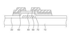
도 4a 내지 도 4e는 본 발명의 제2 실시예에 따른 박막 트랜지스터 기판의 제조 방법을 마스크 공정별로 도시한 단면도들로서, 4 마스크 공정을 통하여 박막 트랜지스터 기판을 제조하는 방법을 각 마스크 공정별로 도시한 단면도들이다.4A to 4E are cross-sectional views illustrating a method of manufacturing a thin film transistor substrate according to a second exemplary embodiment of the present invention, for each mask process, and a cross-sectional view illustrating a method of manufacturing a thin film transistor substrate through a four mask process for each mask process; admit.
먼저 도 4a는 본 발명의 제2 실시예에 따른 박막 트랜지스터 기판의 제조 방법 중 제1 마스크 공정을 도시한 단면도이다. 도 4a를 참조하면, 제1 마스크 공정은 제1 마스크를 통해, 기판(10) 위에 제1 도전 패턴군이 형성되는 단계이다. 제1 도전 패턴군은 게이트 라인 및 게이트 전극(20)을 포함한다.4A is a cross-sectional view illustrating a first mask process in a method of manufacturing a thin film transistor substrate according to a second exemplary embodiment of the present invention. Referring to FIG. 4A, in the first mask process, a first conductive pattern group is formed on the
구체적으로, 기판(10) 위에 게이트 금속층을 스퍼터링과 같은 증착 방법을 통해 형성된다. 여기서, 게이트 금속층은 알루미늄(Al), 크롬(Cr), 구리(Cu) 및 몰리브덴(Mo) 등과 같은 금속 또는 그들의 합금이 단일층으로 형성되거나, 그들의 조합으로 이루어진 다층 구조로 형성될 수 있다. 이어서, 제1 마스크를 이용한 포토리소그래피 공정과 식각 공정으로 게이트 금속층을 패터닝함으로써 게이트 라인 및 게이트 전극(20)을 포함하는 제1 도전 패턴군이 형성된다.Specifically, the gate metal layer is formed on the
도 4b 및 도 4c는 본 발명의 제2 실시예에 따른 박막 트랜지스터 기판의 제조 방법 중 제2 마스크 공정을 도시한 단면도이다. 도 4b 및 도 4c를 참조하면, 제2 마스크 공정은 제2 마스크를 통해, 게이트 금속층이 형성된 기판(10) 위에 게이트 절연막(30), 반도체층(40), 오믹 콘택층(50), 데이터 라인, 소스 전극(60) 및 드레인 전극(70)이 형성되는 단계이다.4B and 4C are cross-sectional views illustrating a second mask process in the method of manufacturing the thin film transistor substrate according to the second embodiment of the present invention. 4B and 4C, the second mask process may include a
구체적으로, 도 4b에 도시된 바와 같이 게이트 금속층이 형성된 기판(10) 상에 게이트 절연막(30), 비정질 실리콘층(140), 산화물 반도체층(150) 및 데이터 금속층(160)이 순차적으로 적층된다. 예를 들면, 게이트 절연막(30) 및 비정질 실리콘층(150)은 화학 기상 증착법(PECVD)으로 형성되고, 산화물 반도체층(150)은 및 데이터 금속층(160)은 스퍼터링 방법으로 형성된다. 게이트 절연막(30)은 산화 실리콘(SiOx), 질화 실리콘(SiNx) 등의 절연 물질로 형성된다. 산화물 반도체층(150)은 제1 실시예에서의 경우과 동일 물질이 적용된다. 데이터 금속층(160)은 몰리브덴(Mo), 티타늄(Ti), 구리(Cu), 알루미늄 나이트라이드(AlNd), 알루미늄(Al), 크롬(Cr), 몰리브덴(Mo)합금, 구리(Cu)합금, 알루미늄(Al)합금 등과 같은 금속 물질이 단일층 또는 이중층 이상의 적층된 형태로 형성될 수 있다.Specifically, as shown in FIG. 4B, the
그리고, 데이터 금속층(160) 위에 포토레지스트가 도포된 후, 슬릿 마스크를 이용한 포토리소그래피 공정으로 포토레지스트가 노광 및 형상됨으로써 포토레지스트 패턴을 형성한다.After the photoresist is applied on the
다음으로, 슬릿 마스크의 차단 영역은 반도체층(40)과 오믹 콘택층(50) 및 데이터 패턴이 형성될 영역에 위치하여 자외선을 차단함으로써 현상 후 포토레지스 트 패턴이 남게 되고, 슬릿 마스크의 슬릿 영역은 박막 트랜지스터의 채널이 형성될 영역에 위치하여 자외선을 회절시킴으로써 현상 후 포토레지스터가 제거되게 한다.Next, the blocking region of the slit mask is positioned in the region where the
이어서, 습식 식각 공정을 통해, 노출된 데이터 패턴과 그 아래의 오믹 콘택층(50)을 도 4c에 도시된 바와 같이 모두 제거한다. 데이터 금속층 및 산화물 반도체층은 동일 챔버 내에서 스퍼터링 방식에 의해 형성되므로 식각 공정 시 습식 식각에 의해 동시에 패터닝 된다. 따라서, 오믹 콘택층(50)의 식각 공정이 생략되어 마스크 수를 백 채널 에치(BCE) 방식에서와 동일한 수로 사용한다. 또한, 에치 스톱퍼(ES) 방식의 장점으로는 활성화층을 얇게 형성할 수 있는 점인데, 본실시예의 습식 식각액은 식각 선택비가 크기 때문에 반도체층(40)을 얇게 적용할 수 있게 된다.Then, the wet etching process removes both the exposed data pattern and the
도 4d는 본 발명의 제2 실시예에 따른 박막 트랜지스터 기판의 제조 방법 중 제3 마스크 공정을 도시한 단면도이다. 도 4d를 참조하면, 제3 마스크 공정은 제3 마스크를 통해 제2 도전 패턴군이 형성된 게이트 절연막(30) 위에 콘택홀(95)을 갖는 보호막(80)이 형성되는 단계이다.4D is a cross-sectional view illustrating a third mask process in the method of manufacturing the thin film transistor substrate according to the second embodiment of the present invention. Referring to FIG. 4D, in the third mask process, the
구체적으로, 보호막(80)은 제2 도전 패턴군이 형성된 기판 상에 PECVD, 스핀 코팅 등의 증착 방법을 통해 형성되고, 제3 마스크를 이용한 포토리소그래피 공정 및 식각 공정으로 보호막(80)을 관통하여 드레인 전극(70)을 노출시키는 콘택홀(95)이 형성된다. 보호막(80)으로는 게이트 절연막(30)과 같은 무기 절연 물질이 이용되거나, 유기 절연 물질이 이용된다.Specifically, the
도 4e는 본 발명의 제2 실시예에 따른 박막 트랜지스터 기판의 제조 방법 중 제4 마스크 공정을 도시한 단면도들이다. 도 4e를 참조하면, 제4 마스크 공정은 제4 마스크를 통해 보호막(80) 위에 화소 전극(90)이 형성되는 단게이다.4E are cross-sectional views illustrating a fourth mask process in the method of manufacturing the thin film transistor substrate according to the second embodiment of the present invention. Referring to FIG. 4E, in the fourth mask process, the
구체적으로, 화소 전극(90)은 보호막(80) 위에 스퍼터링 등의 방법을 통해 투명 도전층을 형성한 다음, 제4 마스크를 이용한 포토리소그래피 및 식각 공정으로 투명 도전층을 패터닝하여 형성한다. 투명 도전층으로는 인듐 주석 산화물(Indium Tin Oxide; ITO), 인듐 아연 산화물(Indium Zinc Oxide; IZO) 및 주석 산화물(Tin Oxide; TO) 등과 같은 투명 도전 물질이 이용된다. 화소 전극(90)은 콘택홀(95)을 통해 드레인 전극(70)과 접속된다.Specifically, the
상술한 바와 같이, 본 발명에 따른 박막 트랜지스터 기판 및 이의 제조 방법은 오믹 콘택층을 산화물 반도체로 형성하여 공정을 단순화하고 특성을 향상시킬 수 있다.As described above, the thin film transistor substrate and the manufacturing method thereof according to the present invention can simplify the process and improve the characteristics by forming the ohmic contact layer as an oxide semiconductor.
오믹 콘택층을 산화물 반도체로 형성하여, 백 채널 에치(BCE) 방식의 마스크 수를 줄일 수 있는 장점과 에치 스톱퍼(ES) 방식의 반도체층을 얇게 형성할 수 있는 장점을 동시에 얻을 수 있다.The ohmic contact layer may be formed of an oxide semiconductor to simultaneously reduce the number of back channel etch (BCE) masks and to form an etch stopper (ES) semiconductor layer.
이상에서 설명한 본 발명의 상세한 설명에서는 본 발명의 바람직한 실시 예를 참조하여 설명하였지만, 해당 기술 분야의 당업자 또는 해당 기술 분야에 통상의 지식을 갖는 자라면, 후술될 특허청구범위에 기재된 본 발명의 사상 및 기술 영 역으로부터 벗어나지 않는 범위 내에서 본 발명을 다양하게 수정 및 변경시킬 수 있음이 자명하다.Although the detailed description of the present invention described above has been described with reference to a preferred embodiment of the present invention, those skilled in the art or those skilled in the art, those skilled in the art will be described in the claims to be described later And various modifications and variations of the present invention can be made without departing from the technical scope.
Claims (24)
Translated fromKoreanPriority Applications (3)
| Application Number | Priority Date | Filing Date | Title |
|---|---|---|---|
| KR1020070037800AKR101325053B1 (en) | 2007-04-18 | 2007-04-18 | Thin film transistor substrate and manufacturing method thereof |
| US12/100,436US20080258143A1 (en) | 2007-04-18 | 2008-04-10 | Thin film transitor substrate and method of manufacturing the same |
| US12/961,170US20110183463A1 (en) | 2007-04-18 | 2010-12-06 | Thin film transitor substrate and method of manufacturing the same |
Applications Claiming Priority (1)
| Application Number | Priority Date | Filing Date | Title |
|---|---|---|---|
| KR1020070037800AKR101325053B1 (en) | 2007-04-18 | 2007-04-18 | Thin film transistor substrate and manufacturing method thereof |
Publications (2)
| Publication Number | Publication Date |
|---|---|
| KR20080093709A KR20080093709A (en) | 2008-10-22 |
| KR101325053B1true KR101325053B1 (en) | 2013-11-05 |
Family
ID=39871305
Family Applications (1)
| Application Number | Title | Priority Date | Filing Date |
|---|---|---|---|
| KR1020070037800AActiveKR101325053B1 (en) | 2007-04-18 | 2007-04-18 | Thin film transistor substrate and manufacturing method thereof |
Country Status (2)
| Country | Link |
|---|---|
| US (2) | US20080258143A1 (en) |
| KR (1) | KR101325053B1 (en) |
Families Citing this family (1827)
| Publication number | Priority date | Publication date | Assignee | Title |
|---|---|---|---|---|
| US7579224B2 (en)* | 2005-01-21 | 2009-08-25 | Semiconductor Energy Laboratory Co., Ltd. | Method for manufacturing a thin film semiconductor device |
| TWI445178B (en) | 2005-01-28 | 2014-07-11 | Semiconductor Energy Lab | Semiconductor device, electronic device, and method of manufacturing semiconductor device |
| TWI505473B (en) | 2005-01-28 | 2015-10-21 | Semiconductor Energy Lab | Semiconductor device, electronic device, and method of manufacturing semiconductor device |
| US7858451B2 (en)* | 2005-02-03 | 2010-12-28 | Semiconductor Energy Laboratory Co., Ltd. | Electronic device, semiconductor device and manufacturing method thereof |
| US7948171B2 (en) | 2005-02-18 | 2011-05-24 | Semiconductor Energy Laboratory Co., Ltd. | Light emitting device |
| US7928938B2 (en) | 2005-04-19 | 2011-04-19 | Semiconductor Energy Laboratory Co., Ltd. | Semiconductor device including memory circuit, display device and electronic apparatus |
| US8629819B2 (en) | 2005-07-14 | 2014-01-14 | Semiconductor Energy Laboratory Co., Ltd. | Semiconductor device and driving method thereof |
| EP1758072A3 (en)* | 2005-08-24 | 2007-05-02 | Semiconductor Energy Laboratory Co., Ltd. | Display device and driving method thereof |
| EP1770788A3 (en) | 2005-09-29 | 2011-09-21 | Semiconductor Energy Laboratory Co., Ltd. | Semiconductor device having oxide semiconductor layer and manufacturing method thereof |
| CN101577231B (en) | 2005-11-15 | 2013-01-02 | 株式会社半导体能源研究所 | Semiconductor device and method of manufacturing the same |
| EP1843194A1 (en) | 2006-04-06 | 2007-10-10 | Semiconductor Energy Laboratory Co., Ltd. | Liquid crystal display device, semiconductor device, and electronic appliance |
| JP5116277B2 (en) | 2006-09-29 | 2013-01-09 | 株式会社半導体エネルギー研究所 | Semiconductor device, display device, liquid crystal display device, display module, and electronic apparatus |
| US7646015B2 (en)* | 2006-10-31 | 2010-01-12 | Semiconductor Energy Laboratory Co., Ltd. | Manufacturing method of semiconductor device and semiconductor device |
| JP5542296B2 (en) | 2007-05-17 | 2014-07-09 | 株式会社半導体エネルギー研究所 | Liquid crystal display device, display module, and electronic device |
| JP5542297B2 (en) | 2007-05-17 | 2014-07-09 | 株式会社半導体エネルギー研究所 | Liquid crystal display device, display module, and electronic device |
| JP4989309B2 (en) | 2007-05-18 | 2012-08-01 | 株式会社半導体エネルギー研究所 | Liquid crystal display |
| US8354674B2 (en) | 2007-06-29 | 2013-01-15 | Semiconductor Energy Laboratory Co., Ltd. | Semiconductor device wherein a property of a first semiconductor layer is different from a property of a second semiconductor layer |
| WO2009014155A1 (en) | 2007-07-25 | 2009-01-29 | Semiconductor Energy Laboratory Co., Ltd. | Photoelectric conversion device and electronic device having the same |
| NO332409B1 (en)* | 2008-01-24 | 2012-09-17 | Well Technology As | Apparatus and method for isolating a section of a wellbore |
| US9041202B2 (en) | 2008-05-16 | 2015-05-26 | Semiconductor Energy Laboratory Co., Ltd. | Semiconductor device and manufacturing method of the same |
| US8314765B2 (en) | 2008-06-17 | 2012-11-20 | Semiconductor Energy Laboratory Co., Ltd. | Driver circuit, display device, and electronic device |
| KR100982314B1 (en)* | 2008-07-04 | 2010-09-15 | 삼성모바일디스플레이주식회사 | Thin film transistor, manufacturing method thereof and organic light emitting display device comprising same |
| KR101910451B1 (en) | 2008-07-10 | 2018-10-22 | 가부시키가이샤 한도오따이 에네루기 켄큐쇼 | Light-emitting device and electronic device using the same |
| JP2010056541A (en) | 2008-07-31 | 2010-03-11 | Semiconductor Energy Lab Co Ltd | Semiconductor device and manufacturing method thereof |
| TWI627757B (en) | 2008-07-31 | 2018-06-21 | 半導體能源研究所股份有限公司 | Semiconductor device |
| TWI469354B (en) | 2008-07-31 | 2015-01-11 | Semiconductor Energy Lab | Semiconductor device and method of manufacturing same |
| TWI491048B (en) | 2008-07-31 | 2015-07-01 | Semiconductor Energy Lab | Semiconductor device |
| JP5616038B2 (en) | 2008-07-31 | 2014-10-29 | 株式会社半導体エネルギー研究所 | Method for manufacturing semiconductor device |
| KR100975204B1 (en)* | 2008-08-04 | 2010-08-10 | 삼성모바일디스플레이주식회사 | Thin film transistor, its manufacturing method, and flat panel display device comprising thin film transistor |
| JP5525778B2 (en) | 2008-08-08 | 2014-06-18 | 株式会社半導体エネルギー研究所 | Semiconductor device |
| TWI508282B (en) | 2008-08-08 | 2015-11-11 | Semiconductor Energy Lab | Semiconductor device and method of manufacturing same |
| TWI424506B (en) | 2008-08-08 | 2014-01-21 | Semiconductor Energy Lab | Semiconductor device manufacturing method |
| JP5480554B2 (en) | 2008-08-08 | 2014-04-23 | 株式会社半導体エネルギー研究所 | Semiconductor device |
| JP5608347B2 (en)* | 2008-08-08 | 2014-10-15 | 株式会社半導体エネルギー研究所 | Semiconductor device and manufacturing method of semiconductor device |
| TWI511299B (en) | 2008-09-01 | 2015-12-01 | Semiconductor Energy Lab | Semiconductor device manufacturing method |
| US9082857B2 (en) | 2008-09-01 | 2015-07-14 | Semiconductor Energy Laboratory Co., Ltd. | Semiconductor device comprising an oxide semiconductor layer |
| JP5627071B2 (en) | 2008-09-01 | 2014-11-19 | 株式会社半導体エネルギー研究所 | Method for manufacturing semiconductor device |
| KR101657957B1 (en) | 2008-09-12 | 2016-09-20 | 가부시키가이샤 한도오따이 에네루기 켄큐쇼 | Display device |
| KR101767864B1 (en)* | 2008-09-12 | 2017-08-11 | 가부시키가이샤 한도오따이 에네루기 켄큐쇼 | Semiconductor device and manufacturing method thereof |
| KR101623224B1 (en) | 2008-09-12 | 2016-05-20 | 가부시키가이샤 한도오따이 에네루기 켄큐쇼 | Semiconductor device and method for manufacturing the same |
| WO2010029865A1 (en) | 2008-09-12 | 2010-03-18 | Semiconductor Energy Laboratory Co., Ltd. | Display device |
| KR101670695B1 (en) | 2008-09-19 | 2016-10-31 | 가부시키가이샤 한도오따이 에네루기 켄큐쇼 | Semiconductor device |
| CN102160103B (en) | 2008-09-19 | 2013-09-11 | 株式会社半导体能源研究所 | Display device |
| CN102160105B (en) | 2008-09-19 | 2014-06-11 | 株式会社半导体能源研究所 | Display device and manufacturing method thereof |
| KR101803264B1 (en) | 2008-09-19 | 2017-12-28 | 가부시키가이샤 한도오따이 에네루기 켄큐쇼 | Semiconductor device |
| CN102160184B (en) | 2008-09-19 | 2014-07-09 | 株式会社半导体能源研究所 | Display device |
| KR101611643B1 (en) | 2008-10-01 | 2016-04-11 | 가부시키가이샤 한도오따이 에네루기 켄큐쇼 | Semiconductor device |
| EP2172977A1 (en) | 2008-10-03 | 2010-04-07 | Semiconductor Energy Laboratory Co., Ltd. | Display device |
| EP2172804B1 (en) | 2008-10-03 | 2016-05-11 | Semiconductor Energy Laboratory Co, Ltd. | Display device |
| CN101714546B (en) | 2008-10-03 | 2014-05-14 | 株式会社半导体能源研究所 | Display device and manufacturing method thereof |
| KR101652693B1 (en) | 2008-10-03 | 2016-09-01 | 가부시키가이샤 한도오따이 에네루기 켄큐쇼 | Display device |
| KR101435501B1 (en) | 2008-10-03 | 2014-08-29 | 가부시키가이샤 한도오따이 에네루기 켄큐쇼 | Display device |
| CN101719493B (en) | 2008-10-08 | 2014-05-14 | 株式会社半导体能源研究所 | Display device |
| JP5484853B2 (en)* | 2008-10-10 | 2014-05-07 | 株式会社半導体エネルギー研究所 | Method for manufacturing semiconductor device |
| KR101799601B1 (en)* | 2008-10-16 | 2017-11-20 | 가부시키가이샤 한도오따이 에네루기 켄큐쇼 | Light-emitting display device |
| JP5361651B2 (en) | 2008-10-22 | 2013-12-04 | 株式会社半導体エネルギー研究所 | Method for manufacturing semiconductor device |
| US8741702B2 (en) | 2008-10-24 | 2014-06-03 | Semiconductor Energy Laboratory Co., Ltd. | Method for manufacturing semiconductor device |
| EP2180518B1 (en) | 2008-10-24 | 2018-04-25 | Semiconductor Energy Laboratory Co, Ltd. | Method for manufacturing semiconductor device |
| KR101667909B1 (en) | 2008-10-24 | 2016-10-28 | 가부시키가이샤 한도오따이 에네루기 켄큐쇼 | Method for manufacturing semiconductor device |
| KR20160072845A (en) | 2008-10-24 | 2016-06-23 | 가부시키가이샤 한도오따이 에네루기 켄큐쇼 | Semiconductor device and method for manufacturing the same |
| WO2010047288A1 (en) | 2008-10-24 | 2010-04-29 | Semiconductor Energy Laboratory Co., Ltd. | Method for manufacturing semiconductordevice |
| JP5616012B2 (en) | 2008-10-24 | 2014-10-29 | 株式会社半導体エネルギー研究所 | Method for manufacturing semiconductor device |
| JP5442234B2 (en) | 2008-10-24 | 2014-03-12 | 株式会社半導体エネルギー研究所 | Semiconductor device and display device |
| US8106400B2 (en) | 2008-10-24 | 2012-01-31 | Semiconductor Energy Laboratory Co., Ltd. | Semiconductor device and method for manufacturing the same |
| TWI567829B (en) | 2008-10-31 | 2017-01-21 | 半導體能源研究所股份有限公司 | Semiconductor device and method of manufacturing same |
| KR101603303B1 (en) | 2008-10-31 | 2016-03-14 | 가부시키가이샤 한도오따이 에네루기 켄큐쇼 | Conductive oxynitride and method for manufacturing conductive oxynitride film |
| WO2010050419A1 (en)* | 2008-10-31 | 2010-05-06 | Semiconductor Energy Laboratory Co., Ltd. | Driver circuit and display device |
| KR101631454B1 (en) | 2008-10-31 | 2016-06-17 | 가부시키가이샤 한도오따이 에네루기 켄큐쇼 | Logic circuit |
| KR20170021903A (en)* | 2008-11-07 | 2017-02-28 | 가부시키가이샤 한도오따이 에네루기 켄큐쇼 | Method of manufacturing a semiconductor device |
| EP2184783B1 (en) | 2008-11-07 | 2012-10-03 | Semiconductor Energy Laboratory Co, Ltd. | Semiconductor device and method for manufacturing the same |
| TWI467663B (en)* | 2008-11-07 | 2015-01-01 | Semiconductor Energy Lab | Semiconductor device and method of manufacturing the same |
| TWI487104B (en) | 2008-11-07 | 2015-06-01 | Semiconductor Energy Lab | Semiconductor device and method of manufacturing same |
| TWI606595B (en) | 2008-11-07 | 2017-11-21 | 半導體能源研究所股份有限公司 | Semiconductor device and method of manufacturing same |
| CN101740631B (en)* | 2008-11-07 | 2014-07-16 | 株式会社半导体能源研究所 | Semiconductor device and method for manufacturing the semiconductor device |
| TWI656645B (en) | 2008-11-13 | 2019-04-11 | 日商半導體能源研究所股份有限公司 | Semiconductor device and method of manufacturing same |
| KR101432764B1 (en) | 2008-11-13 | 2014-08-21 | 가부시키가이샤 한도오따이 에네루기 켄큐쇼 | Method for manufacturing semiconductor device |
| US8232947B2 (en) | 2008-11-14 | 2012-07-31 | Semiconductor Energy Laboratory Co., Ltd. | Liquid crystal display device |
| JP2010153802A (en)* | 2008-11-20 | 2010-07-08 | Semiconductor Energy Lab Co Ltd | Semiconductor device and method of manufacturing the same |
| KR101914404B1 (en)* | 2008-11-21 | 2018-11-01 | 가부시키가이샤 한도오따이 에네루기 켄큐쇼 | Semiconductor device |
| TWI749283B (en) | 2008-11-28 | 2021-12-11 | 日商半導體能源研究所股份有限公司 | Liquid crystal display device |
| TWI585955B (en) | 2008-11-28 | 2017-06-01 | 半導體能源研究所股份有限公司 | Light sensor and display device |
| TWI506795B (en) | 2008-11-28 | 2015-11-01 | Semiconductor Energy Lab | Semiconductor device and method of manufacturing same |
| KR101643204B1 (en) | 2008-12-01 | 2016-07-27 | 가부시키가이샤 한도오따이 에네루기 켄큐쇼 | Semiconductor device and manufacturing method thereof |
| TWI633371B (en) | 2008-12-03 | 2018-08-21 | 半導體能源研究所股份有限公司 | Liquid crystal display device |
| JP5491833B2 (en)* | 2008-12-05 | 2014-05-14 | 株式会社半導体エネルギー研究所 | Semiconductor device |
| WO2010071183A1 (en)* | 2008-12-19 | 2010-06-24 | Semiconductor Energy Laboratory Co., Ltd. | Method for manufacturing semiconductor device |
| CN103456794B (en) | 2008-12-19 | 2016-08-10 | 株式会社半导体能源研究所 | How Transistors Are Made |
| EP2515337B1 (en) | 2008-12-24 | 2016-02-24 | Semiconductor Energy Laboratory Co., Ltd. | Driver circuit and semiconductor device |
| KR20100075026A (en)* | 2008-12-24 | 2010-07-02 | 삼성전자주식회사 | Thin film transistor array substrate and method of fabricating the same |
| US8114720B2 (en) | 2008-12-25 | 2012-02-14 | Semiconductor Energy Laboratory Co., Ltd. | Semiconductor device and manufacturing method thereof |
| KR101719350B1 (en)* | 2008-12-25 | 2017-03-23 | 가부시키가이샤 한도오따이 에네루기 켄큐쇼 | Semiconductor device and manufacturing method thereof |
| US8383470B2 (en)* | 2008-12-25 | 2013-02-26 | Semiconductor Energy Laboratory Co., Ltd. | Thin film transistor (TFT) having a protective layer and manufacturing method thereof |
| US8441007B2 (en) | 2008-12-25 | 2013-05-14 | Semiconductor Energy Laboratory Co., Ltd. | Display device and manufacturing method thereof |
| JP5590877B2 (en)* | 2008-12-26 | 2014-09-17 | 株式会社半導体エネルギー研究所 | Semiconductor device |
| TWI501319B (en) | 2008-12-26 | 2015-09-21 | Semiconductor Energy Lab | Semiconductor device and manufacturing method thereof |
| KR101648927B1 (en) | 2009-01-16 | 2016-08-17 | 가부시키가이샤 한도오따이 에네루기 켄큐쇼 | Semiconductor device and manufacturing method thereof |
| US8492756B2 (en) | 2009-01-23 | 2013-07-23 | Semiconductor Energy Laboratory Co., Ltd. | Semiconductor device and method for manufacturing the same |
| US8436350B2 (en)* | 2009-01-30 | 2013-05-07 | Semiconductor Energy Laboratory Co., Ltd. | Semiconductor device using an oxide semiconductor with a plurality of metal clusters |
| US8367486B2 (en) | 2009-02-05 | 2013-02-05 | Semiconductor Energy Laboratory Co., Ltd. | Transistor and method for manufacturing the transistor |
| US8174021B2 (en)* | 2009-02-06 | 2012-05-08 | Semiconductor Energy Laboratory Co., Ltd. | Semiconductor device and method of manufacturing the semiconductor device |
| US8749930B2 (en)* | 2009-02-09 | 2014-06-10 | Semiconductor Energy Laboratory Co., Ltd. | Protection circuit, semiconductor device, photoelectric conversion device, and electronic device |
| US8278657B2 (en)* | 2009-02-13 | 2012-10-02 | Semiconductor Energy Laboratory Co., Ltd. | Transistor, semiconductor device including the transistor, and manufacturing method of the transistor and the semiconductor device |
| CN101840936B (en) | 2009-02-13 | 2014-10-08 | 株式会社半导体能源研究所 | Semiconductor device including a transistor, and manufacturing method of the semiconductor device |
| US8247812B2 (en) | 2009-02-13 | 2012-08-21 | Semiconductor Energy Laboratory Co., Ltd. | Transistor, semiconductor device including the transistor, and manufacturing method of the transistor and the semiconductor device |
| KR101593443B1 (en)* | 2009-02-19 | 2016-02-12 | 엘지디스플레이 주식회사 | Method of fabricating array substrate |
| US8247276B2 (en)* | 2009-02-20 | 2012-08-21 | Semiconductor Energy Laboratory Co., Ltd. | Thin film transistor, method for manufacturing the same, and semiconductor device |
| US8841661B2 (en) | 2009-02-25 | 2014-09-23 | Semiconductor Energy Laboratory Co., Ltd. | Staggered oxide semiconductor TFT semiconductor device and manufacturing method thereof |
| US8704216B2 (en) | 2009-02-27 | 2014-04-22 | Semiconductor Energy Laboratory Co., Ltd. | Semiconductor device and manufacturing method thereof |
| US20100224878A1 (en) | 2009-03-05 | 2010-09-09 | Semiconductor Energy Laboratory Co., Ltd. | Semiconductor device |
| US8461582B2 (en) | 2009-03-05 | 2013-06-11 | Semiconductor Energy Laboratory Co., Ltd. | Semiconductor device and method for manufacturing the same |
| JP5504008B2 (en) | 2009-03-06 | 2014-05-28 | 株式会社半導体エネルギー研究所 | Semiconductor device |
| KR102391280B1 (en) | 2009-03-12 | 2022-04-28 | 가부시키가이샤 한도오따이 에네루기 켄큐쇼 | Semiconductor device |
| TWI485781B (en) | 2009-03-13 | 2015-05-21 | Semiconductor Energy Lab | Semiconductor device and method of manufacturing the same |
| US8450144B2 (en)* | 2009-03-26 | 2013-05-28 | Semiconductor Energy Laboratory Co., Ltd. | Semiconductor device and method for manufacturing the same |
| KR101752640B1 (en) | 2009-03-27 | 2017-06-30 | 가부시키가이샤 한도오따이 에네루기 켄큐쇼 | Semiconductor device |
| KR101681884B1 (en) | 2009-03-27 | 2016-12-05 | 가부시키가이샤 한도오따이 에네루기 켄큐쇼 | Semiconductor device, display device, and electronic appliance |
| TWI511288B (en) | 2009-03-27 | 2015-12-01 | Semiconductor Energy Lab | Semiconductor device |
| US8927981B2 (en)* | 2009-03-30 | 2015-01-06 | Semiconductor Energy Laboratory Co., Ltd. | Semiconductor device and method for manufacturing the same |
| TWI489628B (en)* | 2009-04-02 | 2015-06-21 | Semiconductor Energy Lab | Semiconductor device and method of manufacturing same |
| US8338226B2 (en)* | 2009-04-02 | 2012-12-25 | Semiconductor Energy Laboratory Co., Ltd. | Method for manufacturing semiconductor device |
| JP5615018B2 (en) | 2009-04-10 | 2014-10-29 | 株式会社半導体エネルギー研究所 | Semiconductor device and manufacturing method of semiconductor device |
| TWI535023B (en) | 2009-04-16 | 2016-05-21 | 半導體能源研究所股份有限公司 | Semiconductor device and method of manufacturing same |
| JP5669426B2 (en)* | 2009-05-01 | 2015-02-12 | 株式会社半導体エネルギー研究所 | Method for manufacturing semiconductor device |
| JP5751762B2 (en) | 2009-05-21 | 2015-07-22 | 株式会社半導体エネルギー研究所 | Semiconductor device |
| KR101218090B1 (en)* | 2009-05-27 | 2013-01-18 | 엘지디스플레이 주식회사 | Oxide thin film transistor and method of fabricating the same |
| EP2256795B1 (en)* | 2009-05-29 | 2014-11-19 | Semiconductor Energy Laboratory Co., Ltd. | Manufacturing method for oxide semiconductor device |
| EP2256814B1 (en)* | 2009-05-29 | 2019-01-16 | Semiconductor Energy Laboratory Co, Ltd. | Oxide semiconductor device and method for manufacturing the same |
| JP5564331B2 (en) | 2009-05-29 | 2014-07-30 | 株式会社半導体エネルギー研究所 | Method for manufacturing semiconductor device |
| KR101287478B1 (en)* | 2009-06-02 | 2013-07-19 | 엘지디스플레이 주식회사 | Display device having oxide thin film transistor and method of fabricating thereof |
| JPWO2011001715A1 (en)* | 2009-06-29 | 2012-12-13 | シャープ株式会社 | Oxide semiconductor, thin film transistor array substrate, manufacturing method thereof, and display device |
| KR101810699B1 (en) | 2009-06-30 | 2018-01-25 | 가부시키가이샤 한도오따이 에네루기 켄큐쇼 | Method for manufacturing semiconductor device |
| WO2011001881A1 (en) | 2009-06-30 | 2011-01-06 | Semiconductor Energy Laboratory Co., Ltd. | Method for manufacturing semiconductor device |
| KR102011616B1 (en) | 2009-06-30 | 2019-08-16 | 가부시키가이샤 한도오따이 에네루기 켄큐쇼 | Method for manufacturing semiconductor device |
| KR101732859B1 (en) | 2009-06-30 | 2017-05-04 | 가부시키가이샤 한도오따이 에네루기 켄큐쇼 | Method for manufacturing semiconductor device |
| US20110000175A1 (en)* | 2009-07-01 | 2011-01-06 | Husqvarna Consumer Outdoor Products N.A. Inc. | Variable speed controller |
| KR101476817B1 (en) | 2009-07-03 | 2014-12-26 | 가부시키가이샤 한도오따이 에네루기 켄큐쇼 | Display device including transistor and manufacturing method thereof |
| KR102503687B1 (en) | 2009-07-03 | 2023-02-27 | 가부시키가이샤 한도오따이 에네루기 켄큐쇼 | Method for manufacturing semiconductor device |
| JP5663214B2 (en)* | 2009-07-03 | 2015-02-04 | 株式会社半導体エネルギー研究所 | Method for manufacturing semiconductor device |
| KR101857405B1 (en) | 2009-07-10 | 2018-05-11 | 가부시키가이샤 한도오따이 에네루기 켄큐쇼 | Semiconductor device and method for manufacturing the same |
| KR101791370B1 (en) | 2009-07-10 | 2017-10-27 | 가부시키가이샤 한도오따이 에네루기 켄큐쇼 | Semiconductor device |
| KR102798889B1 (en) | 2009-07-10 | 2025-04-23 | 가부시키가이샤 한도오따이 에네루기 켄큐쇼 | Method for manufacturing liquid crystal display device |
| WO2011007682A1 (en) | 2009-07-17 | 2011-01-20 | Semiconductor Energy Laboratory Co., Ltd. | Method of manufacturing semiconductor device |
| WO2011007677A1 (en) | 2009-07-17 | 2011-01-20 | Semiconductor Energy Laboratory Co., Ltd. | Semiconductor device and method for manufacturing the same |
| KR101739154B1 (en)* | 2009-07-17 | 2017-05-23 | 가부시키가이샤 한도오따이 에네루기 켄큐쇼 | Semiconductor device and manufacturing method thereof |
| WO2011010541A1 (en) | 2009-07-18 | 2011-01-27 | Semiconductor Energy Laboratory Co., Ltd. | Semiconductor device and method for manufacturing the same |
| WO2011010545A1 (en)* | 2009-07-18 | 2011-01-27 | Semiconductor Energy Laboratory Co., Ltd. | Semiconductor device and method for manufacturing the same |
| CN105070749B (en) | 2009-07-18 | 2019-08-09 | 株式会社半导体能源研究所 | Semiconductor device and method of manufacturing semiconductor device |
| CN102751295B (en) | 2009-07-18 | 2015-07-15 | 株式会社半导体能源研究所 | Semiconductor device and method for manufacturing semiconductor device |
| WO2011010542A1 (en) | 2009-07-23 | 2011-01-27 | Semiconductor Energy Laboratory Co., Ltd. | Semiconductor device and method for manufacturing the same |
| KR101904811B1 (en) | 2009-07-24 | 2018-10-05 | 가부시키가이샤 한도오따이 에네루기 켄큐쇼 | Semiconductor device |
| KR102097932B1 (en) | 2009-07-31 | 2020-04-06 | 가부시키가이샤 한도오따이 에네루기 켄큐쇼 | Semiconductor device and manufacturing method thereof |
| WO2011013502A1 (en)* | 2009-07-31 | 2011-02-03 | Semiconductor Energy Laboratory Co., Ltd. | Semiconductor device and manufacturing method thereof |
| KR101799252B1 (en) | 2009-07-31 | 2017-11-17 | 가부시키가이샤 한도오따이 에네루기 켄큐쇼 | Semiconductor device and method for manufacturing the same |
| WO2011013596A1 (en) | 2009-07-31 | 2011-02-03 | Semiconductor Energy Laboratory Co., Ltd. | Semiconductor device and manufacturing method thereof |
| WO2011013523A1 (en) | 2009-07-31 | 2011-02-03 | Semiconductor Energy Laboratory Co., Ltd. | Semiconductor device and method for manufacturing the same |
| TWI596741B (en) | 2009-08-07 | 2017-08-21 | 半導體能源研究所股份有限公司 | Semiconductor device and method of manufacturing same |
| TWI604594B (en)* | 2009-08-07 | 2017-11-01 | 半導體能源研究所股份有限公司 | Semiconductor device and telephone, watch, and display device including the same |
| TWI634642B (en) | 2009-08-07 | 2018-09-01 | 半導體能源研究所股份有限公司 | Semiconductor device and method of manufacturing same |
| JP5642447B2 (en) | 2009-08-07 | 2014-12-17 | 株式会社半導体エネルギー研究所 | Semiconductor device |
| EP2284891B1 (en) | 2009-08-07 | 2019-07-24 | Semiconductor Energy Laboratory Co, Ltd. | Semiconductor device and manufacturing method thereof |
| TWI700810B (en) | 2009-08-07 | 2020-08-01 | 日商半導體能源研究所股份有限公司 | Semiconductor device and method for manufacturing the same |
| JP5663231B2 (en) | 2009-08-07 | 2015-02-04 | 株式会社半導体エネルギー研究所 | Light emitting device |
| US8115883B2 (en)* | 2009-08-27 | 2012-02-14 | Semiconductor Energy Laboratory Co., Ltd. | Display device and method for manufacturing the same |
| WO2011027649A1 (en)* | 2009-09-02 | 2011-03-10 | Semiconductor Energy Laboratory Co., Ltd. | Semiconductor device including a transistor, and manufacturing method of semiconductor device |
| WO2011027656A1 (en) | 2009-09-04 | 2011-03-10 | Semiconductor Energy Laboratory Co., Ltd. | Transistor and display device |
| KR101746198B1 (en) | 2009-09-04 | 2017-06-12 | 가부시키가이샤 한도오따이 에네루기 켄큐쇼 | Display device and electronic device |
| WO2011027676A1 (en) | 2009-09-04 | 2011-03-10 | Semiconductor Energy Laboratory Co., Ltd. | Semiconductor device and manufacturing method thereof |
| WO2011027664A1 (en)* | 2009-09-04 | 2011-03-10 | Semiconductor Energy Laboratory Co., Ltd. | Liquid crystal display device and method for manufacturing the same |
| CN104681447A (en) | 2009-09-04 | 2015-06-03 | 株式会社半导体能源研究所 | Manufacturing Method Of Semiconductor Device |
| WO2011027702A1 (en) | 2009-09-04 | 2011-03-10 | Semiconductor Energy Laboratory Co., Ltd. | Light-emitting device and method for manufacturing the same |
| CN102598283B (en) | 2009-09-04 | 2016-05-18 | 株式会社半导体能源研究所 | Semiconductor device and manufacturing method thereof |
| WO2011027701A1 (en) | 2009-09-04 | 2011-03-10 | Semiconductor Energy Laboratory Co., Ltd. | Light-emitting device and method for manufacturing the same |
| US9805641B2 (en)* | 2009-09-04 | 2017-10-31 | Semiconductor Energy Laboratory Co., Ltd. | Display device and electronic device including the same |
| CN102498570B (en) | 2009-09-04 | 2016-02-10 | 株式会社半导体能源研究所 | Light emitting device and manufacturing method thereof |
| US9715845B2 (en) | 2009-09-16 | 2017-07-25 | Semiconductor Energy Laboratory Co., Ltd. | Semiconductor display device |
| KR20190045396A (en) | 2009-09-16 | 2019-05-02 | 가부시키가이샤 한도오따이 에네루기 켄큐쇼 | Transistor |
| KR101709749B1 (en) | 2009-09-16 | 2017-03-08 | 가부시키가이샤 한도오따이 에네루기 켄큐쇼 | Driving method of display device and display device |
| WO2011033909A1 (en)* | 2009-09-16 | 2011-03-24 | Semiconductor Energy Laboratory Co., Ltd. | Driver circuit, display device including the driver circuit, and electronic device including the display device |
| KR20230165355A (en) | 2009-09-16 | 2023-12-05 | 가부시키가이샤 한도오따이 에네루기 켄큐쇼 | Display device |
| WO2011034012A1 (en) | 2009-09-16 | 2011-03-24 | Semiconductor Energy Laboratory Co., Ltd. | Logic circuit, light emitting device, semiconductor device, and electronic device |
| CN102511082B (en)* | 2009-09-16 | 2016-04-27 | 株式会社半导体能源研究所 | Semiconductor device and manufacturing method thereof |
| KR20120068772A (en) | 2009-09-16 | 2012-06-27 | 가부시키가이샤 한도오따이 에네루기 켄큐쇼 | Light-emitting device and manufacturing method thereof |
| KR101628254B1 (en) | 2009-09-21 | 2016-06-09 | 삼성디스플레이 주식회사 | Thin film transistor array panel and method for manufacturing the same |
| CN105513644B (en) | 2009-09-24 | 2019-10-15 | 株式会社半导体能源研究所 | Driver circuit, display device including driver circuit, and electronic appliance including display device |
| TWI512997B (en) | 2009-09-24 | 2015-12-11 | Semiconductor Energy Lab | Semiconductor device, power supply circuit, and method of manufacturing semiconductor device |
| KR102219095B1 (en)* | 2009-09-24 | 2021-02-23 | 가부시키가이샤 한도오따이 에네루기 켄큐쇼 | Semiconductor device and method for manufacturing the same |
| WO2011037008A1 (en)* | 2009-09-24 | 2011-03-31 | Semiconductor Energy Laboratory Co., Ltd. | Method for manufacturing oxide semiconductor film and method for manufacturing semiconductor device |
| WO2011037050A1 (en) | 2009-09-24 | 2011-03-31 | Semiconductor Energy Laboratory Co., Ltd. | Semiconductor device and manufacturing method thereof |
| KR101707260B1 (en) | 2009-09-24 | 2017-02-15 | 가부시키가이샤 한도오따이 에네루기 켄큐쇼 | Semiconductor device |
| KR101740943B1 (en) | 2009-09-24 | 2017-06-15 | 가부시키가이샤 한도오따이 에네루기 켄큐쇼 | Display device |
| KR20220127372A (en) | 2009-09-24 | 2022-09-19 | 가부시키가이샤 한도오따이 에네루기 켄큐쇼 | Oxide semiconductor film and semiconductor device |
| WO2011037010A1 (en) | 2009-09-24 | 2011-03-31 | Semiconductor Energy Laboratory Co., Ltd. | Semiconductor element and method for manufacturing the same |
| WO2011040349A1 (en)* | 2009-09-30 | 2011-04-07 | Semiconductor Energy Laboratory Co., Ltd. | Redox capacitor and manufacturing method thereof |
| KR101767035B1 (en)* | 2009-10-01 | 2017-08-10 | 가부시키가이샤 한도오따이 에네루기 켄큐쇼 | Semiconductor device and method for manufacturing the same |
| WO2011043182A1 (en) | 2009-10-05 | 2011-04-14 | Semiconductor Energy Laboratory Co., Ltd. | Method for removing electricity and method for manufacturing semiconductor device |
| KR20120084751A (en) | 2009-10-05 | 2012-07-30 | 가부시키가이샤 한도오따이 에네루기 켄큐쇼 | Semiconductor device and manufacturing method thereof |
| EP2486594B1 (en) | 2009-10-08 | 2017-10-25 | Semiconductor Energy Laboratory Co., Ltd. | Oxide semiconductor device |
| KR102246127B1 (en) | 2009-10-08 | 2021-04-29 | 가부시키가이샤 한도오따이 에네루기 켄큐쇼 | Semiconductor device |
| KR101396096B1 (en) | 2009-10-09 | 2014-05-15 | 가부시키가이샤 한도오따이 에네루기 켄큐쇼 | Semiconductor device and manufacturing method thereof |
| KR102329380B1 (en) | 2009-10-09 | 2021-11-22 | 가부시키가이샤 한도오따이 에네루기 켄큐쇼 | Semiconductor device |
| KR101424950B1 (en)* | 2009-10-09 | 2014-08-01 | 가부시키가이샤 한도오따이 에네루기 켄큐쇼 | Liquid crystal display device |
| KR101882350B1 (en) | 2009-10-09 | 2018-07-27 | 가부시키가이샤 한도오따이 에네루기 켄큐쇼 | Display device |
| KR101820973B1 (en)* | 2009-10-09 | 2018-01-22 | 가부시키가이샤 한도오따이 에네루기 켄큐쇼 | Semiconductor device and method for manufacturing the semiconductor device |
| WO2011043164A1 (en)* | 2009-10-09 | 2011-04-14 | Semiconductor Energy Laboratory Co., Ltd. | Semiconductor device and method for manufacturing the semiconductor device |
| KR101759504B1 (en) | 2009-10-09 | 2017-07-19 | 가부시키가이샤 한도오따이 에네루기 켄큐쇼 | Light-emitting display device and electronic device including the same |
| CN102598278B (en)* | 2009-10-09 | 2015-04-08 | 株式会社半导体能源研究所 | Semiconductor device |
| WO2011043206A1 (en) | 2009-10-09 | 2011-04-14 | Semiconductor Energy Laboratory Co., Ltd. | Semiconductor device |
| KR101843558B1 (en) | 2009-10-09 | 2018-03-30 | 가부시키가이샤 한도오따이 에네루기 켄큐쇼 | Shift register and display device and driving method thereof |
| WO2011043194A1 (en) | 2009-10-09 | 2011-04-14 | Semiconductor Energy Laboratory Co., Ltd. | Semiconductor device and method for manufacturing the same |
| KR101779349B1 (en) | 2009-10-14 | 2017-09-18 | 가부시키가이샤 한도오따이 에네루기 켄큐쇼 | Semiconductor device and manufacturing method thereof |
| KR101717460B1 (en) | 2009-10-16 | 2017-03-17 | 가부시키가이샤 한도오따이 에네루기 켄큐쇼 | Liquid crystal display device and electronic device including the liquid crystal display device |
| KR102143040B1 (en) | 2009-10-16 | 2020-08-11 | 가부시키가이샤 한도오따이 에네루기 켄큐쇼 | Liquid crystal display device and electronic apparatus having the same |
| KR101772639B1 (en)* | 2009-10-16 | 2017-08-29 | 가부시키가이샤 한도오따이 에네루기 켄큐쇼 | Semiconductor device |
| KR102462043B1 (en) | 2009-10-16 | 2022-11-03 | 가부시키가이샤 한도오따이 에네루기 켄큐쇼 | Semiconductor device |
| KR101745747B1 (en) | 2009-10-16 | 2017-06-27 | 가부시키가이샤 한도오따이 에네루기 켄큐쇼 | Logic circuit and semiconductor device |
| CN105702688B (en) | 2009-10-21 | 2020-09-08 | 株式会社半导体能源研究所 | Liquid crystal display device and electronic apparatus including the same |
| CN107731931B (en) | 2009-10-21 | 2021-03-23 | 株式会社半导体能源研究所 | Display device and electronic equipment including display device |
| KR101490726B1 (en) | 2009-10-21 | 2015-02-09 | 가부시키가이샤 한도오따이 에네루기 켄큐쇼 | Semiconductor device |
| WO2011048923A1 (en) | 2009-10-21 | 2011-04-28 | Semiconductor Energy Laboratory Co., Ltd. | E-book reader |
| KR101751908B1 (en) | 2009-10-21 | 2017-06-28 | 가부시키가이샤 한도오따이 에네루기 켄큐쇼 | Voltage regulator circuit |
| KR101812683B1 (en) | 2009-10-21 | 2017-12-27 | 가부시키가이샤 한도오따이 에네루기 켄큐쇼 | Method for manufacturing semiconductor device |
| KR102162746B1 (en) | 2009-10-21 | 2020-10-07 | 가부시키가이샤 한도오따이 에네루기 켄큐쇼 | Analog circuit and semiconductor device |
| KR101291488B1 (en) | 2009-10-21 | 2013-07-31 | 가부시키가이샤 한도오따이 에네루기 켄큐쇼 | Semiconductor device |
| TWI467770B (en)* | 2009-10-26 | 2015-01-01 | Prime View Int Co Ltd | Display and its thin film transistor array substrate and thin film transistor |
| SG10201406869QA (en) | 2009-10-29 | 2014-12-30 | Semiconductor Energy Lab | Semiconductor device |
| KR101969279B1 (en) | 2009-10-29 | 2019-04-15 | 가부시키가이샤 한도오따이 에네루기 켄큐쇼 | Semiconductor device |
| CN102576708B (en) | 2009-10-30 | 2015-09-23 | 株式会社半导体能源研究所 | Semiconductor device |
| WO2011052411A1 (en)* | 2009-10-30 | 2011-05-05 | Semiconductor Energy Laboratory Co., Ltd. | Transistor |
| KR102019239B1 (en) | 2009-10-30 | 2019-09-06 | 가부시키가이샤 한도오따이 에네루기 켄큐쇼 | Semiconductor device |
| WO2011052382A1 (en) | 2009-10-30 | 2011-05-05 | Semiconductor Energy Laboratory Co., Ltd. | Semiconductor device and method for manufacturing the same |
| WO2011052367A1 (en) | 2009-10-30 | 2011-05-05 | Semiconductor Energy Laboratory Co., Ltd. | Semiconductor device |
| KR20120099657A (en)* | 2009-10-30 | 2012-09-11 | 가부시키가이샤 한도오따이 에네루기 켄큐쇼 | transistor |
| WO2011052366A1 (en) | 2009-10-30 | 2011-05-05 | Semiconductor Energy Laboratory Co., Ltd. | Voltage regulator circuit |
| WO2011052384A1 (en) | 2009-10-30 | 2011-05-05 | Semiconductor Energy Laboratory Co., Ltd. | Semiconductor device and method for manufacturing the same |
| KR101835155B1 (en)* | 2009-10-30 | 2018-03-06 | 가부시키가이샤 한도오따이 에네루기 켄큐쇼 | Liquid crystal display device, driving method of the same, and electronic appliance including the same |
| WO2011052368A1 (en) | 2009-10-30 | 2011-05-05 | Semiconductor Energy Laboratory Co., Ltd. | Driver circuit, display device including the driver circuit, and electronic device including the display device |
| WO2011052413A1 (en) | 2009-10-30 | 2011-05-05 | Semiconductor Energy Laboratory Co., Ltd. | Non-linear element, display device, and electronic device |
| WO2011052437A1 (en) | 2009-10-30 | 2011-05-05 | Semiconductor Energy Laboratory Co., Ltd. | Non-linear element, display device including non-linear element, and electronic device including display device |
| WO2011052410A1 (en)* | 2009-10-30 | 2011-05-05 | Semiconductor Energy Laboratory Co., Ltd. | Power diode, rectifier, and semiconductor device including the same |
| CN102687400B (en) | 2009-10-30 | 2016-08-24 | 株式会社半导体能源研究所 | Logic circuit and semiconductor device |
| WO2011055660A1 (en) | 2009-11-06 | 2011-05-12 | Semiconductor Energy Laboratory Co., Ltd. | Semiconductor device |
| KR101747158B1 (en) | 2009-11-06 | 2017-06-14 | 가부시키가이샤 한도오따이 에네루기 켄큐쇼 | Method for manufacturing semiconductor device |
| KR101753927B1 (en) | 2009-11-06 | 2017-07-04 | 가부시키가이샤 한도오따이 에네루기 켄큐쇼 | Semiconductor device |
| KR101488521B1 (en) | 2009-11-06 | 2015-02-02 | 가부시키가이샤 한도오따이 에네루기 켄큐쇼 | Semiconductor device |
| KR102148664B1 (en) | 2009-11-06 | 2020-08-28 | 가부시키가이샤 한도오따이 에네루기 켄큐쇼 | Semiconductor device and manufacturing method thereof |
| CN102598279B (en)* | 2009-11-06 | 2015-10-07 | 株式会社半导体能源研究所 | Semiconductor device |
| JP5539846B2 (en) | 2009-11-06 | 2014-07-02 | 株式会社半導体エネルギー研究所 | Evaluation method, manufacturing method of semiconductor device |
| KR101849321B1 (en) | 2009-11-06 | 2018-04-16 | 가부시키가이샤 한도오따이 에네루기 켄큐쇼 | Semiconductor device and manufacturing method thereof |
| KR101727469B1 (en) | 2009-11-06 | 2017-04-17 | 가부시키가이샤 한도오따이 에네루기 켄큐쇼 | Display device |
| WO2011055625A1 (en) | 2009-11-06 | 2011-05-12 | Semiconductor Energy Laboratory Co., Ltd. | Semiconductor device and operating method thereof |
| KR20120093952A (en)* | 2009-11-06 | 2012-08-23 | 가부시키가이샤 한도오따이 에네루기 켄큐쇼 | Method for manufacturing semiconductor element and semiconductor device, and deposition apparatus |
| CN102598284B (en) | 2009-11-06 | 2015-04-15 | 株式会社半导体能源研究所 | Semiconductor device |
| WO2011058913A1 (en)* | 2009-11-13 | 2011-05-19 | Semiconductor Energy Laboratory Co., Ltd. | Semiconductor device and manufacturing method thereof |
| KR102393447B1 (en) | 2009-11-13 | 2022-05-03 | 가부시키가이샤 한도오따이 에네루기 켄큐쇼 | Semiconductor device and manufacturing method thereof |
| KR102329497B1 (en) | 2009-11-13 | 2021-11-22 | 가부시키가이샤 한도오따이 에네루기 켄큐쇼 | Display device and electronic device including the same |
| KR101893332B1 (en) | 2009-11-13 | 2018-08-31 | 가부시키가이샤 한도오따이 에네루기 켄큐쇼 | Semiconductor device and driving method thereof |
| KR20120094013A (en) | 2009-11-13 | 2012-08-23 | 가부시키가이샤 한도오따이 에네루기 켄큐쇼 | Sputtering target and manufacturing method thereof, and transistor |
| CN102668097B (en)* | 2009-11-13 | 2015-08-12 | 株式会社半导体能源研究所 | Semiconductor device and manufacture method thereof |
| KR101738996B1 (en)* | 2009-11-13 | 2017-05-23 | 가부시키가이샤 한도오따이 에네루기 켄큐쇼 | Device including nonvolatile memory element |
| KR101721850B1 (en) | 2009-11-13 | 2017-03-31 | 가부시키가이샤 한도오따이 에네루기 켄큐쇼 | Semiconductor device |
| KR101975741B1 (en)* | 2009-11-13 | 2019-05-09 | 가부시키가이샤 한도오따이 에네루기 켄큐쇼 | Method for packaging target material and method for mounting target |
| WO2011062029A1 (en) | 2009-11-18 | 2011-05-26 | Semiconductor Energy Laboratory Co., Ltd. | Memory device |
| JP5762723B2 (en) | 2009-11-20 | 2015-08-12 | 株式会社半導体エネルギー研究所 | Modulation circuit and semiconductor device having the same |
| KR101370301B1 (en) | 2009-11-20 | 2014-03-05 | 가부시키가이샤 한도오따이 에네루기 켄큐쇼 | Method for manufacturing semiconductor device |
| CN104332177B (en) | 2009-11-20 | 2018-05-08 | 株式会社半导体能源研究所 | Non-volatile latch circuit and logic circuit, and use its semiconductor devices |
| KR101800852B1 (en) | 2009-11-20 | 2017-12-20 | 가부시키가이샤 한도오따이 에네루기 켄큐쇼 | Semiconductor device |
| KR20190124813A (en) | 2009-11-20 | 2019-11-05 | 가부시키가이샤 한도오따이 에네루기 켄큐쇼 | Semiconductor device |
| KR101945660B1 (en) | 2009-11-20 | 2019-02-07 | 가부시키가이샤 한도오따이 에네루기 켄큐쇼 | Transistor |
| WO2011062041A1 (en)* | 2009-11-20 | 2011-05-26 | Semiconductor Energy Laboratory Co., Ltd. | Transistor |
| KR101829176B1 (en) | 2009-11-20 | 2018-02-13 | 가부시키가이샤 한도오따이 에네루기 켄큐쇼 | Semiconductor device |
| WO2011062068A1 (en)* | 2009-11-20 | 2011-05-26 | Semiconductor Energy Laboratory Co., Ltd. | Semiconductor device |
| KR101448908B1 (en)* | 2009-11-20 | 2014-10-15 | 가부시키가이샤 한도오따이 에네루기 켄큐쇼 | Semiconductor device |
| KR101280827B1 (en)* | 2009-11-20 | 2013-07-02 | 엘지디스플레이 주식회사 | Array substrate and method of fabricating the same |
| WO2011065183A1 (en)* | 2009-11-24 | 2011-06-03 | Semiconductor Energy Laboratory Co., Ltd. | Semiconductor device including memory cell |
| WO2011065258A1 (en)* | 2009-11-27 | 2011-06-03 | Semiconductor Energy Laboratory Co., Ltd. | Semiconductor device |
| WO2011065209A1 (en)* | 2009-11-27 | 2011-06-03 | Semiconductor Energy Laboratory Co., Ltd. | Non-linear element, display device including non-linear element, and electronic device including display device |
| KR20170091760A (en) | 2009-11-27 | 2017-08-09 | 가부시키가이샤 한도오따이 에네루기 켄큐쇼 | Semiconductor device |
| KR101802406B1 (en)* | 2009-11-27 | 2017-11-28 | 가부시키가이샤 한도오따이 에네루기 켄큐쇼 | Semiconductor device and method for manufacturing the same |
| KR101825345B1 (en) | 2009-11-28 | 2018-02-05 | 가부시키가이샤 한도오따이 에네루기 켄큐쇼 | Stacked oxide material, semiconductor device, and method for manufacturing the semiconductor device |
| WO2011065244A1 (en) | 2009-11-28 | 2011-06-03 | Semiconductor Energy Laboratory Co., Ltd. | Semiconductor device and method for manufacturing the same |
| WO2011065243A1 (en) | 2009-11-28 | 2011-06-03 | Semiconductor Energy Laboratory Co., Ltd. | Semiconductor device and manufacturing method thereof |
| WO2011065210A1 (en) | 2009-11-28 | 2011-06-03 | Semiconductor Energy Laboratory Co., Ltd. | Stacked oxide material, semiconductor device, and method for manufacturing the semiconductor device |
| KR20110060479A (en) | 2009-11-30 | 2011-06-08 | 삼성모바일디스플레이주식회사 | A thin film transistor having an oxide semiconductor layer as an ohmic contact layer and a method of manufacturing the same |
| KR20180030255A (en) | 2009-11-30 | 2018-03-21 | 가부시키가이샤 한도오따이 에네루기 켄큐쇼 | Liquid crystal display device, method for driving the same, and electronic device including the same |
| WO2011068028A1 (en) | 2009-12-04 | 2011-06-09 | Semiconductor Energy Laboratory Co., Ltd. | Semiconductor element, semiconductor device, and method for manufacturing the same |
| KR102719739B1 (en) | 2009-12-04 | 2024-10-21 | 가부시키가이샤 한도오따이 에네루기 켄큐쇼 | Semiconductor device |
| JP2011139052A (en)* | 2009-12-04 | 2011-07-14 | Semiconductor Energy Lab Co Ltd | Semiconductor memory device |
| WO2011068022A1 (en) | 2009-12-04 | 2011-06-09 | Semiconductor Energy Laboratory Co., Ltd. | Semiconductor device |
| KR102250803B1 (en) | 2009-12-04 | 2021-05-11 | 가부시키가이샤 한도오따이 에네루기 켄큐쇼 | Semiconductor device |
| KR101797253B1 (en) | 2009-12-04 | 2017-11-13 | 가부시키가이샤 한도오따이 에네루기 켄큐쇼 | Semiconductor device and manufacturing method thereof |
| WO2011068025A1 (en) | 2009-12-04 | 2011-06-09 | Semiconductor Energy Laboratory Co., Ltd. | Dc converter circuit and power supply circuit |
| KR102241766B1 (en) | 2009-12-04 | 2021-04-19 | 가부시키가이샤 한도오따이 에네루기 켄큐쇼 | Semiconductor device and manufacturing method thereof |
| JP5584103B2 (en) | 2009-12-04 | 2014-09-03 | 株式会社半導体エネルギー研究所 | Semiconductor device |
| KR101523358B1 (en) | 2009-12-04 | 2015-05-27 | 가부시키가이샤 한도오따이 에네루기 켄큐쇼 | Display device |
| KR20120103676A (en)* | 2009-12-04 | 2012-09-19 | 가부시키가이샤 한도오따이 에네루기 켄큐쇼 | Semiconductor device |
| KR101840623B1 (en)* | 2009-12-04 | 2018-03-21 | 가부시키가이샤 한도오따이 에네루기 켄큐쇼 | Display device and electronic device including the same |
| KR101800038B1 (en) | 2009-12-04 | 2017-11-21 | 가부시키가이샤 한도오따이 에네루기 켄큐쇼 | Display device |
| KR101511076B1 (en)* | 2009-12-08 | 2015-04-10 | 가부시키가이샤 한도오따이 에네루기 켄큐쇼 | Semiconductor device and manufacturing method thereof |
| KR101945171B1 (en) | 2009-12-08 | 2019-02-07 | 가부시키가이샤 한도오따이 에네루기 켄큐쇼 | Semiconductor device |
| KR20170061194A (en) | 2009-12-10 | 2017-06-02 | 가부시키가이샤 한도오따이 에네루기 켄큐쇼 | Display device and driving method thereof |
| KR20120102748A (en) | 2009-12-11 | 2012-09-18 | 가부시키가이샤 한도오따이 에네루기 켄큐쇼 | Field effect transistor |
| WO2011070929A1 (en) | 2009-12-11 | 2011-06-16 | Semiconductor Energy Laboratory Co., Ltd. | Semiconductor device and electronic device |
| JP5727204B2 (en) | 2009-12-11 | 2015-06-03 | 株式会社半導体エネルギー研究所 | Method for manufacturing semiconductor device |
| KR101720072B1 (en) | 2009-12-11 | 2017-03-27 | 가부시키가이샤 한도오따이 에네루기 켄큐쇼 | Nonvolatile latch circuit and logic circuit, and semiconductor device using the same |
| WO2011070901A1 (en) | 2009-12-11 | 2011-06-16 | Semiconductor Energy Laboratory Co., Ltd. | Semiconductor device and manufacturing method thereof |
| KR101894821B1 (en) | 2009-12-11 | 2018-09-05 | 가부시키가이샤 한도오따이 에네루기 켄큐쇼 | Semiconductor device |
| WO2011074590A1 (en)* | 2009-12-17 | 2011-06-23 | Semiconductor Energy Laboratory Co., Ltd. | Semiconductor device, measurement apparatus, and measurement method of relative permittivity |
| KR102352590B1 (en) | 2009-12-18 | 2022-01-17 | 가부시키가이샤 한도오따이 에네루기 켄큐쇼 | Liquid crystal display device and electronic device |
| KR102257564B1 (en) | 2009-12-18 | 2021-05-31 | 가부시키가이샤 한도오따이 에네루기 켄큐쇼 | Driving method of display device and display device |
| KR101481399B1 (en) | 2009-12-18 | 2015-01-14 | 가부시키가이샤 한도오따이 에네루기 켄큐쇼 | Semiconductor device |
| KR101763660B1 (en) | 2009-12-18 | 2017-08-01 | 가부시키가이샤 한도오따이 에네루기 켄큐쇼 | Liquid crystal display device and driving method thereof |
| KR102020739B1 (en) | 2009-12-18 | 2019-09-10 | 가부시키가이샤 한도오따이 에네루기 켄큐쇼 | Display device including optical sensor and driving method thereof |
| WO2011074408A1 (en)* | 2009-12-18 | 2011-06-23 | Semiconductor Energy Laboratory Co., Ltd. | Non-volatile latch circuit and logic circuit, and semiconductor device using the same |
| KR101768433B1 (en) | 2009-12-18 | 2017-08-16 | 가부시키가이샤 한도오따이 에네루기 켄큐쇼 | Method for manufacturing semiconductor device |
| US9057758B2 (en) | 2009-12-18 | 2015-06-16 | Semiconductor Energy Laboratory Co., Ltd. | Method for measuring current, method for inspecting semiconductor device, semiconductor device, and test element group |
| WO2011074407A1 (en) | 2009-12-18 | 2011-06-23 | Semiconductor Energy Laboratory Co., Ltd. | Semiconductor device and method for manufacturing the same |
| WO2011077908A1 (en) | 2009-12-23 | 2011-06-30 | Semiconductor Energy Laboratory Co., Ltd. | Semiconductor device |
| KR20120101716A (en) | 2009-12-24 | 2012-09-14 | 가부시키가이샤 한도오따이 에네루기 켄큐쇼 | Display device and electronic device |
| WO2011077916A1 (en) | 2009-12-24 | 2011-06-30 | Semiconductor Energy Laboratory Co., Ltd. | Display device |
| CN103985760B (en) | 2009-12-25 | 2017-07-18 | 株式会社半导体能源研究所 | Semiconductor device |
| CN102656801B (en) | 2009-12-25 | 2016-04-27 | 株式会社半导体能源研究所 | Memory device, semiconductor device and electronic device |
| KR102111309B1 (en)* | 2009-12-25 | 2020-05-15 | 가부시키가이샤 한도오따이 에네루기 켄큐쇼 | Method for manufacturing semiconductor device |
| US8441009B2 (en)* | 2009-12-25 | 2013-05-14 | Semiconductor Energy Laboratory Co., Ltd. | Semiconductor device and manufacturing method thereof |
| KR20250048807A (en) | 2009-12-25 | 2025-04-10 | 가부시키가이샤 한도오따이 에네루기 켄큐쇼 | Semiconductor device |
| KR101613701B1 (en) | 2009-12-25 | 2016-04-19 | 가부시키가이샤 한도오따이 에네루기 켄큐쇼 | Method for driving liquid crystal display device |
| WO2011077978A1 (en) | 2009-12-25 | 2011-06-30 | Semiconductor Energy Laboratory Co., Ltd. | Method for manufacturing display device |
| CN105353551A (en) | 2009-12-28 | 2016-02-24 | 株式会社半导体能源研究所 | Liquid crystal display device and electronic device |
| WO2011081041A1 (en) | 2009-12-28 | 2011-07-07 | Semiconductor Energy Laboratory Co., Ltd. | Semiconductor device and method for manufacturing the semiconductor device |
| CN102903758B (en)* | 2009-12-28 | 2015-06-03 | 株式会社半导体能源研究所 | Semiconductor device |
| KR102198144B1 (en) | 2009-12-28 | 2021-01-04 | 가부시키가이샤 한도오따이 에네루기 켄큐쇼 | Memory device and semiconductor device |
| KR101762316B1 (en) | 2009-12-28 | 2017-07-27 | 가부시키가이샤 한도오따이 에네루기 켄큐쇼 | Semiconductor device |
| EP2519969A4 (en) | 2009-12-28 | 2016-07-06 | Semiconductor Energy Lab | SEMICONDUCTOR DEVICE |
| US8759917B2 (en)* | 2010-01-04 | 2014-06-24 | Samsung Electronics Co., Ltd. | Thin-film transistor having etch stop multi-layer and method of manufacturing the same |
| CN102725841B (en) | 2010-01-15 | 2016-10-05 | 株式会社半导体能源研究所 | Semiconductor devices |
| CN102696064B (en)* | 2010-01-15 | 2015-11-25 | 株式会社半导体能源研究所 | Semiconductor device and electronic installation |
| US8780629B2 (en)* | 2010-01-15 | 2014-07-15 | Semiconductor Energy Laboratory Co., Ltd. | Semiconductor device and driving method thereof |
| KR101791279B1 (en)* | 2010-01-15 | 2017-10-27 | 가부시키가이샤 한도오따이 에네루기 켄큐쇼 | Semiconductor device |
| SG10201500220TA (en) | 2010-01-15 | 2015-03-30 | Semiconductor Energy Lab | Semiconductor device and method for driving the same |
| KR101943807B1 (en)* | 2010-01-15 | 2019-01-29 | 가부시키가이샤 한도오따이 에네루기 켄큐쇼 | Semiconductor device |
| KR101798367B1 (en) | 2010-01-15 | 2017-11-16 | 가부시키가이샤 한도오따이 에네루기 켄큐쇼 | Semiconductor device |
| KR102129540B1 (en) | 2010-01-20 | 2020-07-03 | 가부시키가이샤 한도오따이 에네루기 켄큐쇼 | Display device |
| CN102714023B (en) | 2010-01-20 | 2016-05-04 | 株式会社半导体能源研究所 | Driving method of liquid crystal display device |
| KR101816505B1 (en)* | 2010-01-20 | 2018-01-09 | 가부시키가이샤 한도오따이 에네루기 켄큐쇼 | Display method of display device |
| KR101750126B1 (en) | 2010-01-20 | 2017-06-22 | 가부시키가이샤 한도오따이 에네루기 켄큐쇼 | Method for driving display device and liquid crystal display device |
| WO2011089843A1 (en) | 2010-01-20 | 2011-07-28 | Semiconductor Energy Laboratory Co., Ltd. | Method for driving display device |
| WO2011089848A1 (en) | 2010-01-20 | 2011-07-28 | Semiconductor Energy Laboratory Co., Ltd. | Electronic device and electronic system |
| MY187143A (en)* | 2010-01-20 | 2021-09-03 | Semiconductor Energy Lab | Semiconductor device |
| KR101861991B1 (en) | 2010-01-20 | 2018-05-30 | 가부시키가이샤 한도오따이 에네루기 켄큐쇼 | Signal processing circuit and method for driving the same |
| KR102542681B1 (en) | 2010-01-20 | 2023-06-14 | 가부시키가이샤 한도오따이 에네루기 켄큐쇼 | Electronic device |
| US8415731B2 (en)* | 2010-01-20 | 2013-04-09 | Semiconductor Energy Laboratory Co., Ltd. | Semiconductor storage device with integrated capacitor and having transistor overlapping sections |
| US9984617B2 (en) | 2010-01-20 | 2018-05-29 | Semiconductor Energy Laboratory Co., Ltd. | Display device including light emitting element |
| CN103779426B (en)* | 2010-01-22 | 2017-01-04 | 株式会社半导体能源研究所 | Semiconductor device |
| KR20180043383A (en)* | 2010-01-22 | 2018-04-27 | 가부시키가이샤 한도오따이 에네루기 켄큐쇼 | Method for manufacturing semiconductor device |
| WO2011089841A1 (en) | 2010-01-22 | 2011-07-28 | Semiconductor Energy Laboratory Co., Ltd. | Semiconductor device |
| US8879010B2 (en) | 2010-01-24 | 2014-11-04 | Semiconductor Energy Laboratory Co., Ltd. | Display device |
| KR102135326B1 (en) | 2010-01-24 | 2020-07-20 | 가부시키가이샤 한도오따이 에네루기 켄큐쇼 | Display device |
| KR20190093706A (en) | 2010-01-24 | 2019-08-09 | 가부시키가이샤 한도오따이 에네루기 켄큐쇼 | Display device and manufacturing method thereof |
| KR20120112803A (en) | 2010-01-29 | 2012-10-11 | 가부시키가이샤 한도오따이 에네루기 켄큐쇼 | Semiconductor device and electronic device including the same |
| KR20120120330A (en) | 2010-01-29 | 2012-11-01 | 가부시키가이샤 한도오따이 에네루기 켄큐쇼 | Semiconductor device |
| KR101948707B1 (en)* | 2010-01-29 | 2019-02-15 | 가부시키가이샤 한도오따이 에네루기 켄큐쇼 | Semiconductor memory device |
| KR101921618B1 (en) | 2010-02-05 | 2018-11-26 | 가부시키가이샤 한도오따이 에네루기 켄큐쇼 | Semiconductor device and method of driving semiconductor device |
| US9391209B2 (en) | 2010-02-05 | 2016-07-12 | Semiconductor Energy Laboratory Co., Ltd. | Semiconductor device |
| KR20180006507A (en) | 2010-02-05 | 2018-01-17 | 가부시키가이샤 한도오따이 에네루기 켄큐쇼 | Semiconductor device and method for manufacturing the same |
| US8436403B2 (en) | 2010-02-05 | 2013-05-07 | Semiconductor Energy Laboratory Co., Ltd. | Semiconductor device including transistor provided with sidewall and electronic appliance |
| KR101791713B1 (en) | 2010-02-05 | 2017-10-30 | 가부시키가이샤 한도오따이 에네루기 켄큐쇼 | Field effect transistor and semiconductor device |
| WO2011096270A1 (en) | 2010-02-05 | 2011-08-11 | Semiconductor Energy Laboratory Co., Ltd. | Semiconductor device |
| CN105590964B (en)* | 2010-02-05 | 2019-01-04 | 株式会社半导体能源研究所 | Semiconductor device |
| WO2011096262A1 (en)* | 2010-02-05 | 2011-08-11 | Semiconductor Energy Laboratory Co., Ltd. | Semiconductor device |
| WO2011096277A1 (en)* | 2010-02-05 | 2011-08-11 | Semiconductor Energy Laboratory Co., Ltd. | Semiconductor device and method of driving semiconductor device |
| KR20120130763A (en) | 2010-02-05 | 2012-12-03 | 가부시키가이샤 한도오따이 에네루기 켄큐쇼 | Semiconductor device and method for manufacturing semiconductor device |
| WO2011096153A1 (en) | 2010-02-05 | 2011-08-11 | Semiconductor Energy Laboratory Co., Ltd. | Display device |
| WO2011099342A1 (en) | 2010-02-10 | 2011-08-18 | Semiconductor Energy Laboratory Co., Ltd. | Field effect transistor |
| US8947337B2 (en) | 2010-02-11 | 2015-02-03 | Semiconductor Energy Laboratory Co., Ltd. | Display device |
| US8617920B2 (en)* | 2010-02-12 | 2013-12-31 | Semiconductor Energy Laboratory Co., Ltd. | Semiconductor device and manufacturing method thereof |
| WO2011099389A1 (en) | 2010-02-12 | 2011-08-18 | Semiconductor Energy Laboratory Co., Ltd. | Semiconductor device and driving method of the same |
| KR101814222B1 (en)* | 2010-02-12 | 2018-01-02 | 가부시키가이샤 한도오따이 에네루기 켄큐쇼 | Liquid crystal display device and electronic device |
| CN105336744B (en) | 2010-02-12 | 2018-12-21 | 株式会社半导体能源研究所 | Semiconductor device and its driving method |
| KR101838130B1 (en) | 2010-02-12 | 2018-03-13 | 가부시키가이샤 한도오따이 에네루기 켄큐쇼 | Semiconductor device and method for manufacturing the same |
| KR20180001594A (en) | 2010-02-12 | 2018-01-04 | 가부시키가이샤 한도오따이 에네루기 켄큐쇼 | Display device and driving method |
| KR101817054B1 (en)* | 2010-02-12 | 2018-01-11 | 가부시키가이샤 한도오따이 에네루기 켄큐쇼 | Semiconductor device and display device including the same |
| WO2011099343A1 (en) | 2010-02-12 | 2011-08-18 | Semiconductor Energy Laboratory Co., Ltd. | Semiconductor device and driving method thereof |
| KR101775180B1 (en) | 2010-02-12 | 2017-09-05 | 가부시키가이샤 한도오따이 에네루기 켄큐쇼 | Semiconductor device and method for driving the same |
| KR102139209B1 (en) | 2010-02-18 | 2020-07-29 | 가부시키가이샤 한도오따이 에네루기 켄큐쇼 | Display device and electronic device |
| KR101780748B1 (en)* | 2010-02-19 | 2017-09-21 | 가부시키가이샤 한도오따이 에네루기 켄큐쇼 | Demodulation circuit and rfid tag including the demodulatiion circuit |
| KR101832119B1 (en) | 2010-02-19 | 2018-02-26 | 가부시키가이샤 한도오따이 에네루기 켄큐쇼 | Semiconductor device |
| CN104617105B (en) | 2010-02-19 | 2018-01-26 | 株式会社半导体能源研究所 | Semiconductor device |
| US8928644B2 (en)* | 2010-02-19 | 2015-01-06 | Semiconductor Energy Laboratory Co., Ltd. | Display device and method for driving display device |
| KR20120121931A (en)* | 2010-02-19 | 2012-11-06 | 가부시키가이샤 한도오따이 에네루기 켄큐쇼 | Semiconductor device and method for manufacturing the same |
| KR20190102090A (en) | 2010-02-19 | 2019-09-02 | 가부시키가이샤 한도오따이 에네루기 켄큐쇼 | Transistor and display device using the same |
| WO2011102228A1 (en) | 2010-02-19 | 2011-08-25 | Semiconductor Energy Laboratory Co., Ltd. | Semiconductor device and driving method of semiconductor device |
| JP5740169B2 (en)* | 2010-02-19 | 2015-06-24 | 株式会社半導体エネルギー研究所 | Method for manufacturing transistor |
| WO2011102233A1 (en)* | 2010-02-19 | 2011-08-25 | Semiconductor Energy Laboratory Co., Ltd. | Semiconductor device |
| KR101889285B1 (en)* | 2010-02-19 | 2018-08-20 | 가부시키가이샤 한도오따이 에네루기 켄큐쇼 | Semiconductor memory device, driving method thereof, and method for manufacturing semiconductor device |
| WO2011102248A1 (en) | 2010-02-19 | 2011-08-25 | Semiconductor Energy Laboratory Co., Ltd. | Liquid crystal display device and electronic device |
| CN102763332B (en)* | 2010-02-23 | 2016-04-13 | 株式会社半导体能源研究所 | Display device, semiconductor device, and their driving method |
| KR20130009978A (en) | 2010-02-26 | 2013-01-24 | 가부시키가이샤 한도오따이 에네루기 켄큐쇼 | Method for manufacturing semiconductor element and deposition apparatus |
| CN102770903B (en)* | 2010-02-26 | 2015-10-07 | 株式会社半导体能源研究所 | Display device and possess the E-book reader of this display device |
| WO2011105310A1 (en)* | 2010-02-26 | 2011-09-01 | Semiconductor Energy Laboratory Co., Ltd. | Semiconductor device |
| KR102420689B1 (en) | 2010-02-26 | 2022-07-15 | 가부시키가이샤 한도오따이 에네루기 켄큐쇼 | Semiconductor device |
| WO2011105200A1 (en)* | 2010-02-26 | 2011-09-01 | Semiconductor Energy Laboratory Co., Ltd. | Display device and driving method thereof |
| WO2011105268A1 (en)* | 2010-02-26 | 2011-09-01 | Semiconductor Energy Laboratory Co., Ltd. | Method for manufacturing semiconductor device |
| US9000438B2 (en) | 2010-02-26 | 2015-04-07 | Semiconductor Energy Laboratory Co., Ltd. | Semiconductor device and manufacturing method thereof |
| KR102838177B1 (en) | 2010-02-26 | 2025-07-23 | 가부시키가이샤 한도오따이 에네루기 켄큐쇼 | Liquid crystal display device |
| KR101780841B1 (en) | 2010-02-26 | 2017-09-21 | 가부시키가이샤 한도오따이 에네루기 켄큐쇼 | Semiconductor device |
| DE112011100749B4 (en) | 2010-03-02 | 2015-06-11 | Semiconductor Energy Laboratory Co., Ltd. | Pulse signal output circuit and shift register |
| KR101838628B1 (en)* | 2010-03-02 | 2018-03-14 | 가부시키가이샤 한도오따이 에네루기 켄큐쇼 | Pulse signal output circuit and shift register |
| WO2011108678A1 (en) | 2010-03-02 | 2011-09-09 | Semiconductor Energy Laboratory Co., Ltd. | Pulse signal output circuit and shift register |
| WO2011108367A1 (en) | 2010-03-02 | 2011-09-09 | Semiconductor Energy Laboratory Co., Ltd. | Boosting circuit and rfid tag including boosting circuit |
| KR101932909B1 (en)* | 2010-03-04 | 2018-12-27 | 가부시키가이샤 한도오따이 에네루기 켄큐쇼 | Semiconductor memory device and semiconductor device |
| WO2011108374A1 (en)* | 2010-03-05 | 2011-09-09 | Semiconductor Energy Laboratory Co., Ltd. | Semiconductor device and method for manufacturing semiconductor device |
| KR101878206B1 (en) | 2010-03-05 | 2018-07-16 | 가부시키가이샤 한도오따이 에네루기 켄큐쇼 | Manufacturing method of oxide semiconductor film and manufacturing method of transistor |
| KR102114012B1 (en) | 2010-03-05 | 2020-05-22 | 가부시키가이샤 한도오따이 에네루기 켄큐쇼 | Display device |
| WO2011111522A1 (en)* | 2010-03-08 | 2011-09-15 | Semiconductor Energy Laboratory Co., Ltd. | Semiconductor device |
| WO2011111490A1 (en) | 2010-03-08 | 2011-09-15 | Semiconductor Energy Laboratory Co., Ltd. | Semiconductor device and driving method thereof |
| DE112011100841B4 (en) | 2010-03-08 | 2021-11-25 | Semiconductor Energy Laboratory Co., Ltd. | Semiconductor device and method for manufacturing the semiconductor device |
| DE112011100842T5 (en) | 2010-03-08 | 2013-01-17 | Semiconductor Energy Laboratory Co., Ltd. | Semiconductor component and method for its production |
| EP2365417A3 (en)* | 2010-03-08 | 2015-04-29 | Semiconductor Energy Laboratory Co, Ltd. | Electronic device and electronic system |
| KR101791253B1 (en) | 2010-03-08 | 2017-11-20 | 가부시키가이샤 한도오따이 에네루기 켄큐쇼 | Electronic device and electronic system |
| WO2011111505A1 (en)* | 2010-03-08 | 2011-09-15 | Semiconductor Energy Laboratory Co., Ltd. | Semiconductor device and method for manufacturing semiconductor device |
| KR101773992B1 (en) | 2010-03-12 | 2017-09-01 | 가부시키가이샤 한도오따이 에네루기 켄큐쇼 | Semiconductor device |
| KR101761558B1 (en)* | 2010-03-12 | 2017-07-26 | 가부시키가이샤 한도오따이 에네루기 켄큐쇼 | Method for driving input circuit and method for driving input-output device |
| WO2011111506A1 (en) | 2010-03-12 | 2011-09-15 | Semiconductor Energy Laboratory Co., Ltd. | Method for driving circuit and method for driving display device |
| CN102822978B (en)* | 2010-03-12 | 2015-07-22 | 株式会社半导体能源研究所 | Semiconductor device and method for manufacturing the same |
| US8900362B2 (en) | 2010-03-12 | 2014-12-02 | Semiconductor Energy Laboratory Co., Ltd. | Manufacturing method of gallium oxide single crystal |
| KR101770550B1 (en)* | 2010-03-12 | 2017-08-23 | 가부시키가이샤 한도오따이 에네루기 켄큐쇼 | Driving method of display device |
| WO2011114866A1 (en) | 2010-03-17 | 2011-09-22 | Semiconductor Energy Laboratory Co., Ltd. | Memory device and semiconductor device |
| US20110227082A1 (en)* | 2010-03-19 | 2011-09-22 | Semiconductor Energy Laboratory Co., Ltd. | Semiconductor device |
| WO2011114868A1 (en) | 2010-03-19 | 2011-09-22 | Semiconductor Energy Laboratory Co., Ltd. | Semiconductor device |
| KR101891065B1 (en)* | 2010-03-19 | 2018-08-24 | 가부시키가이샤 한도오따이 에네루기 켄큐쇼 | Semiconductor device and driving method of semiconductor device |
| CN102812547B (en)* | 2010-03-19 | 2015-09-09 | 株式会社半导体能源研究所 | Semiconductor device |
| WO2011114905A1 (en)* | 2010-03-19 | 2011-09-22 | Semiconductor Energy Laboratory Co., Ltd. | Semiconductor memory device |
| WO2011118351A1 (en)* | 2010-03-25 | 2011-09-29 | Semiconductor Energy Laboratory Co., Ltd. | Semiconductor device |
| KR101862539B1 (en)* | 2010-03-26 | 2018-05-31 | 가부시키가이샤 한도오따이 에네루기 켄큐쇼 | Semiconductor device |
| CN102822980B (en) | 2010-03-26 | 2015-12-16 | 株式会社半导体能源研究所 | Manufacturing method of semiconductor device |
| WO2011118741A1 (en) | 2010-03-26 | 2011-09-29 | Semiconductor Energy Laboratory Co., Ltd. | Method for manufacturing semiconductor device |
| CN102834921B (en)* | 2010-03-26 | 2016-04-27 | 株式会社半导体能源研究所 | Manufacturing method of semiconductor device |
| JP5731244B2 (en)* | 2010-03-26 | 2015-06-10 | 株式会社半導体エネルギー研究所 | Method for manufacturing semiconductor device |
| CN102844873B (en) | 2010-03-31 | 2015-06-17 | 株式会社半导体能源研究所 | Semiconductor display device |
| WO2011122299A1 (en) | 2010-03-31 | 2011-10-06 | Semiconductor Energy Laboratory Co., Ltd. | Driving method of liquid crystal display device |
| WO2011122271A1 (en) | 2010-03-31 | 2011-10-06 | Semiconductor Energy Laboratory Co., Ltd. | Field-sequential display device |
| CN102884477B (en) | 2010-03-31 | 2015-11-25 | 株式会社半导体能源研究所 | Liquid crystal display and driving method thereof |
| WO2011122514A1 (en) | 2010-03-31 | 2011-10-06 | Semiconductor Energy Laboratory Co., Ltd. | Power supply device and driving method thereof |
| US9147768B2 (en) | 2010-04-02 | 2015-09-29 | Semiconductor Energy Laboratory Co., Ltd. | Semiconductor device having an oxide semiconductor and a metal oxide film |
| US9190522B2 (en) | 2010-04-02 | 2015-11-17 | Semiconductor Energy Laboratory Co., Ltd. | Semiconductor device having an oxide semiconductor |
| KR102436902B1 (en) | 2010-04-02 | 2022-08-25 | 가부시키가이샤 한도오따이 에네루기 켄큐쇼 | Semiconductor device |
| US8884282B2 (en) | 2010-04-02 | 2014-11-11 | Semiconductor Energy Laboratory Co., Ltd. | Semiconductor device |
| US9196739B2 (en) | 2010-04-02 | 2015-11-24 | Semiconductor Energy Laboratory Co., Ltd. | Semiconductor device including oxide semiconductor film and metal oxide film |
| KR102276768B1 (en) | 2010-04-02 | 2021-07-13 | 가부시키가이샤 한도오따이 에네루기 켄큐쇼 | Semiconductor device |
| KR101884031B1 (en) | 2010-04-07 | 2018-07-31 | 가부시키가이샤 한도오따이 에네루기 켄큐쇼 | Semiconductor memory device |
| WO2011125453A1 (en) | 2010-04-07 | 2011-10-13 | Semiconductor Energy Laboratory Co., Ltd. | Transistor |
| WO2011125806A1 (en) | 2010-04-09 | 2011-10-13 | Semiconductor Energy Laboratory Co., Ltd. | Manufacturing method of semiconductor device |
| KR101803730B1 (en) | 2010-04-09 | 2017-12-01 | 가부시키가이샤 한도오따이 에네루기 켄큐쇼 | Semiconductor device |
| US8653514B2 (en) | 2010-04-09 | 2014-02-18 | Semiconductor Energy Laboratory Co., Ltd. | Semiconductor device and method for manufacturing the same |
| WO2011125455A1 (en) | 2010-04-09 | 2011-10-13 | Semiconductor Energy Laboratory Co., Ltd. | Oxide semiconductor memory device |
| WO2011125456A1 (en) | 2010-04-09 | 2011-10-13 | Semiconductor Energy Laboratory Co., Ltd. | Semiconductor device |
| US8207025B2 (en) | 2010-04-09 | 2012-06-26 | Semiconductor Energy Laboratory Co., Ltd. | Manufacturing method of semiconductor device |
| WO2011125688A1 (en) | 2010-04-09 | 2011-10-13 | Semiconductor Energy Laboratory Co., Ltd. | Liquid crystal display device and method for driving the same |
| JP5744366B2 (en) | 2010-04-12 | 2015-07-08 | 株式会社半導体エネルギー研究所 | Liquid crystal display |
| US8854583B2 (en) | 2010-04-12 | 2014-10-07 | Semiconductor Energy Laboratory Co., Ltd. | Semiconductor device and liquid crystal display device |
| CN102844847B (en) | 2010-04-16 | 2015-09-23 | 株式会社半导体能源研究所 | The manufacture method of deposition process and semiconductor device |
| WO2011129233A1 (en) | 2010-04-16 | 2011-10-20 | Semiconductor Energy Laboratory Co., Ltd. | Semiconductor device |
| WO2011129209A1 (en) | 2010-04-16 | 2011-10-20 | Semiconductor Energy Laboratory Co., Ltd. | Power source circuit |
| JP2011237418A (en) | 2010-04-16 | 2011-11-24 | Semiconductor Energy Lab Co Ltd | Current measurement method, semiconductor device inspection method, semiconductor device and characteristic evaluation circuit |
| US8692243B2 (en) | 2010-04-20 | 2014-04-08 | Semiconductor Energy Laboratory Co., Ltd. | Semiconductor device and method for manufacturing the same |
| DE112011101396T5 (en) | 2010-04-23 | 2013-03-21 | Semiconductor Energy Laboratory Co., Ltd. | Display device and driving method for the same |
| KR101324760B1 (en) | 2010-04-23 | 2013-11-05 | 가부시키가이샤 한도오따이 에네루기 켄큐쇼 | Method for manufacturing semiconductor device |
| KR102434906B1 (en) | 2010-04-23 | 2022-08-23 | 가부시키가이샤 한도오따이 에네루기 켄큐쇼 | Method for manufacturing semiconductor device |
| WO2011132591A1 (en) | 2010-04-23 | 2011-10-27 | Semiconductor Energy Laboratory Co., Ltd. | Method for manufacturing semiconductor device |
| CN105390402B (en) | 2010-04-23 | 2018-09-07 | 株式会社半导体能源研究所 | The manufacturing method of semiconductor device and semiconductor device |
| US9537043B2 (en) | 2010-04-23 | 2017-01-03 | Semiconductor Energy Laboratory Co., Ltd. | Photoelectric conversion device and manufacturing method thereof |
| KR20130045418A (en) | 2010-04-23 | 2013-05-03 | 가부시키가이샤 한도오따이 에네루기 켄큐쇼 | Manufacturing method of semiconductor device |
| KR101754380B1 (en) | 2010-04-23 | 2017-07-05 | 가부시키가이샤 한도오따이 에네루기 켄큐쇼 | Method for manufacturing semiconductor device |
| WO2011135999A1 (en) | 2010-04-27 | 2011-11-03 | Semiconductor Energy Laboratory Co., Ltd. | Semiconductor memory device |
| US8890555B2 (en) | 2010-04-28 | 2014-11-18 | Semiconductor Energy Laboratory Co., Ltd. | Method for measuring transistor |
| US9697788B2 (en) | 2010-04-28 | 2017-07-04 | Semiconductor Energy Laboratory Co., Ltd. | Liquid crystal display device |
| WO2011136018A1 (en) | 2010-04-28 | 2011-11-03 | Semiconductor Energy Laboratory Co., Ltd. | Liquid crystal display device and electronic appliance |
| WO2011135988A1 (en) | 2010-04-28 | 2011-11-03 | Semiconductor Energy Laboratory Co., Ltd. | Semiconductor display device and driving method the same |
| US9349325B2 (en) | 2010-04-28 | 2016-05-24 | Semiconductor Energy Laboratory Co., Ltd. | Liquid crystal display device and electronic device |
| WO2011135987A1 (en) | 2010-04-28 | 2011-11-03 | Semiconductor Energy Laboratory Co., Ltd. | Method for manufacturing semiconductor device |
| US9478185B2 (en) | 2010-05-12 | 2016-10-25 | Semiconductor Energy Laboratory Co., Ltd. | Electro-optical display device and display method thereof |
| US9064473B2 (en) | 2010-05-12 | 2015-06-23 | Semiconductor Energy Laboratory Co., Ltd. | Electro-optical display device and display method thereof |
| JP5797449B2 (en) | 2010-05-13 | 2015-10-21 | 株式会社半導体エネルギー研究所 | Semiconductor device evaluation method |
| KR101806271B1 (en) | 2010-05-14 | 2017-12-07 | 가부시키가이샤 한도오따이 에네루기 켄큐쇼 | Method for manufacturing semiconductor device |
| TWI511236B (en) | 2010-05-14 | 2015-12-01 | Semiconductor Energy Lab | Semiconductor device |
| US8664658B2 (en) | 2010-05-14 | 2014-03-04 | Semiconductor Energy Laboratory Co., Ltd. | Semiconductor device |
| WO2011142371A1 (en) | 2010-05-14 | 2011-11-17 | Semiconductor Energy Laboratory Co., Ltd. | Semiconductor device |
| US9490368B2 (en) | 2010-05-20 | 2016-11-08 | Semiconductor Energy Laboratory Co., Ltd. | Semiconductor device and manufacturing method of the same |
| JP5923248B2 (en) | 2010-05-20 | 2016-05-24 | 株式会社半導体エネルギー研究所 | Semiconductor device |
| US8624239B2 (en) | 2010-05-20 | 2014-01-07 | Semiconductor Energy Laboratory Co., Ltd. | Semiconductor device |
| US8588000B2 (en) | 2010-05-20 | 2013-11-19 | Semiconductor Energy Laboratory Co., Ltd. | Semiconductor memory device having a reading transistor with a back-gate electrode |
| US9496405B2 (en) | 2010-05-20 | 2016-11-15 | Semiconductor Energy Laboratory Co., Ltd. | Method for manufacturing semiconductor device including step of adding cation to oxide semiconductor layer |
| WO2011145633A1 (en) | 2010-05-21 | 2011-11-24 | Semiconductor Energy Laboratory Co., Ltd. | Semiconductor device |
| WO2011145484A1 (en) | 2010-05-21 | 2011-11-24 | Semiconductor Energy Laboratory Co., Ltd. | Semiconductor device |
| WO2011145707A1 (en) | 2010-05-21 | 2011-11-24 | Semiconductor Energy Laboratory Co., Ltd. | Semiconductor device and display device |
| KR101808198B1 (en) | 2010-05-21 | 2017-12-12 | 가부시키가이샤 한도오따이 에네루기 켄큐쇼 | Method for manufacturing semiconductor device |
| JP5766012B2 (en) | 2010-05-21 | 2015-08-19 | 株式会社半導体エネルギー研究所 | Liquid crystal display |
| CN105957802A (en) | 2010-05-21 | 2016-09-21 | 株式会社半导体能源研究所 | Semiconductor device and manufacturing method thereof |
| WO2011145468A1 (en) | 2010-05-21 | 2011-11-24 | Semiconductor Energy Laboratory Co., Ltd. | Memory device and semiconductor device |
| KR101872188B1 (en) | 2010-05-21 | 2018-06-29 | 가부시키가이샤 한도오따이 에네루기 켄큐쇼 | Semiconductor device and display device |
| CN102906881B (en) | 2010-05-21 | 2016-02-10 | 株式会社半导体能源研究所 | Semiconductor device |
| KR20130077839A (en) | 2010-05-21 | 2013-07-09 | 가부시키가이샤 한도오따이 에네루기 켄큐쇼 | Semiconductor device and method of manufacturing the same |
| JP5852793B2 (en) | 2010-05-21 | 2016-02-03 | 株式会社半導体エネルギー研究所 | Method for manufacturing liquid crystal display device |
| WO2011145537A1 (en) | 2010-05-21 | 2011-11-24 | Semiconductor Energy Laboratory Co., Ltd. | Liquid crystal display device |
| US8629438B2 (en) | 2010-05-21 | 2014-01-14 | Semiconductor Energy Laboratory Co., Ltd. | Semiconductor device and manufacturing method thereof |
| WO2011145634A1 (en) | 2010-05-21 | 2011-11-24 | Semiconductor Energy Laboratory Co., Ltd. | Semiconductor device |
| JP5714973B2 (en) | 2010-05-21 | 2015-05-07 | 株式会社半導体エネルギー研究所 | Semiconductor device |
| JP5749975B2 (en) | 2010-05-28 | 2015-07-15 | 株式会社半導体エネルギー研究所 | Photodetector and touch panel |
| US8895375B2 (en) | 2010-06-01 | 2014-11-25 | Semiconductor Energy Laboratory Co., Ltd. | Field effect transistor and method for manufacturing the same |
| WO2011152254A1 (en) | 2010-06-04 | 2011-12-08 | Semiconductor Energy Laboratory Co., Ltd. | Semiconductor device |
| US8779433B2 (en) | 2010-06-04 | 2014-07-15 | Semiconductor Energy Laboratory Co., Ltd. | Semiconductor device |
| WO2011152286A1 (en) | 2010-06-04 | 2011-12-08 | Semiconductor Energy Laboratory Co., Ltd. | Semiconductor device |
| KR101894897B1 (en) | 2010-06-04 | 2018-09-04 | 가부시키가이샤 한도오따이 에네루기 켄큐쇼 | Semiconductor device |
| WO2011155295A1 (en) | 2010-06-10 | 2011-12-15 | Semiconductor Energy Laboratory Co., Ltd. | Dc/dc converter, power supply circuit, and semiconductor device |
| WO2011155302A1 (en) | 2010-06-11 | 2011-12-15 | Semiconductor Energy Laboratory Co., Ltd. | Semiconductor device |
| US8610180B2 (en) | 2010-06-11 | 2013-12-17 | Semiconductor Energy Laboratory Co., Ltd. | Gas sensor and method for manufacturing the gas sensor |
| KR101938726B1 (en) | 2010-06-11 | 2019-01-16 | 가부시키가이샤 한도오따이 에네루기 켄큐쇼 | Semiconductor device and method for manufacturing the same |
| JP5823740B2 (en) | 2010-06-16 | 2015-11-25 | 株式会社半導体エネルギー研究所 | Input/Output Devices |
| JP5797471B2 (en) | 2010-06-16 | 2015-10-21 | 株式会社半導体エネルギー研究所 | Input/Output Devices |
| US9209314B2 (en) | 2010-06-16 | 2015-12-08 | Semiconductor Energy Laboratory Co., Ltd. | Field effect transistor |
| WO2011158704A1 (en) | 2010-06-18 | 2011-12-22 | Semiconductor Energy Laboratory Co., Ltd. | Method for manufacturing semiconductor device |
| US8552425B2 (en) | 2010-06-18 | 2013-10-08 | Semiconductor Energy Laboratory Co., Ltd. | Semiconductor device |
| KR101862808B1 (en) | 2010-06-18 | 2018-05-30 | 가부시키가이샤 한도오따이 에네루기 켄큐쇼 | Semiconductor device |
| US8637802B2 (en) | 2010-06-18 | 2014-01-28 | Semiconductor Energy Laboratory Co., Ltd. | Photosensor, semiconductor device including photosensor, and light measurement method using photosensor |
| WO2011162147A1 (en) | 2010-06-23 | 2011-12-29 | Semiconductor Energy Laboratory Co., Ltd. | Semiconductor device |
| KR20120000499A (en) | 2010-06-25 | 2012-01-02 | 가부시키가이샤 한도오따이 에네루기 켄큐쇼 | Transistors and Semiconductor Devices |
| KR101746197B1 (en) | 2010-06-25 | 2017-06-12 | 가부시키가이샤 한도오따이 에네루기 켄큐쇼 | Manufacturing method and test method of semiconductor device |
| WO2011162104A1 (en) | 2010-06-25 | 2011-12-29 | Semiconductor Energy Laboratory Co., Ltd. | Semiconductor device and method for driving the same |
| WO2012002236A1 (en) | 2010-06-29 | 2012-01-05 | Semiconductor Energy Laboratory Co., Ltd. | Wiring board, semiconductor device, and manufacturing methods thereof |
| KR101822526B1 (en) | 2010-06-30 | 2018-01-26 | 가부시키가이샤 한도오따이 에네루기 켄큐쇼 | Semiconductor device and manufacturing method thereof |
| WO2012002040A1 (en) | 2010-07-01 | 2012-01-05 | Semiconductor Energy Laboratory Co., Ltd. | Driving method of liquid crystal display device |
| US8441010B2 (en) | 2010-07-01 | 2013-05-14 | Semiconductor Energy Laboratory Co., Ltd. | Semiconductor device |
| US9473714B2 (en) | 2010-07-01 | 2016-10-18 | Semiconductor Energy Laboratory Co., Ltd. | Solid-state imaging device and semiconductor display device |
| KR101995851B1 (en) | 2010-07-02 | 2019-07-03 | 가부시키가이샤 한도오따이 에네루기 켄큐쇼 | Semiconductor device |
| JP5792524B2 (en) | 2010-07-02 | 2015-10-14 | 株式会社半導体エネルギー研究所 | apparatus |
| KR20250021395A (en) | 2010-07-02 | 2025-02-12 | 가부시키가이샤 한도오따이 에네루기 켄큐쇼 | Semiconductor device and manufacturing method thereof |
| WO2012002197A1 (en) | 2010-07-02 | 2012-01-05 | Semiconductor Energy Laboratory Co., Ltd. | Liquid crystal display device |
| WO2012002186A1 (en) | 2010-07-02 | 2012-01-05 | Semiconductor Energy Laboratory Co., Ltd. | Semiconductor device |
| TWI541782B (en) | 2010-07-02 | 2016-07-11 | 半導體能源研究所股份有限公司 | Liquid crystal display device |
| US8605059B2 (en) | 2010-07-02 | 2013-12-10 | Semiconductor Energy Laboratory Co., Ltd. | Input/output device and driving method thereof |
| US8642380B2 (en) | 2010-07-02 | 2014-02-04 | Semiconductor Energy Laboratory Co., Ltd. | Manufacturing method of semiconductor device |
| US9336739B2 (en) | 2010-07-02 | 2016-05-10 | Semiconductor Energy Laboratory Co., Ltd. | Liquid crystal display device |
| WO2012008304A1 (en) | 2010-07-16 | 2012-01-19 | Semiconductor Energy Laboratory Co., Ltd. | Semiconductor device |
| WO2012008390A1 (en) | 2010-07-16 | 2012-01-19 | Semiconductor Energy Laboratory Co., Ltd. | Semiconductor device |
| KR101859361B1 (en) | 2010-07-16 | 2018-05-21 | 가부시키가이샤 한도오따이 에네루기 켄큐쇼 | Semiconductor device |
| US8785241B2 (en) | 2010-07-16 | 2014-07-22 | Semiconductor Energy Laboratory Co., Ltd. | Semiconductor device and manufacturing method thereof |
| US8519387B2 (en) | 2010-07-26 | 2013-08-27 | Semiconductor Energy Laboratory Co., Ltd. | Semiconductor device and method for manufacturing |
| WO2012014952A1 (en) | 2010-07-27 | 2012-02-02 | Semiconductor Energy Laboratory Co., Ltd. | Semiconductor device and method of manufacturing the same |
| JP5735872B2 (en) | 2010-07-27 | 2015-06-17 | 株式会社半導体エネルギー研究所 | Semiconductor device |
| TWI565001B (en) | 2010-07-28 | 2017-01-01 | 半導體能源研究所股份有限公司 | Semiconductor device and driving method of semiconductor device |
| JP5846789B2 (en) | 2010-07-29 | 2016-01-20 | 株式会社半導体エネルギー研究所 | Semiconductor device |
| WO2012014786A1 (en) | 2010-07-30 | 2012-02-02 | Semiconductor Energy Laboratory Co., Ltd. | Semicondcutor device and manufacturing method thereof |
| US8928466B2 (en) | 2010-08-04 | 2015-01-06 | Semiconductor Energy Laboratory Co., Ltd. | Semiconductor device |
| KR101842181B1 (en) | 2010-08-04 | 2018-03-26 | 가부시키가이샤 한도오따이 에네루기 켄큐쇼 | Semiconductor device |
| US8537600B2 (en) | 2010-08-04 | 2013-09-17 | Semiconductor Energy Laboratory Co., Ltd. | Low off-state leakage current semiconductor memory device |
| JP5739257B2 (en) | 2010-08-05 | 2015-06-24 | 株式会社半導体エネルギー研究所 | Method for manufacturing semiconductor device |
| US8803164B2 (en) | 2010-08-06 | 2014-08-12 | Semiconductor Energy Laboratory Co., Ltd. | Solid-state image sensing device and semiconductor display device |
| US8422272B2 (en) | 2010-08-06 | 2013-04-16 | Semiconductor Energy Laboratory Co., Ltd. | Semiconductor device and driving method thereof |
| JP5832181B2 (en) | 2010-08-06 | 2015-12-16 | 株式会社半導体エネルギー研究所 | Liquid crystal display |
| TWI524347B (en) | 2010-08-06 | 2016-03-01 | 半導體能源研究所股份有限公司 | Semiconductor device and method for driving semiconductor device |
| TWI555128B (en) | 2010-08-06 | 2016-10-21 | 半導體能源研究所股份有限公司 | Semiconductor device and driving method of semiconductor device |
| JP5671418B2 (en) | 2010-08-06 | 2015-02-18 | 株式会社半導体エネルギー研究所 | Driving method of semiconductor device |
| TWI688047B (en) | 2010-08-06 | 2020-03-11 | 半導體能源研究所股份有限公司 | Semiconductor device |
| CN107947763B (en) | 2010-08-06 | 2021-12-28 | 株式会社半导体能源研究所 | Semiconductor integrated circuit having a plurality of transistors |
| US8467232B2 (en) | 2010-08-06 | 2013-06-18 | Semiconductor Energy Laboratory Co., Ltd. | Semiconductor device |
| KR101925159B1 (en) | 2010-08-06 | 2018-12-04 | 가부시키가이샤 한도오따이 에네루기 켄큐쇼 | Semiconductor device |
| US8467231B2 (en) | 2010-08-06 | 2013-06-18 | Semiconductor Energy Laboratory Co., Ltd. | Semiconductor device and driving method thereof |
| TWI545587B (en) | 2010-08-06 | 2016-08-11 | 半導體能源研究所股份有限公司 | Semiconductor device and method for driving semiconductor device |
| US8792284B2 (en) | 2010-08-06 | 2014-07-29 | Semiconductor Energy Laboratory Co., Ltd. | Oxide semiconductor memory device |
| JP5848912B2 (en) | 2010-08-16 | 2016-01-27 | 株式会社半導体エネルギー研究所 | Control circuit for liquid crystal display device, liquid crystal display device, and electronic apparatus including the liquid crystal display device |
| US9129703B2 (en) | 2010-08-16 | 2015-09-08 | Semiconductor Energy Laboratory Co., Ltd. | Method for driving semiconductor memory device |
| US9343480B2 (en) | 2010-08-16 | 2016-05-17 | Semiconductor Energy Laboratory Co., Ltd. | Semiconductor device |
| TWI621184B (en) | 2010-08-16 | 2018-04-11 | 半導體能源研究所股份有限公司 | Semiconductor device manufacturing method |
| TWI508294B (en) | 2010-08-19 | 2015-11-11 | Semiconductor Energy Lab | Semiconductor device |
| US8759820B2 (en) | 2010-08-20 | 2014-06-24 | Semiconductor Energy Laboratory Co., Ltd. | Semiconductor device |
| US8685787B2 (en) | 2010-08-25 | 2014-04-01 | Semiconductor Energy Laboratory Co., Ltd. | Manufacturing method of semiconductor device |
| US8883555B2 (en) | 2010-08-25 | 2014-11-11 | Semiconductor Energy Laboratory Co., Ltd. | Electronic device, manufacturing method of electronic device, and sputtering target |
| US8508276B2 (en) | 2010-08-25 | 2013-08-13 | Semiconductor Energy Laboratory Co., Ltd. | Semiconductor device including latch circuit |
| JP2013009285A (en) | 2010-08-26 | 2013-01-10 | Semiconductor Energy Lab Co Ltd | Signal processing circuit and method of driving the same |
| JP5727892B2 (en) | 2010-08-26 | 2015-06-03 | 株式会社半導体エネルギー研究所 | Semiconductor device |
| US9058047B2 (en) | 2010-08-26 | 2015-06-16 | Semiconductor Energy Laboratory Co., Ltd. | Semiconductor device |
| JP5864163B2 (en) | 2010-08-27 | 2016-02-17 | 株式会社半導体エネルギー研究所 | Semiconductor device design method |
| JP5674594B2 (en) | 2010-08-27 | 2015-02-25 | 株式会社半導体エネルギー研究所 | Semiconductor device and driving method of semiconductor device |
| DE112011102837B4 (en) | 2010-08-27 | 2021-03-11 | Semiconductor Energy Laboratory Co., Ltd. | Memory device and semiconductor device with double gate and oxide semiconductor |
| JP5806043B2 (en) | 2010-08-27 | 2015-11-10 | 株式会社半導体エネルギー研究所 | Method for manufacturing semiconductor device |
| JP5763474B2 (en) | 2010-08-27 | 2015-08-12 | 株式会社半導体エネルギー研究所 | Optical sensor |
| US8603841B2 (en) | 2010-08-27 | 2013-12-10 | Semiconductor Energy Laboratory Co., Ltd. | Manufacturing methods of semiconductor device and light-emitting display device |
| US8450123B2 (en) | 2010-08-27 | 2013-05-28 | Semiconductor Energy Laboratory Co., Ltd. | Oxygen diffusion evaluation method of oxide film stacked body |
| US8593858B2 (en) | 2010-08-31 | 2013-11-26 | Semiconductor Energy Laboratory Co., Ltd. | Driving method of semiconductor device |
| US8634228B2 (en) | 2010-09-02 | 2014-01-21 | Semiconductor Energy Laboratory Co., Ltd. | Driving method of semiconductor device |
| US8575610B2 (en) | 2010-09-02 | 2013-11-05 | Semiconductor Energy Laboratory Co., Ltd. | Semiconductor device and method for driving the same |
| WO2012029612A1 (en) | 2010-09-03 | 2012-03-08 | Semiconductor Energy Laboratory Co., Ltd. | Sputtering target and method for manufacturing semiconductor device |
| WO2012029638A1 (en) | 2010-09-03 | 2012-03-08 | Semiconductor Energy Laboratory Co., Ltd. | Semiconductor device |
| WO2012029596A1 (en) | 2010-09-03 | 2012-03-08 | Semiconductor Energy Laboratory Co., Ltd. | Method for manufacturing semiconductor device |
| KR20180015760A (en) | 2010-09-03 | 2018-02-13 | 가부시키가이샤 한도오따이 에네루기 켄큐쇼 | Field effect transistor and method for manufacturing semiconductor device |
| JP2012256819A (en) | 2010-09-08 | 2012-12-27 | Semiconductor Energy Lab Co Ltd | Semiconductor device |
| US8487844B2 (en) | 2010-09-08 | 2013-07-16 | Semiconductor Energy Laboratory Co., Ltd. | EL display device and electronic device including the same |
| US8520426B2 (en) | 2010-09-08 | 2013-08-27 | Semiconductor Energy Laboratory Co., Ltd. | Method for driving semiconductor device |
| US8797487B2 (en) | 2010-09-10 | 2014-08-05 | Semiconductor Energy Laboratory Co., Ltd. | Transistor, liquid crystal display device, and manufacturing method thereof |
| US8766253B2 (en) | 2010-09-10 | 2014-07-01 | Semiconductor Energy Laboratory Co., Ltd. | Semiconductor device |
| US9142568B2 (en) | 2010-09-10 | 2015-09-22 | Semiconductor Energy Laboratory Co., Ltd. | Method for manufacturing light-emitting display device |
| KR20120026970A (en) | 2010-09-10 | 2012-03-20 | 가부시키가이샤 한도오따이 에네루기 켄큐쇼 | Semiconductor device and light-emitting device |
| KR101824125B1 (en) | 2010-09-10 | 2018-02-01 | 가부시키가이샤 한도오따이 에네루기 켄큐쇼 | Display device |
| US9496743B2 (en) | 2010-09-13 | 2016-11-15 | Semiconductor Energy Laboratory Co., Ltd. | Power receiving device and wireless power feed system |
| JP2012256821A (en) | 2010-09-13 | 2012-12-27 | Semiconductor Energy Lab Co Ltd | Memory device |
| JP5827520B2 (en) | 2010-09-13 | 2015-12-02 | 株式会社半導体エネルギー研究所 | Semiconductor memory device |
| US8871565B2 (en) | 2010-09-13 | 2014-10-28 | Semiconductor Energy Laboratory Co., Ltd. | Method for manufacturing semiconductor device |
| TWI608486B (en) | 2010-09-13 | 2017-12-11 | 半導體能源研究所股份有限公司 | Semiconductor device |
| US8546161B2 (en) | 2010-09-13 | 2013-10-01 | Semiconductor Energy Laboratory Co., Ltd. | Manufacturing method of thin film transistor and liquid crystal display device |
| KR101952235B1 (en) | 2010-09-13 | 2019-02-26 | 가부시키가이샤 한도오따이 에네루기 켄큐쇼 | Display device |
| US8558960B2 (en) | 2010-09-13 | 2013-10-15 | Semiconductor Energy Laboratory Co., Ltd. | Liquid crystal display device and method for manufacturing the same |
| US8592879B2 (en) | 2010-09-13 | 2013-11-26 | Semiconductor Energy Laboratory Co., Ltd. | Method for manufacturing semiconductor device |
| US8647919B2 (en) | 2010-09-13 | 2014-02-11 | Semiconductor Energy Laboratory Co., Ltd. | Light-emitting display device and method for manufacturing the same |
| KR101932576B1 (en) | 2010-09-13 | 2018-12-26 | 가부시키가이샤 한도오따이 에네루기 켄큐쇼 | Semiconductor device and method for manufacturing the same |
| US8664097B2 (en) | 2010-09-13 | 2014-03-04 | Semiconductor Energy Laboratory Co., Ltd. | Manufacturing method of semiconductor device |
| US8835917B2 (en) | 2010-09-13 | 2014-09-16 | Semiconductor Energy Laboratory Co., Ltd. | Semiconductor device, power diode, and rectifier |
| JP5815337B2 (en) | 2010-09-13 | 2015-11-17 | 株式会社半導体エネルギー研究所 | Semiconductor device |
| US9546416B2 (en) | 2010-09-13 | 2017-01-17 | Semiconductor Energy Laboratory Co., Ltd. | Method of forming crystalline oxide semiconductor film |
| KR101872926B1 (en) | 2010-09-13 | 2018-06-29 | 가부시키가이샤 한도오따이 에네루기 켄큐쇼 | Semiconductor device |
| TWI670711B (en) | 2010-09-14 | 2019-09-01 | 日商半導體能源研究所股份有限公司 | Memory device and semiconductor device |
| KR20140054465A (en) | 2010-09-15 | 2014-05-08 | 가부시키가이샤 한도오따이 에네루기 켄큐쇼 | Semiconductor device and display device |
| JP2012256012A (en) | 2010-09-15 | 2012-12-27 | Semiconductor Energy Lab Co Ltd | Display device |
| KR20180124158A (en) | 2010-09-15 | 2018-11-20 | 가부시키가이샤 한도오따이 에네루기 켄큐쇼 | Liquid crystal display device and manufacturing method thereof |
| US9230994B2 (en) | 2010-09-15 | 2016-01-05 | Semiconductor Energy Laboratory Co., Ltd. | Liquid crystal display device |
| US8767443B2 (en) | 2010-09-22 | 2014-07-01 | Semiconductor Energy Laboratory Co., Ltd. | Semiconductor memory device and method for inspecting the same |
| KR101856722B1 (en) | 2010-09-22 | 2018-05-10 | 가부시키가이샤 한도오따이 에네루기 켄큐쇼 | Power-insulated-gate field-effect transistor |
| US8792260B2 (en) | 2010-09-27 | 2014-07-29 | Semiconductor Energy Laboratory Co., Ltd. | Rectifier circuit and semiconductor device using the same |
| TWI574259B (en) | 2010-09-29 | 2017-03-11 | 半導體能源研究所股份有限公司 | Semiconductor memory device and driving method thereof |
| TWI664631B (en) | 2010-10-05 | 2019-07-01 | 日商半導體能源研究所股份有限公司 | Semiconductor memory device and driving method thereof |
| TWI556317B (en) | 2010-10-07 | 2016-11-01 | 半導體能源研究所股份有限公司 | Thin film element, semiconductor device, and method of manufacturing same |
| US8716646B2 (en) | 2010-10-08 | 2014-05-06 | Semiconductor Energy Laboratory Co., Ltd. | Photoelectric conversion device and method for operating the same |
| US8679986B2 (en) | 2010-10-14 | 2014-03-25 | Semiconductor Energy Laboratory Co., Ltd. | Method for manufacturing display device |
| US8803143B2 (en) | 2010-10-20 | 2014-08-12 | Semiconductor Energy Laboratory Co., Ltd. | Thin film transistor including buffer layers with high resistivity |
| TWI565079B (en) | 2010-10-20 | 2017-01-01 | 半導體能源研究所股份有限公司 | Semiconductor device and method of manufacturing semiconductor device |
| TWI543158B (en) | 2010-10-25 | 2016-07-21 | 半導體能源研究所股份有限公司 | Semiconductor memory device and driving method thereof |
| KR101952456B1 (en) | 2010-10-29 | 2019-02-26 | 가부시키가이샤 한도오따이 에네루기 켄큐쇼 | Storage device |
| KR101924231B1 (en) | 2010-10-29 | 2018-11-30 | 가부시키가이샤 한도오따이 에네루기 켄큐쇼 | Semiconductor memory device |
| JP5771505B2 (en) | 2010-10-29 | 2015-09-02 | 株式会社半導体エネルギー研究所 | Receiver circuit |
| TWI550119B (en) | 2010-11-02 | 2016-09-21 | 宇部興產股份有限公司 | (amidoaminoalkane) metal compound and method for producing thin film containing metal using the metal compound |
| US8916866B2 (en) | 2010-11-03 | 2014-12-23 | Semiconductor Energy Laboratory Co., Ltd. | Semiconductor device |
| US9087744B2 (en) | 2010-11-05 | 2015-07-21 | Semiconductor Energy Laboratory Co., Ltd. | Semiconductor device and method for driving transistor |
| US8957468B2 (en) | 2010-11-05 | 2015-02-17 | Semiconductor Energy Laboratory Co., Ltd. | Variable capacitor and liquid crystal display device |
| KR101952733B1 (en) | 2010-11-05 | 2019-02-27 | 가부시키가이샤 한도오따이 에네루기 켄큐쇼 | Semiconductor device |
| US8569754B2 (en) | 2010-11-05 | 2013-10-29 | Semiconductor Energy Laboratory Co., Ltd. | Semiconductor device and manufacturing method thereof |
| TWI555205B (en) | 2010-11-05 | 2016-10-21 | 半導體能源研究所股份有限公司 | Semiconductor device and method of manufacturing semiconductor device |
| KR101973212B1 (en) | 2010-11-05 | 2019-04-26 | 가부시키가이샤 한도오따이 에네루기 켄큐쇼 | Semiconductor device |
| JP6010291B2 (en) | 2010-11-05 | 2016-10-19 | 株式会社半導体エネルギー研究所 | Driving method of display device |
| US8902637B2 (en) | 2010-11-08 | 2014-12-02 | Semiconductor Energy Laboratory Co., Ltd. | Semiconductor memory device comprising inverting amplifier circuit and driving method thereof |
| TWI535014B (en) | 2010-11-11 | 2016-05-21 | 半導體能源研究所股份有限公司 | Semiconductor device and method of manufacturing same |
| TWI541981B (en) | 2010-11-12 | 2016-07-11 | 半導體能源研究所股份有限公司 | Semiconductor device |
| US8854865B2 (en) | 2010-11-24 | 2014-10-07 | Semiconductor Energy Laboratory Co., Ltd. | Semiconductor memory device |
| US8936965B2 (en) | 2010-11-26 | 2015-01-20 | Semiconductor Energy Laboratory Co., Ltd. | Semiconductor device and manufacturing method thereof |
| US8629496B2 (en) | 2010-11-30 | 2014-01-14 | Semiconductor Energy Laboratory Co., Ltd. | Semiconductor device and method for manufacturing the same |
| US8823092B2 (en) | 2010-11-30 | 2014-09-02 | Semiconductor Energy Laboratory Co., Ltd. | Semiconductor device and manufacturing method thereof |
| TWI562379B (en) | 2010-11-30 | 2016-12-11 | Semiconductor Energy Lab Co Ltd | Semiconductor device and method for manufacturing semiconductor device |
| US9103724B2 (en) | 2010-11-30 | 2015-08-11 | Semiconductor Energy Laboratory Co., Ltd. | Semiconductor device comprising photosensor comprising oxide semiconductor, method for driving the semiconductor device, method for driving the photosensor, and electronic device |
| TWI474487B (en)* | 2010-11-30 | 2015-02-21 | Au Optronics Corp | Oxide semiconductor thin film transistor structure and manufacturing method thereof |
| US8809852B2 (en) | 2010-11-30 | 2014-08-19 | Semiconductor Energy Laboratory Co., Ltd. | Semiconductor film, semiconductor element, semiconductor device, and method for manufacturing the same |
| US8816425B2 (en) | 2010-11-30 | 2014-08-26 | Semiconductor Energy Laboratory Co., Ltd. | Semiconductor device and method for manufacturing the same |
| US8461630B2 (en) | 2010-12-01 | 2013-06-11 | Semiconductor Energy Laboratory Co., Ltd. | Semiconductor device and manufacturing method thereof |
| TWI632551B (en) | 2010-12-03 | 2018-08-11 | 半導體能源研究所股份有限公司 | Integrated circuit, driving method thereof, and semiconductor device |
| JP5908263B2 (en) | 2010-12-03 | 2016-04-26 | 株式会社半導体エネルギー研究所 | DC-DC converter |
| CN103500712B (en) | 2010-12-03 | 2016-05-25 | 株式会社半导体能源研究所 | Semiconductor device |
| US8957462B2 (en) | 2010-12-09 | 2015-02-17 | Semiconductor Energy Laboratory Co., Ltd. | Semiconductor device comprising an N-type transistor with an N-type semiconductor containing nitrogen as a gate |
| TWI534905B (en) | 2010-12-10 | 2016-05-21 | 半導體能源研究所股份有限公司 | Display device and method of manufacturing display device |
| JP2012256020A (en) | 2010-12-15 | 2012-12-27 | Semiconductor Energy Lab Co Ltd | Semiconductor device and driving method for the same |
| US8730416B2 (en) | 2010-12-17 | 2014-05-20 | Semiconductor Energy Laboratory Co., Ltd. | Liquid crystal display device |
| US9202822B2 (en) | 2010-12-17 | 2015-12-01 | Semiconductor Energy Laboratory Co., Ltd. | Semiconductor device and manufacturing method thereof |
| JP2012142562A (en) | 2010-12-17 | 2012-07-26 | Semiconductor Energy Lab Co Ltd | Semiconductor memory device |
| US8894825B2 (en) | 2010-12-17 | 2014-11-25 | Semiconductor Energy Laboratory Co., Ltd. | Sputtering target, method for manufacturing the same, manufacturing semiconductor device |
| US9024317B2 (en) | 2010-12-24 | 2015-05-05 | Semiconductor Energy Laboratory Co., Ltd. | Semiconductor circuit, method for driving the same, storage device, register circuit, display device, and electronic device |
| US8735892B2 (en) | 2010-12-28 | 2014-05-27 | Semiconductor Energy Laboratory Co., Ltd. | Semiconductor device using oxide semiconductor |
| JP2012151453A (en) | 2010-12-28 | 2012-08-09 | Semiconductor Energy Lab Co Ltd | Semiconductor device and driving method of the same |
| JP5975635B2 (en) | 2010-12-28 | 2016-08-23 | 株式会社半導体エネルギー研究所 | Semiconductor device |
| WO2012090799A1 (en) | 2010-12-28 | 2012-07-05 | Semiconductor Energy Laboratory Co., Ltd. | Semiconductor device and method for manufacturing the same |
| JP5852874B2 (en) | 2010-12-28 | 2016-02-03 | 株式会社半導体エネルギー研究所 | Semiconductor device |
| US9048142B2 (en) | 2010-12-28 | 2015-06-02 | Semiconductor Energy Laboratory Co., Ltd. | Semiconductor device |
| US8883556B2 (en) | 2010-12-28 | 2014-11-11 | Semiconductor Energy Laboratory Co., Ltd. | Semiconductor device and manufacturing method thereof |
| JP6030298B2 (en) | 2010-12-28 | 2016-11-24 | 株式会社半導体エネルギー研究所 | Buffer storage device and signal processing circuit |
| US9443984B2 (en) | 2010-12-28 | 2016-09-13 | Semiconductor Energy Laboratory Co., Ltd. | Semiconductor device and manufacturing method thereof |
| JP5864054B2 (en) | 2010-12-28 | 2016-02-17 | 株式会社半導体エネルギー研究所 | Semiconductor device |
| US9911858B2 (en) | 2010-12-28 | 2018-03-06 | Semiconductor Energy Laboratory Co., Ltd. | Semiconductor device and method for manufacturing the same |
| JP5993141B2 (en) | 2010-12-28 | 2016-09-14 | 株式会社半導体エネルギー研究所 | Storage device |
| US8941112B2 (en) | 2010-12-28 | 2015-01-27 | Semiconductor Energy Laboratory Co., Ltd. | Semiconductor device and method for manufacturing the same |
| TWI621121B (en) | 2011-01-05 | 2018-04-11 | 半導體能源研究所股份有限公司 | Storage component, storage device, and signal processing circuit |
| US8912080B2 (en) | 2011-01-12 | 2014-12-16 | Semiconductor Energy Laboratory Co., Ltd. | Manufacturing method of the semiconductor device |
| TWI570809B (en) | 2011-01-12 | 2017-02-11 | 半導體能源研究所股份有限公司 | Semiconductor device and method of manufacturing same |
| US8921948B2 (en) | 2011-01-12 | 2014-12-30 | Semiconductor Energy Laboratory Co., Ltd. | Semiconductor device and manufacturing method thereof |
| TWI535032B (en) | 2011-01-12 | 2016-05-21 | 半導體能源研究所股份有限公司 | Semiconductor device manufacturing method |
| US8536571B2 (en) | 2011-01-12 | 2013-09-17 | Semiconductor Energy Laboratory Co., Ltd. | Manufacturing method of semiconductor device |
| US20120178224A1 (en)* | 2011-01-12 | 2012-07-12 | Semiconductor Energy Laboratory Co., Ltd. | Method for manufacturing semiconductor device |
| US8575678B2 (en) | 2011-01-13 | 2013-11-05 | Semiconductor Energy Laboratory Co., Ltd. | Semiconductor memory device with floating gate |
| US8421071B2 (en) | 2011-01-13 | 2013-04-16 | Semiconductor Energy Laboratory Co., Ltd. | Memory device |
| TWI572009B (en) | 2011-01-14 | 2017-02-21 | 半導體能源研究所股份有限公司 | Semiconductor memory device |
| KR102026718B1 (en) | 2011-01-14 | 2019-09-30 | 가부시키가이샤 한도오따이 에네루기 켄큐쇼 | Memory device, semiconductor device, and detecting method |
| JP5859839B2 (en) | 2011-01-14 | 2016-02-16 | 株式会社半導体エネルギー研究所 | Storage element driving method and storage element |
| KR101942701B1 (en) | 2011-01-20 | 2019-01-29 | 가부시키가이샤 한도오따이 에네루기 켄큐쇼 | Oxide semiconductor element and semiconductor device |
| TWI564890B (en) | 2011-01-26 | 2017-01-01 | 半導體能源研究所股份有限公司 | Memory device and semiconductor device |
| WO2012102183A1 (en) | 2011-01-26 | 2012-08-02 | Semiconductor Energy Laboratory Co., Ltd. | Semiconductor device and manufacturing method thereof |
| JP5798933B2 (en) | 2011-01-26 | 2015-10-21 | 株式会社半導体エネルギー研究所 | Signal processing circuit |
| WO2012102182A1 (en) | 2011-01-26 | 2012-08-02 | Semiconductor Energy Laboratory Co., Ltd. | Semiconductor device |
| TWI570920B (en) | 2011-01-26 | 2017-02-11 | 半導體能源研究所股份有限公司 | Semiconductor device and method of manufacturing same |
| TWI866652B (en) | 2011-01-26 | 2024-12-11 | 日商半導體能源研究所股份有限公司 | Semiconductor device and manufacturing method thereof |
| TWI602303B (en) | 2011-01-26 | 2017-10-11 | 半導體能源研究所股份有限公司 | Semiconductor device and method of manufacturing same |
| TWI525619B (en) | 2011-01-27 | 2016-03-11 | 半導體能源研究所股份有限公司 | Memory circuit |
| KR20130140824A (en) | 2011-01-27 | 2013-12-24 | 가부시키가이샤 한도오따이 에네루기 켄큐쇼 | Semiconductor device |
| US9494829B2 (en) | 2011-01-28 | 2016-11-15 | Semiconductor Energy Laboratory Co., Ltd. | Semiconductor device and liquid crystal display device containing the same |
| US8634230B2 (en) | 2011-01-28 | 2014-01-21 | Semiconductor Energy Laboratory Co., Ltd. | Semiconductor device and method for driving the same |
| KR101899375B1 (en) | 2011-01-28 | 2018-09-17 | 가부시키가이샤 한도오따이 에네루기 켄큐쇼 | Semiconductor device |
| KR102233959B1 (en) | 2011-01-28 | 2021-03-29 | 가부시키가이샤 한도오따이 에네루기 켄큐쇼 | Method for manufacturing semiconductor device and semiconductor device |
| US9799773B2 (en) | 2011-02-02 | 2017-10-24 | Semiconductor Energy Laboratory Co., Ltd. | Transistor and semiconductor device |
| US8780614B2 (en) | 2011-02-02 | 2014-07-15 | Semiconductor Energy Laboratory Co., Ltd. | Semiconductor memory device |
| US8513773B2 (en) | 2011-02-02 | 2013-08-20 | Semiconductor Energy Laboratory Co., Ltd. | Capacitor and semiconductor device including dielectric and N-type semiconductor |
| TWI520273B (en) | 2011-02-02 | 2016-02-01 | 半導體能源研究所股份有限公司 | Semiconductor storage device |
| US9431400B2 (en) | 2011-02-08 | 2016-08-30 | Semiconductor Energy Laboratory Co., Ltd. | Semiconductor memory device and method for manufacturing the same |
| US8787083B2 (en) | 2011-02-10 | 2014-07-22 | Semiconductor Energy Laboratory Co., Ltd. | Memory circuit |
| TWI569041B (en) | 2011-02-14 | 2017-02-01 | 半導體能源研究所股份有限公司 | Display device |
| KR101774484B1 (en)* | 2011-02-15 | 2017-09-05 | 삼성디스플레이 주식회사 | Non-halogenated etchant for etching an indium oxide layer and method of manufacturing a display substrate using the non-halogenated etchant |
| JP5743064B2 (en)* | 2011-02-17 | 2015-07-01 | 株式会社Joled | THIN FILM TRANSISTOR, MANUFACTURING METHOD THEREOF, AND DISPLAY DEVICE |
| KR101899880B1 (en) | 2011-02-17 | 2018-09-18 | 가부시키가이샤 한도오따이 에네루기 켄큐쇼 | Programmable lsi |
| US8975680B2 (en) | 2011-02-17 | 2015-03-10 | Semiconductor Energy Laboratory Co., Ltd. | Semiconductor memory device and method manufacturing semiconductor memory device |
| US8643007B2 (en) | 2011-02-23 | 2014-02-04 | Semiconductor Energy Laboratory Co., Ltd. | Semiconductor device |
| US8709920B2 (en) | 2011-02-24 | 2014-04-29 | Semiconductor Energy Laboratory Co., Ltd. | Method for manufacturing semiconductor device |
| US9443455B2 (en) | 2011-02-25 | 2016-09-13 | Semiconductor Energy Laboratory Co., Ltd. | Display device having a plurality of pixels |
| US9691772B2 (en) | 2011-03-03 | 2017-06-27 | Semiconductor Energy Laboratory Co., Ltd. | Semiconductor memory device including memory cell which includes transistor and capacitor |
| US9646829B2 (en) | 2011-03-04 | 2017-05-09 | Semiconductor Energy Laboratory Co., Ltd. | Manufacturing method of semiconductor device |
| US9023684B2 (en) | 2011-03-04 | 2015-05-05 | Semiconductor Energy Laboratory Co., Ltd. | Semiconductor device and manufacturing method thereof |
| JP5898527B2 (en) | 2011-03-04 | 2016-04-06 | 株式会社半導体エネルギー研究所 | Semiconductor device |
| US8841664B2 (en) | 2011-03-04 | 2014-09-23 | Semiconductor Energy Laboratory Co., Ltd. | Semiconductor device |
| US8785933B2 (en) | 2011-03-04 | 2014-07-22 | Semiconductor Energy Laboratory Co., Ltd. | Semiconductor device |
| US8659015B2 (en) | 2011-03-04 | 2014-02-25 | Semiconductor Energy Laboratory Co., Ltd. | Semiconductor device |
| US8659957B2 (en) | 2011-03-07 | 2014-02-25 | Semiconductor Energy Laboratory Co., Ltd. | Semiconductor device and method of driving semiconductor device |
| JP5429718B2 (en) | 2011-03-08 | 2014-02-26 | 合同会社先端配線材料研究所 | Oxide semiconductor electrode and method for forming the same |
| US8625085B2 (en) | 2011-03-08 | 2014-01-07 | Semiconductor Energy Laboratory Co., Ltd. | Defect evaluation method for semiconductor |
| US9099437B2 (en) | 2011-03-08 | 2015-08-04 | Semiconductor Energy Laboratory Co., Ltd. | Semiconductor device |
| JP5827145B2 (en) | 2011-03-08 | 2015-12-02 | 株式会社半導体エネルギー研究所 | Signal processing circuit |
| US8772849B2 (en) | 2011-03-10 | 2014-07-08 | Semiconductor Energy Laboratory Co., Ltd. | Semiconductor memory device |
| US8541781B2 (en) | 2011-03-10 | 2013-09-24 | Semiconductor Energy Laboratory Co., Ltd. | Semiconductor device and method for manufacturing the same |
| WO2012121265A1 (en) | 2011-03-10 | 2012-09-13 | Semiconductor Energy Laboratory Co., Ltd. | Memory device and method for manufacturing the same |
| TWI624878B (en) | 2011-03-11 | 2018-05-21 | 半導體能源研究所股份有限公司 | Semiconductor device manufacturing method |
| JP2012209543A (en) | 2011-03-11 | 2012-10-25 | Semiconductor Energy Lab Co Ltd | Semiconductor device |
| US8760903B2 (en) | 2011-03-11 | 2014-06-24 | Semiconductor Energy Laboratory Co., Ltd. | Storage circuit |
| TWI521612B (en) | 2011-03-11 | 2016-02-11 | 半導體能源研究所股份有限公司 | Semiconductor device manufacturing method |
| JP5933300B2 (en) | 2011-03-16 | 2016-06-08 | 株式会社半導体エネルギー研究所 | Semiconductor device |
| KR101995682B1 (en) | 2011-03-18 | 2019-07-02 | 가부시키가이샤 한도오따이 에네루기 켄큐쇼 | Oxide semiconductor film, semiconductor device, and manufacturing method of semiconductor device |
| JP5933897B2 (en) | 2011-03-18 | 2016-06-15 | 株式会社半導体エネルギー研究所 | Semiconductor device |
| US8859330B2 (en) | 2011-03-23 | 2014-10-14 | Semiconductor Energy Laboratory Co., Ltd. | Method for manufacturing semiconductor device |
| JP5839474B2 (en) | 2011-03-24 | 2016-01-06 | 株式会社半導体エネルギー研究所 | Signal processing circuit |
| US9012904B2 (en) | 2011-03-25 | 2015-04-21 | Semiconductor Energy Laboratory Co., Ltd. | Semiconductor device and method for manufacturing the same |
| US9219159B2 (en) | 2011-03-25 | 2015-12-22 | Semiconductor Energy Laboratory Co., Ltd. | Method for forming oxide semiconductor film and method for manufacturing semiconductor device |
| TWI582999B (en) | 2011-03-25 | 2017-05-11 | 半導體能源研究所股份有限公司 | Field effect transistor and memory and semiconductor circuit including the field effect transistor |
| US8956944B2 (en) | 2011-03-25 | 2015-02-17 | Semiconductor Energy Laboratory Co., Ltd. | Semiconductor device and method for manufacturing the same |
| US8987728B2 (en) | 2011-03-25 | 2015-03-24 | Semiconductor Energy Laboratory Co., Ltd. | Semiconductor device and method of manufacturing semiconductor device |
| TWI545652B (en) | 2011-03-25 | 2016-08-11 | 半導體能源研究所股份有限公司 | Semiconductor device and method of manufacturing same |
| US8686416B2 (en)* | 2011-03-25 | 2014-04-01 | Semiconductor Energy Laboratory Co., Ltd. | Oxide semiconductor film and semiconductor device |
| CN102655165B (en) | 2011-03-28 | 2015-04-29 | 京东方科技集团股份有限公司 | Amorphous-oxide thin-film transistor, manufacturing method thereof, and display panel |
| JP6053098B2 (en) | 2011-03-28 | 2016-12-27 | 株式会社半導体エネルギー研究所 | Semiconductor device |
| US8927329B2 (en) | 2011-03-30 | 2015-01-06 | Semiconductor Energy Laboratory Co., Ltd. | Method for manufacturing oxide semiconductor device with improved electronic properties |
| JP5879165B2 (en) | 2011-03-30 | 2016-03-08 | 株式会社半導体エネルギー研究所 | Semiconductor device |
| US8686486B2 (en) | 2011-03-31 | 2014-04-01 | Semiconductor Energy Laboratory Co., Ltd. | Memory device |
| US9082860B2 (en) | 2011-03-31 | 2015-07-14 | Semiconductor Energy Laboratory Co., Ltd. | Semiconductor device |
| TWI567735B (en) | 2011-03-31 | 2017-01-21 | 半導體能源研究所股份有限公司 | Memory circuit, memory unit, and signal processing circuit |
| US8541266B2 (en) | 2011-04-01 | 2013-09-24 | Semiconductor Energy Laboratory Co., Ltd. | Method for manufacturing semiconductor device |
| JP5982147B2 (en) | 2011-04-01 | 2016-08-31 | 株式会社半導体エネルギー研究所 | Light emitting device |
| US9960278B2 (en) | 2011-04-06 | 2018-05-01 | Yuhei Sato | Manufacturing method of semiconductor device |
| US9093538B2 (en) | 2011-04-08 | 2015-07-28 | Semiconductor Energy Laboratory Co., Ltd. | Semiconductor device and method for manufacturing the same |
| JP2012256406A (en) | 2011-04-08 | 2012-12-27 | Semiconductor Energy Lab Co Ltd | Memory device and semiconductor device using the same |
| TWI567736B (en) | 2011-04-08 | 2017-01-21 | 半導體能源研究所股份有限公司 | Memory element and signal processing circuit |
| US9012905B2 (en) | 2011-04-08 | 2015-04-21 | Semiconductor Energy Laboratory Co., Ltd. | Semiconductor device including transistor comprising oxide semiconductor and method for manufacturing the same |
| US8854867B2 (en) | 2011-04-13 | 2014-10-07 | Semiconductor Energy Laboratory Co., Ltd. | Memory device and driving method of the memory device |
| JP5883699B2 (en) | 2011-04-13 | 2016-03-15 | 株式会社半導体エネルギー研究所 | Programmable LSI |
| US9478668B2 (en) | 2011-04-13 | 2016-10-25 | Semiconductor Energy Laboratory Co., Ltd. | Oxide semiconductor film and semiconductor device |
| US9070776B2 (en) | 2011-04-15 | 2015-06-30 | Semiconductor Energy Laboratory Co., Ltd. | Semiconductor device and driving method thereof |
| US8779488B2 (en) | 2011-04-15 | 2014-07-15 | Semiconductor Energy Laboratory Co., Ltd. | Semiconductor memory device |
| US8878270B2 (en) | 2011-04-15 | 2014-11-04 | Semiconductor Energy Laboratory Co., Ltd. | Semiconductor memory device |
| US8878174B2 (en) | 2011-04-15 | 2014-11-04 | Semiconductor Energy Laboratory Co., Ltd. | Semiconductor element, memory circuit, integrated circuit, and driving method of the integrated circuit |
| JP6001900B2 (en) | 2011-04-21 | 2016-10-05 | 株式会社半導体エネルギー研究所 | Signal processing circuit |
| US9331206B2 (en) | 2011-04-22 | 2016-05-03 | Semiconductor Energy Laboratory Co., Ltd. | Oxide material and semiconductor device |
| US8809854B2 (en) | 2011-04-22 | 2014-08-19 | Semiconductor Energy Laboratory Co., Ltd. | Semiconductor device |
| US8878288B2 (en) | 2011-04-22 | 2014-11-04 | Semiconductor Energy Laboratory Co., Ltd. | Semiconductor device |
| US9006803B2 (en) | 2011-04-22 | 2015-04-14 | Semiconductor Energy Laboratory Co., Ltd. | Semiconductor device and method for manufacturing thereof |
| US8941958B2 (en) | 2011-04-22 | 2015-01-27 | Semiconductor Energy Laboratory Co., Ltd. | Semiconductor device |
| US8797788B2 (en) | 2011-04-22 | 2014-08-05 | Semiconductor Energy Laboratory Co., Ltd. | Semiconductor device |
| US8916868B2 (en) | 2011-04-22 | 2014-12-23 | Semiconductor Energy Laboratory Co., Ltd. | Semiconductor device and method for manufacturing semiconductor device |
| US8932913B2 (en) | 2011-04-22 | 2015-01-13 | Semiconductor Energy Laboratory Co., Ltd. | Manufacturing method of semiconductor device |
| US10079053B2 (en) | 2011-04-22 | 2018-09-18 | Semiconductor Energy Laboratory Co., Ltd. | Memory element and memory device |
| CN105931967B (en) | 2011-04-27 | 2019-05-03 | 株式会社半导体能源研究所 | Manufacturing method of semiconductor device |
| US9935622B2 (en) | 2011-04-28 | 2018-04-03 | Semiconductor Energy Laboratory Co., Ltd. | Comparator and semiconductor device including comparator |
| US8729545B2 (en) | 2011-04-28 | 2014-05-20 | Semiconductor Energy Laboratory Co., Ltd. | Semiconductor memory device |
| KR101919056B1 (en) | 2011-04-28 | 2018-11-15 | 가부시키가이샤 한도오따이 에네루기 켄큐쇼 | Semiconductor circuit |
| US8681533B2 (en) | 2011-04-28 | 2014-03-25 | Semiconductor Energy Laboratory Co., Ltd. | Memory circuit, signal processing circuit, and electronic device |
| TWI525615B (en) | 2011-04-29 | 2016-03-11 | 半導體能源研究所股份有限公司 | Semiconductor storage device |
| US9614094B2 (en) | 2011-04-29 | 2017-04-04 | Semiconductor Energy Laboratory Co., Ltd. | Semiconductor device including oxide semiconductor layer and method for driving the same |
| US8476927B2 (en) | 2011-04-29 | 2013-07-02 | Semiconductor Energy Laboratory Co., Ltd. | Programmable logic device |
| US9111795B2 (en) | 2011-04-29 | 2015-08-18 | Semiconductor Energy Laboratory Co., Ltd. | Semiconductor device with capacitor connected to memory element through oxide semiconductor film |
| US8785923B2 (en) | 2011-04-29 | 2014-07-22 | Semiconductor Energy Laboratory Co., Ltd. | Semiconductor device |
| US8848464B2 (en) | 2011-04-29 | 2014-09-30 | Semiconductor Energy Laboratory Co., Ltd. | Semiconductor device and method of driving semiconductor device |
| US8446171B2 (en) | 2011-04-29 | 2013-05-21 | Semiconductor Energy Laboratory Co., Ltd. | Signal processing unit |
| KR101963457B1 (en) | 2011-04-29 | 2019-03-28 | 가부시키가이샤 한도오따이 에네루기 켄큐쇼 | Semiconductor device and driving method thereof |
| TWI743509B (en) | 2011-05-05 | 2021-10-21 | 日商半導體能源研究所股份有限公司 | Semiconductor device and method for manufacturing the same |
| WO2012153697A1 (en) | 2011-05-06 | 2012-11-15 | Semiconductor Energy Laboratory Co., Ltd. | Semiconductor memory device |
| US8709922B2 (en) | 2011-05-06 | 2014-04-29 | Semiconductor Energy Laboratory Co., Ltd. | Semiconductor device |
| US8809928B2 (en) | 2011-05-06 | 2014-08-19 | Semiconductor Energy Laboratory Co., Ltd. | Semiconductor device, memory device, and method for manufacturing the semiconductor device |
| US9117701B2 (en) | 2011-05-06 | 2015-08-25 | Semiconductor Energy Laboratory Co., Ltd. | Semiconductor device |
| WO2012153473A1 (en) | 2011-05-06 | 2012-11-15 | Semiconductor Energy Laboratory Co., Ltd. | Semiconductor device |
| TWI568181B (en) | 2011-05-06 | 2017-01-21 | 半導體能源研究所股份有限公司 | Logic circuit and semiconductor device |
| US9443844B2 (en) | 2011-05-10 | 2016-09-13 | Semiconductor Energy Laboratory Co., Ltd. | Gain cell semiconductor memory device and driving method thereof |
| US8946066B2 (en) | 2011-05-11 | 2015-02-03 | Semiconductor Energy Laboratory Co., Ltd. | Method of manufacturing semiconductor device |
| TWI541978B (en) | 2011-05-11 | 2016-07-11 | 半導體能源研究所股份有限公司 | Semiconductor device and driving method of semiconductor device |
| TWI557711B (en) | 2011-05-12 | 2016-11-11 | 半導體能源研究所股份有限公司 | Display device driving method |
| US8847233B2 (en) | 2011-05-12 | 2014-09-30 | Semiconductor Energy Laboratory Co., Ltd. | Semiconductor device having a trenched insulating layer coated with an oxide semiconductor film |
| WO2012157472A1 (en) | 2011-05-13 | 2012-11-22 | Semiconductor Energy Laboratory Co., Ltd. | Semiconductor device |
| US9466618B2 (en) | 2011-05-13 | 2016-10-11 | Semiconductor Energy Laboratory Co., Ltd. | Semiconductor device including two thin film transistors and method of manufacturing the same |
| WO2012157463A1 (en) | 2011-05-13 | 2012-11-22 | Semiconductor Energy Laboratory Co., Ltd. | Semiconductor device |
| US9048788B2 (en) | 2011-05-13 | 2015-06-02 | Semiconductor Energy Laboratory Co., Ltd. | Semiconductor device comprising a photoelectric conversion portion |
| US9105749B2 (en) | 2011-05-13 | 2015-08-11 | Semiconductor Energy Laboratory Co., Ltd. | Semiconductor device and manufacturing method thereof |
| TWI536502B (en) | 2011-05-13 | 2016-06-01 | 半導體能源研究所股份有限公司 | Memory circuit and electronic device |
| US8897049B2 (en) | 2011-05-13 | 2014-11-25 | Semiconductor Energy Laboratories Co., Ltd. | Semiconductor device and memory device including semiconductor device |
| SG11201503709SA (en) | 2011-05-13 | 2015-07-30 | Semiconductor Energy Lab | Semiconductor device |
| JP6109489B2 (en) | 2011-05-13 | 2017-04-05 | 株式会社半導体エネルギー研究所 | EL display device |
| US9093539B2 (en) | 2011-05-13 | 2015-07-28 | Semiconductor Energy Laboratory Co., Ltd. | Semiconductor device and method for manufacturing the same |
| JP5886128B2 (en) | 2011-05-13 | 2016-03-16 | 株式会社半導体エネルギー研究所 | Semiconductor device |
| JP6110075B2 (en) | 2011-05-13 | 2017-04-05 | 株式会社半導体エネルギー研究所 | Display device |
| DE112012002113T5 (en) | 2011-05-16 | 2014-02-13 | Semiconductor Energy Laboratory Co., Ltd. | Programmable logic device |
| TWI570891B (en) | 2011-05-17 | 2017-02-11 | 半導體能源研究所股份有限公司 | Semiconductor device |
| TWI552150B (en) | 2011-05-18 | 2016-10-01 | 半導體能源研究所股份有限公司 | Semiconductor storage device |
| US9673823B2 (en) | 2011-05-18 | 2017-06-06 | Semiconductor Energy Laboratory Co., Ltd. | Semiconductor device and method of driving semiconductor device |
| KR102093909B1 (en) | 2011-05-19 | 2020-03-26 | 가부시키가이샤 한도오따이 에네루기 켄큐쇼 | Circuit and method of driving the same |
| KR101991735B1 (en) | 2011-05-19 | 2019-06-21 | 가부시키가이샤 한도오따이 에네루기 켄큐쇼 | Semiconductor integrated circuit |
| US8779799B2 (en) | 2011-05-19 | 2014-07-15 | Semiconductor Energy Laboratory Co., Ltd. | Logic circuit |
| US8581625B2 (en) | 2011-05-19 | 2013-11-12 | Semiconductor Energy Laboratory Co., Ltd. | Programmable logic device |
| US8837203B2 (en) | 2011-05-19 | 2014-09-16 | Semiconductor Energy Laboratory Co., Ltd. | Semiconductor device |
| JP6014362B2 (en) | 2011-05-19 | 2016-10-25 | 株式会社半導体エネルギー研究所 | Method for manufacturing semiconductor device |
| KR102081792B1 (en) | 2011-05-19 | 2020-02-26 | 가부시키가이샤 한도오따이 에네루기 켄큐쇼 | Arithmetic circuit and method of driving the same |
| JP6006975B2 (en) | 2011-05-19 | 2016-10-12 | 株式会社半導体エネルギー研究所 | Method for manufacturing semiconductor device |
| JP5936908B2 (en) | 2011-05-20 | 2016-06-22 | 株式会社半導体エネルギー研究所 | Parity bit output circuit and parity check circuit |
| JP5820336B2 (en) | 2011-05-20 | 2015-11-24 | 株式会社半導体エネルギー研究所 | Semiconductor device |
| TWI614995B (en) | 2011-05-20 | 2018-02-11 | 半導體能源研究所股份有限公司 | Phase-locked loop and semiconductor device using the same |
| JP6013682B2 (en) | 2011-05-20 | 2016-10-25 | 株式会社半導体エネルギー研究所 | Driving method of semiconductor device |
| JP5892852B2 (en) | 2011-05-20 | 2016-03-23 | 株式会社半導体エネルギー研究所 | Programmable logic device |
| JP6013680B2 (en) | 2011-05-20 | 2016-10-25 | 株式会社半導体エネルギー研究所 | Semiconductor device |
| JP5951351B2 (en) | 2011-05-20 | 2016-07-13 | 株式会社半導体エネルギー研究所 | Adder and full adder |
| WO2012161059A1 (en) | 2011-05-20 | 2012-11-29 | Semiconductor Energy Laboratory Co., Ltd. | Semiconductor device and method for driving the same |
| JP5820335B2 (en) | 2011-05-20 | 2015-11-24 | 株式会社半導体エネルギー研究所 | Semiconductor device |
| WO2012160963A1 (en) | 2011-05-20 | 2012-11-29 | Semiconductor Energy Laboratory Co., Ltd. | Semiconductor device |
| JP6091083B2 (en) | 2011-05-20 | 2017-03-08 | 株式会社半導体エネルギー研究所 | Storage device |
| JP6030334B2 (en) | 2011-05-20 | 2016-11-24 | 株式会社半導体エネルギー研究所 | Storage device |
| TWI557739B (en) | 2011-05-20 | 2016-11-11 | 半導體能源研究所股份有限公司 | Semiconductor integrated circuit |
| TWI616873B (en) | 2011-05-20 | 2018-03-01 | 半導體能源研究所股份有限公司 | Storage device and signal processing circuit |
| CN102789808B (en) | 2011-05-20 | 2018-03-06 | 株式会社半导体能源研究所 | Storage arrangement and the method for driving storage arrangement |
| TWI559683B (en) | 2011-05-20 | 2016-11-21 | 半導體能源研究所股份有限公司 | Semiconductor integrated circuit |
| JP5886496B2 (en) | 2011-05-20 | 2016-03-16 | 株式会社半導体エネルギー研究所 | Semiconductor device |
| US8508256B2 (en) | 2011-05-20 | 2013-08-13 | Semiconductor Energy Laboratory Co., Ltd. | Semiconductor integrated circuit |
| JP5947099B2 (en) | 2011-05-20 | 2016-07-06 | 株式会社半導体エネルギー研究所 | Semiconductor device |
| US9336845B2 (en) | 2011-05-20 | 2016-05-10 | Semiconductor Energy Laboratory Co., Ltd. | Register circuit including a volatile memory and a nonvolatile memory |
| TWI573136B (en) | 2011-05-20 | 2017-03-01 | 半導體能源研究所股份有限公司 | Storage device and signal processing circuit |
| US20120298998A1 (en) | 2011-05-25 | 2012-11-29 | Semiconductor Energy Laboratory Co., Ltd. | Method for forming oxide semiconductor film, semiconductor device, and method for manufacturing semiconductor device |
| KR101912971B1 (en) | 2011-05-26 | 2018-10-29 | 가부시키가이샤 한도오따이 에네루기 켄큐쇼 | Divider circuit and semiconductor device using the same |
| US9171840B2 (en) | 2011-05-26 | 2015-10-27 | Semiconductor Energy Laboratory Co., Ltd. | Semiconductor device and manufacturing method thereof |
| TWI534956B (en) | 2011-05-27 | 2016-05-21 | 半導體能源研究所股份有限公司 | Method for adjusting circuit and driving adjustment circuit |
| US8669781B2 (en) | 2011-05-31 | 2014-03-11 | Semiconductor Energy Laboratory Co., Ltd. | Semiconductor device |
| JP5912844B2 (en) | 2011-05-31 | 2016-04-27 | 株式会社半導体エネルギー研究所 | Programmable logic device |
| US9467047B2 (en) | 2011-05-31 | 2016-10-11 | Semiconductor Energy Laboratory Co., Ltd. | DC-DC converter, power source circuit, and semiconductor device |
| JP5890251B2 (en) | 2011-06-08 | 2016-03-22 | 株式会社半導体エネルギー研究所 | Communication method |
| KR20140003315A (en) | 2011-06-08 | 2014-01-09 | 가부시키가이샤 한도오따이 에네루기 켄큐쇼 | Sputtering target, method for manufacturing sputtering target, and method for forming thin film |
| JP2013016243A (en) | 2011-06-09 | 2013-01-24 | Semiconductor Energy Lab Co Ltd | Memory device |
| US9112036B2 (en) | 2011-06-10 | 2015-08-18 | Semiconductor Energy Laboratory Co., Ltd. | Manufacturing method of semiconductor device |
| US8958263B2 (en) | 2011-06-10 | 2015-02-17 | Semiconductor Energy Laboratory Co., Ltd. | Semiconductor device |
| JP6104522B2 (en) | 2011-06-10 | 2017-03-29 | 株式会社半導体エネルギー研究所 | Semiconductor device |
| JP6005401B2 (en) | 2011-06-10 | 2016-10-12 | 株式会社半導体エネルギー研究所 | Method for manufacturing semiconductor device |
| US8891285B2 (en) | 2011-06-10 | 2014-11-18 | Semiconductor Energy Laboratory Co., Ltd. | Semiconductor memory device |
| TWI575751B (en) | 2011-06-16 | 2017-03-21 | 半導體能源研究所股份有限公司 | Semiconductor device and method of manufacturing same |
| US8804405B2 (en) | 2011-06-16 | 2014-08-12 | Semiconductor Energy Laboratory Co., Ltd. | Memory device and semiconductor device |
| US9299852B2 (en) | 2011-06-16 | 2016-03-29 | Semiconductor Energy Laboratory Co., Ltd. | Semiconductor device and method for manufacturing the same |
| US8901554B2 (en) | 2011-06-17 | 2014-12-02 | Semiconductor Energy Laboratory Co., Ltd. | Semiconductor device including channel formation region including oxide semiconductor |
| KR102282833B1 (en) | 2011-06-17 | 2021-07-27 | 가부시키가이샤 한도오따이 에네루기 켄큐쇼 | Transistor |
| US9166055B2 (en) | 2011-06-17 | 2015-10-20 | Semiconductor Energy Laboratory Co., Ltd. | Semiconductor device and method for manufacturing the same |
| KR20130007426A (en) | 2011-06-17 | 2013-01-18 | 가부시키가이샤 한도오따이 에네루기 켄큐쇼 | Semiconductor device and manufacturing method thereof |
| US9099885B2 (en) | 2011-06-17 | 2015-08-04 | Semiconductor Energy Laboratory Co., Ltd. | Wireless power feeding system |
| US8673426B2 (en) | 2011-06-29 | 2014-03-18 | Semiconductor Energy Laboratory Co., Ltd. | Driver circuit, method of manufacturing the driver circuit, and display device including the driver circuit |
| US8878589B2 (en) | 2011-06-30 | 2014-11-04 | Semiconductor Energy Laboratory Co., Ltd. | Semiconductor device and driving method thereof |
| US9130044B2 (en) | 2011-07-01 | 2015-09-08 | Semiconductor Energy Laboratory Co., Ltd. | Semiconductor device and manufacturing method thereof |
| US8748886B2 (en) | 2011-07-08 | 2014-06-10 | Semiconductor Energy Laboratory Co., Ltd. | Semiconductor device and method for manufacturing semiconductor device |
| US9496138B2 (en) | 2011-07-08 | 2016-11-15 | Semiconductor Energy Laboratory Co., Ltd. | Method for manufacturing oxide semiconductor film, method for manufacturing semiconductor device, and semiconductor device |
| US9385238B2 (en) | 2011-07-08 | 2016-07-05 | Semiconductor Energy Laboratory Co., Ltd. | Transistor using oxide semiconductor |
| US8952377B2 (en) | 2011-07-08 | 2015-02-10 | Semiconductor Energy Laboratory Co., Ltd. | Semiconductor device and manufacturing method thereof |
| US9490241B2 (en) | 2011-07-08 | 2016-11-08 | Semiconductor Energy Laboratory Co., Ltd. | Semiconductor device comprising a first inverter and a second inverter |
| US9318506B2 (en) | 2011-07-08 | 2016-04-19 | Semiconductor Energy Laboratory Co., Ltd. | Semiconductor device and manufacturing method thereof |
| KR102014876B1 (en) | 2011-07-08 | 2019-08-27 | 가부시키가이샤 한도오따이 에네루기 켄큐쇼 | Semiconductor device and method for manufacturing the same |
| US9214474B2 (en) | 2011-07-08 | 2015-12-15 | Semiconductor Energy Laboratory Co., Ltd. | Semiconductor device and method for manufacturing semiconductor device |
| US9200952B2 (en) | 2011-07-15 | 2015-12-01 | Semiconductor Energy Laboratory Co., Ltd. | Semiconductor device comprising a photodetector and an analog arithmetic circuit |
| JP2013042117A (en) | 2011-07-15 | 2013-02-28 | Semiconductor Energy Lab Co Ltd | Semiconductor device |
| US8836626B2 (en) | 2011-07-15 | 2014-09-16 | Semiconductor Energy Laboratory Co., Ltd. | Semiconductor device and method for driving the same |
| US8847220B2 (en) | 2011-07-15 | 2014-09-30 | Semiconductor Energy Laboratory Co., Ltd. | Semiconductor device |
| US8946812B2 (en) | 2011-07-21 | 2015-02-03 | Semiconductor Energy Laboratory Co., Ltd. | Semiconductor device and manufacturing method thereof |
| JP6013685B2 (en) | 2011-07-22 | 2016-10-25 | 株式会社半導体エネルギー研究所 | Semiconductor device |
| US8716073B2 (en) | 2011-07-22 | 2014-05-06 | Semiconductor Energy Laboratory Co., Ltd. | Method for processing oxide semiconductor film and method for manufacturing semiconductor device |
| US9012993B2 (en) | 2011-07-22 | 2015-04-21 | Semiconductor Energy Laboratory Co., Ltd. | Semiconductor device |
| US8643008B2 (en) | 2011-07-22 | 2014-02-04 | Semiconductor Energy Laboratory Co., Ltd. | Semiconductor device |
| KR20140051268A (en) | 2011-07-22 | 2014-04-30 | 가부시키가이샤 한도오따이 에네루기 켄큐쇼 | Light-emitting device |
| US8718224B2 (en) | 2011-08-05 | 2014-05-06 | Semiconductor Energy Laboratory Co., Ltd. | Pulse signal output circuit and shift register |
| US8994019B2 (en) | 2011-08-05 | 2015-03-31 | Semiconductor Energy Laboratory Co., Ltd. | Semiconductor device |
| JP6006572B2 (en) | 2011-08-18 | 2016-10-12 | 株式会社半導体エネルギー研究所 | Semiconductor device |
| TWI575494B (en) | 2011-08-19 | 2017-03-21 | 半導體能源研究所股份有限公司 | Semiconductor device driving method |
| JP6128775B2 (en) | 2011-08-19 | 2017-05-17 | 株式会社半導体エネルギー研究所 | Semiconductor device |
| JP6116149B2 (en) | 2011-08-24 | 2017-04-19 | 株式会社半導体エネルギー研究所 | Semiconductor device |
| TWI703708B (en) | 2011-08-29 | 2020-09-01 | 日商半導體能源研究所股份有限公司 | Semiconductor device |
| US9660092B2 (en) | 2011-08-31 | 2017-05-23 | Semiconductor Energy Laboratory Co., Ltd. | Oxide semiconductor thin film transistor including oxygen release layer |
| US9252279B2 (en) | 2011-08-31 | 2016-02-02 | Semiconductor Energy Laboratory Co., Ltd. | Semiconductor device and manufacturing method thereof |
| JP6016532B2 (en) | 2011-09-07 | 2016-10-26 | 株式会社半導体エネルギー研究所 | Semiconductor device |
| JP6050054B2 (en) | 2011-09-09 | 2016-12-21 | 株式会社半導体エネルギー研究所 | Semiconductor device |
| US8802493B2 (en) | 2011-09-13 | 2014-08-12 | Semiconductor Energy Laboratory Co., Ltd. | Manufacturing method of oxide semiconductor device |
| JP5825744B2 (en) | 2011-09-15 | 2015-12-02 | 株式会社半導体エネルギー研究所 | Power insulated gate field effect transistor |
| US9082663B2 (en) | 2011-09-16 | 2015-07-14 | Semiconductor Energy Laboratory Co., Ltd. | Semiconductor device and manufacturing method thereof |
| WO2013039126A1 (en) | 2011-09-16 | 2013-03-21 | Semiconductor Energy Laboratory Co., Ltd. | Semiconductor device |
| US8952379B2 (en) | 2011-09-16 | 2015-02-10 | Semiconductor Energy Laboratory Co., Ltd. | Semiconductor device |
| JP5832399B2 (en) | 2011-09-16 | 2015-12-16 | 株式会社半導体エネルギー研究所 | Light emitting device |
| CN103022012B (en) | 2011-09-21 | 2017-03-01 | 株式会社半导体能源研究所 | Semiconductor storage |
| KR101976228B1 (en) | 2011-09-22 | 2019-05-07 | 가부시키가이샤 한도오따이 에네루기 켄큐쇼 | Photodetector and method for driving photodetector |
| WO2013042562A1 (en) | 2011-09-22 | 2013-03-28 | Semiconductor Energy Laboratory Co., Ltd. | Semiconductor device |
| US9431545B2 (en) | 2011-09-23 | 2016-08-30 | Semiconductor Energy Laboratory Co., Ltd. | Semiconductor device and method for manufacturing the same |
| US8841675B2 (en) | 2011-09-23 | 2014-09-23 | Semiconductor Energy Laboratory Co., Ltd. | Minute transistor |
| KR102108572B1 (en) | 2011-09-26 | 2020-05-07 | 가부시키가이샤 한도오따이 에네루기 켄큐쇼 | Semiconductor device and method for manufacturing the same |
| JP2013084333A (en) | 2011-09-28 | 2013-05-09 | Semiconductor Energy Lab Co Ltd | Shift register circuit |
| TWI613822B (en) | 2011-09-29 | 2018-02-01 | 半導體能源研究所股份有限公司 | Semiconductor device and method of manufacturing same |
| KR101506303B1 (en) | 2011-09-29 | 2015-03-26 | 가부시키가이샤 한도오따이 에네루기 켄큐쇼 | Semiconductor device and method for manufacturing the same |
| KR101424799B1 (en) | 2011-09-29 | 2014-08-01 | 가부시키가이샤 한도오따이 에네루기 켄큐쇼 | Semiconductor device |
| KR102504604B1 (en) | 2011-09-29 | 2023-02-27 | 가부시키가이샤 한도오따이 에네루기 켄큐쇼 | Semiconductor device |
| US8982607B2 (en) | 2011-09-30 | 2015-03-17 | Semiconductor Energy Laboratory Co., Ltd. | Memory element and signal processing circuit |
| JP5806905B2 (en) | 2011-09-30 | 2015-11-10 | 株式会社半導体エネルギー研究所 | Semiconductor device |
| US20130087784A1 (en) | 2011-10-05 | 2013-04-11 | Semiconductor Energy Laboratory Co., Ltd. | Semiconductor device and manufacturing method thereof |
| JP2013093565A (en) | 2011-10-07 | 2013-05-16 | Semiconductor Energy Lab Co Ltd | Semiconductor device |
| JP2013093561A (en) | 2011-10-07 | 2013-05-16 | Semiconductor Energy Lab Co Ltd | Oxide semiconductor film and semiconductor device |
| JP6022880B2 (en) | 2011-10-07 | 2016-11-09 | 株式会社半導体エネルギー研究所 | Semiconductor device and manufacturing method of semiconductor device |
| JP2013083758A (en) | 2011-10-07 | 2013-05-09 | Sony Corp | Display device, method of manufacturing the same, and electronic unit |
| JP6026839B2 (en) | 2011-10-13 | 2016-11-16 | 株式会社半導体エネルギー研究所 | Semiconductor device |
| US9018629B2 (en) | 2011-10-13 | 2015-04-28 | Semiconductor Energy Laboratory Co., Ltd. | Semiconductor device and method for manufacturing semiconductor device |
| US8637864B2 (en) | 2011-10-13 | 2014-01-28 | Semiconductor Energy Laboratory Co., Ltd. | Semiconductor device and method of manufacturing the same |
| US9287405B2 (en) | 2011-10-13 | 2016-03-15 | Semiconductor Energy Laboratory Co., Ltd. | Semiconductor device comprising oxide semiconductor |
| JP5912394B2 (en) | 2011-10-13 | 2016-04-27 | 株式会社半導体エネルギー研究所 | Semiconductor device |
| US9117916B2 (en) | 2011-10-13 | 2015-08-25 | Semiconductor Energy Laboratory Co., Ltd. | Semiconductor device comprising oxide semiconductor film |
| KR20130040706A (en) | 2011-10-14 | 2013-04-24 | 가부시키가이샤 한도오따이 에네루기 켄큐쇼 | Semiconductor device and method of manufacturing semiconductor device |
| WO2013054933A1 (en) | 2011-10-14 | 2013-04-18 | Semiconductor Energy Laboratory Co., Ltd. | Semiconductor device |
| KR20130043063A (en) | 2011-10-19 | 2013-04-29 | 가부시키가이샤 한도오따이 에네루기 켄큐쇼 | Semiconductor device and manufacturing method thereof |
| TWI567985B (en) | 2011-10-21 | 2017-01-21 | 半導體能源研究所股份有限公司 | Semiconductor device and method of manufacturing same |
| JP6226518B2 (en) | 2011-10-24 | 2017-11-08 | 株式会社半導体エネルギー研究所 | Semiconductor device |
| JP6045285B2 (en) | 2011-10-24 | 2016-12-14 | 株式会社半導体エネルギー研究所 | Method for manufacturing semiconductor device |
| KR101976212B1 (en) | 2011-10-24 | 2019-05-07 | 가부시키가이샤 한도오따이 에네루기 켄큐쇼 | Semiconductor device and method for manufacturing the same |
| KR20130046357A (en) | 2011-10-27 | 2013-05-07 | 가부시키가이샤 한도오따이 에네루기 켄큐쇼 | Semiconductor device |
| JP6082562B2 (en) | 2011-10-27 | 2017-02-15 | 株式会社半導体エネルギー研究所 | Semiconductor device |
| WO2013061895A1 (en) | 2011-10-28 | 2013-05-02 | Semiconductor Energy Laboratory Co., Ltd. | Semiconductor device and manufacturing method thereof |
| KR102012981B1 (en) | 2011-11-09 | 2019-08-21 | 가부시키가이샤 한도오따이 에네루기 켄큐쇼 | Semiconductor device |
| JP5933895B2 (en) | 2011-11-10 | 2016-06-15 | 株式会社半導体エネルギー研究所 | Semiconductor device and manufacturing method of semiconductor device |
| JP6122275B2 (en) | 2011-11-11 | 2017-04-26 | 株式会社半導体エネルギー研究所 | Display device |
| US8796682B2 (en) | 2011-11-11 | 2014-08-05 | Semiconductor Energy Laboratory Co., Ltd. | Method for manufacturing a semiconductor device |
| US9082861B2 (en) | 2011-11-11 | 2015-07-14 | Semiconductor Energy Laboratory Co., Ltd. | Transistor with oxide semiconductor channel having protective layer |
| KR101984739B1 (en) | 2011-11-11 | 2019-05-31 | 가부시키가이샤 한도오따이 에네루기 켄큐쇼 | Signal line driver circuit and liquid crystal display device |
| JP6076038B2 (en) | 2011-11-11 | 2017-02-08 | 株式会社半導体エネルギー研究所 | Method for manufacturing display device |
| US8878177B2 (en) | 2011-11-11 | 2014-11-04 | Semiconductor Energy Laboratory Co., Ltd. | Semiconductor device and method for manufacturing semiconductor device |
| US8969130B2 (en) | 2011-11-18 | 2015-03-03 | Semiconductor Energy Laboratory Co., Ltd. | Insulating film, formation method thereof, semiconductor device, and manufacturing method thereof |
| US10026847B2 (en) | 2011-11-18 | 2018-07-17 | Semiconductor Energy Laboratory Co., Ltd. | Semiconductor element, method for manufacturing semiconductor element, and semiconductor device including semiconductor element |
| US8951899B2 (en) | 2011-11-25 | 2015-02-10 | Semiconductor Energy Laboratory | Method for manufacturing semiconductor device |
| JP6125211B2 (en) | 2011-11-25 | 2017-05-10 | 株式会社半導体エネルギー研究所 | Method for manufacturing semiconductor device |
| JP6099368B2 (en) | 2011-11-25 | 2017-03-22 | 株式会社半導体エネルギー研究所 | Storage device |
| US8962386B2 (en) | 2011-11-25 | 2015-02-24 | Semiconductor Energy Laboratory Co., Ltd. | Semiconductor device and method for manufacturing the same |
| US8829528B2 (en) | 2011-11-25 | 2014-09-09 | Semiconductor Energy Laboratory Co., Ltd. | Semiconductor device including groove portion extending beyond pixel electrode |
| US9057126B2 (en) | 2011-11-29 | 2015-06-16 | Semiconductor Energy Laboratory Co., Ltd. | Method for manufacturing sputtering target and method for manufacturing semiconductor device |
| US9076871B2 (en) | 2011-11-30 | 2015-07-07 | Semiconductor Energy Laboratory Co., Ltd. | Semiconductor device and method for manufacturing the same |
| US20130137232A1 (en) | 2011-11-30 | 2013-05-30 | Semiconductor Energy Laboratory Co., Ltd. | Method for forming oxide semiconductor film and method for manufacturing semiconductor device |
| KR102072244B1 (en) | 2011-11-30 | 2020-01-31 | 가부시키가이샤 한도오따이 에네루기 켄큐쇼 | Semiconductor device and method for manufacturing the same |
| TWI591611B (en) | 2011-11-30 | 2017-07-11 | 半導體能源研究所股份有限公司 | Semiconductor display device |
| CN103137701B (en)* | 2011-11-30 | 2018-01-19 | 株式会社半导体能源研究所 | Transistor and semiconductor device |
| US8956929B2 (en) | 2011-11-30 | 2015-02-17 | Semiconductor Energy Laboratory Co., Ltd. | Method for manufacturing semiconductor device |
| TWI621185B (en) | 2011-12-01 | 2018-04-11 | 半導體能源研究所股份有限公司 | Semiconductor device and method of manufacturing semiconductor device |
| US8981367B2 (en) | 2011-12-01 | 2015-03-17 | Semiconductor Energy Laboratory Co., Ltd. | Semiconductor device |
| JP2013137853A (en) | 2011-12-02 | 2013-07-11 | Semiconductor Energy Lab Co Ltd | Storage device and driving method thereof |
| EP2786404A4 (en) | 2011-12-02 | 2015-07-15 | Semiconductor Energy Lab | SEMICONDUCTOR DEVICE AND METHOD FOR MANUFACTURING THE SAME |
| JP6050662B2 (en) | 2011-12-02 | 2016-12-21 | 株式会社半導体エネルギー研究所 | Semiconductor device and manufacturing method of semiconductor device |
| US9257422B2 (en) | 2011-12-06 | 2016-02-09 | Semiconductor Energy Laboratory Co., Ltd. | Signal processing circuit and method for driving signal processing circuit |
| US9076505B2 (en) | 2011-12-09 | 2015-07-07 | Semiconductor Energy Laboratory Co., Ltd. | Memory device |
| US10002968B2 (en) | 2011-12-14 | 2018-06-19 | Semiconductor Energy Laboratory Co., Ltd. | Semiconductor device and display device including the same |
| WO2013089115A1 (en) | 2011-12-15 | 2013-06-20 | Semiconductor Energy Laboratory Co., Ltd. | Semiconductor device and method for manufacturing the same |
| JP6105266B2 (en) | 2011-12-15 | 2017-03-29 | 株式会社半導体エネルギー研究所 | Storage device |
| US8785258B2 (en) | 2011-12-20 | 2014-07-22 | Semiconductor Energy Laboratory Co., Ltd. | Method for manufacturing semiconductor device |
| JP2013149953A (en) | 2011-12-20 | 2013-08-01 | Semiconductor Energy Lab Co Ltd | Semiconductor device and method for manufacturing semiconductor device |
| JP2013130802A (en) | 2011-12-22 | 2013-07-04 | Semiconductor Energy Lab Co Ltd | Semiconductor device, image display device, storage device, and electronic apparatus |
| US8907392B2 (en) | 2011-12-22 | 2014-12-09 | Semiconductor Energy Laboratory Co., Ltd. | Semiconductor memory device including stacked sub memory cells |
| US8748240B2 (en) | 2011-12-22 | 2014-06-10 | Semiconductor Energy Laboratory Co., Ltd. | Method for manufacturing semiconductor device |
| TWI580189B (en) | 2011-12-23 | 2017-04-21 | 半導體能源研究所股份有限公司 | Level shift circuit and semiconductor integrated circuit |
| JP6053490B2 (en) | 2011-12-23 | 2016-12-27 | 株式会社半導体エネルギー研究所 | Method for manufacturing semiconductor device |
| TWI569446B (en) | 2011-12-23 | 2017-02-01 | 半導體能源研究所股份有限公司 | Semiconductor device, method of manufacturing semiconductor device, and semiconductor device including the same |
| US8704221B2 (en) | 2011-12-23 | 2014-04-22 | Semiconductor Energy Laboratory Co., Ltd. | Semiconductor device |
| WO2013094547A1 (en) | 2011-12-23 | 2013-06-27 | Semiconductor Energy Laboratory Co., Ltd. | Semiconductor device and method for manufacturing the same |
| JP6033071B2 (en) | 2011-12-23 | 2016-11-30 | 株式会社半導体エネルギー研究所 | Semiconductor device |
| JP6012450B2 (en) | 2011-12-23 | 2016-10-25 | 株式会社半導体エネルギー研究所 | Driving method of semiconductor device |
| TWI613824B (en) | 2011-12-23 | 2018-02-01 | 半導體能源研究所股份有限公司 | Semiconductor device |
| WO2013099537A1 (en) | 2011-12-26 | 2013-07-04 | Semiconductor Energy Laboratory Co., Ltd. | Motion recognition device |
| KR102100425B1 (en) | 2011-12-27 | 2020-04-13 | 가부시키가이샤 한도오따이 에네루기 켄큐쇼 | Semiconductor device and method for manufacturing the same |
| TWI584383B (en) | 2011-12-27 | 2017-05-21 | 半導體能源研究所股份有限公司 | Semiconductor device and method of manufacturing same |
| KR102103913B1 (en) | 2012-01-10 | 2020-04-23 | 가부시키가이샤 한도오따이 에네루기 켄큐쇼 | Semiconductor device and method for manufacturing semiconductor device |
| US8969867B2 (en) | 2012-01-18 | 2015-03-03 | Semiconductor Energy Laboratory Co., Ltd. | Semiconductor device |
| US8836555B2 (en) | 2012-01-18 | 2014-09-16 | Semiconductor Energy Laboratory Co., Ltd. | Circuit, sensor circuit, and semiconductor device using the sensor circuit |
| US20130187150A1 (en) | 2012-01-20 | 2013-07-25 | Semiconductor Energy Laboratory Co., Ltd. | Semiconductor device |
| US9040981B2 (en) | 2012-01-20 | 2015-05-26 | Semiconductor Energy Laboratory Co., Ltd. | Semiconductor device |
| US9099560B2 (en) | 2012-01-20 | 2015-08-04 | Semiconductor Energy Laboratory Co., Ltd. | Semiconductor device and manufacturing method thereof |
| KR102433736B1 (en) | 2012-01-23 | 2022-08-19 | 가부시키가이샤 한도오따이 에네루기 켄큐쇼 | Semiconductor device |
| US9653614B2 (en) | 2012-01-23 | 2017-05-16 | Semiconductor Energy Laboratory Co., Ltd. | Semiconductor device and method for manufacturing the same |
| KR102034911B1 (en) | 2012-01-25 | 2019-10-21 | 가부시키가이샤 한도오따이 에네루기 켄큐쇼 | Semiconductor device and method for manufacturing semiconductor device |
| US9419146B2 (en) | 2012-01-26 | 2016-08-16 | Semiconductor Energy Laboratory Co., Ltd. | Semiconductor device and method for manufacturing the same |
| US8956912B2 (en) | 2012-01-26 | 2015-02-17 | Semiconductor Energy Laboratory Co., Ltd. | Method for manufacturing semiconductor device |
| JP6091905B2 (en) | 2012-01-26 | 2017-03-08 | 株式会社半導体エネルギー研究所 | Semiconductor device |
| TWI581431B (en) | 2012-01-26 | 2017-05-01 | 半導體能源研究所股份有限公司 | Semiconductor device and method of manufacturing semiconductor device |
| US9006733B2 (en) | 2012-01-26 | 2015-04-14 | Semiconductor Energy Laboratory Co., Ltd. | Semiconductor device and method for manufacturing thereof |
| TWI561951B (en) | 2012-01-30 | 2016-12-11 | Semiconductor Energy Lab Co Ltd | Power supply circuit |
| TWI604609B (en) | 2012-02-02 | 2017-11-01 | 半導體能源研究所股份有限公司 | Semiconductor device |
| US9196741B2 (en) | 2012-02-03 | 2015-11-24 | Semiconductor Energy Laboratory Co., Ltd. | Semiconductor device |
| KR102101167B1 (en) | 2012-02-03 | 2020-04-16 | 가부시키가이샤 한도오따이 에네루기 켄큐쇼 | Semiconductor device |
| US9362417B2 (en) | 2012-02-03 | 2016-06-07 | Semiconductor Energy Laboratory Co., Ltd. | Semiconductor device |
| US8916424B2 (en) | 2012-02-07 | 2014-12-23 | Semiconductor Energy Laboratory Co., Ltd. | Method for manufacturing semiconductor device |
| US9859114B2 (en) | 2012-02-08 | 2018-01-02 | Semiconductor Energy Laboratory Co., Ltd. | Oxide semiconductor device with an oxygen-controlling insulating layer |
| US20130207111A1 (en) | 2012-02-09 | 2013-08-15 | Semiconductor Energy Laboratory Co., Ltd. | Semiconductor device, display device including semiconductor device, electronic device including semiconductor device, and method for manufacturing semiconductor device |
| JP6125850B2 (en) | 2012-02-09 | 2017-05-10 | 株式会社半導体エネルギー研究所 | Semiconductor device and manufacturing method of semiconductor device |
| JP5981157B2 (en) | 2012-02-09 | 2016-08-31 | 株式会社半導体エネルギー研究所 | Semiconductor device |
| US9112037B2 (en) | 2012-02-09 | 2015-08-18 | Semiconductor Energy Laboratory Co., Ltd. | Semiconductor device |
| TWI451575B (en) | 2012-02-16 | 2014-09-01 | E Ink Holdings Inc | Thin film transistor |
| US8817516B2 (en) | 2012-02-17 | 2014-08-26 | Semiconductor Energy Laboratory Co., Ltd. | Memory circuit and semiconductor device |
| JP2014063557A (en) | 2012-02-24 | 2014-04-10 | Semiconductor Energy Lab Co Ltd | Storage element and semiconductor element |
| US20130221345A1 (en) | 2012-02-28 | 2013-08-29 | Semiconductor Energy Laboratory Co., Ltd. | Semiconductor device and method for manufacturing the same |
| JP6220526B2 (en) | 2012-02-29 | 2017-10-25 | 株式会社半導体エネルギー研究所 | Method for manufacturing semiconductor device |
| JP6151530B2 (en) | 2012-02-29 | 2017-06-21 | 株式会社半導体エネルギー研究所 | Image sensor, camera, and surveillance system |
| US9312257B2 (en) | 2012-02-29 | 2016-04-12 | Semiconductor Energy Laboratory Co., Ltd. | Semiconductor device |
| US8988152B2 (en) | 2012-02-29 | 2015-03-24 | Semiconductor Energy Laboratory Co., Ltd. | Semiconductor device |
| JP6046514B2 (en) | 2012-03-01 | 2016-12-14 | 株式会社半導体エネルギー研究所 | Semiconductor device |
| US8975917B2 (en) | 2012-03-01 | 2015-03-10 | Semiconductor Energy Laboratory Co., Ltd. | Programmable logic device |
| JP2013183001A (en) | 2012-03-01 | 2013-09-12 | Semiconductor Energy Lab Co Ltd | Semiconductor device |
| US9176571B2 (en) | 2012-03-02 | 2015-11-03 | Semiconductor Energy Laboratories Co., Ltd. | Microprocessor and method for driving microprocessor |
| US9735280B2 (en) | 2012-03-02 | 2017-08-15 | Semiconductor Energy Laboratory Co., Ltd. | Semiconductor device, method for manufacturing semiconductor device, and method for forming oxide film |
| US9287370B2 (en) | 2012-03-02 | 2016-03-15 | Semiconductor Energy Laboratory Co., Ltd. | Memory device comprising a transistor including an oxide semiconductor and semiconductor device including the same |
| JP6100559B2 (en) | 2012-03-05 | 2017-03-22 | 株式会社半導体エネルギー研究所 | Semiconductor memory device |
| JP6041707B2 (en) | 2012-03-05 | 2016-12-14 | 株式会社半導体エネルギー研究所 | Latch circuit and semiconductor device |
| US8995218B2 (en) | 2012-03-07 | 2015-03-31 | Semiconductor Energy Laboratory Co., Ltd. | Semiconductor device |
| US8981370B2 (en) | 2012-03-08 | 2015-03-17 | Semiconductor Energy Laboratory Co., Ltd. | Semiconductor device |
| CN107340509B (en) | 2012-03-09 | 2020-04-14 | 株式会社半导体能源研究所 | Driving method of semiconductor device |
| KR20210078571A (en) | 2012-03-13 | 2021-06-28 | 가부시키가이샤 한도오따이 에네루기 켄큐쇼 | Light-emitting device and method for driving the same |
| US9117409B2 (en) | 2012-03-14 | 2015-08-25 | Semiconductor Energy Laboratory Co., Ltd. | Light-emitting display device with transistor and capacitor discharging gate of driving electrode and oxide semiconductor layer |
| US9058892B2 (en) | 2012-03-14 | 2015-06-16 | Semiconductor Energy Laboratory Co., Ltd. | Semiconductor device and shift register |
| KR102108248B1 (en) | 2012-03-14 | 2020-05-07 | 가부시키가이샤 한도오따이 에네루기 켄큐쇼 | Oxide semiconductor film, transistor, and semiconductor device |
| JP6168795B2 (en) | 2012-03-14 | 2017-07-26 | 株式会社半導体エネルギー研究所 | Method for manufacturing semiconductor device |
| US9541386B2 (en) | 2012-03-21 | 2017-01-10 | Semiconductor Energy Laboratory Co., Ltd. | Distance measurement device and distance measurement system |
| JP6169376B2 (en) | 2012-03-28 | 2017-07-26 | 株式会社半導体エネルギー研究所 | Battery management unit, protection circuit, power storage device |
| US9324449B2 (en) | 2012-03-28 | 2016-04-26 | Semiconductor Energy Laboratory Co., Ltd. | Driver circuit, signal processing unit having the driver circuit, method for manufacturing the signal processing unit, and display device |
| US9349849B2 (en) | 2012-03-28 | 2016-05-24 | Semiconductor Energy Laboratory Co., Ltd. | Semiconductor device and electronic device including the semiconductor device |
| WO2013146154A1 (en) | 2012-03-29 | 2013-10-03 | Semiconductor Energy Laboratory Co., Ltd. | Power supply control device |
| JP2013229013A (en) | 2012-03-29 | 2013-11-07 | Semiconductor Energy Lab Co Ltd | Array controller and storage system |
| JP6139187B2 (en) | 2012-03-29 | 2017-05-31 | 株式会社半導体エネルギー研究所 | Semiconductor device |
| US9786793B2 (en) | 2012-03-29 | 2017-10-10 | Semiconductor Energy Laboratory Co., Ltd. | Semiconductor device comprising oxide semiconductor layer including regions with different concentrations of resistance-reducing elements |
| US8941113B2 (en) | 2012-03-30 | 2015-01-27 | Semiconductor Energy Laboratory Co., Ltd. | Semiconductor element, semiconductor device, and manufacturing method of semiconductor element |
| US8999773B2 (en) | 2012-04-05 | 2015-04-07 | Semiconductor Energy Laboratory Co., Ltd. | Processing method of stacked-layer film and manufacturing method of semiconductor device |
| US8901556B2 (en) | 2012-04-06 | 2014-12-02 | Semiconductor Energy Laboratory Co., Ltd. | Insulating film, method for manufacturing semiconductor device, and semiconductor device |
| JP2013232885A (en) | 2012-04-06 | 2013-11-14 | Semiconductor Energy Lab Co Ltd | Semiconductor relay |
| US9793444B2 (en) | 2012-04-06 | 2017-10-17 | Semiconductor Energy Laboratory Co., Ltd. | Display device and electronic device |
| US9711110B2 (en) | 2012-04-06 | 2017-07-18 | Semiconductor Energy Laboratory Co., Ltd. | Display device comprising grayscale conversion portion and display portion |
| JP5975907B2 (en) | 2012-04-11 | 2016-08-23 | 株式会社半導体エネルギー研究所 | Semiconductor device |
| US9208849B2 (en) | 2012-04-12 | 2015-12-08 | Semiconductor Energy Laboratory Co., Ltd. | Semiconductor device and method for driving semiconductor device, and electronic device |
| JP2013236068A (en) | 2012-04-12 | 2013-11-21 | Semiconductor Energy Lab Co Ltd | Semiconductor device and manufacturing method therefor |
| JP6059566B2 (en) | 2012-04-13 | 2017-01-11 | 株式会社半導体エネルギー研究所 | Method for manufacturing semiconductor device |
| US9030232B2 (en) | 2012-04-13 | 2015-05-12 | Semiconductor Energy Laboratory Co., Ltd. | Isolator circuit and semiconductor device |
| JP6128906B2 (en) | 2012-04-13 | 2017-05-17 | 株式会社半導体エネルギー研究所 | Semiconductor device |
| KR20230004930A (en) | 2012-04-13 | 2023-01-06 | 가부시키가이샤 한도오따이 에네루기 켄큐쇼 | Semiconductor device |
| JP6143423B2 (en) | 2012-04-16 | 2017-06-07 | 株式会社半導体エネルギー研究所 | Manufacturing method of semiconductor device |
| JP6076612B2 (en) | 2012-04-17 | 2017-02-08 | 株式会社半導体エネルギー研究所 | Semiconductor device |
| JP6001308B2 (en) | 2012-04-17 | 2016-10-05 | 株式会社半導体エネルギー研究所 | Semiconductor device |
| US9219164B2 (en) | 2012-04-20 | 2015-12-22 | Semiconductor Energy Laboratory Co., Ltd. | Semiconductor device with oxide semiconductor channel |
| US9029863B2 (en) | 2012-04-20 | 2015-05-12 | Semiconductor Energy Laboratory Co., Ltd. | Semiconductor device and method for manufacturing the same |
| US9006024B2 (en) | 2012-04-25 | 2015-04-14 | Semiconductor Energy Laboratory Co., Ltd. | Method for manufacturing semiconductor device |
| US9236408B2 (en) | 2012-04-25 | 2016-01-12 | Semiconductor Energy Laboratory Co., Ltd. | Oxide semiconductor device including photodiode |
| US9230683B2 (en) | 2012-04-25 | 2016-01-05 | Semiconductor Energy Laboratory Co., Ltd. | Semiconductor device and driving method thereof |
| US9331689B2 (en) | 2012-04-27 | 2016-05-03 | Semiconductor Energy Laboratory Co., Ltd. | Power supply circuit and semiconductor device including the same |
| US8860022B2 (en) | 2012-04-27 | 2014-10-14 | Semiconductor Energy Laboratory Co., Ltd. | Oxide semiconductor film and semiconductor device |
| US9285848B2 (en) | 2012-04-27 | 2016-03-15 | Semiconductor Energy Laboratory Co., Ltd. | Power reception control device, power reception device, power transmission and reception system, and electronic device |
| JP6199583B2 (en) | 2012-04-27 | 2017-09-20 | 株式会社半導体エネルギー研究所 | Semiconductor device |
| JP6228381B2 (en) | 2012-04-30 | 2017-11-08 | 株式会社半導体エネルギー研究所 | Semiconductor device |
| US9048323B2 (en) | 2012-04-30 | 2015-06-02 | Semiconductor Energy Laboratory Co., Ltd. | Semiconductor device |
| JP6100071B2 (en) | 2012-04-30 | 2017-03-22 | 株式会社半導体エネルギー研究所 | Method for manufacturing semiconductor device |
| US8860023B2 (en) | 2012-05-01 | 2014-10-14 | Semiconductor Energy Laboratory Co., Ltd. | Semiconductor device |
| US9703704B2 (en) | 2012-05-01 | 2017-07-11 | Semiconductor Energy Laboratory Co., Ltd. | Semiconductor device |
| US9007090B2 (en) | 2012-05-01 | 2015-04-14 | Semiconductor Energy Laboratory Co., Ltd. | Method of driving semiconductor device |
| JP2013250965A (en) | 2012-05-02 | 2013-12-12 | Semiconductor Energy Lab Co Ltd | Semiconductor device and driving method thereof |
| US8866510B2 (en) | 2012-05-02 | 2014-10-21 | Semiconductor Energy Laboratory Co., Ltd. | Semiconductor device |
| WO2013164958A1 (en) | 2012-05-02 | 2013-11-07 | Semiconductor Energy Laboratory Co., Ltd. | Programmable logic device |
| JP6227890B2 (en) | 2012-05-02 | 2017-11-08 | 株式会社半導体エネルギー研究所 | Signal processing circuit and control circuit |
| US9104395B2 (en) | 2012-05-02 | 2015-08-11 | Semiconductor Energy Laboratory Co., Ltd. | Processor and driving method thereof |
| JP6243136B2 (en) | 2012-05-02 | 2017-12-06 | 株式会社半導体エネルギー研究所 | Switching converter |
| KR102025722B1 (en) | 2012-05-02 | 2019-09-26 | 가부시키가이샤 한도오따이 에네루기 켄큐쇼 | Temperature sensor circuit and semiconductor device including temperature sensor circuit |
| KR20130125717A (en) | 2012-05-09 | 2013-11-19 | 가부시키가이샤 한도오따이 에네루기 켄큐쇼 | Semiconductor device and method for driving the same |
| KR102069158B1 (en) | 2012-05-10 | 2020-01-22 | 가부시키가이샤 한도오따이 에네루기 켄큐쇼 | Method for forming wiring, semiconductor device, and method for manufacturing semiconductor device |
| KR20210109658A (en) | 2012-05-10 | 2021-09-06 | 가부시키가이샤 한도오따이 에네루기 켄큐쇼 | Semiconductor device |
| KR20250009548A (en) | 2012-05-10 | 2025-01-17 | 가부시키가이샤 한도오따이 에네루기 켄큐쇼 | Semiconductor device |
| KR102087443B1 (en) | 2012-05-11 | 2020-03-10 | 가부시키가이샤 한도오따이 에네루기 켄큐쇼 | Semiconductor device and driving method of semiconductor device |
| DE102013207324A1 (en) | 2012-05-11 | 2013-11-14 | Semiconductor Energy Laboratory Co., Ltd. | Semiconductor device and electronic device |
| TWI670553B (en) | 2012-05-16 | 2019-09-01 | 日商半導體能源研究所股份有限公司 | Semiconductor device and touch panel |
| US8929128B2 (en) | 2012-05-17 | 2015-01-06 | Semiconductor Energy Laboratory Co., Ltd. | Storage device and writing method of the same |
| US9817032B2 (en) | 2012-05-23 | 2017-11-14 | Semiconductor Energy Laboratory Co., Ltd. | Measurement device |
| JP6250955B2 (en) | 2012-05-25 | 2017-12-20 | 株式会社半導体エネルギー研究所 | Driving method of semiconductor device |
| WO2013176199A1 (en) | 2012-05-25 | 2013-11-28 | Semiconductor Energy Laboratory Co., Ltd. | Programmable logic device and semiconductor device |
| JP2014003594A (en) | 2012-05-25 | 2014-01-09 | Semiconductor Energy Lab Co Ltd | Semiconductor device and method of driving the same |
| JP6050721B2 (en) | 2012-05-25 | 2016-12-21 | 株式会社半導体エネルギー研究所 | Semiconductor device |
| KR102164990B1 (en) | 2012-05-25 | 2020-10-13 | 가부시키가이샤 한도오따이 에네루기 켄큐쇼 | Method for driving memory element |
| US9147706B2 (en) | 2012-05-29 | 2015-09-29 | Semiconductor Energy Laboratory Co., Ltd. | Semiconductor device having sensor circuit having amplifier circuit |
| JP6377317B2 (en) | 2012-05-30 | 2018-08-22 | 株式会社半導体エネルギー研究所 | Programmable logic device |
| JP6158588B2 (en) | 2012-05-31 | 2017-07-05 | 株式会社半導体エネルギー研究所 | Light emitting device |
| JP6208469B2 (en) | 2012-05-31 | 2017-10-04 | 株式会社半導体エネルギー研究所 | Semiconductor device |
| CN104380473B (en) | 2012-05-31 | 2017-10-13 | 株式会社半导体能源研究所 | Semiconductor device |
| KR102119914B1 (en) | 2012-05-31 | 2020-06-05 | 가부시키가이샤 한도오따이 에네루기 켄큐쇼 | Semiconductor device and manufacturing method thereof |
| US9048265B2 (en) | 2012-05-31 | 2015-06-02 | Semiconductor Energy Laboratory Co., Ltd. | Method for manufacturing semiconductor device comprising oxide semiconductor layer |
| US8995607B2 (en) | 2012-05-31 | 2015-03-31 | Semiconductor Energy Laboratory Co., Ltd. | Pulse signal output circuit and shift register |
| US9916793B2 (en) | 2012-06-01 | 2018-03-13 | Semiconductor Energy Laboratory Co., Ltd. | Semiconductor device and method of driving the same |
| US9135182B2 (en) | 2012-06-01 | 2015-09-15 | Semiconductor Energy Laboratory Co., Ltd. | Central processing unit and driving method thereof |
| WO2013180016A1 (en) | 2012-06-01 | 2013-12-05 | Semiconductor Energy Laboratory Co., Ltd. | Semiconductor device and alarm device |
| US9343120B2 (en) | 2012-06-01 | 2016-05-17 | Semiconductor Energy Laboratory Co., Ltd. | High speed processing unit with non-volatile register |
| US8872174B2 (en) | 2012-06-01 | 2014-10-28 | Semiconductor Energy Laboratory Co., Ltd. | Light-emitting device |
| KR102113160B1 (en) | 2012-06-15 | 2020-05-20 | 가부시키가이샤 한도오따이 에네루기 켄큐쇼 | Semiconductor device |
| US8901557B2 (en) | 2012-06-15 | 2014-12-02 | Semiconductor Energy Laboratory Co., Ltd. | Semiconductor device |
| US9059219B2 (en) | 2012-06-27 | 2015-06-16 | Semiconductor Energy Laboratory Co., Ltd. | Semiconductor device and method for manufacturing semiconductor device |
| US9742378B2 (en) | 2012-06-29 | 2017-08-22 | Semiconductor Energy Laboratory Co., Ltd. | Pulse output circuit and semiconductor device |
| KR102161077B1 (en) | 2012-06-29 | 2020-09-29 | 가부시키가이샤 한도오따이 에네루기 켄큐쇼 | Semiconductor device |
| US8873308B2 (en) | 2012-06-29 | 2014-10-28 | Semiconductor Energy Laboratory Co., Ltd. | Signal processing circuit |
| WO2014002920A1 (en) | 2012-06-29 | 2014-01-03 | Semiconductor Energy Laboratory Co., Ltd. | Semiconductor device |
| KR102099445B1 (en) | 2012-06-29 | 2020-04-09 | 가부시키가이샤 한도오따이 에네루기 켄큐쇼 | Semiconductor device and method for manufacturing semiconductor device |
| KR102082794B1 (en) | 2012-06-29 | 2020-02-28 | 가부시키가이샤 한도오따이 에네루기 켄큐쇼 | Method of driving display device, and display device |
| US9083327B2 (en) | 2012-07-06 | 2015-07-14 | Semiconductor Energy Laboratory Co., Ltd. | Semiconductor device and method of driving semiconductor device |
| JP6310194B2 (en) | 2012-07-06 | 2018-04-11 | 株式会社半導体エネルギー研究所 | Semiconductor device |
| US9054678B2 (en) | 2012-07-06 | 2015-06-09 | Semiconductor Energy Laboratory Co., Ltd. | Semiconductor device and driving method thereof |
| KR102099262B1 (en) | 2012-07-11 | 2020-04-09 | 가부시키가이샤 한도오따이 에네루기 켄큐쇼 | Liquid crystal display device and method for driving the same |
| JP2014032399A (en) | 2012-07-13 | 2014-02-20 | Semiconductor Energy Lab Co Ltd | Liquid crystal display device |
| JP6006558B2 (en) | 2012-07-17 | 2016-10-12 | 株式会社半導体エネルギー研究所 | Semiconductor device and manufacturing method thereof |
| WO2014013958A1 (en) | 2012-07-20 | 2014-01-23 | Semiconductor Energy Laboratory Co., Ltd. | Display device |
| JP6185311B2 (en) | 2012-07-20 | 2017-08-23 | 株式会社半導体エネルギー研究所 | Power supply control circuit and signal processing circuit |
| KR102343715B1 (en) | 2012-07-20 | 2021-12-27 | 가부시키가이샤 한도오따이 에네루기 켄큐쇼 | Semiconductor device and method for manufacturing semiconductor device |
| KR20240138123A (en) | 2012-07-20 | 2024-09-20 | 가부시키가이샤 한도오따이 에네루기 켄큐쇼 | Display device and electronic device including the display device |
| KR20140013931A (en) | 2012-07-26 | 2014-02-05 | 가부시키가이샤 한도오따이 에네루기 켄큐쇼 | Liquid crystal display device |
| JP2014042004A (en) | 2012-07-26 | 2014-03-06 | Semiconductor Energy Lab Co Ltd | Semiconductor device and manufacturing method of the same |
| JP6224931B2 (en) | 2012-07-27 | 2017-11-01 | 株式会社半導体エネルギー研究所 | Semiconductor device |
| JP6134598B2 (en) | 2012-08-02 | 2017-05-24 | 株式会社半導体エネルギー研究所 | Semiconductor device |
| JP2014045175A (en) | 2012-08-02 | 2014-03-13 | Semiconductor Energy Lab Co Ltd | Semiconductor device |
| CN108054175A (en) | 2012-08-03 | 2018-05-18 | 株式会社半导体能源研究所 | Semiconductor device |
| WO2014021442A1 (en) | 2012-08-03 | 2014-02-06 | Semiconductor Energy Laboratory Co., Ltd. | Oxide semiconductor stacked film and semiconductor device |
| US9885108B2 (en) | 2012-08-07 | 2018-02-06 | Semiconductor Energy Laboratory Co., Ltd. | Method for forming sputtering target |
| US10557192B2 (en) | 2012-08-07 | 2020-02-11 | Semiconductor Energy Laboratory Co., Ltd. | Method for using sputtering target and method for forming oxide film |
| TWI581404B (en) | 2012-08-10 | 2017-05-01 | 半導體能源研究所股份有限公司 | Semiconductor device and method of driving the same |
| JP2014057296A (en) | 2012-08-10 | 2014-03-27 | Semiconductor Energy Lab Co Ltd | Semiconductor device driving method |
| CN104584229B (en) | 2012-08-10 | 2018-05-15 | 株式会社半导体能源研究所 | Semiconductor device and manufacturing method thereof |
| JP6220597B2 (en) | 2012-08-10 | 2017-10-25 | 株式会社半導体エネルギー研究所 | Semiconductor device |
| KR102171650B1 (en) | 2012-08-10 | 2020-10-29 | 가부시키가이샤 한도오따이 에네루기 켄큐쇼 | Semiconductor device and manufacturing method thereof |
| WO2014024808A1 (en) | 2012-08-10 | 2014-02-13 | Semiconductor Energy Laboratory Co., Ltd. | Semiconductor device and manufacturing method thereof |
| US9929276B2 (en) | 2012-08-10 | 2018-03-27 | Semiconductor Energy Laboratory Co., Ltd. | Semiconductor device and method for manufacturing the same |
| JP2014199899A (en) | 2012-08-10 | 2014-10-23 | 株式会社半導体エネルギー研究所 | Semiconductor device |
| US8937307B2 (en) | 2012-08-10 | 2015-01-20 | Semiconductor Energy Laboratory Co., Ltd. | Semiconductor device |
| US9245958B2 (en) | 2012-08-10 | 2016-01-26 | Semiconductor Energy Laboratory Co., Ltd. | Semiconductor device and method for manufacturing the same |
| JP2014057298A (en) | 2012-08-10 | 2014-03-27 | Semiconductor Energy Lab Co Ltd | Semiconductor device driving method |
| US8872120B2 (en) | 2012-08-23 | 2014-10-28 | Semiconductor Energy Laboratory Co., Ltd. | Imaging device and method for driving the same |
| KR102069683B1 (en) | 2012-08-24 | 2020-01-23 | 가부시키가이샤 한도오따이 에네루기 켄큐쇼 | Radiation detection panel, radiation imaging device, and diagnostic imaging device |
| KR20140029202A (en) | 2012-08-28 | 2014-03-10 | 가부시키가이샤 한도오따이 에네루기 켄큐쇼 | Display device |
| KR102161078B1 (en) | 2012-08-28 | 2020-09-29 | 가부시키가이샤 한도오따이 에네루기 켄큐쇼 | Display device and manufacturing method thereof |
| DE102013216824B4 (en) | 2012-08-28 | 2024-10-17 | Semiconductor Energy Laboratory Co., Ltd. | semiconductor device |
| US9625764B2 (en) | 2012-08-28 | 2017-04-18 | Semiconductor Energy Laboratory Co., Ltd. | Display device and electronic device |
| TWI611511B (en) | 2012-08-31 | 2018-01-11 | 半導體能源研究所股份有限公司 | Semiconductor device |
| SG11201504939RA (en) | 2012-09-03 | 2015-07-30 | Semiconductor Energy Lab | Microcontroller |
| US8947158B2 (en) | 2012-09-03 | 2015-02-03 | Semiconductor Energy Laboratory Co., Ltd. | Semiconductor device and electronic device |
| DE102013217278B4 (en) | 2012-09-12 | 2017-03-30 | Semiconductor Energy Laboratory Co., Ltd. | A photodetector circuit, an imaging device, and a method of driving a photodetector circuit |
| CN104620390A (en) | 2012-09-13 | 2015-05-13 | 株式会社半导体能源研究所 | Semiconductor device |
| US9018624B2 (en) | 2012-09-13 | 2015-04-28 | Semiconductor Energy Laboratory Co., Ltd. | Display device and electronic appliance |
| US8981372B2 (en) | 2012-09-13 | 2015-03-17 | Semiconductor Energy Laboratory Co., Ltd. | Display device and electronic appliance |
| TWI799011B (en) | 2012-09-14 | 2023-04-11 | 日商半導體能源研究所股份有限公司 | Semiconductor device and method for fabricating the same |
| US8927985B2 (en) | 2012-09-20 | 2015-01-06 | Semiconductor Energy Laboratory Co., Ltd. | Semiconductor device |
| TW202431646A (en) | 2012-09-24 | 2024-08-01 | 日商半導體能源研究所股份有限公司 | Semiconductor device |
| WO2014046222A1 (en) | 2012-09-24 | 2014-03-27 | Semiconductor Energy Laboratory Co., Ltd. | Display device |
| KR102226090B1 (en) | 2012-10-12 | 2021-03-09 | 가부시키가이샤 한도오따이 에네루기 켄큐쇼 | Method for manufacturing semiconductor device and manufacturing apparatus of semiconductor device |
| TWI681233B (en) | 2012-10-12 | 2020-01-01 | 日商半導體能源研究所股份有限公司 | Liquid crystal display device, touch panel and method for manufacturing liquid crystal display device |
| JP6290576B2 (en) | 2012-10-12 | 2018-03-07 | 株式会社半導体エネルギー研究所 | Liquid crystal display device and driving method thereof |
| JP6351947B2 (en) | 2012-10-12 | 2018-07-04 | 株式会社半導体エネルギー研究所 | Method for manufacturing liquid crystal display device |
| KR102094568B1 (en) | 2012-10-17 | 2020-03-27 | 가부시키가이샤 한도오따이 에네루기 켄큐쇼 | Semiconductor device and method for manufacturing the same |
| JP6059501B2 (en) | 2012-10-17 | 2017-01-11 | 株式会社半導体エネルギー研究所 | Method for manufacturing semiconductor device |
| JP2014082388A (en)* | 2012-10-17 | 2014-05-08 | Semiconductor Energy Lab Co Ltd | Semiconductor device |
| DE112013005029T5 (en) | 2012-10-17 | 2015-07-30 | Semiconductor Energy Laboratory Co., Ltd. | Microcontroller and manufacturing process for it |
| US9166021B2 (en) | 2012-10-17 | 2015-10-20 | Semiconductor Energy Laboratory Co., Ltd. | Semiconductor device and method for manufacturing the same |
| WO2014061567A1 (en) | 2012-10-17 | 2014-04-24 | Semiconductor Energy Laboratory Co., Ltd. | Programmable logic device |
| TWI591966B (en) | 2012-10-17 | 2017-07-11 | 半導體能源研究所股份有限公司 | Programmable logic device and method for driving programmable logic device |
| JP6021586B2 (en) | 2012-10-17 | 2016-11-09 | 株式会社半導体エネルギー研究所 | Semiconductor device |
| WO2014061535A1 (en) | 2012-10-17 | 2014-04-24 | Semiconductor Energy Laboratory Co., Ltd. | Semiconductor device |
| JP6283191B2 (en) | 2012-10-17 | 2018-02-21 | 株式会社半導体エネルギー研究所 | Semiconductor device |
| JP5951442B2 (en) | 2012-10-17 | 2016-07-13 | 株式会社半導体エネルギー研究所 | Semiconductor device |
| KR102220279B1 (en) | 2012-10-19 | 2021-02-24 | 가부시키가이샤 한도오따이 에네루기 켄큐쇼 | Method for forming multilayer film including oxide semiconductor film and method for manufacturing semiconductor device |
| JP6204145B2 (en) | 2012-10-23 | 2017-09-27 | 株式会社半導体エネルギー研究所 | Semiconductor device |
| KR102279459B1 (en) | 2012-10-24 | 2021-07-19 | 가부시키가이샤 한도오따이 에네루기 켄큐쇼 | Semiconductor device and method for manufacturing the same |
| US9287411B2 (en) | 2012-10-24 | 2016-03-15 | Semiconductor Energy Laboratory Co., Ltd. | Semiconductor device and method for manufacturing the same |
| TWI637517B (en) | 2012-10-24 | 2018-10-01 | 半導體能源研究所股份有限公司 | Semiconductor device and method of manufacturing same |
| US9865743B2 (en) | 2012-10-24 | 2018-01-09 | Semiconductor Energy Laboratory Co., Ltd. | Semiconductor device including oxide layer surrounding oxide semiconductor layer |
| WO2014065343A1 (en) | 2012-10-24 | 2014-05-01 | Semiconductor Energy Laboratory Co., Ltd. | Semiconductor device |
| WO2014065389A1 (en) | 2012-10-25 | 2014-05-01 | Semiconductor Energy Laboratory Co., Ltd. | Central control system |
| JP6219562B2 (en) | 2012-10-30 | 2017-10-25 | 株式会社半導体エネルギー研究所 | Display device and electronic device |
| WO2014073374A1 (en) | 2012-11-06 | 2014-05-15 | Semiconductor Energy Laboratory Co., Ltd. | Semiconductor device and driving method thereof |
| WO2014073585A1 (en) | 2012-11-08 | 2014-05-15 | Semiconductor Energy Laboratory Co., Ltd. | Metal oxide film and method for forming metal oxide film |
| TWI608616B (en) | 2012-11-15 | 2017-12-11 | 半導體能源研究所股份有限公司 | Semiconductor device |
| JP6220641B2 (en) | 2012-11-15 | 2017-10-25 | 株式会社半導体エネルギー研究所 | Semiconductor device |
| TWI605593B (en) | 2012-11-15 | 2017-11-11 | 半導體能源研究所股份有限公司 | Semiconductor device |
| JP6285150B2 (en) | 2012-11-16 | 2018-02-28 | 株式会社半導体エネルギー研究所 | Semiconductor device |
| TWI661553B (en) | 2012-11-16 | 2019-06-01 | 日商半導體能源研究所股份有限公司 | Semiconductor device |
| JP6317059B2 (en) | 2012-11-16 | 2018-04-25 | 株式会社半導体エネルギー研究所 | Semiconductor device and display device |
| TWI620323B (en) | 2012-11-16 | 2018-04-01 | 半導體能源研究所股份有限公司 | Semiconductor device |
| US9263531B2 (en) | 2012-11-28 | 2016-02-16 | Semiconductor Energy Laboratory Co., Ltd. | Oxide semiconductor film, film formation method thereof, and semiconductor device |
| WO2014084153A1 (en) | 2012-11-28 | 2014-06-05 | Semiconductor Energy Laboratory Co., Ltd. | Display device |
| US9412764B2 (en) | 2012-11-28 | 2016-08-09 | Semiconductor Energy Laboratory Co., Ltd. | Semiconductor device, display device, and electronic device |
| TWI662698B (en) | 2012-11-28 | 2019-06-11 | 日商半導體能源研究所股份有限公司 | Display device |
| TWI627483B (en) | 2012-11-28 | 2018-06-21 | 半導體能源研究所股份有限公司 | Display device and television receiver |
| JP2014130336A (en) | 2012-11-30 | 2014-07-10 | Semiconductor Energy Lab Co Ltd | Display device |
| TWI624949B (en) | 2012-11-30 | 2018-05-21 | 半導體能源研究所股份有限公司 | Semiconductor device |
| US9153649B2 (en) | 2012-11-30 | 2015-10-06 | Semiconductor Energy Laboratory Co., Ltd. | Semiconductor device and method for evaluating semiconductor device |
| US9594281B2 (en) | 2012-11-30 | 2017-03-14 | Semiconductor Energy Laboratory Co., Ltd. | Liquid crystal display device |
| KR102720789B1 (en) | 2012-11-30 | 2024-10-22 | 가부시키가이샤 한도오따이 에네루기 켄큐쇼 | Semiconductor device |
| US9246011B2 (en) | 2012-11-30 | 2016-01-26 | Semiconductor Energy Laboratory Co., Ltd. | Semiconductor device |
| JP6320009B2 (en) | 2012-12-03 | 2018-05-09 | 株式会社半導体エネルギー研究所 | Semiconductor device and manufacturing method thereof |
| US9406810B2 (en)* | 2012-12-03 | 2016-08-02 | Semiconductor Energy Laboratory Co., Ltd. | Semiconductor device and manufacturing method thereof |
| KR102207028B1 (en) | 2012-12-03 | 2021-01-22 | 가부시키가이샤 한도오따이 에네루기 켄큐쇼 | Semiconductor device |
| KR102112364B1 (en) | 2012-12-06 | 2020-05-18 | 가부시키가이샤 한도오따이 에네루기 켄큐쇼 | Semiconductor device |
| US9577446B2 (en) | 2012-12-13 | 2017-02-21 | Semiconductor Energy Laboratory Co., Ltd. | Power storage system and power storage device storing data for the identifying power storage device |
| TWI611419B (en) | 2012-12-24 | 2018-01-11 | 半導體能源研究所股份有限公司 | Programmable logic device and semiconductor device |
| US9905585B2 (en) | 2012-12-25 | 2018-02-27 | Semiconductor Energy Laboratory Co., Ltd. | Semiconductor device comprising capacitor |
| KR102680781B1 (en) | 2012-12-25 | 2024-07-04 | 가부시키가이샤 한도오따이 에네루기 켄큐쇼 | Semiconductor device |
| KR102241249B1 (en) | 2012-12-25 | 2021-04-15 | 가부시키가이샤 한도오따이 에네루기 켄큐쇼 | Resistor, display device, and electronic device |
| DE112013006219T5 (en) | 2012-12-25 | 2015-09-24 | Semiconductor Energy Laboratory Co., Ltd. | Semiconductor device and its manufacturing method |
| JP2014142986A (en) | 2012-12-26 | 2014-08-07 | Semiconductor Energy Lab Co Ltd | Semiconductor device |
| JP6329762B2 (en) | 2012-12-28 | 2018-05-23 | 株式会社半導体エネルギー研究所 | Semiconductor device |
| WO2014104265A1 (en) | 2012-12-28 | 2014-07-03 | Semiconductor Energy Laboratory Co., Ltd. | Semiconductor device and manufacturing method thereof |
| US9316695B2 (en) | 2012-12-28 | 2016-04-19 | Semiconductor Energy Laboratory Co., Ltd. | Semiconductor device |
| KR102853941B1 (en) | 2012-12-28 | 2025-09-02 | 가부시키가이샤 한도오따이 에네루기 켄큐쇼 | Semiconductor device |
| JP2014143410A (en) | 2012-12-28 | 2014-08-07 | Semiconductor Energy Lab Co Ltd | Semiconductor device and manufacturing method of the same |
| TWI607510B (en) | 2012-12-28 | 2017-12-01 | 半導體能源研究所股份有限公司 | Semiconductor device and method of manufacturing semiconductor device |
| US9391096B2 (en) | 2013-01-18 | 2016-07-12 | Semiconductor Energy Laboratory Co., Ltd. | Semiconductor device and method for manufacturing the same |
| TWI614813B (en) | 2013-01-21 | 2018-02-11 | 半導體能源研究所股份有限公司 | Semiconductor device manufacturing method |
| US9466725B2 (en) | 2013-01-24 | 2016-10-11 | Semiconductor Energy Laboratory Co., Ltd. | Semiconductor device and method for manufacturing the same |
| TWI619010B (en) | 2013-01-24 | 2018-03-21 | 半導體能源研究所股份有限公司 | Semiconductor device |
| US9190172B2 (en) | 2013-01-24 | 2015-11-17 | Semiconductor Energy Laboratory Co., Ltd. | Semiconductor device |
| JP6223198B2 (en) | 2013-01-24 | 2017-11-01 | 株式会社半導体エネルギー研究所 | Semiconductor device |
| JP5807076B2 (en) | 2013-01-24 | 2015-11-10 | 株式会社半導体エネルギー研究所 | Semiconductor device |
| US9105658B2 (en) | 2013-01-30 | 2015-08-11 | Semiconductor Energy Laboratory Co., Ltd. | Method for processing oxide semiconductor layer |
| US9076825B2 (en) | 2013-01-30 | 2015-07-07 | Semiconductor Energy Laboratory Co., Ltd. | Semiconductor device and method for manufacturing the semiconductor device |
| US8981374B2 (en) | 2013-01-30 | 2015-03-17 | Semiconductor Energy Laboratory Co., Ltd. | Semiconductor device |
| KR102112367B1 (en) | 2013-02-12 | 2020-05-18 | 가부시키가이샤 한도오따이 에네루기 켄큐쇼 | Semiconductor device |
| TWI618252B (en) | 2013-02-12 | 2018-03-11 | 半導體能源研究所股份有限公司 | Semiconductor device |
| US8952723B2 (en) | 2013-02-13 | 2015-02-10 | Semiconductor Energy Laboratory Co., Ltd. | Programmable logic device and semiconductor device |
| KR102125593B1 (en) | 2013-02-13 | 2020-06-22 | 가부시키가이샤 한도오따이 에네루기 켄큐쇼 | Programmable logic device and semiconductor device |
| US9190527B2 (en) | 2013-02-13 | 2015-11-17 | Semiconductor Energy Laboratory Co., Ltd. | Semiconductor device and manufacturing method of semiconductor device |
| US9231111B2 (en) | 2013-02-13 | 2016-01-05 | Semiconductor Energy Laboratory Co., Ltd. | Semiconductor device |
| JP6025595B2 (en)* | 2013-02-15 | 2016-11-16 | 三菱電機株式会社 | Thin film transistor manufacturing method |
| US9318484B2 (en) | 2013-02-20 | 2016-04-19 | Semiconductor Energy Laboratory Co., Ltd. | Semiconductor device |
| TWI611566B (en) | 2013-02-25 | 2018-01-11 | 半導體能源研究所股份有限公司 | Display device and electronic device |
| US9293544B2 (en) | 2013-02-26 | 2016-03-22 | Semiconductor Energy Laboratory Co., Ltd. | Semiconductor device having buried channel structure |
| TWI651839B (en) | 2013-02-27 | 2019-02-21 | 半導體能源研究所股份有限公司 | Semiconductor device, drive circuit and display device |
| US9373711B2 (en) | 2013-02-27 | 2016-06-21 | Semiconductor Energy Laboratory Co., Ltd. | Semiconductor device |
| TWI612321B (en) | 2013-02-27 | 2018-01-21 | 半導體能源研究所股份有限公司 | Imaging device |
| JP2014195243A (en) | 2013-02-28 | 2014-10-09 | Semiconductor Energy Lab Co Ltd | Semiconductor device |
| JP2014195241A (en) | 2013-02-28 | 2014-10-09 | Semiconductor Energy Lab Co Ltd | Semiconductor device |
| KR102238682B1 (en) | 2013-02-28 | 2021-04-08 | 가부시키가이샤 한도오따이 에네루기 켄큐쇼 | Semiconductor device and method for manufacturing the same |
| JP6141777B2 (en) | 2013-02-28 | 2017-06-07 | 株式会社半導体エネルギー研究所 | Method for manufacturing semiconductor device |
| US9276125B2 (en) | 2013-03-01 | 2016-03-01 | Semiconductor Energy Laboratory Co., Ltd. | Semiconductor device and method for manufacturing the same |
| JP2014195060A (en) | 2013-03-01 | 2014-10-09 | Semiconductor Energy Lab Co Ltd | Sensor circuit and semiconductor device using sensor circuit |
| KR102153110B1 (en) | 2013-03-06 | 2020-09-07 | 가부시키가이샤 한도오따이 에네루기 켄큐쇼 | Semiconductor film and semiconductor device |
| US9269315B2 (en) | 2013-03-08 | 2016-02-23 | Semiconductor Energy Laboratory Co., Ltd. | Driving method of semiconductor device |
| US8947121B2 (en) | 2013-03-12 | 2015-02-03 | Semiconductor Energy Laboratory Co., Ltd. | Programmable logic device |
| TWI644433B (en) | 2013-03-13 | 2018-12-11 | 半導體能源研究所股份有限公司 | Semiconductor device |
| KR102290247B1 (en) | 2013-03-14 | 2021-08-13 | 가부시키가이샤 한도오따이 에네루기 켄큐쇼 | Semiconductor device and manufacturing method thereof |
| JP2014199709A (en) | 2013-03-14 | 2014-10-23 | 株式会社半導体エネルギー研究所 | Memory device and semiconductor device |
| JP2014199708A (en) | 2013-03-14 | 2014-10-23 | 株式会社半導体エネルギー研究所 | Method for driving semiconductor device |
| KR20150128820A (en) | 2013-03-14 | 2015-11-18 | 가부시키가이샤 한도오따이 에네루기 켄큐쇼 | Method for driving semiconductor device and semiconductor device |
| JP6298662B2 (en) | 2013-03-14 | 2018-03-20 | 株式会社半導体エネルギー研究所 | Semiconductor device |
| JP6283237B2 (en) | 2013-03-14 | 2018-02-21 | 株式会社半導体エネルギー研究所 | Semiconductor device |
| US9294075B2 (en) | 2013-03-14 | 2016-03-22 | Semiconductor Energy Laboratory Co., Ltd. | Semiconductor device |
| TWI722545B (en) | 2013-03-15 | 2021-03-21 | 日商半導體能源研究所股份有限公司 | Semiconductor device |
| US9786350B2 (en) | 2013-03-18 | 2017-10-10 | Semiconductor Energy Laboratory Co., Ltd. | Memory device |
| US9577107B2 (en) | 2013-03-19 | 2017-02-21 | Semiconductor Energy Laboratory Co., Ltd. | Oxide semiconductor film and method for forming oxide semiconductor film |
| US9153650B2 (en) | 2013-03-19 | 2015-10-06 | Semiconductor Energy Laboratory Co., Ltd. | Oxide semiconductor |
| US9007092B2 (en) | 2013-03-22 | 2015-04-14 | Semiconductor Energy Laboratory Co., Ltd. | Semiconductor device |
| JP6355374B2 (en) | 2013-03-22 | 2018-07-11 | 株式会社半導体エネルギー研究所 | Method for manufacturing semiconductor device |
| JP6093726B2 (en) | 2013-03-22 | 2017-03-08 | 株式会社半導体エネルギー研究所 | Semiconductor device |
| WO2014157019A1 (en) | 2013-03-25 | 2014-10-02 | Semiconductor Energy Laboratory Co., Ltd. | Semiconductor device |
| JP6272713B2 (en) | 2013-03-25 | 2018-01-31 | 株式会社半導体エネルギー研究所 | Programmable logic device and semiconductor device |
| US10347769B2 (en) | 2013-03-25 | 2019-07-09 | Semiconductor Energy Laboratory Co., Ltd. | Thin film transistor with multi-layer source/drain electrodes |
| JP6376788B2 (en) | 2013-03-26 | 2018-08-22 | 株式会社半導体エネルギー研究所 | Semiconductor device and manufacturing method thereof |
| JP6316630B2 (en) | 2013-03-26 | 2018-04-25 | 株式会社半導体エネルギー研究所 | Semiconductor device |
| JP6395409B2 (en) | 2013-03-27 | 2018-09-26 | 株式会社半導体エネルギー研究所 | Semiconductor device and manufacturing method thereof |
| JP2014209209A (en) | 2013-03-28 | 2014-11-06 | 株式会社半導体エネルギー研究所 | Display device |
| US9368636B2 (en) | 2013-04-01 | 2016-06-14 | Semiconductor Energy Laboratory Co., Ltd. | Method for manufacturing a semiconductor device comprising a plurality of oxide semiconductor layers |
| JP6300589B2 (en) | 2013-04-04 | 2018-03-28 | 株式会社半導体エネルギー研究所 | Method for manufacturing semiconductor device |
| US9112460B2 (en) | 2013-04-05 | 2015-08-18 | Semiconductor Energy Laboratory Co., Ltd. | Signal processing device |
| JP6224338B2 (en) | 2013-04-11 | 2017-11-01 | 株式会社半導体エネルギー研究所 | Semiconductor device, display device, and method for manufacturing semiconductor device |
| JP6198434B2 (en) | 2013-04-11 | 2017-09-20 | 株式会社半導体エネルギー研究所 | Display device and electronic device |
| JP6280794B2 (en) | 2013-04-12 | 2018-02-14 | 株式会社半導体エネルギー研究所 | Semiconductor device and driving method thereof |
| US10304859B2 (en) | 2013-04-12 | 2019-05-28 | Semiconductor Energy Laboratory Co., Ltd. | Semiconductor device having an oxide film on an oxide semiconductor film |
| TWI620324B (en) | 2013-04-12 | 2018-04-01 | 半導體能源研究所股份有限公司 | Semiconductor device |
| US9915848B2 (en) | 2013-04-19 | 2018-03-13 | Semiconductor Energy Laboratory Co., Ltd. | Display device and electronic device |
| JP6456598B2 (en) | 2013-04-19 | 2019-01-23 | 株式会社半導体エネルギー研究所 | Display device |
| JP6333028B2 (en) | 2013-04-19 | 2018-05-30 | 株式会社半導体エネルギー研究所 | Memory device and semiconductor device |
| TWI647559B (en) | 2013-04-24 | 2019-01-11 | 日商半導體能源研究所股份有限公司 | Display device |
| US9893192B2 (en) | 2013-04-24 | 2018-02-13 | Semiconductor Energy Laboratory Co., Ltd. | Semiconductor device |
| JP6401483B2 (en) | 2013-04-26 | 2018-10-10 | 株式会社半導体エネルギー研究所 | Method for manufacturing semiconductor device |
| JP6396671B2 (en) | 2013-04-26 | 2018-09-26 | 株式会社半導体エネルギー研究所 | Semiconductor device |
| TWI644434B (en) | 2013-04-29 | 2018-12-11 | 日商半導體能源研究所股份有限公司 | Semiconductor device and method of manufacturing same |
| TWI631711B (en) | 2013-05-01 | 2018-08-01 | 半導體能源研究所股份有限公司 | Semiconductor device |
| KR102222344B1 (en) | 2013-05-02 | 2021-03-02 | 가부시키가이샤 한도오따이 에네루기 켄큐쇼 | Semiconductor device |
| US9882058B2 (en) | 2013-05-03 | 2018-01-30 | Semiconductor Energy Laboratory Co., Ltd. | Semiconductor device |
| US9231002B2 (en) | 2013-05-03 | 2016-01-05 | Semiconductor Energy Laboratory Co., Ltd. | Display device and electronic device |
| KR102210298B1 (en) | 2013-05-09 | 2021-01-29 | 가부시키가이샤 한도오따이 에네루기 켄큐쇼 | Semiconductor device and manufacturing method thereof |
| US9704894B2 (en) | 2013-05-10 | 2017-07-11 | Semiconductor Energy Laboratory Co., Ltd. | Display device including pixel electrode including oxide |
| US9246476B2 (en) | 2013-05-10 | 2016-01-26 | Semiconductor Energy Laboratory Co., Ltd. | Driver circuit |
| TWI621337B (en) | 2013-05-14 | 2018-04-11 | 半導體能源研究所股份有限公司 | Signal processing device |
| US9312392B2 (en) | 2013-05-16 | 2016-04-12 | Semiconductor Energy Laboratory Co., Ltd. | Semiconductor device |
| TWI742574B (en) | 2013-05-16 | 2021-10-11 | 日商半導體能源研究所股份有限公司 | Semiconductor device |
| TWI618058B (en) | 2013-05-16 | 2018-03-11 | 半導體能源研究所股份有限公司 | Semiconductor device |
| TWI809474B (en) | 2013-05-16 | 2023-07-21 | 日商半導體能源研究所股份有限公司 | Semiconductor device |
| US9209795B2 (en) | 2013-05-17 | 2015-12-08 | Semiconductor Energy Laboratory Co., Ltd. | Signal processing device and measuring method |
| TWI638519B (en) | 2013-05-17 | 2018-10-11 | 半導體能源研究所股份有限公司 | Programmable logic device and semiconductor device |
| US9454923B2 (en) | 2013-05-17 | 2016-09-27 | Semiconductor Energy Laboratory Co., Ltd. | Semiconductor device |
| US10032872B2 (en) | 2013-05-17 | 2018-07-24 | Semiconductor Energy Laboratory Co., Ltd. | Semiconductor device, method for manufacturing the same, and apparatus for manufacturing semiconductor device |
| US9754971B2 (en) | 2013-05-18 | 2017-09-05 | Semiconductor Energy Laboratory Co., Ltd. | Semiconductor device |
| DE102014019794B4 (en) | 2013-05-20 | 2024-10-24 | Semiconductor Energy Laboratory Co., Ltd. | semiconductor device |
| US9343579B2 (en) | 2013-05-20 | 2016-05-17 | Semiconductor Energy Laboratory Co., Ltd. | Semiconductor device |
| US9647125B2 (en) | 2013-05-20 | 2017-05-09 | Semiconductor Energy Laboratory Co., Ltd. | Semiconductor device and method for manufacturing the same |
| TWI664731B (en) | 2013-05-20 | 2019-07-01 | 半導體能源研究所股份有限公司 | Semiconductor device |
| KR102537022B1 (en) | 2013-05-20 | 2023-05-30 | 가부시키가이샤 한도오따이 에네루기 켄큐쇼 | Semiconductor device |
| US9293599B2 (en) | 2013-05-20 | 2016-03-22 | Semiconductor Energy Laboratory Co., Ltd. | Semiconductor device and method for manufacturing the same |
| CN109888022A (en) | 2013-05-20 | 2019-06-14 | 株式会社半导体能源研究所 | semiconductor device |
| US10416504B2 (en) | 2013-05-21 | 2019-09-17 | Semiconductor Energy Laboratory Co., Ltd. | Liquid crystal display device |
| WO2014188983A1 (en) | 2013-05-21 | 2014-11-27 | Semiconductor Energy Laboratory Co., Ltd. | Oxide semiconductor film and formation method thereof |
| JP6400336B2 (en) | 2013-06-05 | 2018-10-03 | 株式会社半導体エネルギー研究所 | Semiconductor device |
| US9806198B2 (en) | 2013-06-05 | 2017-10-31 | Semiconductor Energy Laboratory Co., Ltd. | Semiconductor device and method for manufacturing the same |
| TWI624936B (en) | 2013-06-05 | 2018-05-21 | 半導體能源研究所股份有限公司 | Display device |
| TWI687748B (en) | 2013-06-05 | 2020-03-11 | 日商半導體能源研究所股份有限公司 | Display device and electronic device |
| JP2015195327A (en) | 2013-06-05 | 2015-11-05 | 株式会社半導体エネルギー研究所 | semiconductor device |
| JP6475424B2 (en) | 2013-06-05 | 2019-02-27 | 株式会社半導体エネルギー研究所 | Semiconductor device |
| US9773915B2 (en) | 2013-06-11 | 2017-09-26 | Semiconductor Energy Laboratory Co., Ltd. | Semiconductor device and manufacturing method thereof |
| KR102282108B1 (en) | 2013-06-13 | 2021-07-26 | 가부시키가이샤 한도오따이 에네루기 켄큐쇼 | Semiconductor device |
| JP6368155B2 (en) | 2013-06-18 | 2018-08-01 | 株式会社半導体エネルギー研究所 | Programmable logic device |
| US9035301B2 (en) | 2013-06-19 | 2015-05-19 | Semiconductor Energy Laboratory Co., Ltd. | Imaging device |
| TWI652822B (en) | 2013-06-19 | 2019-03-01 | 日商半導體能源研究所股份有限公司 | Oxide semiconductor film and formation method thereof |
| KR102257058B1 (en) | 2013-06-21 | 2021-05-26 | 가부시키가이샤 한도오따이 에네루기 켄큐쇼 | Semiconductor device |
| JP6357363B2 (en) | 2013-06-26 | 2018-07-11 | 株式会社半導体エネルギー研究所 | Storage device |
| KR102522133B1 (en) | 2013-06-27 | 2023-04-17 | 가부시키가이샤 한도오따이 에네루기 켄큐쇼 | Semiconductor device |
| TW201513128A (en) | 2013-07-05 | 2015-04-01 | Semiconductor Energy Lab | Semiconductor device |
| US9312349B2 (en) | 2013-07-08 | 2016-04-12 | Semiconductor Energy Laboratory Co., Ltd. | Semiconductor device and method for manufacturing semiconductor device |
| US9666697B2 (en) | 2013-07-08 | 2017-05-30 | Semiconductor Energy Laboratory Co., Ltd. | Semiconductor device and method for manufacturing semiconductor device including an electron trap layer |
| US20150008428A1 (en) | 2013-07-08 | 2015-01-08 | Semiconductor Energy Laboratory Co., Ltd. | Semiconductor device and method for manufacturing semiconductor device |
| TWI654614B (en) | 2013-07-10 | 2019-03-21 | 日商半導體能源研究所股份有限公司 | Semiconductor device |
| US9293480B2 (en) | 2013-07-10 | 2016-03-22 | Semiconductor Energy Laboratory Co., Ltd. | Semiconductor device and display device including the semiconductor device |
| US9818763B2 (en) | 2013-07-12 | 2017-11-14 | Semiconductor Energy Laboratory Co., Ltd. | Display device and method for manufacturing display device |
| US9006736B2 (en) | 2013-07-12 | 2015-04-14 | Semiconductor Energy Laboratory Co., Ltd. | Semiconductor device |
| JP6322503B2 (en) | 2013-07-16 | 2018-05-09 | 株式会社半導体エネルギー研究所 | Semiconductor device |
| JP6516978B2 (en) | 2013-07-17 | 2019-05-22 | 株式会社半導体エネルギー研究所 | Semiconductor device |
| TWI621130B (en) | 2013-07-18 | 2018-04-11 | 半導體能源研究所股份有限公司 | Semiconductor device and method for manufacturing the same |
| US9395070B2 (en) | 2013-07-19 | 2016-07-19 | Semiconductor Energy Laboratory Co., Ltd. | Support of flexible component and light-emitting device |
| US9379138B2 (en) | 2013-07-19 | 2016-06-28 | Semiconductor Energy Laboratory Co., Ltd. | Imaging device with drive voltage dependent on external light intensity |
| TWI608523B (en) | 2013-07-19 | 2017-12-11 | 半導體能源研究所股份有限公司 | Oxide semiconductor film, method of manufacturing oxide semiconductor film, and semiconductor device |
| US10529740B2 (en) | 2013-07-25 | 2020-01-07 | Semiconductor Energy Laboratory Co., Ltd. | Semiconductor device including semiconductor layer and conductive layer |
| TWI632688B (en) | 2013-07-25 | 2018-08-11 | 半導體能源研究所股份有限公司 | Semiconductor device and method of manufacturing the same |
| TWI636309B (en) | 2013-07-25 | 2018-09-21 | 日商半導體能源研究所股份有限公司 | Liquid crystal display device and electronic device |
| TWI641208B (en) | 2013-07-26 | 2018-11-11 | 日商半導體能源研究所股份有限公司 | DC to DC converter |
| JP6410496B2 (en) | 2013-07-31 | 2018-10-24 | 株式会社半導体エネルギー研究所 | Multi-gate transistor |
| JP6460592B2 (en) | 2013-07-31 | 2019-01-30 | 株式会社半導体エネルギー研究所 | DC-DC converter and semiconductor device |
| US9343288B2 (en) | 2013-07-31 | 2016-05-17 | Semiconductor Energy Laboratory Co., Ltd. | Semiconductor device |
| TWI635750B (en) | 2013-08-02 | 2018-09-11 | 半導體能源研究所股份有限公司 | Camera device and working method thereof |
| US9496330B2 (en) | 2013-08-02 | 2016-11-15 | Semiconductor Energy Laboratory Co., Ltd. | Oxide semiconductor film and semiconductor device |
| JP2015053477A (en) | 2013-08-05 | 2015-03-19 | 株式会社半導体エネルギー研究所 | Semiconductor device and manufacturing method of semiconductor device |
| JP6345023B2 (en) | 2013-08-07 | 2018-06-20 | 株式会社半導体エネルギー研究所 | Semiconductor device and manufacturing method thereof |
| KR102304824B1 (en) | 2013-08-09 | 2021-09-23 | 가부시키가이샤 한도오따이 에네루기 켄큐쇼 | Semiconductor device |
| US9601591B2 (en) | 2013-08-09 | 2017-03-21 | Semiconductor Energy Laboratory Co., Ltd. | Method for manufacturing semiconductor device |
| JP6329843B2 (en) | 2013-08-19 | 2018-05-23 | 株式会社半導体エネルギー研究所 | Semiconductor device |
| US9374048B2 (en) | 2013-08-20 | 2016-06-21 | Semiconductor Energy Laboratory Co., Ltd. | Signal processing device, and driving method and program thereof |
| TWI663820B (en) | 2013-08-21 | 2019-06-21 | 日商半導體能源研究所股份有限公司 | Charge pump circuit and semiconductor device including the same |
| KR102232133B1 (en) | 2013-08-22 | 2021-03-24 | 가부시키가이샤 한도오따이 에네루기 켄큐쇼 | Semiconductor device |
| US9443987B2 (en) | 2013-08-23 | 2016-09-13 | Semiconductor Energy Laboratory Co., Ltd. | Semiconductor device |
| KR102244553B1 (en) | 2013-08-23 | 2021-04-23 | 가부시키가이샤 한도오따이 에네루기 켄큐쇼 | Capacitor and semiconductor device |
| TWI803081B (en) | 2013-08-28 | 2023-05-21 | 日商半導體能源研究所股份有限公司 | Display device |
| US9552767B2 (en) | 2013-08-30 | 2017-01-24 | Semiconductor Energy Laboratory Co., Ltd. | Light-emitting device |
| US9360564B2 (en) | 2013-08-30 | 2016-06-07 | Semiconductor Energy Laboratory Co., Ltd. | Imaging device |
| JP6426402B2 (en) | 2013-08-30 | 2018-11-21 | 株式会社半導体エネルギー研究所 | Display device |
| WO2015030150A1 (en) | 2013-08-30 | 2015-03-05 | Semiconductor Energy Laboratory Co., Ltd. | Storage circuit and semiconductor device |
| US9590109B2 (en) | 2013-08-30 | 2017-03-07 | Semiconductor Energy Laboratory Co., Ltd. | Semiconductor device and method for manufacturing the same |
| US9449853B2 (en) | 2013-09-04 | 2016-09-20 | Semiconductor Energy Laboratory Co., Ltd. | Method for manufacturing semiconductor device comprising electron trap layer |
| JP6406926B2 (en) | 2013-09-04 | 2018-10-17 | 株式会社半導体エネルギー研究所 | Semiconductor device |
| US9607991B2 (en) | 2013-09-05 | 2017-03-28 | Semiconductor Energy Laboratory Co., Ltd. | Semiconductor device |
| US10008513B2 (en) | 2013-09-05 | 2018-06-26 | Semiconductor Energy Laboratory Co., Ltd. | Semiconductor device |
| JP6345544B2 (en) | 2013-09-05 | 2018-06-20 | 株式会社半導体エネルギー研究所 | Method for manufacturing semiconductor device |
| JP6401977B2 (en) | 2013-09-06 | 2018-10-10 | 株式会社半導体エネルギー研究所 | Semiconductor device |
| KR102294507B1 (en) | 2013-09-06 | 2021-08-30 | 가부시키가이샤 한도오따이 에네루기 켄큐쇼 | Semiconductor device |
| CN103474472B (en)* | 2013-09-10 | 2016-05-11 | 深圳市华星光电技术有限公司 | A kind of thin film transistor (TFT), array base palte and display floater |
| US20150069510A1 (en)* | 2013-09-10 | 2015-03-12 | Shenzhen China Star Optoelectronics Technology Co., Ltd. | Thin film transistor, array substrate, and display panel |
| US9590110B2 (en) | 2013-09-10 | 2017-03-07 | Semiconductor Energy Laboratory Co., Ltd. | Ultraviolet light sensor circuit |
| TWI640014B (en) | 2013-09-11 | 2018-11-01 | 半導體能源研究所股份有限公司 | Memory device, semiconductor device, and electronic device |
| US9893194B2 (en) | 2013-09-12 | 2018-02-13 | Semiconductor Energy Laboratory Co., Ltd. | Method for manufacturing semiconductor device |
| US9269822B2 (en) | 2013-09-12 | 2016-02-23 | Semiconductor Energy Laboratory Co., Ltd. | Semiconductor device and method for manufacturing semiconductor device |
| JP2015079946A (en) | 2013-09-13 | 2015-04-23 | 株式会社半導体エネルギー研究所 | Semiconductor device manufacturing method |
| US9461126B2 (en) | 2013-09-13 | 2016-10-04 | Semiconductor Energy Laboratory Co., Ltd. | Transistor, clocked inverter circuit, sequential circuit, and semiconductor device including sequential circuit |
| TWI646690B (en) | 2013-09-13 | 2019-01-01 | 半導體能源研究所股份有限公司 | Semiconductor device and manufacturing method thereof |
| US9805952B2 (en) | 2013-09-13 | 2017-10-31 | Semiconductor Energy Laboratory Co., Ltd. | Method for manufacturing semiconductor device |
| KR102307142B1 (en) | 2013-09-13 | 2021-09-29 | 가부시키가이샤 한도오따이 에네루기 켄큐쇼 | Display device |
| US9887297B2 (en) | 2013-09-17 | 2018-02-06 | Semiconductor Energy Laboratory Co., Ltd. | Semiconductor device comprising oxide semiconductor layer in which thickness of the oxide semiconductor layer is greater than or equal to width of the oxide semiconductor layer |
| JP6347704B2 (en) | 2013-09-18 | 2018-06-27 | 株式会社半導体エネルギー研究所 | Semiconductor device |
| US9269915B2 (en) | 2013-09-18 | 2016-02-23 | Semiconductor Energy Laboratory Co., Ltd. | Display device |
| TWI677989B (en) | 2013-09-19 | 2019-11-21 | 日商半導體能源研究所股份有限公司 | Semiconductor device and manufacturing method thereof |
| JP2015084418A (en) | 2013-09-23 | 2015-04-30 | 株式会社半導体エネルギー研究所 | Semiconductor device |
| JP6570817B2 (en) | 2013-09-23 | 2019-09-04 | 株式会社半導体エネルギー研究所 | Semiconductor device |
| TWI633668B (en) | 2013-09-23 | 2018-08-21 | 半導體能源研究所股份有限公司 | Semiconductor device |
| US9425217B2 (en) | 2013-09-23 | 2016-08-23 | Semiconductor Energy Laboratory Co., Ltd. | Semiconductor device |
| JP6383616B2 (en) | 2013-09-25 | 2018-08-29 | 株式会社半導体エネルギー研究所 | Semiconductor device |
| WO2015046025A1 (en) | 2013-09-26 | 2015-04-02 | Semiconductor Energy Laboratory Co., Ltd. | Switch circuit, semiconductor device, and system |
| JP6392603B2 (en) | 2013-09-27 | 2018-09-19 | 株式会社半導体エネルギー研究所 | Semiconductor device |
| JP6581765B2 (en) | 2013-10-02 | 2019-09-25 | 株式会社半導体エネルギー研究所 | Bootstrap circuit and semiconductor device having bootstrap circuit |
| JP6386323B2 (en) | 2013-10-04 | 2018-09-05 | 株式会社半導体エネルギー研究所 | Semiconductor device |
| TW202431651A (en) | 2013-10-10 | 2024-08-01 | 日商半導體能源研究所股份有限公司 | Liquid crystal display device |
| JP6438727B2 (en) | 2013-10-11 | 2018-12-19 | 株式会社半導体エネルギー研究所 | Semiconductor device and manufacturing method of semiconductor device |
| US9245593B2 (en) | 2013-10-16 | 2016-01-26 | Semiconductor Energy Laboratory Co., Ltd. | Method for driving arithmetic processing unit |
| KR102132412B1 (en)* | 2013-10-17 | 2020-07-09 | 엘지디스플레이 주식회사 | Thin fim transistor array substrate for display device and method fabricating the same |
| TWI642170B (en) | 2013-10-18 | 2018-11-21 | 半導體能源研究所股份有限公司 | Display device and electronic device |
| TWI621127B (en) | 2013-10-18 | 2018-04-11 | 半導體能源研究所股份有限公司 | Arithmetic processing unit and driving method thereof |
| JP2015179247A (en) | 2013-10-22 | 2015-10-08 | 株式会社半導体エネルギー研究所 | display device |
| KR102244460B1 (en) | 2013-10-22 | 2021-04-23 | 가부시키가이샤 한도오따이 에네루기 켄큐쇼 | Semiconductor device |
| CN105659369B (en) | 2013-10-22 | 2019-10-22 | 株式会社半导体能源研究所 | Semiconductor device and method of manufacturing the same |
| JP2015109424A (en) | 2013-10-22 | 2015-06-11 | 株式会社半導体エネルギー研究所 | Semiconductor device, method for manufacturing the semiconductor device, and etching solution used for the semiconductor device |
| DE102014220672A1 (en) | 2013-10-22 | 2015-05-07 | Semiconductor Energy Laboratory Co., Ltd. | Semiconductor device |
| WO2015060203A1 (en) | 2013-10-22 | 2015-04-30 | Semiconductor Energy Laboratory Co., Ltd. | Display device |
| US9455349B2 (en) | 2013-10-22 | 2016-09-27 | Semiconductor Energy Laboratory Co., Ltd. | Oxide semiconductor thin film transistor with reduced impurity diffusion |
| JP6625796B2 (en) | 2013-10-25 | 2019-12-25 | 株式会社半導体エネルギー研究所 | Display device |
| JP6457239B2 (en) | 2013-10-31 | 2019-01-23 | 株式会社半導体エネルギー研究所 | Semiconductor device |
| US9590111B2 (en) | 2013-11-06 | 2017-03-07 | Semiconductor Energy Laboratory Co., Ltd. | Semiconductor device and display device including the semiconductor device |
| JP6440457B2 (en) | 2013-11-07 | 2018-12-19 | 株式会社半導体エネルギー研究所 | Semiconductor device |
| JP6478562B2 (en) | 2013-11-07 | 2019-03-06 | 株式会社半導体エネルギー研究所 | Semiconductor device |
| US9385054B2 (en) | 2013-11-08 | 2016-07-05 | Semiconductor Energy Laboratory Co., Ltd. | Data processing device and manufacturing method thereof |
| JP2015118724A (en) | 2013-11-13 | 2015-06-25 | 株式会社半導体エネルギー研究所 | Semiconductor device and method for driving the semiconductor device |
| JP6393590B2 (en) | 2013-11-22 | 2018-09-19 | 株式会社半導体エネルギー研究所 | Semiconductor device |
| JP6426437B2 (en) | 2013-11-22 | 2018-11-21 | 株式会社半導体エネルギー研究所 | Semiconductor device |
| JP6486660B2 (en) | 2013-11-27 | 2019-03-20 | 株式会社半導体エネルギー研究所 | Display device |
| US9882014B2 (en) | 2013-11-29 | 2018-01-30 | Semiconductor Energy Laboratory Co., Ltd. | Semiconductor device and method for manufacturing the same |
| US20150155313A1 (en) | 2013-11-29 | 2015-06-04 | Semiconductor Energy Laboratory Co., Ltd. | Semiconductor device |
| JP2016001712A (en) | 2013-11-29 | 2016-01-07 | 株式会社半導体エネルギー研究所 | Method for manufacturing semiconductor device |
| JP6496132B2 (en) | 2013-12-02 | 2019-04-03 | 株式会社半導体エネルギー研究所 | Semiconductor device |
| KR102361966B1 (en) | 2013-12-02 | 2022-02-14 | 가부시키가이샤 한도오따이 에네루기 켄큐쇼 | Display device and method for manufacturing the same |
| KR102264987B1 (en) | 2013-12-02 | 2021-06-16 | 가부시키가이샤 한도오따이 에네루기 켄큐쇼 | Display device |
| US9991392B2 (en) | 2013-12-03 | 2018-06-05 | Semiconductor Energy Laboratory Co., Ltd. | Semiconductor device and manufacturing method thereof |
| JP2016027597A (en) | 2013-12-06 | 2016-02-18 | 株式会社半導体エネルギー研究所 | Semiconductor device |
| US9349751B2 (en) | 2013-12-12 | 2016-05-24 | Semiconductor Energy Laboratory Co., Ltd. | Semiconductor device |
| US9627413B2 (en) | 2013-12-12 | 2017-04-18 | Semiconductor Energy Laboratory Co., Ltd. | Semiconductor device and display device |
| TWI642186B (en) | 2013-12-18 | 2018-11-21 | 日商半導體能源研究所股份有限公司 | Semiconductor device |
| TWI666770B (en) | 2013-12-19 | 2019-07-21 | 日商半導體能源研究所股份有限公司 | Semiconductor device |
| JP6444714B2 (en) | 2013-12-20 | 2018-12-26 | 株式会社半導体エネルギー研究所 | Method for manufacturing semiconductor device |
| US9379192B2 (en) | 2013-12-20 | 2016-06-28 | Semiconductor Energy Laboratory Co., Ltd. | Semiconductor device |
| WO2015097586A1 (en) | 2013-12-25 | 2015-07-02 | Semiconductor Energy Laboratory Co., Ltd. | Semiconductor device |
| TWI637484B (en) | 2013-12-26 | 2018-10-01 | 日商半導體能源研究所股份有限公司 | Semiconductor device |
| WO2015097596A1 (en) | 2013-12-26 | 2015-07-02 | Semiconductor Energy Laboratory Co., Ltd. | Semiconductor device |
| KR20240042562A (en) | 2013-12-26 | 2024-04-02 | 가부시키가이샤 한도오따이 에네루기 켄큐쇼 | Semiconductor device |
| JP6402017B2 (en) | 2013-12-26 | 2018-10-10 | 株式会社半導体エネルギー研究所 | Semiconductor device |
| US9960280B2 (en) | 2013-12-26 | 2018-05-01 | Semiconductor Energy Laboratory Co., Ltd. | Semiconductor device |
| US9472678B2 (en) | 2013-12-27 | 2016-10-18 | Semiconductor Energy Laboratory Co., Ltd. | Semiconductor device |
| JP6506961B2 (en) | 2013-12-27 | 2019-04-24 | 株式会社半導体エネルギー研究所 | Liquid crystal display |
| JP6506545B2 (en) | 2013-12-27 | 2019-04-24 | 株式会社半導体エネルギー研究所 | Semiconductor device |
| US9577110B2 (en) | 2013-12-27 | 2017-02-21 | Semiconductor Energy Laboratory Co., Ltd. | Semiconductor device including an oxide semiconductor and the display device including the semiconductor device |
| US9397149B2 (en) | 2013-12-27 | 2016-07-19 | Semiconductor Energy Laboratory Co., Ltd. | Semiconductor device |
| JP6446258B2 (en) | 2013-12-27 | 2018-12-26 | 株式会社半導体エネルギー研究所 | Transistor |
| KR102841877B1 (en) | 2013-12-27 | 2025-08-05 | 가부시키가이샤 한도오따이 에네루기 켄큐쇼 | Light-emitting device |
| US9349418B2 (en) | 2013-12-27 | 2016-05-24 | Semiconductor Energy Laboratory Co., Ltd. | Semiconductor device and method for driving the same |
| KR102791575B1 (en) | 2013-12-27 | 2025-04-08 | 가부시키가이샤 한도오따이 에네루기 켄큐쇼 | Semiconductor device |
| JP6444723B2 (en) | 2014-01-09 | 2018-12-26 | 株式会社半導体エネルギー研究所 | apparatus |
| US9300292B2 (en) | 2014-01-10 | 2016-03-29 | Semiconductor Energy Laboratory Co., Ltd. | Circuit including transistor |
| TWI536464B (en)* | 2014-01-15 | 2016-06-01 | 友達光電股份有限公司 | Transistor and manufacturing method thereof |
| US9401432B2 (en) | 2014-01-16 | 2016-07-26 | Semiconductor Energy Laboratory Co., Ltd. | Semiconductor device and electronic device |
| US9379713B2 (en) | 2014-01-17 | 2016-06-28 | Semiconductor Energy Laboratory Co., Ltd. | Data processing device and driving method thereof |
| KR102306200B1 (en)* | 2014-01-24 | 2021-09-30 | 가부시키가이샤 한도오따이 에네루기 켄큐쇼 | Semiconductor device |
| WO2015114476A1 (en) | 2014-01-28 | 2015-08-06 | Semiconductor Energy Laboratory Co., Ltd. | Semiconductor device |
| US9929044B2 (en) | 2014-01-30 | 2018-03-27 | Semiconductor Energy Laboratory Co., Ltd. | Method of manufacturing semiconductor device |
| US9929279B2 (en) | 2014-02-05 | 2018-03-27 | Semiconductor Energy Laboratory Co., Ltd. | Semiconductor device and manufacturing method thereof |
| US9653487B2 (en) | 2014-02-05 | 2017-05-16 | Semiconductor Energy Laboratory Co., Ltd. | Semiconductor device, manufacturing method thereof, module, and electronic device |
| US9443876B2 (en) | 2014-02-05 | 2016-09-13 | Semiconductor Energy Laboratory Co., Ltd. | Semiconductor device, display device including the semiconductor device, display module including the display device, and electronic device including the semiconductor device, the display device, and the display module |
| TWI665778B (en) | 2014-02-05 | 2019-07-11 | 日商半導體能源研究所股份有限公司 | Semiconductor device, module and electronic device |
| JP6473626B2 (en) | 2014-02-06 | 2019-02-20 | 株式会社半導体エネルギー研究所 | Semiconductor device |
| CN105960633B (en) | 2014-02-07 | 2020-06-19 | 株式会社半导体能源研究所 | Semiconductor device, device and electronic apparatus |
| TWI658597B (en) | 2014-02-07 | 2019-05-01 | 日商半導體能源研究所股份有限公司 | Semiconductor device |
| JP6545970B2 (en) | 2014-02-07 | 2019-07-17 | 株式会社半導体エネルギー研究所 | apparatus |
| JP6534530B2 (en) | 2014-02-07 | 2019-06-26 | 株式会社半導体エネルギー研究所 | Semiconductor device |
| JP2015165226A (en) | 2014-02-07 | 2015-09-17 | 株式会社半導体エネルギー研究所 | Device |
| JP6420165B2 (en) | 2014-02-07 | 2018-11-07 | 株式会社半導体エネルギー研究所 | Semiconductor device |
| WO2015121770A1 (en) | 2014-02-11 | 2015-08-20 | Semiconductor Energy Laboratory Co., Ltd. | Display device and electronic device |
| KR102256312B1 (en)* | 2014-02-12 | 2021-05-27 | 삼성디스플레이 주식회사 | Thin film transistor substrate, liquid crystal display device having the same and method of manufacturing the same |
| KR102317297B1 (en) | 2014-02-19 | 2021-10-26 | 가부시키가이샤 한도오따이 에네루기 켄큐쇼 | Oxide, semiconductor device, module, and electronic device |
| JP2015172991A (en) | 2014-02-21 | 2015-10-01 | 株式会社半導体エネルギー研究所 | Semiconductor device, electronic component, and electronic device |
| US9817040B2 (en) | 2014-02-21 | 2017-11-14 | Semiconductor Energy Laboratory Co., Ltd. | Measuring method of low off-state current of transistor |
| TWI675004B (en) | 2014-02-21 | 2019-10-21 | 日商半導體能源研究所股份有限公司 | Semiconductor film, transistor, semiconductor device, display device, and electronic appliance |
| US10074576B2 (en) | 2014-02-28 | 2018-09-11 | Semiconductor Energy Laboratory Co., Ltd. | Semiconductor memory device |
| CN112233982A (en) | 2014-02-28 | 2021-01-15 | 株式会社半导体能源研究所 | Method for manufacturing semiconductor device |
| JP6542542B2 (en) | 2014-02-28 | 2019-07-10 | 株式会社半導体エネルギー研究所 | Semiconductor device |
| US9564535B2 (en) | 2014-02-28 | 2017-02-07 | Semiconductor Energy Laboratory Co., Ltd. | Semiconductor device, display device including the semiconductor device, display module including the display device, and electronic appliance including the semiconductor device, the display device, and the display module |
| US9294096B2 (en) | 2014-02-28 | 2016-03-22 | Semiconductor Energy Laboratory Co., Ltd. | Semiconductor device |
| KR20150104518A (en) | 2014-03-05 | 2015-09-15 | 가부시키가이샤 한도오따이 에네루기 켄큐쇼 | Level shifter circuit |
| JP6474280B2 (en) | 2014-03-05 | 2019-02-27 | 株式会社半導体エネルギー研究所 | Semiconductor device |
| US9397637B2 (en) | 2014-03-06 | 2016-07-19 | Semiconductor Energy Laboratory Co., Ltd. | Voltage controlled oscillator, semiconductor device, and electronic device |
| US9537478B2 (en) | 2014-03-06 | 2017-01-03 | Semiconductor Energy Laboratory Co., Ltd. | Semiconductor device |
| JP6625328B2 (en) | 2014-03-06 | 2019-12-25 | 株式会社半導体エネルギー研究所 | Method for driving semiconductor device |
| US10096489B2 (en) | 2014-03-06 | 2018-10-09 | Semiconductor Energy Laboratory Co., Ltd. | Method for manufacturing semiconductor device |
| KR102267237B1 (en) | 2014-03-07 | 2021-06-18 | 가부시키가이샤 한도오따이 에네루기 켄큐쇼 | Semiconductor device and electronic device |
| JP6545976B2 (en) | 2014-03-07 | 2019-07-17 | 株式会社半導体エネルギー研究所 | Semiconductor device |
| JP6442321B2 (en) | 2014-03-07 | 2018-12-19 | 株式会社半導体エネルギー研究所 | Semiconductor device, driving method thereof, and electronic apparatus |
| WO2015132694A1 (en) | 2014-03-07 | 2015-09-11 | Semiconductor Energy Laboratory Co., Ltd. | Touch sensor, touch panel, and manufacturing method of touch panel |
| WO2015132697A1 (en) | 2014-03-07 | 2015-09-11 | Semiconductor Energy Laboratory Co., Ltd. | Semiconductor device |
| US9711536B2 (en) | 2014-03-07 | 2017-07-18 | Semiconductor Energy Laboratory Co., Ltd. | Semiconductor device, electronic component, and electronic device |
| JP6585354B2 (en) | 2014-03-07 | 2019-10-02 | 株式会社半導体エネルギー研究所 | Semiconductor device |
| US9419622B2 (en) | 2014-03-07 | 2016-08-16 | Semiconductor Energy Laboratory Co., Ltd. | Semiconductor device |
| JP6607681B2 (en) | 2014-03-07 | 2019-11-20 | 株式会社半導体エネルギー研究所 | Semiconductor device |
| WO2015136413A1 (en) | 2014-03-12 | 2015-09-17 | Semiconductor Energy Laboratory Co., Ltd. | Semiconductor device |
| JP6525421B2 (en) | 2014-03-13 | 2019-06-05 | 株式会社半導体エネルギー研究所 | Semiconductor device |
| US9324747B2 (en) | 2014-03-13 | 2016-04-26 | Semiconductor Energy Laboratory Co., Ltd. | Imaging device |
| JP6541376B2 (en) | 2014-03-13 | 2019-07-10 | 株式会社半導体エネルギー研究所 | Method of operating programmable logic device |
| KR102450562B1 (en) | 2014-03-13 | 2022-10-07 | 가부시키가이샤 한도오따이 에네루기 켄큐쇼 | Imaging device |
| JP6677449B2 (en) | 2014-03-13 | 2020-04-08 | 株式会社半導体エネルギー研究所 | Driving method of semiconductor device |
| US9640669B2 (en) | 2014-03-13 | 2017-05-02 | Semiconductor Energy Laboratory Co., Ltd. | Semiconductor device, display device including the semiconductor device, display module including the display device, and electronic appliance including the semiconductor device, the display device, and the display module |
| JP6560508B2 (en) | 2014-03-13 | 2019-08-14 | 株式会社半導体エネルギー研究所 | Semiconductor device |
| US9887212B2 (en) | 2014-03-14 | 2018-02-06 | Semiconductor Energy Laboratory Co., Ltd. | Semiconductor device and electronic device |
| KR102367921B1 (en) | 2014-03-14 | 2022-02-25 | 가부시키가이샤 한도오따이 에네루기 켄큐쇼 | Circuit system |
| US9299848B2 (en) | 2014-03-14 | 2016-03-29 | Semiconductor Energy Laboratory Co., Ltd. | Semiconductor device, RF tag, and electronic device |
| JP2015188071A (en) | 2014-03-14 | 2015-10-29 | 株式会社半導体エネルギー研究所 | Semiconductor device |
| US10361290B2 (en) | 2014-03-14 | 2019-07-23 | Semiconductor Energy Laboratory Co., Ltd. | Method for manufacturing semiconductor device comprising adding oxygen to buffer film and insulating film |
| SG11201606536XA (en) | 2014-03-18 | 2016-09-29 | Semiconductor Energy Lab Co Ltd | Semiconductor device and manufacturing method thereof |
| JP6509596B2 (en) | 2014-03-18 | 2019-05-08 | 株式会社半導体エネルギー研究所 | Semiconductor device |
| US9887291B2 (en) | 2014-03-19 | 2018-02-06 | Semiconductor Energy Laboratory Co., Ltd. | Semiconductor device, display device including the semiconductor device, display module including the display device, and electronic device including the semiconductor device, the display device, or the display module |
| US9842842B2 (en) | 2014-03-19 | 2017-12-12 | Semiconductor Energy Laboratory Co., Ltd. | Semiconductor memory device and semiconductor device and electronic device having the same |
| TWI657488B (en) | 2014-03-20 | 2019-04-21 | 日商半導體能源研究所股份有限公司 | Semiconductor device, display device including semiconductor device, display module including display device, and electronic device including semiconductor device, display device, and display module |
| JP6495698B2 (en) | 2014-03-20 | 2019-04-03 | 株式会社半導体エネルギー研究所 | Semiconductor device, electronic component, and electronic device |
| WO2015145292A1 (en) | 2014-03-28 | 2015-10-01 | Semiconductor Energy Laboratory Co., Ltd. | Transistor and semiconductor device |
| JP6487738B2 (en) | 2014-03-31 | 2019-03-20 | 株式会社半導体エネルギー研究所 | Semiconductor devices, electronic components |
| TWI695375B (en) | 2014-04-10 | 2020-06-01 | 日商半導體能源研究所股份有限公司 | Memory device and semiconductor device |
| TWI646782B (en) | 2014-04-11 | 2019-01-01 | 日商半導體能源研究所股份有限公司 | Holding circuit, driving method of holding circuit, and semiconductor device including holding circuit |
| JP6541398B2 (en) | 2014-04-11 | 2019-07-10 | 株式会社半導体エネルギー研究所 | Semiconductor device |
| JP6635670B2 (en) | 2014-04-11 | 2020-01-29 | 株式会社半導体エネルギー研究所 | Semiconductor device |
| US9674470B2 (en) | 2014-04-11 | 2017-06-06 | Semiconductor Energy Laboratory Co., Ltd. | Semiconductor device, method for driving semiconductor device, and method for driving electronic device |
| US9768315B2 (en) | 2014-04-18 | 2017-09-19 | Semiconductor Energy Laboratory Co., Ltd. | Semiconductor device and display device having the same |
| KR102511325B1 (en) | 2014-04-18 | 2023-03-20 | 가부시키가이샤 한도오따이 에네루기 켄큐쇼 | Display device and operation method thereof |
| DE112015001878B4 (en) | 2014-04-18 | 2021-09-09 | Semiconductor Energy Laboratory Co., Ltd. | Semiconductor device and electronic equipment |
| JP6613044B2 (en) | 2014-04-22 | 2019-11-27 | 株式会社半導体エネルギー研究所 | Display device, display module, and electronic device |
| KR102380829B1 (en) | 2014-04-23 | 2022-03-31 | 가부시키가이샤 한도오따이 에네루기 켄큐쇼 | Imaging device |
| KR102330412B1 (en) | 2014-04-25 | 2021-11-25 | 가부시키가이샤 한도오따이 에네루기 켄큐쇼 | Semiconductor device, electronic component, and electronic device |
| TWI643457B (en) | 2014-04-25 | 2018-12-01 | 日商半導體能源研究所股份有限公司 | Semiconductor device |
| JP6468686B2 (en) | 2014-04-25 | 2019-02-13 | 株式会社半導体エネルギー研究所 | Input/Output Devices |
| US9780226B2 (en) | 2014-04-25 | 2017-10-03 | Semiconductor Energy Laboratory Co., Ltd. | Semiconductor device and manufacturing method thereof |
| US20150311345A1 (en)* | 2014-04-28 | 2015-10-29 | Boe Technology Group Co., Ltd. | Thin film transistor and method of fabricating the same, display substrate and display device |
| US10043913B2 (en) | 2014-04-30 | 2018-08-07 | Semiconductor Energy Laboratory Co., Ltd. | Semiconductor film, semiconductor device, display device, module, and electronic device |
| US10656799B2 (en) | 2014-05-02 | 2020-05-19 | Semiconductor Energy Laboratory Co., Ltd. | Display device and operation method thereof |
| TWI679624B (en) | 2014-05-02 | 2019-12-11 | 日商半導體能源研究所股份有限公司 | Semiconductor device |
| JP6537341B2 (en) | 2014-05-07 | 2019-07-03 | 株式会社半導体エネルギー研究所 | Semiconductor device |
| JP6653997B2 (en) | 2014-05-09 | 2020-02-26 | 株式会社半導体エネルギー研究所 | Display correction circuit and display device |
| KR102333604B1 (en) | 2014-05-15 | 2021-11-30 | 가부시키가이샤 한도오따이 에네루기 켄큐쇼 | Semiconductor device and display device including the same |
| JP6612056B2 (en) | 2014-05-16 | 2019-11-27 | 株式会社半導体エネルギー研究所 | Imaging device and monitoring device |
| JP2015233130A (en) | 2014-05-16 | 2015-12-24 | 株式会社半導体エネルギー研究所 | Method for manufacturing semiconductor substrate and semiconductor device |
| JP6580863B2 (en) | 2014-05-22 | 2019-09-25 | 株式会社半導体エネルギー研究所 | Semiconductor devices, health management systems |
| JP6616102B2 (en) | 2014-05-23 | 2019-12-04 | 株式会社半導体エネルギー研究所 | Storage device and electronic device |
| TWI672804B (en) | 2014-05-23 | 2019-09-21 | 日商半導體能源研究所股份有限公司 | Manufacturing method of semiconductor device |
| US10020403B2 (en) | 2014-05-27 | 2018-07-10 | Semiconductor Energy Laboratory Co., Ltd. | Semiconductor device |
| US9874775B2 (en) | 2014-05-28 | 2018-01-23 | Semiconductor Energy Laboratory Co., Ltd. | Liquid crystal display device and electronic device |
| JP6615490B2 (en) | 2014-05-29 | 2019-12-04 | 株式会社半導体エネルギー研究所 | Semiconductor device and electronic equipment |
| KR20150138026A (en) | 2014-05-29 | 2015-12-09 | 가부시키가이샤 한도오따이 에네루기 켄큐쇼 | Semiconductor device |
| JP6525722B2 (en) | 2014-05-29 | 2019-06-05 | 株式会社半導体エネルギー研究所 | Memory device, electronic component, and electronic device |
| JP6653129B2 (en) | 2014-05-29 | 2020-02-26 | 株式会社半導体エネルギー研究所 | Storage device |
| KR102418666B1 (en) | 2014-05-29 | 2022-07-11 | 가부시키가이샤 한도오따이 에네루기 켄큐쇼 | Imaging element, electronic appliance, method for driving imaging device, and method for driving electronic appliance |
| KR102760229B1 (en) | 2014-05-30 | 2025-02-03 | 가부시키가이샤 한도오따이 에네루기 켄큐쇼 | Semiconductor device, manufacturing method thereof, and electronic device |
| TWI646658B (en) | 2014-05-30 | 2019-01-01 | 日商半導體能源研究所股份有限公司 | Semiconductor device |
| JP6538426B2 (en) | 2014-05-30 | 2019-07-03 | 株式会社半導体エネルギー研究所 | Semiconductor device and electronic device |
| SG10201912585TA (en) | 2014-05-30 | 2020-02-27 | Semiconductor Energy Lab | Semiconductor device and method for manufacturing the same |
| JP6537892B2 (en) | 2014-05-30 | 2019-07-03 | 株式会社半導体エネルギー研究所 | Semiconductor device and electronic device |
| US9831238B2 (en) | 2014-05-30 | 2017-11-28 | Semiconductor Energy Laboratory Co., Ltd. | Semiconductor device including insulating film having opening portion and conductive film in the opening portion |
| TWI663726B (en) | 2014-05-30 | 2019-06-21 | Semiconductor Energy Laboratory Co., Ltd. | Semiconductor device, module and electronic device |
| KR102344782B1 (en) | 2014-06-13 | 2021-12-28 | 가부시키가이샤 한도오따이 에네루기 켄큐쇼 | Input device and input/output device |
| JP2016015475A (en) | 2014-06-13 | 2016-01-28 | 株式会社半導体エネルギー研究所 | Semiconductor device and electronic device |
| WO2015189731A1 (en) | 2014-06-13 | 2015-12-17 | Semiconductor Energy Laboratory Co., Ltd. | Semiconductor device and electronic device including the semiconductor device |
| TWI663733B (en) | 2014-06-18 | 2019-06-21 | 日商半導體能源研究所股份有限公司 | Transistor and semiconductor device |
| KR20150146409A (en) | 2014-06-20 | 2015-12-31 | 가부시키가이샤 한도오따이 에네루기 켄큐쇼 | Semiconductor device, display device, input/output device, and electronic device |
| TWI666776B (en) | 2014-06-20 | 2019-07-21 | 日商半導體能源研究所股份有限公司 | Semiconductor device and display device having the same |
| US9722090B2 (en) | 2014-06-23 | 2017-08-01 | Semiconductor Energy Laboratory Co., Ltd. | Semiconductor device including first gate oxide semiconductor film, and second gate |
| JP6545541B2 (en) | 2014-06-25 | 2019-07-17 | 株式会社半導体エネルギー研究所 | Imaging device, monitoring device, and electronic device |
| US10002971B2 (en) | 2014-07-03 | 2018-06-19 | Semiconductor Energy Laboratory Co., Ltd. | Semiconductor device and display device including the semiconductor device |
| US9647129B2 (en) | 2014-07-04 | 2017-05-09 | Semiconductor Energy Laboratory Co., Ltd. | Semiconductor device |
| US9461179B2 (en) | 2014-07-11 | 2016-10-04 | Semiconductor Energy Laboratory Co., Ltd. | Thin film transistor device (TFT) comprising stacked oxide semiconductor layers and having a surrounded channel structure |
| KR102399893B1 (en) | 2014-07-15 | 2022-05-20 | 가부시키가이샤 한도오따이 에네루기 켄큐쇼 | Semiconductor device, manufacturing method thereof, and display device including the semiconductor device |
| JP6581825B2 (en) | 2014-07-18 | 2019-09-25 | 株式会社半導体エネルギー研究所 | Display system |
| JP2016029795A (en) | 2014-07-18 | 2016-03-03 | 株式会社半導体エネルギー研究所 | Semiconductor device, imaging device, and electronic apparatus |
| US9312280B2 (en) | 2014-07-25 | 2016-04-12 | Semiconductor Energy Laboratory Co., Ltd. | Semiconductor device |
| KR102352633B1 (en) | 2014-07-25 | 2022-01-17 | 가부시키가이샤 한도오따이 에네루기 켄큐쇼 | Oscillator circuit and semiconductor device including the same |
| US10115830B2 (en) | 2014-07-29 | 2018-10-30 | Semiconductor Energy Laboratory Co., Ltd. | Semiconductor device, manufacturing method thereof, and electronic device |
| CN106537486B (en) | 2014-07-31 | 2020-09-15 | 株式会社半导体能源研究所 | Display device and electronic device |
| JP6555956B2 (en) | 2014-07-31 | 2019-08-07 | 株式会社半導体エネルギー研究所 | Imaging device, monitoring device, and electronic device |
| US9705004B2 (en) | 2014-08-01 | 2017-07-11 | Semiconductor Energy Laboratory Co., Ltd. | Semiconductor device |
| JP6739150B2 (en) | 2014-08-08 | 2020-08-12 | 株式会社半導体エネルギー研究所 | Semiconductor device, oscillator circuit, phase locked loop circuit, and electronic device |
| JP6553444B2 (en) | 2014-08-08 | 2019-07-31 | 株式会社半導体エネルギー研究所 | Semiconductor device |
| JP6652342B2 (en) | 2014-08-08 | 2020-02-19 | 株式会社半導体エネルギー研究所 | Semiconductor device |
| US10147747B2 (en) | 2014-08-21 | 2018-12-04 | Semiconductor Energy Laboratory Co., Ltd. | Semiconductor device, manufacturing method thereof, and electronic device |
| US10032888B2 (en) | 2014-08-22 | 2018-07-24 | Semiconductor Energy Laboratory Co., Ltd. | Semiconductor device, method for manufacturing semiconductor device, and electronic appliance having semiconductor device |
| US10559667B2 (en) | 2014-08-25 | 2020-02-11 | Semiconductor Energy Laboratory Co., Ltd. | Semiconductor device and method for measuring current of semiconductor device |
| WO2016030801A1 (en) | 2014-08-29 | 2016-03-03 | Semiconductor Energy Laboratory Co., Ltd. | Imaging device and electronic device |
| WO2016034983A1 (en) | 2014-09-02 | 2016-03-10 | Semiconductor Energy Laboratory Co., Ltd. | Imaging device and electronic device |
| KR102329498B1 (en) | 2014-09-04 | 2021-11-19 | 가부시키가이샤 한도오따이 에네루기 켄큐쇼 | Semiconductor device |
| JP2016066065A (en) | 2014-09-05 | 2016-04-28 | 株式会社半導体エネルギー研究所 | Display device and electronic device |
| US9766517B2 (en) | 2014-09-05 | 2017-09-19 | Semiconductor Energy Laboratory Co., Ltd. | Display device and display module |
| JP6676316B2 (en) | 2014-09-12 | 2020-04-08 | 株式会社半導体エネルギー研究所 | Method for manufacturing semiconductor device |
| US9722091B2 (en) | 2014-09-12 | 2017-08-01 | Semiconductor Energy Laboratory Co., Ltd. | Method for manufacturing semiconductor device |
| KR101636146B1 (en)* | 2014-09-16 | 2016-07-07 | 한양대학교 산학협력단 | Thin film transistor, and method of fabricating the same |
| US9401364B2 (en) | 2014-09-19 | 2016-07-26 | Semiconductor Energy Laboratory Co., Ltd. | Semiconductor device, electronic component, and electronic device |
| DE112015004272T5 (en) | 2014-09-19 | 2017-06-01 | Semiconductor Energy Laboratory Co., Ltd. | Manufacturing method of the semiconductor device |
| KR20160034200A (en) | 2014-09-19 | 2016-03-29 | 가부시키가이샤 한도오따이 에네루기 켄큐쇼 | Method for manufacturing semiconductor device |
| JP2016066788A (en) | 2014-09-19 | 2016-04-28 | 株式会社半導体エネルギー研究所 | Semiconductor film evaluation method and semiconductor device manufacturing method |
| US10071904B2 (en) | 2014-09-25 | 2018-09-11 | Semiconductor Energy Laboratory Co., Ltd. | Semiconductor device, display module, and electronic device |
| WO2016046685A1 (en) | 2014-09-26 | 2016-03-31 | Semiconductor Energy Laboratory Co., Ltd. | Imaging device |
| JP2016111677A (en) | 2014-09-26 | 2016-06-20 | 株式会社半導体エネルギー研究所 | Semiconductor device, wireless sensor and electronic device |
| JP6633330B2 (en) | 2014-09-26 | 2020-01-22 | 株式会社半導体エネルギー研究所 | Semiconductor device |
| US10170055B2 (en) | 2014-09-26 | 2019-01-01 | Semiconductor Energy Laboratory Co., Ltd. | Display device and driving method thereof |
| US9450581B2 (en) | 2014-09-30 | 2016-09-20 | Semiconductor Energy Laboratory Co., Ltd. | Logic circuit, semiconductor device, electronic component, and electronic device |
| KR20170068511A (en) | 2014-10-06 | 2017-06-19 | 가부시키가이샤 한도오따이 에네루기 켄큐쇼 | Semiconductor device and electronic device |
| US9698170B2 (en) | 2014-10-07 | 2017-07-04 | Semiconductor Energy Laboratory Co., Ltd. | Semiconductor device, display module, and electronic device |
| KR102341741B1 (en) | 2014-10-10 | 2021-12-22 | 가부시키가이샤 한도오따이 에네루기 켄큐쇼 | Logic circuit, processing unit, electronic component, and electronic device |
| WO2016055903A1 (en) | 2014-10-10 | 2016-04-14 | Semiconductor Energy Laboratory Co., Ltd. | Semiconductor device, circuit board, and electronic device |
| US9991393B2 (en) | 2014-10-16 | 2018-06-05 | Semiconductor Energy Laboratory Co., Ltd. | Semiconductor device, module, and electronic device |
| JP6645793B2 (en) | 2014-10-17 | 2020-02-14 | 株式会社半導体エネルギー研究所 | Semiconductor device |
| WO2016063159A1 (en) | 2014-10-20 | 2016-04-28 | Semiconductor Energy Laboratory Co., Ltd. | Semiconductor device and manufacturing method thereof, module, and electronic device |
| US10068927B2 (en) | 2014-10-23 | 2018-09-04 | Semiconductor Energy Laboratory Co., Ltd. | Semiconductor device, display module, and electronic device |
| JP6615565B2 (en) | 2014-10-24 | 2019-12-04 | 株式会社半導体エネルギー研究所 | Semiconductor device |
| US9704704B2 (en) | 2014-10-28 | 2017-07-11 | Semiconductor Energy Laboratory Co., Ltd. | Semiconductor device and display device including the same |
| TWI652362B (en) | 2014-10-28 | 2019-03-01 | 日商半導體能源研究所股份有限公司 | Oxide and manufacturing method thereof |
| KR102439023B1 (en) | 2014-10-28 | 2022-08-31 | 가부시키가이샤 한도오따이 에네루기 켄큐쇼 | Display device, manufacturing method of display device, and electronic device |
| JP6780927B2 (en) | 2014-10-31 | 2020-11-04 | 株式会社半導体エネルギー研究所 | Semiconductor device |
| US10680017B2 (en) | 2014-11-07 | 2020-06-09 | Semiconductor Energy Laboratory Co., Ltd. | Light-emitting element including EL layer, electrode which has high reflectance and a high work function, display device, electronic device, and lighting device |
| US9548327B2 (en) | 2014-11-10 | 2017-01-17 | Semiconductor Energy Laboratory Co., Ltd. | Imaging device having a selenium containing photoelectric conversion layer |
| US9584707B2 (en) | 2014-11-10 | 2017-02-28 | Semiconductor Energy Laboratory Co., Ltd. | Imaging device and electronic device |
| US9438234B2 (en) | 2014-11-21 | 2016-09-06 | Semiconductor Energy Laboratory Co., Ltd. | Logic circuit and semiconductor device including logic circuit |
| JP6563313B2 (en) | 2014-11-21 | 2019-08-21 | 株式会社半導体エネルギー研究所 | Semiconductor device and electronic device |
| TWI711165B (en) | 2014-11-21 | 2020-11-21 | 日商半導體能源研究所股份有限公司 | Semiconductor device and electronic device |
| TWI691088B (en) | 2014-11-21 | 2020-04-11 | 日商半導體能源研究所股份有限公司 | Semiconductor device |
| WO2016083952A1 (en) | 2014-11-28 | 2016-06-02 | Semiconductor Energy Laboratory Co., Ltd. | Semiconductor device, module, and electronic device |
| JP6647841B2 (en) | 2014-12-01 | 2020-02-14 | 株式会社半導体エネルギー研究所 | Preparation method of oxide |
| JP6613116B2 (en) | 2014-12-02 | 2019-11-27 | 株式会社半導体エネルギー研究所 | Semiconductor device and manufacturing method of semiconductor device |
| US9768317B2 (en) | 2014-12-08 | 2017-09-19 | Semiconductor Energy Laboratory Co., Ltd. | Semiconductor device, manufacturing method of semiconductor device, and electronic device |
| JP6667267B2 (en) | 2014-12-08 | 2020-03-18 | 株式会社半導体エネルギー研究所 | Semiconductor device |
| JP6689062B2 (en) | 2014-12-10 | 2020-04-28 | 株式会社半導体エネルギー研究所 | Semiconductor device |
| JP6833315B2 (en) | 2014-12-10 | 2021-02-24 | 株式会社半導体エネルギー研究所 | Semiconductor devices and electronic devices |
| KR102260886B1 (en)* | 2014-12-10 | 2021-06-07 | 삼성디스플레이 주식회사 | Thin film transistor |
| CN113793872A (en) | 2014-12-10 | 2021-12-14 | 株式会社半导体能源研究所 | Semiconductor device and method of manufacturing the same |
| US9773832B2 (en) | 2014-12-10 | 2017-09-26 | Semiconductor Energy Laboratory Co., Ltd. | Semiconductor device and electronic device |
| WO2016092416A1 (en) | 2014-12-11 | 2016-06-16 | Semiconductor Energy Laboratory Co., Ltd. | Semiconductor device, memory device, and electronic device |
| JP2016116220A (en) | 2014-12-16 | 2016-06-23 | 株式会社半導体エネルギー研究所 | Semiconductor device and electronic device |
| JP6676354B2 (en) | 2014-12-16 | 2020-04-08 | 株式会社半導体エネルギー研究所 | Semiconductor device |
| TWI791952B (en) | 2014-12-18 | 2023-02-11 | 日商半導體能源研究所股份有限公司 | Semiconductor device, sensor device, and electronic device |
| TWI686874B (en) | 2014-12-26 | 2020-03-01 | 日商半導體能源研究所股份有限公司 | Semiconductor device, display device, display module, electronic evice, oxide, and manufacturing method of oxide |
| KR20170101233A (en) | 2014-12-26 | 2017-09-05 | 가부시키가이샤 한도오따이 에네루기 켄큐쇼 | Method for producing sputtering target |
| US10396210B2 (en) | 2014-12-26 | 2019-08-27 | Semiconductor Energy Laboratory Co., Ltd. | Semiconductor device with stacked metal oxide and oxide semiconductor layers and display device including the semiconductor device |
| WO2016108122A1 (en) | 2014-12-29 | 2016-07-07 | Semiconductor Energy Laboratory Co., Ltd. | Semiconductor device and display device having semiconductor device |
| CN107112367B (en)* | 2015-01-08 | 2020-06-16 | 三菱电机株式会社 | Thin film transistor substrate, method for manufacturing thin film transistor substrate, and liquid crystal display device |
| US10522693B2 (en) | 2015-01-16 | 2019-12-31 | Semiconductor Energy Laboratory Co., Ltd. | Memory device and electronic device |
| US9443564B2 (en) | 2015-01-26 | 2016-09-13 | Semiconductor Energy Laboratory Co., Ltd. | Semiconductor device, electronic component, and electronic device |
| US9954112B2 (en) | 2015-01-26 | 2018-04-24 | Semiconductor Energy Laboratory Co., Ltd. | Semiconductor device and manufacturing method thereof |
| JP6857447B2 (en) | 2015-01-26 | 2021-04-14 | 株式会社半導体エネルギー研究所 | Semiconductor device |
| US9647132B2 (en) | 2015-01-30 | 2017-05-09 | Semiconductor Energy Laboratory Co., Ltd. | Semiconductor device and memory device |
| TWI792065B (en) | 2015-01-30 | 2023-02-11 | 日商半導體能源研究所股份有限公司 | Imaging device and electronic device |
| WO2016125049A1 (en) | 2015-02-02 | 2016-08-11 | Semiconductor Energy Laboratory Co., Ltd. | Oxide and manufacturing method thereof |
| KR102669385B1 (en) | 2015-02-04 | 2024-05-28 | 가부시키가이샤 한도오따이 에네루기 켄큐쇼 | Semiconductor device, method of manufacturing a semiconductor device, or display device including a semiconductor device |
| WO2016125044A1 (en) | 2015-02-06 | 2016-08-11 | Semiconductor Energy Laboratory Co., Ltd. | Device, manufacturing method thereof, and electronic device |
| US9660100B2 (en) | 2015-02-06 | 2017-05-23 | Semiconductor Energy Laboratory Co., Ltd. | Semiconductor device and method for manufacturing the same |
| US9954113B2 (en) | 2015-02-09 | 2018-04-24 | Semiconductor Energy Laboratory Co., Ltd. | Transistor including oxide semiconductor, semiconductor device including the transistor, and electronic device including the transistor |
| JP6717604B2 (en) | 2015-02-09 | 2020-07-01 | 株式会社半導体エネルギー研究所 | Semiconductor device, central processing unit and electronic equipment |
| WO2016128859A1 (en) | 2015-02-11 | 2016-08-18 | Semiconductor Energy Laboratory Co., Ltd. | Semiconductor device and manufacturing method thereof |
| JP2016154225A (en) | 2015-02-12 | 2016-08-25 | 株式会社半導体エネルギー研究所 | Semiconductor device and manufacturing method of the same |
| KR102775945B1 (en) | 2015-02-12 | 2025-03-07 | 가부시키가이샤 한도오따이 에네루기 켄큐쇼 | Oxide semiconductor film and semiconductor device |
| US9818880B2 (en) | 2015-02-12 | 2017-11-14 | Semiconductor Energy Laboratory Co., Ltd. | Semiconductor device and display device including the semiconductor device |
| JP6758844B2 (en) | 2015-02-13 | 2020-09-23 | 株式会社半導体エネルギー研究所 | Display device |
| US10403646B2 (en) | 2015-02-20 | 2019-09-03 | Semiconductor Energy Laboratory Co., Ltd. | Semiconductor device and method for manufacturing the same |
| US9489988B2 (en) | 2015-02-20 | 2016-11-08 | Semiconductor Energy Laboratory Co., Ltd. | Memory device |
| US9991394B2 (en) | 2015-02-20 | 2018-06-05 | Semiconductor Energy Laboratory Co., Ltd. | Semiconductor device and fabrication method thereof |
| US9722092B2 (en) | 2015-02-25 | 2017-08-01 | Semiconductor Energy Laboratory Co., Ltd. | Semiconductor device having a stacked metal oxide |
| JP6739185B2 (en) | 2015-02-26 | 2020-08-12 | 株式会社半導体エネルギー研究所 | Storage system and storage control circuit |
| US9653613B2 (en) | 2015-02-27 | 2017-05-16 | Semiconductor Energy Laboratory Co., Ltd. | Semiconductor device and manufacturing method thereof |
| US9685560B2 (en) | 2015-03-02 | 2017-06-20 | Semiconductor Energy Laboratory Co., Ltd. | Transistor, method for manufacturing transistor, semiconductor device, and electronic device |
| CN107406966B (en) | 2015-03-03 | 2020-11-20 | 株式会社半导体能源研究所 | Oxide semiconductor film, semiconductor device including the oxide semiconductor film, and display device including the semiconductor device |
| KR102653836B1 (en) | 2015-03-03 | 2024-04-03 | 가부시키가이샤 한도오따이 에네루기 켄큐쇼 | Semiconductor device, method for manufacturing the same, or display device including the same |
| TWI718125B (en) | 2015-03-03 | 2021-02-11 | 日商半導體能源研究所股份有限公司 | Semiconductor device and manufacturing method thereof |
| US9905700B2 (en) | 2015-03-13 | 2018-02-27 | Semiconductor Energy Laboratory Co., Ltd. | Semiconductor device or memory device and driving method thereof |
| US9964799B2 (en) | 2015-03-17 | 2018-05-08 | Semiconductor Energy Laboratory Co., Ltd. | Display device, display module, and electronic device |
| CN107430461B (en) | 2015-03-17 | 2022-01-28 | 株式会社半导体能源研究所 | Touch screen |
| JP2016225602A (en) | 2015-03-17 | 2016-12-28 | 株式会社半導体エネルギー研究所 | Semiconductor device and manufacturing method thereof |
| US10008609B2 (en) | 2015-03-17 | 2018-06-26 | Semiconductor Energy Laboratory Co., Ltd. | Semiconductor device, method for manufacturing the same, or display device including the same |
| JP2016177280A (en) | 2015-03-18 | 2016-10-06 | 株式会社半導体エネルギー研究所 | Display device, electronic device, and driving method of display device |
| US10147823B2 (en) | 2015-03-19 | 2018-12-04 | Semiconductor Energy Laboratory Co., Ltd. | Semiconductor device |
| KR102582523B1 (en) | 2015-03-19 | 2023-09-26 | 가부시키가이샤 한도오따이 에네루기 켄큐쇼 | Semiconductor device and electronic device |
| JP6662665B2 (en) | 2015-03-19 | 2020-03-11 | 株式会社半導体エネルギー研究所 | Liquid crystal display device and electronic equipment using the liquid crystal display device |
| US9842938B2 (en) | 2015-03-24 | 2017-12-12 | Semiconductor Energy Laboratory Co., Ltd. | Semiconductor device and display device including semiconductor device |
| US9634048B2 (en) | 2015-03-24 | 2017-04-25 | Semiconductor Energy Laboratory Co., Ltd. | Imaging device and electronic device |
| KR20160114511A (en) | 2015-03-24 | 2016-10-05 | 가부시키가이샤 한도오따이 에네루기 켄큐쇼 | Method for manufacturing semiconductor device |
| CN104716198B (en)* | 2015-03-25 | 2018-03-27 | 京东方科技集团股份有限公司 | Thin film transistor (TFT) and its manufacture method, display device |
| US10429704B2 (en) | 2015-03-26 | 2019-10-01 | Semiconductor Energy Laboratory Co., Ltd. | Display device, display module including the display device, and electronic device including the display device or the display module |
| US10096715B2 (en) | 2015-03-26 | 2018-10-09 | Semiconductor Energy Laboratory Co., Ltd. | Semiconductor device, method for manufacturing the same, and electronic device |
| US9806200B2 (en) | 2015-03-27 | 2017-10-31 | Semiconductor Energy Laboratory Co., Ltd. | Semiconductor device |
| TWI695513B (en) | 2015-03-27 | 2020-06-01 | 日商半導體能源研究所股份有限公司 | Semiconductor device and electronic device |
| JP6736321B2 (en) | 2015-03-27 | 2020-08-05 | 株式会社半導体エネルギー研究所 | Method of manufacturing semiconductor device |
| TW202316486A (en) | 2015-03-30 | 2023-04-16 | 日商半導體能源研究所股份有限公司 | Method for manufacturing semiconductor device |
| US9716852B2 (en) | 2015-04-03 | 2017-07-25 | Semiconductor Energy Laboratory Co., Ltd. | Broadcast system |
| US10389961B2 (en) | 2015-04-09 | 2019-08-20 | Semiconductor Energy Laboratory Co., Ltd. | Imaging device and electronic device |
| WO2016166628A1 (en) | 2015-04-13 | 2016-10-20 | Semiconductor Energy Laboratory Co., Ltd. | Semiconductor device and manufacturing method of the same |
| US10372274B2 (en) | 2015-04-13 | 2019-08-06 | Semiconductor Energy Laboratory Co., Ltd. | Semiconductor device and touch panel |
| US10460984B2 (en) | 2015-04-15 | 2019-10-29 | Semiconductor Energy Laboratory Co., Ltd. | Method for fabricating electrode and semiconductor device |
| US10056497B2 (en) | 2015-04-15 | 2018-08-21 | Semiconductor Energy Laboratory Co., Ltd. | Semiconductor device and manufacturing method thereof |
| JP2016206659A (en) | 2015-04-16 | 2016-12-08 | 株式会社半導体エネルギー研究所 | Display device, electronic device, and method for driving display device |
| US10192995B2 (en) | 2015-04-28 | 2019-01-29 | Semiconductor Energy Laboratory Co., Ltd. | Semiconductor device and manufacturing method thereof |
| US10002970B2 (en) | 2015-04-30 | 2018-06-19 | Semiconductor Energy Laboratory Co., Ltd. | Semiconductor device, manufacturing method of the same, or display device including the same |
| US10671204B2 (en) | 2015-05-04 | 2020-06-02 | Semiconductor Energy Laboratory Co., Ltd. | Touch panel and data processor |
| KR102549926B1 (en) | 2015-05-04 | 2023-06-29 | 가부시키가이샤 한도오따이 에네루기 켄큐쇼 | Semiconductor device, method for manufacturing the same, and electronic device |
| JP6681780B2 (en) | 2015-05-07 | 2020-04-15 | 株式会社半導体エネルギー研究所 | Display systems and electronic devices |
| CN104934330A (en)* | 2015-05-08 | 2015-09-23 | 京东方科技集团股份有限公司 | Film transistor and preparation method thereof, array substrate and display panel |
| TWI693719B (en) | 2015-05-11 | 2020-05-11 | 日商半導體能源研究所股份有限公司 | Manufacturing method of semiconductor device |
| DE102016207737A1 (en) | 2015-05-11 | 2016-11-17 | Semiconductor Energy Laboratory Co., Ltd. | Semiconductor device, method for manufacturing the semiconductor device, tire and moving object |
| JP6935171B2 (en) | 2015-05-14 | 2021-09-15 | 株式会社半導体エネルギー研究所 | Semiconductor device |
| US11728356B2 (en) | 2015-05-14 | 2023-08-15 | Semiconductor Energy Laboratory Co., Ltd. | Photoelectric conversion element and imaging device |
| US9627034B2 (en) | 2015-05-15 | 2017-04-18 | Semiconductor Energy Laboratory Co., Ltd. | Electronic device |
| US9837547B2 (en) | 2015-05-22 | 2017-12-05 | Semiconductor Energy Laboratory Co., Ltd. | Semiconductor device comprising oxide conductor and display device including the semiconductor device |
| JP6803682B2 (en) | 2015-05-22 | 2020-12-23 | 株式会社半導体エネルギー研究所 | Manufacturing method of semiconductor device |
| JP2016225614A (en) | 2015-05-26 | 2016-12-28 | 株式会社半導体エネルギー研究所 | Semiconductor device |
| JP6773453B2 (en) | 2015-05-26 | 2020-10-21 | 株式会社半導体エネルギー研究所 | Storage devices and electronic devices |
| US10139663B2 (en) | 2015-05-29 | 2018-11-27 | Semiconductor Energy Laboratory Co., Ltd. | Input/output device and electronic device |
| KR102553553B1 (en) | 2015-06-12 | 2023-07-10 | 가부시키가이샤 한도오따이 에네루기 켄큐쇼 | Imaging device, method for operating the same, and electronic device |
| KR102593883B1 (en) | 2015-06-19 | 2023-10-24 | 가부시키가이샤 한도오따이 에네루기 켄큐쇼 | Semiconductor device, manufacturing method thereof, and electronic device |
| US9860465B2 (en) | 2015-06-23 | 2018-01-02 | Semiconductor Energy Laboratory Co., Ltd. | Imaging device and electronic device |
| RU2598698C1 (en)* | 2015-06-26 | 2016-09-27 | Федеральное государственное автономное образовательное учреждение высшего образования "Национальный исследовательский технологический университет "МИСиС" | METHOD OF MAKING THIN LAYERS OF OXIDES OF Ni, Nb WITH HOLE CONDUCTIVITY FOR MAKING COMPONENTS OF VERY LARGE SCALE INTEGRATED CIRCUITS |
| US9935633B2 (en) | 2015-06-30 | 2018-04-03 | Semiconductor Energy Laboratory Co., Ltd. | Logic circuit, semiconductor device, electronic component, and electronic device |
| US10290573B2 (en) | 2015-07-02 | 2019-05-14 | Semiconductor Energy Laboratory Co., Ltd. | Semiconductor device and electronic device |
| US9917209B2 (en) | 2015-07-03 | 2018-03-13 | Semiconductor Energy Laboratory Co., Ltd. | Manufacturing method of semiconductor device including step of forming trench over semiconductor |
| WO2017006207A1 (en) | 2015-07-08 | 2017-01-12 | Semiconductor Energy Laboratory Co., Ltd. | Semiconductor device and manufacturing method thereof |
| JP2017022377A (en) | 2015-07-14 | 2017-01-26 | 株式会社半導体エネルギー研究所 | Semiconductor device |
| CN104966697B (en)* | 2015-07-14 | 2017-06-27 | 深圳市华星光电技术有限公司 | TFT substrate structure and manufacturing method thereof |
| CN105070722A (en)* | 2015-07-14 | 2015-11-18 | 深圳市华星光电技术有限公司 | TFT substrate structure and manufacturing method thereof |
| US10501003B2 (en) | 2015-07-17 | 2019-12-10 | Semiconductor Energy Laboratory Co., Ltd. | Semiconductor device, lighting device, and vehicle |
| US10985278B2 (en) | 2015-07-21 | 2021-04-20 | Semiconductor Energy Laboratory Co., Ltd. | Method for manufacturing semiconductor device |
| US10978489B2 (en) | 2015-07-24 | 2021-04-13 | Semiconductor Energy Laboratory Co., Ltd. | Semiconductor device, display panel, method for manufacturing semiconductor device, method for manufacturing display panel, and information processing device |
| US11024725B2 (en) | 2015-07-24 | 2021-06-01 | Semiconductor Energy Laboratory Co., Ltd. | Semiconductor device including metal oxide film |
| US11189736B2 (en) | 2015-07-24 | 2021-11-30 | Semiconductor Energy Laboratory Co., Ltd. | Semiconductor device and manufacturing method thereof |
| US10424671B2 (en) | 2015-07-29 | 2019-09-24 | Semiconductor Energy Laboratory Co., Ltd. | Semiconductor device, circuit board, and electronic device |
| US9825177B2 (en) | 2015-07-30 | 2017-11-21 | Semiconductor Energy Laboratory Co., Ltd. | Manufacturing method of a semiconductor device using multiple etching mask |
| CN106409919A (en) | 2015-07-30 | 2017-02-15 | 株式会社半导体能源研究所 | Semiconductor device and display device including the semiconductor device |
| US10585506B2 (en) | 2015-07-30 | 2020-03-10 | Semiconductor Energy Laboratory Co., Ltd. | Display device with high visibility regardless of illuminance of external light |
| US10019025B2 (en) | 2015-07-30 | 2018-07-10 | Semiconductor Energy Laboratory Co., Ltd. | Semiconductor device and electronic device |
| US9911861B2 (en) | 2015-08-03 | 2018-03-06 | Semiconductor Energy Laboratory Co., Ltd. | Semiconductor device, manufacturing method of the same, and electronic device |
| US9876946B2 (en) | 2015-08-03 | 2018-01-23 | Semiconductor Energy Laboratory Co., Ltd. | Imaging device and electronic device |
| JP6791661B2 (en) | 2015-08-07 | 2020-11-25 | 株式会社半導体エネルギー研究所 | Display panel |
| WO2017029576A1 (en) | 2015-08-19 | 2017-02-23 | Semiconductor Energy Laboratory Co., Ltd. | Manufacturing method of semiconductor device |
| US9666606B2 (en) | 2015-08-21 | 2017-05-30 | Semiconductor Energy Laboratory Co., Ltd. | Semiconductor device and electronic device |
| JP2017041877A (en) | 2015-08-21 | 2017-02-23 | 株式会社半導体エネルギー研究所 | Semiconductor device, electronic component, and electronic device |
| US9773919B2 (en) | 2015-08-26 | 2017-09-26 | Semiconductor Energy Laboratory Co., Ltd. | Semiconductor device and manufacturing method thereof |
| WO2017037564A1 (en) | 2015-08-28 | 2017-03-09 | Semiconductor Energy Laboratory Co., Ltd. | Oxide semiconductor, transistor, and semiconductor device |
| US9911756B2 (en) | 2015-08-31 | 2018-03-06 | Semiconductor Energy Laboratory Co., Ltd. | Semiconductor device including transistor and electronic device surrounded by layer having assigned band gap to prevent electrostatic discharge damage |
| JP2017050537A (en) | 2015-08-31 | 2017-03-09 | 株式会社半導体エネルギー研究所 | Semiconductor device |
| JP6807683B2 (en) | 2015-09-11 | 2021-01-06 | 株式会社半導体エネルギー研究所 | Input / output panel |
| SG10201607278TA (en) | 2015-09-18 | 2017-04-27 | Semiconductor Energy Lab Co Ltd | Semiconductor device and electronic device |
| JP2017063420A (en) | 2015-09-25 | 2017-03-30 | 株式会社半導体エネルギー研究所 | Semiconductor device |
| CN108140657A (en) | 2015-09-30 | 2018-06-08 | 株式会社半导体能源研究所 | Semiconductor device and electronic equipment |
| WO2017064587A1 (en) | 2015-10-12 | 2017-04-20 | Semiconductor Energy Laboratory Co., Ltd. | Display panel, input/output device, data processor, and method for manufacturing display panel |
| WO2017064590A1 (en) | 2015-10-12 | 2017-04-20 | Semiconductor Energy Laboratory Co., Ltd. | Method for manufacturing semiconductor device |
| US9852926B2 (en) | 2015-10-20 | 2017-12-26 | Semiconductor Energy Laboratory Co., Ltd. | Manufacturing method for semiconductor device |
| JP2017102904A (en) | 2015-10-23 | 2017-06-08 | 株式会社半導体エネルギー研究所 | Semiconductor device and electronic device |
| CN107273973B (en) | 2015-10-23 | 2022-07-05 | 株式会社半导体能源研究所 | Semiconductor device and electronic apparatus |
| US10007161B2 (en) | 2015-10-26 | 2018-06-26 | Semiconductor Energy Laboratory Co., Ltd. | Display device |
| SG10201608814YA (en) | 2015-10-29 | 2017-05-30 | Semiconductor Energy Lab Co Ltd | Semiconductor device and method for manufacturing the semiconductor device |
| US9773787B2 (en) | 2015-11-03 | 2017-09-26 | Semiconductor Energy Laboratory Co., Ltd. | Semiconductor device, memory device, electronic device, or method for driving the semiconductor device |
| US9741400B2 (en) | 2015-11-05 | 2017-08-22 | Semiconductor Energy Laboratory Co., Ltd. | Semiconductor device, memory device, electronic device, and method for operating the semiconductor device |
| JP6796461B2 (en) | 2015-11-18 | 2020-12-09 | 株式会社半導体エネルギー研究所 | Semiconductor devices, computers and electronic devices |
| JP6887243B2 (en) | 2015-12-11 | 2021-06-16 | 株式会社半導体エネルギー研究所 | Transistors, semiconductor devices, electronic devices and semi-conducting wafers |
| JP2018032839A (en) | 2015-12-11 | 2018-03-01 | 株式会社半導体エネルギー研究所 | Transistor, circuit, semiconductor device, display device, and electronic apparatus |
| JP2017112374A (en) | 2015-12-16 | 2017-06-22 | 株式会社半導体エネルギー研究所 | Transistor, semiconductor device, and electronic device |
| WO2017103731A1 (en) | 2015-12-18 | 2017-06-22 | Semiconductor Energy Laboratory Co., Ltd. | Semiconductor device and display device including the same |
| US10177142B2 (en) | 2015-12-25 | 2019-01-08 | Semiconductor Energy Laboratory Co., Ltd. | Circuit, logic circuit, processor, electronic component, and electronic device |
| KR102595042B1 (en) | 2015-12-28 | 2023-10-26 | 가부시키가이샤 한도오따이 에네루기 켄큐쇼 | Semiconductor devices and display devices including semiconductor devices |
| JP2017135698A (en) | 2015-12-29 | 2017-08-03 | 株式会社半導体エネルギー研究所 | Semiconductor device, computer, and electronic device |
| JP6851814B2 (en) | 2015-12-29 | 2021-03-31 | 株式会社半導体エネルギー研究所 | Transistor |
| CN113105213A (en) | 2015-12-29 | 2021-07-13 | 株式会社半导体能源研究所 | Metal oxide film and semiconductor device |
| JP6827328B2 (en) | 2016-01-15 | 2021-02-10 | 株式会社半導体エネルギー研究所 | Semiconductor devices and electronic devices |
| KR102233786B1 (en) | 2016-01-18 | 2021-03-29 | 가부시키가이샤 한도오따이 에네루기 켄큐쇼 | Metal oxide film, semiconductor device, and display device |
| JP6839986B2 (en) | 2016-01-20 | 2021-03-10 | 株式会社半導体エネルギー研究所 | Manufacturing method of semiconductor device |
| JP6822853B2 (en) | 2016-01-21 | 2021-01-27 | 株式会社半導体エネルギー研究所 | Storage device and driving method of storage device |
| US10411013B2 (en) | 2016-01-22 | 2019-09-10 | Semiconductor Energy Laboratory Co., Ltd. | Semiconductor device and memory device |
| US10700212B2 (en) | 2016-01-28 | 2020-06-30 | Semiconductor Energy Laboratory Co., Ltd. | Semiconductor device, semiconductor wafer, module, electronic device, and manufacturing method thereof |
| CN105448938B (en)* | 2016-01-28 | 2019-06-25 | 深圳市华星光电技术有限公司 | Thin film transistor base plate and its manufacturing method |
| US10115741B2 (en) | 2016-02-05 | 2018-10-30 | Semiconductor Energy Laboratory Co., Ltd. | Semiconductor device and electronic device |
| US10250247B2 (en) | 2016-02-10 | 2019-04-02 | Semiconductor Energy Laboratory Co., Ltd. | Semiconductor device, electronic component, and electronic device |
| CN109121438B (en) | 2016-02-12 | 2022-02-18 | 株式会社半导体能源研究所 | Semiconductor device and display device including the same |
| JP6970511B2 (en) | 2016-02-12 | 2021-11-24 | 株式会社半導体エネルギー研究所 | Transistor |
| KR20170096956A (en) | 2016-02-17 | 2017-08-25 | 가부시키가이샤 한도오따이 에네루기 켄큐쇼 | Semiconductor device and electronic device |
| WO2017149428A1 (en) | 2016-03-04 | 2017-09-08 | Semiconductor Energy Laboratory Co., Ltd. | Semiconductor device, manufacturing method thereof, and display device including the semiconductor device |
| WO2017149413A1 (en) | 2016-03-04 | 2017-09-08 | Semiconductor Energy Laboratory Co., Ltd. | Semiconductor device and manufacturing method thereof |
| US10263114B2 (en) | 2016-03-04 | 2019-04-16 | Semiconductor Energy Laboratory Co., Ltd. | Semiconductor device, method for manufacturing the same, or display device including the same |
| JP6904730B2 (en) | 2016-03-08 | 2021-07-21 | 株式会社半導体エネルギー研究所 | Imaging device |
| US9882064B2 (en) | 2016-03-10 | 2018-01-30 | Semiconductor Energy Laboratory Co., Ltd. | Transistor and electronic device |
| US10096720B2 (en) | 2016-03-25 | 2018-10-09 | Semiconductor Energy Laboratory Co., Ltd. | Transistor, semiconductor device, and electronic device |
| US10942408B2 (en) | 2016-04-01 | 2021-03-09 | Semiconductor Energy Laboratory Co., Ltd. | Composite oxide semiconductor, semiconductor device using the composite oxide semiconductor, and display device including the semiconductor device |
| US10236875B2 (en) | 2016-04-15 | 2019-03-19 | Semiconductor Energy Laboratory Co., Ltd. | Semiconductor device and method for operating the semiconductor device |
| WO2017178923A1 (en) | 2016-04-15 | 2017-10-19 | Semiconductor Energy Laboratory Co., Ltd. | Semiconductor device, electronic component, and electronic device |
| KR102492209B1 (en) | 2016-05-19 | 2023-01-27 | 가부시키가이샤 한도오따이 에네루기 켄큐쇼 | Composite oxide semiconductor and transistor |
| WO2017208119A1 (en) | 2016-06-03 | 2017-12-07 | Semiconductor Energy Laboratory Co., Ltd. | Metal oxide and field-effect transistor |
| KR102330605B1 (en) | 2016-06-22 | 2021-11-24 | 가부시키가이샤 한도오따이 에네루기 켄큐쇼 | Semiconductor device |
| US10411003B2 (en) | 2016-10-14 | 2019-09-10 | Semiconductor Energy Laboratory Co., Ltd. | Semiconductor device and method for manufacturing the same |
| CN114115609B (en) | 2016-11-25 | 2024-09-03 | 株式会社半导体能源研究所 | Display device and operating method thereof |
| CN106876476B (en)* | 2017-02-16 | 2020-04-17 | 京东方科技集团股份有限公司 | Thin film transistor, preparation method thereof, array substrate and electronic equipment |
| JP2018160556A (en)* | 2017-03-23 | 2018-10-11 | 三菱電機株式会社 | Thin film transistor substrate, method for manufacturing thin film transistor substrate, liquid crystal display device, and thin film transistor |
| CN107026121A (en)* | 2017-05-17 | 2017-08-08 | 京东方科技集团股份有限公司 | Preparation method, array base palte and the display device of array base palte |
| JP7258754B2 (en) | 2017-07-31 | 2023-04-17 | 株式会社半導体エネルギー研究所 | SEMICONDUCTOR DEVICE AND METHOD FOR MANUFACTURING SEMICONDUCTOR DEVICE |
| JP6782211B2 (en)* | 2017-09-08 | 2020-11-11 | 株式会社東芝 | Transparent electrodes, devices using them, and methods for manufacturing devices |
| CN108183132A (en)* | 2017-12-27 | 2018-06-19 | 深圳市华星光电半导体显示技术有限公司 | A kind of IGZO film crystals tube preparation method |
| US11322442B2 (en) | 2018-01-05 | 2022-05-03 | Semiconductor Energy Laboratory Co., Ltd. | Semiconductor device including transistor with oxide semiconductor and method for manufacturing the semiconductor device |
| CN112041776B (en) | 2018-01-24 | 2022-06-07 | 株式会社半导体能源研究所 | Semiconductor devices, electronic components and electronic equipment |
| WO2019175704A1 (en) | 2018-03-16 | 2019-09-19 | 株式会社半導体エネルギー研究所 | Electrical module, display panel, display device, input/output device, information processing device, and production method for electrical module |
| WO2020012276A1 (en) | 2018-07-09 | 2020-01-16 | 株式会社半導体エネルギー研究所 | Semiconductor device |
| WO2020012284A1 (en) | 2018-07-10 | 2020-01-16 | 株式会社半導体エネルギー研究所 | Secondary battery protection circuit and secondary battery abnormality detection system |
| WO2020089733A1 (en) | 2018-11-02 | 2020-05-07 | 株式会社半導体エネルギー研究所 | Semiconductor device |
| JP7345497B2 (en) | 2018-11-22 | 2023-09-15 | 株式会社半導体エネルギー研究所 | battery pack |
| CN113196546A (en) | 2018-12-20 | 2021-07-30 | 株式会社半导体能源研究所 | Semiconductor device and battery pack |
| WO2020217130A1 (en) | 2019-04-26 | 2020-10-29 | 株式会社半導体エネルギー研究所 | Semiconductor device and electronic instrument |
| KR20220006541A (en) | 2019-05-10 | 2022-01-17 | 가부시키가이샤 한도오따이 에네루기 켄큐쇼 | Display devices and electronic devices |
| US11948945B2 (en) | 2019-05-31 | 2024-04-02 | Semiconductor Energy Laboratory Co., Ltd. | Semiconductor device and wireless communication device with the semiconductor device |
| CN113488390B (en)* | 2021-06-21 | 2023-09-26 | 深圳市华星光电半导体显示技术有限公司 | Preparation method of thin film transistor and thin film transistor |
| CN114122149A (en)* | 2021-11-29 | 2022-03-01 | 京东方科技集团股份有限公司 | Metal oxide thin film transistor, preparation method and display device |
| KR20240055527A (en)* | 2022-10-20 | 2024-04-29 | 주성엔지니어링(주) | Thin film Transistor and Method of manufacturing the same |
Citations (2)
| Publication number | Priority date | Publication date | Assignee | Title |
|---|---|---|---|---|
| JP2004235180A (en) | 2003-01-28 | 2004-08-19 | Sanyo Electric Co Ltd | Semiconductor device and manufacturing method thereof |
| KR20060133834A (en)* | 2005-06-21 | 2006-12-27 | 엘지.필립스 엘시디 주식회사 | Manufacturing method of liquid crystal display device using zinc oxide as active layer of thin film transistor |
Family Cites Families (20)
| Publication number | Priority date | Publication date | Assignee | Title |
|---|---|---|---|---|
| US3294660A (en)* | 1964-09-30 | 1966-12-27 | William D Kingery | Amorphous zinc oxide semiconductor and method of making |
| NL7407811A (en)* | 1974-06-12 | 1975-12-16 | Philips Nv | PHOTO DIODE. |
| RU2066074C1 (en)* | 1992-12-30 | 1996-08-27 | Малое научно-производственное предприятие "ЭЛО" | Active display matrix for liquid crystal screens |
| DE4340402C2 (en)* | 1993-11-26 | 1996-01-11 | Siemens Solar Gmbh | Method for contacting thin-film solar modules |
| JP2757850B2 (en)* | 1996-04-18 | 1998-05-25 | 日本電気株式会社 | Thin film transistor and method of manufacturing the same |
| JP3208658B2 (en)* | 1997-03-27 | 2001-09-17 | 株式会社アドバンスト・ディスプレイ | Manufacturing method of electro-optical element |
| TWI255957B (en)* | 1999-03-26 | 2006-06-01 | Hitachi Ltd | Liquid crystal display device and method of manufacturing the same |
| KR100325079B1 (en)* | 1999-12-22 | 2002-03-02 | 주식회사 현대 디스플레이 테크놀로지 | Method of manufacturing lcd having high aperture ratio and high transmittance |
| US6693297B2 (en)* | 2001-06-18 | 2004-02-17 | International Business Machines Corporation | Thin film transistor formed by an etching process with high anisotropy |
| US7238970B2 (en)* | 2003-10-30 | 2007-07-03 | Matsushita Electric Industrial Co., Ltd. | Semiconductor device and method for fabricating the same |
| JP4532892B2 (en)* | 2003-12-12 | 2010-08-25 | キヤノン株式会社 | Organic EL element and organic EL display device |
| CN100533808C (en)* | 2004-01-26 | 2009-08-26 | 株式会社半导体能源研究所 | Display device, manufacturing method thereof, and television equipment |
| JP2006344849A (en)* | 2005-06-10 | 2006-12-21 | Casio Comput Co Ltd | Thin film transistor |
| KR20060131071A (en)* | 2005-06-15 | 2006-12-20 | 삼성전자주식회사 | Wiring for a display device, a thin film transistor array panel comprising the same, and a manufacturing method thereof |
| US7994711B2 (en)* | 2005-08-08 | 2011-08-09 | Semiconductor Energy Laboratory Co., Ltd. | Light emitting device and manufacturing method thereof |
| KR100750933B1 (en)* | 2005-08-14 | 2007-08-22 | 삼성전자주식회사 | Top-emitting nitride-based white light-emitting device using nanostructure of transparent conductive zinc oxide doped with rare earth metal and method of manufacturing same |
| US7462302B2 (en)* | 2006-01-20 | 2008-12-09 | Chung-Cheng Chang | Indium oxide based material and method for preparing the same |
| US7674662B2 (en)* | 2006-07-19 | 2010-03-09 | Applied Materials, Inc. | Process for making thin film field effect transistors using zinc oxide |
| US9484499B2 (en)* | 2007-04-20 | 2016-11-01 | Cree, Inc. | Transparent ohmic contacts on light emitting diodes with carrier substrates |
| KR20100102123A (en)* | 2007-11-20 | 2010-09-20 | 모자이크 크리스탈즈 리미티드 | Amorphous group iii-v semiconductor material and preparation thereof |
- 2007
- 2007-04-18KRKR1020070037800Apatent/KR101325053B1/enactiveActive
- 2008
- 2008-04-10USUS12/100,436patent/US20080258143A1/ennot_activeAbandoned
- 2010
- 2010-12-06USUS12/961,170patent/US20110183463A1/ennot_activeAbandoned
Patent Citations (2)
| Publication number | Priority date | Publication date | Assignee | Title |
|---|---|---|---|---|
| JP2004235180A (en) | 2003-01-28 | 2004-08-19 | Sanyo Electric Co Ltd | Semiconductor device and manufacturing method thereof |
| KR20060133834A (en)* | 2005-06-21 | 2006-12-27 | 엘지.필립스 엘시디 주식회사 | Manufacturing method of liquid crystal display device using zinc oxide as active layer of thin film transistor |
Also Published As
| Publication number | Publication date |
|---|---|
| US20080258143A1 (en) | 2008-10-23 |
| KR20080093709A (en) | 2008-10-22 |
| US20110183463A1 (en) | 2011-07-28 |
Similar Documents
| Publication | Publication Date | Title |
|---|---|---|
| KR101325053B1 (en) | Thin film transistor substrate and manufacturing method thereof | |
| US10276593B2 (en) | Active matrix substrate and method for manufacturing same, display device using active matrix substrate | |
| EP2804207B1 (en) | Method for manufacturing tft array substrate | |
| KR101363555B1 (en) | Thin film transistor substrate and method of manufacturig the same | |
| KR101533391B1 (en) | Thin film transistor substrate and manufacturing method thereof | |
| US8426259B2 (en) | Array substrate and method for manufacturing the same | |
| US8735883B2 (en) | Oxide thin film transistor and method of fabricating the same | |
| CN207265054U (en) | A kind of array base palte, display panel and display device | |
| WO2015100898A1 (en) | Thin-film transistor, tft array substrate and manufacturing method therefor, and display device | |
| US12142614B2 (en) | Active matrix substrate | |
| US10782580B2 (en) | Array substrate, liquid crystal display device having the same, and method for manufacturing array substrate | |
| KR20050023009A (en) | Thin film transistor array panel and manufacturing method thereof | |
| CN109273458A (en) | Array substrate, manufacturing method thereof and display panel | |
| US11721704B2 (en) | Active matrix substrate | |
| KR101622733B1 (en) | Method of fabricating oxide thin film transistor | |
| KR100980015B1 (en) | Thin film transistor array panel and manufacturing method thereof | |
| KR102039424B1 (en) | Method of fabricating oxide thin film transistor | |
| US20100155730A1 (en) | Thin film transistor display panel and manufacturing method thereof | |
| US20150162355A1 (en) | Display panel and method of manufacturing the same | |
| KR101616368B1 (en) | Method of fabricating oxide thin film transistor | |
| US9171864B2 (en) | Display substrate and method of manufacturing the same | |
| KR102090518B1 (en) | Oxide semiconductor thin film transistor and Display Device and Method of manufacturing the sames | |
| KR101875940B1 (en) | Oxide thin film transistor and method for fabricating the same | |
| US9035364B2 (en) | Active device and fabricating method thereof | |
| US9018623B2 (en) | Array substrate, display panel having the same and method of manufacturing the array substrate |
Legal Events
| Date | Code | Title | Description |
|---|---|---|---|
| PA0109 | Patent application | Patent event code:PA01091R01D Comment text:Patent Application Patent event date:20070418 | |
| PG1501 | Laying open of application | ||
| A201 | Request for examination | ||
| PA0201 | Request for examination | Patent event code:PA02012R01D Patent event date:20120307 Comment text:Request for Examination of Application Patent event code:PA02011R01I Patent event date:20070418 Comment text:Patent Application | |
| N231 | Notification of change of applicant | ||
| PN2301 | Change of applicant | Patent event date:20120912 Comment text:Notification of Change of Applicant Patent event code:PN23011R01D | |
| E902 | Notification of reason for refusal | ||
| PE0902 | Notice of grounds for rejection | Comment text:Notification of reason for refusal Patent event date:20130418 Patent event code:PE09021S01D | |
| E701 | Decision to grant or registration of patent right | ||
| PE0701 | Decision of registration | Patent event code:PE07011S01D Comment text:Decision to Grant Registration Patent event date:20130916 | |
| GRNT | Written decision to grant | ||
| PR0701 | Registration of establishment | Comment text:Registration of Establishment Patent event date:20131029 Patent event code:PR07011E01D | |
| PR1002 | Payment of registration fee | Payment date:20131030 End annual number:3 Start annual number:1 | |
| PG1601 | Publication of registration | ||
| FPAY | Annual fee payment | Payment date:20170928 Year of fee payment:5 | |
| PR1001 | Payment of annual fee | Payment date:20170928 Start annual number:5 End annual number:5 | |
| FPAY | Annual fee payment | Payment date:20181001 Year of fee payment:6 | |
| PR1001 | Payment of annual fee | Payment date:20181001 Start annual number:6 End annual number:6 | |
| FPAY | Annual fee payment | Payment date:20191001 Year of fee payment:7 | |
| PR1001 | Payment of annual fee | Payment date:20191001 Start annual number:7 End annual number:7 | |
| PR1001 | Payment of annual fee | Payment date:20201005 Start annual number:8 End annual number:8 | |
| PR1001 | Payment of annual fee | Payment date:20210927 Start annual number:9 End annual number:9 | |
| PR1001 | Payment of annual fee | Payment date:20230925 Start annual number:11 End annual number:11 | |
| PR1001 | Payment of annual fee | Payment date:20240925 Start annual number:12 End annual number:12 |