KR101324383B1 - Liquid crystal display - Google Patents
Liquid crystal displayDownload PDFInfo
- Publication number
- KR101324383B1 KR101324383B1KR1020100103921AKR20100103921AKR101324383B1KR 101324383 B1KR101324383 B1KR 101324383B1KR 1020100103921 AKR1020100103921 AKR 1020100103921AKR 20100103921 AKR20100103921 AKR 20100103921AKR 101324383 B1KR101324383 B1KR 101324383B1
- Authority
- KR
- South Korea
- Prior art keywords
- pulse
- enable signal
- output enable
- gate
- source output
- Prior art date
- Legal status (The legal status is an assumption and is not a legal conclusion. Google has not performed a legal analysis and makes no representation as to the accuracy of the status listed.)
- Active
Links
Images


Classifications
- G—PHYSICS
- G09—EDUCATION; CRYPTOGRAPHY; DISPLAY; ADVERTISING; SEALS
- G09G—ARRANGEMENTS OR CIRCUITS FOR CONTROL OF INDICATING DEVICES USING STATIC MEANS TO PRESENT VARIABLE INFORMATION
- G09G3/00—Control arrangements or circuits, of interest only in connection with visual indicators other than cathode-ray tubes
- G09G3/20—Control arrangements or circuits, of interest only in connection with visual indicators other than cathode-ray tubes for presentation of an assembly of a number of characters, e.g. a page, by composing the assembly by combination of individual elements arranged in a matrix no fixed position being assigned to or needed to be assigned to the individual characters or partial characters
- G09G3/34—Control arrangements or circuits, of interest only in connection with visual indicators other than cathode-ray tubes for presentation of an assembly of a number of characters, e.g. a page, by composing the assembly by combination of individual elements arranged in a matrix no fixed position being assigned to or needed to be assigned to the individual characters or partial characters by control of light from an independent source
- G09G3/36—Control arrangements or circuits, of interest only in connection with visual indicators other than cathode-ray tubes for presentation of an assembly of a number of characters, e.g. a page, by composing the assembly by combination of individual elements arranged in a matrix no fixed position being assigned to or needed to be assigned to the individual characters or partial characters by control of light from an independent source using liquid crystals
- G09G3/3611—Control of matrices with row and column drivers
- G09G3/3674—Details of drivers for scan electrodes
- G09G3/3677—Details of drivers for scan electrodes suitable for active matrices only
- G—PHYSICS
- G09—EDUCATION; CRYPTOGRAPHY; DISPLAY; ADVERTISING; SEALS
- G09G—ARRANGEMENTS OR CIRCUITS FOR CONTROL OF INDICATING DEVICES USING STATIC MEANS TO PRESENT VARIABLE INFORMATION
- G09G3/00—Control arrangements or circuits, of interest only in connection with visual indicators other than cathode-ray tubes
- G09G3/20—Control arrangements or circuits, of interest only in connection with visual indicators other than cathode-ray tubes for presentation of an assembly of a number of characters, e.g. a page, by composing the assembly by combination of individual elements arranged in a matrix no fixed position being assigned to or needed to be assigned to the individual characters or partial characters
- G09G3/34—Control arrangements or circuits, of interest only in connection with visual indicators other than cathode-ray tubes for presentation of an assembly of a number of characters, e.g. a page, by composing the assembly by combination of individual elements arranged in a matrix no fixed position being assigned to or needed to be assigned to the individual characters or partial characters by control of light from an independent source
- G09G3/36—Control arrangements or circuits, of interest only in connection with visual indicators other than cathode-ray tubes for presentation of an assembly of a number of characters, e.g. a page, by composing the assembly by combination of individual elements arranged in a matrix no fixed position being assigned to or needed to be assigned to the individual characters or partial characters by control of light from an independent source using liquid crystals
- G09G3/3611—Control of matrices with row and column drivers
- G09G3/3685—Details of drivers for data electrodes
- G09G3/3688—Details of drivers for data electrodes suitable for active matrices only
- G—PHYSICS
- G09—EDUCATION; CRYPTOGRAPHY; DISPLAY; ADVERTISING; SEALS
- G09G—ARRANGEMENTS OR CIRCUITS FOR CONTROL OF INDICATING DEVICES USING STATIC MEANS TO PRESENT VARIABLE INFORMATION
- G09G2310/00—Command of the display device
- G09G2310/02—Addressing, scanning or driving the display screen or processing steps related thereto
- G09G2310/0243—Details of the generation of driving signals
- G09G2310/0251—Precharge or discharge of pixel before applying new pixel voltage
- G—PHYSICS
- G09—EDUCATION; CRYPTOGRAPHY; DISPLAY; ADVERTISING; SEALS
- G09G—ARRANGEMENTS OR CIRCUITS FOR CONTROL OF INDICATING DEVICES USING STATIC MEANS TO PRESENT VARIABLE INFORMATION
- G09G2310/00—Command of the display device
- G09G2310/02—Addressing, scanning or driving the display screen or processing steps related thereto
- G09G2310/0264—Details of driving circuits
- G09G2310/0281—Arrangement of scan or data electrode driver circuits at the periphery of a panel not inherent to a split matrix structure
- G—PHYSICS
- G09—EDUCATION; CRYPTOGRAPHY; DISPLAY; ADVERTISING; SEALS
- G09G—ARRANGEMENTS OR CIRCUITS FOR CONTROL OF INDICATING DEVICES USING STATIC MEANS TO PRESENT VARIABLE INFORMATION
- G09G2310/00—Command of the display device
- G09G2310/02—Addressing, scanning or driving the display screen or processing steps related thereto
- G09G2310/0264—Details of driving circuits
- G09G2310/0289—Details of voltage level shifters arranged for use in a driving circuit
- G—PHYSICS
- G09—EDUCATION; CRYPTOGRAPHY; DISPLAY; ADVERTISING; SEALS
- G09G—ARRANGEMENTS OR CIRCUITS FOR CONTROL OF INDICATING DEVICES USING STATIC MEANS TO PRESENT VARIABLE INFORMATION
- G09G2310/00—Command of the display device
- G09G2310/08—Details of timing specific for flat panels, other than clock recovery
- G—PHYSICS
- G09—EDUCATION; CRYPTOGRAPHY; DISPLAY; ADVERTISING; SEALS
- G09G—ARRANGEMENTS OR CIRCUITS FOR CONTROL OF INDICATING DEVICES USING STATIC MEANS TO PRESENT VARIABLE INFORMATION
- G09G2330/00—Aspects of power supply; Aspects of display protection and defect management
- G09G2330/02—Details of power systems and of start or stop of display operation
- G09G2330/021—Power management, e.g. power saving
- G—PHYSICS
- G09—EDUCATION; CRYPTOGRAPHY; DISPLAY; ADVERTISING; SEALS
- G09G—ARRANGEMENTS OR CIRCUITS FOR CONTROL OF INDICATING DEVICES USING STATIC MEANS TO PRESENT VARIABLE INFORMATION
- G09G2370/00—Aspects of data communication
- G09G2370/08—Details of image data interface between the display device controller and the data line driver circuit
Landscapes
- Engineering & Computer Science (AREA)
- Chemical & Material Sciences (AREA)
- Crystallography & Structural Chemistry (AREA)
- Physics & Mathematics (AREA)
- Computer Hardware Design (AREA)
- General Physics & Mathematics (AREA)
- Theoretical Computer Science (AREA)
- Control Of Indicators Other Than Cathode Ray Tubes (AREA)
Abstract
Translated fromKoreanDescription
Translated fromKorean본 발명은 액정표시장치에 관한 것이다.
The present invention relates to a liquid crystal display device.
액티브 매트릭스(Active Matrix) 구동방식의 액정표시장치는 스위칭 소자로서 박막트랜지스터(Thin Film Transistor : 이하 "TFT"라 함)를 이용하여 동영상을 표시하고 있다. 이 액정표시장치는 음극선관(Cathode Ray Tube, CRT)에 비하여 소형화가 가능하여 휴대용 정보기기, 사무기기, 컴퓨터 등에서 표시기에 응용됨은 물론, 텔레비젼에도 응용되어 음극선관을 빠르게 대체하고 있다.A liquid crystal display device of an active matrix driving type displays a moving picture by using a thin film transistor (hereinafter referred to as "TFT") as a switching element. This liquid crystal display device can be downsized as compared with a cathode ray tube (CRT), and is applied to a display device in a portable information device, an office machine, a computer, etc., and is also applied to a television, thereby quickly replacing a cathode ray tube.
액정표시장치는 액정표시패널, 액정표시패널에 빛을 조사하는 백라이트 유닛, 액정표시패널의 데이터라인들에 데이터전압을 공급하기 위한 소스 드라이브 집적회로(Integrated Circuit, IC), 액정표시패널의 게이트라인들(또는 스캔라인들)에 게이트펄스(또는 스캔펄스)를 공급하기 위한 게이트 드라이브 IC, 및 상기 IC들을 제어하는 제어회로, 백라이트 유닛의 광원을 구동하기 위한 광원 구동회로 등을 구비한다.The liquid crystal display device includes a liquid crystal display panel, a backlight unit for irradiating light to the liquid crystal display panel, a source drive integrated circuit (IC) for supplying a data voltage to the data lines of the liquid crystal display panel, A gate drive IC for supplying a gate pulse (or a scan pulse) to scan lines (or scan lines), a control circuit for controlling the ICs, a light source driving circuit for driving a light source of the backlight unit, and the like.
소스 드라이브 IC는 비교적 큰 아날로그 전압을 출력하므로 파워 소모와 발열양이 크다. 소스 드라이브 IC는 높은 파워 소모와 발열을 줄일 수 있는 방안이 필요하다. 그런데, 소스 드라이브 IC의 동작 타이밍이 게이트 드라이브 IC의 동작 타이밍과 연동되어야 하고, 그 드라이브 IC들을 제어하기 위한 제어신호의 지연양이 드라이브 IC들의 위치에 따라 달라지므로 모든 소스 드라이브 IC들의 파워 소모와 발열양을 줄일 수 있는 최적 설계가 어렵다.
The source drive IC outputs a relatively large analog voltage, resulting in high power consumption and heat generation. Source drive ICs need a way to reduce high power consumption and heat generation. By the way, the operation timing of the source drive IC should be linked with the operation timing of the gate drive IC, and the amount of power consumption and heat generation of all the source drive ICs because the delay amount of the control signal for controlling the drive ICs depends on the position of the drive ICs. It is difficult to design optimally.
본 발명은 액정표시패널을 구동하는 모든 소스 드라이브 IC들의 파워 소모와 온도를 최적화할 수 있는 액정표시장치를 제공한다.
The present invention provides a liquid crystal display device capable of optimizing power consumption and temperature of all source drive ICs driving the liquid crystal display panel.
본 발명의 액정표시장치는 데이터라인들과 게이트라인들이 교차되고 그 라인들의 교차 구조에 의해 매트릭스 형태의 액정셀들이 배열된 액정표시패널; 게이트 출력 인에이블신호에 응답하여 상기 액정표시패널의 화면에서 제1 영역과, 상기 제1 영역 옆의 제2 영역에 존재하는 게이트라인들에 게이트펄스를 순차적으로 공급하는 제1 게이트 구동회로; 상기 게이트 출력 인에이블신호에 응답하여 상기 액정표시패널의 화면에서 제3 영역과, 상기 제3 영역 옆의 제4 영역에 존재하는 게이트라인들에 상기 게이트펄스를 순차적으로 공급하는 제2 게이트 구동회로; 제1 소스 출력 인에이블신호에 응답하여 상기 액정표시패널의 화면에서 상기 제1 영역과, 상기 제1 영역 아래의 제3 영역에 존재하는 데이터라인들에 데이터전압을 공급하는 제1 데이터 구동회로; 제2 소스 출력 인에이블신호에 응답하여 상기 액정표시패널의 화면에서 상기 제2 영역과, 상기 제2 영역 아래의 제4 영역에 존재하는 데이터라인들에 상기 데이터전압을 공급하는 제2 데이터 구동회로; 및 상기 게이트 출력 인에이블신호, 상기 제1 소스 출력 인에이블신호, 및 상기 제2 소스 출력 인에이블신호를 발생하여 상기 게이트 구동회로들의 게이트펄스 출력 타이밍과 상기 데이터 구동회로들의 데이터전압 출력 타이밍과 차지 쉐어링 타이밍을 제어하는 타이밍 콘트롤러를 포함한다.According to an aspect of the present invention, there is provided a liquid crystal display device comprising: a liquid crystal display panel in which data lines and gate lines intersect and matrix liquid crystal cells are arranged by an intersecting structure of the lines; A first gate driving circuit configured to sequentially supply gate pulses to gate lines existing in a first area and a second area next to the first area on a screen of the liquid crystal display panel in response to a gate output enable signal; A second gate driving circuit sequentially supplying the gate pulse to gate lines existing in a third region and a fourth region next to the third region in response to the gate output enable signal ; A first data driving circuit configured to supply a data voltage to data lines in the first area and a third area below the first area on a screen of the liquid crystal display panel in response to a first source output enable signal; A second data driving circuit configured to supply the data voltage to data lines in the second area and a fourth area below the second area on a screen of the liquid crystal display panel in response to a second source output enable signal; ; And generating the gate output enable signal, the first source output enable signal, and the second source output enable signal to generate gate pulse output timing of the gate driving circuits and data voltage output timing and charge of the data driving circuits. And a timing controller for controlling the sharing timing.
삭제delete
삭제delete
상기 제2 소스 출력 인에이블신호의 라이징 에지 타이밍이 상기 제1 소스 출력 인에이블신호의 그 것보다 빠르다.
상기 제1 소스 출력 인에이블신호는 제1 펄스와, 상기 제1 펄스 보다 펄스폭이 작은 제2 펄스를 포함한다.The rising edge timing of the second source output enable signal is faster than that of the first source output enable signal.
The first source output enable signal includes a first pulse and a second pulse having a smaller pulse width than the first pulse.
상기 제1 데이터 구동회로는 상기 제1 소스 출력 인에이블신호의 제1 펄스에 응답하여 상기 제1 영역에 존재하는 데이터라인들을 차지 쉐어링하고, 상기 제1 펄스 직후의 로우 로직 구간 동안 상기 제1 영역에 존재하는 상기 데이터라인들로 상기 데이터전압을 출력한다.The first data driving circuit charge-sharing data lines existing in the first region in response to a first pulse of the first source output enable signal, and during the low logic period immediately after the first pulse, the first region. The data voltage is output to the data lines existing in the data line.
상기 제1 소스 출력 인에이블신호의 제2 펄스에 응답하여 상기 제3 영역에 존재하는 데이터라인들을 차지 쉐어링하고, 상기 제2 펄스 직후의 로우 로직 구간 동안 상기 제3 영역에 존재하는 상기 데이터라인들로 상기 데이터전압을 출력한다.Charge-sharing data lines existing in the third region in response to a second pulse of the first source output enable signal, and the data lines existing in the third region during a low logic period immediately after the second pulse. Outputs the data voltage.
상기 제2 소스 출력 인에이블신호는 상기 제1 소스 출력 인에이블신호의 제1 펄스 보다 라이징 에지 타이밍이 빠르고 상기 제1 소스 출력 인에이블신호의 제1 펄스와 중첩되는 제1 펄스와, 상기 제1 소스 출력 인에이블신호의 제2 펄스 보다 라이징 에지 타이밍이 빠르고 상기 제1 소스 출력 인에이블신호의 제2 펄스와 중첩되는 제2 펄스를 포함한다.The second source output enable signal may include a first pulse having a rising edge timing faster than that of the first pulse of the first source output enable signal and overlapping the first pulse of the first source output enable signal; The rising edge timing is faster than the second pulse of the source output enable signal and includes a second pulse overlapping the second pulse of the first source output enable signal.
상기 제2 데이터 구동회로는 상기 제2 소스 출력 인에이블신호의 제1 펄스에 응답하여 상기 제2 영역에 존재하는 데이터라인들을 차지 쉐어링하고, 상기 제1 펄스 직후의 로우 로직 구간 동안 상기 제2 영역에 존재하는 상기 데이터라인들로 상기 데이터전압을 출력하고, 상기 제2 소스 출력 인에이블신호의 제2 펄스에 응답하여 상기 제4 영역에 존재하는 데이터라인들을 차지 쉐어링하고, 상기 제2 펄스 직후의 로우 로직 구간 동안 상기 제4 영역에 존재하는 상기 데이터라인들로 상기 데이터전압을 출력한다.The second data driving circuit charge-sharing data lines existing in the second area in response to the first pulse of the second source output enable signal, and the second area during the low logic period immediately after the first pulse. Outputting the data voltage to the data lines present in the second region, charge sharing the data lines existing in the fourth region in response to a second pulse of the second source output enable signal, and immediately after the second pulse. The data voltage is output to the data lines existing in the fourth region during the low logic period.
상기 제2 소스 출력 인에이블신호의 제2 펄스의 펄스폭이 상기 제2 소스 출력 인에이블신호의 제1 펄스의 그 것 보다 작다.The pulse width of the second pulse of the second source output enable signal is smaller than that of the first pulse of the second source output enable signal.
상기 게이트 출력 인에이블신호는 펄스폭이 동일하고 펄스 주기가 다른 제1 및 제2 펄스를 포함한다. 상기 제2 펄스의 펄스 주기는 상기 제1 펄스의 펄스 주기보다 작다.The gate output enable signal includes first and second pulses having the same pulse width and different pulse periods. The pulse period of the second pulse is smaller than the pulse period of the first pulse.
상기 제1 게이트 구동회로는 상기 게이트 출력 인에이블신호의 제1 펄스 직후의 로우 로직 구간 동안 상기 제1 및 제2 영역들에 존재하는 게이트라인들로 게이트펄스를 출력한다.The first gate driving circuit outputs a gate pulse to gate lines existing in the first and second regions during a low logic period immediately after the first pulse of the gate output enable signal.
상기 제2 게이트 구동회로는 상기 게이트 출력 인에이블신호의 제2 펄스 직후의 로우 로직 구간 동안 상기 제3 및 제4 영역들에 존재하는 게이트라인들로 게이트펄스를 출력한다.The second gate driving circuit outputs a gate pulse to gate lines existing in the third and fourth regions during a low logic period immediately after the second pulse of the gate output enable signal.
상기 제1 영역은 실시예 설명에서 A 영역(도 1), 상기 제2 영역은 실시예 설명에서 B 영역(도 1), 상기 제3 영역은 실시예 설명에서 C 영역(도 1), 그리고 상기 제4 영역은 실시예 설명에서 D 영역(도 1)으로 볼 수 있다. 상기 제1 소스 출력 인에이블신호는 실시예 설명에서 제1 소스 출력 인에이블신호(도 9 및 도 10의 SOE for SDIC1)로 볼 수 있으며, 제2 소스 출력 인에이블신호는 실시예 설명에서 제4 소스 출력 인에이블신호(도 9 및 도 10의 SOE for SDIC4)로 볼 수 있다. 상기 제1 데이터 구동회로는 실시예 설명에서 제1 소스 드라이브 IC(도 1의 SDIC1)로 볼 수 있고, 상기 제2 데이터 구동회로는 실시예 설명에서 제4 소스 드라이브 IC(도 1의 SDIC4)로 볼 수 있다. 또한, 상기 제1 게이트 구동회로는 실시예 설명에서 제1 게이트 드라이브 IC(도 1의 GDIC1)로 볼 수 있고, 상기 제2 게이트 구동회로는 실시예 설명에서 제4 게이트 드라이브 IC(도 1의 GDIC4)로 볼 수 있다.
The first region is the region A (FIG. 1) in the embodiment description, the second region is the region B (FIG. 1) in the embodiment description, the third region is the region C (FIG. 1) in the embodiment description, and the The fourth region can be seen as the D region (FIG. 1) in the description of the embodiment. The first source output enable signal may be viewed as a first source output enable signal (SOE for SDIC1 in FIGS. 9 and 10) in the description of the embodiment, and the second source output enable signal may be referred to as a fourth in the description of the embodiment. It can be seen as the source output enable signal (SOE for SDIC4 in FIGS. 9 and 10). The first data drive circuit can be seen as a first source drive IC (SDIC1 in FIG. 1) in the embodiment description, and the second data drive circuit can be seen as a fourth source drive IC (SDIC4 in FIG. 1) in the embodiment description. can see. In addition, the first gate driving circuit may be regarded as a first gate drive IC (GDIC1 in FIG. 1) in the embodiment description, and the second gate driving circuit may be referred to as a fourth gate drive IC (GDIC4 in FIG. 1 in the embodiment description. )Can be seen as.
본 발명은 전술한 바와 같이 소스 출력 인에이블신호들의 타이밍을 소스 드라이브 IC들 각각에 최적화된 타이밍으로 변조한다. 그 결과, 본 발명은 액정표시패널을 구동하는 모든 소스 드라이브 IC들의 파워 소모와 온도를 최적화할 수 있다.
As described above, the present invention modulates the timing of the source output enable signals to a timing optimized for each of the source drive ICs. As a result, the present invention can optimize the power consumption and temperature of all the source drive ICs driving the liquid crystal display panel.
도 1은 본 발명의 실시예에 따른 액정표시장치를 보여 주는 도면이다.
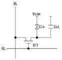
도 2는 도 1에 도시된 액정표시패널의 픽셀을 보여 주는 등가 도면이다.
도 3은 도 1에 도시된 소스 드라이브 IC를 상세히 보여 주는 도면이다.
도 4는 도 1에 도시된 게이트 드라이브 IC를 상세히 보여 주는 회로도이다.
도 5a 내지 도 5d는 도 1에 도시된 화면 영역 A, B, C, D를 구동하기 위한 소스 드라이브 IC와 게이트 드라이브 IC의 출력 타이밍을 제어하는 소스 출력 인에이블신호와 게이트 출력 인에이블신호를 보여 주는 파형도들이다.
도 6은 도 3에 도시된 차지쉐어회로를 상세히 보여 주는 도면이다.
도 7은 소스 출력 인에이블신호와 차지쉐어 동작 타이밍을 보여 주는 타이밍도이다.
도 8은 차지 쉐어링 시간 변화에 따른 소스 드라이브 IC의 온도 변화를 보여 주는 실험 결과 도면이다.
도 9a 내지 도 9d는 도 1에 도시된 화면 영역 A, B, C, D를 구동하기 위한 소스 드라이브 IC와 게이트 드라이브 IC의 출력 타이밍을 제어하는 본 발명의 소스 출력 인에이블신호와 게이트 출력 인에이블신호를 보여 주는 파형도들이다.
도 10은 본 발명의 타이밍 콘트롤러에 의해 변조된 소스 출력 인에이블신호와 게이트 출력 인에이블신호를 보여 주는 파형도이다.
도 11은 본 발명의 다른 실시예에 따른 액정표시장치를 보여 주는 도면이다.
도 12는 도 11에 도시된 레벨 시프터를 상세히 보여 주는 회로도이다.1 is a view illustrating a liquid crystal display device according to an embodiment of the present invention.
FIG. 2 is an equivalent diagram illustrating pixels of the liquid crystal display panel illustrated in FIG. 1.
3 is a view showing in detail the source drive IC shown in FIG.
4 is a circuit diagram showing in detail the gate drive IC shown in FIG.
5A to 5D show a source output enable signal and a gate output enable signal for controlling output timings of a source drive IC and a gate drive IC for driving the screen regions A, B, C, and D shown in FIG. The waveforms are given.
6 is a view showing in detail the charge share circuit shown in FIG.
7 is a timing diagram illustrating a source output enable signal and a charge share operation timing.
8 is an experimental result diagram illustrating a temperature change of a source drive IC according to a change in charge sharing time.
9A to 9D illustrate a source output enable signal and a gate output enable of the present invention for controlling output timings of a source drive IC and a gate drive IC for driving the screen regions A, B, C, and D shown in FIG. These are waveform diagrams showing the signal.
FIG. 10 is a waveform diagram illustrating a source output enable signal and a gate output enable signal modulated by the timing controller of the present invention.
11 is a view showing a liquid crystal display according to another embodiment of the present invention.
FIG. 12 is a circuit diagram illustrating in detail the level shifter illustrated in FIG. 11.
이하 첨부된 도면을 참조하여 본 발명에 따른 바람직한 실시예들을 상세히 설명한다. 명세서 전체에 걸쳐서 동일한 참조번호들은 실질적으로 동일한 구성요소들을 의미한다. 이하의 설명에서, 본 발명과 관련된 공지 기능 혹은 구성에 대한 구체적인 설명이 본 발명의 요지를 불필요하게 흐릴 수 있다고 판단되는 경우, 그 상세한 설명을 생략한다.DETAILED DESCRIPTION OF THE PREFERRED EMBODIMENTS Reference will now be made in detail to the preferred embodiments of the present invention, examples of which are illustrated in the accompanying drawings. Like reference numerals throughout the specification denote substantially identical components. In the following description, when it is determined that a detailed description of known functions or configurations related to the present invention may unnecessarily obscure the subject matter of the present invention, the detailed description thereof will be omitted.
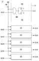
도 1 및 도 2를 참조하면, 본 발명의 실시예에 따른 액정표시장치는 화소 어레이가 형성된 액정표시패널(10), 액정표시패널(10)의 데이터라인들(DL)에 데이터전압을 공급하기 위한 데이터 구동회로, 액정표시패널(10)의 게이트라인들(GL)에 게이트펄스(또는 스캔펄스)를 순차적으로 공급하기 위한 게이트 구동회로, 및 데이터 구동회로와 게이트 구동회로의 동작 타이밍을 제어하기 위한 타이밍 콘트롤러(TCON) 등을 포함한다. 액정표시패널(10)의 아래에는 액정표시패널에 빛을 균일하게 조사하기 위한 백라이트 유닛이 배치될 수 있다.1 and 2, the liquid crystal display according to the exemplary embodiment of the present invention supplies a data voltage to the liquid
액정표시패널(10)은 액정층을 사이에 두고 대향하는 TFT(Thin Film Transistor) 어레이 기판과, 컬러필터(Color filter) 어레이 기판을 포함한다. TFT 어레이 기판은 데이터라인들(DL), 데이터라인들(DL)과 교차되는 게이트라인들(GL), 데이터라인들(DL)과 게이트라인들(GL)에 의해 정의된 화소 영역들에 형성된 픽셀들을 포함한다. 픽셀들 각각은 R, G, B 서브픽셀들을 포함할 수 있고, 서브픽셀들 각각은 데이터라인들(DL)과 게이트라인들(GL)의 교차부에 형성된 TFT들, 및 TFT에 접속된 액정셀(Clc), 액정셀(Clc)의 화소전극에 접속된 스토리지 커패시터(Storage Capacitor, Cst) 등을 포함한다. 컬러필터 어레이 기판에는 블랙매트릭스, 컬러필터 및 공통전극이 형성된다. 모든 픽셀들에 형성된 공통전극은 서로 전기적으로 연결되고, 공통전극에는 공통전압(Vcom)이 인가된다. 공통전극은 TN(Twisted Nematic) 모드와 VA(Vertical Alignment) 모드와 같은 수직전계 구동방식의 경우에 상부 유리기판 상에 형성되며, IPS(In-Plane Switching) 모드와 FFS(Fringe Field Switching) 모드와 같은 수평전계 구동방식의 경우에 화소전극과 함께 하부 유리기판 상에 형성된다. TFT 어레이 기판과 컬러필터 어레이 기판 각각에는 편광판이 부착되고 액정의 프리틸트각(pre-tilt angle)을 설정하기 위한 배향막이 형성된다.The liquid
액정표시패널(10)은 TN 모드, VA 모드, IPS 모드, FFS 모드뿐 아니라 어떠한 액정모드로도 구현될 수 있다. 본 발명의 액정표시장치는 투과형 액정표시장치, 반투과형 액정표시장치, 반사형 액정표시장치 등 어떠한 형태로도 구현될 수 있다. 투과형 액정표장치와 반투과형 액정표시장치에서는 백라이트 유닛이 필요하다. 백라이트 유닛은 직하형(direct type) 백라이트 유닛 또는, 에지형(edge type) 백라이트 유닛으로 구현될 수 있다.The liquid
데이터 구동회로는 다수의 소스 드라이브 IC들(SDIC1~SDIC4)을 포함한다. 게이트 구동회로는 다수의 게이트 드라이브 IC들(GDIC1~GDIC4)을 포함한다.The data driving circuit includes a plurality of source drive ICs SDIC1 to SDIC4. The gate driving circuit includes a plurality of gate drive ICs GDIC1 to GDIC4.
타이밍 콘트롤러(TCON)은 콘트롤 PCB(CPCB) 상에 실장된다. 타이밍 콘트롤러(TCON)는 LVDS(Low Voltage Differential Signaling) 인터페이스, TMDS(Transition Minimized Differential Signaling) 인터페이스 등의 인터페이스를 통해 외부의 호스트 시스템으로부터 디지털 비디오 데이터(RGB)를 입력 받는다. 타이밍 콘트롤러(TCON)는 호스트 컴퓨터로부터 입력 받은 디지털 비디오 데이터들(RGB)을 소스 드라이브 IC들(SDIC1~SDIC4)로 전송한다. 콘트롤 PCB(PCB)에는 도시하지 않은 직류-직류 변환기(DC-DC Convertor)가 실장될 수 있다. 직류-직류 변환기는 액정표시패널(10)에 공급되는 아날로그 구동 전원들을 발생한다. 구동 전원들은 정극성/부극성 감마기준전압, 공통전압(Vcom), 게이트 하이전압(VGH), 게이트 로우전압(VGL) 등을 포함한다. 콘트롤 PCB(CPCB)는 FFC(Flexible Flat Cable)를 통해 소스 PCB(SPCB)에 전기적으로 연결된다.The timing controller TCON is mounted on the control PCB CPCB. The timing controller TCON receives digital video data (RGB) from an external host system through an interface such as a low voltage differential signaling (LVDS) interface and a transition minimized differential signaling (TMDS) interface. The timing controller TCON transmits the digital video data RGB received from the host computer to the source drive ICs SDIC1 to SDIC4. A DC-DC converter (not shown) may be mounted on the control PCB. The DC-DC converter generates analog driving power supplies supplied to the liquid
타이밍 콘트롤러(TCON)는 LVDS 또는 TMDS 인터페이스 수신회로를 통해 호스트 시스템으로부터 수직 동기신호(Vsync), 수평 동기신호(Hsync), 데이터 인에이블 신호(Data Enable, DE), 메인 클럭(MCLK) 등의 타이밍신호를 입력받는다. 타이밍 콘트롤러(TCON)는 호스트 시스템으로부터의 타이밍 신호를 기준으로 소스 드라이브 IC들(SDIC1~SDIC4)과 게이트 드라이브 IC들(GDIC1~GDIC4)의 동작 타이밍을 제어하기 위한 타이밍 제어신호들을 발생한다. 타이밍 제어신호들은 게이트 드라이브 IC들(GDIC1~GDIC4)의 동작 타이밍을 제어하기 위한 게이트 타이밍 제어신호들과, 소스 드라이브 IC들(SDIC1~SDIC4)의 동작 타이밍과 데이터전압의 극성을 제어하기 위한 데이터 타이밍 제어신호들을 포함한다.The timing controller TCON uses the LVDS or TMDS interface receiving circuit to control the timing of the vertical synchronization signal Vsync, the horizontal synchronization signal Hsync, the data enable signal Data Enable, DE, and the main clock MCLK. Receive a signal. The timing controller TCON generates timing control signals for controlling operation timings of the source drive ICs SDIC1 to SDIC4 and the gate drive ICs GDIC1 to GDIC4 based on the timing signal from the host system. The timing control signals include gate timing control signals for controlling the operation timing of the gate drive ICs GDIC1 to GDIC4, data timing for controlling the operation timing and polarity of the data voltages of the source drive ICs SDIC1 to SDIC4. Control signals.
게이트 타이밍 제어신호들은 게이트 스타트 펄스(GSP), 게이트 시프트 클럭(GCLK1~n), 플리커 제어신호(FLK), 게이트 출력 인에이블신호(GOE) 등을 포함한다. 게이트 스타트 펄스(Gate Start Pulse, GSP)는 제1 게이트 드라이브 IC(GDIC1)에 입력되어 제1 게이트 드라이브 IC(GDIC1)로부터 첫 번째 출력되는 제1 게이트펄스의 출력 타이밍을 제어한다. 게이트 시프트 클럭(Gate Shift Clock, GSC)은 게이트 스타트 펄스(GSP)의 시프트 타이밍을 제어한다. 플리커 제어신호(FLK)는 게이트펄스의 폴링에지에서 게이트 하이전압(VGH)을 낮게 변조하여 플리커를 줄이기 위한 변조 타이밍을 제어한다. 게이트 출력 인에이블신호(GOE)는 게이트 드라이브 IC들(GDIC1~GDIC4)의 출력 타이밍을 제어한다. 게이트 타이밍 제어신호들은 콘트롤 PCB(CPCB)에 형성된 게이트 타이밍 제어신호 버스라인들, FFC, 소스 PCB(SPCB)에 형성된 게이트 타이밍 제어신호 버스라인들, 소스 드라이브 IC들(SDIC1) 중에서 하나 이상의 TCP에 형성된 게이트 타이밍 제어신호 버스라인, 및 액정표시패널(10)의 TFT 어레이 기판에 형성된 LOG(Line On Glass) 라인들을 통해 게이트 드라이브 IC들(GDIC1~GDIC4)에 전송된다.The gate timing control signals include a gate start pulse GSP, gate shift clocks GCLK1 to n, a flicker control signal FLK, a gate output enable signal GOE, and the like. The gate start pulse GSP is input to the first gate drive IC GDIC1 to control the output timing of the first gate pulse first output from the first gate drive IC GDIC1. The gate shift clock GSC controls the shift timing of the gate start pulse GSP. The flicker control signal FLK controls the modulation timing for reducing flicker by modulating the gate high voltage VGH low at the falling edge of the gate pulse. The gate output enable signal GOE controls the output timing of the gate drive ICs GDIC1 to GDIC4. The gate timing control signals are formed on one or more TCPs among the gate timing control signal bus lines formed on the control PCB (CPCB), the FFC, the gate timing control signal bus lines formed on the source PCB (SPCB), and the source drive ICs SDIC1. The gate timing control signal bus lines and the LOG (Line On Glass) lines formed on the TFT array substrate of the liquid
데이터 타이밍 제어신호들은 소스 스타트 펄스(Source Start Pulse, SSP), 소스 샘플링 클럭(Source Sampling Clock, SSC), 극성제어신호(Polarity, POL), 및 소스 출력 인에이블신호(Source Output Enable, SOE) 등을 포함한다. 소스 스타트 펄스(SSP)는 소스 드라이브 IC들(SDIC1~SDIC4)의 시프트 스타트 타이밍을 제어한다. 소스 샘플링 클럭(SSC)은 소스 드라이브 IC들(SDIC1~SDIC4) 내에서 데이터의 샘플링 타이밍을 제어한다. 극성제어신호(POL)는 소스 드라이브 IC들(SDIC1~SDIC4)로부터 출력되는 데이터전압의 극성을 제어한다. 소스 출력 인에이블신호(SOE)는 소스 드라이브 IC들(SDIC1~SDIC4)의 데이터전압 출력 타이밍과 차지 쉐어링 타이밍(Charge sharing timing)을 제어한다. 타이밍 콘트롤러(TCON)와 소스 드라이브 IC들(SDIC1~SDIC4) 사이의 데이터 전송 인터페이스가 mini LVDS 인터페이스라면, 소스 스타트 펄스(SSP)와 소스 샘플링 클럭(SSC)은 생략될 수 있다. 데이터 타이밍 제어신호들은 콘트롤 PCB(CPCB)에 형성된 데이터 타이밍 제어신호 버스라인들, FFC, 및 소스 PCB(SPCB)에 형성된 데이터 타이밍 제어신호 버스라인들을 통해 소스 드라이브 IC들(SDIC1)에 전송된다.The data timing control signals include a source start pulse (SSP), a source sampling clock (SSC), a polarity control signal (Polarity, POL), and a source output enable signal (Source Output Enable, SOE). It includes. The source start pulse SSP controls the shift start timing of the source drive ICs SDIC1 to SDIC4. The source sampling clock SSC controls sampling timing of data in the source drive ICs SDIC1 to SDIC4. The polarity control signal POL controls the polarity of the data voltages output from the source drive ICs SDIC1 to SDIC4. The source output enable signal SOE controls the data voltage output timing and the charge sharing timing of the source drive ICs SDIC1 to SDIC4. If the data transfer interface between the timing controller TCON and the source drive ICs SDIC1 to SDIC4 is a mini LVDS interface, the source start pulse SSP and the source sampling clock SSC may be omitted. The data timing control signals are transmitted to the source drive ICs SDIC1 through the data timing control signal buslines formed on the control PCB CPCB, the FFC, and the data timing control signal buslines formed on the source PCB SPCB.
소스 드라이브 IC들(SDIC1~SDIC4) 각각은 타이밍 콘트롤러(TCON)로부터 디지털 비디오 데이터를 입력받는다. 소스 드라이브 IC들(SDIC1~SDIC4)은 타이밍 콘트롤러(TCON)로부터의 소스 타이밍 제어신호에 응답하여 디지털 비디오 데이터를 정극성/부극성 아날로그 데이터전압으로 변환하여 액정표시패널(10)의 데이터라인들(DL)에 공급한다. 소스 드라이브 IC들(SDIC1~SDIC4) 각각은 COG(Chip On Glass) 공정에 의해 액정표시패널(10)의 TFT 어레이 기판 상에 접착될 수 있다. 소스 드라이브 IC들(SDIC1~SDIC4)은 TCP(Tape Carrier Package) 상에 실장되어 TAB(Tape Automated Bonding) 공정으로 소스 PCB(Printed Circuit Board, SPCB)와 액정표시패널(10)의 TFT 어레이 기판에 접착될 수 있다.Each of the source drive ICs SDIC1 to SDIC4 receives digital video data from the timing controller TCON. The source drive ICs SDIC1 to SDIC4 convert the digital video data into positive / negative analog data voltages in response to the source timing control signal from the timing controller TCON, thereby providing data lines of the liquid
게이트 드라이브 IC들(GDIC1~GDIC4)은 타이밍 콘트롤러(TCON)로부터의 게이트 타이밍 제어신호에 응답하여 액정표시패널(10)의 게이트라인들(GL)에 게이트펄스를 순차적으로 공급한다. 게이트펄스는 게이트 하이전압(VGH)과 게이트 로우전압(VGL) 사이에서 스윙한다. 게이트 하이전압(VGH)은 액정표시패널(10)의 TFT 어레이에 형성된 TFT들의 문턱전압 이상의 전압으로 설정되며, 게이트 로우전압(VGL)은 액정표시패널(10)의 TFT 어레이에 형성된 TFT들의 문턱전압보다 낮은 전압으로 설정된다. 따라서, TFT 어레이의 TFT들은 게이트라인(GL)으로부터의 게이트펄스에 응답하여 턴-온되어 데이터라인(DL)으로부터의 데이터전압을 액정셀(Clc)의 화소전극에 공급한다. 게이트 드라이브 IC들(GDIC1~GDIC4)은 TCP 상에 실장되어 TAB 공정에 의해 액정표시패널(10)의 TFT 어레이 기판 상에 접착될 수 있다. 게이트 구동회로는 도 1과 같이 액정표시패널(10)의 양측 가장자리에 접착되어 게이트라인들(GL)의 양 끝단에 게이트펄스를 동시에 인가하여 게이트펄스의 지연을 줄일 수 있다. 또한, 게이트 구동회로는 액정표시패널(10)의 일측 가장자리에 접착되어 액정표시패널(10)의 일측 가장자리에 게이트펄스를 인가할 수도 있다. 한편, 게이트 구동회로는 도 11 및 도 12와 같이 GIP(Gate In Panel) 공정에 의해 TFT 어레이와 함께 TFT 어레이 기판에 직접 형성되는 GIP 회로로 구현될 수 있다.The gate drive ICs GDIC1 to GDIC4 sequentially supply gate pulses to the gate lines GL of the liquid
도 3은 소스 드라이브 IC들(SDIC1~SDIC4)의 회로 구성을 보여 주는 도면이다.3 is a diagram illustrating a circuit configuration of the source drive ICs SDIC1 to SDIC4.
도 3을 참조하면, 소스 드라이브 IC들(SDIC1~SDIC4) 각각은 m(m은 자연수) 보다 작은 양의 정수) 개의 데이터라인들(D1~Dm)을 구동하며, 데이터 복원부(21),시프트 레지스터(22), 제1 래치 어레이(23), 제2 래치 어레이(24), 디지털-아날로그 변환기(이하, "DAC"라 한다)(25), 출력 버퍼(26), 차지쉐어회로(Charge Share Circuit)(27) 등을 포함한다.Referring to FIG. 3, each of the source drive ICs SDIC1 to SDIC4 drives m (m is a positive integer less than a natural number) data lines D1 to Dm, and the
데이터 복원부(21)는 mini LVDS 인터페이스 전송 체계로 입력된 디지털 비디오 데이터(RGBWodd, RGBeven)를 복원하여 제1 래치 어레이(23)에 공급한다. 시프트 레지스터(22)는 소스 샘플링 클럭(SSC)에 따라 샘플링신호를 시프트시킨다. 시프트 레지스터(22)는 제1 래치 어레이(23)의 래치수를 초과하는 데이터가 공급될 때 캐리신호(Carry signal, CAR)를 발생한다.The
제1 래치 어레이(23)는 시프트 레지스터(22)로부터 순차적으로 입력되는 샘플링신호에 응답하여 데이터 복원부(21)로부터 직렬로 입력되는 디지털 비디오 데이터(RGBWodd, RGBWeven)를 샘플링하고 래치한 다음, 동시에 출력함으로써 직렬 체계의 데이터를 병렬 체계의 데이터로 변환한다. 제2 래치 어레이(24)는 제1 래치 어레이(23)로부터 입력되는 데이터들을 래치한 다음, 다른 소스 드라이브 IC들의 제2 래치 어레이(24)와 동시에 래치된 데이터들을 출력한다.The
DAC(25)는 정극성 감마기준전압들(PGMA)과 부극성 감마기준전압들(NGMA)을 이용하여 제2 래치 어레이(24)로부터 입력되는 디지털 비디오 데이터를 정극성 데이터전압과 부극성 데이터전압으로 변환한다. 그리고 DAC(25)는 극성제어신호(POL)의 논리값에 따라 정극성 데이터전압과 부극성 데이터전압을 교대로 선택하여 출력한다.The DAC 25 converts digital video data input from the
출력 버퍼(26)는 데이터라인들(D1~Dm)에 공급되는 데이터전압의 신호감쇠를 최소화한다. 차지쉐어회로(27)는 소스 출력 인에이블신호(SOE)의 로우 로직(Low logic) 기간 동안 정극성/부극성 데이터전압을 데이터라인들(D1~Dm)에 공급하는 반면, 소스 출력 인에이블신호(SOEO)의 하이 로직(High logic) 기간 동안 이웃한 데이터 출력채널들을 단락(short)시켜 데이터라인들(D1~Dm)의 전압을 정극성 데이터전압과 부극성 데이터 전압의 평균 전압으로 평균화한다.The
소스 드라이브 IC들(SDIC1~SDIC4)의 배치와 동작 관계를 살펴 보면, 제1 소스 드라이브 IC(SDIC1)는 화면의 좌측에 배치되고 제2 내지 제4 소스 드라이브 IC들(SDIC2~SDIC4)은 그 순번 대로 제1 소스 드라이브 IC(SDIC1)의 우측에 배치된다. 제1 소스 드라이브 IC(SDIC1)는 화면의 A 및 C 부분을 포함한 좌측 부분에 배치된 데이터라인들에 데이터전압을 공급하고, 제4 소스 드라이브 IC(SDIC4)는 화면의 B 및 D를 포함한 중앙(또는 우측) 부분에 배치된 데이터라인들에 데이터전압을 공급한다. 제2 내지 제3 소스 드라이브 IC들(SDIC2, SDIC3)은 화면에서 A/C 부분과 B/D 부분 사이에 배치된 데이터라인들에 데이터전압을 공급한다.Looking at the arrangement and the operation relationship of the source drive ICs SDIC1 to SDIC4, the first source drive IC SDIC1 is disposed on the left side of the screen, and the second to fourth source drive ICs SDIC2 to SDIC4 are sequentially numbered. As shown, the right side of the first source drive IC SDIC1 is disposed. The first source drive IC SDIC1 supplies data voltages to the data lines arranged on the left side including the A and C portions of the screen, and the fourth source drive IC SDIC4 includes the center (including B and D of the screen). Alternatively, the data voltage is supplied to the data lines arranged at the right side). The second to third source drive ICs SDIC2 and SDIC3 supply data voltages to data lines disposed between the A / C portion and the B / D portion on the screen.
제1 소스 드라이브 IC(SDIC1)는 소스 스타트 펄스(SSP) 또는 mini LVDS 클럭의 리셋클럭에 응답하여 자신의 데이터 출력 채널만큼 직렬 데이터를 순차적으로 샘플링한 후에 제1 캐리신호(CAR)를 제2 소스 드라이브 IC(SDIC2)에 전달한다. 제2 소스 드라이브 IC(SDIC2)는 제1 소스 드라이브 IC(SDIC1)로부터의 제1 캐리신호(CAR)에 응답하여 자신의 데이터 출력 채널만큼 데이터를 샘플링한 후에 제2 캐리신호(CAR)를 제3 소스 드라이브 IC(SDIC3)에 전달한다. 제3 소스 드라이브 IC(SDIC3)는 제2 소스 드라이브 IC(SDIC2)로부터의 제2 캐리신호(CAR)에 응답하여 자신의 데이터 출력 채널만큼 데이터를 샘플링한 후에 제3 캐리신호(CAR)를 제4 소스 드라이브 IC(SDIC4)에 전달한다. 제4 소스 드라이브 IC(SDIC4)는 제3 소스 드라이브 IC(SDIC3)로부터의 제3 캐리신호(CAR)에 응답하여 자신의 데이터 출력 채널만큼 데이터를 샘플링한다. 이렇게 소스 드라이브 IC들(SDIC1~SDIC4)은 직렬로 입력되는 데이터를 순차적으로 샘플링하고 래치하여 직렬 체계의 데이터를 병렬 체계의 데이터로 변환한 다음, 소스 출력 인에이블신호(SOE)에 응답하여 동시에 출력한다.The first source drive IC SDIC1 sequentially samples the serial data by its data output channel in response to the source start pulse SSP or the reset clock of the mini LVDS clock, and then supplies the first carry signal CAR to the second source. Transfer to drive IC (SDIC2). The second source drive IC SDIC2 samples the second carry signal CAR after the data has been sampled by its own data output channel in response to the first carry signal CAR from the first source drive IC SDIC1. To the source drive IC (SDIC3). The third source drive IC SDIC3 samples the data by the data output channel of the third source signal IC in response to the second carry signal CAR from the second source drive IC SDIC2, and then applies the third carry signal CAR to the fourth. Transfer to the source drive IC (SDIC4). The fourth source drive IC SDIC4 samples data by its data output channel in response to the third carry signal CAR from the third source drive IC SDIC3. In this way, the source drive ICs SDIC1 to SDIC4 sequentially sample and latch data input serially, convert the data of the serial system into data of the parallel system, and simultaneously output the data in response to the source output enable signal SOE. do.
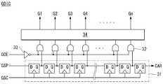
도 4는 게이트 드라이브 IC들(GDIC1~GDIC4)의 회로 구성을 보여 주는 도면이다.4 is a diagram illustrating a circuit configuration of the gate drive ICs GDIC1 to GDIC4.
도 4를 참조하면, 게이트 드라이브 IC 각각은 시프트 레지스터(31), 레벨 쉬프터(34), 시프트 레지스터(31)와 레벨 쉬프터(34) 사이에 접속된 다수의 AND 게이트(32) 등을 포함한다.Referring to FIG. 4, each of the gate drive ICs includes a
시프트 레지스터(31)는 종속적으로 접속된 다수의 D-플립플롭을 이용하여 게이트 스타트 펄스(GSP)를 게이트 시프트 클럭(GSC)에 따라 순차적으로 시프트킨 후에 캐리신호(CAR)를 발생한다. AND 게이트들(32) 각각은 시프트 레지스터(31)의 출력신호와, 인버터(33)에 의해 반전된 게이트 출력 인에이블신호(GOE)의 논리곱 연산 결과를 출력한다.The
레벨 쉬프터(34)는 AND 게이트(32)의 출력전압 스윙폭을 게이트 하이전압(VGH)과 게이트 로우전압(VGL) 사이의 스윙폭으로 변환하여 게이트라인들(G1~Gn)에 순차적으로 공급한다. 한편, 레벨 쉬프터(34)는 GIP 회로에서 시프트 레지스터(31)의 앞단에 배치된다.The
게이트 드라이브 IC들(GDIC1~GDIC4)의 배치와 동작 관계를 살펴 보면, 제1 게이트 드라이브 IC(GDIC1)는 화면의 상단에 배치되고 제2 내지 제4 게이트 드라이브 IC들(GDIC2~GDIC4)은 그 순번대로 제1 게이트 드라이브 IC(GDIC1)의 아래에 배치된다. 제1 게이트 드라이브 IC(GDIC1)는 화면의 A 및 B 부분을 포함한 상단 부분에 배치된 게이트라인들에 게이트펄스를 순차적으로 공급하고, 제4 소스 드라이브 IC(SDIC4)는 화면의 C 및 D를 포함한 하단 부분에 배치된 게이트라인들에 게이트펄스를 순차적으로 공급한다. 제2 내지 제3 게이트 드라이브 IC들(GDIC2, GDIC3)은 화면에서 A/B 부분과 C/D 부분 사이에 배치된 게이트라인들에 게이트펄스를 순차적으로 공급한다.Looking at the arrangement and operation relationship of the gate drive ICs GDIC1 to GDIC4, the first gate drive IC GDIC1 is disposed at the top of the screen, and the second to fourth gate drive ICs GDIC2 to GDIC4 are in turn. As such, it is disposed under the first gate drive IC GDIC1. The first gate drive IC GDIC1 sequentially supplies gate pulses to gate lines disposed in the upper part including the A and B portions of the screen, and the fourth source drive IC SDIC4 includes the C and D of the screen. Gate pulses are sequentially supplied to the gate lines arranged at the lower portion. The second to third gate drive ICs GDIC2 and GDIC3 sequentially supply gate pulses to gate lines disposed between the A / B portion and the C / D portion on the screen.
제1 게이트 드라이브 IC(GDIC1)는 게이트 쉬프트 클럭(GSC)의 라이징 에지에 동기하여 게이트 스타트 펄스(SSP)를 시프트시킴으로써 게이트라인들에 게이트펄스를 순차 출력한 후에, 제1 캐리신호(CAR)를 제2 게이트 드라이브 IC(GDIC2)의 스타트 펄스로서 출력한다. 제2 게이트 드라이브 IC(GDIC2)는 게이트 쉬프트 클럭(GSC)의 라이징 에지에 동기하여 제1 캐리신호(CAR)를 시프트시킴으로써 게이트라인들에 게이트펄스를 순차 출력한 후에, 제2 캐리신호(CAR)를 제3 게이트 드라이브 IC(GDIC3)의 스타트 펄스로서 출력한다. 제3 게이트 드라이브 IC(GDIC3)는 게이트 쉬프트 클럭(GSC)의 라이징 에지에 동기하여 제2 캐리신호(CAR)를 시프트시킴으로써 게이트라인들에 게이트펄스를 순차 출력한 후에, 제3 캐리신호(CAR)를 제4 게이트 드라이브 IC(GDIC4)의 스타트 펄스로서 출력한다. 제4 게이트 드라이브 IC(GDIC4)는 게이트 쉬프트 클럭(GSC)의 라이징 에지에 동기하여 제3 캐리신호(CAR)를 시프트시킴으로써 게이트라인들에 게이트펄스를 순차 출력한다.The first gate drive IC GDIC1 sequentially outputs the gate pulses to the gate lines by shifting the gate start pulse SSP in synchronization with the rising edge of the gate shift clock GSC, and then outputs the first carry signal CAR. It outputs as a start pulse of 2nd gate drive IC (GDIC2). The second gate drive IC GDIC2 sequentially outputs the gate pulses to the gate lines by shifting the first carry signal CAR in synchronization with the rising edge of the gate shift clock GSC, and then the second carry signal CAR. Is output as a start pulse of the third gate drive IC (GDIC3). After the third gate drive IC GDIC3 sequentially outputs the gate pulses to the gate lines by shifting the second carry signal CAR in synchronization with the rising edge of the gate shift clock GSC, the third carry signal CAR is applied. Is output as the start pulse of the fourth gate drive IC (GDIC4). The fourth gate drive IC GDIC4 sequentially outputs gate pulses to the gate lines by shifting the third carry signal CAR in synchronization with the rising edge of the gate shift clock GSC.
도 5a 내지 도 5d는 소스 출력 인에이블신호(SOE)와 게이트 출력 인에이블신호(GOE), 소스 드라이브 IC들(SDIC1~SDIC4)의 출력, 및 게이트 드라이브 IC들(GDIC1~GDIC4)의 출력을 화면 위치에 따라 구분하여 보여 주는 파형도들이다.5A to 5D illustrate a source output enable signal SOE and a gate output enable signal GOE, outputs of the source drive ICs SDIC1 to SDIC4, and outputs of the gate drive ICs GDIC1 to GDIC4. The waveform diagrams are shown according to their location.
도 5a 내지 도 5d를 참조하면, TA는 A 영역에 존재하는 액정셀(Clc)의 데이터 충전시간, TB는 B 영역에 존재하는 액정셀(Clc)의 데이터 충전시간, TC는 C 영역에 존재하는 액정셀(Clc)의 데이터 충전시간, 그리고 TD는 D 영역에 존재하는 액정셀(Clc)의 데이터 충전시간을 각각 나타낸다.5A to 5D, TA is a data charging time of the liquid crystal cell Clc in the A region, TB is a data charging time of the liquid crystal cell Clc in the B region, and TC is present in the C region. The data charging time of the liquid crystal cell Clc and TD represent the data charging time of the liquid crystal cell Clc existing in the D region.
소스 드라이브 IC들(SDIC1~SDIC4)로부터 출력된 데이터전압과 게이트 드라이브 IC들(GDIC1~GDIC4)로부터 출력된 게이트펄스는 데이터라인들과 게이트라인들의 라인 저항과 액정표시패널(10)의 정전용량(capacitance) 값에 따른 RC 딜레이로 인하여 지연된다. 따라서, 액정표시패널(10)의 픽셀 위치에 따라 데이터전압과 게이트펄스의 지연시간이 다르므로 픽셀 위치에 따라 액정셀(Clc)의 데이터 충전양이 상이하다. 예를 들어, 도 1의 화면 영역 A, B, C 및 D 중에서 액정셀(Clc)의 데이터 충전 특성이 가장 나쁜(worst) 영역은 소스 드라이브 IC의 출력의 지연시간이 크고 게이트 드라이브 IC의 지연시간이 작은 C 영역(도 5c 참조)이다. 반면에, 액정셀(Clc)의 데이터 충전 특성이 가장 좋은(Best) 영역은 소스 드라이브 IC의 출력 지연시간이 작고 게이트 드라이브 IC의 지연시간이 큰 B 영역(도 5b 참조)이다. A 및 D 영역에 존재하는 액정셀(Clc)의 충전 특성은 C 영역에 존재하는 액정셀(Clc)의 충전 특성보다 좋고 B 영역에 존재하는 액정셀의 충전 특성 보다 나쁘다.The data voltages output from the source drive ICs SDIC1 to SDIC4 and the gate pulses output from the gate drive ICs GDIC1 to GDIC4 correspond to the line resistances of the data lines and gate lines and the capacitance of the liquid
소스 드라이브 IC들(SDIC1~SDIC4)의 동작 타이밍과 게이트 드라이브 IC들(GDIC1~GDIC4)의 동작 타이밍을 액정표시패널(10)에서 충전 특성이 가장 나쁜 위치를 기준으로 튜닝될 수 있다. 예를 들어, 액정셀(Clc)의 데이터 충전 특성이 가장 나쁜 C 영역을 고려하여 소스 출력 인에이블신호(SOE)와 게이트 출력 인에이블신호(GOE)의 최적 타이밍을 결정하여 화면의 모든 영역들에 적용하면, C 영역을 제외한 다른 영역들(A, B, D)을 구동하는 소스 드라이브 IC들(SDIC1~SDIC4)의 파워 소모와 온도를 최적화할 수 없다. 소스 드라이브 IC들(SDIC1~SDIC4)의 파워 소모와 온도는 차지 쉐어링 타이밍을 길게 하면 개선될 수 있다.The operation timings of the source drive ICs SDIC1 to SDIC4 and the operation timings of the gate drive ICs GDIC1 to GDIC4 may be tuned based on a position where the charging characteristic is worst in the liquid
도 6은 도 3에 도시된 차지쉐어회로(27)를 상세히 보여 주는 도면이다. 도 7은 소스 출력 인에이블신호와 차지쉐어 동작 타이밍을 보여 주는 타이밍도이다.6 is a view showing in detail the
도 6 및 도 7을 참조하면, 소스 드라이브 IC들(SDIC1~SDIC4)의 차지쉐어회로(27)는 출력 버퍼(BUF)와 데이터 출력 채널 사이에 직렬 접속된 제1 스위치들(SW1), 및 이웃하는 데이터 출력 채널들 사이에 접속된 제2 스위치들(SW2)을 포함한다. 소스 드라이브 IC들(SDIC1~SDIC4)의 데이터 출력 채널들은 액정표시패널(10)의 데이터라인들(D1~D3)과 1 : 1로 접속되어 출력 버퍼(BUF)로부터의 정극성/부극성 데이터전압을 데이터라인들(D1~D3)에 공급한다.6 and 7, the
제1 스위치들(SW1) 각각은 소스 출력 인에이블신호(SOE)의 로우 로직에 응답하여 턴-온(turn-on)되어 데이터전압을 데이터라인(D1~D3)에 공급한다. 반면에, 제1 스위치들(SW1)은 소스 출력 인에이블신호(SOE)의 하이 로직 구간에 턴-오프(turn-off)되어 출력 버퍼(BUF)와 데이터라인(D1~D3) 사이의 전류패스를 차단한다. 따라서, 소스 드라이브 IC들(SDIC1~SDIC4)은 소스 출력 인에이블신호(SOE)의 로우 로직 기간(또는 pulse off 구간) 동안 정극성/부극성 데이터전압을 출력하고 그 때 데이터전압의 스윙폭에 비례하는 전류가 발생되므로 파워가 소모된다.Each of the first switches SW1 is turned on in response to the low logic of the source output enable signal SOE to supply the data voltages to the data lines D1 to D3. On the other hand, the first switches SW1 are turned off during the high logic period of the source output enable signal SOE so that a current path between the output buffer BUF and the data lines D1 to D3 is provided. To block. Accordingly, the source drive ICs SDIC1 to SDIC4 output positive / negative data voltages during the low logic period (or pulse off period) of the source output enable signal SOE, and are proportional to the swing width of the data voltages. Power is consumed because a current is generated.
제2 스위치들(SW2) 각각은 소스 출력 인에이블신호(SOE)의 하이 로직에 응답하여 턴-온되어 이웃하는 데이터 출력 채널들을 접속시켜 데이터라인들(D1~D3)을 쇼트 회로(Short circuit)로 구성한다. 이웃하는 데이터라인들에는 서로 상반된 극성의 데이터전압이 공급된다. 그 결과, 소스 출력 인에이블신호(SOE)의 하이 로직 기간(또는 pulse on 구간 W1) 동안 데이터라인들은 정극성 데이터전압과 부극성 데이터전압의 차지쉐어링으로 인하여 정극성 데이터전압과 부극성 데이터전압의 평균전압으로 조정된다. 차지 쉐어링 기간 동안, 소스 드라이브 IC들(SDIC1~SDIC4)은 전류 가 거의 발생되지 않으므로 그 파워 소모가 작아진다. 반면에, 제2 스위치들(SW2)은 소스 출력 인에이블신호(SOE)의 로우 로직 구간에 턴-오프되어 이웃한 데이터 출력 채널들 사이의 전류패스를 차단한다.Each of the second switches SW2 is turned on in response to the high logic of the source output enable signal SOE to connect neighboring data output channels to short the data lines D1 to D3. It consists of. Neighboring data lines are supplied with data voltages of opposite polarities. As a result, during the high logic period (or pulse on period W1) of the source output enable signal SOE, the data lines are charged with the positive data voltage and the negative data voltage due to the charge sharing of the positive data voltage and the negative data voltage. The average voltage is adjusted. During the charge sharing period, the source drive ICs (SDIC1 to SDIC4) generate little current and thus have low power consumption. On the other hand, the second switches SW2 are turned off in the low logic period of the source output enable signal SOE to block current paths between neighboring data output channels.
도 6 및 도 7에서 알 수 있는 바와 같이, 소스 드라이브 IC들(SDIC1~SDIC4)의 파워 소모는 소스 출력 인에이블신호(SOE)에 따라 결정되는 차지 쉐어링 기간을 크게 하면 줄일 수 있다. 한편, 차지 쉐어링 기간을 길게 하면 액정셀의 데이터 충전시간이 그 만큼 작아지므로 차지 쉐어링 기간은 액정셀의 데이터 충전시간을 고려하여 최적화되어야 한다.As can be seen in FIGS. 6 and 7, the power consumption of the source drive ICs SDIC1 to SDIC4 can be reduced by increasing the charge sharing period determined according to the source output enable signal SOE. On the other hand, if the charge sharing period is extended, the data charging time of the liquid crystal cell is reduced by that much, so the charge sharing period should be optimized in consideration of the data charging time of the liquid crystal cell.
소스 드라이브 IC들(SDIC1~SDIC4)의 차지 쉐어링은 소스 드라이브 IC들(SDIC1~SDIC4)의 파워 소모 뿐만 소스 드라이브 IC들(SDIC1~SDIC4)의 온도에도 큰 영향을 끼친다. 차지 쉐어링 동작 기간 동안 소스 드라이브 IC들(SDIC1~SDIC4)의 전류 발생이 작아진다. 따라서, 차지 쉐어링 시간을 길게 하면 소스 드라이브 IC들(SDIC1~SDIC4)의 온도를 줄일 수 있다.Charge sharing of the source drive ICs SDIC1 to SDIC4 greatly affects the power consumption of the source drive ICs SDIC1 to SDIC4 as well as the temperature of the source drive ICs SDIC1 to SDIC4. Current generation of the source drive ICs SDIC1 to SDIC4 is reduced during the charge sharing operation. Therefore, lengthening the charge sharing time can reduce the temperature of the source drive ICs SDIC1 to SDIC4.
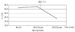
도 8은 차지 쉐어링 시간 변화에 따른 소스 드라이브 IC들(SDIC1~SDIC4)의 온도 변화를 보여 주는 실험 결과 도면이다. 도 8에서 알 수 있는 바와 같이, 소스 드라이브 IC들(SDIC1~SDIC4)이 차지 쉐어링 없이 구동되면 그 온도가 90℃ 이상으로 발열된다. 이에 비하여, 소스 드라이브 IC들(SDIC1~SDIC4)이 차지 쉐어링을 하면서 구동되면 그 온도가 90℃ 이하로 낮아진다. 차지 쉐어링 시간을 길게할 수록 즉, 소스 출력 인에이블신호(SOE)의 펄스폭을 길게 할수록 소스 드라이브 IC들(SDIC1~SDIC4)의 온도를 낮출 수 있다.FIG. 8 is an experimental result diagram illustrating a temperature change of the source drive ICs SDIC1 to SDIC4 according to the charge sharing time. As can be seen in FIG. 8, when the source drive ICs SDIC1 to SDIC4 are driven without charge sharing, their temperature is heated to 90 ° C. or more. On the other hand, when the source drive ICs SDIC1 to SDIC4 are driven with charge sharing, their temperature is lowered below 90 ° C. As the charge sharing time increases, that is, as the pulse width of the source output enable signal SOE is increased, the temperatures of the source drive ICs SDIC1 to SDIC4 may be lowered.
전술한 바와 같이, 소스 출력 인에이블신호(SOE)와 게이트 출력 인에이블신호(GOE)의 타이밍을 화면의 일부 영역을 기준으로 설정하고 그 타이밍을 화면 전체에 적용하면, 다른 화면 영역을 구동하는 소스 드라이브 IC들(SDIC1~SDIC4)의 파워 소모와 온도가 최적화되지 않는다. 본 발명의 타이밍 콘트롤러(TCON)는 모든 소스 드라이브 IC들(SDIC1~SDIC4)의 파워 소모와 온도를 최적화하기 위하여 소스 출력 인에이블신호(SOE)와 게이트 출력 인에이블신호(GOE)를 도 9a 내지 도 9d, 및 도 10과 같이 변조한다.As described above, when the timing of the source output enable signal SOE and the gate output enable signal GOE is set based on a part of the screen and the timing is applied to the entire screen, a source for driving another screen area is used. The power consumption and temperature of the drive ICs SDIC1 to SDIC4 are not optimized. The timing controller TCON of the present invention shows the source output enable signal SOE and the gate output enable signal GOE in order to optimize the power consumption and temperature of all the source drive ICs SDIC1 to SDIC4. 9d, and as shown in FIG.
도 9a 내지 도 9d는 도 1에 도시된 화면 영역 A, B, C, D를 구동하기 위한 소스 드라이브 IC(SDIC1~SDIC4)와 게이트 드라이브 IC(GDIC1~GDIC4)의 출력 타이밍을 제어하는 본 발명의 소스 출력 인에이블신호와 게이트 출력 인에이블신호를 보여 주는 파형도들이다. 도 10은 타이밍 콘트롤러(TCON)에 의해 변조된 소스 출력 인에이블신호와 게이트 출력 인에이블신호를 보여 주는 파형도이다.9A to 9D are diagrams illustrating embodiments of controlling output timings of the source drive ICs SDIC1 to SDIC4 and the gate drive ICs GDIC1 to GDIC4 for driving the screen areas A, B, C, and D shown in FIG. These waveform diagrams show the source output enable signal and the gate output enable signal. FIG. 10 is a waveform diagram illustrating a source output enable signal and a gate output enable signal modulated by the timing controller TCON.
도 9a 내지 도 9d, 및 도 10을 참조하면, 제1 소스 드라이브 IC(SDIC1)는 제1 소스 출력 인에이블신호(SOE for SDIC1)에 응답하여 화면의 A 및 C 영역에 배치된 데이터라인들로 데이터전압을 출력하고 그 데이터라인들을 차지 쉐어링한다. 제4 소스 드라이브 IC(SDIC4)는 제4 소스 출력 인에이블신호(SOE for SDIC4)에 응답하여 화면의 B 및 D 영역에 배치된 데이터라인들로 데이터전압을 출력하고 그 데이터라인들을 차지 쉐어링한다. 제2 및 제3 소스 드라이브 IC(SDIC2, SDIC3)는 제2 및 제3 소스 출력 인에이블신호(SOE for SDIC3, SOE for SDIC4)에 응답하여 화면의 A/C 및 B/D 영역 사이의 영역에 배치된 데이터라인들로 데이터전압을 출력하고 그 데이터라인들을 차지 쉐어링한다.9A through 9D and 10, the first source drive IC SDIC1 may be data lines disposed in areas A and C of the screen in response to the first source output enable signal SOE for SDIC1. Output a data voltage and charge share the data lines. In response to the fourth source output enable signal SOE for SDIC4, the fourth source drive IC SDIC4 outputs a data voltage to data lines disposed in areas B and D of the screen and charge-shares the data lines. The second and third source drive ICs SDIC2 and SDIC3 are configured to display an area between the A / C and B / D areas of the screen in response to the second and third source output enable signals SOE for SDIC3 and SOE for SDIC4. The data voltages are output to the arranged data lines and the charge sharing is performed on the data lines.
제1 게이트 드라이브 IC(GDIC1)는 게이트 출력 인에이블신호(GOE)에 응답하여 화면의 A 및 B 영역에 배치된 게이트라인들에 게이트펄스를 순차 출력한다. 제4 게이트 드라이브 IC(GDIC4)는 게이트 출력 인에이블신호(GOE)에 응답하여 화면의 C 및 D 영역에 배치된 게이트라인들에 게이트펄스를 순차 출력한다. 제2 및 제3 게이트 드라이브 IC(GDIC2, GDIC3)는 게이트 출력 인에이블신호(GOE)에 응답하여 화면의 A/B 및 C/D 영역 사이의 영역에 배치된 게이트라인들에 게이트펄스를 순차 출력한다.The first gate drive IC GDIC1 sequentially outputs gate pulses to gate lines disposed in areas A and B of the screen in response to the gate output enable signal GOE. The fourth gate drive IC GDIC4 sequentially outputs gate pulses to gate lines arranged in regions C and D of the screen in response to the gate output enable signal GOE. The second and third gate drive ICs GDIC2 and GDIC3 sequentially output gate pulses to gate lines disposed in an area between the A / B and C / D areas of the screen in response to the gate output enable signal GOE. do.
타이밍 콘트롤러(TCON)는 화면의 C 영역을 구동하기 위한 소스 출력 인에이블신호(SOE)와 게이트 출력 인에이블 신호를 기준으로 제1 내지 제4 소스 출력 인에이블신호들(SOE for SDIC1 ~ SOE for SDIC4)의 펄스폭 및 주기를 변조하고, 게이트 출력 인에이블신호(GOE)의 주기를 변조한다.The timing controller TCON uses the first to fourth source output enable signals SOE for SDIC1 to SOE for SDIC4 based on the source output enable signal SOE and the gate output enable signal for driving the C region of the screen. Modulates the pulse width and period, and modulates the gate output enable signal GOE.
제1 소스 출력 인에이블신호(SOE for SDIC1)의 펄스들(S11~S15)에서 라이징 에지 타이밍은 기존과 동일하다. 이에 비하여, 제1 소스 출력 인에이블신호(SOE for SDIC1)의 펄스들(S11~S14) 중 적어도 일부 펄스들의 폴링 에지 타이밍이 더 늦게 변조된다. 제1 소스 출력 인에이블신호(SOE for SDIC1)의 제1 펄스(S11)는 화면의 A 영역에 존재하는 데이터라인들에 공급되는 데이터전압의 출력 타이밍과 그 데이터라인들의 차지 쉐어링 타이밍을 정의한다. 제1 펄스(S11)의 폴링 에지 타이밍은 기존 보다 대략 3Δt만큼 더 지연될 수 있으며, 이 경우에 제1 펄스(S11)의 펄스폭은 기존 보다 3Δt만큼 더 넓어진다.(도 9a 및 도 10의 빗금친 부분)The rising edge timings of the pulses S11 to S15 of the first source output enable signal SOE for SDIC1 are the same as before. In contrast, the falling edge timing of at least some of the pulses S11 to S14 of the first source output enable signal SOE for SDIC1 is modulated later. The first pulse S11 of the first source output enable signal SOE for SDIC1 defines the output timing of the data voltage supplied to the data lines existing in the area A of the screen and the charge sharing timing of the data lines. The falling edge timing of the first pulse S11 may be delayed by approximately 3Δt more than before, and in this case, the pulse width of the first pulse S11 may be wider by 3Δt than before (see FIGS. 9A and 10). Hatched)
제1 소스 출력 인에이블신호(SOE for SDIC1)의 제2 펄스(S12)는 그 폴링 에지 타이밍이 기존보다 더 늦고 제1 펄스(S11)의 변조폭보다 작은 변조폭으로 변조된다. 예를 들어, 제2 펄스(S12)의 폴링 에지 타이밍은 기존 보다 대략 2Δt만큼 더 지연될 수 있으며, 이 경우에 제2 펄스(S12)의 펄스폭은 기존 보다 2Δt만큼 더 넓어진다.(도 9a 및 도 10 참조)The second pulse S12 of the first source output enable signal SOE for SDIC1 is modulated to a modulation width whose polling edge timing is later than the conventional one and smaller than the modulation width of the first pulse S11. For example, the falling edge timing of the second pulse S12 may be delayed by approximately 2Δt more than before, in which case the pulse width of the second pulse S12 becomes 2Δt wider than before (FIG. 9A). And FIG. 10)
제1 소스 출력 인에이블신호(SOE for SDIC1)의 제3 펄스(S13)는 그 폴링 에지 타이밍이 기존보다 더 늦고 제2 펄스(S12)의 변조폭보다 작은 변조폭으로 변조된다. 예를 들어, 제3 펄스(S13)의 폴링 에지 타이밍은 기존 보다 대략 Δt만큼 더 지연될 수 있으며, 이 경우에 제3 펄스(S13)의 펄스폭은 기존 보다 Δt만큼 더 넓어진다.(도 10 참조)The third pulse S13 of the first source output enable signal SOE for SDIC1 is modulated to a modulation width whose polling edge timing is later than the conventional one and smaller than the modulation width of the second pulse S12. For example, the falling edge timing of the third pulse S13 may be delayed by approximately Δt more than before, and in this case, the pulse width of the third pulse S13 may be wider by Δt than before (FIG. 10). Reference)
제1 소스 출력 인에이블신호(SOE for SDIC1)의 제4 펄스(S14)는 화면의 C 영역에 존재하는 데이터라인들에 공급되는 데이터전압의 출력 타이밍과 그 데이터라인들의 차지 쉐어링 타이밍을 정의한다. 제3 펄스(S13)의 폴링 에지는 제2 펄스(S12)의 변조폭보다 작은 변조폭으로 변조된다. 예를 들어, 제3 펄스(S13)의 폴링 에지 타이밍은 기존과 동일하게 설정될 수 있다. 이 경우에 제3 펄스(S13)의 펄스폭은 기존과 동일하다.(도 9c 및 도 10 참조)The fourth pulse S14 of the first source output enable signal SOE for SDIC1 defines the output timing of the data voltage supplied to the data lines existing in the C region of the screen and the charge sharing timing of the data lines. The falling edge of the third pulse S13 is modulated with a modulation width smaller than the modulation width of the second pulse S12. For example, the falling edge timing of the third pulse S13 may be set as it is. In this case, the pulse width of the third pulse S13 is the same as before (see Figs. 9C and 10).
제2 소스 출력 인에이블신호(SOE for SDIC2)의 펄스들(S21~S24) 중에서 적어도 일부는 라이징 에지 타이밍이 제1 소스 출력 인에이블신호(SOE for SDIC1) 보다 더 빠르게 변조된다. 제2 소스 출력 인에이블신호(SOE for SDIC2)의 펄스들(S21~S24)은 그 폴링 에지 타이밍이 제1 소스 출력 인에이블신호(SOE for SDIC1)과 동일하게 설정된다. 제2 소스 출력 인에이블신호(SOE for SDIC2)의 제1 펄스(S21)는 그 라이징 에지 타이밍이 제1 소스 출력 인에이블신호(SOE for SDIC1)의 제1 펄스(S11) 보다 대략 Δt만큼 더 빠르게 설정될 수 있다. 제2 소스 출력 인에이블신호(SOE for SDIC2)의 제1 펄스(S21)는 그 폴링 에지 타이밍이 제1 소스 출력 인에이블신호(SOE for SDIC1)의 제1 펄스(S11)와 동일하게 설정될 수 있다. 이 경우에 제1 펄스(S21)의 펄스폭은 제1 소스 출력 인에이블신호(SOE for SDIC1)의 제1 펄스(S11)보다 Δt만큼 더 넓어진다.(도 10 참조)At least some of the pulses S21 to S24 of the second source output enable signal SOE for SDIC2 are modulated with a rising edge timing faster than that of the first source output enable signal SOE for SDIC1. The pulses S21 to S24 of the second source output enable signal SOE for SDIC2 are set to have the same falling edge timing as the first source output enable signal SOE for SDIC1. The first pulse S21 of the second source output enable signal SOE for SDIC2 has a rising edge timing approximately Δt faster than the first pulse S11 of the first source output enable signal SOE for SDIC1. Can be set. The first pulse S21 of the second source output enable signal SOE for SDIC2 may be set to have the same falling edge timing as the first pulse S11 of the first source output enable signal SOE for SDIC1. have. In this case, the pulse width of the first pulse S21 is wider by Δt than the first pulse S11 of the first source output enable signal SOE for SDIC1 (see FIG. 10).
제2 소스 출력 인에이블신호(SOE for SDIC2)의 제2 펄스(S22)는 그 라이징 에지 타이밍이 제1 소스 출력 인에이블신호(SOE for SDIC1)의 제2 펄스(S12) 보다 대략 Δt만큼 더 빠르게 설정될 수 있다. 제2 소스 출력 인에이블신호(SOE for SDIC2)의 제2 펄스(S22)는 그 폴링 에지 타이밍이 제1 소스 출력 인에이블신호(SOE for SDIC1)의 제2 펄스(S12)와 동일하게 설정될 수 있다. 이 경우에 제2 펄스(S22)의 펄스폭은 제1 소스 출력 인에이블신호(SOE for SDIC1)의 제2 펄스(S12)보다 Δt만큼 더 넓어진다.(도 10 참조)The second pulse S22 of the second source output enable signal SOE for SDIC2 has a rising edge timing approximately Δt faster than the second pulse S12 of the first source output enable signal SOE for SDIC1. Can be set. The second pulse S22 of the second source output enable signal SOE for SDIC2 may be set to have the same falling edge timing as the second pulse S12 of the first source output enable signal SOE for SDIC1. have. In this case, the pulse width of the second pulse S22 is wider by Δt than the second pulse S12 of the first source output enable signal SOE for SDIC1 (see FIG. 10).
제2 소스 출력 인에이블신호(SOE for SDIC2)의 제3 펄스(S23)는 그 라이징 에지 타이밍이 제1 소스 출력 인에이블신호(SOE for SDIC1)의 제3 펄스(S13) 보다 대략 Δt만큼 더 빠르게 설정될 수 있다. 제2 소스 출력 인에이블신호(SOE for SDIC2)의 제3 펄스(S23)는 그 폴링 에지 타이밍이 제1 소스 출력 인에이블신호(SOE for SDIC1)의 제3 펄스(S13)와 동일하게 설정될 수 있다. 이 경우에 제3 펄스(S23)의 펄스폭은 제1 소스 출력 인에이블신호(SOE for SDIC1)의 제3 펄스(S13)보다 Δt만큼 더 넓어진다.(도 10 참조)The third pulse S23 of the second source output enable signal SOE for SDIC2 has a rising edge timing approximately Δt faster than the third pulse S13 of the first source output enable signal SOE for SDIC1. Can be set. The third pulse S23 of the second source output enable signal SOE for SDIC2 may be set to have the same falling edge timing as the third pulse S13 of the first source output enable signal SOE for SDIC1. have. In this case, the pulse width of the third pulse S23 is wider by Δt than the third pulse S13 of the first source output enable signal SOE for SDIC1 (see FIG. 10).
제2 소스 출력 인에이블신호(SOE for SDIC2)의 제4 펄스(S24)는 그 라이징 에지 타이밍이 제1 소스 출력 인에이블신호(SOE for SDIC1)의 제4 펄스(S14) 보다 대략 Δt만큼 더 빠르게 설정될 수 있다. 제2 소스 출력 인에이블신호(SOE for SDIC2)의 제4 펄스(S24)는 그 폴링 에지 타이밍이 제1 소스 출력 인에이블신호(SOE for SDIC1)의 제4 펄스(S14)와 동일하게 설정될 수 있다. 이 경우에 제4 펄스(S24)의 펄스폭은 제1 소스 출력 인에이블신호(SOE for SDIC1)의 제4 펄스(S14)보다 Δt만큼 더 넓어진다.(도 10 참조)The fourth pulse S24 of the second source output enable signal SOE for SDIC2 has a rising edge timing approximately Δt faster than the fourth pulse S14 of the first source output enable signal SOE for SDIC1. Can be set. The fourth pulse S24 of the second source output enable signal SOE for SDIC2 may be set to have the same falling edge timing as the fourth pulse S14 of the first source output enable signal SOE for SDIC1. have. In this case, the pulse width of the fourth pulse S24 is wider by Δt than the fourth pulse S14 of the first source output enable signal SOE for SDIC1 (see FIG. 10).
제3 소스 출력 인에이블신호(SOE for SDIC3)의 펄스들(S31~S34) 중에서 적어도 일부는 라이징 에지 타이밍이 제2 소스 출력 인에이블신호(SOE for SDIC2) 보다 더 빠르게 변조된다. 제3 소스 출력 인에이블신호(SOE for SDIC3)의 펄스들(S31~S34)은 그 폴링 에지 타이밍이 제1 및 제2 소스 출력 인에이블신호(SOE for SDIC1, SOE for SDIC2)과 동일하게 설정된다. 제3 소스 출력 인에이블신호(SOE for SDIC3)의 제1 펄스(S31)는 그 라이징 에지 타이밍이 제2 소스 출력 인에이블신호(SOE for SDIC2)의 제1 펄스(S21) 보다 대략 Δt만큼 더 빠르게 설정될 수 있다. 제3 소스 출력 인에이블신호(SOE for SDIC3)의 제1 펄스(S31)는 그 폴링 에지 타이밍이 제1 및 제2 소스 출력 인에이블신호(SOE for SDIC1, SOE for SDIC2)의 제1 펄스(S11, S21)와 동일하게 설정될 수 있다. 이 경우에 제1 펄스(S31)의 펄스폭은 제2 소스 출력 인에이블신호(SOE for SDIC2)의 제1 펄스(S21)보다 Δt만큼 더 넓어진다.(도 10 참조)At least some of the pulses S31 to S34 of the third source output enable signal SOE for SDIC3 are modulated faster than the rising edge timing of the third source output enable signal SOE for SDIC2. The pulses S31 to S34 of the third source output enable signal SOE for SDIC3 are set to have their falling edge timings the same as the first and second source output enable signals SOE for SDIC1 and SOE for SDIC2. . The first pulse S31 of the third source output enable signal SOE for SDIC3 has a rising edge timing approximately Δt faster than the first pulse S21 of the second source output enable signal SOE for SDIC2. Can be set. The first pulse S31 of the third source output enable signal SOE for SDIC3 has a falling edge timing of the first pulse S11 of the first and second source output enable signals SOE for SDIC1 and SOE for SDIC2. , S21). In this case, the pulse width of the first pulse S31 is wider by Δt than the first pulse S21 of the second source output enable signal SOE for SDIC2 (see FIG. 10).
제3 소스 출력 인에이블신호(SOE for SDIC3)의 제2 펄스(S32)는 그 라이징 에지 타이밍이 제2 소스 출력 인에이블신호(SOE for SDIC2)의 제2 펄스(S22) 보다 대략 Δt만큼 더 빠르게 설정될 수 있다. 제3 소스 출력 인에이블신호(SOE for SDIC3)의 제2 펄스(S32)는 그 폴링 에지 타이밍이 제1 및 제2 소스 출력 인에이블신호(SOE for SDIC1, SOE for SDIC2)의 제2 펄스(S12, S22)와 동일하게 설정될 수 있다. 이 경우에 제2 펄스(S32)의 펄스폭은 제2 소스 출력 인에이블신호(SOE for SDIC2)의 제2 펄스(S22)보다 Δt만큼 더 넓어진다.(도 10 참조)The second pulse S32 of the third source output enable signal SOE for SDIC3 has a rising edge timing approximately Δt faster than the second pulse S22 of the second source output enable signal SOE for SDIC2. Can be set. The second pulse S32 of the third source output enable signal SOE for SDIC3 has a falling edge timing of the second pulse S12 of the first and second source output enable signals SOE for SDIC1 and SOE for SDIC2. , S22). In this case, the pulse width of the second pulse S32 is wider by Δt than the second pulse S22 of the second source output enable signal SOE for SDIC2 (see FIG. 10).
제3 소스 출력 인에이블신호(SOE for SDIC3)의 제3 펄스(S33)는 그 라이징 에지 타이밍이 제2 소스 출력 인에이블신호(SOE for SDIC2)의 제3 펄스(S23) 보다 대략 Δt만큼 더 빠르게 설정될 수 있다. 제3 소스 출력 인에이블신호(SOE for SDIC3)의 제3 펄스(33)는 그 폴링 에지 타이밍이 제1 및 제2 소스 출력 인에이블신호(SOE for SDIC1, SOE for SDIC2)의 제3 펄스(S13, S23)와 동일하게 설정될 수 있다. 이 경우에 제3 펄스(S33)의 펄스폭은 제2 소스 출력 인에이블신호(SOE for SDIC2)의 제3 펄스(S23)보다 Δt만큼 더 넓어진다.(도 10 참조)The third pulse S33 of the third source output enable signal SOE for SDIC3 has a rising edge timing approximately Δt faster than the third pulse S23 of the second source output enable signal SOE for SDIC2. Can be set. The
제3 소스 출력 인에이블신호(SOE for SDIC3)의 제4 펄스(S34)는 그 라이징 에지 타이밍이 제2 소스 출력 인에이블신호(SOE for SDIC2)의 제4 펄스(S24) 보다 대략 Δt만큼 더 빠르게 설정될 수 있다. 제3 소스 출력 인에이블신호(SOE for SDIC3)의 제4 펄스(S34)는 그 폴링 에지 타이밍이 제1 및 제2 소스 출력 인에이블신호(SOE for SDIC1, SOE for SDIC2)의 제4 펄스(S14, S24)와 동일하게 설정될 수 있다. 이 경우에 제4 펄스(S34)의 펄스폭은 제2 소스 출력 인에이블신호(SOE for SDIC2)의 제4 펄스(S24)보다 Δt만큼 더 넓어진다.(도 10 참조)The fourth pulse S34 of the third source output enable signal SOE for SDIC3 has a rising edge timing approximately Δt faster than the fourth pulse S24 of the second source output enable signal SOE for SDIC2. Can be set. The fourth pulse S34 of the third source output enable signal SOE for SDIC3 has a falling edge timing of the fourth pulse S14 of the first and second source output enable signals SOE for SDIC1 and SOE for SDIC2. , S24). In this case, the pulse width of the fourth pulse S34 is wider by Δt than the fourth pulse S24 of the second source output enable signal SOE for SDIC2 (see FIG. 10).
제4 소스 출력 인에이블신호(SOE for SDIC4)의 펄스들(S41~S45) 중에서 적어도 일부는 라이징 에지 타이밍이 제3 소스 출력 인에이블신호(SOE for SDIC3) 보다 더 빠르게 변조된다. 제4 소스 출력 인에이블신호(SOE for SDIC4)의 펄스들(S41~S45)은 그 폴링 에지 타이밍이 제1 내지 제3 소스 출력 인에이블신호(SOE for SDIC1 ~ SOE for SDIC3)과 동일하게 설정된다. 제4 소스 출력 인에이블신호(SOE for SDIC4)의 제1 펄스(S41)는 화면의 B 영역에 존재하는 데이터라인들에 공급되는 데이터전압의 출력 타이밍과 그 데이터라인들의 차지 쉐어링 타이밍을 정의한다. 제4 소스 출력 인에이블신호(SOE for SDIC4)의 제1 펄스(S41)는 그 라이징 에지 타이밍이 제3 소스 출력 인에이블신호(SOE for SDIC3)의 제1 펄스(S31) 보다 대략 Δt만큼 더 빠르게 설정될 수 있다. 제4 소스 출력 인에이블신호(SOE for SDIC4)의 제1 펄스(S41)는 그 폴링 에지 타이밍이 제1 내지 제3 소스 출력 인에이블신호(SOE for SDIC1 ~ SOE for SDIC3)의 제1 펄스(S11, S21, S31)과 동일하게 설정될 수 있다. 이 경우에, 제1 펄스(S41)의 펄스폭은 제3 소스 출력 인에이블신호(SOE for SDIC3)의 제1 펄스(S31)보다 Δt만큼 더 넓어진다.(도 9b 및 도 10 참조)At least some of the pulses S41 to S45 of the fourth source output enable signal SOE for SDIC4 are modulated with a rising edge timing faster than that of the third source output enable signal SOE for SDIC3. The pulses S41 to S45 of the fourth source output enable signal SOE for SDIC4 are set to have the same falling edge timing as the first to third source output enable signals SOE for SDIC1 to SOE for SDIC3. . The first pulse S41 of the fourth source output enable signal SOE for SDIC4 defines the output timing of the data voltage supplied to the data lines existing in the B region of the screen and the charge sharing timing of the data lines. The first pulse S41 of the fourth source output enable signal SOE for SDIC4 has a rising edge timing approximately Δt faster than the first pulse S31 of the third source output enable signal SOE for SDIC3. Can be set. The first pulse S41 of the fourth source output enable signal SOE for SDIC4 has a falling edge timing of the first pulse S11 of the first to third source output enable signals SOE for SDIC1 to SOE for SDIC3. , S21, S31 may be set in the same manner. In this case, the pulse width of the first pulse S41 is wider by Δt than the first pulse S31 of the third source output enable signal SOE for SDIC3 (see FIGS. 9B and 10).
제4 소스 출력 인에이블신호(SOE for SDIC4)의 제2 펄스(S42)는 그 라이징 에지 타이밍이 제3 소스 출력 인에이블신호(SOE for SDIC3)의 제2 펄스(S32) 보다 대략 Δt만큼 더 빠르게 설정될 수 있다. 제4 소스 출력 인에이블신호(SOE for SDIC4)의 제2 펄스(S42)는 그 폴링 에지 타이밍이 제1 내지 제3 소스 출력 인에이블신호(SOE for SDIC1 ~ SOE for SDIC3)의 제2 펄스(S12, S22, S32)와 동일하게 설정될 수 있다. 이 경우에, 제2 펄스(S42)의 펄스폭은 제3 소스 출력 인에이블신호(SOE for SDIC3)의 제2 펄스(S32)보다 Δt만큼 더 넓어진다.(도 10 참조)The second pulse S42 of the fourth source output enable signal SOE for SDIC4 has a rising edge timing approximately Δt faster than the second pulse S32 of the third source output enable signal SOE for SDIC3. Can be set. The second pulse S42 of the fourth source output enable signal SOE for SDIC4 has a falling edge timing of the second pulse S12 of the first to third source output enable signals SOE for SDIC1 to SOE for SDIC3. , S22, S32 may be set in the same manner. In this case, the pulse width of the second pulse S42 is wider by Δt than the second pulse S32 of the third source output enable signal SOE for SDIC3 (see Fig. 10).
제4 소스 출력 인에이블신호(SOE for SDIC4)의 제3 펄스(S43)는 그 라이징 에지 타이밍이 제3 소스 출력 인에이블신호(SOE for SDIC3)의 제3 펄스(S33) 보다 대략 Δt만큼 더 빠르게 설정될 수 있다. 제4 소스 출력 인에이블신호(SOE for SDIC4)의 제3 펄스(43)는 그 폴링 에지 타이밍이 제1 내지 제3 소스 출력 인에이블신호(SOE for SDIC1 ~ SOE for SDIC3)의 제3 펄스(S13, S23, S33)와 동일하게 설정될 수 있다. 이 경우에, 제3 펄스(S43)의 펄스폭은 제3 소스 출력 인에이블신호(SOE for SDIC3)의 제3 펄스(S33)보다 Δt만큼 더 넓어진다.(도 10 참조)The third pulse S43 of the fourth source output enable signal SOE for SDIC4 has a rising edge timing approximately Δt faster than the third pulse S33 of the third source output enable signal SOE for SDIC3. Can be set. The third pulse 43 of the fourth source output enable signal SOE for SDIC4 has a falling edge timing of the third pulse S13 of the first to third source output enable signals SOE for SDIC1 to SOE for SDIC3. , S23, S33 may be set in the same manner. In this case, the pulse width of the third pulse S43 is wider by Δt than the third pulse S33 of the third source output enable signal SOE for SDIC3 (see Fig. 10).
제4 소스 출력 인에이블신호(SOE for SDIC4)의 제4 펄스(S44)는 화면의 D 영역에 존재하는 데이터라인들에 공급되는 데이터전압의 출력 타이밍과 그 데이터라인들의 차지 쉐어링 타이밍을 정의한다. 제4 소스 출력 인에이블신호(SOE for SDIC4)의 제4 펄스(S44)는 그 라이징 에지 타이밍이 제3 소스 출력 인에이블신호(SOE for SDIC3)의 제4 펄스(S34) 보다 대략 Δt만큼 더 빠르게 설정될 수 있다. 제4 소스 출력 인에이블신호(SOE for SDIC4)의 제4 펄스(S44)는 그 폴링 에지 타이밍이 제1 내지 제3 소스 출력 인에이블신호(SOE for SDIC1 ~ SOE for SDIC3)의 제4 펄스(S14, S24, S34)와 동일하게 설정될 수 있다. 이 경우에 제4 펄스(S44)의 펄스폭은 제3 소스 출력 인에이블신호(SOE for SDIC3)의 제4 펄스(S34)보다 Δt만큼 더 넓어진다.(도 9d 및 도 10 참조)The fourth pulse S44 of the fourth source output enable signal SOE for SDIC4 defines the output timing of the data voltage supplied to the data lines existing in the D area of the screen and the charge sharing timing of the data lines. The fourth pulse S44 of the fourth source output enable signal SOE for SDIC4 has a rising edge timing approximately Δt faster than the fourth pulse S34 of the third source output enable signal SOE for SDIC3. Can be set. The fourth pulse S44 of the fourth source output enable signal SOE for SDIC4 has a falling edge timing of the fourth pulse S14 of the first to third source output enable signals SOE for SDIC1 to SOE for SDIC3. , S24, S34 may be set in the same manner. In this case, the pulse width of the fourth pulse S44 is wider by Δt than the fourth pulse S34 of the third source output enable signal SOE for SDIC3 (see FIGS. 9D and 10).
이렇게 소스 드라이브 IC들(SDIC1~SDIC4)를 변조함으로써 화면의 모든 위치에서 소스 드라이브 IC들(SDIC1~SDIC4)의 파워 소모와 온도를 최적화할 수 있다. 이와 함께 화면의 모든 위치에서 액정셀들의 데이터 충전특성(TA~TD)을 동등 수준으로 최적화하여야 한다. 이를 위하여, 본 발명의 타이밍 콘트롤러(TCON)는 소스 출력 인에이블신호들(SOE for SDIC1 ~ SOE for SDIC4)의 변조 타이밍을 고려하여 게이트 출력 인에이블신호(GOE)를 도 10과 같이 변조한다. 소스 출력 인에이블신호들(SOE for SDIC1 ~ SOE for SDIC4)의 펄스 주기를 T라 할 때, 게이트 출력 인에이블신호(GOE)의 펄스 주기를 도 10과 같이 변조한다.By modulating the source drive ICs SDIC1 to SDIC4, the power consumption and temperature of the source drive ICs SDIC1 to SDIC4 can be optimized at all positions of the screen. In addition, the data charging characteristics (TA to TD) of the liquid crystal cells at all positions of the screen should be optimized to the same level. To this end, the timing controller TCON of the present invention modulates the gate output enable signal GOE in consideration of the modulation timing of the source output enable signals SOE for SDIC1 to SOE for SDIC4 as shown in FIG. 10. When the pulse period of the source output enable signals SOE for SDIC1 to SOE for SDIC4 is T, the pulse period of the gate output enable signal GOE is modulated as shown in FIG. 10.
게이트 출력 인에이블신호(GOE)의 펄스들(G01~G04)의 펄스폭은 동일하게 설정된다. 게이트 출력 인에이블신호(GOE)의 제1 펄스(G01)는 소스 출력 인에이블신호들(SOE for SDIC1 ~ SOE for SDIC4)의 제1 펄스(S11, S21, S31, S41)와 중첩되고, 화면의 A 및 B 영역에 존재하는 게이트라인들에 공급되는 게이트펄스의 출력 타이밍을 제어한다. 제1 펄스(GO1)의 라이징 에지와 제2 펄스(G02)의 라이징 에지 사이의 제1 펄스 주기는 T-Δt 만큼으로 설정된다.(도 9a, 도 9b 및 도 10 참조)The pulse widths of the pulses G01 to G04 of the gate output enable signal GOE are equally set. The first pulse G01 of the gate output enable signal GOE overlaps the first pulses S11, S21, S31, and S41 of the source output enable signals SOE for SDIC1 to SOE for SDIC4. The output timing of the gate pulses supplied to the gate lines existing in the A and B regions are controlled. The first pulse period between the rising edge of the first pulse GO1 and the rising edge of the second pulse G02 is set by T-Δt (see Figs. 9A, 9B and 10).
게이트 출력 인에이블신호(GOE)의 제2 펄스(G02)는 소스 출력 인에이블신호들(SOE for SDIC1 ~ SOE for SDIC4)의 제2 펄스(S12, S22, S32, S42)와 중첩된다. 제2 펄스(GO2)의 라이징 에지와 제3 펄스(G03)의 라이징 에지 사이의 제2 펄스 주기는 제1 펄스 주기보다 작게 설정될 수 있다. 예를 들어, 제2 펄스 주기는 T-2Δt 만큼으로 설정될 수 있다.(도 10 참조)The second pulse G02 of the gate output enable signal GOE overlaps the second pulses S12, S22, S32, and S42 of the source output enable signals SOE for SDIC1 to SOE for SDIC4. The second pulse period between the rising edge of the second pulse GO2 and the rising edge of the third pulse G03 may be set smaller than the first pulse period. For example, the second pulse period may be set by T-2Δt (see FIG. 10).
게이트 출력 인에이블신호(GOE)의 제3 펄스(G03)는 소스 출력 인에이블신호들(SOE for SDIC1 ~ SOE for SDIC4)의 제3 펄스(S13, S23, S33, S43)와 중첩된다. 제3 펄스(GO3)의 라이징 에지와 제4 펄스(G04)의 라이징 에지 사이의 제3 펄스 주기는 제2 펄스 주기보다 작게 설정될 수 있다. 예를 들어, 제3 펄스 주기는 T-3Δt 만큼으로 설정될 수 있다.(도 10 참조)The third pulse G03 of the gate output enable signal GOE overlaps the third pulses S13, S23, S33, and S43 of the source output enable signals SOE for SDIC1 to SOE for SDIC4. The third pulse period between the rising edge of the third pulse GO3 and the rising edge of the fourth pulse G04 may be set smaller than the second pulse period. For example, the third pulse period may be set by T-3Δt (see FIG. 10).
게이트 출력 인에이블신호(GOE)의 제4 펄스(G04)는 소스 출력 인에이블신호들(SOE for SDIC1 ~ SOE for SDIC4)의 제4 펄스(S14, S24, S34, S44)와 중첩되고, 화면의 C 및 D 영역에 존재하는 게이트라인들에 공급되는 게이트펄스의 출력 타이밍을 제어한다. 제4 펄스(GO4)의 라이징 에지와 제5 펄스(도시하지 않음)의 라이징 에지 사이의 제4 펄스 주기는 제3 펄스 주기보다 작게 설정될 수 있다.(도 9c, 도 9d 및 도 10 참조)The fourth pulse G04 of the gate output enable signal GOE overlaps the fourth pulses S14, S24, S34, and S44 of the source output enable signals SOE for SDIC1 to SOE for SDIC4. The output timing of the gate pulses supplied to the gate lines existing in the C and D regions are controlled. The fourth pulse period between the rising edge of the fourth pulse GO4 and the rising edge of the fifth pulse (not shown) may be set smaller than the third pulse period (see FIGS. 9C, 9D and 10).
도 9 및 도 10에서, Δt는 액정표시패널(10)의 패널 특성에 따라 적절히 조정될 수 있다.9 and 10, Δt may be appropriately adjusted according to the panel characteristics of the liquid
타이밍 콘트롤러(TCON)는 소스 출력 인에이블신호들(SOE for SDIC1 ~ SOE for SDIC4)를 도 9 및 도 10과 같이 변조함으로써 도 5의 경우에 비하여, 제1, 제2 및 제4 소스 드라이브 IC들(SDIC1, SDIC2, SDIC4)의 차지 쉐어링 기간을 증가시킬 수 있다. 그 결과, 제1, 제2 및 제4 소스 드라이브 IC들(SDIC1, SDIC2, SDIC4)의 파워 소모와 온도가 최소화된다. 또한, 타이밍 콘트롤러(TCON)는 변조된 소스 출력 인에이블신호들(SOE for SDIC1 ~ SOE for SDIC4)의 타이밍에 맞추어 게이트 출력 인에이블신호(GOE)를 변조함으로써 화면의 모든 위치에 존재하는 액정셀들의 데이터 충전 특성을 균일하게 제어할 수 있다.The timing controller TCON modulates the source output enable signals SOE for SDIC1 to SOE for SDIC4 as shown in FIGS. 9 and 10, so that the first, second, and fourth source drive ICs are the same. The charge sharing period of (SDIC1, SDIC2, SDIC4) can be increased. As a result, power consumption and temperature of the first, second and fourth source drive ICs SDIC1, SDIC2, and SDIC4 are minimized. In addition, the timing controller TCON modulates the gate output enable signal GOE in accordance with the timing of the modulated source output enable signals SOE for SDIC1 to SOE for SDIC4. Data charging characteristics can be controlled uniformly.
타이밍 콘트롤로(TCON)는 게이트 드라이브 IC들(GDIC1~GDIC4)을 액정표시패널(10)의 일측에만 배치하고 소스 PCB(SPCB)를 하나만 배치하는 싱글 뱅크 구동(Single bank drive)에서, 소스 드라이브 IC들(SDIC1~SDIC4)의 데이터 출력 및 차지 쉐어 타이밍을 개별 제어하기 위하여 제1 및 제4 소스 출력 인에이블신호들(SOE for SDIC1 ~ SOE for SDIC4)을 개별로 생성한다. 도 1과 같이, 게이트 드라이브 IC들(GDIC1~GDIC4)을 액정표시패널(10)의 양측에 배치하고 소스 PCB(SPCB)를 두 개 배치하는 더블 뱅크 구동(Double bank drive)에서, 타이밍 콘트롤러(TCON)는 좌우 대칭으로 배치된 소스 드라이브 IC들(SDIC1~SDIC4)에 소스 출력 인에이블신호들(SOE for SDIC1 ~ SOE for SDIC4)을 공급할 수 있으므로 소스 드라이브 IC들(SDIC1~SDIC4)의 개수의 절반 개수로 소스 출력 인에이블신호들을 생성할 수 있다. 타이밍 콘트롤러(TCON)는 도 10과 같이 하나의 게이트 출력 인에이블신호(GOE)를 생성하고 그 게이트 출력 인에이블신호를 게이트 드라이브 IC들(GDIC1~GDIC4)에 공통으로 공급한다.The timing controller TCON is a single bank drive in which the gate drive ICs GDIC1 to GDIC4 are disposed on only one side of the liquid
도 11은 GIP 회로가 적용된 본 발명의 다른 실시예에 따른 액정표시장치를 보여 주는 도면이다.FIG. 11 illustrates a liquid crystal display according to another exemplary embodiment of the present invention to which a GIP circuit is applied.
도 11을 참조하면, 본 발명의 제2 실시예는 게이트 구동회로를 제외한 다른 구성이 전술한 실시예와 실질적으로 동일하다.Referring to Fig. 11, the second embodiment of the present invention is substantially the same as the above-described embodiment except for the gate driving circuit.
게이트 구동회로는 콘트롤 PCB(CPCB)에 형성된 레벨 시프터(LS)와, 액정표시패널의 TFT 어레이 기판 상에 직접 형성된 시프트 레지스터(GIP1, GIP2)를 포함한다. 따라서, 소스 드라이브 IC들(SDIC1~SDIC4)을 제어하기 위한 소스 출력 인에이블신호들(SOE for SDIC1 ~ SOE for SDIC4)은 도 9 및 도 10과 실질적으로 동일하다.The gate driving circuit includes a level shifter LS formed on the control PCB CPCB and shift registers GIP1 and GIP2 formed directly on the TFT array substrate of the liquid crystal display panel. Therefore, the source output enable signals SOE for SDIC1 to SOE for SDIC4 for controlling the source drive ICs SDIC1 to SDIC4 are substantially the same as those of FIGS. 9 and 10.
레벨 시프터(LS)는 게이트 출력 인에이블신호(GOE)의 로우 로직 구간 동안 타이밍 콘트롤러(TCON)로부터 입력되는 게이트 시프트 클럭들(GLCK1)의 하이 로직 전압(High logic voltage)을 게이트 하이전압(VGH)으로 시프트시키고, 게이트 시프트 클럭들(GLCK1~n)의 로우 로직 전압을 게이트 로우전압(VGL)으로 시프트시킨다. 게이트 출력 인에이블신호(GOE)는 도 10과 실질적으로 동일하다.The level shifter LS may convert the high logic voltages of the gate shift clocks GLCK1 input from the timing controller TCON during the low logic period of the gate output enable signal GOE to the gate high voltage VGH. The low logic voltage of the gate shift clocks GLCK1 to n is shifted to the gate low voltage VGL. The gate output enable signal GOE is substantially the same as in FIG. 10.
시프트 레지스터(GIP1, GIP2)는 레벨 시프터(LS)로부터 입력되는 클럭신호들(CLK)에 따라 타이밍 콘트롤러(TCON)로부터 입력되는 게이트 스타트 펄스(GSP)를 시프트시킴으로써 액정표시패널(10)의 게이트라인들에 게이트펄스를 순차적으로 공급한다.The shift registers GIP1 and GIP2 are configured to shift the gate start pulse GSP input from the timing controller TCON according to the clock signals CLK input from the level shifter LS so as to shift the gate lines of the liquid
도 12는 도 11에 도시된 레벨 시프터(LS)를 상세히 보여 주는 회로도이다.FIG. 12 is a circuit diagram showing in detail the level shifter LS shown in FIG. 11.
도 12를 참조하면, 레벨 시프터(LS)는 6 상(Phase) 게이트 쉬프트 클럭들(GCLK1~GCLK6) 각각의 전압을 변조하기 위한 다수의 변조회로들(121~126)을 포함하고, 변조회로(121~126) 각각은 AND 게이트(AND), 트랜지스터들(T1, T2) 등을 포함한다. 변조회로는 플리커 제어신호(FLK)에 응답하여 게이트 쉬프트 클럭들(GCLK1~GCLK6)의 폴링 에지에서 게이트 하이전압(VGH)을 변조하는 트랜지스터를 더 포함할 수 있다. 제1 트랜지스터(T1)는 n 타입 MOS TFT(Metal Oxide Semiconductor TFT)로 구현되고, 제2 트랜지스터(T2)는 p 타입 MOS TFT로 구현될 수 있다.Referring to FIG. 12, the level shifter LS includes a plurality of
AND 게이트(AND)는 게이트 쉬프트 클럭들(GCLK1~GCLK6)과 인버터(INV)에 의해 반전된 게이트 출력 인에이블신호(GOE)를 논리곱 연산하여 그 결과를 제1 및 제2 트랜지스터(T1, T2)의 게이트전극들에 공급한다.The AND gate AND ANDs the gate output enable signal GOE inverted by the gate shift clocks GCLK1 to GCLK6 and the inverter INV, and calculates the result of the first and second transistors T1 and T2. Supply to the gate electrodes.
제1 트랜지스터(T1)는 게이트 시프트 클럭(GCLK1~GCLK6)의 하이 로직 전압에 응답하여 게이트 하이전압(VGH)을 출력노드에 공급하여 시프트 레지스터(GIP1, GIP2)에 입력되는 클럭신호(CLK1~CLK6)의 전압을 게이트 하이전압(VGH)까지 상승시킨다. 제1 트랜지스터(T1)는 게이트 시프트 클럭(GCLK1~GCLK6)의 로우 로직 전압에 응답하여 턴-오프된다. 제1 트랜지스터(T1)의 소스전극에는 게이트 하이전압(VGH)이 인가되고, 제1 트랜지스터(T1)의 드레인전극은 레벨 시프터(LS)의 출력노드에 접속된다. 제1 트랜지스터(T1)의 게이트전극에는 AND 게이트(AND)의 출력신호가 인가된다.The first transistor T1 supplies the gate high voltage VGH to the output node in response to the high logic voltages of the gate shift clocks GCLK1 to GCLK6 to input the clock signals CLK1 to CLK6 to the shift registers GIP1 and GIP2. ) Is raised to the gate high voltage (VGH). The first transistor T1 is turned off in response to the low logic voltages of the gate shift clocks GCLK1 to GCLK6. The gate high voltage VGH is applied to the source electrode of the first transistor T1, and the drain electrode of the first transistor T1 is connected to the output node of the level shifter LS. The output signal of the AND gate AND is applied to the gate electrode of the first transistor T1.
제2 트랜지스터(T2)는 게이트 시프트 클럭(GCLK1~GCLK6)의 로우 로직 전압에 응답하여 게이트 로우전압(VGL)을 레벨 시프터(LS)의 출력노드에 공급하여 클럭신호(CLK1~CLK6)의 전압을 게이트 로우전압(VGL)까지 낮춘다. 제2 트랜지스터(T2)는 게이트 시프트 클럭(GCLK1~GCLK6)의 하이 로직에 응답하여 턴-오프된다. 제2 트랜지스터(T2)의 게이트전극에는 AND 게이트(AND)의 출력신호가 인가된다. 제2 트랜지스터(T2)의 드레인전극은 레벨 시프터(LS)의 출력노드에 접속된다. 제2 트랜지스터(T2)에는 게이트 로우전압(VGL)이 인가된다.The second transistor T2 supplies the gate low voltage VGL to the output node of the level shifter LS in response to the low logic voltages of the gate shift clocks GCLK1 to GCLK6 to supply the voltages of the clock signals CLK1 to CLK6. Lower the gate low voltage (VGL). The second transistor T2 is turned off in response to the high logic of the gate shift clocks GCLK1 to GCLK6. The output signal of the AND gate AND is applied to the gate electrode of the second transistor T2. The drain electrode of the second transistor T2 is connected to the output node of the level shifter LS. The gate low voltage VGL is applied to the second transistor T2.
이상 설명한 내용을 통해 당업자라면 본 발명의 기술사상을 일탈하지 아니하는 범위에서 다양한 변경 및 수정이 가능함을 알 수 있을 것이다. 따라서, 본 발명의 기술적 범위는 명세서의 상세한 설명에 기재된 내용으로 한정되는 것이 아니라 특허 청구의 범위에 의해 정하여져야만 할 것이다.
It will be apparent to those skilled in the art that various modifications and variations can be made in the present invention without departing from the spirit or scope of the invention. Therefore, the technical scope of the present invention should not be limited to the contents described in the detailed description of the specification, but should be defined by the claims.
10 : 액정표시패널SDIC1~SDIC4 : 소스 드라이브 IC
GDIC1~GDIC4 : 게이트 드라이브 ICTCON : 타이밍 콘트롤러
SOE : 소스 출력 인에이블신호GOE : 게이트 출력 인에이블신호10: liquid crystal display panel SDIC1 to SDIC4: source drive IC
GDIC1 ~ GDIC4: Gate Drive IC TCON: Timing Controller
SOE: Source Output Enable Signal GOE: Gate Output Enable Signal
Claims (10)
Translated fromKorean게이트 출력 인에이블신호에 응답하여 상기 액정표시패널의 화면에서 제1 영역과, 상기 제1 영역 옆의 제2 영역에 존재하는 게이트라인들에 게이트펄스를 순차적으로 공급하는 제1 게이트 구동회로;
상기 게이트 출력 인에이블신호에 응답하여 상기 액정표시패널의 화면에서 제3 영역과, 상기 제3 영역 옆의 제4 영역에 존재하는 게이트라인들에 상기 게이트펄스를 순차적으로 공급하는 제2 게이트 구동회로;
제1 소스 출력 인에이블신호에 응답하여 상기 액정표시패널의 화면에서 상기 제1 영역과, 상기 제1 영역 아래의 제3 영역에 존재하는 데이터라인들에 데이터전압을 공급하는 제1 데이터 구동회로;
제2 소스 출력 인에이블신호에 응답하여 상기 액정표시패널의 화면에서 상기 제2 영역과, 상기 제2 영역 아래의 제4 영역에 존재하는 데이터라인들에 상기 데이터전압을 공급하는 제2 데이터 구동회로; 및
상기 게이트 출력 인에이블신호, 상기 제1 소스 출력 인에이블신호, 및 상기 제2 소스 출력 인에이블신호를 발생하여 상기 게이트 구동회로들의 게이트펄스 출력 타이밍과 상기 데이터 구동회로들의 데이터전압 출력 타이밍과 차지 쉐어링 타이밍을 제어하는 타이밍 콘트롤러를 포함하고,
상기 제2 소스 출력 인에이블신호의 라이징 에지 타이밍이 상기 제1 소스 출력 인에이블신호의 그 것보다 빠른 것을 특징으로 하는 액정표시장치.
A liquid crystal display panel in which data lines and gate lines intersect, and matrix liquid crystal cells are arranged by an intersecting structure of the lines;
A first gate driving circuit configured to sequentially supply gate pulses to gate lines existing in a first area and a second area next to the first area on a screen of the liquid crystal display panel in response to a gate output enable signal;
A second gate driving circuit sequentially supplying the gate pulses to gate lines existing in a third region and a fourth region next to the third region in response to the gate output enable signal ;
A first data driving circuit configured to supply a data voltage to data lines in the first area and a third area below the first area on a screen of the liquid crystal display panel in response to a first source output enable signal;
A second data driving circuit configured to supply the data voltage to data lines in the second area and a fourth area below the second area on a screen of the liquid crystal display panel in response to a second source output enable signal; ; And
The gate output enable signal, the first source output enable signal, and the second source output enable signal are generated to generate gate pulse output timing of the gate driving circuits, data voltage output timing and charge sharing of the data driving circuits. A timing controller for controlling timing,
And a rising edge timing of the second source output enable signal is faster than that of the first source output enable signal.
상기 제1 소스 출력 인에이블신호는,
제1 펄스와, 상기 제1 펄스 보다 펄스폭이 작은 제2 펄스를 포함하는 것을 특징으로 하는 액정표시장치.
The method of claim 1,
The first source output enable signal,
And a second pulse having a smaller pulse width than the first pulse.
상기 제1 데이터 구동회로는,
상기 제1 소스 출력 인에이블신호의 제1 펄스에 응답하여 상기 제1 영역에 존재하는 데이터라인들을 차지 쉐어링하고, 상기 제1 펄스 직후의 로우 로직 구간 동안 상기 제1 영역에 존재하는 상기 데이터라인들로 상기 데이터전압을 출력하고,
상기 제1 소스 출력 인에이블신호의 제2 펄스에 응답하여 상기 제3 영역에 존재하는 데이터라인들을 차지 쉐어링하고, 상기 제2 펄스 직후의 로우 로직 구간 동안 상기 제3 영역에 존재하는 상기 데이터라인들로 상기 데이터전압을 출력하는 것을 특징으로 하는 액정표시장치.
The method of claim 3, wherein
The first data driving circuit,
Charge-sharing the data lines existing in the first region in response to a first pulse of the first source output enable signal, and the data lines existing in the first region during a low logic period immediately after the first pulse. Output the data voltage
Charge-sharing data lines existing in the third region in response to a second pulse of the first source output enable signal, and the data lines existing in the third region during a low logic period immediately after the second pulse. And outputting the data voltage.
상기 제2 소스 출력 인에이블신호는,
상기 제1 소스 출력 인에이블신호의 제1 펄스 보다 라이징 에지 타이밍이 빠르고 상기 제1 소스 출력 인에이블신호의 제1 펄스와 중첩되는 제1 펄스와, 상기 제1 소스 출력 인에이블신호의 제2 펄스 보다 라이징 에지 타이밍이 빠르고 상기 제1 소스 출력 인에이블신호의 제2 펄스와 중첩되는 제2 펄스를 포함하는 것을 특징으로 하는 액정표시장치.
5. The method of claim 4,
The second source output enable signal,
A first pulse having a rising edge timing faster than a first pulse of the first source output enable signal and overlapping a first pulse of the first source output enable signal, and a second pulse of the first source output enable signal And a second pulse having a faster rising edge timing and overlapping a second pulse of the first source output enable signal.
상기 제2 데이터 구동회로는,
상기 제2 소스 출력 인에이블신호의 제1 펄스에 응답하여 상기 제2 영역에 존재하는 데이터라인들을 차지 쉐어링하고, 상기 제1 펄스 직후의 로우 로직 구간 동안 상기 제2 영역에 존재하는 상기 데이터라인들로 상기 데이터전압을 출력하고,
상기 제2 소스 출력 인에이블신호의 제2 펄스에 응답하여 상기 제4 영역에 존재하는 데이터라인들을 차지 쉐어링하고, 상기 제2 펄스 직후의 로우 로직 구간 동안 상기 제4 영역에 존재하는 상기 데이터라인들로 상기 데이터전압을 출력하는 것을 특징으로 하는 액정표시장치.
The method of claim 5, wherein
The second data driving circuit,
Charge-sharing the data lines existing in the second area in response to the first pulse of the second source output enable signal, and the data lines existing in the second area during a low logic period immediately after the first pulse. Output the data voltage
Charge-sharing the data lines existing in the fourth region in response to the second pulse of the second source output enable signal, and the data lines existing in the fourth region during a low logic period immediately after the second pulse. And outputting the data voltage.
상기 제2 소스 출력 인에이블신호의 제2 펄스의 펄스폭이 상기 제2 소스 출력 인에이블신호의 제1 펄스의 그 것 보다 작은 것을 특징으로 하는 액정표시장치.
The method according to claim 6,
And the pulse width of the second pulse of the second source output enable signal is smaller than that of the first pulse of the second source output enable signal.
상기 게이트 출력 인에이블신호는,
펄스폭이 동일하고 펄스 주기가 다른 제1 및 제2 펄스를 포함하는 것을 특징으로 하는 액정표시장치.
The method of claim 1,
The gate output enable signal,
And first and second pulses having the same pulse width and different pulse periods.
상기 제2 펄스의 펄스 주기는 상기 제1 펄스의 펄스 주기보다 작은 것을 특징으로 하는 액정표시장치.
The method of claim 8,
And the pulse period of the second pulse is smaller than the pulse period of the first pulse.
상기 제1 게이트 구동회로는,
상기 게이트 출력 인에이블신호의 제1 펄스 직후의 로우 로직 구간 동안 상기 제1 및 제2 영역들에 존재하는 게이트라인들로 게이트펄스를 출력하고,
상기 제2 게이트 구동회로는,
상기 게이트 출력 인에이블신호의 제2 펄스 직후의 로우 로직 구간 동안 상기 제3 및 제4 영역들에 존재하는 게이트라인들로 게이트펄스를 출력하는 것을 특징으로 하는 액정표시장치.The method of claim 9,
The first gate driving circuit,
Outputting a gate pulse to gate lines existing in the first and second regions during a low logic period immediately after the first pulse of the gate output enable signal,
The second gate driving circuit,
And outputting a gate pulse to gate lines existing in the third and fourth regions during a low logic period immediately after the second pulse of the gate output enable signal.
Priority Applications (3)
| Application Number | Priority Date | Filing Date | Title |
|---|---|---|---|
| KR1020100103921AKR101324383B1 (en) | 2010-10-25 | 2010-10-25 | Liquid crystal display |
| US13/240,428US9240154B2 (en) | 2010-10-25 | 2011-09-22 | Liquid crystal display |
| CN201110327820.8ACN102456331B (en) | 2010-10-25 | 2011-10-25 | Liquid crystal display |
Applications Claiming Priority (1)
| Application Number | Priority Date | Filing Date | Title |
|---|---|---|---|
| KR1020100103921AKR101324383B1 (en) | 2010-10-25 | 2010-10-25 | Liquid crystal display |
Publications (2)
| Publication Number | Publication Date |
|---|---|
| KR20120042293A KR20120042293A (en) | 2012-05-03 |
| KR101324383B1true KR101324383B1 (en) | 2013-11-01 |
Family
ID=45972622
Family Applications (1)
| Application Number | Title | Priority Date | Filing Date |
|---|---|---|---|
| KR1020100103921AActiveKR101324383B1 (en) | 2010-10-25 | 2010-10-25 | Liquid crystal display |
Country Status (3)
| Country | Link |
|---|---|
| US (1) | US9240154B2 (en) |
| KR (1) | KR101324383B1 (en) |
| CN (1) | CN102456331B (en) |
Families Citing this family (30)
| Publication number | Priority date | Publication date | Assignee | Title |
|---|---|---|---|---|
| KR102016554B1 (en)* | 2011-11-24 | 2019-09-02 | 삼성디스플레이 주식회사 | Liquid crystal display |
| KR101333519B1 (en) | 2012-04-30 | 2013-11-27 | 엘지디스플레이 주식회사 | Liquid crystal display and method of driving the same |
| US11024252B2 (en) | 2012-06-29 | 2021-06-01 | Novatek Microelectronics Corp. | Power-saving driving circuit for display panel and power-saving driving method thereof |
| CN103544923A (en)* | 2012-07-11 | 2014-01-29 | 联咏科技股份有限公司 | Power saving drive circuit and method for flat panel display |
| KR102033569B1 (en) | 2012-12-24 | 2019-10-18 | 삼성디스플레이 주식회사 | Display device |
| KR102008778B1 (en)* | 2013-03-21 | 2019-08-08 | 엘지디스플레이 주식회사 | Liquid crystal display device and driving method thereof |
| CN103198803B (en)* | 2013-03-27 | 2016-08-10 | 京东方科技集团股份有限公司 | The driving control unit of a kind of display base plate, drive circuit and driving control method |
| US20140354606A1 (en)* | 2013-05-28 | 2014-12-04 | Himax Technologies Limited | Display Device for Displaying Images |
| US9530373B2 (en) | 2013-06-25 | 2016-12-27 | Samsung Display Co., Ltd. | Method of driving a display panel, display panel driving apparatus for performing the method and display apparatus having the display panel driving apparatus |
| CN103531167A (en)* | 2013-10-23 | 2014-01-22 | 天利半导体(深圳)有限公司 | Serial/parallel data control circuit |
| KR102221788B1 (en)* | 2014-07-14 | 2021-03-02 | 삼성전자주식회사 | Display driver ic for driving with high speed and controlling method thereof |
| CN104361872A (en)* | 2014-11-17 | 2015-02-18 | 京东方科技集团股份有限公司 | Pixel driving method |
| KR102283377B1 (en)* | 2014-12-30 | 2021-07-30 | 엘지디스플레이 주식회사 | Display device and gate driving circuit thereof |
| KR102255752B1 (en)* | 2015-01-07 | 2021-05-25 | 엘지디스플레이 주식회사 | Display device and method of driving the same |
| KR102371896B1 (en) | 2015-06-29 | 2022-03-11 | 삼성디스플레이 주식회사 | Method of driving display panel and display apparatus for performing the same |
| CN105118423A (en)* | 2015-10-09 | 2015-12-02 | 京东方科技集团股份有限公司 | Data driven module and method used for driving display panel and display device |
| KR102493555B1 (en) | 2016-03-16 | 2023-02-01 | 삼성디스플레이 주식회사 | Display device and electronic device having the same |
| KR102752222B1 (en)* | 2016-11-11 | 2025-01-13 | 삼성디스플레이 주식회사 | Display apparatus and method of operating the same |
| US10593285B2 (en) | 2017-03-28 | 2020-03-17 | Novatek Microelectronics Corp. | Method and apparatus of handling signal transmission applicable to display system |
| KR102316566B1 (en)* | 2017-06-02 | 2021-10-25 | 엘지디스플레이 주식회사 | Orgainc light emitting diode display device and timing tuning method thereof |
| CN107424576B (en)* | 2017-08-02 | 2019-12-31 | 惠科股份有限公司 | Display panel and charge sharing control method thereof |
| CN108419131B (en)* | 2017-09-21 | 2020-05-19 | 荆书光 | Device for preventing children myopia |
| US11170720B2 (en)* | 2018-07-06 | 2021-11-09 | Novatek Microelectronics Corp. | Display panel driving apparatus and driving method thereof |
| KR102636630B1 (en)* | 2018-12-28 | 2024-02-13 | 엘지디스플레이 주식회사 | Display apparatus |
| CN109994085A (en)* | 2019-03-13 | 2019-07-09 | 深圳市华星光电半导体显示技术有限公司 | The pixel-driving circuit and its driving method of display unit |
| CN112997240A (en)* | 2019-09-23 | 2021-06-18 | 京东方科技集团股份有限公司 | Display driving method, display driving circuit and display device |
| TWI709949B (en)* | 2019-12-16 | 2020-11-11 | 新唐科技股份有限公司 | Control circuit |
| CN112201194B (en)* | 2020-10-21 | 2022-08-23 | Tcl华星光电技术有限公司 | Display panel and display device |
| US12020618B2 (en) | 2021-11-23 | 2024-06-25 | Samsung Electronics Co., Ltd. | Setting method of charge sharing time and non-transitory computer-readable medium |
| KR20240066787A (en)* | 2022-11-08 | 2024-05-16 | 삼성전자주식회사 | Display driving circuit and display device thereof |
Citations (2)
| Publication number | Priority date | Publication date | Assignee | Title |
|---|---|---|---|---|
| KR20070102954A (en)* | 2006-04-17 | 2007-10-22 | 엘지.필립스 엘시디 주식회사 | Display device and driving method |
| KR20090061458A (en)* | 2007-12-11 | 2009-06-16 | 엘지디스플레이 주식회사 | LCD Display |
Family Cites Families (4)
| Publication number | Priority date | Publication date | Assignee | Title |
|---|---|---|---|---|
| KR20080001975A (en)* | 2006-06-30 | 2008-01-04 | 삼성전자주식회사 | Display substrate and display device having same |
| KR100884998B1 (en)* | 2007-08-29 | 2009-02-20 | 엘지디스플레이 주식회사 | Data driving device and method of liquid crystal display |
| KR101325435B1 (en)* | 2008-12-23 | 2013-11-08 | 엘지디스플레이 주식회사 | Liquid crystal display |
| KR101510905B1 (en)* | 2008-12-26 | 2015-04-10 | 엘지디스플레이 주식회사 | Liquid crystal display |
- 2010
- 2010-10-25KRKR1020100103921Apatent/KR101324383B1/enactiveActive
- 2011
- 2011-09-22USUS13/240,428patent/US9240154B2/enactiveActive
- 2011-10-25CNCN201110327820.8Apatent/CN102456331B/enactiveActive
Patent Citations (2)
| Publication number | Priority date | Publication date | Assignee | Title |
|---|---|---|---|---|
| KR20070102954A (en)* | 2006-04-17 | 2007-10-22 | 엘지.필립스 엘시디 주식회사 | Display device and driving method |
| KR20090061458A (en)* | 2007-12-11 | 2009-06-16 | 엘지디스플레이 주식회사 | LCD Display |
Also Published As
| Publication number | Publication date |
|---|---|
| CN102456331A (en) | 2012-05-16 |
| US20120098813A1 (en) | 2012-04-26 |
| KR20120042293A (en) | 2012-05-03 |
| US9240154B2 (en) | 2016-01-19 |
| CN102456331B (en) | 2014-09-10 |
Similar Documents
| Publication | Publication Date | Title |
|---|---|---|
| KR101324383B1 (en) | Liquid crystal display | |
| KR101872987B1 (en) | Display Device Having Partial Panels and Driving Method therefor | |
| JP4975155B2 (en) | Display device and gate pulse modulation control method thereof | |
| KR101330415B1 (en) | Liquid crystal display and driving method thereof | |
| KR102114155B1 (en) | Display device and driving method thereof | |
| US20100127960A1 (en) | Liquid crystal display | |
| US20100321353A1 (en) | Liquid crystal display | |
| US8803778B2 (en) | Liquid crystal display device capable of reducing number of output channels of data driving circuit | |
| KR20160000097A (en) | Scan Driver and Display Device Using the same | |
| US8791892B2 (en) | Liquid crystal display capable of rendering video data in accordance with a rendering structure of a double rate driving panel | |
| KR101808338B1 (en) | Display device and method of controlling gate pulse thereof | |
| CN104751810B (en) | Liquid Crystal Display And Method For Driving | |
| KR102353736B1 (en) | Liquid crystal display device | |
| US8169397B2 (en) | Liquid crystal display device and driving method thereof | |
| KR101970800B1 (en) | Liquid crystal display device | |
| JP2011232568A (en) | Electro-optic device and electronic apparatus | |
| KR101510905B1 (en) | Liquid crystal display | |
| KR20110066507A (en) | LCD Display | |
| KR20110108036A (en) | LCD and its power consumption reduction method | |
| KR101615765B1 (en) | Liquid crystal display and driving method thereof | |
| KR20100067389A (en) | Liquid crystal display and driving method thereof | |
| KR101615772B1 (en) | Liquid Crystal Display Device | |
| KR102009891B1 (en) | Liquid crystal display | |
| KR20110101901A (en) | Gate pulse modulator and method, and display device using same | |
| KR102118928B1 (en) | Display device |
Legal Events
| Date | Code | Title | Description |
|---|---|---|---|
| PA0109 | Patent application | St.27 status event code:A-0-1-A10-A12-nap-PA0109 | |
| R18-X000 | Changes to party contact information recorded | St.27 status event code:A-3-3-R10-R18-oth-X000 | |
| R18-X000 | Changes to party contact information recorded | St.27 status event code:A-3-3-R10-R18-oth-X000 | |
| A201 | Request for examination | ||
| PA0201 | Request for examination | St.27 status event code:A-1-2-D10-D11-exm-PA0201 | |
| R18-X000 | Changes to party contact information recorded | St.27 status event code:A-3-3-R10-R18-oth-X000 | |
| PG1501 | Laying open of application | St.27 status event code:A-1-1-Q10-Q12-nap-PG1501 | |
| D13-X000 | Search requested | St.27 status event code:A-1-2-D10-D13-srh-X000 | |
| D14-X000 | Search report completed | St.27 status event code:A-1-2-D10-D14-srh-X000 | |
| PE0902 | Notice of grounds for rejection | St.27 status event code:A-1-2-D10-D21-exm-PE0902 | |
| E13-X000 | Pre-grant limitation requested | St.27 status event code:A-2-3-E10-E13-lim-X000 | |
| P11-X000 | Amendment of application requested | St.27 status event code:A-2-2-P10-P11-nap-X000 | |
| P13-X000 | Application amended | St.27 status event code:A-2-2-P10-P13-nap-X000 | |
| E701 | Decision to grant or registration of patent right | ||
| PE0701 | Decision of registration | St.27 status event code:A-1-2-D10-D22-exm-PE0701 | |
| GRNT | Written decision to grant | ||
| PR0701 | Registration of establishment | St.27 status event code:A-2-4-F10-F11-exm-PR0701 | |
| PR1002 | Payment of registration fee | St.27 status event code:A-2-2-U10-U11-oth-PR1002 Fee payment year number:1 | |
| PG1601 | Publication of registration | St.27 status event code:A-4-4-Q10-Q13-nap-PG1601 | |
| PR1001 | Payment of annual fee | St.27 status event code:A-4-4-U10-U11-oth-PR1001 Fee payment year number:4 | |
| PR1001 | Payment of annual fee | St.27 status event code:A-4-4-U10-U11-oth-PR1001 Fee payment year number:5 | |
| FPAY | Annual fee payment | Payment date:20180917 Year of fee payment:6 | |
| PR1001 | Payment of annual fee | St.27 status event code:A-4-4-U10-U11-oth-PR1001 Fee payment year number:6 | |
| FPAY | Annual fee payment | Payment date:20190917 Year of fee payment:7 | |
| PR1001 | Payment of annual fee | St.27 status event code:A-4-4-U10-U11-oth-PR1001 Fee payment year number:7 | |
| PR1001 | Payment of annual fee | St.27 status event code:A-4-4-U10-U11-oth-PR1001 Fee payment year number:8 | |
| PR1001 | Payment of annual fee | St.27 status event code:A-4-4-U10-U11-oth-PR1001 Fee payment year number:9 | |
| PR1001 | Payment of annual fee | St.27 status event code:A-4-4-U10-U11-oth-PR1001 Fee payment year number:10 | |
| PR1001 | Payment of annual fee | St.27 status event code:A-4-4-U10-U11-oth-PR1001 Fee payment year number:11 | |
| PR1001 | Payment of annual fee | St.27 status event code:A-4-4-U10-U11-oth-PR1001 Fee payment year number:12 | |
| PR1001 | Payment of annual fee | St.27 status event code:A-4-4-U10-U11-oth-PR1001 Fee payment year number:13 |