KR101322946B1 - Electrostatic capacity type touch screen panel and method of manufacturing the same - Google Patents
Electrostatic capacity type touch screen panel and method of manufacturing the sameDownload PDFInfo
- Publication number
- KR101322946B1 KR101322946B1KR1020100056716AKR20100056716AKR101322946B1KR 101322946 B1KR101322946 B1KR 101322946B1KR 1020100056716 AKR1020100056716 AKR 1020100056716AKR 20100056716 AKR20100056716 AKR 20100056716AKR 101322946 B1KR101322946 B1KR 101322946B1
- Authority
- KR
- South Korea
- Prior art keywords
- electrode
- pattern
- routing
- patterns
- connection
- Prior art date
- Legal status (The legal status is an assumption and is not a legal conclusion. Google has not performed a legal analysis and makes no representation as to the accuracy of the status listed.)
- Expired - Fee Related
Links
Images


Classifications
- G—PHYSICS
- G06—COMPUTING OR CALCULATING; COUNTING
- G06F—ELECTRIC DIGITAL DATA PROCESSING
- G06F3/00—Input arrangements for transferring data to be processed into a form capable of being handled by the computer; Output arrangements for transferring data from processing unit to output unit, e.g. interface arrangements
- G06F3/01—Input arrangements or combined input and output arrangements for interaction between user and computer
- G06F3/03—Arrangements for converting the position or the displacement of a member into a coded form
- G06F3/041—Digitisers, e.g. for touch screens or touch pads, characterised by the transducing means
- G06F3/044—Digitisers, e.g. for touch screens or touch pads, characterised by the transducing means by capacitive means
- G06F3/0445—Digitisers, e.g. for touch screens or touch pads, characterised by the transducing means by capacitive means using two or more layers of sensing electrodes, e.g. using two layers of electrodes separated by a dielectric layer
- G—PHYSICS
- G06—COMPUTING OR CALCULATING; COUNTING
- G06F—ELECTRIC DIGITAL DATA PROCESSING
- G06F3/00—Input arrangements for transferring data to be processed into a form capable of being handled by the computer; Output arrangements for transferring data from processing unit to output unit, e.g. interface arrangements
- G06F3/01—Input arrangements or combined input and output arrangements for interaction between user and computer
- G06F3/03—Arrangements for converting the position or the displacement of a member into a coded form
- G06F3/041—Digitisers, e.g. for touch screens or touch pads, characterised by the transducing means
- G06F3/044—Digitisers, e.g. for touch screens or touch pads, characterised by the transducing means by capacitive means
- G06F3/0446—Digitisers, e.g. for touch screens or touch pads, characterised by the transducing means by capacitive means using a grid-like structure of electrodes in at least two directions, e.g. using row and column electrodes
- G—PHYSICS
- G06—COMPUTING OR CALCULATING; COUNTING
- G06F—ELECTRIC DIGITAL DATA PROCESSING
- G06F2203/00—Indexing scheme relating to G06F3/00 - G06F3/048
- G06F2203/041—Indexing scheme relating to G06F3/041 - G06F3/045
- G06F2203/04111—Cross over in capacitive digitiser, i.e. details of structures for connecting electrodes of the sensing pattern where the connections cross each other, e.g. bridge structures comprising an insulating layer, or vias through substrate
- G—PHYSICS
- G06—COMPUTING OR CALCULATING; COUNTING
- G06F—ELECTRIC DIGITAL DATA PROCESSING
- G06F2203/00—Indexing scheme relating to G06F3/00 - G06F3/048
- G06F2203/041—Indexing scheme relating to G06F3/041 - G06F3/045
- G06F2203/04112—Electrode mesh in capacitive digitiser: electrode for touch sensing is formed of a mesh of very fine, normally metallic, interconnected lines that are almost invisible to see. This provides a quite large but transparent electrode surface, without need for ITO or similar transparent conductive material
Landscapes
- Engineering & Computer Science (AREA)
- General Engineering & Computer Science (AREA)
- Theoretical Computer Science (AREA)
- Human Computer Interaction (AREA)
- Physics & Mathematics (AREA)
- General Physics & Mathematics (AREA)
- Position Input By Displaying (AREA)
Abstract
Translated fromKoreanDescription
Translated fromKorean본 발명은 정정용량 방식의 터치 스크린 패널(Touch Screen Panel)에 관한 것이다.The present invention relates to a touch screen panel of a fixed capacitance type.
최근, 액정 디스플레이 장치(Liquid Crystal Display), 전계발광 디스플레이(Electroluminescent Display) 및 플라즈마 디스플레이 패널(Plasma Display Panel) 등의 디스플레이 장치는 응답속도가 빠르고, 소비전력이 낮으며, 색재현율이 뛰어나 주목받아 왔다. 이러한 디스플레이 장치들은 TV, 컴퓨터용 모니터, 노트북 컴퓨터, 휴대폰(mobile phone), 냉장고의 표시부, 개인 휴대용 정보 단말기(Personal Digital Assistant), 현금 자동 입출금기(Automated Teller Machine) 등 다양한 전자제품에 사용되어 왔다. 일반적으로, 이러한 표시장치들은 키보드, 마우스, 디지타이저(Digitizer) 등의 다양한 입력장치(Input Device)를 이용하여 사용자와의 인터페이스를 구성한다. 그러나, 키보드와 마우스 등과 같은 별도의 입력장치를 사용하는 것은 사용법을 익혀야 하고 공간을 차지하는 등의 불편을 야기하여 제품의 완성도를 높이기 어려운 면이 있었다. 따라서, 편리하면서도 간단하고 오작동을 감소시킬 수 있는 입력장치에 대한 요구가 날로 증가되고 있다. 이와 같은 요구에 따라 사용자가 손이나 펜 등으로 화면과 직접 접촉하여 정보를 입력하는 터치 스크린 패널(Touch Screen Panel)이 제안되었다.In recent years, display devices such as liquid crystal displays (LCDs), electroluminescent displays, and plasma display panels have attracted attention because of their high response speed, low power consumption, and excellent color recall . Such display devices have been used in various electronic products such as televisions, computer monitors, notebook computers, mobile phones, display parts of refrigerators, personal digital assistants, and automated teller machines. Generally, these display devices constitute an interface with a user by using various input devices such as a keyboard, a mouse, and a digitizer. However, the use of a separate input device such as a keyboard and a mouse has been required to learn how to use the device and to inconvenience such as occupying a space, thereby making it difficult to improve the completeness of the product. Therefore, there is a growing demand for an input device that is convenient and simple and can reduce malfunctions. In accordance with such a demand, a touch screen panel has been proposed in which a user directly touches the screen with a hand or a pen to input information.
터치 스크린 패널은 간단하고, 오작동이 적으며, 별도의 입력기기를 사용하지 않고도 입력이 가능할 뿐아니라 사용자가 화면에 표시되는 내용을 통해 신속하고 용이하게 조작할 수 있다는 편리성 때문에 다양한 표시장치에 적용되고 있다.The touch screen panel is simple, has little malfunction, can be input without using a separate input device, and can be operated quickly and easily through the contents displayed on the screen. .
터치 스크린 패널은 터치된 부분을 감지하는 방식에 따라, 상판 또는 하판에 금속 전극을 형성하여 직류전압을 인가한 상태에서 터치된 위치를 저항에 따른 전압 구배로 판단하는 저항막 방식(Resistive type), 도전막에 등전위를 형성하고 터치에 따른 상하판의 전압 변화가 일어난 위치를 감지하여 터치된 부분을 감지하는 정전용량 방식(Capacitive type), 전자펜이 도전막을 터치함에 따라 유도되는 LC값을 읽어들여 터치된 부분을 감지하는 전자 유도 방식(Electro Magnetic type) 등으로 구별될 수 있다.The touch screen panel includes a resistive type in which a metallic electrode is formed on a top plate or a bottom plate in accordance with a method of detecting a touched portion to determine a touched position as a voltage gradient according to a resistance in a state in which a direct current voltage is applied, A capacitive type in which an equipotential is formed on a conductive film and a touched portion is sensed by sensing a position where a voltage change of the upper and lower plates due to a touch is sensed and an LC value derived by touching the conductive film is read An electro-magnetic type in which a touch portion is sensed, and the like.
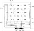
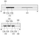
이하, 도 1 및 도 2를 참조하여 종래기술에 따른 정정용량 방식 터치 스크린 패널에 대하여 설명하기로 한다. 도 1은 종래의 기술에 따른 정전용량 방식의 터치 스크린 패널의 평면도이고, 도 2는 도 1에 도시된 터치 스크린 패널의 I-I'선 및 II-II'선을 따라 취한 단면도이다.1 and 2, a description will be made of a conventional touch screen panel of a capacitance type according to the related art. 1 is a plan view of a capacitive touch screen panel according to the related art, and FIG. 2 is a cross-sectional view taken along lines II ′ and II-II ′ of the touch screen panel illustrated in FIG. 1.
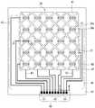
도 1 및 도 2를 참조하면, 종래의 정전용량 방식 터치 스크린 패널은 전극형성부(20), 라우팅 배선부(40), 패드부(60) 및 보호층(50)으로 이루어진다.1 and 2, the conventional capacitive touch screen panel includes an
전극형성부(20)는 기판(10) 상에 형성되며 제 1 방향(예컨대, X축 방향)으로 나란하게 배열된 복수의 제 1 전극들(21) 및 상기 제 1전극들(21)과 수직방향(예컨대, Y축 방향)으로 교차하여 배열되는 복수의 제 2 전극들(22)로 이루어 진다. 제 1 전극들(21)과 제 2 전극들(22)은 서로 교차하지만 절연층(30)에 의해 전기적으로 절연상태를 유지한다. 또한, 이웃하는 제 1 전극들(21)은 브릿지(41)에 의해 서로 연결된다. 즉, 브릿지(41)는 제 1 및 제 2 전극들(21, 22) 상부에 덮인 절연층(30)에 형성된 콘택홀들(30a , 30b)을 통해 이웃하는 제 1 전극들(21)을 상호 접속시킨다.The
라우팅 배선부(40)는 전극형성부(20)의 외곽에 형성되며 복수의 제 1 전극들(21)과 각각 연결되는 복수의 제 1 라우팅 배선들(42)과 복수의 제 2 전극들(22)과 각각 연결되는 복수의 제 2 라우팅 배선들(43)로 이루어 진다.The
패드부(60)는 복수의 제 1 라우팅 배선들(42)을 통해 복수의 제 1 전극들(21)과 각각 접속되는 복수의 제 1 패드들(61)과 복수의 제 2 라우팅 배선들(43)을 통해 복수의 제 2 전극들(22)과 각각 접속되는 복수의 제 2 패드들(62)로 이루어 진다.The
보호층(50)은 상기 전극형성부(20) 및 라우팅 배선부(40)를 커버하며, 제 1 및 제 2 전극들(21, 22)과 제 1 및 제 2 라우팅 배선들(42, 43)이 외부로 노출되는 것을 방지하여 준다.The
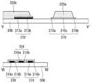
이하, 도 3a 내지 도 3d를 참조하여, 종래의 기술에 따른 정전용량 방식 터치 스크린 패널의 제조방법에 대해 설명하기로 한다.Hereinafter, a method of manufacturing a capacitive touch screen panel according to the related art will be described with reference to FIGS. 3A to 3D.
도 3a를 참조하면, 전극형성부, 라우팅 배선부 및 패드부를 구비하는 기판(10) 상에 스퍼터링 등의 증착공정을 통해 제 1 및 제 2 전극 형성용의 제 1 도전층을 전면 증착시킨다. 제 1 도전층으로서는 ITO층(Indium Tin Oxide 층)이 주로 사용된다. 제 1 도전층이 형성된 기판 상에 포토레지스트를 전면 도포한 후 제 1 마스크를 이용한 포토리소그래피 공정을 수행함으로써 전극형성부에 제 1 도전층을 노출시키는 제 1 포토레지스트 패턴을 형성한다. 그리고 제 1 포토레지스트 패턴에 의해 노출된 제 1 도전층을 습식 에칭(wet etching)을 통해 제거한 후 잔류하는 제 1 포토레지스트 패턴을 애싱함으로써, 기판(10)상에 복수의 제 1 전극들(21) 및 제 1 전극들과 교차하는 복수의 제 2 전극들(22)을 형성한다.Referring to FIG. 3A, the first conductive layers for forming the first and second electrodes are deposited on the entire surface of the
도 3b를 참조하면, 복수의 제 1 및 제 2 전극들(21, 22)이 형성된 기판(10) 상에 제 1 절연층(30)을 형성한 후, 제 2 마스크를 이용한 포토리소그래피 공정 및 식각공정으로 라우팅 배선부와 패드부의 제 1 절연층을 제거하고, 전극형성부의 제 1 절연층(30)을 관통하는 제 1 및 제 2 콘택홀들(30a, 30b)을 형성한다. 제 1 및 제 2 콘택홀들(30a, 30b)은 이웃하는 제 1 전극들(21)의 일부를 노출시킨다. 제 1 절연층(30)으로서는 실리콘 질화물, 실리콘 산화물, 또는 유기 수지 등이 사용될 수 있다.Referring to FIG. 3B, after forming the first
도 3c를 참조하면, 재 1 및 제 2 콘택홀(30a, 30b)이 형성된 기판의 전면 상에 스퍼터링 등의 증착공정을 통해 제 2 도전층을 형성한다. 제 2 도전층으로서는 알루미늄(Al) 또는 몰리브덴(Mo)이 사용될 수 있다. 제 2 도전층이 형성된 기판 상에 포토레지스트를 전면 도포한 후 제 3 마스크를 이용한 포토리소그래피 공정 및 식각 공정을 수행함으로써 기판(10)상의 라우팅부에는 제 1 및 제 2 라우팅 배선들(42, 43)이 형성되고, 전극형성부에는 제 1 절연층(30) 상에 연결전극(41)이 형성된다. 연결전극(41)은 제 1 절연층(30)에 형성된 제 1 및 제 2 콘택홀(30a, 30b)을 통해 분리된 제 1 전극들(21)을 연결하는 구성으로 된다.Referring to FIG. 3C, a second conductive layer is formed on the entire surface of the substrate on which the first and
도 3d를 참조하면, 연결전극(41)과 제 1 및 제 2 라우팅 배선들(42, 43)이 형성된 기판의 전면 상에 보호막으로서의 제 2 절연층(50)을 형성한 후, 제 4 마스크를 이용한 포토리소그래피 공정 및 식각공정으로 패드부의 제 1 및 제 2 라우팅 배선들(42, 43)이 노출되도록 제 2 절연층(50)을 관통하는 스루홀(50a)을 형성한다.Referring to FIG. 3D, after forming the second
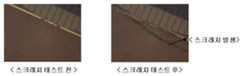
그러나, 종래기술에 따른 정전용량 방식 터치 스크린 패널은 상술한 바와 같이 4 마스크 공정으로 제조되고, 각 마스크 공정은 포토레지스트(photo resist: PR), 도포(coating), 정렬(alignmnet) 및 노광(exposure), 현상(developement), 세정(cleaning) 등의 일련의 연속공정을 필요로 하는 포토리소그래피(photolithography) 공정을 수반하므로, 마스크 공정을 절감하기 위한 필요성이 대두되었다. 또한 제 1 전극과 제 2 전극이 교차하는 부분의 제 1 절연층은 사용되는 면적이 넓고 실리콘 질화물, 실리콘 산화물, 유기 수지 등을 사용하기 때문에 주변과의 색감차로 인해 외측에서 시인되는 문제점이 있었다. 또한, 터치 스크린 패널의 최상단에 보호막으로서 형성된 제 2 절연층은 제 1 절연층과 동일한 재료를 사용하고 있고, 이들을 증착할 때 사용되는 가스에 의해 접착력이 악화되어 표면경도가 저하되는 문제가 있었다. 따라서, 터치 스크린 패널 제조 후, 표시장치를 형성하기 위한 후공정 진행시 스크래치 등의 불량이 발생하는 문제점이 있었다. 도 4는 종래 기술에 따라 제조된 터치 스크린 패널을 스크래치 테스트하기 전후의 상태를 각각 나타낸 도면으로서, 좌측 도면은 스크래치 테스트 전의 상태를, 우측 도면은 스크래치 테스트 후의 상태를 나타낸 도면이다.
However, the capacitive touch screen panel according to the prior art is manufactured in a four mask process as described above, each mask process is photo resist (PR), coating (coating), alignment and exposure (exposure) Since a photolithography process is required, which requires a series of continuous processes, such as development, cleaning, and the like, there is a need for reducing a mask process. In addition, since the first insulating layer at the portion where the first electrode and the second electrode intersect has a large area and uses silicon nitride, silicon oxide, organic resin, or the like, there is a problem that it is visually recognized from the outside due to color difference with the surroundings. In addition, the second insulating layer formed as a protective film on the top of the touch screen panel uses the same material as that of the first insulating layer, and there is a problem that the adhesive force is deteriorated due to the gas used to deposit them and the surface hardness is lowered. Therefore, after manufacturing the touch screen panel, there is a problem that a defect such as a scratch occurs during the post process for forming the display device. 4 is a view showing a state before and after a scratch test of a touch screen panel manufactured according to the prior art, the left side shows the state before the scratch test, the right side shows the state after the scratch test.
따라서, 본 발명의 목적은 정전용량 방식 터치 스크린 패널의 마스크 공정수를 절감하여 공정 택트타임(tact time)을 줄임으로써 생산성을 향상시키기 위한 것이다.Accordingly, an object of the present invention is to improve the productivity by reducing the number of mask processes of the capacitive touch screen panel to reduce the process tact time.
본 발명의 다른 목적은 터치전극으로 사용되는 제 1 전극과 제 2 전극을 커버하는 제 1 절연층의 면적이 넓고 주변과의 색감차로 인해 발생하는 시인성의 문제점을 해소시키고, 투과율 및 색전이 특성을 향상시키기 위한 것이다.Another object of the present invention is to solve the problem of visibility due to the wide area of the first insulating layer covering the first electrode and the second electrode used as the touch electrode and the color difference with the surroundings, and to improve the transmittance and color transition characteristics. It is to improve.
본 발명의 또 다른 목적은 터치 스크린 패널의 최상단에 보호막으로 형성된 제 2 절연층의 표면경도가 낮아서 발생하는 스크래치 문제점을 해소시키기 위한 것이다.
Another object of the present invention is to solve the scratch problem caused by the low surface hardness of the second insulating layer formed as a protective film on the top of the touch screen panel.
상기 목적을 달성하기 위하여, 본 발명의 제 1 특징에 따른 정전용량 방식 터치 스크린 패널은, 기판; 상기 기판 상의 전극 형성부에 형성되는 복수의 제 1 연결패턴들; 상기 전극 형성부의 외곽부에 형성되는 상기 기판 상의 라우팅 배선부에서 상기 제 1 연결패턴과 동일 평면 상에 형성되는 복수의 제 1 라우팅 배선들과 복수의 제 2 라우팅 배선들; 상기 복수의 제 1 연결패턴들을 커버하도록 상기 기판 상에 형성되며 적어도 2개의 콘택홀을 갖는 절연층; 및 상기 절연층 상에 제 1 방향으로 평행하게 배열되며, 상기 복수의 제 1 라우팅 배선들과 접속되는 복수의 제 1 전극패턴들 및 상기 복수의 제 1 전극패턴들과 교차하는 제 2 방향으로 평행하게 배열되며, 상기 복수의 제 2 라우팅 배선들과 접속되는 복수의 제 2 전극패턴들을 포함하며, 상기 복수의 제 1 연결패턴들의 각각은 상기 제 1 연결패턴의 부분들을 노출시키는 상기 적어도 2개의 콘택홀을 통해 상기 복수의 제 1 전극패턴들의 인접한 쌍을 서로 접속시키는 것을 특징으로 한다.In order to achieve the above object, a capacitive touch screen panel according to a first aspect of the present invention, the substrate; A plurality of first connection patterns formed on an electrode forming portion on the substrate; A plurality of first routing wires and a plurality of second routing wires formed on the same plane as the first connection pattern in a routing wire part on the substrate formed at an outer portion of the electrode forming part; An insulating layer formed on the substrate to cover the plurality of first connection patterns and having at least two contact holes; And a plurality of first electrode patterns arranged in parallel in a first direction on the insulating layer and connected to the plurality of first routing lines, and in a second direction crossing the plurality of first electrode patterns. And a plurality of second electrode patterns connected to the plurality of second routing wires, each of the plurality of first connection patterns exposing portions of the first connection pattern. Adjacent pairs of the plurality of first electrode patterns are connected to each other through a hole.
또한, 본 발명의 제 2 특징에 따른 정전용량 방식 터치 스크린 패널은, 기판; 상기 기판 상에 제 1 방향으로 나란하게 배열되는 복수의 제 1 전극열들과, 상기 제 1 전극열들과 교차하도록 배열되는 복수의 제 2 전극열들을 포함하는 전극 형성부; 상기 전극 형성부의 외곽부에서 상기 기판 상에 형성되며, 상기 복수의 제 1 전극열들과 각각 연결되는 복수의 제 1 라우팅 배선들과, 상기 복수의 제 2 전극열들과 각각 연결되는 복수의 제 2 라우팅 배선들을 포함하는 라우팅 배선부; 상기 복수의 제 1 및 제 2 라우팅 배선들과 동일층에 형성되며, 서로 분리되어 형성되는 복수의 제 1 연결패턴들; 및 상기 제 1 전극열과 상기 제 2 전극열이 교차하는 곳에서 상기 제 1 전극열과 상기 제 2 전극열을 절연시키는 절연층을 포함하며, 상기 복수의 제 1 전극열들의 각각은 서로 분리된 복수의 제 1 전극패턴들을 포함하고, 상기 제 1 전극패턴들의 인접한 쌍은 상기 제 1 연결패턴에 의해 접속되는 것을 특징으로 한다.In addition, the capacitive touch screen panel according to the second aspect of the present invention, the substrate; An electrode forming unit including a plurality of first electrode rows arranged side by side in a first direction on the substrate and a plurality of second electrode rows arranged to intersect the first electrode rows; A plurality of first routing wires formed on the substrate at an outer portion of the electrode forming unit, respectively connected to the plurality of first electrode rows, and connected to the plurality of second electrode rows, respectively; A routing wiring unit including two routing wirings; A plurality of first connection patterns formed on the same layer as the plurality of first and second routing lines and separated from each other; And an insulating layer which insulates the first electrode string and the second electrode string from where the first electrode string and the second electrode string intersect, each of the plurality of first electrode strings being separated from each other. And first electrode patterns, and adjacent pairs of the first electrode patterns are connected by the first connection pattern.
또한, 본 발명의 특징에 따른 정전용량 방식 터치 스크린 패널의 제조방법은, 기판 상에 복수의 제 1 연결패턴들, 복수의 제 1 라우팅 배선들 및 복수의 제 2 라운팅 배선들을 포함하는 제 1 도전성 패턴을 형성하는 제 1 공정; 상기 제 1 도전성 패턴이 형성된 상기 기판의 전면에 절연층을 형성하고, 상기 절연층을 패터닝하여 상기 제 1 연결패턴의 양단부를 노출시키는 제 1 절연패턴과 상기 제 1 라우팅 배선의 일부 및 상기 제 2 라우팅 배선의 일부를 노출시키는 제 2 절연패턴을 형성하는 제 2 공정; 및 상기 제 1 및 제 2 절연패턴이 형성된 상기 기판 상에 제 2 도전층을 형성한 후, 상기 제 2 도전층을 패터닝하여 제 1 방향으로 평행하게 배열되는 복수의 제 1 전극열들과, 상기 제 1 방향과 교차하는 제 2 방향으로 평행하게 배열되는 복수의 제 2 전극열들을 포함하는 제 2 도전성 패턴을 형성하는 제 3 공정을 포함하며, 상기 복수의 제 1 전극열들의 각각은 서로 분리된 복수의 제 1 전극패턴들을 포함하고, 상기 제 1 전극패턴들의 인접한 쌍은 상기 제 1 연결패턴에 의해 접속되는 것을 특징으로 한다.
In addition, a method of manufacturing a capacitive touch screen panel according to an aspect of the present invention includes a first including a plurality of first connection patterns, a plurality of first routing wires, and a plurality of second routing wires on a substrate. A first step of forming a conductive pattern; An insulating layer is formed on the entire surface of the substrate on which the first conductive pattern is formed, and the first insulating pattern and a part of the first routing wire and the second insulating pattern exposing both ends of the first connection pattern by patterning the insulating layer. A second process of forming a second insulating pattern exposing a part of the routing wiring; And forming a second conductive layer on the substrate on which the first and second insulating patterns are formed, and then patterning the second conductive layer to form a plurality of first electrode rows arranged in parallel in a first direction. And forming a second conductive pattern including a plurality of second electrode rows arranged in parallel in a second direction crossing the first direction, wherein each of the plurality of first electrode rows is separated from each other. And a plurality of first electrode patterns, and adjacent pairs of the first electrode patterns are connected by the first connection pattern.
본 발명의 제 1 및 제 2 실시예에 따른 정전용량 방식 터치 스크린 패널 및 그 제조방법에 따르면, 동일한 공정을 통해 제 1 연결패턴들과 제 1 및 제 2 라우팅 배선들이 형성되기 때문에 적어도 하나의 마스크 공정을 생략할 수 있다. 따라서, 마스크수 절감에 따른 비용절감 및 택트타임(tact time)을 줄일 수 있는 효과를 얻을 수 있다.According to the capacitive touch screen panel and the manufacturing method thereof according to the first and second embodiments of the present invention, at least one mask is formed because the first connection patterns and the first and second routing wires are formed through the same process. The process can be omitted. Therefore, the cost reduction and the tact time according to the reduction of the number of masks can be obtained.
또한, 본 발명에서는 절연층으로서 규소질화물(SiNx)을 이용하기 때문에 주변과의 색감차로 인해 발생하는 시인성의 문제점을 해소할 수 있고, 그 두께를 5,000Å~7,000Å의 범위로 사용하고 있기 때문에, 투과율이 최대로 되고 색전이 현상이 최소로 될 뿐 아니라 절연층이 파괴되는 현상을 억제할 수 있다. 따라서, 터치 스크린 패널의 안정성이 현저히 개선되는 효과를 얻을 수 있다.In addition, in the present invention, since silicon nitride (SiNx) is used as the insulating layer, the problem of visibility caused by color difference with the surroundings can be solved, and the thickness is used in the range of 5,000 kPa to 7,000 kPa, The transmittance is maximized, the color transition phenomenon is minimized, and the phenomenon that the insulating layer is destroyed can be suppressed. Therefore, the effect of remarkably improving the stability of the touch screen panel can be obtained.
또한, 본 발명에서는 터치 스크린 패널의 최상위층에 형성되는 제 1 및 제 2 전극열들과 제 2 연결패턴들을 경도가 높은 ITO를 이용하기 때문에, 터치 스크린 패널과 기판을 공통으로 사용할 수 있는 표시장치에 응용할 경우 후공정에서 스크래치가 발생하지 않는 효과를 얻을 수 있다. 또한, ITO의 두께를 1200Å~1600Å로 하면 투과율을 최대로 하는 효과를 얻을 수가 있다In addition, in the present invention, since the first and second electrode strings and the second connection patterns formed on the uppermost layer of the touch screen panel use ITO having high hardness, the display device can use the touch screen panel and the substrate in common. If applied, the scratch-free effect can be obtained in the post process. In addition, when the thickness of the ITO is 1200 kPa to 1600 kPa, the effect of maximizing the transmittance can be obtained.
또한, 절연층 하부에 형성되어 제 1 전극패턴들을 연결하는 제 1 연결패턴의 두께를 2000Å~3000Å로 함으로써 양호한 공정성과 적절한 저항값을 얻을 수 있으며, 폭을 3㎛~10㎛의 범위로 함으로써 패턴이 시인되지 않는 효과를 달성할 수 있다.In addition, a good processability and an appropriate resistance value can be obtained by setting the thickness of the first connection pattern formed under the insulating layer to connect the first electrode patterns to 2000 kPa to 3000 kPa, and the width of 3 m to 10 m. This invisible effect can be achieved.
도 1은 종래의 기술에 따른 정전용량 방식의 터치 스크린 패널의 평면도,
도 2는 도 1에 도시된 터치 스크린 패널의 I-I'선 및 II-II'선을 따라 취한 단면도,
도 3a 내지 도 3d는 도 1에 도시된 종래의 기술에 따른 터치 스크린 패널의 제조 공정을 도시한 단면도,
도 4는 종래 기술에 따른 터치 스크린 패널을 스크래치 테스트하기 전후의 상태를 각각 나타낸 도면,
도 5는 본 발명의 제 1 실시예에 따른 터치 스크린 패널의 평면도,
도 6은 도 5에 도시된 본 발명의 제 1 실시예에 따른 터치 스크린 패널의 I-I'선 및 II-II'선을 따라 취한 단면도,
도 7a 내지 도 7b는 도 5에 도시된 본 발명의 제 1 실시예에 따른 터치 스크린 패널의 제조 공정 중 제 1 마스크 공정을 도시한 평면도 및 단면도,
도 8a 내지 도 8d는 도 5에 도시된 본 발명의 제 1 실시예에 따른 터치 스크린 패널의 제조 공정 중 제 2 마스크 공정을 도시한 평면도 및 단면도,
도 9a 및 도 9b는 도 5에 도시된 본 발명의 제 1 실시예에 따른 터치 스크린 패널의 제조 공정 중 제 3 마스크 공정을 도시한 평면도 및 단면도,
도 9c는 도 5에 도시된 본 발명의 제 1 실시예에 따른 터치 스크린 패널의 제조 공정 중 제 2 및 제 3 마스크 공정 후 얻어지는 다른 실시예의 터치 스크린 패널의 단면도를 도시한 도면이다.
도 10은 본 발명의 제 2 실시예에 따른 터치 스크린 패널의 평면도,
도 11은 도 10에 도시된 본 발명의 제2 실시예에 따른 터치 스크린 패널의 III-III'선 및 IV-IV'선을 따라 취한 단면도,
도 12a 내지 도 12b는 도 10에 도시된 본 발명의 제 2 실시예에 따른 터치 스크린 패널의 제조 공정 중 제 1 마스크 공정을 도시한 평면도 및 단면도,
도 13a 내지 도 13d는 도 10에 도시된 본 발명의 제 2 실시예에 따른 터치 스크린 패널의 제조 공정 중 제 2 마스크 공정을 도시한 평면도 및 단면도,
도 14a 및 도 14b는 도 10에 도시된 본 발명의 제 2 실시예에 따른 터치 스크린 패널의 제조 공정 중 제 3 마스크 공정을 도시한 평면도 및 단면도,
도 15는 본 발명의 제 3 실시예에 따른 터치 스크린 패널의 평면도,
도 16은 도 15에 도시된 본 발명의 제 3 실시예에 따른 터치 스크린 패널의 V-V'선 및 VI-VI'선을 따라 취한 단면도,
도 17a 내지 도 17b는 도 15에 도시된 본 발명의 제 3 실시예에 따른 터치 스크린 패널의 제조 공정 중 제 1 마스크 공정을 도시한 평면도 및 단면도,
도 18a 내지 도 18b는 도 10에 도시된 본 발명의 제 3 실시예에 따른 터치 스크린 패널의 제조 공정 중 제 2 마스크 공정을 도시한 평면도 및 단면도,
도 19a 내지 도 19d는 도 10에 도시된 본 발명의 제 3 실시예에 따른 터치 스크린 패널의 제조 공정 중 제 3 마스크 공정을 도시한 평면도 및 단면도,
도 20a 내지 도 20c는 도 15에 도시된 본 발명의 제 3 실시예에 따른 터치 스크린 패널의 제조 공정 중 제 4 마스크 공정을 도시한 평면도 및 단면도,
도 21은 제 1 및 제 2 전극패턴들로 이용한 ITO의 두께를 1,400Å으로 형성하였을 경우, 절연층으로서 이용된 실리콘 질화물의 두께에 따른 절연층의 파괴되거나 손상되는 항복점의 전계값을 나타낸 그래프,
도 22는 제 1 및 제 2 전극패턴들로 이용한 ITO의 두께를 1,400Å으로 형성하였을 경우, 절연층으로서 이용된 실리콘 질화물의 두께에 따른 터치 스크린 패널의 투과율을 나타낸 그래프,
도 23은 제 1 및 제 2 전극패턴들로 이용한 ITO의 두께를 1,400Å으로 형성하였을 경우, 절연층으로서 이용된 실리콘 질화물의 두께에 따른 터치 스크린 패널의 색전이 특성을 나타낸 그래프
도 24는 절연층으로서 형성한 실리콘 질화물의 두께를 6,000Å으로 형성하였을 경우, 제 1 및 제 2 전극패턴들로 이용한 ITO의 두께에 따른 투과율의 특성을 도시한 그래프,
도 25는 절연층으로서 형성한 실리콘 질화물의 두께를 6,000Å으로 형성하였을 경우, 제 1 및 제 2 전극패턴들로 이용한 ITO의 두께에 따른 색전이 특성을 도시한 그래프,
도 26은 터치 스크린 패널의 최상단이 절연층인 영역 A와 ITO인 영역 B에 대한 스크래치 테스트 전과, 테스트 후의 결과를 나타낸 도면.
FIG. 1 is a plan view of a capacitive touch screen panel according to the related art,
FIG. 2 is a cross-sectional view taken along lines II ′ and II-II ′ of the touch screen panel illustrated in FIG. 1;
3A to 3D are cross-sectional views illustrating a manufacturing process of a touch screen panel according to the related art shown in FIG. 1,
4 is a view showing a state before and after each scratch test the touch screen panel according to the prior art,
5 is a plan view of a touch screen panel according to a first embodiment of the present invention;
6 is a cross-sectional view taken along lines II ′ and II-II ′ of the touch screen panel according to the first embodiment of the present invention illustrated in FIG. 5;
7A to 7B are plan views and cross-sectional views illustrating a first mask process during a manufacturing process of the touch screen panel according to the first embodiment of the present invention shown in FIG. 5;
8A to 8D are plan views and cross-sectional views illustrating a second mask process during the manufacturing process of the touch screen panel according to the first embodiment of the present invention shown in FIG. 5;
9A and 9B are plan views and cross-sectional views illustrating a third mask process during the manufacturing process of the touch screen panel according to the first embodiment of the present invention shown in FIG. 5;
FIG. 9C is a cross-sectional view of another embodiment of the touch screen panel obtained after the second and third mask processes in the manufacturing process of the touch screen panel according to the first embodiment of FIG. 5.
10 is a plan view of a touch screen panel according to a second embodiment of the present invention;
FIG. 11 is a cross-sectional view taken along lines III-III ′ and IV-IV ′ of the touch screen panel according to the second embodiment of the present invention shown in FIG. 10;
12A to 12B are plan views and cross-sectional views illustrating a first mask process during a manufacturing process of a touch screen panel according to a second embodiment of the present invention shown in FIG. 10;
13A to 13D are plan views and cross-sectional views illustrating a second mask process during the manufacturing process of the touch screen panel according to the second embodiment of the present invention shown in FIG. 10;
14A and 14B are plan views and cross-sectional views illustrating a third mask process during the manufacturing process of the touch screen panel according to the second embodiment of the present invention shown in FIG. 10;
15 is a plan view of a touch screen panel according to a third embodiment of the present invention;
FIG. 16 is a cross-sectional view taken along lines V-V ′ and VI-VI ′ of the touch screen panel according to the third embodiment of the present invention shown in FIG. 15;
17A to 17B are plan views and cross-sectional views illustrating a first mask process during a manufacturing process of a touch screen panel according to a third embodiment of the present invention shown in FIG. 15;
18A to 18B are plan views and cross-sectional views illustrating a second mask process during the manufacturing process of the touch screen panel according to the third embodiment of the present invention shown in FIG. 10;
19A to 19D are plan views and cross-sectional views illustrating a third mask process during the manufacturing process of the touch screen panel according to the third embodiment of the present invention shown in FIG. 10;
20A to 20C are plan views and cross-sectional views illustrating a fourth mask process during the manufacturing process of the touch screen panel according to the third embodiment of the present invention shown in FIG. 15;
21 is a graph showing the electric field value of the breakdown or damage point of the insulating layer according to the thickness of the silicon nitride used as the insulating layer when the thickness of ITO used as the first and second electrode patterns is 1,400 kPa;
22 is a graph showing the transmittance of a touch screen panel according to the thickness of silicon nitride used as an insulating layer when the thickness of ITO used as the first and second electrode patterns is 1,400 kPa;
FIG. 23 is a graph illustrating color transition characteristics of a touch screen panel according to a thickness of silicon nitride used as an insulating layer when the thickness of ITO used as the first and second electrode patterns is 1,400 kPa.
24 is a graph showing the characteristics of transmittance according to the thickness of ITO used as the first and second electrode patterns when the thickness of the silicon nitride formed as the insulating layer is 6,000 kPa;
FIG. 25 is a graph illustrating the color transition characteristics according to the thickness of ITO used as the first and second electrode patterns when the thickness of the silicon nitride formed as the insulating layer is 6,000 kPa;
Fig. 26 shows the results before and after the scratch test for the region A, which is the insulating layer, and the region B, which is the ITO, at the top of the touch screen panel;
이하, 첨부도면을 참조하여 본 발명의 바람직한 실시예에 대하여 상세히 설명하기로 한다. 명세서 전체에 걸쳐 동일 참조 부호는 동일 구성 요소를 나타낸다.Hereinafter, preferred embodiments of the present invention will be described in detail with reference to the accompanying drawings. Like reference numerals refer to like elements throughout the specification.
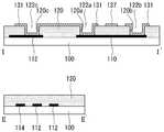
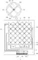
우선, 도 5 및 도 6을 참조하여 본 발명의 제 1 실시예에 따른 액정표시장치용 어레이 기판에 대해 설명하기로 한다. 도 5는 본 발명의 제 1 실시예에 따른 터치 스크린 패널의 평면도, 도 6은 도 5에 도시된 본 발명의 제 1 실시예에 따른 터치 스크린 패널의 I-I'선 및 II-II'선을 따라 취한 단면도이다.First, an array substrate for a liquid crystal display device according to a first embodiment of the present invention will be described with reference to FIGS. 5 and 6. 5 is a plan view of a touch screen panel according to a first exemplary embodiment of the present invention, and FIG. 6 is a line II ′ and II-II ′ of a touch screen panel according to the first exemplary embodiment of the present invention illustrated in FIG. 5. It is a cross-sectional view taken along.
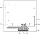
도 5 및 도 6을 참조하면, 본 발명의 제 1 실시예에 따른 정전용량 방식 터치 스크린 패널은 전극형성부(A), 라우팅 배선부(B) 및 패드부(C)를 포함한다.5 and 6, the capacitive touch screen panel according to the first embodiment of the present invention includes an electrode forming portion A, a routing wiring portion B, and a pad portion C.
전극형성부(A)는 제 1 방향(예컨대, X축 방향)으로 나란하게 배열된 복수의 제 1 전극열들(130)과 상기 제 1 전극열들(130)과 교차하는 제 2 방향(예컨대, Y축 방향)으로 배열되는 복수의 제 2 전극열들(135)을 포함한다. 제 1 전극열들(130)의 각각은 삼각형, 사각형, 마름모꼴, 다각형 등으로 형성된 제 1 전극패턴들(131)과 이들 제 1 전극패턴들(131)을 연결하는 제 1 연결패턴들(110)을 포함한다. 제 2 전극열들(135)의 각각 또한 제 1 전극패턴들(131)과 유사한 삼각형, 사각형, 마름모꼴, 다각형 등으로 형성된 제 2 전극패턴들(136)과 이들 제 2 전극패턴들(136)을 서로 연결하는 제 2 연결패턴들(137)을 포함한다.The electrode forming part A may have a plurality of
본 발명의 제 1 실시예에서는 제 1 연결패턴들(110)은 제 1 전극패턴들(131)과 별도로 형성되며, 제 2 연결패턴들(137)은 제 2 전극패턴들(136)과 일체로 형성된다. 그러나, 그와 반대로 제 1 연결패턴들(110)은 제 1 전극패턴들(131)과 일체로 형성되고, 제 2 연결패턴들(137)은 제 2 전극패턴들(136)과 별도로 형성되도록 구성할 수도 있다.In the first embodiment of the present invention, the
라우팅 배선부(B)는 전극형성부(A)의 외곽부에 형성되며 복수의 제 1 전극열들(130)과 각각 연결되는 복수의 제 1 라우팅 배선들(112)과 복수의 제 2 전극열들(135)과 각각 연결되는 복수의 제 2 라우팅 배선들(114)로 이루어 진다.The routing wiring part B is formed at an outer portion of the electrode forming part A, and the plurality of
패드부(C)는 복수의 제 1 라우팅 배선들(112)을 통해 복수의 제 1 전극열들(130)과 각각 접속되는 복수의 제 1 패드들(116)과 복수의 제 2 라우팅 배선들(114)을 통해 복수의 제 2 전극열들(135)과 각각 접속되는 복수의 제 2 패드들(118)로 이루어 진다.The pad part C may include a plurality of
한편, 본 발명의 제 1 실시예에서는 제 1 연결패턴들(110)과 제 1 및 제 2 라우팅 배선들(112, 114)은 동일 공정을 통해 기판(100) 상에 형성되며, 동일물질을 이용하여 형성된다. 그러나, 제 1 연결패턴들(110)과 제 1 및 제 2 라우팅 배선들(112, 114)은 상이한 물질로 형성될 수도 있다. 제 1 연결패턴들(110)과 제 1 및 제 2 라우팅 배선들(112, 114)을 형성하는 재료로는 Al, AlNd, Mo, MoTi, Cu, Cr 등이 이용된다. 이들 재료는 비저항이 낮은 물질이기 때문에 전극 연결부위의 저항을 낮추는 효과가 있다. ITO(Indium Tin Oxide)는 비저항이 높기 때문에 두께를 두껍게 해야 하는 문제점이 있기는 하지만, 비저항이 낮은 다른 금속과 함께 사용될 수도 있다. 또한, 제 1 연결패턴들(110)은 2000Å~3000Å의 두께를 가지며, 3㎛~10㎛의 폭을 가지도록 형성하는 것이 바람직하다. 제 1 연결패턴들(110)의 두께가 2000Å미만일 경우에는 저항이 높아지고, 3000Å이상일 때에는 패턴의 단차가 심해지는 문제가 있으며, 제 1 연결패턴들(110)의 폭이 3㎛미만일 때에는 저항이 높아지고, 10㎛보다 클 경우에는 패턴이 시인되는 문제점이 있기 때문이다.Meanwhile, in the first embodiment of the present invention, the
또한, 본 발명의 제 1 실시예에 따른 제 1 연결패턴들(110)과 제 1 및 제 2 라우팅 배선들(112, 114)은 동일 공정을 통해 형성되기 때문에 전극패턴들을 연결하는 연결패턴과 라우팅 배선을 서로 상이한 공정에서 형성하는 종래기술에 비해 하나의 마스크 공정을 생략할 수 있어 비용절감 및 택트타임(tact time: 일간 생산목표량을 달성하기 위한 제품단위당 제작 소요시간)을 줄일 수 있는 효과도 얻을 수 있다.In addition, since the
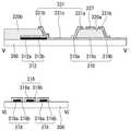
본 발명의 제 1 실시예에서는 제 1 연결패턴들(110)과 제 1 및 제 2 라우팅 배선들(112, 114)이 형성된 기판(100) 상에는 전면적으로 절연층(120)이 형성되고, 절연층(120)에는 제 1 연결패턴들(110) 각각의 일부분들을 노출시키는 제 1 및 제 2 콘택홀들(120a, 120b)과, 제 1 라우팅 배선들(112)의 일부를 노출시키는 제 3 콘택홀(120c) 및 제 2 라우팅 배선들(114)의 일부를 노출시키는 제 4 콘택홀(120d, 도 8a 참조)이 형성된다. 절연층(120)의 재료로는 질화실리콘(SiNx)이 이용된다. 절연층(120)의 두께는 5,000Å 미만의 경우에는 제 1 전극열(130)과 제 2 전극열(135)에 걸리는 전압에 의해 절연층(120)이 파괴되거나 손상될 수 있다. 따라서, 터치 스크린 패널의 사용중에 절연층(120)이 파괴되거나 손상되어 고장이 발생하는 현상을 방지하기 위해서는 절연층(120)의 두께를 5,000Å 이상으로 하는 것이 바람직하다. 또한, 절연층(120)의 두께가 6,000Å 부근에서는 투과율이 더 이상 증가하지 않는 포화상태를 나타내고 색전이 현상 또한 최소로 된다. 즉, 투과율과 색도표현의 측면에서는 절연층(120)의 두께가 6,000Å 이상일 때 투과율이 최대로 되고 색전이 현상도 최소로 되기 때문에 가장 바람직하다. 그러나, 절연층의 두께가 7,000Å를 초과하면 절연층의 재료로 이용되는 질화실리콘막의 특성상 콘택홀의 형성이 어려워지고 공정시간이 많이 소요되므로 바람직하지 못하다. 따라서, 절연층의 안정성과 양호한 광투과율 및 색도표현 능력을 종합해 보았을 때 절연층(120)의 두께를 5,000Å~7,000Å의 범위로 하는 것이 바람직하다.In the first embodiment of the present invention, the insulating
또한, 제 1 내지 제 4 콘택홀들(120a, 120b, 120c, 120d)이 형성된 절연층(120) 상에는 복수의 제 1 전극패턴들(131)로 구성되며 제 1 방향(예를 들면, x축 방향)으로 배열되는 복수의 제 1 전극열들(130)이 형성되고, 복수의 제 2 전극패턴들(136)로 구성되며 제 1 방향과 교차하는 제 2 방향(예를 들면, y축 방향)으로 배열되는 복수의 제 2 전극열들(135)이 형성된다. 제 1 전극열(130)을 구성하는 제 1 전극패턴들(131)은 서로 분리되어 형성되기 때문에 절연층(120)에 형성된 제 1 및 제 2 콘택홀들(120a, 120b)을 통해 절연층(120) 하부에 형성된 제 1 연결패턴(110)에 의해 접속되며, 최외각에 위치된 제 1 전극패턴들(131)은 제 3 콘택홀(120c)을 통해 제 1 라우팅 배선들(112)과 접속된다.In addition, on the insulating
도 6에 도시된 바와 같이, 복수의 제 1 전극패턴들(131)의 각각의 일부분은 제 1 내지 제 3 콘택홀들(120a, 120b, 120c) 내에 부분적으로 채워지도록 형성된다. 예컨대, 상기 제 1 전극패턴(131)의 일부분은 제 1 내지 제 3 콘택홀들(120a, 120b, 120c)의 측벽과 제 1 연결패턴(110) 및 제 1 라우팅 배선(112)의 노출부 상에 형성된다. 따라서, 제 1 내지 제 3 콘택홀들(120a, 120b, 120c) 내에 부분적으로 채워진 상기 제 1 전극패턴(131)의 부분에 의해 제 1 내지 제 3 콘택홀들(120a, 120b, 120c) 상부에는 각각 제 1 내지 제 3 오목부(122a, 122b, 122c)가 형성된다.As shown in FIG. 6, a portion of each of the plurality of
반면 제 2 전극열(135)을 구성하는 제 2 전극패턴들(136)은 제 2 연결패턴들(137)과 일체로 형성되며, 제 4 콘택홀(120d, 도 8a 참조)을 통해 제 2 라우팅 배선들(114)과 접속된다. 제 1 및 제 2 전극패턴들(131, 136)과 제 2 연결패턴들(137)은 동일 공정을 통해 동일 재료로 형성된다. 제 1 및 제 2 전극패턴들(131, 136)과 제 2 연결패턴들(137)의 재료로는 ITO가 이용된다. 본 발명의 실시예에서는 터치 스크린 패널의 최상위층에 ITO를 이용한 제 1 및 제 2 전극열들(130, 135)과 제 2 연결패턴들(137)이 형성되고, ITO는 경도가 높기 때문에 터치 스크린 패널의 기판(100)의 다른 면에 표시장치를 형성하기 위한 후공정에서 스크래치가 발생하지 않게 되어 양호한 품질의 터치 스크린 패널이 얻어진다.On the other hand, the
이하, 도 7a 내지 도 9c를 참조하여, 본 발명의 제 1 실시예에 따른 정전용량 방식 터치 스크린 패널의 제조방법에 대해 설명하기로 한다.Hereinafter, a method of manufacturing a capacitive touch screen panel according to a first embodiment of the present invention will be described with reference to FIGS. 7A to 9C.
도 7a 및 도 7b는 본 발명의 제 1 실시예에 따르는 정전용량 방식 터치 스크린 패널의 제조방법 중 제 1 마스크 공정을 설명하기 위한 평면도 및 단면도이다.7A and 7B are plan and cross-sectional views illustrating a first mask process in the method of manufacturing the capacitive touch screen panel according to the first embodiment of the present invention.
도 5, 도 7a 및 도 7b를 참조하면, 제 1 마스크 공정을 이용하여 전극형성부(A), 라우팅 배선부(B) 및 패드부(C)를 구비하는 기판(100) 상에 제 1 연결패턴(110), 제 1 라우팅 배선(112) 및 제 2 라우팅 배선(114)을 포함하는 제 1 도전성 패턴군이 형성된다.5, 7A, and 7B, a first connection is performed on a
이를 보다 상세히 설명하면, 기판(100) 상에 스퍼터링 등의 증착공정을 통해 제 1 도전층이 전면증착된다. 그리고, 제 1 마스크를 이용한 포토리소그래피 공정과 식각공정으로 제 1 도전층이 패터닝됨으로써 제 1 연결패턴들(110), 제 1 라우팅 배선들(112) 및 제 2 라우팅 배선들(114)을 포함하는 제 1 도전성 패턴군이 형성된다. 여기에서 제 1 도전성 패턴군을 형성하는 재료로는 Al, AlNd, Mo, MoTi, Cu, Cr, ITO(Indium Tin Oxide) 등이 이용된다. 제 1 도전성 패턴군 중 전극형성부(A, 도 5 참조)에 형성되는 제 1 연결패턴(110)의 두께는 2000Å~3000Å의 범위로, 폭은 3㎛~10㎛의 범위를 갖도록 형성된다.In more detail, the first conductive layer is entirely deposited on the
한편, 제 1 연결패턴(110), 제 1 라우팅 배선(112) 및 제 2 라우팅 배선(114)를 포함하는 제 1 도전성 패턴군은 기판(100) 상에 프린팅 방법으로 형성한 후, 건조 및 가열하여 형성할 수도 있다. 이 경우, 제 1 마스크 공정을 이용한 포토리소그래피 공정 및 에칭공정을 생략할 수 있게 된다. 제 1 도전성 패턴군은 인쇄법 외의 다른 패턴형성 방법을 이용하여 형성할 수도 있다.Meanwhile, the first conductive pattern group including the
도 8a 및 도 8d는 본 발명의 제 1 실시예에 따르는 정전용량 방식 터치 스크린 패널의 제조방법 중 제 2 마스크 공정을 설명하기 위한 평면도 및 단면도이다. 도 8a에서 점선으로 표시된 제 1 및 제 2 라우팅 배선들(112, 114)은 절연층(120)으로 덮여 있기 때문에 실질적으로는 평면도 상에서는 보이지 않는 부분이지만, 본 발명에서는 이해를 돕기 위해 점선으로 표시하였다.8A and 8D are plan views and cross-sectional views illustrating a second mask process in the method of manufacturing the capacitive touch screen panel according to the first embodiment of the present invention. Although the first and
도 8a 및 도 8b를 참조하면, 제 1 연결패턴(110), 제 1 라우팅 배선(112) 및 제 2 라우팅 배선(114)을 포함하는 제 1 도전성 패턴군이 형성된 기판(100) 상의 전면에 스퍼터링 등의 증착방법을 통해 절연층(120)이 형성된다. 절연층(120)의 재료로는 질화 실리콘(SiNx) 등의 무기 절연물질이 이용된다. 절연층(120)의 두께는 바람직하게는 5,000Å~10,000Å의 범위로, 더욱 바람직하게는 5,000Å~7,000Å의 범위로 설정한다.8A and 8B, sputtering is performed on the entire surface of the
절연층(120)이 형성된 후, 도 8c에 도시된 바와 같이 제 2 마스크를 이용한 포토리소그래피 공정을 이용하여, 절연층(120)이 존재해야 하는 부분에 포토레지스트 패턴(1000)이 형성된다. 그리고, 포토레지스트 패턴(1000)을 이용한 건식 식각공정으로 절연층(120)을 관통하는 제 1 내지 제 4 콘택홀(120a, 120b, 120c, 120d)이 형성된다. 그 다음 포토레지스트 패턴(1000)이 제거됨으로써 도 8d에 도시된 바와 같이 절연층(120) 하부에 형성된 제 1 전극패턴(110, 112, 114)을 노출시키는 제 1 내지 제 4 콘택홀(120a, 120b, 120c, 120d)이 형성된다. 여기에서, 제 1 콘택홀(120a)은 제 1 연결패턴(110)의 일부를, 제 2 콘택홀(120b)은 제 1 연결패턴(110)의 다른 일부를, 제 3 콘택홀(120c)은 제 1 라우팅 배선(112)의 일부를, 제 4 콘택홀(120d)(도 8A 참조)은 제 2 라우팅 배선(114)의 일부를 각각 노출시킨다.After the insulating
한편, 본 발명의 제 1 실시예에서는 제 1 내지 제 4 콘택홀(120a, 120b, 120c), 120d)의 단면 형상이 도 8A에 도시된 바와 같이 장방형인 것으로 되어 있으나, 본 발명이 이에 한정되는 것은 아니며, 원형, 타원형, 다각형 또는 불규칙한 형상과 같은 다른 임의의 형상을 포함할 수 있다. 또한, 제 1 내지 제 3 오목부들(122a, 122b, 122c)은 절연층(120)의 두께와 제 1 및 제 2 전극패턴의 두께에 따라 약 2,000Å~9,000Å의 깊이를 가질 수 있다.Meanwhile, in the first embodiment of the present invention, the cross-sectional shapes of the first to
도 9a 및 도 9b는 본 발명의 제 1 실시예에 따르는 정전용량 방식 터치 스크린 패널의 제조방법 중 제 3 마스크 공정을 설명하기 위한 평면도 및 단면도이다. 도 9a는 본 발명의 제 1 실시예에 따르는 정전용량 방식 터치 스크린 패널의 제조방법 중 제 3 마스크 공정에 의해 형성된 평면도를 도시한 도면으로서, 이해를 돕기 위해 제 1 도전성 패턴군과 제 2 도전성 패턴군 사이에 형성된 절연층(120)을 생략한 도면이다.9A and 9B are plan and cross-sectional views illustrating a third mask process in the method of manufacturing the capacitive touch screen panel according to the first embodiment of the present invention. FIG. 9A illustrates a plan view formed by a third mask process in a method of manufacturing a capacitive touch screen panel according to a first embodiment of the present invention. FIG. 9A illustrates a first conductive pattern group and a second conductive pattern for better understanding. The insulating
도 9a 및 도 9b를 참조하면, 제 3 마스크 공정을 이용하여 제 1 내지 제 4 콘택홀들(120a, 120b, 120c, 120d)이 형성된 절연층(120) 상에 제 1 방향(예를 들면, x 방향)으로 평행하게 배열되는 복수의 제 1 전극열들(130)과, 제 1 방향과 교차하는 제 2 방향(예를 들면, y 방향)으로 평행하게 배열되는 복수의 제 2 전극열들(135)을 포함하는 제 2 도전성 패턴군들이 형성된다.9A and 9B, a first direction (for example, on the insulating
이를 보다 상세히 설명하면, 제 1 내지 제 4 콘택홀들(120a, 120b, 120c, 120d)이 형성된 절연층(120) 상에 스퍼터링 등의 증착공정을 통해 제 2 도전층이 전면 증착된다. 그리고, 제 3 마스크를 이용한 포토리소그래피 공정과 식각공정으로 제 2 도전층이 패터닝됨으로써 제 1 방향(예를 들면, x 방향)으로 평행하게 배열되는 복수의 제 1 전극열들(130)과, 제 1 방향과 교차하는 제 2 방향(예를 들면, y 방향)으로 평행하게 배열되는 복수의 제 2 전극열들(135)을 포함하는 제 2 도전성 패턴군이 형성된다. 여기에서, 제 1 전극열들(130)의 각각은 복수의 제 1 전극패턴들(131)을 포함하고, 제 2 전극열들(135)의 각각은 복수의 제 2 전극패턴들(136)과 서로 이웃하는 제 2 전극패턴들(136)을 연결하는 제 2 연결패턴들(137)을 포함한다. 제 2 도전층의 재료로서는 ITO가 이용되며, 그 두께를 1,200Å~1,600Å으로 하면 투과율을 최대로 하는 효과를 얻을 수 있다.In more detail, the second conductive layer is entirely deposited on the insulating
또한, 도 9B에 도시된 바와 같이, 복수의 제 1 전극패턴들(131)의 각각의 일부분은 제 1 내지 제 3 콘택홀들(120a, 120b, 120c) 내에 부분적으로 채워지도록 형성된다. 예컨대, 상기 제 1 전극패턴(131)의 일부분은 제 1 내지 제 3 콘택홀들(120a, 120b, 120c)의 측벽과 제 1 연결패턴(110) 및 제 1 라우팅 배선(112)의 노출부 상에 형성된다. 따라서, 제 1 내지 제 3 콘택홀들(120a, 120b, 120c) 내에 부분적으로 채워진 상기 제 1 전극패턴(131)의 부분에 의해 제 1 내지 제 3 콘택홀들(120a, 120b, 120c) 상부에는 각각 제 1 내지 제 3 오목부(122a, 122b, 122c)가 형성된다.In addition, as shown in FIG. 9B, a portion of each of the plurality of
한편, 제 1 및 제 2 전극패턴들(131, 136)의 각각은 삼각형, 사각형, 마름모꼴, 다각형 등으로 형성되나, 본 발명의 실시예가 그에 한정되는 것은 아니며 다른 임의의 형상을 포함할 수 있다. 또한, 본 발명의 실시예에서는 절연층(120) 상에 형성되는 제 1 전극패턴들(131)이 분리되어 형성되고, 제 2 전극패턴들(136)은 제 2 연결패턴(137)의 의해 연결되는 구성으로 되어 있으나, 그와 반대로 절연층 상에서 제 1 전극패턴들이 연결패턴에 의해 연결되고, 제 2 전극패턴들이 분리되어 형성되는 구성으로 하는 것도 가능함은 물론이다. 이 경우, 제 2 전극패턴들은 절연층의 하부에 형성되는 다른 연결패턴에 의해 전기적으로 연결되도록 구성된다.Meanwhile, each of the first and
도 9c는 제 2 및 제 3 마스크 공정 후 얻어지는 다른 실시예의 터치 스크린 패널의 단면도를 도시한 도면이다. 도 9b에 도시된 터치 스크린 패널과 유사하게 도 9c의 터치 스크린 패널은 기판(100), 기판(100) 상에 형성되는 제 1 연결패턴들(110) 및 제 1 라우팅 배선들(112), 기판(100) 상부에 형성되는 절연층(121), 제 1 연결패턴(110)의 부분들을 노출시키는 제 1 및 제 2 콘택홀들(121a, 121b), 제 1 라우팅 배선(112)의 일부를 노출시키는 제 3 콘택홀(121c), 제 2 라우팅 배선(114)의 일부를 노출시키는 제 4 콘택홀(도시생략)을 포함한다. 도 9c의 실시예에서 상기 제 1 내지 제 4 콘택홀들은 이들 콘택홀이 깊이방향(또는 축방향)으로 갈수록 좁아지는 각도로 절연층(121)에 형성된다는 점에서 도 9b의 실시예와 다르다. 도 9c 의 예에서 제 1 내지 제 4 콘택홀들의 각도는 약 30도~90도이다. 그러나, 본 발명이 이에 한정되는 것은 아니며, 제 1 내지 제 4 콘택홀들은 깊이방향으로 갈수록 더 넓어지는 각도로 절연층에 형성될 수도 있다. 즉, 콘택홀들의 측면과 기판 표면 사이의 각도는 예각 또는 둔각인 경우를 모두 포함한다.9C is a cross-sectional view of another embodiment of the touch screen panel obtained after the second and third mask processes. Similar to the touch screen panel illustrated in FIG. 9B, the touch screen panel of FIG. 9C may include a
또한, 제 1 콘택홀 내지 제 3 콘택홀(121a, 121b, 121c) 및 제 4 콘택홀(도시생략)이 형성된 절연층(121) 상에 스퍼터링 등의 증착공정을 통해 제 2 도전층이 전면 증착된다. 제 1 전극열(130)의 각각은 복수의 제 1 전극패턴들(131a)을 포함하며, 제 1 방향(예를 들면, x축 방향)으로 배열된다. 제 2 전극열(135)의 각각은 복수의 제 2 전극패턴들(도시생략)을 포함하며, 제 1 방향과 교차하는 제 2 방향(예를 들면, y축 방향)으로 배열된다. 제 1 전극열(130)을 형성하는 제 1 전극패턴들(131a)은 서로 분리되어 있기 때문에, 서로 이웃하는 제 1 전극패턴들은 절연층(121)에 형성된 제 1 및 제 2 콘택홀들(121a, 121b)을 통해 노출되는 제 1 연결패턴(110)의 부분들에 의해 서로 접속된다. 또한 가장 바깥 쪽에 위치한 제 1 전극패턴(131a)은 제 3 콘택홀(121c)를 통해 노출되는 제 1 라우팅 배선(112)에 접속된다.In addition, the second conductive layer is entirely deposited on the insulating
또한, 도 9c에 도시된 바와 같이, 복수의 제 1 전극패턴들(131a)의 각각의 일부분은 제 1 내지 제 3 콘택홀들(121a, 121b, 121c) 내에 부분적으로 채워지도록 형성된다. 예컨대, 상기 제 1 전극패턴(131a)의 일부분은 제 1 내지 제 3 콘택홀들(121a, 121b, 121c)의 측벽과 제 1 연결패턴(110) 및 제 1 라우팅 배선(112)의 노출부 상에 형성된다. 따라서, 제 1 내지 제 3 콘택홀들(121a, 121b, 121c) 내에 부분적으로 채워진 상기 제 1 전극패턴(131a)의 부분들에 의해 제 1 내지 제 3 콘택홀들(121a, 121b, 121c) 상부에는 각각 제 1 내지 제 3 오목부(123a, 123b, 123c)가 형성된다. 또한, 제 1 내지 제 3 오목부(123a, 123b, 123c)에 대하여 노출된 제 1 전극패턴들(131a)의 표면은 기판(110)에 대하여 예각 또는 둔각의 각도를 가질 수 있다.In addition, as shown in FIG. 9C, a portion of each of the plurality of
다음으로, 복수의 제 1 라우팅 배선들(112)을 통해 복수의 제 1 전극열들(130)과 각각 접속되는 복수의 제 1 패드들(116)과, 복수의 제 2 라우팅 배선들(114)을 통해 복수의 제 2 전극열들(135)과 각각 접속되는 복수의 제 2 패드들(118)을 포함하는 패드부(C)를 형성한다.Next, the plurality of
이상의 본 발명의 구성에 따르면, 동일한 공정을 통해 제 1 연결패턴들(110)과 제 1 및 제 2 라우팅 배선들(112, 114)이 형성되기 때문에 적어도 하나의 마스크 공정을 생략할 수 있다. 따라서, 마스크수 절감에 따른 비용절감 및 택트타임(tact time)을 줄일 수 있는 효과를 얻을 수 있다.According to the configuration of the present invention, at least one mask process may be omitted since the
또한, 본 발명에서는 절연층으로서 규소질화물(SiNx)을 이용하기 때문에 주변과의 색감차로 인해 발생하는 시인성의 문제점을 해소할 수 있고, 그 두께를 5,000Å~7,000Å의 범위로 하고 있기 때문에, 투과율이 최대로 되고 색전이 현상이 최소로 될 뿐 아니라 절연층이 파괴되거나 손상되는 현상을 억제할 수 있다. 따라서, 터치 스크린 패널의 안정성이 현저히 개선되는 효과를 얻을 수 있다.In addition, in the present invention, since the silicon nitride (SiNx) is used as the insulating layer, the problem of visibility caused by the color difference with the surroundings can be solved. Since the thickness is in the range of 5,000 kPa to 7,000 kPa, the transmittance This can be maximized, the color transfer phenomenon can be minimized, and the phenomenon that the insulating layer is broken or damaged can be suppressed. Therefore, the effect of remarkably improving the stability of the touch screen panel can be obtained.
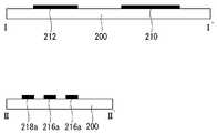
다음으로, 도 10 및 도 11을 참조하여 본 발명의 제 2 실시예에 따른 정정용량 방식 터치 스크린 패널에 대해 설명하기로 한다. 도 10은 본 발명의 제 2 실시예에 따른 터치 스크린 패널의 평면도, 도 11은 도 10에 도시된 본 발명의 제 2 실시예에 따른 터치 스크린 패널의 III-III'선 및 IV-IV'선을 따라 취한 단면도이다.Next, the capacitive touch screen panel according to the second embodiment of the present invention will be described with reference to FIGS. 10 and 11. 10 is a plan view of a touch screen panel according to a second embodiment of the present invention, and FIG. 11 is a line III-III 'and IV-IV' of a touch screen panel according to the second embodiment of the present invention shown in FIG. It is a cross-sectional view taken along.
도 10 및 도 11을 참조하면, 본 발명의 제 2 실시예에 따른 정전용량 방식 터치 스크린 패널은 전극형성부(A), 라우팅 배선부(B) 및 패드부(C)를 포함한다.10 and 11, the capacitive touch screen panel according to the second embodiment of the present invention includes an electrode forming unit A, a routing wiring unit B, and a pad unit C.
전극형성부(A)는 제 1 방향(예컨대, X축 방향)으로 나란하게 배열된 복수의 제 1 전극열들(230)과 상기 제 1 전극열들(230)과 교차하는 제 2 방향(예컨대, Y축 방향)으로 배열되는 복수의 제 2 전극열들(235)을 포함한다. 제 1 전극열들(230)의 각각은 삼각형, 사각형, 마름모꼴, 다각형 등으로 형성된 제 1 전극패턴들(231)과 이들 제 1 전극패턴들(231)을 연결하는 제 1 연결패턴들(210)을 포함한다. 제 2 전극열들(235)의 각각 또한 제 1 전극패턴들(231)과 유사한 삼각형, 사각형, 마름모꼴, 다각형 등으로 형성된 제 2 전극패턴들(236)과 이들 제 2 전극패턴들(236)을 서로 연결하는 제 2 연결패턴들(237)을 포함한다.The electrode forming unit A may have a plurality of
본 발명의 제 2 실시예에 따른 터치 스크린 패널에서, 제 1 연결패턴들(210)은 제 1 전극패턴들(231)과 별도로 형성되며, 제 2 연결패턴들(237)은 제 2 전극패턴들(236)과 일체로 형성된다.In the touch screen panel according to the second embodiment of the present invention, the
라우팅 배선부(B)는 전극형성부(A)의 외곽부에 형성되며 복수의 제 1 전극열들(230)과 각각 연결되는 복수의 제 1 라우팅 배선들(212)과 복수의 제 2 전극열들(235)과 각각 연결되는 복수의 제 2 라우팅 배선들(214)로 이루어 진다.The routing wire part B is formed at an outer portion of the electrode forming part A, and the plurality of
패드부(C)는 복수의 제 1 라우팅 배선들(212)을 통해 복수의 제 1 전극열들(230)과 각각 접속되는 복수의 제 1 패드들(216)과 복수의 제 2 라우팅 배선들(214)을 통해 복수의 제 2 전극열들(235)과 각각 접속되는 복수의 제 2 패드들(218)로 이루어 진다.The pad part C may include a plurality of
한편, 본 발명의 제 2 실시예에 따른 터치 스크린 패널에서는 제 1 연결패턴들(210)과 제 1 및 제 2 라우팅 배선들(212, 214)은 동일 공정을 통해 기판(200) 상에 형성되며, 동일물질을 이용하여 형성된다. 그러나, 본 발명이 이에 한정되는 것은 아니며, 제 1 연결패턴들(210)과 제 1 및 제 2 라우팅 배선들(212, 214)은 상이한 물질로 형성될 수도 있다. 제 1 연결패턴들(210)과 제 1 및 제 2 라우팅 배선들(212, 214)을 형성하는 재료로는 Al, AlNd, Mo, MoTi, Cu, Cr 등이 이용된다. 이들 재료는 비저항이 낮은 물질이기 때문에 전극 연결부위의 저항을 낮추는 효과가 있다. ITO(Indium Tin Oxide)는 비저항이 높기 때문에 두께를 두껍게 해야 하는 문제점이 있기는 하지만 비저항이 낮은 금속과 적층하여 사용될 수도 있다. 또한, 제 1 연결패턴들(210)은 2000Å~3000Å의 두께를 가지며, 3㎛~10㎛의 폭을 가지도록 형성하는 것이 바람직하다. 제 1 연결패턴들(210)의 두께가 2000Å미만일 경우에는 저항이 높아지고, 3000Å이상일 때에는 패턴의 단차가 심해지는 문제가 있으며, 제 1 연결패턴들(210)의 폭이 3㎛미만일 때에는 저항이 높아지고, 10㎛보다 클 경우에는 패턴이 시인되는 문제점이 있기 때문이다.Meanwhile, in the touch screen panel according to the second embodiment of the present invention, the
또한, 본 발명의 제 2 실시예에 따른 터치 스크린 패널의 제 1 연결패턴들(210)과 제 1 및 제 2 라우팅 배선들(212, 214)은 동일 공정을 통해 형성되기 때문에 전극패턴들을 연결하는 연결패턴과 라우팅 배선을 서로 상이한 공정에서 형성하는 종래기술에 비해 하나의 마스크 공정을 생략할 수 있어 비용절감 및 택트타임을 줄일 수 있는 효과도 얻을 수 있다.In addition, since the
본 발명의 제 2 실시예에 따른 터치 스크린 패널의 전극 형성부(A)에서는 제 1 연결패턴(210)의 제 1 부분(210a) 및 제 2 부분(210b)이 노출되도록 제 1 연결패턴(210) 상에 형성되며, 교차하는 제 1 연결패턴(210)과 제 2 연결패턴(237)이 서로 접촉되지 않도록 하는 제 1 절연패턴(220a)이 형성된다. 제 1 전극패턴들(231)은 기판(200) 상에 형성되나, 제 1 전극패턴(231)의 제 1 부분(231a)은 제 1 연결패턴(210)의 제 1 부분(210a) 상에, 제 1 전극패턴(231)의 제 2 부분(231b)은 제 1 연결패턴(210)의 제 2 부분(210b) 상에 각각 형성된다. 따라서, 서로 인접하는 제 1 전극패턴들(231)은 제 1 연결패턴(210)에 의해 전기적으로 접속된다. 도 11에서는 제 1 전극패턴(231)의 제 1 부분(231a) 및 제 2 부분(231b)이 제 1 연결패턴(210)의 제 1 및 제 2 부분의 측면 및 상면, 절연패턴(220)의 측면 및 상면 일부 상에 각각 형성되는 것으로 도시되어 있으나, 제 1 전극패턴(231)의 제 1 부분(231a) 및 제 2 부분(231b)은 제 1 연결패턴(210)의 제 1 및 제 2 부분의 측면 및 상면 또는 제 1 연결패턴(210)의 제 1 및 제 2 부분의 측면 및 상면과 절연패턴(220)의 측면의 일부 상에만 형성될 수도 있다.In the electrode forming portion A of the touch screen panel according to the second embodiment of the present invention, the
또한, 라우팅 배선부(B)에서는 전극 형성부(A)를 향한 제 1 라우팅 배선(212)의 일부(212a)와 제 2 라우팅 배선(214)의 일부(도시생략)가 노출되도록 제 2 절연패턴(220b)이 형성된다. 전극 형성부(A)의 최외측에 있는 제 1 전극패턴(231)의 제 2 부분(231b)은 제 1 라우팅 배선(212)의 측면 및 상면과 절연패턴(220)의 측면 및 상면 일부 상에 형성된다. 전극 형성부(A)의 최외측에 있는 제 2 전극패턴(236) 또한 그 일부가 제 1 전극패턴(231)과 유사하게 제 2 라우팅 배선(214)의 측면 및 상면과 절연패턴(220)의 측면 및 상면 일부 상에 형성된다. 그러나, 전극 형성부(A)의 최외측에 있는 제 2 전극패턴(236)은 그 일부가 제 2 라우팅 배선(214)의 측면 및 상면, 또는 제 2 라우팅 배선(214)의 일부(212a)의 측면 및 상면과 절연패턴(220)의 측면의 일부 상에만 형성될 수도 있다.In addition, in the routing wiring part B, a second insulating pattern such that a
또한, 패드부(C)에서는 도 11에 도시된 바와 같이 제 1 패드들(216) 및 제 2 패드들(218) 상에는 외부회로와의 접속을 위해 절연패턴이 형성되지 않으나, 제 1 패드들(216) 및 제 2 패드들(218) 상에 절연패턴을 형성하고, 각 패드들(216, 218)의 일부를 노출시키는 콘택홀을 절연패턴에 형성하면 제 1 패드들(216) 및 제 2 패드들(218) 상에 절연패턴을 형성하는 구성도 가능하다.In addition, in the pad part C, as shown in FIG. 11, an insulating pattern is not formed on the
제 1 및 제 2 절연패턴(220a, 220b)의 재료로는 질화실리콘(SiNx)이 이용된다. 제 1 절연패턴(220a)의 두께는 5,000Å 미만의 경우에는 제 1 전극열(230)과 제 2 전극열(235)에 걸리는 전압에 의해 제 1 절연패턴(220a)이 파괴되거나 손상될 수 있다. 따라서, 터치 스크린 패널의 사용중에 제 1 절연패턴(220a)이 파괴되거나 손상되어 고장이 발생하는 현상을 방지하기 위해서는 제 1 절연패턴(220a)의 두께를 5,000Å 이상으로 하는 것이 바람직하다. 또한, 제 1 절연패턴(220a)의 두께가 6,000Å 부근에서는 투과율이 더 이상 증가하지 않는 포화상태를 나타내고 색전이 현상 또한 최소로 된다. 즉, 투과율과 색도표현의 측면에서는 제 1 절연패턴(220a)의 두께가 6,000Å 이상일 때 투과율이 최대로 되고 색전이 현상도 최소로 되기 때문에 가장 바람직하다. 그러나, 절연층의 두께가 7,000Å를 초과하면 절연층의 재료로 이용되는 질화실리콘막의 특성상 전극 형성부(A)의 불필요한 부분에서 제거하는데 공정시간이 많이 소요되므로 바람직하지 못하다. 따라서, 절연층의 안정성과 양호한 광투과율 및 색도표현 능력을 종합해 보았을 때 절연층(220a)의 두께를 5,000Å~7,000Å의 범위로 하는 것이 바람직하다.Silicon nitride (SiNx) is used as the material of the first and second
제 1 및 제 2 전극패턴들(231, 236)과 제 2 연결패턴들(237)은 동일 공정을 통해 동일 재료로 형성된다. 제 1 및 제 2 전극패턴들(231, 236)과 제 2 연결패턴들(237)의 재료로는 ITO 또는 IZO의 투명도전물질이 이용된다. 터치 스크린 패널의 최상위층에 형성되는 제 1 및 제 2 전극패턴(231, 236)과 제 2 연결패턴들(237)을 ITO로 형성하면, ITO의 경도가 높기 때문에 터치 스크린 패널의 기판(200)의 다른 면에 표시장치를 형성하기 위한 후속 공정에서 스크래치가 발생하지 않게 되어 양호한 품질의 터치 스크린 패널이 얻어진다.The first and
이하, 도 12a 내지 도 14b를 참조하여, 본 발명의 제 2 실시예에 따른 정전용량 방식 터치 스크린 패널의 제조방법에 대해 설명하기로 한다.Hereinafter, a method of manufacturing a capacitive touch screen panel according to a second embodiment of the present invention will be described with reference to FIGS. 12A to 14B.
도 12a 및 도 12b는 본 발명의 제 2 실시예에 따르는 정전용량 방식 터치 스크린 패널의 제조방법 중 제 1 마스크 공정을 설명하기 위한 평면도 및 단면도이다.12A and 12B are plan and cross-sectional views illustrating a first mask process in the method of manufacturing the capacitive touch screen panel according to the second embodiment of the present invention.
도 10, 도 12a 및 도 12b를 참조하면, 제 1 마스크 공정을 이용하여 전극형성부(A), 라우팅 배선부(B) 및 패드부(C)를 구비하는 기판(200) 상에 제 1 연결패턴(210), 제 1 라우팅 배선(212) 및 제 2 라우팅 배선(214), 제 1 패드들의 하부층(216a) 및 제 2 패드들의 하부층(218a)을 포함하는 제 1 도전성 패턴군이 형성된다.10, 12A, and 12B, a first connection is performed on a
이를 보다 상세히 설명하면, 기판(200) 상에 스퍼터링 등의 증착공정을 통해 제 1 도전층이 전면증착된다. 그리고, 제 1 마스크를 이용한 포토리소그래피 공정과 식각공정으로 제 1 도전층이 패터닝됨으로써 제 1 연결패턴들(210), 제 1 라우팅 배선들(212), 제 2 라우팅 배선들(214), 제 1 패드들의 하부층(216a) 및 제 2 패드들의 하부층(218a)을 포함하는 제 1 도전성 패턴군이 형성된다. 여기에서 제 1 도전성 패턴군을 형성하는 재료로는 Al, AlNd, Mo, MoTi, Cu, Cr, 등이 이용된다. 제 1 도전성 패턴군 중 전극형성부(A, 도 10 참조)에 형성되는 제 1 연결패턴(210)의 두께는 2000Å~3000Å의 범위로, 폭은 3㎛~10㎛의 범위를 갖도록 형성된다.In more detail, the first conductive layer is entirely deposited on the
한편, 제 1 연결패턴(210), 제 1 라우팅 배선(212), 제 2 라우팅 배선(214), 제 1 패드들의 하부층(216a) 및 제 2 패드들의 하부층(218a)을 포함하는 제 1 도전성 패턴군은 기판(200) 상에 프린팅 방법으로 형성한 후, 건조 및 가열하여 형성할 수도 있다. 이 경우, 제 1 마스크 공정을 이용한 포토리소그래피 공정 및 에칭공정을 생략할 수 있게 된다. 제 1 도전성 패턴군은 인쇄법 외의 다른 패턴형성 방법을 이용하여 형성할 수도 있다.Meanwhile, a first conductive pattern including a
도 13a 및 도 13d는 본 발명의 제 2 실시예에 따르는 정전용량 방식 터치 스크린 패널의 제조방법 중 제 2 마스크 공정을 설명하기 위한 평면도 및 단면도이다. 도 13a에서 점선으로 표시된 제 1 및 제 2 라우팅 배선들(212, 214)은 제 2 절연패턴(220b)으로 덮여 있기 때문에 실질적으로는 평면도 상에서는 보이지 않는 부분이지만, 본 발명에서는 이해를 돕기 위해 점선으로 표시하였다.13A and 13D are plan views and cross-sectional views illustrating a second mask process in the method of manufacturing the capacitive touch screen panel according to the second embodiment of the present invention. The first and
도 13a 및 도 13b를 참조하면, 제 1 연결패턴(210), 제 1 라우팅 배선(212), 제 2 라우팅 배선(214), 제 1 패드의 하부층(216a) 및 제 2 패드의 하부층(218a) 을 포함하는 제 1 도전성 패턴군이 형성된 기판(200) 상의 전면에 스퍼터링 등의 증착방법을 통해 절연층(220)이 형성된다. 절연층(220)의 재료로는 질화 실리콘(SiNx) 등의 무기 절연물질이 이용된다. 절연층(220)의 두께는 바람직하게는 5,000Å~10,000Å의 범위로, 더욱 바람직하게는 5,000Å~7,000Å의 범위로 설정한다.13A and 13B, the
절연층(220)이 형성된 후, 도 13c에 도시된 바와 같이 제 2 마스크를 이용한 포토리소그래피 공정을 이용하여, 절연층(220)이 존재해야 하는 부분에 포토레지스트 패턴(1100)이 형성된다. 그리고, 포토레지스트 패턴(1100)을 이용한 건식 식각공정으로 전극 형성부(A)에서는 도 13d에 도시된 바와 같이, 제 1 연결패턴(210)의 제 1 부분(210a) 및 제 2 부분(210b)이 노출되도록 제 1 연결패턴(210) 상에 제 1 절연패턴(220a)이 형성되고, 라우팅부(B)에서는 제 1 라우팅 배선(212) 및 제 2 라우팅 배선(214)의 일부가 노출되도록 제 1 및 제 2 라우팅 배선 상에 제 2 절연패턴(220b)이 형성되며, 패드부(C)에서는 제 1 및 제 2 패드의 하부층들(216a, 218a)이 노출된다.After the insulating
도 14a 및 도 14b는 본 발명의 제 2 실시예에 따르는 정전용량 방식 터치 스크린 패널의 제조방법 중 제 3 마스크 공정을 설명하기 위한 평면도 및 단면도이다. 도 14a는 본 발명의 제 2 실시예에 따르는 정전용량 방식 터치 스크린 패널의 제조방법 중 제 3 마스크 공정에 의해 형성된 평면도를 도시한 도면으로서, 이해를 돕기 위해 라우팅 배선부(B)에 형성된 제 2 절연패턴(220b)을 생략한 도면이다.14A and 14B are plan views and cross-sectional views illustrating a third mask process in the method of manufacturing the capacitive touch screen panel according to the second embodiment of the present invention. FIG. 14A illustrates a plan view formed by a third mask process in a method of manufacturing a capacitive touch screen panel according to a second embodiment of the present invention. FIG. Insulating
도 14a 및 도 14b를 참조하면, 제 3 마스크 공정을 이용하여 제 1 연결패턴(210) 및 제 1 절연패턴(220a)이 형성된 기판(200) 상의 전극 형성부(A)에 제 1 방향(예를 들면, x 방향)으로 평행하게 배열되는 복수의 제 1 전극패턴들(231)과, 제 1 방향과 교차하는 제 2 방향(예를 들면, y 방향)으로 평행하게 배열되는 복수의 제 2 전극열들(235)을 포함하는 제 2 도전성 패턴군들이 형성된다.Referring to FIGS. 14A and 14B, the first direction (eg, in the electrode forming portion A on the
이를 보다 상세히 설명하면, 제 1 연결패턴(210) 및 제 1 절연패턴(220a)이 형성된 기판(200) 상의 전극 형성부(A)와 패드부(C) 상에 스퍼터링 등의 증착공정을 통해 제 2 도전층이 전면 증착된다. 그리고, 제 3 마스크를 이용한 포토리소그래피 공정과 식각공정으로 제 2 도전층이 패터닝됨으로써 제 1 방향(예를 들면, x 방향)으로 평행하게 배열되는 복수의 제 1 전극패턴들(231)과, 제 1 방향과 교차하는 제 2 방향(예를 들면, y 방향)으로 평행하게 배열되는 복수의 제 2 전극열들(235), 제 1 패드의 상부층(216b) 및 제 2 패드의 상부층(218b)을 포함하는 제 2 도전성 패턴군이 형성된다. 여기에서, 제 2 전극열들(235)의 각각은 복수의 제 2 전극패턴들(236)과 서로 이웃하는 제 2 전극패턴들(236)을 연결하는 제 2 연결패턴들(237)을 포함한다. 제 2 도전층의 재료로서는 ITO 또는 IZO 등의 투명도전물질이 이용되며, 그 두께를 1,200Å~1,600Å으로 하면 투과율을 최대로 하는 효과를 얻을 수 있다.In more detail, the electrode forming portion A and the pad portion C on the
제 3 마스크 공정의 결과로서, 터치 스크린 패널의 전극 형성부(A)에서는 제 1 전극패턴(231)의 제 1 부분(231a)이 제 1 연결패턴(210)의 제 1 부분(210a) 상에, 제 1 전극패턴(231)의 제 2 부분(231b)은 제 1 연결패턴(210)의 제 2 부분(210b) 상에 각각 형성되며, 제 1 전극패턴(231)의 제 1 부분(231a)과 제 2 부분(231b) 사이의 중간부(231c)는 기판(200) 상에 형성된다. 따라서, 서로 인접하는 제 1 전극패턴들(231)은 제 1 연결패턴(210)에 의해 전기적으로 접속된다. 도 14b에서는 제 1 전극패턴(231)의 제 1 부분(231a) 및 제 2 부분(231b)이 제 1 연결패턴(210)의 제 1 및 제 2 부분의 측면 및 상면, 제 1 절연패턴(220a)의 측면 및 상면 일부 상에 각각 형성되는 것으로 도시되어 있으나, 제 1 전극패턴(231)의 제 1 부분(231a) 및 제 2 부분(231b)은 제 1 연결패턴(210)의 제 1 및 제 2 부분의 측면 및 상면 또는 제 1 연결패턴(210)의 제 1 및 제 2 부분의 측면 및 상면과 제 1 절연패턴(220a)의 측면의 일부 상에만 각각 형성될 수도 있다.As a result of the third mask process, in the electrode forming portion A of the touch screen panel, the
또한, 라우팅 배선부(B)에서는 제 1 라우팅 배선(212)의 일부(212a)와 제 2 라우팅 배선(214)의 일부(도시생략)가 노출되도록 제 2 절연패턴(220b)이 형성된다. 전극 형성부(A)의 최외측에 있는 제 1 전극패턴(231)의 제 2 부분(231b)은 제 1 라우팅 배선(212)의 측면 및 상면과 제 2 절연패턴(220b)의 측면 및 상면 일부 상에 형성된다. 전극 형성부(A)의 최외측에 있는 제 2 전극패턴(236) 또한 그 일부가 제 1 전극패턴(231)과 유사하게 제 2 라우팅 배선(214)의 측면 및 상면과 제 2 절연패턴(220b)의 측면 및 상면 일부 상에 형성된다. 그러나, 전극 형성부(A)의 최외측에 있는 제 2 전극패턴(236)은 그 일부가 제 2 라우팅 배선(214)의 측면 및 상면, 또는 제 2 라우팅 배선(214)의 측면 및 상면과 제 2 절연패턴(220b)의 측면의 일부 상에만 형성될 수도 있다.In addition, in the routing wiring unit B, a second
또한, 패드부(C)에서는 상부층들(216b, 218b)이 하부층들(216a, 218a)을 각각 감싸도록 형성되는 제 1 패드(216) 및 제 2 패드(218)가 형성된다. 또한 패드부(C)는 도 14b에 도시된 바와 같이 제 1 패드들(216) 및 제 2 패드들(218) 상에는 외부회로와의 접속을 위해 절연패턴이 형성되지 않는 것으로 도시되어 있으나, 제 1 패드들(216) 및 제 2 패드들(218) 상에 절연패턴을 형성하고, 각 패드들(216, 218)의 일부를 노출시키는 콘택홀을 절연패턴에 형성하면 제 1 패드들(216) 및 제 2 패드들(218) 상에 절연패턴을 형성하는 구성도 가능하다.In addition, in the pad part C, the
다음으로, 도 15 및 도 16을 참조하여 본 발명의 제 3 실시예에 따른 액정표시장치용 어레이 기판에 대해 설명하기로 한다. 도 15는 본 발명의 제 3 실시예에 따른 터치 스크린 패널의 평면도, 도 16은 도 15에 도시된 본 발명의 제 3 실시예에 따른 터치 스크린 패널의 V-V'선 및 VI-VI'선을 따라 취한 단면도이다.Next, an array substrate for a liquid crystal display device according to a third embodiment of the present invention will be described with reference to FIGS. 15 and 16. 15 is a plan view of a touch screen panel according to a third embodiment of the present invention, and FIG. 16 is a V-V 'line and a VI-VI' line of the touch screen panel according to the third embodiment of the present invention shown in FIG. It is a cross-sectional view taken along.
도 15 및 도 16을 참조하면, 본 발명의 제 3 실시예에 따른 정전용량 방식 터치 스크린 패널은 전극형성부(A), 라우팅 배선부(B) 및 패드부(C)를 포함한다.15 and 16, the capacitive touch screen panel according to the third embodiment of the present invention includes an electrode forming unit A, a routing wiring unit B, and a pad unit C.
전극형성부(A)는 제 1 방향(예컨대, X축 방향)으로 나란하게 배열된 복수의 제 1 전극열들(330)과 상기 제 1 전극열들(330)과 교차하는 제 2 방향(예컨대, Y축 방향)으로 배열되는 복수의 제 2 전극열들(335)을 포함한다. 제 1 전극열들(330)의 각각은 삼각형, 사각형, 마름모꼴, 다각형 등으로 형성된 제 1 전극패턴들(331)과 이들 제 1 전극패턴들(331)을 연결하는 제 1 연결패턴들(310)을 포함한다. 제 2 전극열들(335)의 각각 또한 제 1 전극패턴들(331)과 유사한 삼각형, 사각형, 마름모꼴, 다각형 등으로 형성된 제 2 전극패턴들(336)과 이들 제 2 전극패턴들(336)을 서로 연결하는 제 2 연결패턴들(337)을 포함한다.The electrode forming unit A may have a plurality of
본 발명의 제 3 실시예에 따른 터치 스크린 패널에서, 제 1 연결패턴들(310)은 제 1 전극패턴들(331)과 별도로 형성되며, 제 2 연결패턴들(337)은 제 2 전극패턴들(336)과 일체로 형성된다.In the touch screen panel according to the third embodiment of the present invention, the
라우팅 배선부(B)는 전극형성부(A)의 외곽부에 형성되며 복수의 제 1 전극열들(330)과 각각 연결되는 복수의 제 1 라우팅 배선들(312)과 복수의 제 2 전극열들(335)과 각각 연결되는 복수의 제 2 라우팅 배선들(314)로 이루어 진다.The routing wiring part B is formed at an outer portion of the electrode forming part A, and the plurality of
패드부(C)는 복수의 제 1 라우팅 배선들(312)을 통해 복수의 제 1 전극열들(330)과 각각 접속되는 복수의 제 1 패드들(316)과 복수의 제 2 라우팅 배선들(314)을 통해 복수의 제 2 전극열들(335)과 각각 접속되는 복수의 제 2 패드들(318)로 이루어 진다.The pad part C may include a plurality of
한편, 본 발명의 제 3 실시예에 따른 터치 스크린 패널에서는 제 1 및 제 2 실시예와는 달리 제 1 연결패턴들(310)과 제 1 및 제 2 라우팅 배선들(312, 314)은 상이한 물질로 형성된다. 제 1 및 제 2 라우팅 배선들(312, 314)은 단일 금속층 또는 복수의 금속층으로 형성될 수 있다. 제 1 및 제 2 라우팅 배선들(312, 314)이 복수의 금속층으로 형성될 경우 하부층(312a, 314a)은 Al, AlNd, Mo, MoTi, Cu, Cr 등으로 형성되고, 상부층(312b, 314b)는 ITO 또는 IZO 등으로 형성된다. 제 1 연결패턴들(310)은 ITO 또는 IZO 등의 투명도전물질로 형성된다. 또한, 제 1 연결패턴들(310)은 2000Å~3000Å의 두께를 가지며, 3㎛~10㎛의 폭을 가지도록 형성하는 것이 바람직하다. 제 1 연결패턴들(310)의 두께가 2000Å미만일 경우에는 저항이 높아지고, 3000Å이상일 때에는 패턴의 단차가 심해지는 문제가 있으며, 제 1 연결패턴들(210)의 폭이 3㎛미만일 때에는 저항이 높아지고, 10㎛보다 클 경우에는 패턴이 시인되는 문제점이 있기 때문이다.Meanwhile, in the touch screen panel according to the third embodiment of the present invention, unlike the first and second embodiments, the
또한, 본 발명의 제 3 실시예에 따른 터치 스크린 패널을 제조하기 위해 마스크 공정을 이용할 경우 제 1 연결패턴들(310)과 제 1 및 제 2 라우팅 배선들(312, 314)이 상이한 공정을 통해 형성되기 때문에 4마스크 공정이 사용된다.In addition, when the mask process is used to manufacture the touch screen panel according to the third embodiment of the present invention, the
본 발명의 제 3 실시예에 따른 터치 스크린 패널의 전극 형성부(A)에서는 제 1 연결패턴(310)의 제 1 부분(310a) 및 제 2 부분(310b)이 노출되도록 제 1 연결패턴(310) 상에 형성되며, 상호 교차하는 제 1 연결패턴(310)과 제 2 연결패턴(337)이 서로 접촉되지 않도록 하는 제 1 절연패턴(320a)이 형성된다. 제 1 전극패턴들(331)은 기판(300) 상에 형성되나, 제 1 전극패턴(331)의 제 1 부분(331a)은 제 1 연결패턴(310)의 제 1 부분(310a) 상에, 제 1 전극패턴(331)의 제 2 부분(331b)은 제 1 연결패턴(310)의 제 2 부분(310b) 상에 각각 형성된다. 따라서, 서로 인접하는 제 1 전극패턴들(331)은 제 1 연결패턴(310)에 의해 전기적으로 접속된다. 도 16에서는 제 1 전극패턴(331)의 제 1 부분(331a) 및 제 2 부분(331b)이 제 1 연결패턴(310)의 제 1 및 제 2 부분의 측면 및 상면, 제 1 절연패턴(320a)의 측면 및 상면 일부 상에 각각 형성되는 것으로 도시되어 있으나, 제 1 전극패턴(331)의 제 1 부분(331a) 및 제 2 부분(331b)은 제 1 연결패턴(310)의 제 1 및 제 2 부분의 측면 및 상면 및 상면 또는 제 1 연결패턴(310)의 제 1 및 제 2 부분의 측면 및 상면과 제 1 절연패턴(320a)의 측면의 적어도 일부 상에 형성될 수도 있다.In the electrode forming portion A of the touch screen panel according to the third embodiment of the present invention, the
또한, 라우팅 배선부(B)에서는 전극 형성부(A)를 향한 제 1 라우팅 배선(312)의 일부(312a)와 제 2 라우팅 배선(314)의 일부(도시생략)가 노출되도록 제 1 절연패턴(320a)이 형성된다. 전극 형성부(A)의 최외측에 있는 제 1 전극패턴(331)의 제 2 부분(331b)은 제 1 라우팅 배선(312)의 측면 및 상면과 절연패턴(320)의 측면 및 상면의 일부 상에 형성된다. 전극 형성부(A)의 최외측에 있는 제 2 전극패턴(336) 또한 그 일부가 제 1 전극패턴(331)과 유사하게 제 2 라우팅 배선(314)의 측면 및 상면과 절연패턴(320)의 측면 및 상면 일부 상에 형성된다. 그러나, 전극 형성부(A)의 최외측에 있는 제 2 전극패턴(336)은 그 일부가 제 2 라우팅 배선(314)의 측면 및 상면, 또는 제 2 라우팅 배선(314)의 측면 및 상면과 절연패턴(320)의 측면의 적어도 일부 상에 형성될 수도 있다.In addition, in the routing wiring part B, the first insulating pattern such that a
또한, 패드부(C)에서는 도 16에 도시된 바와 같이 제 1 패드들(316) 및 제 2 패드들(318) 상에는 외부회로와의 접속을 위해 절연패턴이 형성되지 않으나, 제 1 패드들(316) 및 제 2 패드들(318) 상에 절연패턴을 형성하고, 각 패드들(316, 318)의 일부를 노출시키는 콘택홀을 절연패턴에 형성하면 제 1 패드들(316) 및 제 2 패드들(318) 상에 절연패턴을 형성하는 구성도 가능하다.In addition, in the pad part C, as illustrated in FIG. 16, an insulating pattern is not formed on the
제 1 및 제 2 절연패턴(320a, 320b)의 재료로는 질화실리콘(SiNx)이 이용된다. 제 1 절연패턴(320a)의 두께는 5,000Å 미만의 경우에는 제 1 전극열(330)과 제 2 전극열(335)에 걸리는 전압에 의해 제 1 절연패턴(320a)이 파괴되거나 손상될 수 있다. 따라서, 터치 스크린 패널의 사용중에 제 1 절연패턴(320a)이 파괴되거나 손상되어 고장이 발생하는 현상을 방지하기 위해서는 제 1 절연패턴(320a)의 두께를 5,000Å 이상으로 하는 것이 바람직하다. 또한, 제 1 절연패턴(320a)의 두께가 6,000Å 부근에서는 투과율이 더 이상 증가하지 않는 포화상태를 나타내고 색전이 현상 또한 최소로 된다. 즉, 투과율과 색도표현의 측면에서는 제 1 절연패턴(320a)의 두께가 6,000Å 이상일 때 투과율이 최대로 되고 색전이 현상도 최소로 되기 때문에 가장 바람직하다. 그러나, 제 1 절연패턴(320a)의 두께가 7,000Å를 초과하면 제 1 절연패턴(320a)의 재료로 이용되는 질화실리콘막의 특성상 전극 형성부(A)의 불필요한 부분에서 제거하는데 공정시간이 많이 소요되므로 바람직하지 못하다. 따라서, 제 1 절연패턴(320a)의 안정성과 양호한 광투과율 및 색도표현 능력을 종합해 보았을 때 제 1 절연패턴(320a)의 두께를 5,000Å~7,000Å의 범위로 하는 것이 바람직하다.Silicon nitride (SiNx) is used as a material of the first and second
본 발명의 제 3 실시예에 따르는 터치 스크린 패널에서는 제 1 및 제 2 전극패턴들(331, 336)과 제 2 연결패턴들(337)의 재료로서 ITO 또는 IZO의 투명도전물질이 이용된다. 터치 스크린 패널의 최상위층에 ITO를 이용한 제 1 및 제 2 전극패턴(331, 336)과 제 2 연결패턴들(337)을 형성하면, ITO의 경도가 높기 때문에 터치 스크린 패널의 기판(300)의 다른 면에 표시장치를 형성하기 위한 후속 공정에서 스크래치가 발생하지 않게 되어 양호한 품질의 터치 스크린 패널이 얻어진다.In the touch screen panel according to the third embodiment of the present invention, a transparent conductive material of ITO or IZO is used as a material of the first and
이하, 도 17a 내지 도 20b를 참조하여, 본 발명의 제 3 실시예에 따른 정전용량 방식 터치 스크린 패널의 제조방법에 대해 설명하기로 한다.Hereinafter, a method of manufacturing a capacitive touch screen panel according to a third embodiment of the present invention will be described with reference to FIGS. 17A to 20B.
도 17a 및 도 17b는 본 발명의 제 3 실시예에 따르는 정전용량 방식 터치 스크린 패널의 제조방법 중 제 1 마스크 공정을 설명하기 위한 평면도 및 단면도이다.17A and 17B are plan and cross-sectional views illustrating a first mask process in the method of manufacturing the capacitive touch screen panel according to the third embodiment of the present invention.
도 15, 도 17a 및 도 17b를 참조하면, 제 1 마스크 공정을 이용하여 전극형성부(A), 라우팅 배선부(B) 및 패드부(C)를 구비하는 기판(300) 상에 제 1 라우팅 배선의 하부층(312a), 제 2 라우팅 배선의 하부층(314a), 제 1 패드의 하부층(316a) 및 제 2 패드의 하부층(318a)을 포함하는 제 1 도전성 패턴군이 형성된다.15, 17A, and 17B, a first routing is performed on a
이를 보다 상세히 설명하면, 기판(300) 상에 스퍼터링 등의 증착공정을 통해 제 1 도전층이 전면증착된다. 그리고, 제 1 마스크를 이용한 포토리소그래피 공정과 식각공정으로 제 1 도전층이 패터닝됨으로써 제 1 라우팅 배선들(312) 및 제 2 라우팅 배선들(314), 제 1 패드들의 하부층(316a) 및 제 2 패드들의 하부층(318a)을 포함하는 제 1 도전성 패턴군이 형성된다. 여기에서 제 1 도전성 패턴군을 형성하는 재료로는 Al, AlNd, Mo, MoTi, Cu, Cr 등이 이용된다.In more detail, the first conductive layer is entirely deposited on the
한편, 제 1 라우팅 배선의 하부층(312a), 제 2 라우팅 배선의 하부층(314), 제 1 패드의 하부층(316a) 및 제 2 패드의 하부층(318a)을 포함하는 제 1 도전성 패턴군은 기판(300) 상에 프린팅 방법으로 형성한 후, 건조 및 가열하여 형성할 수도 있다. 이 경우, 제 1 마스크 공정을 이용한 포토리소그래피 공정 및 에칭공정을 생략할 수 있게 된다. 제 1 도전성 패턴군은 인쇄법 외의 다른 패턴형성 방법을 이용하여 형성할 수도 있다.Meanwhile, the first conductive pattern group including the
다음으로 제 1 및 제 2 라우팅 배선의 하부층들(312a, 314a)이 형성된 기판(300) 상에 스퍼터링 등의 증착공정을 통해 제 2 도전층이 전면증착된다. 그리고, 제 2 마스크를 이용한 포토리소그래피 공정과 식각공정으로 제 2 도전층을 패터닝함으로써 전극 형성부(A)의 기판(300)상에는 평행하게 배열된 복수의 제 1 연결패턴들(310)이 형성되고, 라우팅 배선부(B)의 하부층들(312a, 314a) 상에는 각각 제 1 라우팅 배선들의 상부층(312b) 및 제 2 라우팅 배선들의 상부층(도시생략)이 형성되며, 패드부(C)의 하부층들(316a 318a) 상에는 제 1 패드들의 상부층들(316b) 및 제 2 패드들의 상부층들(318b))이 각각 형성된다. 제 1 연결패턴(310)의 두께는 2000Å~3000Å의 범위로, 폭은 3㎛~10㎛의 범위를 갖도록 형성된다.Next, the second conductive layer is entirely deposited on the
도 19a 및 도 19d는 본 발명의 제 3 실시예에 따르는 정전용량 방식 터치 스크린 패널의 제조방법 중 제 3 마스크 공정을 설명하기 위한 평면도 및 단면도이다. 도 19a에서 점선으로 표시된 제 1 및 제 2 라우팅 배선들(312, 314)은 제 2 절연패턴(320b)으로 덮여 있기 때문에 실질적으로는 평면도 상에서는 보이지 않는 부분이지만, 본 발명에서는 이해를 돕기 위해 점선으로 표시하였다.19A and 19D are plan views and cross-sectional views illustrating a third mask process in the method of manufacturing the capacitive touch screen panel according to the third embodiment of the present invention. The first and
도 19a 및 도 19b를 참조하면, 제 1 연결패턴(310), 제 1 라우팅 배선(312) 및 제 2 라우팅 배선(314), 제 1 패드(316) 및 제 2 패드(318)를 포함하는 도전성 패턴군이 형성된 기판(300) 상의 전면에 스퍼터링 등의 증착방법을 통해 절연층(320)이 형성된다. 절연층(320)의 재료로는 질화 실리콘(SiNx) 등의 무기 절연물질이 이용된다. 절연층(320)의 두께는 바람직하게는 5,000Å~10,000Å의 범위로, 더욱 바람직하게는 5,000Å~7,000Å의 범위로 설정한다.Referring to FIGS. 19A and 19B, the conductive layer may include a
절연층(320)이 형성된 후, 도 19c에 도시된 바와 같이 제 3 마스크를 이용한 포토리소그래피 공정을 이용하여, 절연층(320)이 존재해야 하는 부분에 포토레지스트 패턴(1200)이 형성된다. 그리고, 포토레지스트 패턴(1200)을 이용한 건식 식각공정으로 전극 형성부(A)에서는 도 19d에 도시된 바와 같이 제 1 연결패턴(310)의 제 1 부분(310a) 및 제 2 부분(310b)이 노출되도록 제 1 연결패턴(310) 상에 제 1 절연패턴(320a)이 형성되고, 라우팅부(B)에서는 제 1 라우팅 배선(312) 및 제 2 라우팅 배선(314)의 일부가 노출되도록 제 1 및 제 2 라우팅 배선 상에 제 2 절연패턴(220b)이 형성되며, 패드부(C)에서는 제 1 및 제 2 패드의 하부층들(316a, 318a)이 노출된다.After the insulating
도 20a 및 도 20b는 본 발명의 제 3 실시예에 따르는 정전용량 방식 터치 스크린 패널의 제조방법 중 제 4 마스크 공정을 설명하기 위한 평면도 및 단면도이다. 도 20a는 본 발명의 제 3 실시예에 따르는 정전용량 방식 터치 스크린 패널의 제조방법 중 제 4 마스크 공정에 의해 형성된 평면도를 도시한 도면으로서, 이해를 돕기 위해 라우팅 배선부(B)에 형성된 제 2 절연패턴(320b)을 생략한 도면이다.20A and 20B are plan and cross-sectional views illustrating a fourth mask process in the method of manufacturing the capacitive touch screen panel according to the third embodiment of the present invention. FIG. 20A illustrates a plan view formed by a fourth mask process in a method of manufacturing a capacitive touch screen panel according to a third embodiment of the present invention.
도 20a 및 도 20b를 참조하면, 제 4 마스크 공정을 이용하여 제 1 연결패턴(310) 및 제 1 절연패턴(320a)이 형성된 기판(300) 상의 전극 형성부(A)에 제 1 방향(예를 들면, x 방향)으로 평행하게 배열되는 복수의 제 1 전극패턴들(331)과, 제 1 방향과 교차하는 제 2 방향(예를 들면, y 방향)으로 평행하게 배열되는 복수의 제 2 전극열들(335)을 포함하는 제 3 도전성 패턴군들이 형성된다.Referring to FIGS. 20A and 20B, the first direction (eg, in the electrode forming portion A on the
이를 보다 상세히 설명하면, 제 1 연결패턴(310) 및 제 1 절연패턴(320a)이 형성된 기판(300) 상의 전극 형성부(A)와 패드부(C) 상에 스퍼터링 등의 증착공정을 통해 제 3 도전층이 전면 증착된다. 그리고, 제 4 마스크를 이용한 포토리소그래피 공정과 식각공정으로 제 3 도전층이 패터닝됨으로써 제 1 방향(예를 들면, x 방향)으로 평행하게 배열되는 복수의 제 1 전극패턴들(331)과, 제 1 방향과 교차하는 제 2 방향(예를 들면, y 방향)으로 평행하게 배열되는 복수의 제 2 전극열들(335), 제1 패드의 상부층(316b) 및 제 2 패드의 상부층(318b)을 포함하는 제 3 도전성 패턴군이 형성된다. 여기에서, 제 2 전극열들(335)의 각각은 복수의 제 2 전극패턴들(336)과 서로 이웃하는 제 2 전극패턴들(336)을 연결하는 제 2 연결패턴들(337)을 포함한다. 제 3 도전층의 재료로서는 ITO 또는 IZO 등의 투명도전물질이 이용되며, 그 두께를 1,200Å~1,600Å으로 하면 투과율을 최대로 하는 효과를 얻을 수 있다.In more detail, the electrode forming part A and the pad part C on the
제 4 마스크 공정의 결과로서, 터치 스크린 패널의 전극 형성부(A)에서는 제 1 전극패턴(331)의 제 1 부분(331a)이 제 1 연결패턴(310)의 제 1 부분(310a) 상에, 제 1 전극패턴(331)의 제 2 부분(331b)이 제 1 연결패턴(310)의 제 2 부분(310b) 상에 각각 형성되며, 제 1 전극패턴(331)의 제 1 부분(331a)과 제 2 부분(331b) 사이의 중간부(331c)는 기판(300) 상에 형성된다. 따라서, 서로 인접하는 제 1 전극패턴들(331)은 제 1 연결패턴(310)에 의해 전기적으로 접속된다. 도 20b에서는 제 1 전극패턴(331)의 제 1 부분(331a) 및 제 2 부분(331b)이 제 1 연결패턴(310)의 제 1 및 제 2 부분의 측면 및 상면, 제 1 절연패턴(320a)의 측면 및 상면 일부 상에 각각 형성되는 것으로 도시되어 있으나, 제 1 전극패턴(331)의 제 1 부분(331a) 및 제 2 부분(331b)은 제 1 연결패턴(310)의 제 1 및 제 2 부분의 측면 및 상면 또는 제 1 연결패턴(310)의 제 1 및 제 2 부분의 측면 및 상면과 제 1 절연패턴(320a)의 측면의 일부 상에만 각각 형성될 수도 있다.As a result of the fourth mask process, in the electrode forming portion A of the touch screen panel, the
또한, 라우팅 배선부(B)에서는 제 1 라우팅 배선(312)의 일부와 제 2 라우팅 배선(314)의 일부가 노출되도록 제 2 절연패턴(320b)이 형성된다. 전극 형성부(A)의 최외측에 있는 제 1 전극패턴(331)의 제 2 부분(331b)은 제 1 라우팅 배선(312)의 측면 및 상면과 제 2 절연패턴(320b)의 측면 및 상면 일부 상에 형성된다. 전극 형성부(A)의 최외측에 있는 제 2 전극패턴(336) 또한 그 일부가 제 1 전극패턴(331)과 유사하게 제 2 라우팅 배선(314)의 측면 및 상면과 제 2 절연패턴(320b)의 측면 및 상면 일부 상에 형성된다. 그러나, 전극 형성부(A)의 최외측에 있는 제 2 전극패턴(336)은 그 일부가 제 2 라우팅 배선(314)의 측면 및 상면, 또는 제 2 라우팅 배선(314)의 측면 및 상면과 제 2 절연패턴(320b)의 측면의 일부 상에만 형성될 수도 있다.In addition, in the routing wiring part B, a second
또한, 패드부(C)에서는 상부층들(316b, 318b)이 하부층들(316a, 318a)을 각각 감싸도록 형성되는 제 1 패드(316) 및 제 2 패드(318)가 형성된다. 또한 패드부(C)에서는 도 20b에 도시된 바와 같이 제 1 패드들(316) 및 제 2 패드들(318) 상에는 외부회로와의 접속을 위해 절연패턴이 형성되지 않은 것으로 도시되어 있으나, 제 1 패드들(316) 및 제 2 패드들(318) 상에 절연패턴을 형성하고, 각 패드들(316, 318)의 일부를 노출시키는 콘택홀을 절연패턴에 형성하면 제 1 패드들(316) 및 제 2 패드들(318) 상에 절연패턴을 형성하는 구성도 가능하다.In addition, in the pad part C, the
이상 설명한 본 발명의 제 3 실시예에 따른 터치 스크린 패널에서는 제 1 연결패턴들(310)과 제 1 및 제 2 라우팅 배선들(312, 314)이 상이한 물질로 형성되는 경우의 예로서, 제 1 및 제 2 라우팅 배선들이 Al, AlNd, Mo, MoTi, Cu, 또는 Cr 등의 하부층(312a, 314a)과 ITO 또는 IZO 등의 상부층(312b, 314b)으로 형성되고, 제 1 연결패턴들이 ITO 또는 IZO 등의 투명도전물질로 형성되는 경우를 설명하였으나, 본 발명이 이에 한정되는 것은 아니다.In the touch screen panel according to the third embodiment of the present invention described above, the
예컨대, 도 20c에 도시된 바와 같이 제 1 라우팅 배선(312) 및 제 2 라우팅 배선들(도시생략)은 Al, AlNd, Mo, MoTi, Cu, 또는 Cr 등의 하부층(312a)과 ITO 또는 IZO 등의 상부층(312b)으로 형성되고, 제 1 연결패턴(311)은 제 1 및 제 2 라우팅 배선들과 마찬가지로 Al, AlNd, Mo, MoTi, Cu, 또는 Cr 등의 하부층(311a)과 ITO 또는 IZO 등의 상부층(311b)으로 형성될 수도 있다. 이와 같이 할 경우, 상기 제 1 라우팅 배선들(312) 및 제 2 라우팅 배선들(도시생략)과 제 1 연결패턴들(311)을 형성하기 위한 제 3 실시예의 제 1 마스크 공정 및 제 2 마스크 공정을 하나의 마스크 공정으로 수행할 수 있게 되므로 제 3 실시예보다 적어도 하나의 마스크 수를 절감할 수 있게 된다.For example, as illustrated in FIG. 20C, the
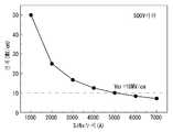
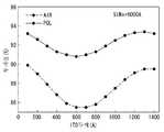
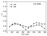
도 21 내지 도 23은 제 1 및 제 2 전극패턴들로서 ITO를 이용하고, 절연층으로서 실리콘 질화물을 이용하여 형성한 터치 스크린 패널에서 실리콘 질화물의 두께에 따른 항복전압, 투과율, 색전이의 특성을 시뮬레이션한 그래프들이다.21 to 23 illustrate characteristics of breakdown voltage, transmittance, and color transition according to the thickness of silicon nitride in a touch screen panel formed using ITO as the first and second electrode patterns and silicon nitride as the insulating layer. One graph.
도 21은 제 1 및 제 2 전극패턴들로 이용한 ITO의 두께를 1,400Å으로 형성하였을 경우, 절연층으로서 이용된 실리콘 질화물의 두께에 따라 절연층이 파괴되거나 손상되는 항복점의 전계값을 나타낸 그래프이다. 도 21에서 가로축은 실리콘 질화물의 두께(Å, 옹스트롬)를, 그리고 세로축은 전기장의 세기(MV/cm)를 각각 나타낸다. 도 21에 도시된 바와 같이, 실리콘 질화물은 10 메가볼트/cm 이상의 전계가 인가되면 파괴되거나 손상되므로 실리콘 질화물의 두께를 적절히 조정하는 것이 매우 중요하다. 터치 스크린 패널의 제 1 및 제 2 전극패턴들 사이에 500볼트 이하의 전압(이 값은 터치 스크린 패널 제조업체의 신뢰성 조건임)이 인가되는 조건에서, 실리콘 질화물의 두께가 5,000Å 이하에서는 실리콘 질화물의 절연이 파괴되거나 손상됨을 발견하였다. 따라서, 실리콘 질화물의 두께는 적어도 5,000Å 이상으로 형성하여야 한다.FIG. 21 is a graph showing an electric field value of a yield point at which an insulating layer is broken or damaged depending on the thickness of silicon nitride used as an insulating layer when the thickness of ITO used as the first and second electrode patterns is 1,400 μs. . In FIG. 21, the horizontal axis represents thickness of silicon nitride (Å, angstrom), and the vertical axis represents intensity of electric field (MV / cm), respectively. As shown in FIG. 21, silicon nitride is destroyed or damaged when an electric field of 10 megavolts / cm or more is applied, so it is very important to properly adjust the thickness of silicon nitride. Under the condition that a voltage of 500 volts or less (this value is a reliability condition of the touch screen panel manufacturer) is applied between the first and second electrode patterns of the touch screen panel, when the thickness of the silicon nitride is 5,000 Å or less, It has been found that the insulation is broken or damaged. Therefore, the silicon nitride should be formed at least 5,000 mm thick.
도 22는 제 1 및 제 2 전극패턴들로 이용한 ITO의 두께를 1,400Å으로 형성하였을 경우, 절연층으로서 이용된 실리콘 질화물의 두께에 따른 터치 스크린 패널의 투과율을 나타낸 그래프이다. 도 22에서, 가로축은 실리콘 질화물의 두께(Å, 옹스트롬)를, 세로축은 투과율(%)을 각각 나타내며, AIR는 터치 스크린 패널에 편광시트가 부착되지 않은 경우의 투과율을, POL은 터치 스크린 패널에 편광시트가 부착된 경우의 투과율을 각각 나타낸다. 도 22로부터 알 수 있는 바와 같이, 투과율은 절연층이 파괴거나 손상되지 않는 5000Å 이상을 기준으로 보면, 5000Å에서 점차 증가하다가 6000Å에서 피크치에 이르며 다시 6,500Å 까지 하락하고, 다시 7,000Å까지 증가하는 양상을 볼 수 있다. 즉, 절연층의 두께가 6,000Å 이상에서는 투과율이 포화되는 양상을 나타내기 때문에 두께 편차가 나더라도 큰 변화가 없다고 할 수 있다. 도 22로부터 터치 스크린 패널 단판으로는 89% 수준의 투과율을 보여주고, 편광시트를 부착하면 93% 수준의 투과율을 얻을 수 있음을 알 수 있다.FIG. 22 is a graph illustrating transmittance of a touch screen panel according to a thickness of silicon nitride used as an insulating layer when the thickness of ITO used as the first and second electrode patterns is 1,400 kPa. In FIG. 22, the horizontal axis represents thickness of silicon nitride (Å, angstrom), the vertical axis represents transmittance (%), respectively, AIR represents transmittance when a polarizing sheet is not attached to the touch screen panel, and POL represents a touch screen panel. The transmittance | permeability in the case where a polarizing sheet is affixed is shown, respectively. As can be seen from Fig. 22, the transmittance is increased from 5000 보면 to 5000 Å and then peaked at 6,000 하락 to 6,500 다시 again, and then increased to 7,000 보면 based on 5000 Å or more, where the insulating layer is not broken or damaged. Can be seen. That is, since the transmittance is saturated when the thickness of the insulating layer is 6,000 Pa or more, it can be said that there is no great change even if the thickness variation occurs. It can be seen from FIG. 22 that the transmittance of 89% is shown in the touch screen panel single plate, and the transmittance of 93% is obtained by attaching the polarizing sheet.
도 23은 제 1 및 제 2 전극패턴들로 이용한 ITO의 두께를 1,400Å으로 형성하였을 경우, 절연층으로서 이용된 실리콘 질화물의 두께에 따른 터치 스크린 패널의 색전이 특성을 나타낸 그래프이다. 도 23에서 가로축은 실리콘 질화물의 두께(Å, 옹스트롬)를, 세로축은 색차를 각각 나타내며, AIR는 터치 스크린 패널에 편광시트가 형성되지 않은 경우의 색차를, POL은 터치 스크린 패널에 편광시트가 형성된 경우의 색차를 각각 나타낸다. 도 23으로부터 알 수 있는 바와 같이, 투과율의 경우와 유사하게 절연층이 파괴되거나 손상되지 않는 5000Å 이상을 기준으로 보면, 색전이 특특성 또한 투과율 특성의 경우와 유사함을 알 수 있다.FIG. 23 is a graph illustrating color transition characteristics of a touch screen panel according to a thickness of silicon nitride used as an insulating layer when the thickness of ITO used as the first and second electrode patterns is 1,400 kPa. In FIG. 23, the horizontal axis represents thickness of silicon nitride (Å, angstrom) and the vertical axis represents color difference, respectively, AIR represents color difference when no polarizing sheet is formed on the touch screen panel, and POL forms polarizing sheet on the touch screen panel. The color difference of the case is shown, respectively. As can be seen from FIG. 23, similar to the case of transmittance, the embolic characteristic is also similar to that of the transmittance characteristic based on 5000 kPa or more, in which the insulating layer is not broken or damaged.
도 24 및 도 25는 제 1 및 제 2 전극패턴들로서 ITO를 이용하고, 절연층으로서 실리콘 질화물을 이용하여 형성한 터치 스크린 패널에서 ITO막의 두께에 따른 투과율 특성과 색전이 특성을 시뮬레이션한 그래프들이다.24 and 25 are graphs simulating transmittance characteristics and color transition characteristics according to the thickness of the ITO film in a touch screen panel formed using ITO as the first and second electrode patterns and silicon nitride as the insulating layer.
도 24는 절연층으로서 형성한 실리콘 질화물의 두께를 6,000Å으로 형성하였을 경우, 제 1 및 제 2 전극패턴들로 이용한 ITO의 두께에 따른 투과율의 특성을 도시한 그래프이다. 도 24에서, 가로축은 ITO막의 두께(Å, 옹스트롬)를, 세로축은 투과율(%)을 각각 나타내고, AIR는 터치 스크린 패널에 편광시트가 형성되지 않은 경우의 투과율을, POL은 터치 스크린 패널에 편광시트가 형성된 경우의 투과율을 각각 나타낸다. 도 24로부터 알 수 있는 바와 같이, 실리콘 질화물의 두께를 6,000Å에 고정하고 ITO두께에 따른 광투과율을 측정하면 700Å에서 최소가 되고 1400Å에서 최대가 됨을 확인할 수 있다.FIG. 24 is a graph showing the characteristics of transmittance according to the thickness of ITO used as the first and second electrode patterns when the thickness of the silicon nitride formed as the insulating layer is 6,000 kPa. In Figure 24, the horizontal axis represents the thickness of the ITO film (Å, Angstrom), the vertical axis represents the transmittance (%), respectively, AIR is the transmittance when no polarizing sheet is formed on the touch screen panel, POL is polarized on the touch screen panel The transmittance | permeability in the case where a sheet is formed is shown, respectively. As can be seen from FIG. 24, when the thickness of silicon nitride is fixed at 6,000 kW and the light transmittance according to the ITO thickness is measured, it can be confirmed that the minimum is 700 kW and the maximum is 1400 kW.
도 25는 절연층으로서 형성한 실리콘 질화물의 두께를 6,000Å으로 형성하였을 경우, 제 1 및 제 2 전극패턴들로 이용한 ITO의 두께에 따른 색전이 특성을 도시한 그래프이다. 도 25에서, 가로축은 ITO막의 두께(Å, 옹스트롬)를, 세로축은 색차를 각각 나타내고, AIR는 터치 스크린 패널에 편광시트가 형성되지 않은 경우의 색전이도를, POL은 터치 스크린 패널에 편광시트가 형성된 경우의 색전이도를 각각 나타낸다. 도 25로부터 알 수 있는 바와 같이, 실리콘 질화물의 두께를 6,000Å에 고정하고 ITO두께에 따른 색전이도를 측정하면 700Å에서 최소이지만 투과율이 최저이므로 두께는 100Å 근처나 1400Å 근처에서 최적의 ITO두께를 찾아야 한다. 그러나, 노트북 컴퓨터 사이즈 이상의 디스플레이에서는 저항 문제 때문에 1400Å 근처가 더 유리하다. 본 발명에 이용된 실리콘 질화물의 두께 범위를 고려하였을 때 ITO의 두께를 1,200Å~1,600Å으로 하면 투과율을 최대로 하는 효과를 얻을 수 있다.FIG. 25 is a graph illustrating color transition characteristics according to the thickness of ITO used as the first and second electrode patterns when the thickness of the silicon nitride formed as the insulating layer is 6,000 kPa. In FIG. 25, the horizontal axis represents the thickness (Å, angstrom) of the ITO film, the vertical axis represents the color difference, respectively, AIR is the color transition diagram when no polarizing sheet is formed on the touch screen panel, and POL is the polarizing sheet on the touch screen panel. Embolization degree in the case where is formed is shown, respectively. As can be seen from FIG. 25, the thickness of silicon nitride is fixed at 6,000 Hz and the embolism measured according to ITO thickness is the minimum at 700 Hz but the transmittance is the lowest, so the thickness is near 100 Hz or 1400 Hz. You have to find it. However, for displays larger than notebook computer sizes, around 1400 Hz is more advantageous due to resistance issues. Considering the thickness range of the silicon nitride used in the present invention, when the thickness of the ITO is 1,200 kPa to 1,600 kPa, the effect of maximizing the transmittance can be obtained.
또한, 본 발명에서는 터치 스크린 패널의 최상위층에 제 1 및 제 2 전극패턴들과 제 2 연결패턴들이 형성되기 때문에 후공정에서 스크래치가 발생하지 않는 효과를 얻을 수 있다.In addition, in the present invention, since the first and second electrode patterns and the second connection patterns are formed on the uppermost layer of the touch screen panel, scratches may not be generated in a later process.
도 26은 터치 스크린 패널의 최상단이 절연층인 영역 A와 ITO인 영역 B에 대한 스크래치 테스트 전과, 테스트 후의 결과를 나타낸 도면이다. 스크래치 테스트후의 결과를 보면 영역 A에는 스크래치가 발생하였지만, 영역 B에는 스크래치가 발생하지 않았음을 확인할 수 있다.FIG. 26 is a diagram showing the results before and after the scratch test for the region A, which is the insulating layer at the top of the touch screen panel, and the region B, which is the ITO. As a result of the scratch test, it can be seen that scratches have occurred in the region A, but no scratches have occurred in the region B. FIG.
또한, 절연층 하부에 형성되어 제 1 전극패턴들을 연결하는 제 1 연결패턴의 두께를 2000Å~3000Å로 함으로써 양호한 공정성과 적절한 저항값을 얻을 수 있으며, 폭을 3㎛~10㎛의 범위로 함으로써 패턴이 시인되지 않는 효과를 달성할 수 있다.In addition, a good processability and an appropriate resistance value can be obtained by setting the thickness of the first connection pattern formed under the insulating layer to connect the first electrode patterns to 2000 kPa to 3000 kPa, and the width of 3 m to 10 m. This invisible effect can be achieved.
본 발명의 실시예에 따른 터치 스크린 패널은 액정표시장치(Liquid Crystal Display, LCD), 전계 방출 표시장치(Field Emission Display, FED), 플라즈마 디스플레이 패널(Plasma Display Panel, PDP), 전계발광 표시장치(Electroluminescence Device, EL), 전기영동 표시장치 등을 포함하는 표시장치에 적용될 수 있다. 이 경우, 본 발명의 실시예들에 따른 터치 스크린 패널의 기판은 상기 표시장치의 기판으로서 사용될 수 있다.A touch screen panel according to an exemplary embodiment of the present invention includes a liquid crystal display (LCD), a field emission display (FED), a plasma display panel (PDP), an electroluminescent display device Electroluminescence Device, EL), an electrophoretic display device, and the like. In this case, the substrate of the touch screen panel according to the embodiments of the present invention may be used as the substrate of the display device.
이상 설명한 내용을 통해 당업자라면 본 발명의 기술사상을 일탈하지 아니하는 범위에서 다양한 변경 및 수정이 가능함을 알 수 있을 것이다. 따라서, 본 발명의 기술적 범위는 명세서의 상세한 설명에 기재된 내용으로 한정되는 것이 아니라 특허 청구의 범위에 의해 정하여져야만 할 것이다.
It will be apparent to those skilled in the art that various modifications and variations can be made in the present invention without departing from the spirit or scope of the invention. Therefore, the technical scope of the present invention should not be limited to the contents described in the detailed description of the specification, but should be defined by the claims.
100, 200, 300 : 기판
110, 210, 230, 310, 311 : 제 1 연결패턴
112, 212, 312 : 제 1 라우팅 배선114, 214, 314 : 제 2 라우팅 배선
116, 216, 316 : 제 1 패드118, 218, 318 : 제 2 패드
120, 121, 220, 320 : 절연층120a : 제 1 콘택홀
120b : 제 2 콘택홀120c : 제 3 콘택홀
120d : 제 4 콘택홀130, 230, 330 : 제 1 전극열
131, 231, 331 : 제 1 전극패턴135, 235, 335 : 제 2 전극열
136, 236, 336 : 제 2 전극패턴137, 237, 337 : 제 2 연결패턴
1000, 1100, 1200 : 포토레지스트 패턴A : 전극형성부
B : 라우팅 배선부C : 패드부100, 200, 300: substrate
110, 210, 230, 310, 311: first connection pattern
112, 212, 312:
116, 216, 316:
120, 121, 220, 320: insulating
120b:
120d: fourth contact holes 130, 230, 330: first electrode string
131, 231, and 331:
136, 236, 336:
1000, 1100, 1200: photoresist pattern A: electrode forming portion
B: Routing wiring part C: Pad part
Claims (20)
Translated fromKorean상기 기판 상의 전극 형성부에 형성되는 복수의 제 1 연결패턴들;
상기 전극 형성부의 외곽부에 형성되는 상기 기판 상의 라우팅 배선부에서 상기 제 1 연결패턴과 동일 평면 상에 형성되는 복수의 제 1 라우팅 배선들과 복수의 제 2 라우팅 배선들;
상기 복수의 제 1 연결패턴들을 커버하도록 상기 기판 상에 형성되며 복수의 콘택홀을 갖는 절연층; 및
상기 절연층 상에 제 1 방향으로 평행하게 배열되며, 상기 복수의 제 1 라우팅 배선들과 접속되는 복수의 제 1 전극패턴들 및 상기 복수의 제 1 전극패턴들과 교차하는 제 2 방향으로 평행하게 배열되며, 상기 복수의 제 2 라우팅 배선들과 접속되는 복수의 제 2 전극패턴들을 포함하며,
상기 복수의 제 1 연결패턴들의 각각은 상기 복수의 콘택홀 중 제 1 콘택홀을 통해 노출되는 제 1 부분과, 제 2 콘택홀을 통해 노출되는 제 2 부분과, 상기 제 1 부분과 제 2 부분을 연결하는 중간부를 구비하며, 상기 복수의 제 1 전극패턴들의 인접한 쌍은 상기 제 1 연결패턴의 상기 제 1 부분과 제 2 부분에 의해 서로 접속되는 것을 특징으로 하는 터치 스크린 패널.
Board;
A plurality of first connection patterns formed on an electrode forming portion on the substrate;
A plurality of first routing wires and a plurality of second routing wires formed on the same plane as the first connection pattern in a routing wire part on the substrate formed at an outer portion of the electrode forming part;
An insulating layer formed on the substrate to cover the plurality of first connection patterns and having a plurality of contact holes; And
A plurality of first electrode patterns connected in parallel to a first direction on the insulating layer and connected to the plurality of first routing lines and in a second direction crossing the plurality of first electrode patterns are parallel to each other. A plurality of second electrode patterns arranged to be connected to the plurality of second routing lines,
Each of the plurality of first connection patterns may include a first part exposed through a first contact hole, a second part exposed through a second contact hole, and the first part and a second part. And an intermediate portion connecting the plurality of first electrode patterns, wherein adjacent pairs of the plurality of first electrode patterns are connected to each other by the first portion and the second portion of the first connection pattern.
상기 복수의 콘택홀 내에 형성되는 상기 복수의 제 1 전극들에 의해 상기 복수의 콘택홀의 각각에 오목부가 형성되는 것을 특징으로 하는 터치 스크린 패널.
The method of claim 1,
And a recess is formed in each of the plurality of contact holes by the plurality of first electrodes formed in the plurality of contact holes.
상기 기판 상에 제 1 방향으로 나란하게 배열되는 복수의 제 1 전극열들과, 상기 제 1 전극열들과 교차하도록 배열되는 복수의 제 2 전극열들을 포함하는 전극 형성부;
상기 전극 형성부의 외곽부에서 상기 기판 상에 형성되며, 상기 복수의 제 1 전극열들과 각각 연결되는 복수의 제 1 라우팅 배선들과, 상기 복수의 제 2 전극열들과 각각 연결되는 복수의 제 2 라우팅 배선들을 포함하는 라우팅 배선부;
상기 복수의 제 1 및 제 2 라우팅 배선들과 동일층에 형성되며, 서로 분리되어 형성되는 복수의 제 1 연결패턴들; 및
상기 제 1 전극열과 상기 제 2 전극열이 교차하는 곳에서 상기 제 1 전극열과 상기 제 2 전극열을 절연시키는 절연층을 포함하며,
상기 복수의 제 1 전극열들의 각각은 서로 분리된 복수의 제 1 전극패턴들을 포함하고,
상기 복수의 제 1 연결패턴들의 각각은 상기 절연층의 양측으로 각각 노출되는 제 1 부분 및 제 2 부분과, 상기 제 1 부분과 제 2 부분을 연결하는 중간부를 구비하며, 상기 복수의 제 1 전극패턴들의 인접한 쌍은 상기 제 1 연결패턴의 상기 제 1 부분과 제 2 부분에 의해 서로 접속되는 것을 특징으로 하는 터치 스크린 패널.
Board;
An electrode forming unit including a plurality of first electrode rows arranged side by side in a first direction on the substrate and a plurality of second electrode rows arranged to intersect the first electrode rows;
A plurality of first routing wires formed on the substrate at an outer portion of the electrode forming unit, respectively connected to the plurality of first electrode rows, and connected to the plurality of second electrode rows, respectively; A routing wiring unit including two routing wirings;
A plurality of first connection patterns formed on the same layer as the plurality of first and second routing lines and separated from each other; And
An insulating layer insulating the first electrode string and the second electrode string at a position where the first electrode string and the second electrode string cross each other;
Each of the plurality of first electrode strings includes a plurality of first electrode patterns separated from each other,
Each of the plurality of first connection patterns includes a first portion and a second portion exposed to both sides of the insulating layer, and an intermediate portion connecting the first portion and the second portion, and the plurality of first electrodes. Adjacent pairs of patterns are connected to each other by the first and second portions of the first connection pattern.
상기 절연층은 상기 제 1 연결패턴의 제 1 부분과 제 2 부분을 노출시키도록 형성되는 제 1 절연패턴과, 상기 제 1 라우팅 배선의 일부 및 제 2 라우팅 배선의 일부를 노출시키도록 형성되는 제 2 절연패턴을 포함하는 것을 특징으로 하는 터치 스크린 패널.
The method of claim 3, wherein
The insulating layer may include a first insulating pattern formed to expose a first portion and a second portion of the first connection pattern, and a portion formed to expose a portion of the first routing line and a portion of the second routing line. 2. A touch screen panel comprising: an insulating pattern.
상기 제 1 전극패턴은,
상기 제 1 연결패턴의 제 1 부분, 상기 제 1 절연패턴의 측면 및 상면 일부 중의 적어도 하나와 중첩되도록 형성되는 제 1 부분;
상기 제 1 연결패턴과 인접한 다른 제 1 연결패턴의 제 2 부분, 상기 제 1 절연패턴의 다른 측면 및 상면 일부 중의 적어도 하나와 중첩되도록 형성되는 제 2 부분; 및
상기 제 1 전극패턴의 상기 제1 부분과 제 2 부분 사이에 형성되며, 상기 기판 상에 형성되는 중앙부를 구비하는 것을 특징으로 하는 터치 스크린 패널.
5. The method of claim 4,
The first electrode pattern,
A first portion formed to overlap at least one of a first portion of the first connection pattern and a portion of a side surface and an upper surface of the first insulating pattern;
A second portion formed to overlap at least one of a second portion of another first connection pattern adjacent to the first connection pattern, another side surface of the first insulating pattern, and a portion of the upper surface; And
And a center portion formed between the first portion and the second portion of the first electrode pattern, the center portion formed on the substrate.
상기 제 1 라우팅 배선 및 제 2 라우팅 배선의 적어도 하나는 복수의 층으로 형성되는 것을 특징으로 하는 터치 스크린 패널.
The method of claim 3, wherein
And at least one of the first routing wire and the second routing wire is formed of a plurality of layers.
상기 복수의 제 1 연결패턴들의 각각은 상기 제 1 라우팅 배선 및 제 2 라우팅 배선의 적어도 하나와 동일한 복수의 층으로 형성되는 것을 특징으로 하는 터치 스크린 패널.
The method according to claim 6,
And each of the plurality of first connection patterns is formed of a plurality of layers identical to at least one of the first routing line and the second routing line.
상기 절연층은 규소질화물(SiNx)을 포함하며, 5,000Å~7,000Å의 두께 범위를 갖는 것을 특징으로 하는 터치 스크린 패널.
The method of claim 3, wherein
The insulating layer includes silicon nitride (SiNx) and has a thickness range of 5,000 kPa to 7,000 kPa.
상기 제 1 및 제 2 전극패턴들을 형성하는 재료는 투명도전물질을 포함하며, 상기 투명도전물질은 1,200Å~1,600Å의 두께범위를 갖는 것을 특징으로 하는 터치 스크린 패널.
The method of claim 3, wherein
The material forming the first and second electrode patterns may include a transparent conductive material, and the transparent conductive material may have a thickness range of 1,200Å to 1,600Å.
상기 제 1 연결패턴들과 상기 제 1 및 제 2 라우팅 배선들을 형성하는 재료는 Al, AlNd, Mo, MoTi, Cu, Cr 중의 어느 하나이며, 상기 제 1 연결패턴의 두께는 2000Å~3000Å 범위를 갖는 것을 특징으로 하는 터치 스크린 패널.
The method of claim 3, wherein
The material for forming the first connection patterns and the first and second routing wires may be any one of Al, AlNd, Mo, MoTi, Cu, and Cr, and the thickness of the first connection pattern may range from 2000 μs to 3000 μs. Touch screen panel, characterized in that.
상기 제 1 연결패턴들과 상기 제 1 및 제 2 라우팅 배선들을 형성하는 재료는 Al, AlNd, Mo, MoTi, Cu, Cr 중의 어느 하나이며, 상기 제 1 연결패턴의 폭은 3㎛~10㎛의 범위를 갖는 것을 특징으로 하는 터치 스크린 패널.
The method of claim 3, wherein
The material for forming the first connection patterns and the first and second routing wires may be any one of Al, AlNd, Mo, MoTi, Cu, and Cr, and the width of the first connection pattern may be 3 μm to 10 μm. Touch screen panel characterized by having a range.
상기 제 1 라우팅 배선 및 제 2 라우팅 배선의 적어도 하나는 Al, AlNd, Mo, MoTi, Cu, Cr 중의 어느 하나로 형성되는 하부층과 투명도전물질로 형성되는 상부층으로 이루어지는 것을 특징으로 하는 터치 스크린 패널.
The method according to claim 6 or 7,
At least one of the first routing wire and the second routing wire comprises a lower layer formed of any one of Al, AlNd, Mo, MoTi, Cu, and Cr, and an upper layer formed of a transparent conductive material.
상기 제 1 도전성 패턴이 형성된 상기 기판의 전면에 절연층을 형성하고, 상기 절연층을 패터닝하여 상기 제 1 연결패턴의 양단부를 노출시키는 제 1 절연패턴과 상기 제 1 라우팅 배선의 일부 및 상기 제 2 라우팅 배선의 일부를 노출시키는 제 2 절연패턴을 형성하는 제 2 공정; 및
상기 제 1 및 제 2 절연패턴이 형성된 상기 기판 상에 제 2 도전층을 형성한 후, 상기 제 2 도전층을 패터닝하여 제 1 방향으로 평행하게 배열되는 복수의 제 1 전극열들과, 상기 제 1 방향과 교차하는 제 2 방향으로 평행하게 배열되는 복수의 제 2 전극열들을 포함하는 제 2 도전성 패턴을 형성하는 제 3 공정을 포함하며,
상기 복수의 제 1 전극열들의 각각은 서로 분리된 복수의 제 1 전극패턴들을 포함하고,
상기 복수의 제 1 연결패턴들의 각각은 상기 제 1 절연패턴의 양측으로 각각 노출되는 제 1 부분 및 제 2 부분과, 상기 제 1 부분과 제 2 부분을 연결하는 중간부를 구비하며, 상기 복수의 제 1 전극패턴들의 인접한 쌍은 상기 제 1 연결패턴의 상기 제 1 부분과 제 2 부분에 의해 서로 접속되는 것을 특징으로 하는 터치 스크린 패널의 제조방법.
Forming a first conductive pattern including a plurality of first connection patterns, a plurality of first routing lines, and a plurality of second routing lines on the substrate;
An insulating layer is formed on the entire surface of the substrate on which the first conductive pattern is formed, and the first insulating pattern and a part of the first routing wire and the second insulating pattern exposing both ends of the first connection pattern by patterning the insulating layer. A second process of forming a second insulating pattern exposing a part of the routing wiring; And
A plurality of first electrode rows arranged in parallel in a first direction by patterning the second conductive layer after forming a second conductive layer on the substrate having the first and second insulating patterns formed thereon; A third process of forming a second conductive pattern comprising a plurality of second electrode rows arranged in parallel in a second direction crossing the one direction,
Each of the plurality of first electrode strings includes a plurality of first electrode patterns separated from each other,
Each of the plurality of first connection patterns includes a first portion and a second portion exposed to both sides of the first insulating pattern, and an intermediate portion connecting the first portion and the second portion, respectively. 1. A method of manufacturing a touch screen panel, wherein adjacent pairs of electrode patterns are connected to each other by the first and second portions of the first connection pattern.
상기 제 1 도전성 패턴은 포토리소그래피 공정 또는 인쇄 스크린 법에 의해 형성되는 것을 특징으로 하는 터치 스크린 패널의 제조방법.
The method of claim 13,
And the first conductive pattern is formed by a photolithography process or a printing screen method.
상기 제 1 공정은,
상기 기판 상의 라우팅 배선부에 상기 제 1 및 제 2 라우팅 배선의 하부층들 형성하는 제 1-1 공정; 및
상기 기판 상의 전극 형성부에 제 1 연결패턴을 형성하고, 상기 제 1 및 제 2 라우팅 배선의 하부층들 상에 상부층들을 각각 형성하는 제 1-2 공정을 포함하는 것을 특징으로 하는 터치 스크린 패널의 제조방법.
The method of claim 13,
The first step,
Forming a lower layers of the first and second routing lines in a routing line on the substrate; And
And forming a first connection pattern on an electrode forming portion on the substrate, and forming upper layers on lower layers of the first and second routing lines, respectively. Way.
상기 제 1 공정은,
상기 기판 상에 제 1 도전층과 제 2 도전층을 순차적으로 형성한 후, 상기 제 1 및 제 2 도전층을 패터닝하여 상기 기판 상의 라우팅 배선부에는 복층구조의 제 1 및 제 2 라우팅 배선들을 각각 형성하고, 상기 기판 상의 전극 형성부에는 복층구조의 상기 복수의 제 1 연결패턴들을 형성하는 것을 특징으로 하는 터치 스크린 패널의 제조방법.
The method of claim 13,
The first step,
After the first conductive layer and the second conductive layer are sequentially formed on the substrate, the first and second conductive layers are patterned, and the first and second routing wires of the multilayer structure are respectively formed in the routing wiring part on the substrate. And forming the plurality of first connection patterns having a multilayer structure in the electrode forming part on the substrate.
Priority Applications (5)
| Application Number | Priority Date | Filing Date | Title |
|---|---|---|---|
| DE102010043677.1ADE102010043677B4 (en) | 2010-02-11 | 2010-11-10 | Touch screen panel and method of making the same |
| GB1019851.3AGB2477830B (en) | 2010-02-11 | 2010-11-23 | Electrostatic capacity type touch screen panel and method of manufacturing the same |
| US12/960,164US8780061B2 (en) | 2010-02-11 | 2010-12-03 | Electrostatic capacity type touch screen panel and method of manufacturing the same |
| CN201010610152.5ACN102156596B (en) | 2010-02-11 | 2010-12-22 | Electrostatic capacitive type touch screen panel and method of manufacturing the same |
| TW099145564ATWI430160B (en) | 2010-02-11 | 2010-12-23 | Electrostatic capacity type touch screen panel and method of manufacturing the same |
Applications Claiming Priority (4)
| Application Number | Priority Date | Filing Date | Title |
|---|---|---|---|
| KR20100012617 | 2010-02-11 | ||
| KR1020100012617 | 2010-02-11 | ||
| US12/774,217US8970508B2 (en) | 2010-02-11 | 2010-05-05 | Touch screen panel |
| US12/774,217 | 2010-05-05 |
Publications (2)
| Publication Number | Publication Date |
|---|---|
| KR20110093549A KR20110093549A (en) | 2011-08-18 |
| KR101322946B1true KR101322946B1 (en) | 2013-10-29 |
Family
ID=44353309
Family Applications (1)
| Application Number | Title | Priority Date | Filing Date |
|---|---|---|---|
| KR1020100056716AExpired - Fee RelatedKR101322946B1 (en) | 2010-02-11 | 2010-06-15 | Electrostatic capacity type touch screen panel and method of manufacturing the same |
Country Status (4)
| Country | Link |
|---|---|
| US (1) | US8970508B2 (en) |
| KR (1) | KR101322946B1 (en) |
| CN (1) | CN102156563A (en) |
| TW (1) | TWI430160B (en) |
Cited By (2)
| Publication number | Priority date | Publication date | Assignee | Title |
|---|---|---|---|---|
| US9519392B2 (en) | 2014-08-06 | 2016-12-13 | Samsung Display Co., Ltd. | Touch screen panel fabrication method and touch screen panel |
| US9552120B2 (en) | 2014-08-06 | 2017-01-24 | Samsung Display Co., Ltd. | Touch screen panel and method for fabricating the same |
Families Citing this family (44)
| Publication number | Priority date | Publication date | Assignee | Title |
|---|---|---|---|---|
| JP5178379B2 (en)* | 2008-07-31 | 2013-04-10 | 株式会社ジャパンディスプレイイースト | Display device |
| KR101084775B1 (en)* | 2010-08-09 | 2011-11-21 | 삼성전기주식회사 | Touch panel |
| JP5755752B2 (en)* | 2010-11-09 | 2015-07-29 | ティーピーケイ タッチ ソリューションズ インコーポレーテッド | Touch panel device |
| US8970541B2 (en) | 2010-11-24 | 2015-03-03 | Innolux Corporation | Sensing devices |
| CN102566842B (en)* | 2010-12-06 | 2014-10-29 | 乐金显示有限公司 | Electrostatic capacity type touch screen panel |
| JP5730593B2 (en)* | 2011-01-26 | 2015-06-10 | 株式会社ジャパンディスプレイ | Touch screen or display device with touch screen and manufacturing method thereof. |
| CN102799323B (en)* | 2011-05-27 | 2015-04-15 | 宸鸿科技(厦门)有限公司 | Touch pattern structure and manufacturing method thereof and touch panel |
| CN102955603B (en)* | 2011-08-17 | 2016-05-25 | 宸鸿科技(厦门)有限公司 | Contact panel and manufacture method thereof |
| US20130049844A1 (en)* | 2011-08-23 | 2013-02-28 | Qualcomm Mems Technologies, Inc. | Capacitive touch sensor having light shielding structures |
| KR101370383B1 (en)* | 2011-11-08 | 2014-03-05 | 엘지이노텍 주식회사 | Touch-Window |
| CN103186274B (en)* | 2011-12-31 | 2016-08-24 | 宸鸿科技(厦门)有限公司 | Contact panel and preparation method thereof |
| KR101357587B1 (en)* | 2012-01-18 | 2014-02-05 | 엘지이노텍 주식회사 | Touch window and forming method for the same |
| US9471185B2 (en)* | 2012-02-21 | 2016-10-18 | Atmel Corporation | Flexible touch sensor input device |
| JP6029842B2 (en)* | 2012-03-30 | 2016-11-24 | アルプス電気株式会社 | Capacitive input device |
| TW201340181A (en)* | 2012-03-30 | 2013-10-01 | Chunghwa Picture Tubes Ltd | Touch panel and method for manufacturing a touch sensor of the touch panel |
| KR20130114820A (en)* | 2012-04-10 | 2013-10-21 | 한국전자통신연구원 | Method of manufacturing touch screen panel |
| KR101373044B1 (en) | 2012-04-19 | 2014-03-11 | 삼성디스플레이 주식회사 | Touch Screen Panel |
| KR101266985B1 (en)* | 2012-08-14 | 2013-05-22 | 엔젯 주식회사 | Manufacturing method for touch screen panel |
| KR102029724B1 (en)* | 2012-10-30 | 2019-10-08 | 엘지이노텍 주식회사 | Electrode member and touchpad device with the same |
| CN103793095B (en)* | 2012-11-02 | 2016-12-21 | 宸鸿科技(厦门)有限公司 | Contactor control device and manufacture method thereof |
| KR102040973B1 (en)* | 2012-12-14 | 2019-11-06 | 삼성디스플레이 주식회사 | Touch Screen Panel |
| KR102075040B1 (en) | 2013-02-05 | 2020-02-11 | 삼성디스플레이 주식회사 | Touch Screen Panel |
| TWI484382B (en)* | 2013-04-17 | 2015-05-11 | E Ink Holdings Inc | Touch panel |
| CN103309503B (en)* | 2013-05-17 | 2016-03-02 | 北京京东方光电科技有限公司 | A kind of touch-screen and display device |
| TW201514802A (en)* | 2013-07-16 | 2015-04-16 | Lg Innotek Co Ltd | Touch window and touch device including the same |
| TWI512582B (en)* | 2013-08-30 | 2015-12-11 | Au Optronics Corp | Touch panel and touch display panel |
| TW201519022A (en)* | 2013-11-04 | 2015-05-16 | Wintek Corp | Touch panel |
| TWI520025B (en)* | 2013-12-17 | 2016-02-01 | 友達光電股份有限公司 | Capacitive touch display panel, capacitive touch panel and manufacturing method thereof |
| KR102199613B1 (en)* | 2014-01-08 | 2021-01-07 | 삼성전자주식회사 | Touch panel and manufacturing method thereof |
| KR102237777B1 (en)* | 2014-04-28 | 2021-04-09 | 엘지이노텍 주식회사 | Digitizer and fabricating method of the same |
| CN104951116B (en) | 2014-03-31 | 2018-08-31 | 宸盛光电有限公司 | Touch device and manufacturing method thereof |
| CN105549804B (en)* | 2014-10-29 | 2019-03-08 | 长鸿光电(厦门)有限公司 | Touch device and its manufacturing method |
| KR102301502B1 (en)* | 2015-01-07 | 2021-09-24 | 삼성디스플레이 주식회사 | Touch screen panel comprising touch sensor |
| CN104657022B (en)* | 2015-03-06 | 2019-06-07 | 京东方科技集团股份有限公司 | A kind of display panel and display device |
| CN105159515B (en) | 2015-09-18 | 2018-09-07 | 京东方科技集团股份有限公司 | Touch-control structure and preparation method thereof, touch base plate and display device |
| KR101913394B1 (en) | 2016-07-29 | 2018-10-31 | 삼성디스플레이 주식회사 | Display device |
| KR102075065B1 (en)* | 2017-02-16 | 2020-02-07 | 동우 화인켐 주식회사 | Touch sensor and method of manufacturing the same |
| CN106873835B (en)* | 2017-02-23 | 2020-05-05 | 武汉华星光电技术有限公司 | Touch panel, manufacturing method thereof and touch display screen |
| CN106847142A (en)* | 2017-02-23 | 2017-06-13 | 武汉华星光电技术有限公司 | The detection means and detection method of gate driving circuit |
| CN106775133B (en) | 2017-03-27 | 2020-03-03 | 上海天马有机发光显示技术有限公司 | Flexible touch display panel and flexible touch display device |
| KR102536348B1 (en)* | 2018-07-19 | 2023-05-24 | 엘지디스플레이 주식회사 | Display device with touch sensor |
| KR102262747B1 (en)* | 2019-04-04 | 2021-06-08 | 동우 화인켐 주식회사 | Touch sensor-antenna module and display device including the same |
| KR102233676B1 (en)* | 2019-07-17 | 2021-03-29 | 동우 화인켐 주식회사 | Touch sensor-antenna module and display device including the same |
| JP2021086380A (en)* | 2019-11-27 | 2021-06-03 | 双葉電子工業株式会社 | Touch panel |
Citations (3)
| Publication number | Priority date | Publication date | Assignee | Title |
|---|---|---|---|---|
| KR20080096977A (en)* | 2007-04-30 | 2008-11-04 | 안영수 | Capacitive touch screen and manufacturing method |
| KR20080110477A (en)* | 2007-06-14 | 2008-12-18 | 엡슨 이미징 디바이스 가부시키가이샤 | Capacitive input device |
| KR20090122586A (en)* | 2008-05-26 | 2009-12-01 | (주)코아리버 | Touchpad for capacitive touch coordinate sensing |
Family Cites Families (23)
| Publication number | Priority date | Publication date | Assignee | Title |
|---|---|---|---|---|
| KR0182030B1 (en)* | 1995-11-30 | 1999-03-20 | 김광호 | Bismos transistor and its manufacturing method |
| US6054979A (en) | 1996-08-21 | 2000-04-25 | Compaq Computer Corporation | Current sensing touchpad for computers and the like |
| US6686546B2 (en)* | 1998-12-30 | 2004-02-03 | Stmicroelectronics, Inc. | Static charge dissipation for an active circuit surface |
| US8514182B2 (en)* | 2001-12-27 | 2013-08-20 | Lg Display Co., Ltd. | Touch panel display device and method of fabricating the same |
| US6882338B2 (en)* | 2002-08-16 | 2005-04-19 | Leapfrog Enterprises, Inc. | Electrographic position location apparatus |
| US7123332B2 (en)* | 2003-05-12 | 2006-10-17 | Semiconductor Energy Laboratory Co., Ltd. | Liquid crystal display device, electronic device having the same, and semiconductor device |
| US20050030048A1 (en) | 2003-08-05 | 2005-02-10 | Bolender Robert J. | Capacitive sensing device for use in a keypad assembly |
| US7825582B2 (en)* | 2004-11-08 | 2010-11-02 | Kyodo Printing Co., Ltd. | Flexible display and manufacturing method thereof |
| KR101374887B1 (en)* | 2006-05-16 | 2014-03-13 | 삼성디스플레이 주식회사 | Display panel |
| TW200842681A (en) | 2007-04-27 | 2008-11-01 | Tpk Touch Solutions Inc | Touch pattern structure of a capacitive touch panel |
| TWI367437B (en) | 2007-09-29 | 2012-07-01 | Au Optronics Corp | Touch panel and manufacturing method thereof |
| TWM344544U (en)* | 2007-12-25 | 2008-11-11 | Cando Corp | Sensory structure of touch panel |
| CN101587391B (en)* | 2008-05-21 | 2011-06-15 | 宸鸿光电科技股份有限公司 | How to make touch circuit diagram |
| JP4711149B2 (en)* | 2008-06-18 | 2011-06-29 | ソニー株式会社 | Flexible printed wiring board, touch panel, display panel and display device |
| JP5178379B2 (en)* | 2008-07-31 | 2013-04-10 | 株式会社ジャパンディスプレイイースト | Display device |
| TWI489329B (en)* | 2008-08-20 | 2015-06-21 | Au Optronics Corp | Touch panel, display, and manufacturing method of touch panel |
| KR101512051B1 (en)* | 2008-10-30 | 2015-04-17 | 삼성디스플레이 주식회사 | A touch screen display substrate and a touch screen display including the same |
| TWI471789B (en)* | 2008-11-14 | 2015-02-01 | Wintek Corp | Touch panel |
| KR101073285B1 (en)* | 2008-12-01 | 2011-10-12 | 삼성모바일디스플레이주식회사 | Touch Screen Panel |
| JP5375536B2 (en)* | 2008-12-26 | 2013-12-25 | 住友金属鉱山株式会社 | Capacitive touch panel, method of manufacturing the same, and liquid crystal display device including the touch panel |
| KR101048980B1 (en)* | 2009-01-16 | 2011-07-12 | 삼성모바일디스플레이주식회사 | Touch screen panel and its manufacturing method |
| US8970509B2 (en) | 2009-12-09 | 2015-03-03 | Lg Display Co., Ltd. | Touch panel and liquid crystal display device including the same |
| KR101726623B1 (en) | 2010-03-16 | 2017-04-14 | 엘지디스플레이 주식회사 | Touch Panel |
- 2010
- 2010-05-05USUS12/774,217patent/US8970508B2/enactiveActive
- 2010-06-15KRKR1020100056716Apatent/KR101322946B1/ennot_activeExpired - Fee Related
- 2010-11-10CNCN2010105425550Apatent/CN102156563A/enactivePending
- 2010-12-23TWTW099145564Apatent/TWI430160B/ennot_activeIP Right Cessation
Patent Citations (3)
| Publication number | Priority date | Publication date | Assignee | Title |
|---|---|---|---|---|
| KR20080096977A (en)* | 2007-04-30 | 2008-11-04 | 안영수 | Capacitive touch screen and manufacturing method |
| KR20080110477A (en)* | 2007-06-14 | 2008-12-18 | 엡슨 이미징 디바이스 가부시키가이샤 | Capacitive input device |
| KR20090122586A (en)* | 2008-05-26 | 2009-12-01 | (주)코아리버 | Touchpad for capacitive touch coordinate sensing |
Cited By (2)
| Publication number | Priority date | Publication date | Assignee | Title |
|---|---|---|---|---|
| US9519392B2 (en) | 2014-08-06 | 2016-12-13 | Samsung Display Co., Ltd. | Touch screen panel fabrication method and touch screen panel |
| US9552120B2 (en) | 2014-08-06 | 2017-01-24 | Samsung Display Co., Ltd. | Touch screen panel and method for fabricating the same |
Also Published As
| Publication number | Publication date |
|---|---|
| CN102156563A (en) | 2011-08-17 |
| TW201137715A (en) | 2011-11-01 |
| TWI430160B (en) | 2014-03-11 |
| US8970508B2 (en) | 2015-03-03 |
| KR20110093549A (en) | 2011-08-18 |
| US20110193793A1 (en) | 2011-08-11 |
Similar Documents
| Publication | Publication Date | Title |
|---|---|---|
| KR101322946B1 (en) | Electrostatic capacity type touch screen panel and method of manufacturing the same | |
| KR101314779B1 (en) | Electrostatic capacity type touch screen panel and method of manufacturing the same | |
| US8780061B2 (en) | Electrostatic capacity type touch screen panel and method of manufacturing the same | |
| KR101719368B1 (en) | Electrostatic capacity type touch screen panel and method of manufacturing the same | |
| TWI427520B (en) | Touch-sensing display panel and touch-sensing substrate | |
| CN103376966B (en) | Electrostatic capacitive type touch screen panel and its manufacturing method for display device | |
| US8896569B2 (en) | Electrostatic capacity type touch screen panel | |
| KR101322998B1 (en) | Electrostatic capacity type touch screen panel | |
| KR101320074B1 (en) | Capacitive touch screen panel | |
| KR101721259B1 (en) | Electrostatic capacity type touch screen panel and method of manufacturing the same | |
| KR101853027B1 (en) | Electrostatic capacity type touch screen panel and method of manufacturing the same | |
| KR101749760B1 (en) | Electrostatic capacity type touch screen panel and method of manufacturing the same | |
| KR20150014106A (en) | Touch screen panel and fabricating method the same | |
| KR101303511B1 (en) | Electrostatic capacity type touch screen panel | |
| KR101746847B1 (en) | Electrostatic capacity type touch screen panel and method of manufacturing the same | |
| GB2477830A (en) | Electrostatic capacitive type touch screen panel and method of manufacturing the same | |
| KR20120019163A (en) | Electrostatic capacity type touch screen panel and method of manufacturing the same |
Legal Events
| Date | Code | Title | Description |
|---|---|---|---|
| PA0109 | Patent application | St.27 status event code:A-0-1-A10-A12-nap-PA0109 | |
| R18-X000 | Changes to party contact information recorded | St.27 status event code:A-3-3-R10-R18-oth-X000 | |
| PG1501 | Laying open of application | St.27 status event code:A-1-1-Q10-Q12-nap-PG1501 | |
| R18-X000 | Changes to party contact information recorded | St.27 status event code:A-3-3-R10-R18-oth-X000 | |
| A201 | Request for examination | ||
| E13-X000 | Pre-grant limitation requested | St.27 status event code:A-2-3-E10-E13-lim-X000 | |
| P11-X000 | Amendment of application requested | St.27 status event code:A-2-2-P10-P11-nap-X000 | |
| P13-X000 | Application amended | St.27 status event code:A-2-2-P10-P13-nap-X000 | |
| PA0201 | Request for examination | St.27 status event code:A-1-2-D10-D11-exm-PA0201 | |
| R18-X000 | Changes to party contact information recorded | St.27 status event code:A-3-3-R10-R18-oth-X000 | |
| D13-X000 | Search requested | St.27 status event code:A-1-2-D10-D13-srh-X000 | |
| D14-X000 | Search report completed | St.27 status event code:A-1-2-D10-D14-srh-X000 | |
| PE0902 | Notice of grounds for rejection | St.27 status event code:A-1-2-D10-D21-exm-PE0902 | |
| P11-X000 | Amendment of application requested | St.27 status event code:A-2-2-P10-P11-nap-X000 | |
| P13-X000 | Application amended | St.27 status event code:A-2-2-P10-P13-nap-X000 | |
| E701 | Decision to grant or registration of patent right | ||
| PE0701 | Decision of registration | St.27 status event code:A-1-2-D10-D22-exm-PE0701 | |
| GRNT | Written decision to grant | ||
| PR0701 | Registration of establishment | St.27 status event code:A-2-4-F10-F11-exm-PR0701 | |
| PR1002 | Payment of registration fee | St.27 status event code:A-2-2-U10-U11-oth-PR1002 Fee payment year number:1 | |
| PG1601 | Publication of registration | St.27 status event code:A-4-4-Q10-Q13-nap-PG1601 | |
| PR1001 | Payment of annual fee | St.27 status event code:A-4-4-U10-U11-oth-PR1001 Fee payment year number:4 | |
| PR1001 | Payment of annual fee | St.27 status event code:A-4-4-U10-U11-oth-PR1001 Fee payment year number:5 | |
| FPAY | Annual fee payment | Payment date:20180917 Year of fee payment:6 | |
| PR1001 | Payment of annual fee | St.27 status event code:A-4-4-U10-U11-oth-PR1001 Fee payment year number:6 | |
| FPAY | Annual fee payment | Payment date:20190917 Year of fee payment:7 | |
| PR1001 | Payment of annual fee | St.27 status event code:A-4-4-U10-U11-oth-PR1001 Fee payment year number:7 | |
| PC1903 | Unpaid annual fee | St.27 status event code:A-4-4-U10-U13-oth-PC1903 Not in force date:20201023 Payment event data comment text:Termination Category : DEFAULT_OF_REGISTRATION_FEE | |
| P22-X000 | Classification modified | St.27 status event code:A-4-4-P10-P22-nap-X000 | |
| PC1903 | Unpaid annual fee | St.27 status event code:N-4-6-H10-H13-oth-PC1903 Ip right cessation event data comment text:Termination Category : DEFAULT_OF_REGISTRATION_FEE Not in force date:20201023 |