KR101321509B1 - Liquid crystal display - Google Patents
Liquid crystal displayDownload PDFInfo
- Publication number
- KR101321509B1 KR101321509B1KR1020070008606AKR20070008606AKR101321509B1KR 101321509 B1KR101321509 B1KR 101321509B1KR 1020070008606 AKR1020070008606 AKR 1020070008606AKR 20070008606 AKR20070008606 AKR 20070008606AKR 101321509 B1KR101321509 B1KR 101321509B1
- Authority
- KR
- South Korea
- Prior art keywords
- liquid crystal
- control pattern
- display panel
- insulating substrate
- electrode
- Prior art date
- Legal status (The legal status is an assumption and is not a legal conclusion. Google has not performed a legal analysis and makes no representation as to the accuracy of the status listed.)
- Expired - Fee Related
Links
Images


Classifications
- G—PHYSICS
- G02—OPTICS
- G02F—OPTICAL DEVICES OR ARRANGEMENTS FOR THE CONTROL OF LIGHT BY MODIFICATION OF THE OPTICAL PROPERTIES OF THE MEDIA OF THE ELEMENTS INVOLVED THEREIN; NON-LINEAR OPTICS; FREQUENCY-CHANGING OF LIGHT; OPTICAL LOGIC ELEMENTS; OPTICAL ANALOGUE/DIGITAL CONVERTERS
- G02F1/00—Devices or arrangements for the control of the intensity, colour, phase, polarisation or direction of light arriving from an independent light source, e.g. switching, gating or modulating; Non-linear optics
- G02F1/01—Devices or arrangements for the control of the intensity, colour, phase, polarisation or direction of light arriving from an independent light source, e.g. switching, gating or modulating; Non-linear optics for the control of the intensity, phase, polarisation or colour
- G02F1/13—Devices or arrangements for the control of the intensity, colour, phase, polarisation or direction of light arriving from an independent light source, e.g. switching, gating or modulating; Non-linear optics for the control of the intensity, phase, polarisation or colour based on liquid crystals, e.g. single liquid crystal display cells
- G02F1/133—Constructional arrangements; Operation of liquid crystal cells; Circuit arrangements
- G02F1/1333—Constructional arrangements; Manufacturing methods
- G02F1/1341—Filling or closing of cells
- A—HUMAN NECESSITIES
- A01—AGRICULTURE; FORESTRY; ANIMAL HUSBANDRY; HUNTING; TRAPPING; FISHING
- A01M—CATCHING, TRAPPING OR SCARING OF ANIMALS; APPARATUS FOR THE DESTRUCTION OF NOXIOUS ANIMALS OR NOXIOUS PLANTS
- A01M29/00—Scaring or repelling devices, e.g. bird-scaring apparatus
- A01M29/12—Scaring or repelling devices, e.g. bird-scaring apparatus using odoriferous substances, e.g. aromas, pheromones or chemical agents
- A—HUMAN NECESSITIES
- A01—AGRICULTURE; FORESTRY; ANIMAL HUSBANDRY; HUNTING; TRAPPING; FISHING
- A01M—CATCHING, TRAPPING OR SCARING OF ANIMALS; APPARATUS FOR THE DESTRUCTION OF NOXIOUS ANIMALS OR NOXIOUS PLANTS
- A01M29/00—Scaring or repelling devices, e.g. bird-scaring apparatus
- A01M29/16—Scaring or repelling devices, e.g. bird-scaring apparatus using sound waves
- A01M29/18—Scaring or repelling devices, e.g. bird-scaring apparatus using sound waves using ultrasonic signals
- Y—GENERAL TAGGING OF NEW TECHNOLOGICAL DEVELOPMENTS; GENERAL TAGGING OF CROSS-SECTIONAL TECHNOLOGIES SPANNING OVER SEVERAL SECTIONS OF THE IPC; TECHNICAL SUBJECTS COVERED BY FORMER USPC CROSS-REFERENCE ART COLLECTIONS [XRACs] AND DIGESTS
- Y10—TECHNICAL SUBJECTS COVERED BY FORMER USPC
- Y10S—TECHNICAL SUBJECTS COVERED BY FORMER USPC CROSS-REFERENCE ART COLLECTIONS [XRACs] AND DIGESTS
- Y10S43/00—Fishing, trapping, and vermin destroying
Landscapes
- Physics & Mathematics (AREA)
- Life Sciences & Earth Sciences (AREA)
- Nonlinear Science (AREA)
- Wood Science & Technology (AREA)
- Environmental Sciences (AREA)
- Engineering & Computer Science (AREA)
- Insects & Arthropods (AREA)
- Pest Control & Pesticides (AREA)
- Optics & Photonics (AREA)
- Zoology (AREA)
- Birds (AREA)
- General Physics & Mathematics (AREA)
- Mathematical Physics (AREA)
- Chemical & Material Sciences (AREA)
- Crystallography & Structural Chemistry (AREA)
- General Health & Medical Sciences (AREA)
- Toxicology (AREA)
- Health & Medical Sciences (AREA)
- Liquid Crystal (AREA)
Abstract
Translated fromKoreanDescription
Translated fromKorean도 1a는 본 발명의 일 실시예에 따른 액정 패널의 사시도이다.1A is a perspective view of a liquid crystal panel according to an embodiment of the present invention.
도 1b는 도 1a의 액정 패널의 A 부분의 확대도이다.FIG. 1B is an enlarged view of a portion A of the liquid crystal panel of FIG. 1A.
도 2a는 도 1a의 액정 패널에 포함되는 제1 표시판의 평면도이다.FIG. 2A is a plan view of a first display panel included in the liquid crystal panel of FIG. 1A.
도 2b는 도 2a의 제1 표시판을 A-A' 선으로 절개한 단면도이다.FIG. 2B is a cross-sectional view of the first display panel of FIG. 2A taken along line AA ′.
도 3 내지 도 6은 액정 패널에 액정을 주입하는 공정의 단계별 공정도이다.3 to 6 are step-by-step process diagrams of a process of injecting liquid crystal into a liquid crystal panel.
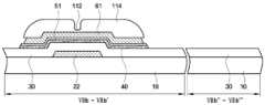
도 7a는 도 1a의 액정 패널에 포함되는 제1 표시판의 배치도이다.FIG. 7A is a layout view of a first display panel included in the liquid crystal panel of FIG. 1A.
도 7b는 도 7a의 제1 표시판을 VIIb-VIIb' 선으로 절개한 단면도이다.FIG. 7B is a cross-sectional view of the first display panel of FIG. 7A taken along the line VIIb-VIIb ′. FIG.
도 8 내지 도 17은 본 발명의 일 실시예에 따른 제1 표시판의 공정 과정을 나타내는 단면도이다.8 to 17 are cross-sectional views illustrating a process of a first display panel according to an exemplary embodiment of the present invention.
도 18a는 도 1b의 제1 변형 실시예를 나타낸 부분 평면도이다.18A is a partial plan view of a first modified embodiment of FIG. 1B.
도 18b는 도 18a의 액정 패널을 B-B' 선으로 절개한 단면도이다.18B is a cross-sectional view of the liquid crystal panel of FIG. 18A taken along line BB ′.
도 19a는 도 1b의 제2 변형 실시예를 나타낸 부분 평면도이다.19A is a partial plan view of a second modified embodiment of FIG. 1B.
도 19b는 도 19a의 액정 패널을 C-C' 선으로 절개한 단면도이다.19B is a cross-sectional view taken along the line CC ′ of the liquid crystal panel of FIG. 19A.
도 20a는 도 1b의 제3 변형 실시예를 나타낸 부분 평면도이다.20A is a partial plan view of a third modified embodiment of FIG. 1B.
도 20b는 도 20a의 액정 패널을 D-D' 선으로 절개한 단면도이다.20B is a cross-sectional view of the liquid crystal panel of FIG. 20A taken along the line D-D '.
<도면의 주요부분에 대한 부호의 설명><Description of the symbols for the main parts of the drawings>
1: 액정 패널 2: 제1 표시판1: liquid crystal panel 2: first display panel
3: 제2 표시판 4: 액정3: second display panel 4: liquid crystal
5: 봉인제 7: 제1 영역5: Sealant 7: First Zone
8: 제2 영역 9: 액정 주입구8: second region 9: liquid crystal injection hole
10: 제1 절연 기판 21: 게이트 선10: first insulating substrate 21: gate line
22: 게이트 전극 30: 게이트 절연막22: gate electrode 30: gate insulating film
40: 반도체층 50:저항성 접촉층40: semiconductor layer 50: ohmic contact layer
55, 56: 저항성 접촉층 패턴 62: 데이터선55, 56: ohmic contact layer pattern 62: data line
65: 소스 전극 66: 드레인 전극65
70: 보호막 81: 화소 전극70: protective film 81: pixel electrode
91, 191, 291, 391: 제어 패턴 92, 192, 292, 392: 공간부91, 191, 291, 391:
93: 만입부 200: 액정 주입기93: indent 200: liquid crystal injector
210: 챔버 220: 액정 용기210: chamber 220: liquid crystal container
본 발명은 액정 표시 장치에 관한 것으로서, 더욱 상세하게는 액정 주입 공정시 액정 및 봉인제의 흐름을 원활하게 하는 제어 패턴을 구비한 액정 표시 장치에 관한 것이다.The present invention relates to a liquid crystal display device, and more particularly, to a liquid crystal display device having a control pattern for smoothly flowing the liquid crystal and the sealing agent during the liquid crystal injection process.
액정 표시 장치(Liquid Crystal Display : LCD)는 현재 가장 널리 사용되고 있는 평판 표시 장치(Flat Panel Display : FPD) 중 하나로서, 전극이 형성되어 있는 두 장의 기판과 그 사이에 삽입되어 있는 액정으로 이루어져, 전극에 전압을 인가하여 액정의 액정 분자들을 재배열시킴으로써 투과되는 빛의 양을 조절하는 표시 장치이다.Liquid crystal display (LCD) is one of the most widely used flat panel display (FPD), which consists of two substrates on which electrodes are formed and a liquid crystal inserted between them. The display device controls the amount of light transmitted by rearranging liquid crystal molecules of a liquid crystal by applying a voltage to the liquid crystal.
액정 표시 장치에 포함되는 두 장의 기판 중 하나인 제1 표시판은 절연 기판 위에 다수의 배선이 형성된다. 이와 같은 다수의 배선을 형성하기 위하여 구성 물질을 적층하고, 마스크 공정을 통해 패터닝하는 사진 식각 방법을 사용하는데, 이러한 사진 식각 방법은 박막 증착, 포토레지스트 도포, 마스크 정렬, 노광, 현상, 식각, 스트립 등의 공정 등의 다수의 공정이 수반되기 때문에, 공정 시간의 증가와 제품 원가 상승의 원인이 된다.In the first display panel, which is one of two substrates included in the liquid crystal display, a plurality of wirings are formed on an insulating substrate. In order to form such a plurality of wirings, a photolithography method of stacking constituent materials and patterning through a mask process is used. Such photolithography methods include thin film deposition, photoresist coating, mask alignment, exposure, development, etching, and stripping. Since many processes, such as these processes, are involved, it becomes a cause of the increase of a process time and a raise of a product cost.
이와 같은 다수의 공정 중에서 마스크 공정의 수를 감소시키기 위한 방법으로 리프트 오프(lift off) 방식을 이용한다. 제1 표시판을 제조하는 공정에는 상면이 도전 물질로 덮인 포토 레지스트 패턴을 제거하는 공정을 포함하고 있으며, 이때 스트리퍼를 사용하여 포토 레지스트 패턴을 제거한다. 포토 레지스트 패턴을 효과적으로 제거하기 위하여, 포토레지스트 패턴의 아래에 위치하는 보호막을 과식각하여 포토레지스트 패턴이 충분한 언더컷을 형성하도록 하여야 한다.Among the many processes, a lift off method is used as a method for reducing the number of mask processes. The process of manufacturing the first display panel includes a process of removing the photoresist pattern on which the top surface is covered with the conductive material, wherein the photoresist pattern is removed using a stripper. In order to effectively remove the photoresist pattern, the protective film under the photoresist pattern should be overetched so that the photoresist pattern forms a sufficient undercut.
한편, 포토 레지스트 패턴을 효과적으로 제거하기 위하여, 제1 표시판에 일종의 제어 패턴을 추가하기도 한다. 그러나, 이와 같은 제어 패턴은 액정 주입 공정에서 액정이나 봉인제의 흐름을 저해하여 액정 패널의 불량률이 높아지는 문제가 발생하면서, 액정이나 봉인제의 흐름을 방해하지 않으면서 포토 레지스트 패턴을 효과적으로 제거할 수 있는 제어 패턴이 필요하게 되었다.In order to effectively remove the photoresist pattern, a kind of control pattern may be added to the first display panel. However, such a control pattern inhibits the flow of the liquid crystal or the sealant in the liquid crystal injection process, thereby increasing the defect rate of the liquid crystal panel, and effectively removing the photoresist pattern without disturbing the flow of the liquid crystal or the sealant. There is a need for a control pattern.
본 발명이 이루고자 하는 기술적 과제는 액정 주입 공정시 액정 및 봉인제의 흐름을 원활하게 하는 제어 패턴을 포함하는 액정 표시 장치를 제공하고자 하는 것이다.An object of the present invention is to provide a liquid crystal display device including a control pattern for smoothly flowing the liquid crystal and the sealing agent during the liquid crystal injection process.
본 발명의 기술적 과제들은 이상에서 언급한 기술적 과제로 제한되지 않으며, 언급되지 않은 또 다른 기술적 과제들은 아래의 기재로부터 당업자에게 명확하게 이해될 수 있을 것이다.The technical objects of the present invention are not limited to the technical matters mentioned above, and other technical subjects not mentioned can be clearly understood by those skilled in the art from the following description.
상기 기술적 과제를 달성하기 위한 본 발명의 일 실시예에 따른 액정 표시 장치는 절연 기판과, 상기 절연 기판 상에 형성된 다수의 박막 트랜지스터,According to an aspect of the present invention, a liquid crystal display device includes an insulating substrate, a plurality of thin film transistors formed on the insulating substrate,
상기 다수의 박막 트랜지스터가 형성되어 있는 영역 외부에 형성되어 있는 액정 주입구과, 상기 액정주입구 상에 형성되어 있는 다수개의 제어 패턴을 포함하는 제1 표시판과, 상기 제1 표시판에 대향하여 배치되는 제2 표시판을 포함한다.A first display panel including a liquid crystal injection hole formed outside an area where the plurality of thin film transistors are formed, a plurality of control patterns formed on the liquid crystal injection hole, and a second display panel disposed to face the first display panel It includes.
기타 실시예들의 구체적인 사항들은 상세한 설명 및 도면들에 포함되어 있다.The details of other embodiments are included in the detailed description and drawings.
본 발명의 이점 및 특징, 그리고 그것들을 달성하는 방법은 첨부되는 도면과 함께 상세하게 후술되어 있는 실시예들을 참조하면 명확해질 것이다. 그러나 본 발명은 이하에서 개시되는 실시예들에 한정되는 것이 아니라 서로 다른 다양한 형태로 구현될 수 있으며, 단지 본 실시예들은 본 발명의 개시가 완전하도록 하고, 본 발명이 속하는 기술분야에서 통상의 지식을 가진 자에게 발명의 범주를 완전하게 알려주기 위해 제공되는 것이며, 본 발명은 청구항의 범주에 의해 정의될 뿐이다. 명세서 전체에 걸쳐 동일 참조 부호는 동일 구성 요소를 지칭한다.Advantages and features of the present invention and methods for achieving them will be apparent with reference to the embodiments described below in detail with the accompanying drawings. However, the present invention is not limited to the embodiments disclosed below, but can be implemented in various different forms, and only the embodiments make the disclosure of the present invention complete, and the general knowledge in the art to which the present invention belongs. It is provided to fully inform the person having the scope of the invention, which is defined only by the scope of the claims. Like reference numerals refer to like elements throughout.
소자(elements) 또는 층이 다른 소자 또는 층의 "위(on)" 또는 "상(on)"으로 지칭되는 것은 다른 소자 또는 층의 바로 위 뿐만 아니라 중간에 다른 층 또는 다른 소자를 개재한 경우를 모두 포함한다. 반면, 소자가 "직접 위(directly on)" 또는 "바로 위"로 지칭되는 것은 중간에 다른 소자 또는 층을 개재하지 않은 것을 나타낸다. 명세서 전체에 걸쳐 동일 참조 부호는 동일 구성 요소를 지칭한다.It is to be understood that when an element or layer is referred to as being "on" or " on "of another element or layer, All included. On the other hand, a device being referred to as "directly on" or "directly above " indicates that no other device or layer is interposed in between. Like reference numerals refer to like elements throughout.
공간적으로 상대적인 용어인 "아래(below)", "아래(beneath)", "하부(lower)", "위(above)", "상부(upper)" 등은 도면에 도시되어 있는 바와 같이 하나의 소자 또는 구성 요소들과 다른 소자 또는 구성 요소들과의 상관관계를 용이하게 기술하기 위해 사용될 수 있다. 공간적으로 상대적인 용어는 도면에 도시되어 있는 방향에 더하여 사용시 또는 동작시 소자의 서로 다른 방향을 포함하는 용어로 이해되어야 한다. 명세서 전체에 걸쳐 동일 참조 부호는 동일 구성 요소를 지칭한다.The terms spatially relative, "below", "beneath", "lower", "above", "upper" May be used to readily describe a device or a relationship of components to other devices or components. Spatially relative terms should be understood to include, in addition to the orientation shown in the drawings, terms that include different orientations of the device during use or operation. Like reference numerals refer to like elements throughout.
이하 첨부된 도면을 참조하여 본 발명의 실시예들을 상세히 설명한다.Hereinafter, embodiments of the present invention will be described in detail with reference to the accompanying drawings.
도 1a 내지 도 2b를 참조하여, 본 발명의 일 실시예에 따른 액정 표시 장치에 대하여 상세히 설명한다. 도 1a는 본 발명의 일 실시예에 따른 액정 패널의 사시도이고, 도 1b는 도 1a의 액정 패널의 A 부분의 확대도이고, 도 2a는 도 1a의 액정 패널에 포함되는 제1 표시판의 평면도이고, 도 2b는 도 2a의 제1 표시판을 A-A' 선으로 절개한 단면도이다.1A to 2B, a liquid crystal display according to an exemplary embodiment of the present invention will be described in detail. FIG. 1A is a perspective view of a liquid crystal panel according to an exemplary embodiment of the present invention, FIG. 1B is an enlarged view of a portion A of the liquid crystal panel of FIG. 1A, and FIG. 2A is a plan view of a first display panel included in the liquid crystal panel of FIG. 1A. 2B is a cross-sectional view of the first display panel of FIG. 2A taken along line AA ′.
본 발명의 일실시예에 따른 액정 표시 장치는 제1 표시판(2), 제1 표시판(3) 및 액정(4)을 포함하는 액정 패널(1)과 액정 패널(1)에 빛을 공급하는 백라이트 어셈블리(미도시) 등을 포함하여 구성된다.The liquid crystal display according to the exemplary embodiment of the present invention includes a
액정 패널(1)은 전기적 신호를 인가 받아 화면에 영상을 표시하는 역할을 하며, 제1 표시판(2)과 제2 표시판(3)이 일정한 간격을 두고 서로 대향하여 부착되며, 양 표시판 사이에 형성된 공간에 일정한 방향으로 배향되어 있는 액정(4)을 포함하여 구성된다.The
이와 같은 액정 패널(1)은 박막 트랜지스터 어레이가 형성되어 있는 제1 영역(7)과 제1 영역(7)의 가장자리에 위치하는 제2 영역(8)으로 구분된다. 이하 상세한 설명에서 기술되는 제1 영역(7)과 제2 영역(8)은 액정 패널(1) 상의 영역 구분에도 사용될 수 있으나, 제1 표시판(2)이나 제2 표시판(3)에서도 동일한 의미로 기술한다.The
제1 영역(7)은 액정 패널(1) 중에서 영상을 표시하는 영역을 말하며, 제2 영역(8)은 액정 패널(1) 제조 공정 상의 마진이 된다. 이러한 제2 영역(8) 상에는 제1 표시판(2)의 제조 공정의 효율을 높이기 위한 제어 패턴(91)을 포함한다. 제어 패턴(91)은 후술할 액정 주입 공정시에 액정(4)과 봉인제(5)가 원활하게 유동할 수 있도록 형성되어야 한다.The
제어 패턴(91)은 제1 영역(7)과 제2 영역(8) 사이의 높이 차이를 줄여 후술할 포토 레지스트 패턴(122)이 효과적으로 제거되도록 하는 역할을 한다. 이러한 제어 패턴(91)은 일정한 높이를 갖는 격벽으로 되어 횡단면이 스트라이프(stripe)이며, 제1 절연 기판(10) 상부로 돌출되어 있다. 제어 패턴(91)의 사이에는 공간부(92)가 형성된다. 이러한 제어 패턴(91)은 제1 영역(7)과 외부 영역을 가로질러 제2 영역(8)에 형성된다. 즉, 제어 패턴(91)은 제1 영역(7)에서 외부 영역 방향으로 스트라이프가 형성된다. 또한, 제어 패턴(91)의 길이(L)는 제2 영역(8)의 폭과 거의 같은 1~2mm로 형성되는 것이 바람직하며, 제어 패턴(91)의 폭(d)은 50~100㎛ 정도로 형성하는 것이 바람직하다.The
또한, 제어 패턴(91)은 제1 영역(7)과 제2 영역(8) 간의 높이차를 해소할 뿐만 아니라, 액정 주입 공정시 액정(4) 또는 봉인제(5) 등의 흐름을 원활하게 해야 하므로 내부에 만입부(93)를 형성할 수 있다. 제어 패턴(91) 상으로 주입된 액정 또는 봉인제(5)는 만입부(93)를 통하여 외부에서 제1 영역(7) 방향으로 원활하게 이동할 수 있다.In addition, the
공간부(92)는 각 제어 패턴(91) 사이에 형성된 공간을 말하는 것으로서, 제1 영역(7)과 외부 영역을 직접 연결하는 부분이 된다. 즉, 액정(4)이나 봉인제(5)를 주입하는 과정에서 액정(4)이나 봉인제(5)는 제어 패턴(91)의 저항에 의해서 흐름이 원활하지 못하기 때문에, 이 같은 저항을 줄이기 위하여 제어 패턴(91) 사이에 일정한 공간부(92)를 형성한다. 제1 표시판(2)과 제2 표시판(3) 사이의 간격은 매우 작기 때문에 액정(4)이나 봉인제(5)가 유동할 때 제어 패턴(91)는 매우 큰 저항이 될 수 있다. 따라서, 이러한 공간부(92)와 만입부(93)는 실질적으로 액정(4)이나 봉인제(5) 주입시에 발생하는 저항을 효과적으로 감소시킬 수 있다. 이와 같은 제어 패턴(91)은 제1 영역(7)과 제2 영역(8) 간의 높이차를 해소 및 액정(4)이나 봉인제(5)의 저항 등을 고려할 때, 제어 패턴(91)의 높이는 0.2~1.0㎛ 정도가 바람직하다.The
이와 같은, 제어 패턴(91)은 게이트 절연막(30)과 보호막(70) 형성시 함께 형성될 수 있다. 즉, 게이트 절연막(30)과 보호막(70)의 이중층으로 형성될 수도 있으며, 게이트 절연막(30)이나 보호막(70) 중 어느 한 층을 이용하여 형성될 수도 있다. 이밖에 필요에 따라, 제어 패턴(91)은 게이트 배선(21, 22), 데이터 배선(62, 65, 66) 또는 반도체층(40)과 같은 물질로 함께 형성될 수 있다.As such, the
한편, 제어 패턴(91)은 제2 영역(8) 전체에 형성될 수 있으나, 적어도 액정 주입구(9)에 형성되는 것이 바람직하다.The
또한, 제2 영역(8)에는 제1 표시판(2)과 제2 표시판(3)을 부착하고, 액정(4)의 유출을 방지하기 위한 봉인제(5)가 도포된다. 액정 주입 공정시 액정 패널(1)의 제2 영역(8)은 액정 주입구(9)를 제외한 모든 영역에 봉인제(5)가 도포되며, 봉인제(5)가 도포된 액정 패널(1)은 내부를 진공으로 유지한 후 액정 용기(220, 도3 참조)에 담기게 된다. 액정 주입 공정에 관해서는 구체적으로 후술한다.In addition, the
제1 표시판(2)은 진공 증착 등의 방법으로 형성된 박막을 이용하여 만들어진 트랜지스터로서, 전기 신호를 액정에 기록 가능하도록 스위치 역할을 하는 것으로서, 그 구체적인 구성요소는 제조 방법과 함께 구체적으로 후술한다.The
제2 표시판(3)은 백라이트 어셈블리(미도시)를 통하여 공급되는 빛이 컬러 필터(미도시)를 투과하여 소정의 영상을 표시하도록 하는 역할을 한다. 이와 같은 제2 표시판(3)은 제2 절연 기판 상에 색상을 구현하는 컬러 필터, 컬러 필터의 셀(cell) 사이를 구분하고 빛을 차단하는 블랙 메트릭스(black matrix), 및 액정 셀에 전압을 인가하기 위한 투명 전극인 공통 전극(미도시)을 포함하여 구성된다.The
백라이트 어셈블리(미도시)는 액정 패널에 빛을 공급하는 역할을 한다. 이와 같은 백라이트 어셈블리(미도시)는 빛을 방출하는 램프를 포함하며, 램프의 배열 위치에 따라 램프가 도광판의 측면에 위치하는 엣지(edge)형과 램프가 확산판의 하부에 위치하는 직하형으로 구분된다.The backlight assembly (not shown) serves to supply light to the liquid crystal panel. Such a backlight assembly (not shown) includes a lamp that emits light. The backlight assembly (not shown) includes an edge type in which the lamp is located at the side of the light guide plate and a direct type in which the lamp is located below the diffuser plate, depending on the arrangement of the lamps. Are distinguished.
이하, 도 3 내지 도 6을 참조하여, 본 발명의 일 실시예에 따른 액정 표시 장치의 액정 주입 공정에 대하여 상세히 설명한다. 도 3 내지 도 6은 액정 패널에 액정을 주입하는 공정의 단계별 공정도이다.Hereinafter, the liquid crystal injection process of the liquid crystal display according to the exemplary embodiment of the present invention will be described in detail with reference to FIGS. 3 to 6. 3 to 6 are step-by-step process diagrams of a process of injecting liquid crystal into a liquid crystal panel.
본 발명에 따른 액정 표시 장치의 액정 주입 공정은, 우선 제1 표시판(2) 및 공통 기판 표시판(3)의 둘레에 액정 주입구(9)를 갖도록 봉인제(5)를 도포한다. 그 다음에 액정 패널(1)의 내부를 진공으로 만들고, 액정 주입구(9)가 액정에 완전히 잠기도록 액정 패널(1)을 액정 용기(220)에 담가 액정을 주입하는 방식이다. 이에 대하여 각 단계별로 도면을 참조하여 구체적으로 설명한다.In the liquid crystal injection process of the liquid crystal display device which concerns on this invention, the sealing
우선, 도 3 및 도 1a를 참조하면, 제1 표시판(2)과 제2 표시판(3)에 액정을 배향하기 위한 배향처리 공정을 하고, 제1 표시판(2)과 제2 표시판(3) 사이의 간격을 유지시키기 위한 스페이서(미도시)을 산포한다.First, referring to FIGS. 3 and 1A, an alignment process for aligning liquid crystals is performed on the
그 다음에 두 표시판 중에 적어도 하나의 표시판에 액정의 유출을 방지하기 위한 봉인제(5)를 도포한 후 두 기판을 핫 프레스(hot press) 공정을 통하여 결합 한다. 이렇게 결합된 액정 패널(1)을 액정 주입기(200)의 챔버(210) 안으로 로딩한다.Next, after applying the
다음으로, 챔버(210) 내부의 공기를 배출하여 챔버(210) 내부를 고진공 상태로 만들면, 봉인제(5)로 둘러싸인 액정 패널(1)의 내부도 챔버(210)의 내부와 같이 고진공 상태를 유지하게 된다.Next, when the air inside the
다음으로, 도 4에 도시된 바와 같이, 챔버(210)를 외부와 격리되도록 밀폐시켜 챔버(210) 내부의 고진공 상태를 유지시킨다. 이와 같이 챔버(210) 내부를 고진공 상태로 유지시키면서, 액정 주입구(9)가 액정(4)에 완전히 잠기도록 액정 패널(1)을 액정 용기(220)에 담근다. 이 때에는 액정 패널(1)의 내부와 외부의 압력이 같기 때문에 액정 패널(1) 내부로 액정(4)이 주입되지 않는다. Next, as shown in FIG. 4, the
다음으로, 도 5에 도시된 바와 같이, 챔버(210)의 내부에 기체를 주입하여 챔버(210)의 내부를 저진공 또는 상압 상태로 만든다. 상기 기체는 N2 일 수 있다. 챔버(210)의 내부가 저진공 또는 상압 상태가 되더라도, 봉인제(5)로 둘러싸인 액정 패널(1)의 내부는 고진공 상태를 유지하게 된다. 따라서, 액정 패널(1)의 내외부 사이에 압력차가 발생하게 되며, 이와 같은 압력차에 의하여 액정(4)은 액정 주입구(9)를 통하여 액정 패널(1)의 내부로 주입된다. 이 때 제1 표시판(2)의 제2 영역(8)에 형성된 제어 패턴(91)은 공간부(92)포함하고 있어, 액정(4)의 흐름을 원활하게 하여 액정(4) 주입 시간을 단축시키며 깨끗하게 주입되도록 한다.Next, as shown in FIG. 5, gas is injected into the
다음으로, 도 6에서 보는 바와 같이, 챔버(210) 내부를 상압으로 유지한 채, 액정(4)으로 가득찬 액정 패널(1)을 액정 용기(220)로부터 꺼내어 액정 주입구(9) 를 봉인하면 액정 주입 공정이 끝나게 된다. 이때, 액정 주입구(9)를 봉인하는 과정에서 봉인제(5)는 제어 패턴(91)이 형성된 제2 영역(8) 상으로 원활하게 유입된다.Next, as shown in FIG. 6, when the inside of the
이하, 도 7a 및 도 7b를 참조하여 제1 표시판에 대해 상세히 설명한다. 도 7a는 도 1a의 액정 패널에 포함되는 제1 표시판의 배치도이고, 도 7b는 도 7a의 제1 표시판을 VIIb-VIIb' 선으로 절개한 단면도이다.Hereinafter, the first display panel will be described in detail with reference to FIGS. 7A and 7B. FIG. 7A is a layout view of a first display panel included in the liquid crystal panel of FIG. 1A, and FIG. 7B is a cross-sectional view of the first display panel of FIG. 7A taken along line VIIb-VIIb ′.
제1 표시판(2)은 제1 절연 기판(10) 위에 형성된 게이트 배선(21, 22), 게이트 절연막(30), 반도체층(40), 저항성 접촉층 패턴(55, 56), 데이터 배선(62, 65, 66), 보호막(70), 제어 패턴(91) 및 화소 전극(81) 등을 포함한다.The
제1 절연 기판(10)은 투명 유리 또는 플라스틱과 같이 내열성 및 투광성을 갖는 재질로 형성된다.The first insulating
제1 절연 기판(10) 위에는 게이트 배선(21, 22) 이 형성되며, 두 배선은 제1 절연 기판(10) 위의 같은 층(layer)에 함께 형성될 수 있다. 이와 같은 게이트 배선(21, 22)은 알루미늄(Al)과 알루미늄 합금 등 알루미늄 계열의 금속, 은(Ag)과 은 합금 등 은 계열의 금속, 구리(Cu)와 구리 합금 등 구리 계열의 금속, 몰리브덴(Mo)과 몰리브덴 합금 등 몰리브덴 계열의 금속, 크롬(Cr), 티타늄(Ti), 탄탈륨(Ta) 등의 금속성 재료로 이루어질 수 있다. 또한, 게이트 배선(21, 22)과 물리적 성질이 다른 두 개의 도전막(미도시)을 포함하는 다중막 구조를 가질 수 있다.
여기서 게이트 배선(21, 22)은 제1 절연 기판(10)의 제1 방향으로 배치된 게이트 선(21)과 게이트 선(21)에 돌기의 형태로 이루어진 게이트 전극(22)을 말하는 것이다.Here, the gate lines 21 and 22 refer to the
구체적으로, 게이트 배선(21, 22)은 예를 들면 가로 방향과 같은 제1 방향으로 배열되어 게이트 신호를 전달하는 게이트 선(21)과 게이트 선(21)에서 돌기 형태로 돌출되어 형성된 게이트 전극(22)을 포함하며, 게이트 전극(22)은 후술하는 소스 전극(65) 및 드레인 전극(66)과 함께 박막 트랜지스터의 단자를 구성하게 된다.Specifically, the
한편, 게이트 배선(21, 22) 은 도전성 유기 고분자계 물질인 PEDOT(PolyEthyleneDiOxyThiophene)를 코팅 방법으로 도포하거나 또는 인젝트-프린팅 방법으로 인쇄하여 형성될 수도 있다.The gate lines 21 and 22 may be formed by coating PEDOT (PolyEthyleneDiOxyThiophene), which is a conductive organic polymer material, by a coating method or by printing by an inject-printing method.
게이트 배선(21, 22) 및 제1 절연 기판(10) 위에는 실리콘 산화물(SiOx) 또는 실리콘 질화물(SiNx)등의 무기 절연 물질, BCB(BenzoCycloButene), 아크릴계 물질, 폴리이미드와 같은 유기 절연 물질로 이루어진 게이트 절연막(30)이 게이트 배선(21, 22)을 덮고 있다.On the gate wirings 21 and 22 and the first insulating
이와 같은 게이트 절연막(30)은 화소 영역을 노출하도록 형성될 수 있다. 여기서, 화소 영역이란 게이트 배선(21, 22)과 데이터 배선(62, 65, 66)에 의해 정의되고, 제1 표시판(2)이 사용되는 액정 표시 장치(1)에서 백라이트 어셈블리로(미도시)부터 출사된 빛이 통과하는 영역으로 이해될 수 있다.The
게이트 절연막(30) 상부의 일부에는 수소화 비정질 규소(hydrogenated amorphous silicon), 다결정 규소 또는 도전성 유기물질 등으로 이루어진 반도체층(40)이 형성되어 있다.A
반도체층(40)은 섬형, 선형 등과 같이 다양한 형상을 가질 수 있으며, 예를 들어 본 실시예에서와 같이 선형으로 형성되는 경우, 데이터선(62) 아래에 위치하여 게이트 전극(22) 상부까지 연장된 형상을 가질 수 있다. 본 실시예의 반도체층(40)은 게이트 전극(22), 후술하는 데이터 배선(62, 65, 66)을 실질적으로 전부 오버랩할 수 있다. 즉, 반도체층(40)은 소스 전극(65) 및 드레인 전극(66)보다 돌출되어 형성될 수 있다. 그러나, 반도체층(40)의 모양은 선형에 한정되지 않고 다양하게 변형될 수 있다. 반도체층(40)이 섬형으로 형성된 경우, 반도체층(40)은 게이트 전극(22) 상에서 게이트 전극(22)과 오버랩되며, 소스 전극(65) 및 드레인 전극(66)의 적어도 일부 오버랩 될 수 있다. 이러한 반도체층(40)은 박막 트랜지스터의 채널 영역을 제외하고 데이터 배선(62, 65, 66)과 실질적으로 동일하게 형성될 수 있다.The
반도체층(40)의 상부에는 실리사이드(silicide) 또는 n형 불순물이 고농도로 도핑되어 있는 n+ 수소화 비정질 규소 또는 p형 불순물이 도핑되어 있는 ITO 따위의 물질로 이루어진 저항성 접촉층 패턴(ohmic contact layer pattern)(55. 56)이 형성될 수 있다. 저항성 접촉층 패턴(55, 56)은 쌍(pair)을 이루어 반도체층(40) 위에 위치하여, 후술하는 소스 전극(65) 및 드레인 전극(66)과 반도체층(40)의 접촉 특성을 양호하게 한다. 반도체층(40)과, 반도체층(40) 상부에 형성되는 소스 전극(65) 및 드레인 전극(66)의 접촉 특성이 양호한 경우에는 저항성 접촉층 패턴(55, 56)은 생략될 수 있다.An ohmic contact layer pattern made of a material such as n + hydrogenated amorphous silicon doped with a high concentration of silicide or n-type impurities or ITO doped with p-type impurities on the
저항성 접촉층 패턴(55, 56) 및 게이트 절연막(30) 위에는 데이터 배선(62, 65, 66) 및 드레인 전극(66)이 형성된다. 여기서 데이터 배선(62, 65, 66)은 데이터 선(62), 소스 전극(65) 및 드레인 전극(66)을 말한다.The data lines 62, 65, 66, and the
데이터 선(62)은 세로 방향 등과 같은 제2 방향으로 배열되어 게이트 선(21)과 교차하도록 배치되며, 데이터 신호를 인가 받아 소스 전극(65)으로 전달한다. 이러한 데이터 선(62)은 제2 방향으로 평행하게 다수개가 구비되어 있다. 각각의 데이터선(62)은 게이트선(22)과 교차할 수 있다.The
소스 전극(65)은 데이터 선(62)으로부터 분지되어 일단부가 데이터 선(62)에 연결되어 있으며, 타단부는 반도체층(40)의 상부에 위치하여 반도체층(40)과 중첩되도록 배치된다.The
드레인 전극(66)은 일단부가 반도체층(40) 상부에 위치하여 반도체층(40)과 일부가 중첩되도록 배치되며, 게이트 전극(22)을 중심으로 소스 전극(65)과 대향되도록 일정 간격 이격하여 형성된다.One end of the
이와 같은 소스 전극(65)과 드레인 전극(66)은 전술한 게이트 전극(22)과 함께 스위칭 소자를 이루게 되어, 게이트 전극(22)에 전압이 인가되면 소스 전극(65)과 드레인 전극(66) 사이에 전류가 흐르게 된다.The
한편, 데이터 배선(62, 65, 66)은 알루미늄, 크롬, 몰리브덴, 탄탈륨 및 티타늄 등 중에서 하나 이상의 물질로 구성된 단일막 또는 다층막으로 이루어질 수 있다. 즉, 데이터 배선(62, 65, 66)은 크롬, 몰리브덴 계열의 금속, 탄탈륨 및 티타늄 등 내화성 금속으로 이루어지는 것이 바람직하며, 내화성 금속 따위의 하부막(미도시)과 그 위에 위치한 저저항 물질 상부막(미도시)으로 이루어진 다층막 구 조를 가질 수 있다. 다층막 구조의 예로는 앞서 설명한 크롬 하부막과 알루미늄 상부막 또는 알루미늄 하부막과 몰리브덴 상부막의 이중막 외에도 몰리브덴막-알루미늄막-몰리브덴막의 삼중막을 들 수 있다.The data lines 62, 65, and 66 may be formed of a single film or a multilayer film made of one or more materials among aluminum, chromium, molybdenum, tantalum, titanium, and the like. That is, the data lines 62, 65, and 66 are preferably made of refractory metals such as chromium, molybdenum-based metals, tantalum, and titanium, and include a lower layer (not shown) such as a refractory metal and an upper layer of a low resistance material disposed thereon. It may have a multilayer film structure consisting of (not shown). Examples of the multilayer structure include a triple layer of a molybdenum film-aluminum film-molybdenum film in addition to the chromium lower film and the aluminum upper film or the aluminum lower film and the molybdenum upper film.
데이터 배선(62, 65, 66) 및 노출된 반도체층(40)의 위에는 절연막으로 이루어진 보호막(70)이 도포된다. 보호막(70)은 질화규소 또는 산화규소로 이루어진 무기물, 평탄화 특성이 우수하며 감광성(photosensitivity)을 가지는 유기물 또는 플라스마 화학 기상 증착(plasma enhanced chemical vapor deposition, PECVD)으로 형성되는 a-Si:C:O, a-Si:O:F 등의 저유전율 절연 물질 등으로 이루어진다. 또한, 보호막(70)을 유기 물질로 형성하는 경우에는 소스 전극(65)과 드레인 전극(66) 사이의 반도체층(40)이 드러난 부분에 보호막(70)의 유기 물질이 접촉하는 것을 방지하기 위하여, 질화 규소(SiNx) 또는 산화 규소(SiO2)로 이루어진 하부 무기막과 상부 유기막의 이중막 구조를 가질 수 있다.A
제어 패턴(91)은 제1 영역(7)과 제2 영역(8) 사이의 높이 차이를 줄여 후술할 포토 레지스트 패턴(122)이 효과적으로 제거되도록 하는 역할을 하는 것으로서, 구체적인 설명은 전술한 바와 같다.The
화소 전극(81)은 화소 영역에 제1 절연 기판(10)의 바로 위에 형성될 수 있으며, 드레인 전극(66)과 일단부가 연결된 드레인 전극 확장부(67)와 직접 전기적으로 접속된다.The
화소 전극(81)은 화소의 투과율을 조절함으로써, 백라이트 어셈블리(미도시)에서 공급하는 빛을 조절하여 액정 패널에 영상이 표시되도록 한다. 이와 같은 화 소 전극(81)은 화소 전극(81)은 화소 영역에 제1 절연 기판(10)의 바로 위에 형성될 수 있으며, 드레인 전극 확장부(67)와 직접 전기적으로 접속된다. 드레인 전극 확장부(67)를 통하여 데이터 전압이 인가된 화소 전극(81)은 제2 표시판(3)의 공통 전극과 함께 전기장을 생성함으로써, 화소 전극(81)과 공통 전극(미도시) 사이에 개재된 액정 분자들의 배열을 결정한다.The
한편, 화소 전극(81)은 ITO(Indium Tin Oxide) 또는 IZO(Indium Zinc Oxide) 등의 투명 도전체 또는 알루미늄 등의 반사성 도전체로 이루어 진다. 전술한 바와 같이, 화소 전극(81)과 공통 전극(미도시) 사이에 전압이 인가되면 전압에 의해 발생하는 전계의 영향으로 액정이 재배열하게 되며, 이 때 백라이트 어셈블리(미도시)로부터 공급되는 빛이 액정 패널을 투과하게 된다. 그러므로, 화소 전극(81)과 공통 전극 사이에 전압이 인가되지 않으면 액정 패널의 빛이 투과할 수 없게 된다.On the other hand, the
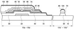
이하, 도 7a 와 도 7b 및 도 8 내지 도 17을 참조하여, 본 발명의 일 실시예에 따른 제1 표시판의 제조 방법에 대하여 상세히 설명한다. 도 8 내지 도 17은 본 발명의 일 실시예에 따른 제1 표시판의 공정 과정을 나타내는 단면도이다.Hereinafter, a method of manufacturing the first display panel according to an exemplary embodiment of the present invention will be described in detail with reference to FIGS. 7A, 7B, and 8 through 17. 8 to 17 are cross-sectional views illustrating a process of a first display panel according to an exemplary embodiment of the present invention.
먼저, 도 8 및 도 7a를 참조하면, 제1 절연 기판(10) 상에 게이트 전극(22)을 포함하는 게이트 배선(21, 22)을 형성한다. 구체적으로, 제1 절연 기판(10) 상에 게이트 도전층을 예컨대 스퍼터링 등을 이용하여 적층한 다음, 이를 사진 식각하여 게이트선(21), 게이트 전극(22)을 형성한다.First, referring to FIGS. 8 and 7A, gate wirings 21 and 22 including the
이어서, 도 9를 참조하면, 상기 결과물 상에 게이트 절연막(30), 수소화 비정질 규소 등으로 이루어진 반도체층(40), 및 실리사이드 또는 n형 불순물이 고농 도로 도핑된 n+ 수소화 비정질 규소 또는 p형 불순물이 도핑되어 있는 ITO 따위의 물질 등으로 이루어진 저항성 접촉층(50)을 적층한다. 게이트 절연막(30), 반도체층(40) 및 저항성 접촉층(50)의 적층은 예컨대, 화학 기상 증착(Chemical Vapor Deposition; CVD)으로 이루어질 수 있다.Next, referring to FIG. 9, the
이어서, 저항성 접촉층(50) 상에 예컨대 스퍼터링 등을 이용하여 데이터 배선용 도전층(60)을 적층하고, 포토레지스트층(110)을 도포한다.Next, the
이와 같은, 게이트 절연막(30), 반도체층(40), 저항성 접촉층(50),(데이터 배선용 도전층(60) 및 포토레지스트층(110)은 제1 표시판(2)의 제1 영역(7) 뿐만 아니라 제2 영역(8)에도 적층된다.The
이어서, 도 10 및 도 7b를 참조하면, 포토레지스트층(110)을 패터닝하여 데이터 배선용 도전층(60) 상에 데이터 배선 형성용 포토레지스트 패턴(112)을 형성한다. 데이터 배선 형성용 포토레지스트 패턴(112)은 소스 전극(65)과 드레인 전극(66)의 이격 공간을 덮는다. 상술한 바와 같은 영역별로 다른 두께를 갖는 데이터 배선 형성용 포토레지스트 패턴(112)은 슬릿 마스크 또는 하프톤 마스크를 이용하여 형성될 수 있다.Next, referring to FIGS. 10 and 7B, the
이어서, 도 11 및 도 7b를 참조하면, 데이터 배선 형성용 포토레지스트 패턴(112)을 식각마스크로 이용하여 노출된 데이터 배선용 도전층(60)을 식각한다. 데이터 배선용 도전층(60)의 식각은 데이터 배선용 도전층(60)의 종류, 두께 등에 따라 다르지만, 바람직한 일예로서 습식 식각으로 진행될 수 있다. 그 결과, 데이터선(62) 및 데이터 배선용 도전층 패턴(61)이 형성된다. 한편, 채널 영역의 소스 전극(65) 및 드레인 전극(66)의 패턴은 완성되지 않으며, 이 영역에서 데이터 배선용 도전층 패턴(61)은 분리되지 않고 여전히 일체형으로 잔류한다.Next, referring to FIGS. 11 and 7B, the exposed data wiring
이어서, 도 12 및 도 2b를 참조하면, 데이터 배선용 도전층 패턴(61)의 형성에 따라 노출된 저항성 접촉층(50) 및 그 하부의 반도체층(40)을 식각하여 미완성 저항성 접촉층 패턴(51) 및 그 하부의 미완성 반도체층(40)을 형성한다. 저항성 접촉층(50) 및 반도체층(40)의 식각은 예컨대, 건식 식각으로 진행될 수 있다. 저항성 접촉층(50) 및 반도체층(40)의 식각 결과 게이트 절연막(30)이 노출된다.Next, referring to FIGS. 12 and 2B, the exposed
이어서, 도 13, 도 12및 도 7b를 참조하면, 데이터 배선 형성용 포토레지스트 패턴(112)을 제거하여 하부의 데이터 배선용 도전층 패턴(61)을 노출한다. 두께가 얇은 데이터 배선 형성용 포토레지스트 패턴(112)은 예를 들어 산소 등을 이용한 애슁 공정에 의해 제거할 수 있다. 한편, 상술한 저항성 접촉층(50) 및 반도체층(40)의 식각 단계에서 데이터 배선 형성용 포토레지스트 패턴(112)이 이미 제거될 수도 있으며, 이 경우 애슁 공정은 생략될 수 있다.13, 12, and 7B, the
이어서, 도 14, 도 13 및 도 7b를 참조하면, 두께가 두꺼운 데이터 배선 형성용 포토레지스트 패턴(114)을 식각마스크로 이용하여 노출되어 있는 채널 영역의 데이터 배선용 도전층 패턴(61)을 식각한다. 그 결과 소스 전극(65), 드레인 전극(66) 및 드레인 전극 확장부(67)가 형성되며, 소스 전극(65)과 드레인 전극(66)의 이격 공간 사이로 미완성 저항성 접촉층 패턴(51)이 노출된다. 계속해서, 노출된 미완성 저항성 접촉층 패턴(51)을 식각하여 분리한다. 그 결과, 저항성 접촉층 패턴(55, 56)이 완성된다. 또한, 반도체층(40)의 일부도 식각되어 완성된다.14, 13, and 7B, the
이어서, 도 15를 참조하면, 상기 결과물 상에 예컨대 CVD를 이용하여 보호막(70)을 적층한다.Next, referring to FIG. 15, a
이어서, 도 16, 도 15 및 도 7b를 참조하면, 보호막(70) 상에 포토레지스트 물질을 도포하고 패터닝하여 포토레지스트 패턴(122, 124)을 형성한다. 포토레지스트 패턴(122, 124)는 게이트 배선(21, 22) 상의 보호막(70) 및 드레인 전극 확장부(67)를 제외한 데이터 배선(62, 65, 66) 상의 보호막(70)과 제어 패턴(91)의 형성 위치 상에 형성된다. 포토레지스트 패턴(122, 124)은 마스크로 전부 차단되어 노광되지 않으며, 화소 영역을 노출시킨다.Next, referring to FIGS. 16, 15, and 7B, photoresist materials are coated and patterned on the
또한, 포토레지스트 패턴(122, 124)을 식각마스크로 이용하여 노출된 보호막(70)을 식각한다. 보호막(70)의 식각은 건식 식각으로 진행된다. 보호막(70)은 포토레지스트 패턴(122)의 하부에 드레인 전극 확장부(67)를 일부 노출시키도록 서로 이격되어 형성된다. 이와 함께 게이트 절연막(30)도 식각된다. 식각의 식각 가스는 예를 들어 CF4, SF6, CHF3, O2 또는 이들의 조합을 포함할 수 있으며, 구성 요소의 조합이나 이들 조합의 조성비를 조절함으로써 식각률을 제어할 수 있다.In addition, the exposed
이에 따라 포토 레지스트 패턴(122, 124)이 보호막 패턴(70)보다 돌출되는 언더컷(undercut)이 발생하고, 드레인 전극 확장부(67)의 노출 면적이 증가한다. 상술한 식각의 결과, 드레인 전극 확장부(67)가 노출되고, 화소 영역의 제1 절연 기판(10)이 노출된다. 또한, 제어 패턴(91)이 형성된다.As a result, undercuts occur in which the
이어서, 도 17 및 도 7b를 참조하면, 리프트 오프법을 이용하여 포토 레지스 트 패턴(122, 124) 및 그 상부에 존재하는 화소 전극용 도전 물질(80)을 제거한다. 구체적으로, 예컨대 아민계, 글리콜계 등을 포함하는 스트리퍼를 분사 방식 또는 딥 방식 등으로 상술한 절개 부위로 주입하여 포토레지스트 패턴(122, 124)에 접촉시키면 스트리퍼가 포토레지스트 패턴(122)을 용해시켜 보호막(70)으로부터 포토레지스트 패턴(122)을 박리하며, 동시에 포토레지스트 패턴(122) 상에 존재하는 화소 전극용 도전 물질(80)도 제거한다.Next, referring to FIGS. 17 and 7B, the
이때, 제어 패턴(91)은 스트리퍼가 포토 레지스트 패턴(122, 124)에 용이하게 접촉 될 수 있도록 공간을 형성해주며, 제1 영역(7)과 제2 영역(8) 상이의 높이 차이를 줄여서 양쪽 영역의 스트리퍼의 농도 차이를 줄이게 된다. 따라서 제1 영역(7)과 제2 영역(8)의 모든 영역에 남아있는 포토 레지스트 패턴(122, 124)이 효율적으로 제거된다.In this case, the
상술한 제1 표시판의 제조 방법에서는 게이트 절연막(30) 및 보호막(70)을 이용한 제어 패턴(91)의 형성 방법에 관하여 기술하였으나, 제어 패턴()의 형성 물질에 따라 게이트 배선(21, 22), 데이터 배선(62, 65, 66), 또는 반도체층(40)의 형성 공정에서 제어 패턴(91)을 형성할 수도 있을 것이다. 또한, 제어 패턴(91)에 형성된 만입부(93)는 제어 패턴(91) 형성을 위한 식각 공정에서 함께 형성된다.In the above-described method of manufacturing the first display panel, a method of forming the
이하 도 18a 및 도 18b를 참조하여 본 발명의 제1 변형 실시예에 따른 제1 표시판을 설명한다. 여기서 도 18a는 도 2a의 제1 변형 실시예를 나타낸 부분 평면도이고, 도 18b는 도 18a의 액정 패널을 B-B' 선으로 절개한 단면도이다.Hereinafter, a first display panel according to a first modified embodiment of the present invention will be described with reference to FIGS. 18A and 18B. 18A is a partial plan view illustrating a first modified embodiment of FIG. 2A, and FIG. 18B is a cross-sectional view of the liquid crystal panel of FIG. 18A taken along line BB ′.
본 발명의 제1 변형 실시예에 의한 제1 표시판(2)의 제어 패턴(191)은 제1 영역(7)과 외부를 연결하는 스트라이프 형상으로서, 내부가 채워진 솔리드형으로 형성된다. 액정(4) 또는 봉인제(5) 등의 액상 물질의 흐름을 원활하게 하기 위해서는 제어 패턴(191)의 폭을 좁게 형성하고, 상대적으로 공간부(192)를 넓게 형성할 수 있다.The
이하 도 19a 및 도 19b를 참조하여 본 발명의 제2 변형 실시예에 따른 제1 표시판을 설명한다. 여기서 도 19a는 도 2a의 제2 변형 실시예를 나타낸 부분 평면도이고, 도 19b는 도 19a의 액정 패널을 C-C' 선으로 절개한 단면도이다.Hereinafter, a first display panel according to the second modified embodiment of the present invention will be described with reference to FIGS. 19A and 19B. 19A is a partial plan view illustrating a second modified embodiment of FIG. 2A, and FIG. 19B is a cross-sectional view of the liquid crystal panel of FIG. 19A taken along line C-C ′.
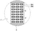
본 발명의 제2 변형 실시예에 의한 제1 표시판(2)의 제어 패턴(291)은 내부에 만입부(293)를 포함하는 스트라이프 형상으로서, 횡단면이 직사각형을 이루게 된다.The
이와 같은 제어 패턴(291)은 제1 영역(7)과 외부 영역 사이에 복수의 열로 배열될 수 있다. 즉, 내부에 만입부(293)를 포함하는 스트라이프형 제어 패턴(291)을 복수개로 분할하여 형성한다. 이와 같이 제어 패턴(291)을 복수개로 분할하면 제1 영역(7)과 외부 영역 사이에 저항이 되는 격벽이 증가하기 때문에 각 제어 패턴(291) 사이에 일정한 간격을 두어 액정(4)이나 봉인제(5)가 흘러들어 갈 수 있도록 하는 것이 바람직하다. 이러한 제어 패턴(291)은 하나의 스트라이프 당 3~5 개로 분할하는 것이 바람직하다. 또한, 제어 패턴(291)의 배열 방식이나 제어 패턴(291) 사이의 공간부(292)의 너비는 제1 표시판(2)의 크기 등에 따라 다양하게 변형할 수 있을 것이다.The
이하 도 20a 및 도 20b를 참조하여 본 발명의 제3 변형 실시예에 따른 제1 표시판을 설명한다. 여기서 도 20a는 도 2a의 제3 변형 실시예를 나타낸 부분 평면도이고, 도 20b는 도 20a의 액정 패널을 D-D' 선으로 절개한 단면도이다.Hereinafter, a first display panel according to a third modified embodiment of the present invention will be described with reference to FIGS. 20A and 20B. 20A is a partial plan view illustrating a third modified embodiment of FIG. 2A, and FIG. 20B is a cross-sectional view of the liquid crystal panel of FIG. 20A taken along line D-D ′.
본 발명의 제3 변형 실시예에 의한 제1 표시판(2)의 제어 패턴(391)은 횡단면이 사각형, 원형 등을 갖는 점형상으로 형성된다.The
제어 패턴(391)은 일정한 단면적을 갖고 점형상으로 매트릭스 타입인 복수의 행과 열로 배열될 수 있다. 제어 패턴(391)을 점형상으로 배열할 경우, 제어 패턴(391) 사이의 간격이 넓어지게 되어 액정(4)이나 봉인제(5)의 유동이 원활해지게 된다. 제어 패턴(391)을 점형상으로 배열함에 있어서, 반드시 배열 방식은 격자 무늬로 배열할 필요는 없다. 다만, 제어 패턴(391)의 총단면적과, 액정(4)이나 봉인제(5) 등의 흐름의 원활함 등을 고려하여 다양한 방식으로 배열할 수 있다. 이 경우 제어 패턴(391)의 적어도 한 변이 90㎛ 이내가 되도록 형성되는 것이 바람직하다.The
이상 첨부된 도면들을 참조하여 본 발명의 실시예들을 설명하였지만, 본 발명이 속하는 기술분야에서 통상의 지식을 가진 자는 본 발명이 그 기술적 사상이나 필수적인 특징을 변경하지 않고서 다른 구체적인 형태로 실시될 수 있다는 것을 이해할 수 있을 것이다. 그러므로 이상에서 기술한 실시예들은 모든 면에서 예시적인 것이며 한정적이 아닌 것으로 이해해야만 한다.While the present invention has been particularly shown and described with reference to exemplary embodiments thereof, it is clearly understood that the same is by way of illustration and example only and is not to be taken by way of limitation, You will understand. It is therefore to be understood that the above-described embodiments are illustrative in all aspects and not restrictive.
상술한 바와 같이, 본 발명의 실시예들에 따른 액정 표시 장치는 액정이 주입되는 액정 주입구 부분에 액정 및 봉인제의 흐름을 원활하게 하는 제어 패턴을 포함하여, 공정 마진의 부족 등을 이유로 액정이 잔류하거나 세정액이 혼입되어 발생하는 불량 등을 방지할 수 있는 효과가 있다.As described above, the liquid crystal display according to the exemplary embodiments of the present invention includes a control pattern for smoothly flowing the liquid crystal and the sealing agent in the liquid crystal inlet portion into which the liquid crystal is injected, and thus the liquid crystal may be removed due to lack of process margin. There is an effect that can prevent the defect or the like caused by remaining or mixed with the cleaning liquid.
Claims (17)
Translated fromKoreanPriority Applications (2)
| Application Number | Priority Date | Filing Date | Title |
|---|---|---|---|
| KR1020070008606AKR101321509B1 (en) | 2007-01-26 | 2007-01-26 | Liquid crystal display |
| US12/013,213US7864283B2 (en) | 2007-01-26 | 2008-01-11 | Liquid crystal display |
Applications Claiming Priority (1)
| Application Number | Priority Date | Filing Date | Title |
|---|---|---|---|
| KR1020070008606AKR101321509B1 (en) | 2007-01-26 | 2007-01-26 | Liquid crystal display |
Publications (2)
| Publication Number | Publication Date |
|---|---|
| KR20080070459A KR20080070459A (en) | 2008-07-30 |
| KR101321509B1true KR101321509B1 (en) | 2013-10-22 |
Family
ID=39793680
Family Applications (1)
| Application Number | Title | Priority Date | Filing Date |
|---|---|---|---|
| KR1020070008606AExpired - Fee RelatedKR101321509B1 (en) | 2007-01-26 | 2007-01-26 | Liquid crystal display |
Country Status (2)
| Country | Link |
|---|---|
| US (1) | US7864283B2 (en) |
| KR (1) | KR101321509B1 (en) |
Families Citing this family (5)
| Publication number | Priority date | Publication date | Assignee | Title |
|---|---|---|---|---|
| WO2012086091A1 (en)* | 2010-12-24 | 2012-06-28 | 富士通フロンテック株式会社 | Method for injecting liquid crystal to film substrate, and apparatus for injecting liquid crystal to film substrate |
| US20130308082A1 (en)* | 2012-05-17 | 2013-11-21 | Shenzhen China Star Optoelectronics Technology Co., Ltd. | Liquid Crystal Display Panel |
| TWI507797B (en)* | 2012-05-24 | 2015-11-11 | Silicon Touch Tech Inc | Liquid crystal panel, method for injecting liquid crystal thereof and apparatus for injecting liquid crystal |
| CN112130381A (en)* | 2019-06-25 | 2020-12-25 | 立景光电股份有限公司 | display panel |
| CN113517305B (en)* | 2021-05-25 | 2024-11-08 | 京东方科技集团股份有限公司 | Array substrate and display panel |
Citations (4)
| Publication number | Priority date | Publication date | Assignee | Title |
|---|---|---|---|---|
| US20040257518A1 (en)* | 2003-06-17 | 2004-12-23 | Yun Jang | Liquid crystal display apparatus and method of manufacturing the same |
| KR20050013318A (en)* | 2003-07-28 | 2005-02-04 | 삼성전자주식회사 | Method for manufacturing liquid crystal display panel |
| US20070211203A1 (en) | 2000-04-20 | 2007-09-13 | Hiroshi Niwa | Liquid Crystal Display and Method for Manufacturing Liquid Crystal Display |
| US7433011B2 (en) | 2003-10-01 | 2008-10-07 | Himax Technologies Limited | Liquid crystal display panel |
Family Cites Families (1)
| Publication number | Priority date | Publication date | Assignee | Title |
|---|---|---|---|---|
| JP4081643B2 (en)* | 2001-08-01 | 2008-04-30 | 株式会社日立製作所 | Liquid crystal display |
- 2007
- 2007-01-26KRKR1020070008606Apatent/KR101321509B1/ennot_activeExpired - Fee Related
- 2008
- 2008-01-11USUS12/013,213patent/US7864283B2/ennot_activeExpired - Fee Related
Patent Citations (4)
| Publication number | Priority date | Publication date | Assignee | Title |
|---|---|---|---|---|
| US20070211203A1 (en) | 2000-04-20 | 2007-09-13 | Hiroshi Niwa | Liquid Crystal Display and Method for Manufacturing Liquid Crystal Display |
| US20040257518A1 (en)* | 2003-06-17 | 2004-12-23 | Yun Jang | Liquid crystal display apparatus and method of manufacturing the same |
| KR20050013318A (en)* | 2003-07-28 | 2005-02-04 | 삼성전자주식회사 | Method for manufacturing liquid crystal display panel |
| US7433011B2 (en) | 2003-10-01 | 2008-10-07 | Himax Technologies Limited | Liquid crystal display panel |
Also Published As
| Publication number | Publication date |
|---|---|
| US20080239226A1 (en) | 2008-10-02 |
| KR20080070459A (en) | 2008-07-30 |
| US7864283B2 (en) | 2011-01-04 |
Similar Documents
| Publication | Publication Date | Title |
|---|---|---|
| KR101602635B1 (en) | Display devise, thin film transistor substrate and method of fabricating the same | |
| JP5599988B2 (en) | Thin film transistor substrate and manufacturing method thereof | |
| KR101474774B1 (en) | Thin film transistor display panel and manufacturing method thereof | |
| US20100245735A1 (en) | Array substrate and manufacturing method thereof | |
| US20070031642A1 (en) | Adhesive tape for a flexible display device and method of manufacturing a flexible display device using the same | |
| KR20110114906A (en) | Display board and manufacturing method | |
| KR20100005454A (en) | Thin film transistor array panel and manufacturing method of the same | |
| KR102373687B1 (en) | Display device and method for fabricating the same | |
| KR101321509B1 (en) | Liquid crystal display | |
| KR101492538B1 (en) | Thin film transistor substrate and method of fabricating the same | |
| KR101626899B1 (en) | Thin film transistor substrate and method of fabricating the same | |
| KR20090078527A (en) | Display board | |
| JP2005175381A (en) | Semiconductor device, array substrate and manufacturing method thereof | |
| KR20110135551A (en) | Manufacturing method of thin film pattern and flat panel display element having same | |
| KR20130025269A (en) | Oxide thin film transistor and method for fabricating the same | |
| KR101648702B1 (en) | Thin film transistor substrate and Liquid Crystal Display Device and method of manufacturing the sames | |
| KR102164848B1 (en) | Method of fabricating array substrate for In Plane Switching Mode LCD Device | |
| KR101260666B1 (en) | Thin film transistor substrate and liquid crystal display device and method of manufacturing the sames | |
| KR20100075066A (en) | Method of fabricating thin film transistor substrate and thin film transistor substrate fabricated thereby | |
| KR20070073296A (en) | Liquid crystal display and manufacturing method thereof | |
| KR20070077681A (en) | Thin film transistor, liquid crystal display and manufacturing method thereof | |
| KR20080062198A (en) | Method of manufacturing thin film transistor substrate | |
| KR20080100641A (en) | Liquid crystal display and manufacturing method thereof | |
| KR20080052915A (en) | Manufacturing Method Of Liquid Crystal Display | |
| KR20090054648A (en) | Array substrate for liquid crystal display device and manufacturing method thereof |
Legal Events
| Date | Code | Title | Description |
|---|---|---|---|
| PA0109 | Patent application | St.27 status event code:A-0-1-A10-A12-nap-PA0109 | |
| E13-X000 | Pre-grant limitation requested | St.27 status event code:A-2-3-E10-E13-lim-X000 | |
| P11-X000 | Amendment of application requested | St.27 status event code:A-2-2-P10-P11-nap-X000 | |
| P13-X000 | Application amended | St.27 status event code:A-2-2-P10-P13-nap-X000 | |
| R17-X000 | Change to representative recorded | St.27 status event code:A-3-3-R10-R17-oth-X000 | |
| PG1501 | Laying open of application | St.27 status event code:A-1-1-Q10-Q12-nap-PG1501 | |
| A201 | Request for examination | ||
| PA0201 | Request for examination | St.27 status event code:A-1-2-D10-D11-exm-PA0201 | |
| R18-X000 | Changes to party contact information recorded | St.27 status event code:A-3-3-R10-R18-oth-X000 | |
| N231 | Notification of change of applicant | ||
| PN2301 | Change of applicant | St.27 status event code:A-3-3-R10-R13-asn-PN2301 St.27 status event code:A-3-3-R10-R11-asn-PN2301 | |
| E902 | Notification of reason for refusal | ||
| PE0902 | Notice of grounds for rejection | St.27 status event code:A-1-2-D10-D21-exm-PE0902 | |
| E13-X000 | Pre-grant limitation requested | St.27 status event code:A-2-3-E10-E13-lim-X000 | |
| P11-X000 | Amendment of application requested | St.27 status event code:A-2-2-P10-P11-nap-X000 | |
| P13-X000 | Application amended | St.27 status event code:A-2-2-P10-P13-nap-X000 | |
| E701 | Decision to grant or registration of patent right | ||
| PE0701 | Decision of registration | St.27 status event code:A-1-2-D10-D22-exm-PE0701 | |
| GRNT | Written decision to grant | ||
| PR0701 | Registration of establishment | St.27 status event code:A-2-4-F10-F11-exm-PR0701 | |
| PR1002 | Payment of registration fee | St.27 status event code:A-2-2-U10-U11-oth-PR1002 Fee payment year number:1 | |
| PG1601 | Publication of registration | St.27 status event code:A-4-4-Q10-Q13-nap-PG1601 | |
| R18-X000 | Changes to party contact information recorded | St.27 status event code:A-5-5-R10-R18-oth-X000 | |
| LAPS | Lapse due to unpaid annual fee | ||
| PC1903 | Unpaid annual fee | St.27 status event code:A-4-4-U10-U13-oth-PC1903 Not in force date:20161017 Payment event data comment text:Termination Category : DEFAULT_OF_REGISTRATION_FEE | |
| PC1903 | Unpaid annual fee | St.27 status event code:N-4-6-H10-H13-oth-PC1903 Ip right cessation event data comment text:Termination Category : DEFAULT_OF_REGISTRATION_FEE Not in force date:20161017 | |
| R18-X000 | Changes to party contact information recorded | St.27 status event code:A-5-5-R10-R18-oth-X000 |