KR101321172B1 - Color filter substrate and method for manufacturing thereof - Google Patents
Color filter substrate and method for manufacturing thereofDownload PDFInfo
- Publication number
- KR101321172B1 KR101321172B1KR1020050115251AKR20050115251AKR101321172B1KR 101321172 B1KR101321172 B1KR 101321172B1KR 1020050115251 AKR1020050115251 AKR 1020050115251AKR 20050115251 AKR20050115251 AKR 20050115251AKR 101321172 B1KR101321172 B1KR 101321172B1
- Authority
- KR
- South Korea
- Prior art keywords
- color filter
- filter layer
- substrate
- white
- layer
- Prior art date
- Legal status (The legal status is an assumption and is not a legal conclusion. Google has not performed a legal analysis and makes no representation as to the accuracy of the status listed.)
- Expired - Fee Related
Links
Images


Classifications
- G—PHYSICS
- G02—OPTICS
- G02F—OPTICAL DEVICES OR ARRANGEMENTS FOR THE CONTROL OF LIGHT BY MODIFICATION OF THE OPTICAL PROPERTIES OF THE MEDIA OF THE ELEMENTS INVOLVED THEREIN; NON-LINEAR OPTICS; FREQUENCY-CHANGING OF LIGHT; OPTICAL LOGIC ELEMENTS; OPTICAL ANALOGUE/DIGITAL CONVERTERS
- G02F1/00—Devices or arrangements for the control of the intensity, colour, phase, polarisation or direction of light arriving from an independent light source, e.g. switching, gating or modulating; Non-linear optics
- G02F1/01—Devices or arrangements for the control of the intensity, colour, phase, polarisation or direction of light arriving from an independent light source, e.g. switching, gating or modulating; Non-linear optics for the control of the intensity, phase, polarisation or colour
- G02F1/13—Devices or arrangements for the control of the intensity, colour, phase, polarisation or direction of light arriving from an independent light source, e.g. switching, gating or modulating; Non-linear optics for the control of the intensity, phase, polarisation or colour based on liquid crystals, e.g. single liquid crystal display cells
- G02F1/133—Constructional arrangements; Operation of liquid crystal cells; Circuit arrangements
- G02F1/1333—Constructional arrangements; Manufacturing methods
- G02F1/1335—Structural association of cells with optical devices, e.g. polarisers or reflectors
- G02F1/133509—Filters, e.g. light shielding masks
- G02F1/133514—Colour filters
- G—PHYSICS
- G02—OPTICS
- G02F—OPTICAL DEVICES OR ARRANGEMENTS FOR THE CONTROL OF LIGHT BY MODIFICATION OF THE OPTICAL PROPERTIES OF THE MEDIA OF THE ELEMENTS INVOLVED THEREIN; NON-LINEAR OPTICS; FREQUENCY-CHANGING OF LIGHT; OPTICAL LOGIC ELEMENTS; OPTICAL ANALOGUE/DIGITAL CONVERTERS
- G02F1/00—Devices or arrangements for the control of the intensity, colour, phase, polarisation or direction of light arriving from an independent light source, e.g. switching, gating or modulating; Non-linear optics
- G02F1/01—Devices or arrangements for the control of the intensity, colour, phase, polarisation or direction of light arriving from an independent light source, e.g. switching, gating or modulating; Non-linear optics for the control of the intensity, phase, polarisation or colour
- G02F1/13—Devices or arrangements for the control of the intensity, colour, phase, polarisation or direction of light arriving from an independent light source, e.g. switching, gating or modulating; Non-linear optics for the control of the intensity, phase, polarisation or colour based on liquid crystals, e.g. single liquid crystal display cells
- G02F1/133—Constructional arrangements; Operation of liquid crystal cells; Circuit arrangements
- G02F1/1333—Constructional arrangements; Manufacturing methods
- G02F1/1335—Structural association of cells with optical devices, e.g. polarisers or reflectors
- G02F1/133509—Filters, e.g. light shielding masks
- G02F1/133512—Light shielding layers, e.g. black matrix
- G—PHYSICS
- G02—OPTICS
- G02F—OPTICAL DEVICES OR ARRANGEMENTS FOR THE CONTROL OF LIGHT BY MODIFICATION OF THE OPTICAL PROPERTIES OF THE MEDIA OF THE ELEMENTS INVOLVED THEREIN; NON-LINEAR OPTICS; FREQUENCY-CHANGING OF LIGHT; OPTICAL LOGIC ELEMENTS; OPTICAL ANALOGUE/DIGITAL CONVERTERS
- G02F1/00—Devices or arrangements for the control of the intensity, colour, phase, polarisation or direction of light arriving from an independent light source, e.g. switching, gating or modulating; Non-linear optics
- G02F1/01—Devices or arrangements for the control of the intensity, colour, phase, polarisation or direction of light arriving from an independent light source, e.g. switching, gating or modulating; Non-linear optics for the control of the intensity, phase, polarisation or colour
- G02F1/13—Devices or arrangements for the control of the intensity, colour, phase, polarisation or direction of light arriving from an independent light source, e.g. switching, gating or modulating; Non-linear optics for the control of the intensity, phase, polarisation or colour based on liquid crystals, e.g. single liquid crystal display cells
- G02F1/133—Constructional arrangements; Operation of liquid crystal cells; Circuit arrangements
- G02F1/1333—Constructional arrangements; Manufacturing methods
- G02F1/1335—Structural association of cells with optical devices, e.g. polarisers or reflectors
- G02F1/133509—Filters, e.g. light shielding masks
- G02F1/133514—Colour filters
- G02F1/133519—Overcoatings
- G—PHYSICS
- G02—OPTICS
- G02F—OPTICAL DEVICES OR ARRANGEMENTS FOR THE CONTROL OF LIGHT BY MODIFICATION OF THE OPTICAL PROPERTIES OF THE MEDIA OF THE ELEMENTS INVOLVED THEREIN; NON-LINEAR OPTICS; FREQUENCY-CHANGING OF LIGHT; OPTICAL LOGIC ELEMENTS; OPTICAL ANALOGUE/DIGITAL CONVERTERS
- G02F2201/00—Constructional arrangements not provided for in groups G02F1/00 - G02F7/00
- G02F2201/12—Constructional arrangements not provided for in groups G02F1/00 - G02F7/00 electrode
- G02F2201/121—Constructional arrangements not provided for in groups G02F1/00 - G02F7/00 electrode common or background
- H—ELECTRICITY
- H01—ELECTRIC ELEMENTS
- H01L—SEMICONDUCTOR DEVICES NOT COVERED BY CLASS H10
- H01L21/00—Processes or apparatus adapted for the manufacture or treatment of semiconductor or solid state devices or of parts thereof
- H01L21/02—Manufacture or treatment of semiconductor devices or of parts thereof
- H01L21/04—Manufacture or treatment of semiconductor devices or of parts thereof the devices having potential barriers, e.g. a PN junction, depletion layer or carrier concentration layer
- H01L21/18—Manufacture or treatment of semiconductor devices or of parts thereof the devices having potential barriers, e.g. a PN junction, depletion layer or carrier concentration layer the devices having semiconductor bodies comprising elements of Group IV of the Periodic Table or AIIIBV compounds with or without impurities, e.g. doping materials
- H01L21/30—Treatment of semiconductor bodies using processes or apparatus not provided for in groups H01L21/20 - H01L21/26
- H01L21/302—Treatment of semiconductor bodies using processes or apparatus not provided for in groups H01L21/20 - H01L21/26 to change their surface-physical characteristics or shape, e.g. etching, polishing, cutting
- H01L21/306—Chemical or electrical treatment, e.g. electrolytic etching
Landscapes
- Physics & Mathematics (AREA)
- Nonlinear Science (AREA)
- Mathematical Physics (AREA)
- Chemical & Material Sciences (AREA)
- Crystallography & Structural Chemistry (AREA)
- General Physics & Mathematics (AREA)
- Optics & Photonics (AREA)
- Optical Filters (AREA)
- Liquid Crystal (AREA)
Abstract
Translated fromKoreanDescription
Translated fromKorean도 1은 종래 기술에 따른 액정표시장치 화소구조를 개략적으로 도시한 평면도.1 is a plan view schematically showing a pixel structure of a liquid crystal display device according to the prior art;
도 2는 상기 도 1의 화소구조에 대응하는 컬러필터기판을 도시한 단면도.FIG. 2 is a cross-sectional view illustrating a color filter substrate corresponding to the pixel structure of FIG. 1. FIG.
도 3은 본 발명에 따른 액정표시장치의 화소구조를 도시한 평면도.3 is a plan view showing a pixel structure of a liquid crystal display device according to the present invention;
도 4a 내지 도 4e는 본 발명에 따른 컬러필터기판의 제조공정을 도시한 도면.4A to 4E are views illustrating a manufacturing process of a color filter substrate according to the present invention.
도 5 및 도 6은 본 발명의 다른 실시예에 따른 컬러필터기판의 구조를 도시한 도면.5 and 6 illustrate the structure of a color filter substrate according to another exemplary embodiment of the present invention.
*도면의 주요 부분에 대한 부호의 설명*Description of the Related Art [0002]
130: 하부기판131: 블랙 매트릭스130: lower substrate 131: black matrix
135: 레드 컬러필터층136: 그린 컬러필터층135: red color filter layer 136: green color filter layer
137: 블루 컬러필터층138: 화이트 컬러필터층137: blue color filter layer 138: white color filter layer
140: 오버코트층142: 공통전극140: overcoat layer 142: common electrode
본 발명은 액정표시장치에 관한 것으로, 특히 화이트 픽셀을 형성하여 투과율과 휘도를 향상시킨 컬러필터기판 및 그 제조방법에 관한 것이다.BACKGROUND OF THE INVENTION 1. Field of the Invention The present invention relates to a liquid crystal display device, and more particularly, to a color filter substrate having a white pixel to improve transmittance and brightness, and a manufacturing method thereof.
일반적으로 현대사회가 정보 사회화로 변해 감에 따라 정보표시장치의 하나인 액정표시장치 모듈의 중요성이 점차로 증가되어 가고 있다. 지금까지 가장 널리 사용되고 있는 CRT(Cathode Ray Tube)는 성능이나 가격적인 측면에서 많은 장점을 갖고 있지만, 소형화 또는 휴대성 측면에서 많은 단점을 갖고 있다.In general, as the modern society changes to the information socialization, the importance of the liquid crystal display module, which is one of the information display devices, is gradually increasing. The CRT (Cathode Ray Tube), which is widely used so far, has many advantages in terms of performance and cost, but has many disadvantages in terms of miniaturization or portability.
반면에 액정표시장치는 가격 측면에서 다소 비싸지만 소형화, 경량화, 박형화, 저 전력 및 소비화 등의 장점을 갖고 있어, CRT의 단점을 극복할 수 있는 대체수단으로 주목되고 있다.On the other hand, although the LCD is somewhat expensive in terms of price, it has advantages such as miniaturization, light weight, thinness, low power, and consumption, and thus has been attracting attention as an alternative means to overcome the disadvantages of the CRT.
상기 액정표시장치는 박막 트랜지스터가 배열된 어레이기판과, 레드(Red), 그린(Green), 블루(Blue) 컬러 필터층이 형성된 컬러필터기판이 액정을 사이에 두고 합착된 구조로 되어 있다.The liquid crystal display device has a structure in which an array substrate on which thin film transistors are arranged and a color filter substrate on which red, green, and blue color filter layers are formed are bonded to each other with a liquid crystal interposed therebetween.
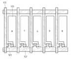
도 1은 종래 기술에 따른 액정표시장치 화소 구조를 개략적으로 도시한 평면도이다.1 is a plan view schematically illustrating a pixel structure of a liquid crystal display according to the related art.
도 1에 도시된 바와 같이, TN(Twist Nematic) 모드 또는 VA(Vertical Alignment) 모드와 같은 액정표시장치의 어레이 기판은 수직으로 교차 배열된 게이트 버스 라인(20)과 데이터 버스 라인(10)에 의해 화소 영역이 정의된다.As shown in FIG. 1, an array substrate of a liquid crystal display device, such as a twist nematic (TN) mode or a vertical alignment (VA) mode, is formed by a
상기 화소 영역 상에는 ITO 투명 금속으로 형성된 화소 전극(15)이 상기 데이터 버스 라인(10)과 평행한 방향으로 배치되어 있다.On the pixel region, a
또한, 상기 데이터 버스 라인(10)과 게이트 버스 라인(20)이 수직으로 교차 배열된 영역에는 스위칭 소자인 박막 트랜지스터(Thin Film Transistor:TFT)가 배치되어 있어, 상기 게이트 버스 라인(20)에 인가되는 구동신호에 의해 TFT가 턴온되면, 상기 데이터 버스 라인(10)에 인가된 데이터 신호가 상기 TFT의 채널층을 통하여 상기 화소 전극(15)으로 인가된다.In addition, a thin film transistor (TFT), which is a switching element, is disposed in an area where the
이렇게 상기 화소 전극(15)에 인가된 데이터 신호는 컬러필터기판 상에 형성된 공통 전극과 함께 액정분자들을 회전시키는 전계를 형성하는데, 액정분자들의 회전 정도에 따라 백라이트 유닛으로부터 발생된 광의 투과율이 조절된다. The data signal applied to the
이렇게 액정분자의 회전에 따라 투과율이 조절된 광은 컬러필터기판 상에 형성된 레드(R), 그린(G), 블루(B) 컬러필터층을 통과하면서 다양한 색상을 재현하고, 이를 이용하여 화상을 디스플레이 하게 된다.The light whose transmittance is adjusted according to the rotation of the liquid crystal molecules passes through the red (R), green (G), and blue (B) color filter layers formed on the color filter substrate, and reproduces various colors, and displays an image by using the same. Done.
상기 화소전극(15) 상에 표시된 R, G, B는 컬러필터기판 상에 형성된 레드, 그린, 블루 컬러필터층을 나타낸 것이다.R, G, and B displayed on the
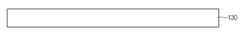
도 2는 상기 도 1의 화소구조에 대응하는 컬러필터기판을 도시한 단면도이다.FIG. 2 is a cross-sectional view illustrating a color filter substrate corresponding to the pixel structure of FIG. 1.
도 2에 도시된 바와 같이, 컬러필터기판은 투명한 하부기판(30) 상에 블랙 매트릭스(31)가 형성되어 있고, 상기 블랙 매트릭스(31) 사이에는 레드(R), 그린(G), 블루(B) 컬러필터층(35, 36, 37)이 교대로 형성되어 있다.As shown in FIG. 2, the color filter substrate has a
상기 레드(R), 그린(G), 블루(B) 컬러필터층(35, 36, 37)이 형성된 하부기판(30) 상에는 평탄화를 위하여 오버코트층(40)이 형성되어 있고, 상기 오버코트층 (40) 상에는 투명성 도전 금속으로 형성된 공통전극(42)이 형성되어 있다. 상기 블랙 매트릭스(31)는 백라이트 유닛으로부터 발생되는 광을 차단하는 차단영역에 형성되기 때문에 상기 도 1의 데이터 버스 라인, 게이트 버스 라인 및 TFT 영역과 대응되는 영역에 형성된다.On the
그러나, 상기와 같이 레드, 그린, 블루 컬러필터층으로된 3개의 서브픽셀이 하나의 단위픽셀 구조를 갖는 종래 액정표시장치는 단위픽셀당 광투과율이 낮아 저휘도 특성을 갖는 단점이 있다.However, the conventional liquid crystal display device having three unit pixels of one red, green, and blue color filter layers as described above has one unit pixel structure has a low luminance characteristic because of low light transmittance per unit pixel.
특히, 고해상도 모델의 경우에는 각각의 서브픽셀들의 크기가 작아지는데, 이럴 경우에는 고해상도 구현을 하여야함에도 불구하여 낮은 휘도 특성 때문에 화면품위가 떨어지는 문제가 발생한다.In particular, in the case of a high resolution model, the size of each subpixel is reduced. In this case, the screen quality is deteriorated due to the low luminance characteristic even though a high resolution is required.
또한, 사람의 시각을 기준으로 휘도 특성과 관련이 깊은 것은 레드, 그린, 블루 컬러중 그린 컬러이기 때문에 하나의 그린 컬러층으로만은 높은 휘도값을 얻기는 한계가 있다.In addition, since the green color of the red, green, and blue colors is deeply related to the luminance characteristic based on the human eye, there is a limit in obtaining a high luminance value using only one green color layer.
본 발명은, 레드, 그린, 블루 컬러층과 화이트 컬러층을 추가하여 단위 픽셀을 구현함으로써, 높은 휘도 특성을 얻도록한 컬러필터기판 및 그 제조방법을 제공함에 그 목적이 있다.It is an object of the present invention to provide a color filter substrate and a method of manufacturing the same, which achieve a high luminance characteristic by adding a red, green, blue color layer and a white color layer to implement unit pixels.
또한, 화이트 컬러층을 화이트 안료를 사용하여 형성하지 않고, 투명한 하부기판을 패터닝하거나 오버코트층 또는 투명한 ITO으로 형성함으로써, 화이트 컬러층의 투과율을 높여 고휘도 특성을 구현할 수 있도록 한 컬러필터기판 및 그 제조 방법을 제공함에 그 목적이 있다.In addition, without forming a white color layer using a white pigment, by forming a transparent lower substrate or by forming an overcoat layer or transparent ITO, a color filter substrate that can achieve high brightness characteristics by increasing the transmittance of the white color layer and its manufacture The purpose is to provide a method.
상기한 목적을 달성하기 위한, 본 발명에 따른 컬러필터기판은,In order to achieve the above object, the color filter substrate according to the present invention,
기판;Board;
상기 기판을 패터닝하여 형성된 화이트 컬러필터층;A white color filter layer formed by patterning the substrate;
상기 화이트 컬러필터층이 형성된 기판 상에 형성된 블랙 매트릭스; 및A black matrix formed on the substrate on which the white color filter layer is formed; And
상기 기판 상에 형성된 블랙 매트릭스 사이에 교대로 형성된 레드 컬러필터층, 그린 컬러필터층, 블루 컬러필터층을 포함한다.And a red color filter layer, a green color filter layer, and a blue color filter layer that are alternately formed between the black matrices formed on the substrate.
또한, 본 발명의 다른 실시예에 의한 컬러필터기판 제조방법은,In addition, the color filter substrate manufacturing method according to another embodiment of the present invention,
기판을 제공하는 단계;Providing a substrate;
상기 기판을 식각하여 화이트 컬러필터층을 형성하는 단계;Etching the substrate to form a white color filter layer;
상기 화이트 컬러필터층이 형성된 기판 상에 블랙 매트릭스를 형성하는 단계; 및Forming a black matrix on the substrate on which the white color filter layer is formed; And
상기 블랙 매트릭스가 형성된 기판 상에 레드 컬러필터층, 그린 컬러필터층, 블루 컬러필터층을 순차적으로 형성하는 단계를 포함한다.And sequentially forming a red color filter layer, a green color filter layer, and a blue color filter layer on the substrate on which the black matrix is formed.
본 발명의 또 다른 실시예에 의한 컬러필터기판은,The color filter substrate according to another embodiment of the present invention,
기판;Board;
상기 기판 상에 형성된 블랙 매트릭스;A black matrix formed on the substrate;
상기 기판 상에 형성된 블랙 매트릭스 사이에 교대로 형성된 레드 컬러필터층, 그린 컬러필터층, 블루 컬러필터층, 화이트 컬러필터층; 및A red color filter layer, a green color filter layer, a blue color filter layer, and a white color filter layer that are alternately formed between the black matrices formed on the substrate; And
상기 레드 컬러필터층, 그린 컬러필터층, 블루 컬러필터층 및 화이트 컬러필터층이 형성된 기판 상에 오버코트층을 포함한다.An overcoat layer is formed on the substrate on which the red color filter layer, the green color filter layer, the blue color filter layer, and the white color filter layer are formed.
본 발명의 또 다른 실시예에 의한 컬러필터기판 제조방법은,The color filter substrate manufacturing method according to another embodiment of the present invention,
기판을 제공하는 단계;Providing a substrate;
상기 기판을 상에 블랙 매트릭스를 형성하는 단계;Forming a black matrix on the substrate;
상기 블랙 매트릭스가 형성된 기판 상에 컬러레진을 사용하여 레드 컬러필터층, 그린 컬러필터층, 블루 컬러필터층을 순차적으로 형성하는 단계; 및Sequentially forming a red color filter layer, a green color filter layer, and a blue color filter layer using a color resin on the substrate on which the black matrix is formed; And
상기 레드 컬러필터층, 그린 컬러필터층, 블루 컬러필터층이 형성된 기판 상에 투명금속을 형성하고 식각하여 화이트 컬리필터층을 형성하는 단계를 포함한다.And forming a white metal filter layer by forming and etching a transparent metal on the substrate on which the red color filter layer, the green color filter layer, and the blue color filter layer are formed.
본 발명에 의하면, 레드, 그린, 블루 컬러층과 화이트 컬러층을 추가하여 단위 픽셀을 구현함으로써, 높은 휘도 특성을 얻도록 하였다.According to the present invention, a unit pixel is implemented by adding red, green, and blue color layers and a white color layer, thereby obtaining high luminance characteristics.
또한, 화이트 컬러층을 화이트 안료를 사용하여 형성하지 않고, 투명한 하부기판을 패터닝하거나 오버코트층 또는 투명한 ITO으로 형성함으로써, 화이트 컬러층의 투과율을 높여 고휘도 특성을 구현할 수 있도록 하였다.In addition, the white color layer is not formed using a white pigment, and the transparent lower substrate is patterned or formed by an overcoat layer or transparent ITO, thereby increasing the transmittance of the white color layer to implement high brightness characteristics.
이하, 첨부한 도면에 의거하여 본 발명의 실시 예를 자세히 설명하도록 한다.Hereinafter, embodiments of the present invention will be described in detail with reference to the accompanying drawings.
도 3은 본 발명에 따른 액정표시장치의 화소구조를 도시한 평면도이다.3 is a plan view illustrating a pixel structure of a liquid crystal display according to the present invention.
도 3에 도시된 바와 같이, 어레이 기판은 수직으로 교차 배열된 게이트 버스 라인(102)과 데이터 버스 라인(100)에 의해 화소 영역이 정의된다.As shown in FIG. 3, a pixel region is defined in an array substrate by
상기 화소 영역 상에는 ITO 투명 금속으로 형성된 화소 전극(105)이 상기 데 이터 버스 라인(100)과 평행한 방향으로 배치되어 있다.On the pixel region, a
또한, 상기 데이터 버스 라인(100)과 게이트 버스 라인(102)이 수직으로 교차 배열된 영역에는 스위칭 소자인 박막 트랜지스터(TFT)가 배치되어 있어, 상기 게이트 버스 라인(102)에 인가되는 구동신호에 의해 TFT가 턴온되면, 상기 데이터 버스 라인(100)에 인가된 데이터 신호가 상기 TFT의 채널층을 통하여 상기 화소 전극(105)으로 인가된다.In addition, a thin film transistor (TFT), which is a switching element, is disposed in an area where the
상기 화소전극(105) 상에 표시된 W는 컬러필터기판 상에 형성된 화이트(White) 컬러필터층, R은 레드(Red) 컬러필터층, G는 그린(Green) 컬러필터층, B는 블루(Blue) 컬러필터층을 나타낸다.W denoted on the
본 발명에서는 상기 화소전극(105)에 대응되는 컬러필터기판의 컬러필터층이 종래와 달리 레드(Red), 그린(Green), 블루(Blue), 화이트(White) 네개의 서브픽셀이 하나의 단위 픽셀 구조를 형성한다.In the present invention, unlike the conventional color filter layer of the color filter substrate corresponding to the
상기 화이트 컬러 필터층에 대응하는 화소 전극은 종래 RGB 단위픽셀 영역에 추가적으로 하나의 화이트 영역을 형성할 수 있고, RGB 서브 픽셀과 동일한 크기의 서브 픽셀을 화이트 서브 픽셀로 하여 단위픽셀을 형성할 수 있다.The pixel electrode corresponding to the white color filter layer may form one white region in addition to the conventional RGB unit pixel region, and may form a unit pixel using a subpixel having the same size as the RGB subpixel as a white subpixel.
RGBW를 하나의 단위픽셀로 형성된 경우에는 단위픽셀단위로 화상을 디스플레이한다.When RGBW is formed of one unit pixel, an image is displayed in unit pixel units.
따라서, 종래 RGB 단위픽셀 영역에 네개의 RGBW 서브 픽셀을 형성한 경우에는 화이트(W) 서브픽셀이 추가되었기 때문에 단위 픽셀당 투과율을 높아져 고휘도값을 얻을 수 있다. 마찬가지로 종래 RGB 서브 픽셀과 같은 크기의 화이트 픽셀이 추가되어 단위픽셀을 형성하는 경우에도 화이트 서브픽셀에의해 투과영역이 넓어졌기 때문에 고휘도 특성을 구현할 수 있다.Therefore, when four RGBW subpixels are formed in a conventional RGB unit pixel area, since white (W) subpixels are added, the transmittance per unit pixel may be increased to obtain a high luminance value. Similarly, when a white pixel having the same size as a conventional RGB sub pixel is added to form a unit pixel, the transmissive area is widened by the white sub pixel, thereby achieving high luminance.
도 4a 내지 도 4e는 본 발명에 따른 컬러필터기판의 제조공정을 도시한 도면이다.4A to 4E are views illustrating a manufacturing process of a color filter substrate according to the present invention.
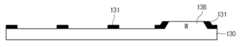
도 4a 및 도 4b에 도시한 바와 같이, 투명성 절연기판인 하부기판(130)을 제공한 다음, 이를 제 1 마스크 공정에 따라 식각하여 화이트 컬러필터층(138)을 패터닝한다.As shown in FIGS. 4A and 4B, the
이때, 최초 제공되는 하부기판(130)은 종래 컬러필터기판 제조를 위하여 제공된 기판보다 화이트 컬러필터층(138)의 두께만큼 두껍다. 이때, 상기 하부기판(130)은 보통 유리를 사용하는데, 이를 식각하기 위해서는 HF6(gas)를 이용한 건식각(Dry Etching) 방식 또는 HF(liquid)를 이용한 습식각(Wet eching) 방식을 사용한다.In this case, the first
따라서, 화이트 컬러 필터층(138)은 하부기판(130)의 재질로 되어 있기 때문에 백라이트 유닛으로부터 발생된 광이 하부기판(130)을 통과하여 화이트 컬러를 구현하기 때문에 광휘도 특성이 좋아진다.Accordingly, since the white
이와 같이 하부기판(130) 상에 화이트 컬러 필터층(138)이 형성되면, 도 4c에 도시한 바와 같이, 상기 하부기판(130)의 전 영역 상에 크롬(Cr) 또는 광차단성 수지를 형성한 다음, 제 2 마스크 공정에 따라 패터닝하여 블랙 매트릭스(131)를 형성한다.When the white
상기 블랙 매트릭스(131)는 컬러필터층이 형성될 영역을 격자형태로 구획하여 형성된다. 도면에서와 같이 화이트 컬러필터층(138) 양측 가장자리에 블랙 매트릭스(131)가 패터닝되어 있다.The
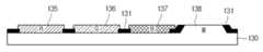
그런 다음, 도 4d에 도시한 바와 같이, 상기 블랙 매트릭스(131)가 형성된 하부기판(130) 상에 레드 컬러레진을 도포한 다음, 제 3 마스크 공정에 따라 패터닝하여 레드 컬러필터층(135)을 형성한다.Next, as shown in FIG. 4D, the red color resin is coated on the
이와 같은 방식으로 제 4 마스크 공정과 제 5 마스크 공정을 진행하여 그린 컬러 필터층(136)과 블루 컬러필터층(137)을 순차적으로 형성하여 상기 하부기판(130) 상에 레드 컬러필터층(135), 그린 컬러필터층(136), 블루 컬러필터층(137) 및 화이트 컬러필터층(138)을 형성한다.In this manner, the fourth color mask process and the fifth color mask process are performed to sequentially form the green
또한, 상기 화이트 컬러필터층(138)의 높이는 상기 레드 컬러필터층(135), 그린 컬러필터층(136), 블루 컬러필터층(137)들과 동일한 높이로 패터닝되어 있어 이후 막형성시 균일한 유니포머티를 얻을 수 있다.In addition, the height of the white
상기에서와 같이 레드 컬러필터층(135), 그린 컬러필터층(136), 블루 컬러필터층(137) 및 화이트 컬러필터층(138)이 하부기판(130) 상에 형성되면, 도 4e에 도시한 바와 같이, 하부기판(130) 상에 오버코트층(140)과 ITO 금속막으로된 공통전극(142)을 형성한다.As described above, when the red
상기 하부기판(130)을 식각하여 형성한 화이트 컬러필터층(138)의 높이는 상기 레드 컬러필터층(135), 그린 컬러필터층(136), 블루 컬러필터층(137)들과 동일한 높이로 패터닝되어 있기 때문에 상기 오버코트층(140)과 공통전극(142)은 단차 영향없이 균일하게 형성된다.The height of the white
이와 같이 공통전극(142)과 오버코트층(140)이 단차없이 균일한 유니포머티를 얻게 되면, 이후 도포되는 배향막이 균일하게 도포될 수 있어 단차에 의한 배향 불균형을 방지할 수 있다.As such, when the
상기 도면에서는 오버코트층(140)과 공통전극(142)이 형성되는 TN(Twist Nematic) 또는 VA(Vertical Alignment) 모드 액정표시장치의 컬러필터기판을 기준으로 설명하였지만, 오버코트층(140)을 형성하지 않는 모델인 경우에는 곧바로 공통전극(142)만 형성할 수 있다.Although FIG. 5 illustrates the color filter substrate of the twisted nematic (TN) or vertical alignment (VA) mode liquid crystal display in which the
또한, 상기 도면에서는 액정표시장치의 어레이 기판 상에 화소전극이 형성되어 있고, 컬러필터기판 상에 공통전극이 형성된 TN 또는 VA 모드 액정표시장치의 컬러필터기판을 기준으로 설명하였지만, 어레이 기판 상에 화소전극과 공통전극이 형성된 IPS(In-Plane Switching) 모드 또는 FFS(Fringe Field Switching) 모드 액정표시장치 컬러필터기판에도 적용할 수 있다.In the drawing, the pixel electrode is formed on the array substrate of the liquid crystal display device and the color filter substrate of the TN or VA mode liquid crystal display device in which the common electrode is formed on the color filter substrate is described. The present invention can also be applied to an IPS (In-Plane Switching) mode or a FFS (Fringe Field Switching) mode liquid crystal display color filter substrate having a pixel electrode and a common electrode.
만약, IPS 모드 또는 FFS 모드 액정표시장치 컬러필터기판 제조일 경우에는 오버코트층(140) 상에 공통전극 형성하는 공정은 생략된다.If the IPS mode or FFS mode liquid crystal display color filter substrate is manufactured, the process of forming the common electrode on the
본 발명에서는 종래 RGB 컬러필터층으로 구성된 픽셀을 RGBW 컬러필터층으로 구성된 픽셀구조로 형성함으로써, 단위 픽셀당 광투과율을 높일 수 있어 고휘도 영상을 구현할 수 있는 효과가 있다.In the present invention, by forming a pixel composed of a conventional RGB color filter layer in a pixel structure composed of an RGBW color filter layer, it is possible to increase the light transmittance per unit pixel, thereby implementing a high brightness image.
도 5 내지 도 6은 본 발명의 다른 실시예에 따른 컬러필터기판의 구조를 도시한 도면이다.5 to 6 illustrate the structure of a color filter substrate according to another exemplary embodiment of the present invention.
도 5는 화이트 컬러필터층(238)이 오버코트층(240)으로 형성된 것이고, 도 6 은 화이트 컬러필터층(338)이 투명금속으로 형성되어 있다.In FIG. 5, the white
도 5의 컬러필터기판의 제조공정과 구조를 살펴보면 다음과 같다.Looking at the manufacturing process and structure of the color filter substrate of Figure 5 as follows.
먼저, 투명성 절연기판으로된 하부기판(230) 상에 제 1 마스크 공정에 따라 블랙 매트릭스(231)를 형성하고, 이후 순차적으로 마스크 공정을 진행하여 레드 컬러필터층(235), 그린 컬러필터층(236), 블루 컬러필터층(237)을 순차적으로 형성한다.First, a
이때, 화이트 컬러필터층(238)이 형성될 영역은 상기 하부기판(230)이 노출된 상태이다.In this case, the
상기와 같이 레드 컬러필터층(235), 그린 컬러필터층(236), 블루 컬러필터층(237)이 하부기판(230) 상에 순차적으로 형성되면, 상기 하부기판(230) 전 영역 상에 오버코트층(240)을 형성한다.As described above, when the red
이때, 상기 오버코트층(240)은 레드 컬러필터층(235), 그린 컬러필터층(236), 블루 컬러필터층(237) 상부에 형성되면서, 화이트 컬러필터층(238)이 형성될 영역에 채워져 화이트 컬러필터층(238)을 형성하게 된다.In this case, the
즉, 상기 오버코트층(240)과 화이트 컬러필터층(238)은 동시에 형성되어 화이트 컬러필터층(238)을 형성하기 위한 별도의 추가 공정이 필요하지 않는 장점이 있다.That is, the
상기와 같이 오버코트층(240)이 하부기판(230) 상에 형성되면, 투명성 금속막을 형성하여 공통전극(242)을 형성한다.When the
상기 도면에서는 오버코트층(240)과 공통전극(242)이 형성되는 TN(Twist Nematic) 또는 VA(Vertical Alignment) 모드 액정표시장치의 컬러필터기판을 기준으로 설명하였지만, 오버코트층(240)을 형성하지 않는 모델인 경우에는 곧바로 공통전극(242)만 형성할 수 있다.Although FIG. 5 illustrates the color filter substrate of the TN (Twist Nematic) or VA (Vertical Alignment) mode liquid crystal display in which the
이경우에는 공통전극(242)이 화이트 컬러필터층 역할을 할 것이다.In this case, the
상기 도면에서는 액정표시장치의 어레이 기판 상에 화소전극이 형성되어 있고, 컬러필터기판 상에 공통전극이 형성된 TN(Twist Nematic) 또는 VA 모드 액정표시장치의 컬러필터기판을 기준으로 설명하였지만, 어레이 기판 상에 화소전극과 공통전극이 형성된 IPS(In-Plane Switching) 모드 또는 FFS(Fringe Field Switching) 모드 액정표시장치 컬러필터기판에도 적용할 수 있다.In the drawing, the pixel electrode is formed on the array substrate of the liquid crystal display and the color filter substrate of the TN (Twist Nematic) or VA mode liquid crystal display in which the common electrode is formed on the color filter substrate is described. The present invention can also be applied to IPS (In-Plane Switching) mode or FFS (Fringe Field Switching) mode liquid crystal display color filter substrate having a pixel electrode and a common electrode formed thereon.
만약, IPS 모드 또는 FFS 모드 액정표시장치 컬러필터기판 제조일 경우에는 오버코트층(240) 상에 공통전극 형성하는 공정은 생략된다.If the IPS mode or FFS mode liquid crystal display color filter substrate is manufactured, the process of forming the common electrode on the
본 발명에서는 종래 RGB 컬러필터층으로 구성된 픽셀을 RGBW 컬러필터층으로 구성된 픽셀구조로 형성함으로써, 단위 픽셀당 광투과율을 높일 수 있어 고휘도 영상을 구현할 수 있는 효과가 있다.In the present invention, by forming a pixel composed of a conventional RGB color filter layer in a pixel structure composed of an RGBW color filter layer, it is possible to increase the light transmittance per unit pixel, thereby implementing a high brightness image.
본 발명에서는 종래 RGB 컬러필터층으로 구성된 픽셀을 RGBW 컬러필터층으로 구성된 픽셀구조로 형성함으로써, 단위 픽셀당 광투과율을 높일 수 있어 고휘도 영상을 구현할 수 있는 효과가 있다.In the present invention, by forming a pixel composed of a conventional RGB color filter layer in a pixel structure composed of an RGBW color filter layer, it is possible to increase the light transmittance per unit pixel, thereby implementing a high brightness image.
도 6의 컬러필터기판 제조공정과 구조를 살펴보면 다음과 같다.Looking at the manufacturing process and structure of the color filter substrate of Figure 6 as follows.
먼저, 투명성 절연기판으로된 하부기판(330) 상에 제 1 마스크 공정에 따라 블랙 매트릭스(331)를 형성하고, 이후 순차적으로 마스크 공정을 진행하여 레드 컬 러필터층(335), 그린 컬러필터층(336), 블루 컬러필터층(337)을 순차적으로 형성한다.First, the
그런 다음 상기 하부기판(330) 상에 ITO, IZO 투명 금속을 형성한 다음, 이를 식각하여 화이트 컬러필터층(338)을 형성한다. 즉, RGBW 컬러필터층을 형성하기 위해 각각의 마스크 공정을 진행하여 컬러필터층을 형성한다.Thereafter, ITO and IZO transparent metals are formed on the
상기와 같이 하부기판(330) 상에 레드 컬러필터층(335), 그린 컬러필터층(336), 블루 컬러필터층(337) 및 화이트 컬러필터층(338)이 형성되면, 오버코트층(340)을 상기 하부기판(330) 상에 형성한다.As described above, when the red
그리고, 투명성 금속(ITO, IZO)를 사용하여 공통전극(342)을 형성한다.The
상기 화이트 컬러필터층(338)은 투명 금속으로 형성할 수 있고, 경우에 따라서는 투명컬러 레진을 사용하여 형성할 수 있다.The white
상기 도면에서는 액정표시장치의 어레이 기판 상에 화소전극이 형성되어 있고, 컬러필터기판 상에 공통전극이 형성된 TN(Twist Nematic) 또는 VA 모드 액정표시장치의 컬러필터기판을 기준으로 설명하였지만, 어레이 기판 상에 화소전극과 공통전극이 형성된 IPS(In-Plane Switching) 모드 또는 FFS(Fringe Field Switching) 모드 액정표시장치 컬러필터기판에도 적용할 수 있다.In the drawing, the pixel electrode is formed on the array substrate of the liquid crystal display and the color filter substrate of the TN (Twist Nematic) or VA mode liquid crystal display in which the common electrode is formed on the color filter substrate is described. The present invention can also be applied to IPS (In-Plane Switching) mode or FFS (Fringe Field Switching) mode liquid crystal display color filter substrate having a pixel electrode and a common electrode formed thereon.
만약, IPS 모드 또는 FFS 모드 액정표시장치 컬러필터기판 제조일 경우에는 오버코트층(240) 상에 공통전극 형성하는 공정은 생략된다.If the IPS mode or FFS mode liquid crystal display color filter substrate is manufactured, the process of forming the common electrode on the
본 발명에서는 레드 컬러필터층(335), 그린 컬러필터층(336), 블루 컬러필터층(337) 및 화이트 컬러필터층(338)이 동일한 높이로 형성되기 때문에 오버코트층 (340), 공통전극(342)이 단차없이 균일하게 형성된다.In the present invention, since the red
그래서 액정 배향을 위해서 형성하는 배향막이 균일하게 도포될 수 있어 액정 배향 불량에 따른 빛샘 불량등이 발생되지 않는다.Thus, an alignment film formed for liquid crystal alignment may be uniformly applied, so that light leakage defects due to liquid crystal alignment defects do not occur.
또한, 본 발명에서는 종래 RGB 컬러필터층으로 구성된 픽셀을 RGBW 컬러필터층으로 구성된 픽셀구조로 형성함으로써, 단위 픽셀당 광투과율을 높일 수 있어 고휘도 영상을 구현할 수 있는 효과가 있다.In addition, in the present invention, by forming a pixel composed of a conventional RGB color filter layer in a pixel structure composed of an RGBW color filter layer, it is possible to increase the light transmittance per pixel, thereby realizing a high brightness image.
이상에서 자세히 설명된 바와 같이, 본 발명은 종래 RGB 컬러필터층을 RGBW 컬러필터층으로 형성하여 단위 픽셀당 투과율을 향상시켜 고휘도 액정표시장치를 구현할 수 있는 효과가 있다.As described in detail above, the present invention has the effect of implementing a high luminance liquid crystal display device by forming a conventional RGB color filter layer as an RGBW color filter layer to improve transmittance per unit pixel.
또한, 화이트 컬러필터층을 투명성 절연기판, 투명금속, 오버코트층, 투명컬러레진등으로 형성하여 균일한 배향막을 형성할 수 있는 효과가 있다.In addition, the white color filter layer may be formed of a transparent insulating substrate, a transparent metal, an overcoat layer, a transparent color resin, or the like to form a uniform alignment layer.
또한, 화이트 컬러필터층을 투명성 절연기판 또는 오버코트층으로 형성할 경우에는 백라이트 유닛으로 부터 발생된 광의 투과율이 높아져 고휘도 특성의 컬러필터기판을 구현할 수 있는 효과가 있다.In addition, when the white color filter layer is formed of a transparent insulating substrate or an overcoat layer, the transmittance of light generated from the backlight unit is increased, thereby achieving a color filter substrate having a high luminance characteristic.
본 발명은 상기한 실시 예에 한정되지 않고, 이하 청구 범위에서 청구하는 본 발명의 요지를 벗어남이 없이 당해 발명이 속하는 분야에서 통상의 지식을 가진 자라면 누구든지 다양한 변경 실시가 가능할 것이다.It will be understood by those skilled in the art that various changes in form and details may be made therein without departing from the spirit and scope of the invention as defined by the appended claims.
Claims (24)
Translated fromKoreanPriority Applications (1)
| Application Number | Priority Date | Filing Date | Title |
|---|---|---|---|
| KR1020050115251AKR101321172B1 (en) | 2005-11-30 | 2005-11-30 | Color filter substrate and method for manufacturing thereof |
Applications Claiming Priority (1)
| Application Number | Priority Date | Filing Date | Title |
|---|---|---|---|
| KR1020050115251AKR101321172B1 (en) | 2005-11-30 | 2005-11-30 | Color filter substrate and method for manufacturing thereof |
Publications (2)
| Publication Number | Publication Date |
|---|---|
| KR20070056509A KR20070056509A (en) | 2007-06-04 |
| KR101321172B1true KR101321172B1 (en) | 2013-10-22 |
Family
ID=38354256
Family Applications (1)
| Application Number | Title | Priority Date | Filing Date |
|---|---|---|---|
| KR1020050115251AExpired - Fee RelatedKR101321172B1 (en) | 2005-11-30 | 2005-11-30 | Color filter substrate and method for manufacturing thereof |
Country Status (1)
| Country | Link |
|---|---|
| KR (1) | KR101321172B1 (en) |
Cited By (2)
| Publication number | Priority date | Publication date | Assignee | Title |
|---|---|---|---|---|
| CN104503134A (en)* | 2015-01-21 | 2015-04-08 | 合肥鑫晟光电科技有限公司 | Colored film base plate, liquid crystal display panel and display device |
| US11036101B2 (en) | 2018-07-10 | 2021-06-15 | Samsung Display Co., Ltd. | Display device and manufacturing method thereof |
Families Citing this family (5)
| Publication number | Priority date | Publication date | Assignee | Title |
|---|---|---|---|---|
| KR101608870B1 (en) | 2009-02-02 | 2016-04-05 | 삼성디스플레이 주식회사 | Organic Light Emitting Display device |
| KR101698544B1 (en)* | 2009-12-02 | 2017-01-23 | 엘지디스플레이 주식회사 | Liquid crystal display module |
| TW201738586A (en)* | 2016-04-18 | 2017-11-01 | 友達光電股份有限公司 | Matrix and driving method thereof |
| CN106444144A (en)* | 2016-12-28 | 2017-02-22 | 武汉华星光电技术有限公司 | CF (color filter) substrate and display panel |
| CN106483707B (en)* | 2016-12-30 | 2019-11-01 | 东旭(昆山)显示材料有限公司 | Colour filter for liquid crystal display and preparation method thereof and liquid crystal display |
Citations (2)
| Publication number | Priority date | Publication date | Assignee | Title |
|---|---|---|---|---|
| KR19990041468A (en)* | 1997-11-21 | 1999-06-15 | 구자홍 | Color filter substrate and its manufacturing method |
| KR20050064370A (en)* | 2003-12-23 | 2005-06-29 | 엘지.필립스 엘시디 주식회사 | Liquid crystal display device and manufacturing of the same |
- 2005
- 2005-11-30KRKR1020050115251Apatent/KR101321172B1/ennot_activeExpired - Fee Related
Patent Citations (2)
| Publication number | Priority date | Publication date | Assignee | Title |
|---|---|---|---|---|
| KR19990041468A (en)* | 1997-11-21 | 1999-06-15 | 구자홍 | Color filter substrate and its manufacturing method |
| KR20050064370A (en)* | 2003-12-23 | 2005-06-29 | 엘지.필립스 엘시디 주식회사 | Liquid crystal display device and manufacturing of the same |
Cited By (2)
| Publication number | Priority date | Publication date | Assignee | Title |
|---|---|---|---|---|
| CN104503134A (en)* | 2015-01-21 | 2015-04-08 | 合肥鑫晟光电科技有限公司 | Colored film base plate, liquid crystal display panel and display device |
| US11036101B2 (en) | 2018-07-10 | 2021-06-15 | Samsung Display Co., Ltd. | Display device and manufacturing method thereof |
Also Published As
| Publication number | Publication date |
|---|---|
| KR20070056509A (en) | 2007-06-04 |
Similar Documents
| Publication | Publication Date | Title |
|---|---|---|
| JP6105602B2 (en) | Array substrate for display device, color filter substrate, and manufacturing method thereof | |
| CN100365483C (en) | Color filter array substrate and manufacturing method thereof | |
| US8026999B2 (en) | Substrate of a liquid crystal display panel, liquid crystal panel and manufacturing method thereof | |
| KR101269006B1 (en) | Liquid ctystal display device | |
| KR100643039B1 (en) | Transverse electric field type liquid crystal display device | |
| KR20050107900A (en) | In plane switching mode liquid crystal display device having improved contrast ratio | |
| CN103197462A (en) | Color film substrate, display panel and display device | |
| JP2012242497A (en) | Liquid crystal display | |
| JP6548015B2 (en) | Liquid crystal display | |
| KR20010053977A (en) | Liquid crystal displays having wide viewing angle and panels for the same | |
| WO2017186095A1 (en) | Display panel and manufacturing method thereof, and display device | |
| US20060028604A1 (en) | Liquid crystal display device | |
| KR20100046826A (en) | Viewing angle controllable liquid crystal display device | |
| WO2021196282A1 (en) | Liquid crystal display panel and manufacturing method therefor | |
| KR101321172B1 (en) | Color filter substrate and method for manufacturing thereof | |
| US8675156B2 (en) | Color filter substrate for liquid crystal display, and manufacturing method thereof | |
| US20070085956A1 (en) | Multi-domain vertical alignment thin film transistor liquid crystal display, color filter substrate and polarizer film applied thereto, and fabricating method thereof | |
| KR100698059B1 (en) | LCD and its manufacturing method | |
| WO2018045614A1 (en) | Color filter substrate, liquid crystal panel and liquid crystal display | |
| KR101719815B1 (en) | Color filter array substrate of Liquid Crysral Display Device | |
| KR100630878B1 (en) | Fringe Field Switching Mode Liquid Crystal Display Device and Method for Manufacturing the same | |
| US20070058112A1 (en) | Liquid crystal display panel, color filter, and manufacturing method thereof | |
| KR101010403B1 (en) | Liquid crystal display device with minimum cell gap variation and manufacturing method thereof | |
| KR20040103275A (en) | In-Plane Switching Mode Liquid Crystal Display device and method for fabricating the same | |
| US8576364B2 (en) | Method for forming multiple alignment films on a substrate and pixel structure of a liquid crystal display |
Legal Events
| Date | Code | Title | Description |
|---|---|---|---|
| PA0109 | Patent application | St.27 status event code:A-0-1-A10-A12-nap-PA0109 | |
| PG1501 | Laying open of application | St.27 status event code:A-1-1-Q10-Q12-nap-PG1501 | |
| PN2301 | Change of applicant | St.27 status event code:A-3-3-R10-R13-asn-PN2301 St.27 status event code:A-3-3-R10-R11-asn-PN2301 | |
| A201 | Request for examination | ||
| PA0201 | Request for examination | St.27 status event code:A-1-2-D10-D11-exm-PA0201 | |
| R18-X000 | Changes to party contact information recorded | St.27 status event code:A-3-3-R10-R18-oth-X000 | |
| R18-X000 | Changes to party contact information recorded | St.27 status event code:A-3-3-R10-R18-oth-X000 | |
| R18-X000 | Changes to party contact information recorded | St.27 status event code:A-3-3-R10-R18-oth-X000 | |
| D13-X000 | Search requested | St.27 status event code:A-1-2-D10-D13-srh-X000 | |
| D14-X000 | Search report completed | St.27 status event code:A-1-2-D10-D14-srh-X000 | |
| PE0902 | Notice of grounds for rejection | St.27 status event code:A-1-2-D10-D21-exm-PE0902 | |
| AMND | Amendment | ||
| E13-X000 | Pre-grant limitation requested | St.27 status event code:A-2-3-E10-E13-lim-X000 | |
| P11-X000 | Amendment of application requested | St.27 status event code:A-2-2-P10-P11-nap-X000 | |
| P13-X000 | Application amended | St.27 status event code:A-2-2-P10-P13-nap-X000 | |
| R17-X000 | Change to representative recorded | St.27 status event code:A-3-3-R10-R17-oth-X000 | |
| PE0902 | Notice of grounds for rejection | St.27 status event code:A-1-2-D10-D21-exm-PE0902 | |
| AMND | Amendment | ||
| P11-X000 | Amendment of application requested | St.27 status event code:A-2-2-P10-P11-nap-X000 | |
| P13-X000 | Application amended | St.27 status event code:A-2-2-P10-P13-nap-X000 | |
| E601 | Decision to refuse application | ||
| PE0601 | Decision on rejection of patent | St.27 status event code:N-2-6-B10-B15-exm-PE0601 | |
| AMND | Amendment | ||
| E13-X000 | Pre-grant limitation requested | St.27 status event code:A-2-3-E10-E13-lim-X000 | |
| J201 | Request for trial against refusal decision | ||
| P11-X000 | Amendment of application requested | St.27 status event code:A-2-2-P10-P11-nap-X000 | |
| P13-X000 | Application amended | St.27 status event code:A-2-2-P10-P13-nap-X000 | |
| PJ0201 | Trial against decision of rejection | St.27 status event code:A-3-3-V10-V11-apl-PJ0201 | |
| PB0901 | Examination by re-examination before a trial | St.27 status event code:A-6-3-E10-E12-rex-PB0901 | |
| B701 | Decision to grant | ||
| PB0701 | Decision of registration after re-examination before a trial | St.27 status event code:A-3-4-F10-F13-rex-PB0701 | |
| GRNT | Written decision to grant | ||
| PR0701 | Registration of establishment | St.27 status event code:A-2-4-F10-F11-exm-PR0701 | |
| PR1002 | Payment of registration fee | St.27 status event code:A-2-2-U10-U11-oth-PR1002 Fee payment year number:1 | |
| PG1601 | Publication of registration | St.27 status event code:A-4-4-Q10-Q13-nap-PG1601 | |
| PR1001 | Payment of annual fee | St.27 status event code:A-4-4-U10-U11-oth-PR1001 Fee payment year number:4 | |
| P22-X000 | Classification modified | St.27 status event code:A-4-4-P10-P22-nap-X000 | |
| PR1001 | Payment of annual fee | St.27 status event code:A-4-4-U10-U11-oth-PR1001 Fee payment year number:5 | |
| FPAY | Annual fee payment | Payment date:20180917 Year of fee payment:6 | |
| PR1001 | Payment of annual fee | St.27 status event code:A-4-4-U10-U11-oth-PR1001 Fee payment year number:6 | |
| FPAY | Annual fee payment | Payment date:20190917 Year of fee payment:7 | |
| PR1001 | Payment of annual fee | St.27 status event code:A-4-4-U10-U11-oth-PR1001 Fee payment year number:7 | |
| PR1001 | Payment of annual fee | St.27 status event code:A-4-4-U10-U11-oth-PR1001 Fee payment year number:8 | |
| PR1001 | Payment of annual fee | St.27 status event code:A-4-4-U10-U11-oth-PR1001 Fee payment year number:9 | |
| PC1903 | Unpaid annual fee | St.27 status event code:A-4-4-U10-U13-oth-PC1903 Not in force date:20221017 Payment event data comment text:Termination Category : DEFAULT_OF_REGISTRATION_FEE | |
| PC1903 | Unpaid annual fee | St.27 status event code:N-4-6-H10-H13-oth-PC1903 Ip right cessation event data comment text:Termination Category : DEFAULT_OF_REGISTRATION_FEE Not in force date:20221017 |