KR101319701B1 - Wafer Backside Interconnect Structure Connected To TSVs - Google Patents
Wafer Backside Interconnect Structure Connected To TSVsDownload PDFInfo
- Publication number
- KR101319701B1 KR101319701B1KR1020100080460AKR20100080460AKR101319701B1KR 101319701 B1KR101319701 B1KR 101319701B1KR 1020100080460 AKR1020100080460 AKR 1020100080460AKR 20100080460 AKR20100080460 AKR 20100080460AKR 101319701 B1KR101319701 B1KR 101319701B1
- Authority
- KR
- South Korea
- Prior art keywords
- metal
- semiconductor substrate
- conductive via
- tsv
- substrate
- Prior art date
- Legal status (The legal status is an assumption and is not a legal conclusion. Google has not performed a legal analysis and makes no representation as to the accuracy of the status listed.)
- Active
Links
Images


Classifications
- H—ELECTRICITY
- H01—ELECTRIC ELEMENTS
- H01L—SEMICONDUCTOR DEVICES NOT COVERED BY CLASS H10
- H01L23/00—Details of semiconductor or other solid state devices
- H01L23/48—Arrangements for conducting electric current to or from the solid state body in operation, e.g. leads, terminal arrangements ; Selection of materials therefor
- H01L23/481—Internal lead connections, e.g. via connections, feedthrough structures
- H—ELECTRICITY
- H01—ELECTRIC ELEMENTS
- H01L—SEMICONDUCTOR DEVICES NOT COVERED BY CLASS H10
- H01L24/00—Arrangements for connecting or disconnecting semiconductor or solid-state bodies; Methods or apparatus related thereto
- H01L24/80—Methods for connecting semiconductor or other solid state bodies using means for bonding being attached to, or being formed on, the surface to be connected
- H01L24/81—Methods for connecting semiconductor or other solid state bodies using means for bonding being attached to, or being formed on, the surface to be connected using a bump connector
- H—ELECTRICITY
- H01—ELECTRIC ELEMENTS
- H01L—SEMICONDUCTOR DEVICES NOT COVERED BY CLASS H10
- H01L21/00—Processes or apparatus adapted for the manufacture or treatment of semiconductor or solid state devices or of parts thereof
- H01L21/70—Manufacture or treatment of devices consisting of a plurality of solid state components formed in or on a common substrate or of parts thereof; Manufacture of integrated circuit devices or of parts thereof
- H01L21/71—Manufacture of specific parts of devices defined in group H01L21/70
- H01L21/768—Applying interconnections to be used for carrying current between separate components within a device comprising conductors and dielectrics
- H01L21/76801—Applying interconnections to be used for carrying current between separate components within a device comprising conductors and dielectrics characterised by the formation and the after-treatment of the dielectrics, e.g. smoothing
- H01L21/76802—Applying interconnections to be used for carrying current between separate components within a device comprising conductors and dielectrics characterised by the formation and the after-treatment of the dielectrics, e.g. smoothing by forming openings in dielectrics
- H01L21/76807—Applying interconnections to be used for carrying current between separate components within a device comprising conductors and dielectrics characterised by the formation and the after-treatment of the dielectrics, e.g. smoothing by forming openings in dielectrics for dual damascene structures
- H01L21/76813—Applying interconnections to be used for carrying current between separate components within a device comprising conductors and dielectrics characterised by the formation and the after-treatment of the dielectrics, e.g. smoothing by forming openings in dielectrics for dual damascene structures involving a partial via etch
- H—ELECTRICITY
- H01—ELECTRIC ELEMENTS
- H01L—SEMICONDUCTOR DEVICES NOT COVERED BY CLASS H10
- H01L21/00—Processes or apparatus adapted for the manufacture or treatment of semiconductor or solid state devices or of parts thereof
- H01L21/70—Manufacture or treatment of devices consisting of a plurality of solid state components formed in or on a common substrate or of parts thereof; Manufacture of integrated circuit devices or of parts thereof
- H01L21/71—Manufacture of specific parts of devices defined in group H01L21/70
- H01L21/768—Applying interconnections to be used for carrying current between separate components within a device comprising conductors and dielectrics
- H01L21/76801—Applying interconnections to be used for carrying current between separate components within a device comprising conductors and dielectrics characterised by the formation and the after-treatment of the dielectrics, e.g. smoothing
- H01L21/76802—Applying interconnections to be used for carrying current between separate components within a device comprising conductors and dielectrics characterised by the formation and the after-treatment of the dielectrics, e.g. smoothing by forming openings in dielectrics
- H01L21/76816—Aspects relating to the layout of the pattern or to the size of vias or trenches
- H—ELECTRICITY
- H01—ELECTRIC ELEMENTS
- H01L—SEMICONDUCTOR DEVICES NOT COVERED BY CLASS H10
- H01L21/00—Processes or apparatus adapted for the manufacture or treatment of semiconductor or solid state devices or of parts thereof
- H01L21/70—Manufacture or treatment of devices consisting of a plurality of solid state components formed in or on a common substrate or of parts thereof; Manufacture of integrated circuit devices or of parts thereof
- H01L21/71—Manufacture of specific parts of devices defined in group H01L21/70
- H01L21/768—Applying interconnections to be used for carrying current between separate components within a device comprising conductors and dielectrics
- H01L21/76838—Applying interconnections to be used for carrying current between separate components within a device comprising conductors and dielectrics characterised by the formation and the after-treatment of the conductors
- H01L21/76841—Barrier, adhesion or liner layers
- H01L21/76843—Barrier, adhesion or liner layers formed in openings in a dielectric
- H—ELECTRICITY
- H01—ELECTRIC ELEMENTS
- H01L—SEMICONDUCTOR DEVICES NOT COVERED BY CLASS H10
- H01L21/00—Processes or apparatus adapted for the manufacture or treatment of semiconductor or solid state devices or of parts thereof
- H01L21/70—Manufacture or treatment of devices consisting of a plurality of solid state components formed in or on a common substrate or of parts thereof; Manufacture of integrated circuit devices or of parts thereof
- H01L21/71—Manufacture of specific parts of devices defined in group H01L21/70
- H01L21/768—Applying interconnections to be used for carrying current between separate components within a device comprising conductors and dielectrics
- H01L21/76838—Applying interconnections to be used for carrying current between separate components within a device comprising conductors and dielectrics characterised by the formation and the after-treatment of the conductors
- H01L21/76877—Filling of holes, grooves or trenches, e.g. vias, with conductive material
- H—ELECTRICITY
- H01—ELECTRIC ELEMENTS
- H01L—SEMICONDUCTOR DEVICES NOT COVERED BY CLASS H10
- H01L21/00—Processes or apparatus adapted for the manufacture or treatment of semiconductor or solid state devices or of parts thereof
- H01L21/70—Manufacture or treatment of devices consisting of a plurality of solid state components formed in or on a common substrate or of parts thereof; Manufacture of integrated circuit devices or of parts thereof
- H01L21/71—Manufacture of specific parts of devices defined in group H01L21/70
- H01L21/768—Applying interconnections to be used for carrying current between separate components within a device comprising conductors and dielectrics
- H01L21/76898—Applying interconnections to be used for carrying current between separate components within a device comprising conductors and dielectrics formed through a semiconductor substrate
- H—ELECTRICITY
- H01—ELECTRIC ELEMENTS
- H01L—SEMICONDUCTOR DEVICES NOT COVERED BY CLASS H10
- H01L24/00—Arrangements for connecting or disconnecting semiconductor or solid-state bodies; Methods or apparatus related thereto
- H01L24/01—Means for bonding being attached to, or being formed on, the surface to be connected, e.g. chip-to-package, die-attach, "first-level" interconnects; Manufacturing methods related thereto
- H01L24/02—Bonding areas ; Manufacturing methods related thereto
- H01L24/03—Manufacturing methods
- H—ELECTRICITY
- H01—ELECTRIC ELEMENTS
- H01L—SEMICONDUCTOR DEVICES NOT COVERED BY CLASS H10
- H01L24/00—Arrangements for connecting or disconnecting semiconductor or solid-state bodies; Methods or apparatus related thereto
- H01L24/01—Means for bonding being attached to, or being formed on, the surface to be connected, e.g. chip-to-package, die-attach, "first-level" interconnects; Manufacturing methods related thereto
- H01L24/02—Bonding areas ; Manufacturing methods related thereto
- H01L24/04—Structure, shape, material or disposition of the bonding areas prior to the connecting process
- H01L24/05—Structure, shape, material or disposition of the bonding areas prior to the connecting process of an individual bonding area
- H—ELECTRICITY
- H01—ELECTRIC ELEMENTS
- H01L—SEMICONDUCTOR DEVICES NOT COVERED BY CLASS H10
- H01L24/00—Arrangements for connecting or disconnecting semiconductor or solid-state bodies; Methods or apparatus related thereto
- H01L24/01—Means for bonding being attached to, or being formed on, the surface to be connected, e.g. chip-to-package, die-attach, "first-level" interconnects; Manufacturing methods related thereto
- H01L24/10—Bump connectors ; Manufacturing methods related thereto
- H01L24/11—Manufacturing methods
- H—ELECTRICITY
- H01—ELECTRIC ELEMENTS
- H01L—SEMICONDUCTOR DEVICES NOT COVERED BY CLASS H10
- H01L24/00—Arrangements for connecting or disconnecting semiconductor or solid-state bodies; Methods or apparatus related thereto
- H01L24/01—Means for bonding being attached to, or being formed on, the surface to be connected, e.g. chip-to-package, die-attach, "first-level" interconnects; Manufacturing methods related thereto
- H01L24/10—Bump connectors ; Manufacturing methods related thereto
- H01L24/12—Structure, shape, material or disposition of the bump connectors prior to the connecting process
- H01L24/13—Structure, shape, material or disposition of the bump connectors prior to the connecting process of an individual bump connector
- H—ELECTRICITY
- H01—ELECTRIC ELEMENTS
- H01L—SEMICONDUCTOR DEVICES NOT COVERED BY CLASS H10
- H01L24/00—Arrangements for connecting or disconnecting semiconductor or solid-state bodies; Methods or apparatus related thereto
- H01L24/01—Means for bonding being attached to, or being formed on, the surface to be connected, e.g. chip-to-package, die-attach, "first-level" interconnects; Manufacturing methods related thereto
- H01L24/10—Bump connectors ; Manufacturing methods related thereto
- H01L24/12—Structure, shape, material or disposition of the bump connectors prior to the connecting process
- H01L24/14—Structure, shape, material or disposition of the bump connectors prior to the connecting process of a plurality of bump connectors
- H—ELECTRICITY
- H01—ELECTRIC ELEMENTS
- H01L—SEMICONDUCTOR DEVICES NOT COVERED BY CLASS H10
- H01L2224/00—Indexing scheme for arrangements for connecting or disconnecting semiconductor or solid-state bodies and methods related thereto as covered by H01L24/00
- H01L2224/01—Means for bonding being attached to, or being formed on, the surface to be connected, e.g. chip-to-package, die-attach, "first-level" interconnects; Manufacturing methods related thereto
- H01L2224/02—Bonding areas; Manufacturing methods related thereto
- H01L2224/04—Structure, shape, material or disposition of the bonding areas prior to the connecting process
- H01L2224/0401—Bonding areas specifically adapted for bump connectors, e.g. under bump metallisation [UBM]
- H—ELECTRICITY
- H01—ELECTRIC ELEMENTS
- H01L—SEMICONDUCTOR DEVICES NOT COVERED BY CLASS H10
- H01L2224/00—Indexing scheme for arrangements for connecting or disconnecting semiconductor or solid-state bodies and methods related thereto as covered by H01L24/00
- H01L2224/01—Means for bonding being attached to, or being formed on, the surface to be connected, e.g. chip-to-package, die-attach, "first-level" interconnects; Manufacturing methods related thereto
- H01L2224/02—Bonding areas; Manufacturing methods related thereto
- H01L2224/04—Structure, shape, material or disposition of the bonding areas prior to the connecting process
- H01L2224/05—Structure, shape, material or disposition of the bonding areas prior to the connecting process of an individual bonding area
- H01L2224/05001—Internal layers
- H01L2224/0502—Disposition
- H01L2224/05022—Disposition the internal layer being at least partially embedded in the surface
- H—ELECTRICITY
- H01—ELECTRIC ELEMENTS
- H01L—SEMICONDUCTOR DEVICES NOT COVERED BY CLASS H10
- H01L2224/00—Indexing scheme for arrangements for connecting or disconnecting semiconductor or solid-state bodies and methods related thereto as covered by H01L24/00
- H01L2224/01—Means for bonding being attached to, or being formed on, the surface to be connected, e.g. chip-to-package, die-attach, "first-level" interconnects; Manufacturing methods related thereto
- H01L2224/02—Bonding areas; Manufacturing methods related thereto
- H01L2224/04—Structure, shape, material or disposition of the bonding areas prior to the connecting process
- H01L2224/05—Structure, shape, material or disposition of the bonding areas prior to the connecting process of an individual bonding area
- H01L2224/05001—Internal layers
- H01L2224/0502—Disposition
- H01L2224/05025—Disposition the internal layer being disposed on a via connection of the semiconductor or solid-state body
- H—ELECTRICITY
- H01—ELECTRIC ELEMENTS
- H01L—SEMICONDUCTOR DEVICES NOT COVERED BY CLASS H10
- H01L2224/00—Indexing scheme for arrangements for connecting or disconnecting semiconductor or solid-state bodies and methods related thereto as covered by H01L24/00
- H01L2224/01—Means for bonding being attached to, or being formed on, the surface to be connected, e.g. chip-to-package, die-attach, "first-level" interconnects; Manufacturing methods related thereto
- H01L2224/02—Bonding areas; Manufacturing methods related thereto
- H01L2224/04—Structure, shape, material or disposition of the bonding areas prior to the connecting process
- H01L2224/05—Structure, shape, material or disposition of the bonding areas prior to the connecting process of an individual bonding area
- H01L2224/0554—External layer
- H01L2224/05541—Structure
- H01L2224/05546—Dual damascene structure
- H—ELECTRICITY
- H01—ELECTRIC ELEMENTS
- H01L—SEMICONDUCTOR DEVICES NOT COVERED BY CLASS H10
- H01L2224/00—Indexing scheme for arrangements for connecting or disconnecting semiconductor or solid-state bodies and methods related thereto as covered by H01L24/00
- H01L2224/01—Means for bonding being attached to, or being formed on, the surface to be connected, e.g. chip-to-package, die-attach, "first-level" interconnects; Manufacturing methods related thereto
- H01L2224/02—Bonding areas; Manufacturing methods related thereto
- H01L2224/04—Structure, shape, material or disposition of the bonding areas prior to the connecting process
- H01L2224/05—Structure, shape, material or disposition of the bonding areas prior to the connecting process of an individual bonding area
- H01L2224/0554—External layer
- H01L2224/05541—Structure
- H01L2224/05547—Structure comprising a core and a coating
- H—ELECTRICITY
- H01—ELECTRIC ELEMENTS
- H01L—SEMICONDUCTOR DEVICES NOT COVERED BY CLASS H10
- H01L2224/00—Indexing scheme for arrangements for connecting or disconnecting semiconductor or solid-state bodies and methods related thereto as covered by H01L24/00
- H01L2224/01—Means for bonding being attached to, or being formed on, the surface to be connected, e.g. chip-to-package, die-attach, "first-level" interconnects; Manufacturing methods related thereto
- H01L2224/02—Bonding areas; Manufacturing methods related thereto
- H01L2224/04—Structure, shape, material or disposition of the bonding areas prior to the connecting process
- H01L2224/05—Structure, shape, material or disposition of the bonding areas prior to the connecting process of an individual bonding area
- H01L2224/0554—External layer
- H01L2224/0556—Disposition
- H01L2224/05567—Disposition the external layer being at least partially embedded in the surface
- H—ELECTRICITY
- H01—ELECTRIC ELEMENTS
- H01L—SEMICONDUCTOR DEVICES NOT COVERED BY CLASS H10
- H01L2224/00—Indexing scheme for arrangements for connecting or disconnecting semiconductor or solid-state bodies and methods related thereto as covered by H01L24/00
- H01L2224/01—Means for bonding being attached to, or being formed on, the surface to be connected, e.g. chip-to-package, die-attach, "first-level" interconnects; Manufacturing methods related thereto
- H01L2224/02—Bonding areas; Manufacturing methods related thereto
- H01L2224/04—Structure, shape, material or disposition of the bonding areas prior to the connecting process
- H01L2224/05—Structure, shape, material or disposition of the bonding areas prior to the connecting process of an individual bonding area
- H01L2224/0554—External layer
- H01L2224/0556—Disposition
- H01L2224/0557—Disposition the external layer being disposed on a via connection of the semiconductor or solid-state body
- H—ELECTRICITY
- H01—ELECTRIC ELEMENTS
- H01L—SEMICONDUCTOR DEVICES NOT COVERED BY CLASS H10
- H01L2224/00—Indexing scheme for arrangements for connecting or disconnecting semiconductor or solid-state bodies and methods related thereto as covered by H01L24/00
- H01L2224/01—Means for bonding being attached to, or being formed on, the surface to be connected, e.g. chip-to-package, die-attach, "first-level" interconnects; Manufacturing methods related thereto
- H01L2224/02—Bonding areas; Manufacturing methods related thereto
- H01L2224/04—Structure, shape, material or disposition of the bonding areas prior to the connecting process
- H01L2224/05—Structure, shape, material or disposition of the bonding areas prior to the connecting process of an individual bonding area
- H01L2224/0554—External layer
- H01L2224/0556—Disposition
- H01L2224/05571—Disposition the external layer being disposed in a recess of the surface
- H—ELECTRICITY
- H01—ELECTRIC ELEMENTS
- H01L—SEMICONDUCTOR DEVICES NOT COVERED BY CLASS H10
- H01L2224/00—Indexing scheme for arrangements for connecting or disconnecting semiconductor or solid-state bodies and methods related thereto as covered by H01L24/00
- H01L2224/01—Means for bonding being attached to, or being formed on, the surface to be connected, e.g. chip-to-package, die-attach, "first-level" interconnects; Manufacturing methods related thereto
- H01L2224/02—Bonding areas; Manufacturing methods related thereto
- H01L2224/04—Structure, shape, material or disposition of the bonding areas prior to the connecting process
- H01L2224/06—Structure, shape, material or disposition of the bonding areas prior to the connecting process of a plurality of bonding areas
- H01L2224/061—Disposition
- H01L2224/0618—Disposition being disposed on at least two different sides of the body, e.g. dual array
- H01L2224/06181—On opposite sides of the body
- H—ELECTRICITY
- H01—ELECTRIC ELEMENTS
- H01L—SEMICONDUCTOR DEVICES NOT COVERED BY CLASS H10
- H01L2224/00—Indexing scheme for arrangements for connecting or disconnecting semiconductor or solid-state bodies and methods related thereto as covered by H01L24/00
- H01L2224/01—Means for bonding being attached to, or being formed on, the surface to be connected, e.g. chip-to-package, die-attach, "first-level" interconnects; Manufacturing methods related thereto
- H01L2224/10—Bump connectors; Manufacturing methods related thereto
- H01L2224/12—Structure, shape, material or disposition of the bump connectors prior to the connecting process
- H01L2224/13—Structure, shape, material or disposition of the bump connectors prior to the connecting process of an individual bump connector
- H01L2224/13001—Core members of the bump connector
- H01L2224/13005—Structure
- H01L2224/13007—Bump connector smaller than the underlying bonding area, e.g. than the under bump metallisation [UBM]
- H—ELECTRICITY
- H01—ELECTRIC ELEMENTS
- H01L—SEMICONDUCTOR DEVICES NOT COVERED BY CLASS H10
- H01L2224/00—Indexing scheme for arrangements for connecting or disconnecting semiconductor or solid-state bodies and methods related thereto as covered by H01L24/00
- H01L2224/01—Means for bonding being attached to, or being formed on, the surface to be connected, e.g. chip-to-package, die-attach, "first-level" interconnects; Manufacturing methods related thereto
- H01L2224/10—Bump connectors; Manufacturing methods related thereto
- H01L2224/12—Structure, shape, material or disposition of the bump connectors prior to the connecting process
- H01L2224/13—Structure, shape, material or disposition of the bump connectors prior to the connecting process of an individual bump connector
- H01L2224/13001—Core members of the bump connector
- H01L2224/1302—Disposition
- H01L2224/13022—Disposition the bump connector being at least partially embedded in the surface
- H—ELECTRICITY
- H01—ELECTRIC ELEMENTS
- H01L—SEMICONDUCTOR DEVICES NOT COVERED BY CLASS H10
- H01L2224/00—Indexing scheme for arrangements for connecting or disconnecting semiconductor or solid-state bodies and methods related thereto as covered by H01L24/00
- H01L2224/01—Means for bonding being attached to, or being formed on, the surface to be connected, e.g. chip-to-package, die-attach, "first-level" interconnects; Manufacturing methods related thereto
- H01L2224/10—Bump connectors; Manufacturing methods related thereto
- H01L2224/12—Structure, shape, material or disposition of the bump connectors prior to the connecting process
- H01L2224/13—Structure, shape, material or disposition of the bump connectors prior to the connecting process of an individual bump connector
- H01L2224/13001—Core members of the bump connector
- H01L2224/1302—Disposition
- H01L2224/13025—Disposition the bump connector being disposed on a via connection of the semiconductor or solid-state body
- H—ELECTRICITY
- H01—ELECTRIC ELEMENTS
- H01L—SEMICONDUCTOR DEVICES NOT COVERED BY CLASS H10
- H01L2224/00—Indexing scheme for arrangements for connecting or disconnecting semiconductor or solid-state bodies and methods related thereto as covered by H01L24/00
- H01L2224/01—Means for bonding being attached to, or being formed on, the surface to be connected, e.g. chip-to-package, die-attach, "first-level" interconnects; Manufacturing methods related thereto
- H01L2224/10—Bump connectors; Manufacturing methods related thereto
- H01L2224/12—Structure, shape, material or disposition of the bump connectors prior to the connecting process
- H01L2224/13—Structure, shape, material or disposition of the bump connectors prior to the connecting process of an individual bump connector
- H01L2224/13001—Core members of the bump connector
- H01L2224/13099—Material
- H01L2224/131—Material with a principal constituent of the material being a metal or a metalloid, e.g. boron [B], silicon [Si], germanium [Ge], arsenic [As], antimony [Sb], tellurium [Te] and polonium [Po], and alloys thereof
- H01L2224/13138—Material with a principal constituent of the material being a metal or a metalloid, e.g. boron [B], silicon [Si], germanium [Ge], arsenic [As], antimony [Sb], tellurium [Te] and polonium [Po], and alloys thereof the principal constituent melting at a temperature of greater than or equal to 950°C and less than 1550°C
- H01L2224/13144—Gold [Au] as principal constituent
- H—ELECTRICITY
- H01—ELECTRIC ELEMENTS
- H01L—SEMICONDUCTOR DEVICES NOT COVERED BY CLASS H10
- H01L2224/00—Indexing scheme for arrangements for connecting or disconnecting semiconductor or solid-state bodies and methods related thereto as covered by H01L24/00
- H01L2224/01—Means for bonding being attached to, or being formed on, the surface to be connected, e.g. chip-to-package, die-attach, "first-level" interconnects; Manufacturing methods related thereto
- H01L2224/10—Bump connectors; Manufacturing methods related thereto
- H01L2224/12—Structure, shape, material or disposition of the bump connectors prior to the connecting process
- H01L2224/13—Structure, shape, material or disposition of the bump connectors prior to the connecting process of an individual bump connector
- H01L2224/13001—Core members of the bump connector
- H01L2224/13099—Material
- H01L2224/131—Material with a principal constituent of the material being a metal or a metalloid, e.g. boron [B], silicon [Si], germanium [Ge], arsenic [As], antimony [Sb], tellurium [Te] and polonium [Po], and alloys thereof
- H01L2224/13138—Material with a principal constituent of the material being a metal or a metalloid, e.g. boron [B], silicon [Si], germanium [Ge], arsenic [As], antimony [Sb], tellurium [Te] and polonium [Po], and alloys thereof the principal constituent melting at a temperature of greater than or equal to 950°C and less than 1550°C
- H01L2224/13155—Nickel [Ni] as principal constituent
- H—ELECTRICITY
- H01—ELECTRIC ELEMENTS
- H01L—SEMICONDUCTOR DEVICES NOT COVERED BY CLASS H10
- H01L2224/00—Indexing scheme for arrangements for connecting or disconnecting semiconductor or solid-state bodies and methods related thereto as covered by H01L24/00
- H01L2224/01—Means for bonding being attached to, or being formed on, the surface to be connected, e.g. chip-to-package, die-attach, "first-level" interconnects; Manufacturing methods related thereto
- H01L2224/10—Bump connectors; Manufacturing methods related thereto
- H01L2224/12—Structure, shape, material or disposition of the bump connectors prior to the connecting process
- H01L2224/14—Structure, shape, material or disposition of the bump connectors prior to the connecting process of a plurality of bump connectors
- H01L2224/141—Disposition
- H01L2224/1418—Disposition being disposed on at least two different sides of the body, e.g. dual array
- H01L2224/14181—On opposite sides of the body
- H—ELECTRICITY
- H01—ELECTRIC ELEMENTS
- H01L—SEMICONDUCTOR DEVICES NOT COVERED BY CLASS H10
- H01L2224/00—Indexing scheme for arrangements for connecting or disconnecting semiconductor or solid-state bodies and methods related thereto as covered by H01L24/00
- H01L2224/80—Methods for connecting semiconductor or other solid state bodies using means for bonding being attached to, or being formed on, the surface to be connected
- H01L2224/81—Methods for connecting semiconductor or other solid state bodies using means for bonding being attached to, or being formed on, the surface to be connected using a bump connector
- H01L2224/811—Methods for connecting semiconductor or other solid state bodies using means for bonding being attached to, or being formed on, the surface to be connected using a bump connector the bump connector being supplied to the parts to be connected in the bonding apparatus
- H—ELECTRICITY
- H01—ELECTRIC ELEMENTS
- H01L—SEMICONDUCTOR DEVICES NOT COVERED BY CLASS H10
- H01L2224/00—Indexing scheme for arrangements for connecting or disconnecting semiconductor or solid-state bodies and methods related thereto as covered by H01L24/00
- H01L2224/80—Methods for connecting semiconductor or other solid state bodies using means for bonding being attached to, or being formed on, the surface to be connected
- H01L2224/81—Methods for connecting semiconductor or other solid state bodies using means for bonding being attached to, or being formed on, the surface to be connected using a bump connector
- H01L2224/8136—Bonding interfaces of the semiconductor or solid state body
- H—ELECTRICITY
- H01—ELECTRIC ELEMENTS
- H01L—SEMICONDUCTOR DEVICES NOT COVERED BY CLASS H10
- H01L23/00—Details of semiconductor or other solid state devices
- H01L23/28—Encapsulations, e.g. encapsulating layers, coatings, e.g. for protection
- H01L23/31—Encapsulations, e.g. encapsulating layers, coatings, e.g. for protection characterised by the arrangement or shape
- H01L23/3107—Encapsulations, e.g. encapsulating layers, coatings, e.g. for protection characterised by the arrangement or shape the device being completely enclosed
- H01L23/3114—Encapsulations, e.g. encapsulating layers, coatings, e.g. for protection characterised by the arrangement or shape the device being completely enclosed the device being a chip scale package, e.g. CSP
- H—ELECTRICITY
- H01—ELECTRIC ELEMENTS
- H01L—SEMICONDUCTOR DEVICES NOT COVERED BY CLASS H10
- H01L24/00—Arrangements for connecting or disconnecting semiconductor or solid-state bodies; Methods or apparatus related thereto
- H01L24/01—Means for bonding being attached to, or being formed on, the surface to be connected, e.g. chip-to-package, die-attach, "first-level" interconnects; Manufacturing methods related thereto
- H01L24/10—Bump connectors ; Manufacturing methods related thereto
- H01L24/15—Structure, shape, material or disposition of the bump connectors after the connecting process
- H01L24/16—Structure, shape, material or disposition of the bump connectors after the connecting process of an individual bump connector
- H—ELECTRICITY
- H01—ELECTRIC ELEMENTS
- H01L—SEMICONDUCTOR DEVICES NOT COVERED BY CLASS H10
- H01L2924/00—Indexing scheme for arrangements or methods for connecting or disconnecting semiconductor or solid-state bodies as covered by H01L24/00
- H01L2924/0001—Technical content checked by a classifier
- H01L2924/00014—Technical content checked by a classifier the subject-matter covered by the group, the symbol of which is combined with the symbol of this group, being disclosed without further technical details
- H—ELECTRICITY
- H01—ELECTRIC ELEMENTS
- H01L—SEMICONDUCTOR DEVICES NOT COVERED BY CLASS H10
- H01L2924/00—Indexing scheme for arrangements or methods for connecting or disconnecting semiconductor or solid-state bodies as covered by H01L24/00
- H01L2924/0001—Technical content checked by a classifier
- H01L2924/0002—Not covered by any one of groups H01L24/00, H01L24/00 and H01L2224/00
- H—ELECTRICITY
- H01—ELECTRIC ELEMENTS
- H01L—SEMICONDUCTOR DEVICES NOT COVERED BY CLASS H10
- H01L2924/00—Indexing scheme for arrangements or methods for connecting or disconnecting semiconductor or solid-state bodies as covered by H01L24/00
- H01L2924/01—Chemical elements
- H01L2924/01004—Beryllium [Be]
- H—ELECTRICITY
- H01—ELECTRIC ELEMENTS
- H01L—SEMICONDUCTOR DEVICES NOT COVERED BY CLASS H10
- H01L2924/00—Indexing scheme for arrangements or methods for connecting or disconnecting semiconductor or solid-state bodies as covered by H01L24/00
- H01L2924/01—Chemical elements
- H01L2924/01005—Boron [B]
- H—ELECTRICITY
- H01—ELECTRIC ELEMENTS
- H01L—SEMICONDUCTOR DEVICES NOT COVERED BY CLASS H10
- H01L2924/00—Indexing scheme for arrangements or methods for connecting or disconnecting semiconductor or solid-state bodies as covered by H01L24/00
- H01L2924/01—Chemical elements
- H01L2924/01006—Carbon [C]
- H—ELECTRICITY
- H01—ELECTRIC ELEMENTS
- H01L—SEMICONDUCTOR DEVICES NOT COVERED BY CLASS H10
- H01L2924/00—Indexing scheme for arrangements or methods for connecting or disconnecting semiconductor or solid-state bodies as covered by H01L24/00
- H01L2924/01—Chemical elements
- H01L2924/01013—Aluminum [Al]
- H—ELECTRICITY
- H01—ELECTRIC ELEMENTS
- H01L—SEMICONDUCTOR DEVICES NOT COVERED BY CLASS H10
- H01L2924/00—Indexing scheme for arrangements or methods for connecting or disconnecting semiconductor or solid-state bodies as covered by H01L24/00
- H01L2924/01—Chemical elements
- H01L2924/01014—Silicon [Si]
- H—ELECTRICITY
- H01—ELECTRIC ELEMENTS
- H01L—SEMICONDUCTOR DEVICES NOT COVERED BY CLASS H10
- H01L2924/00—Indexing scheme for arrangements or methods for connecting or disconnecting semiconductor or solid-state bodies as covered by H01L24/00
- H01L2924/01—Chemical elements
- H01L2924/01022—Titanium [Ti]
- H—ELECTRICITY
- H01—ELECTRIC ELEMENTS
- H01L—SEMICONDUCTOR DEVICES NOT COVERED BY CLASS H10
- H01L2924/00—Indexing scheme for arrangements or methods for connecting or disconnecting semiconductor or solid-state bodies as covered by H01L24/00
- H01L2924/01—Chemical elements
- H01L2924/01023—Vanadium [V]
- H—ELECTRICITY
- H01—ELECTRIC ELEMENTS
- H01L—SEMICONDUCTOR DEVICES NOT COVERED BY CLASS H10
- H01L2924/00—Indexing scheme for arrangements or methods for connecting or disconnecting semiconductor or solid-state bodies as covered by H01L24/00
- H01L2924/01—Chemical elements
- H01L2924/01029—Copper [Cu]
- H—ELECTRICITY
- H01—ELECTRIC ELEMENTS
- H01L—SEMICONDUCTOR DEVICES NOT COVERED BY CLASS H10
- H01L2924/00—Indexing scheme for arrangements or methods for connecting or disconnecting semiconductor or solid-state bodies as covered by H01L24/00
- H01L2924/01—Chemical elements
- H01L2924/01033—Arsenic [As]
- H—ELECTRICITY
- H01—ELECTRIC ELEMENTS
- H01L—SEMICONDUCTOR DEVICES NOT COVERED BY CLASS H10
- H01L2924/00—Indexing scheme for arrangements or methods for connecting or disconnecting semiconductor or solid-state bodies as covered by H01L24/00
- H01L2924/01—Chemical elements
- H01L2924/01046—Palladium [Pd]
- H—ELECTRICITY
- H01—ELECTRIC ELEMENTS
- H01L—SEMICONDUCTOR DEVICES NOT COVERED BY CLASS H10
- H01L2924/00—Indexing scheme for arrangements or methods for connecting or disconnecting semiconductor or solid-state bodies as covered by H01L24/00
- H01L2924/01—Chemical elements
- H01L2924/01073—Tantalum [Ta]
- H—ELECTRICITY
- H01—ELECTRIC ELEMENTS
- H01L—SEMICONDUCTOR DEVICES NOT COVERED BY CLASS H10
- H01L2924/00—Indexing scheme for arrangements or methods for connecting or disconnecting semiconductor or solid-state bodies as covered by H01L24/00
- H01L2924/01—Chemical elements
- H01L2924/01074—Tungsten [W]
- H—ELECTRICITY
- H01—ELECTRIC ELEMENTS
- H01L—SEMICONDUCTOR DEVICES NOT COVERED BY CLASS H10
- H01L2924/00—Indexing scheme for arrangements or methods for connecting or disconnecting semiconductor or solid-state bodies as covered by H01L24/00
- H01L2924/01—Chemical elements
- H01L2924/01078—Platinum [Pt]
- H—ELECTRICITY
- H01—ELECTRIC ELEMENTS
- H01L—SEMICONDUCTOR DEVICES NOT COVERED BY CLASS H10
- H01L2924/00—Indexing scheme for arrangements or methods for connecting or disconnecting semiconductor or solid-state bodies as covered by H01L24/00
- H01L2924/01—Chemical elements
- H01L2924/01079—Gold [Au]
- H—ELECTRICITY
- H01—ELECTRIC ELEMENTS
- H01L—SEMICONDUCTOR DEVICES NOT COVERED BY CLASS H10
- H01L2924/00—Indexing scheme for arrangements or methods for connecting or disconnecting semiconductor or solid-state bodies as covered by H01L24/00
- H01L2924/01—Chemical elements
- H01L2924/01082—Lead [Pb]
- H—ELECTRICITY
- H01—ELECTRIC ELEMENTS
- H01L—SEMICONDUCTOR DEVICES NOT COVERED BY CLASS H10
- H01L2924/00—Indexing scheme for arrangements or methods for connecting or disconnecting semiconductor or solid-state bodies as covered by H01L24/00
- H01L2924/013—Alloys
- H01L2924/0132—Binary Alloys
- H01L2924/01327—Intermediate phases, i.e. intermetallics compounds
- H—ELECTRICITY
- H01—ELECTRIC ELEMENTS
- H01L—SEMICONDUCTOR DEVICES NOT COVERED BY CLASS H10
- H01L2924/00—Indexing scheme for arrangements or methods for connecting or disconnecting semiconductor or solid-state bodies as covered by H01L24/00
- H01L2924/013—Alloys
- H01L2924/014—Solder alloys
- H—ELECTRICITY
- H01—ELECTRIC ELEMENTS
- H01L—SEMICONDUCTOR DEVICES NOT COVERED BY CLASS H10
- H01L2924/00—Indexing scheme for arrangements or methods for connecting or disconnecting semiconductor or solid-state bodies as covered by H01L24/00
- H01L2924/049—Nitrides composed of metals from groups of the periodic table
- H01L2924/0494—4th Group
- H01L2924/04941—TiN
- H—ELECTRICITY
- H01—ELECTRIC ELEMENTS
- H01L—SEMICONDUCTOR DEVICES NOT COVERED BY CLASS H10
- H01L2924/00—Indexing scheme for arrangements or methods for connecting or disconnecting semiconductor or solid-state bodies as covered by H01L24/00
- H01L2924/10—Details of semiconductor or other solid state devices to be connected
- H01L2924/11—Device type
- H01L2924/14—Integrated circuits
- H—ELECTRICITY
- H01—ELECTRIC ELEMENTS
- H01L—SEMICONDUCTOR DEVICES NOT COVERED BY CLASS H10
- H01L2924/00—Indexing scheme for arrangements or methods for connecting or disconnecting semiconductor or solid-state bodies as covered by H01L24/00
- H01L2924/19—Details of hybrid assemblies other than the semiconductor or other solid state devices to be connected
- H01L2924/1901—Structure
- H01L2924/1904—Component type
- H01L2924/19041—Component type being a capacitor
Landscapes
- Engineering & Computer Science (AREA)
- Computer Hardware Design (AREA)
- Microelectronics & Electronic Packaging (AREA)
- Power Engineering (AREA)
- Manufacturing & Machinery (AREA)
- Physics & Mathematics (AREA)
- Condensed Matter Physics & Semiconductors (AREA)
- General Physics & Mathematics (AREA)
- Internal Circuitry In Semiconductor Integrated Circuit Devices (AREA)
- Wire Bonding (AREA)
Abstract
Translated fromKoreanDescription
Translated fromKorean본 발명은 집적회로 구조에 대한 것으로, 보다 상세하게는 웨이퍼 후면에 형성되고, 기판 관통 비아로 연결된 상호접속 구조에 관한 것이다.FIELD OF THE INVENTION The present invention relates to integrated circuit structures, and more particularly, to interconnect structures formed on the backside of a wafer and connected via substrate through vias.
반도체 산업은 다양한 전자 소자(예를 들어, 트렌지스터, 다이오드, 저항, 커페시터 등)의 집적 밀도의 끊임없는 향상으로 인해 계속해서 가파른 성장세를 보였다. 더 많은 분야에서, 집적 밀도의 향상은 최소 구조 사이즈를 거듭 감소시켜 주어진 칩 영역에 더 많은 소자가 집적 되도록 하고 있다.The semiconductor industry continued to grow steeply due to the continuous increase in the integration density of various electronic devices (eg transistors, diodes, resistors, capacitors, etc.). In more applications, increasing the integration density has repeatedly reduced the minimum structure size, allowing more devices to be integrated in a given chip area.
집적 소자가 차지하는 부피가 필수적으로 반도체 웨이퍼 표면상이라는 점에서, 이러한 집적 향상은 필수적으로 2차원적이다. 비록 리소그래피(lithography)에서 급격한 개선이 2차원 집적 회로 형성에서 괄목할만한 향상을 이루었다고 하더라도, 2차원에서 획득할 수 있는 부피는 물리적인 제한이 있다. 이러한 제한 중 하나는 이러한 소자를 만드는데 필요한 최소 크기이다. 또한, 많은 장치가 하나의 칩 내에 탑재될 때, 더욱 복잡한 설계가 요구된다.This integration enhancement is essentially two-dimensional in that the volume occupied by the integrated device is essentially on the semiconductor wafer surface. Although the dramatic improvements in lithography have made significant improvements in the formation of two-dimensional integrated circuits, there are physical limitations to the volume that can be obtained in two dimensions. One such limitation is the minimum size needed to make such a device. In addition, when many devices are mounted in one chip, more complex designs are required.
추가적인 제한은 장치의 개수가 증가함에 따라 장치 사이에 상호접속의 수 및 길이가 상당히 증가하는 것에 기인한다. 상호접속의 수 및 길이가 증가하면, 회로 RC 지연 및 전력 소비 모두 증가한다.An additional limitation is due to the significant increase in the number and length of interconnections between devices as the number of devices increases. As the number and length of interconnects increase, both circuit RC delay and power consumption increase.
상술한 제한들을 해결하기 위한 노력 중에, 3차원 집적 회로(3D IC) 및 적층 다이(stacked die)가 일반적으로 사용되었다. TSVs(Through-substrate vias)는 다이를 연결하기 위한 3D IC 및 적층 다이에 사용되었다. TSVs는 종종 다이 후면에 서 다이에 집적 회로를 연결하는데 사용되었다. 또한, TSVs는 접지된 금속막에 의해 둘러싸여 짐으로써, 다이의 후면을 통해 집적회로를 접지하기 위한 짧은 접지 경로를 제공하는데 역시 이용되었다.In an effort to address the aforementioned limitations, three-dimensional integrated circuits (3D ICs) and stacked dies have been commonly used. Through-substrate vias (TSVs) have been used in 3D ICs and stacked dies for connecting dies. TSVs were often used to connect integrated circuits to the die at the back of the die. TSVs were also used to provide a short ground path for grounding the integrated circuit through the back of the die, surrounded by a grounded metal film.
TSVs를 구성하는 칩의 본딩은 상대적으로 TSVs 사이에 상대적으로 큰 피치(pitch)를 요구하기 때문에, TSVs의 위치 및 TSVs 사이의 거리는 예를 들어, 솔더 볼(solder ball)을 위한 공간을 수용할 만큼 충분히 커야할 필요가 있다. 또한, 웨이퍼 후면 구조를 형성하기 위해 존재하는 방법에서는, 각각의 TSVs로부터 떨어진 위치의 TSVs 전기적 연결을 위한 루트를 결정하는 것은 불가능하였다.Since the bonding of the chips making up the TSVs requires a relatively large pitch between the TSVs, the position of the TSVs and the distance between the TSVs may be large enough to accommodate, for example, solder balls. It needs to be big enough. In addition, in the existing methods to form the wafer backside structure, it was not possible to determine the route for TSVs electrical connection at locations away from each TSVs.
본 발명의 일 실시예에 따른, 집적 회로 구조는 전면 및 후면을 가지는 반도체 기판; 상기 반도체 기판을 관통하는 도전성 비아; 및 상기 반도체 기판 후면의 금속 구조를 가지는 반도체 기판을 포함한다. 금속 구조는 도전성 비아에 오버레이되어, 접촉하는 금속 패드 및 도전성 비아 상의 금속 라인을 포함한다. 금속 라인은 듀얼 다마신(dual damascene) 구조를 포함한다. 집적회로 구조는 금속 라인을 오버라잉하는 범프(bump)를 더 포함한다.According to an embodiment of the present invention, an integrated circuit structure includes a semiconductor substrate having a front surface and a back surface; Conductive vias penetrating the semiconductor substrate; And a semiconductor substrate having a metal structure on the back surface of the semiconductor substrate. The metal structure is overlaid on the conductive vias to include the metal pads on and in contact with the metal lines on the conductive vias. The metal line includes a dual damascene structure. The integrated circuit structure further includes a bump overlying the metal line.
다른 실시예 또한 개시되어 있다.Other embodiments are also disclosed.
본 발명 및 그 효과에 대한 보다 자세한 이해를 위해, 첨부 도면과 함께 이하에서 자세하게 설명한다.
도 1 내지 도 12B는 기판의 후면과 TSV가 리세스되는. 본 발명의 일 실시예에 따른 후면의 상호접속 구조를 제조하는 중간 단계들의 단면도를 도시한다.
도 13 내지 도 23B는 기판의 후면이 리세스되는, 본 발명의 다른 실시예에 따른 후면의 상호접속 구조를 제조하기 위한 중간 단계들의 단면도를 도시한다.
도 24 내지 도 29B는 후면 상호접속이 기판의 후면에 생성되는, 본 발명의 또 다른 실시예에 따른 후면의 상호접속 구조를 제조하기 위한 중간 단계들의 단면도를 도시한다.BRIEF DESCRIPTION OF DRAWINGS For a more detailed understanding of the present invention and its effects, it will be described in detail below in conjunction with the accompanying drawings.
1-12B show the back side of the substrate and the TSV recessed. A cross sectional view of intermediate steps in manufacturing a backside interconnect structure in accordance with one embodiment of the present invention is shown.
13-23B illustrate cross-sectional views of intermediate steps for fabricating a backside interconnect structure in accordance with another embodiment of the present invention, wherein the backside of the substrate is recessed.
24-29B illustrate cross-sectional views of intermediate steps for fabricating a backside interconnect structure in accordance with another embodiment of the present invention, wherein a backside interconnect is created on the backside of the substrate.
본 발명의 일 실시예를 만들고 이용하는 것은 이하에서 설명하기로 한다. 실시예는 정확한 문맥의 넓은 다양성을 구체화할 수 있는 적용할 수 있는 많은 진보된 개념을 제공한다. 논의되는 정확한 실시예는 발명을 만들고 이용하기 위한 정확한 방법을 설명할 뿐이고, 발명의 범위를 제한하는 것은 아니다.Making and using one embodiment of the present invention will be described below. The embodiments provide many advanced concepts that can be applied that can embody a wide variety of precise contexts. The precise embodiments discussed are merely illustrative of the exact method for making and using the invention, and do not limit the scope of the invention.
TSVs(Through-substrate vias)와 연결된 신규한 후면 접속 구조 및 그를 형성하는 방법이 제공된다. 실시예를 제조하기 위한 중단 단계들이 설명된다. 다양한 실시예가 설명된다. 다양한 관점 및 설명되는 실시예 전반적으로, 같은 구성 요소에는 같은 참조 번호가 사용된다.Novel back-connected structures connected to through-substrate vias (TSVs) and methods of forming the same are provided. Interruption steps for manufacturing the embodiment are described. Various embodiments are described. Throughout the various views and described embodiments, like reference numerals refer to like elements.
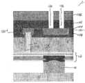
도 1에 따르면, 기판(10)과 집적회로(미도시)를 포함하는 칩(2)이 제공된다. 칩(2)은 웨이퍼의 일 부분이 될 수 있다. 3족, 4족, 또는 5족 요소와 같은 다른 반도체 물질을 포함하고 있더라도, 기판(10)은 벌크 실리콘 기판과 같은 반도체일 수 있다. 트랜지스터(블럭 15에 의해 표기되는)와 같은 능동 소자는 기판(10)의 앞면(10f)에 형성된다. 명세서에서, "후면"이라는 단어는 기판(10)의 면 중 능동 반도체 장치를 가지는 면의 반대쪽 면을 언급한다. 금속 라인과 비아(미도시)를 포함하는 상호접속 구조(12)는 기판(10)의 앞 면(10f)에 형성되고 능동 반도체 소자에 연결된다. 금속 라인 및 비아는 구리 또는 구리합금으로 형성되고, 이미 잘 알려진 다마신(damascene) 공정을 이용하여 형성될 수 있다. 상호접속 구조(12)는 일반적으로 알려진 층간 절연막(inter-layer dielectric, ILD) 및 금속간 절연만(inter-metal dielectric(IMDs))를 포함한다. 본드 패드(14)는 기판(10)의 앞면(10f)에 형성된다.According to FIG. 1, a
TSV(20)는 기판에 형성되고, 앞면(10f)에서부터 기판(10)으로 확장한다. 도 1에 도시된 바와 같이, 일 실시예에서 TSV(20)는 비아 우선 접근법(via-first approach)을 이용하여 형성되어, 상호접속 구조(12) 형성 전에 형성된다. 따라서, TSV(20)는 오직 능동소자를 커버할 수 있는 ILD까지 확장되고, 상호접속 구조(12)내의 IMD 구조내로 확장되지 않는다. 다른 실시예에서, TSV(20)는 비아 마지막 접근법(via-last approach)을 이용하여 형성되고, 상호접속 구조(12) 형성 후에 형성된다. 따라서, TSV(20)는 기판(10)과 상호접속 구조(12)를 모두로 침투한다. 격리층(22)은 TVS(20)의 끝 및 측벽 상에 형성되고, TSV(20)를 기판(10)으로부터 전기적으로 절연한다. 격리층(22)은 일반적으로 실리콘 질화막, 실리콘 산화막(DpFMF 들어, TEOS(tetra-ethyl-ortho-silicate) 산화물과 같은 절연 물질을 이용하여 만든다. 칩(2) 및 이에 대응되는 웨이퍼는 캐리어(25)에 부착된다.The TSV 20 is formed on the substrate and extends from the front surface 10f to the
도 2에 따르면, 후면 그라인딩(grinding)이 수행되어 TSV(20)가 기판(10)의 후면(10b)을 통해 노출된다. 후면 그라인딩은 정지층(stop layer)으로써 TSV(20)를 이용하여 수행될 수 있다. 다음으로, 도 3에 도시된 바와 같이, TSV(20)는 그것의 상부 표면이 기판(10)의 후면(10b)보다 더 낮아지도록 리세스된다. 리세스 깊이(D1)는 약 0.5μm보다 크고, 바람직한 실시예에서는 3μm일 수 있다. 리세싱 결과, 개구(opening)(24)가 형성된다.According to FIG. 2, backside grinding is performed to expose the TSV 20 through the
도 4는 마스크로써 포토레지스트(photoresist)(26)를 이용하여 수행되는 기판(10)의 리세싱을 도시한다. 리세싱 결과, 개구(24)의 수평적 넓이가 TSV(20)의 개구보다 커지도록 증가된다. 비록 도 3에서는, 후면(10b)의 개구(24) 하부(28)가 TSV(20)의 노출단(exposed end)와 같은 레벨이나 다르게는, 하부(28)는 점선으로 표시된 바와 같이, TSV(20)의 노출단보다는 높거나 낮을 수 있다. 개구(24)가 생성되는 그 시간에, (트렌치) 통로(27) 역시 형성된다.4 shows recessing of
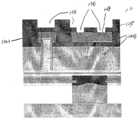
도 5에 대해 언급하면, 유전 격리층(30)이 적층된다. 적층 방법은 비록 일반적으로 사용되는 다른 방법을 이용할 수 있지만, 저온도 화학적 기상 증착법(low-temperature chemical vapor deposition, LTCVD)을 포함한다. 바람직한 실시예에서는, 유전 격리층(30)은 실리콘 질화물(SiNx)를 포함하고, 수백 옴스트롱의 두께를 가질 수 있다. 다음으로, 도 6에 도시된 바와 같이, TSV(20)의 일 단(end)을 오버라잉한 유전 격리층(30)의 일 부분은 포토레지스트(31)를 사용하며, 포토리소그래피 공정을 수행함으로써 비아 개구(33)에서 노출되어, 그 후에 형성되는 범프가 TSV(20)에 전기적으로 연결될 수 있다.Referring to FIG. 5,
도 7 내지 도 9는 재분배 라인(redistribution lines) 및 패드의 형성을 도시한다. 도 7에 대해 설명하면, 티타늄, 티타늄 질화물, 탄탈, 탄탈 질화물 또는 이와 유사한 물질로 구성될 수 있는 도전성 방지층(32)이 예를 들어, 스퍼터링 공정에 의해 형성된다. 도 8에 도시된 것과 같이, 그리고 나서 구리(34)가 도금된다. 구리(34)의 두께는 깊이(D1)(도 3에 도시된)에 의존한다. CMP(chemical mechanical polish)가 금속 구조(36)(36-1, 36-2를 의미함)를 형성하기 위해 수행되고, 그 결과로 형성된 구조가 도 9에 도시된 바와 같다. 금속 구조(36)는 다른 TSVs(미도시)와 실제로 연결될 수 있는 금속 라인(36-1)을 포함할 수 있다. 따라서, 금속 라인(36-1)은 재분배 라인으로써 이용된다. 금속 구조(36-2)는 금속 패드 또는 금속 라인이다. 금속 패드는 (위에서 바라본) TSV(20)의 넓이보다 더 넓은 넓이를 가지고 있고, 메탈 패드는 모든 수평방향으로 TSV(20)의 가장자리를 넘어서 확장될 수 있다. 따라서, 금속 패드(36-2) 및 TSV(20)는 넓은 인터페이스 영역을 가지는 신뢰할 만한 연결을 가지고 따라서 작은 접촉 저항을 가지게 된다. 게다가, TSV(20)에 금속 패드(36-2)를 배열하기 위한 정확성 요구가 완화된다.7-9 illustrate the formation of redistribution lines and pads. Referring to FIG. 7, an
도 10-12A는 범프(42)의 형성을 도시한다. 도 10에 대해 언급하면 유전층(38)은 블랭킷(blanket) 적층된다. 바람직한 실시예에서는, 유전층(38)은 실리콘 질화물(SiNx)로 구성되고, 예를 들어, 약 0.2μm의 두께를 가진다. 다음으로, 도 11에 도시된 바와 같이, 포토레지스트(40)에 의해 개구가 유전층(38)에 형성되어, 금속패드(36-2)가 노출된다. 도 12A는 약 30μm보다 작은 수평적인 수치(길이 또는 두께)를 가지고 있기 때문에 마이크로 범프로써 불릴 수 있는 범프(42)의 형성을 도시한다. 범프(42)의 형성 방법은 전기 화학 도금(electrical chemical plating, ECP), 무전해 도금(electroless plating) 및 이멀젼(immersion) 공정을 포함한다. 형성된 범프(42)는 무전해 니켈 이멀젼 금(electroless nickel immersion gold, ENIG) 구조, 니켈 무전해 팔라듐 이멀젼 금(nickel electroless palladium immersion gold, ENEPIG) 구조, 또는 닉 팔라듐(nick palladium) 구조를 가진다. 비록 도 12A가 범프(42)가 직접적으로 금속 패드(36-2) 상에 있다는 것을 도시하고 있지만, 범프(42)는 또한 금속 패드(36-2) 상에 직접 있지 않고, 실제로는 금속 라인(36-1)과 같은 재분배 라인을 통해 금속 패드(36-2)에 연결될 수 있으며, 이러한 재분배 라인은 메탈 구조(36)의 형성과 동시에 형성될 수 있다.10-12A illustrate the formation of
도 12B는 대체적인 실시예를 도시한다. 금속 패드(36-2) 상에 직접 형성된 범프(42) 대신에, 추가적인 재분배 라인의 층이 형성된다. 예를 들어, 식각 정지층(46), 유전층(48), 비아(50) 및 금속 라인(52)을 포함하는 추가적인 층(60)은 금속 패드(36-2)와 범프(42) 사이에 삽입될 수 있다. 필요하다면 층(60)과 비슷한 더욱 많은 층이 후면 상호접속 구조의 연결성을 향상시키기 위해 층(60) 상에 적층될 수 있다. 층(60)의 형성에 대한 구체적인 설명은 도 18-21에 도시된 것과 본질적으로 같기 때문에, 이하 후술하도록 한다.12B shows an alternative embodiment. Instead of
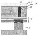
도 13 내지 도 23B는 다른 실시예에 대해 도시한다. 본 실시예에서의 처음 단계는 도 1 및 도 2에서 설명한 것과 같다. 다음으로, 도 13에 대해 언급하면, 기판(10)은 TSV(20)가 기판(10)의 후면으로부터 튀어나올 수 있도록 후면으로부터 에치백(etch back)된다. 대표적인 실시예에서, 에치백 깊이(D2)는 약 0.5μm보다 크고, 약 1μm일 수 있다. 격리층(22)은 또한 TSV(20)의 상부 표면으로부터 뒤에 식각될 수 있고, 예를 들어, TSV(20)의 상부 표면보다 약 0.5μm 낮게 식각될 수 있다. 따라서, TSV(20)의 측벽의 특정부분이 노출된다.13-23B illustrate another embodiment. The first step in this embodiment is the same as described in FIGS. 1 and 2. Next, referring to FIG. 13, the
도 14에 대해 언급하면, 유전층(124)은 기판(10)의 후면에 형성되고, TSV(20)를 덮는다. 일 실시예에서, 유전층(124)은 폴리이머드(polyimide)로 형성되고, 약 2μm보다 큰 두께,바람직하게는 두께가 약 3μm인 두께를 가질 수 있다. 다른 실시예에서는, 다른 유전 물질이 사용될 수 있다.Referring to FIG. 14,
도 15 내지 도 17은 금속 라인의 형성을 묘사한다. 도 15에 따르면, 개구(126)는 예를들어, 포토레지스트(미도시)를 이용한, 유전층(124)의 식각에 의해 형성된다. 일 실시예에서, 개구 형성 공정은 유전층(124)의 바닥 부분(124'층을 의미함)이 기판(10)으로부터 개구(126)를 분리하기 위해 남겨지는 반면, TSV(20)가 개구(126) 중 하나를 통해 노출되기 위해, 예를 들어, 타임 모드를 이용하여 제어된다.15-17 depict the formation of metal lines. According to FIG. 15, the
도 16에 대해 언급하면, 프리-클린(pre-clean)이 수행되고, 도전성 배리어층(128)이 스퍼터링(sputtering)과 같은 공정에 의해 적층된다. 도전성 방지층(128)은 티타늄, 탄탈, 또는 이와 같은 물질을 포함한다. 금속성 물질(130)이 유전층(124)의 상부 표면보다 높은 레벨로 도금된다. 금속 물질(130)은 알루미늄, 텅스텐과 같은 다른 물질을 사용할 수 있더라도 구리를 포함한다. 도 17에 도시된 바와 같이, CMP가 수행되고, 그리고 금속 라인/패드(132)(132-1,132-2를 의미함)가 형성된다. 금속 라인(132-2)은 칩에서 TSVs 중 하나에 전기적으로 연결된다. 따라서, 금속 라인(132-2)은 재분배 라인으로서 이용된다. 금속 구조(132-1)는 금속 패드 또는 금속 트레이스(trace)일 수 있다. 금속 패드는 TSV(20)의 면적보다 큰 면적(상부에서부터 본)를 가질 수 있어서, 상부에서 바라보면, 금속 패드(132-1)는 모든 측면 방향으로 TSV(20)의 가장자리에서 모든 측면 방향으로 확장될 수 있다.Referring to FIG. 16, pre-clean is performed, and the
도 18 내지 도 21은 상호접속의 추가적인 층을 형성하는 것을 보여준다. 도 18에 대해 언급하면, 유전층(125)은 형성된다. 일 실시예에서, 유전층(125)은 약 2.5μm과 같은 몇몇의 미크론(micron)의 두께를 가질 수 있는 폴리이머드로 형성될 수 있다. 포토레지스트(134)가 인가되고 나서 패턴된다. 비아 개구(136)는 패턴된 포토레지스트(134)를 통해 금속 라인(132-2)이 노출될 때까지 유전층(125)을 식각함으로써 형성된다.18-21 show forming additional layers of interconnect. Referring to FIG. 18,
도 19에 대해 언급하면, 포토레지스트(134)가 제거되고, 추가적인 포토레지스트(140)가 형성되고 패턴된다. 트렌치 개구(138)는 도 20에 도시된 바와 같이, 패턴된 포토레지스트(140)를 통해 유전층(125)이 더 식각됨으로써 형성된다. 식각은 타임 모드를 이용하여 수행되어 식각이 유전층(125)의 중간 레벨에서 정지될 수 있다. 포토레지스트(140)는 애싱(ashing) 공정과 같은 공정에 의해 제거될 수 있다. 도 18 내지 도 20에서 보여준 단계가 비아 개구(136)가 트렌치 개구(138)가 형성되기 전에 형성되는 비아 우선 접근법임을 알 수 있다. 해당 기술 분야의 당업자는 도 20에 도시된 구조가 도 19 및 도 20에 도시된 단계가 도 18에 도시된 단계 이전에 수행되는 트렌치 우선 접근법을 이용하여 형성될 수 있다는 것을 알 수 있다.Referring to FIG. 19,
도 21은 도전성 배리어층(148)(예를 들어, Ti 층)을 적층하는 단계, 구리를 도금하는 단계, 및 여분의 구리를 제거하기 위해 CMP를 수행하는 과정을 포함하는, 금속 라인(144)과 비아(146)를 포함하는 다마신 구조의 형성을 도시한다.21 illustrates a
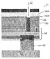
도 22 내지 도 23A는 유전층(40) 및 범프(42)의 형성을 도시한다. 형성 공정은 앞선 실시예에서 설명한 것과 본질적으로 같을 수 있으므로, 여기서 다시 반복하지 않는다. 도 23B는 금속 라인(144)과 비아(146)가 유전층(124) 안에 형성되는 대체적인 실시예를 도시한다.22-23A illustrate the formation of
도 24 내지 도 29B는 또 다른 실시예를 도시한다. 본 실시예의 처음 단계는 도 1 및 도 2에 도시된 것과 같다. 다음으로, 도 24에 도시된 바와 같이, 식각 정지층(220)이 형성된다. 일 실시예에서, 식각 정지층(220)은 실리콘 질화물에 의해 형성되고, 예를 들어, 약 750Å의 두께를 가질 수 있다. 유전층(222)은 식각 정지층(220) 상에 형성된다. 일 실시예에서, 유전층(222)은 다양한 화학 기상 적층법(CVD) 중 하나를 이용하여 형성될 수 있고, 예를 들어, 산화물로 구성될 수 있다. CVD 유전층(222)의 두께는 예를 들어, 약 8KÅ일 수 있다. 다른 실시예에서, 유전층(222)은 폴리이머드로 형성될 수 있고, CVD를 이용하여 형성한 것보다 상당히 큰 두께를 가질 수 있다. 폴리이머드에 의해 형성된 유전층(222)의 두께는 약 2μm보다 크고, 바람직한 실시예에서는 약 5μm일 수 있다.24-29B show yet another embodiment. The first step of this embodiment is as shown in Figs. Next, as shown in FIG. 24, an
도 25 내지 도 27은 비아 개구(226) 및 트렌치 개구(228)의 형성을 도시한다. 자세한 형성과정은 도 18 내지 도 20에서 설명한 것과 본질적으로 같으므로, 여기서는 반복하여 설명하지 않는다. 다음으로, 도 28에 도시된 바와 같이, 비아(232) 및 구리에 의해 형성될 수 있는 오버라잉 금속 라인(234)을 포함하는 듀얼 다마신 구조가 형성된다. 도전성 방지층(236) 또한 형성된다.25-27 illustrate the formation of via
도 29A는 유전층(40)과 범프(42)의 형성을 도시한다. 유전체(40) 및 범프(42)의 물질 및 형성과정은 본질적으로 도 10 내지 도 12A에서 설명한 바와 같다. 도 29B는 추가적인 듀얼 다마신 구조를 포함하는 추가적인 상호접속 층(60)을 가지는 대체적인 실시예를 도시한다. 필요하다면, 더욱 많은 상호접속 층이 삽입될 수 있다.29A illustrates the formation of
상술한 실시예는 몇몇의 유리한 특징이 있다. 듀얼 다마신 공정을 이용하여 후면의 상호접속 구조를 형성함으로써, 복수의 상호접속 층이 훌륭한 라우팅(routing) 능력을 제공할 수 있도록 적층될 수 있다.The embodiment described above has several advantageous features. By forming a backside interconnect structure using a dual damascene process, multiple interconnect layers can be stacked to provide good routing capabilities.
TSVs의 접촉을 위한 금속 패드(도 10의 36-2 및 도 17의 132-1)를 형성하기 위해 기판을 리세스함으로써, 금속 패드는 TSVs가 금속 패드의 정렬에서 정확한 요구에 관대하기 위해, 큰 사이즈를 가질 수 있다. 게다가, 금속 패드 및 밑에 있는 TSVs는 큰 접촉 면적을 가지므로, 접촉 저항이 감소된다.By recessing the substrate to form metal pads (36-2 in FIG. 10 and 132-1 in FIG. 17) for the contact of the TSVs, the metal pads are large in order for the TSVs to tolerate the exact demands of the metal pads in alignment. It may have a size. In addition, the metal pads and underlying TSVs have a large contact area, so that the contact resistance is reduced.
이상에서는 본 발명의 바람직한 실시예에 대하여 도시하고 설명하였지만, 본 발명은 상술한 특정의 실시예에 한정되지 아니하며, 청구범위에서 청구하는 본 발명의 요지를 벗어남이 없이 당해 발명이 속하는 기술분야에서 통상의 지식을 가진자에 의해 다양한 변형실시가 가능한 것은 물론이고, 이러한 변형실시들은 본 발명의 기술적 사상이나 전망으로부터 개별적으로 이해되어져서는 안될 것이다.While the present invention has been particularly shown and described with reference to exemplary embodiments thereof, it is clearly understood that the same is by way of illustration and example only and is not to be construed as limiting the scope of the invention as defined by the appended claims. It will be understood by those skilled in the art that various changes in form and details may be made therein without departing from the spirit and scope of the invention.
Claims (10)
Translated fromKorean능동 반도체 소자들을 갖는 앞면과 상기 앞면의 반대편에 있는 후면을 구비하는 반도체 기판;
상기 반도체 기판을 관통하는 제1 도전성 비아;
상기 반도체 기판의 후면에 있는 금속 구조로서, 상기 반도체 기판의 리세스된(recessed) 영역에 형성되고 접촉 저항을 감소시키기 위해 상기 제1 도전성 비아 위를 덮고 상기 제1 도전성 비아와 접촉하는 금속 패드, 및 상기 금속 패드 상의 듀얼 다마신(dual damascene) 구조 - 상기 듀얼 다마신 구조는 제2 도전성 비아 및 상기 제2 도전성 비아 위를 덮고 상기 제2 도전성 비아와 접촉하는 금속 라인을 포함함 - 를 포함하는 상기 금속 구조; 및
상기 금속 라인 위를 덮는 범프(bump)
를 포함하는 집적회로 구조.In the integrated circuit structure,
A semiconductor substrate having a front side having active semiconductor elements and a back side opposite the front side;
A first conductive via penetrating the semiconductor substrate;
A metal structure on a back surface of the semiconductor substrate, the metal pad being formed in a recessed region of the semiconductor substrate and overlying the first conductive via and in contact with the first conductive via to reduce contact resistance, And a dual damascene structure on the metal pad, the dual damascene structure comprising a second conductive via and a metal line overlying the second conductive via and in contact with the second conductive via. The metal structure; And
A bump over the metal line
Integrated circuit structure comprising a.
상기 금속 패드는,
상기 제1 도전성 비아의 상부 표면과 접촉하는 제1 바닥면; 및
상기 반도체 기판의 후면보다는 높고, 상기 제1 바닥면보다는 낮은 제2 바닥면을 더 포함하는 것인 집적회로 구조.The method of claim 1,
The metal pad,
A first bottom surface in contact with the top surface of the first conductive via; And
And a second bottom surface higher than a rear surface of the semiconductor substrate and lower than the first bottom surface.
상기 듀얼 다마신 구조는 상기 금속 패드 상의 유전층 내에 있는 것인 집적회로 구조.The method of claim 1,
The dual damascene structure is in a dielectric layer on the metal pad.
상기 금속 패드의 모든 수평적 치수(dimension)들은 상기 제1 도전성 비아의 각각의 수평적 치수들보다 큰 것인 집적회로 구조.The method of claim 1,
Wherein all horizontal dimensions of the metal pad are greater than respective horizontal dimensions of the first conductive via.
Applications Claiming Priority (4)
| Application Number | Priority Date | Filing Date | Title |
|---|---|---|---|
| US24477309P | 2009-09-22 | 2009-09-22 | |
| US61/244,773 | 2009-09-22 | ||
| US12/832,019US8791549B2 (en) | 2009-09-22 | 2010-07-07 | Wafer backside interconnect structure connected to TSVs |
| US12/832,019 | 2010-07-07 |
Publications (2)
| Publication Number | Publication Date |
|---|---|
| KR20110033022A KR20110033022A (en) | 2011-03-30 |
| KR101319701B1true KR101319701B1 (en) | 2013-10-17 |
Family
ID=43755919
Family Applications (1)
| Application Number | Title | Priority Date | Filing Date |
|---|---|---|---|
| KR1020100080460AActiveKR101319701B1 (en) | 2009-09-22 | 2010-08-19 | Wafer Backside Interconnect Structure Connected To TSVs |
Country Status (5)
| Country | Link |
|---|---|
| US (4) | US8791549B2 (en) |
| JP (1) | JP5271985B2 (en) |
| KR (1) | KR101319701B1 (en) |
| CN (1) | CN102024781B (en) |
| TW (1) | TWI453879B (en) |
Families Citing this family (72)
| Publication number | Priority date | Publication date | Assignee | Title |
|---|---|---|---|---|
| US8513119B2 (en) | 2008-12-10 | 2013-08-20 | Taiwan Semiconductor Manufacturing Company, Ltd. | Method of forming bump structure having tapered sidewalls for stacked dies |
| US20100171197A1 (en)* | 2009-01-05 | 2010-07-08 | Hung-Pin Chang | Isolation Structure for Stacked Dies |
| US8791549B2 (en) | 2009-09-22 | 2014-07-29 | Taiwan Semiconductor Manufacturing Company, Ltd. | Wafer backside interconnect structure connected to TSVs |
| US8466059B2 (en) | 2010-03-30 | 2013-06-18 | Taiwan Semiconductor Manufacturing Company, Ltd. | Multi-layer interconnect structure for stacked dies |
| US8716867B2 (en) | 2010-05-12 | 2014-05-06 | Taiwan Semiconductor Manufacturing Company, Ltd. | Forming interconnect structures using pre-ink-printed sheets |
| US9190325B2 (en)* | 2010-09-30 | 2015-11-17 | Taiwan Semiconductor Manufacturing Company, Ltd. | TSV formation |
| KR101697573B1 (en)* | 2010-11-29 | 2017-01-19 | 삼성전자 주식회사 | Semiconductor device, fabricating method thereof, and semiconductor package comprising the semiconductor device |
| KR101789765B1 (en)* | 2010-12-16 | 2017-11-21 | 삼성전자주식회사 | Semiconductor device and method of forming the same |
| KR20120090417A (en)* | 2011-02-08 | 2012-08-17 | 삼성전자주식회사 | Semiconductor device and method of manufacturing a semiconductor device |
| US8853072B2 (en)* | 2011-06-06 | 2014-10-07 | Micron Technology, Inc. | Methods of forming through-substrate interconnects |
| JP2012256679A (en)* | 2011-06-08 | 2012-12-27 | Elpida Memory Inc | Semiconductor device and manufacturing method of the same |
| US8900994B2 (en) | 2011-06-09 | 2014-12-02 | Taiwan Semiconductor Manufacturing Company, Ltd. | Method for producing a protective structure |
| CN103000571B (en)* | 2011-09-19 | 2015-07-08 | 中芯国际集成电路制造(上海)有限公司 | Semiconductor device and manufacturing method thereof |
| US9142510B2 (en) | 2011-10-28 | 2015-09-22 | Intel Corporation | 3D interconnect structure comprising through-silicon vias combined with fine pitch backside metal redistribution lines fabricated using a dual damascene type approach |
| KR101620767B1 (en)* | 2011-10-28 | 2016-05-12 | 인텔 코포레이션 | 3d interconnect structure comprising fine pitch single damascene backside metal redistribution lines combined with through-silicon vias |
| US20130313710A1 (en)* | 2012-05-22 | 2013-11-28 | Micron Technology, Inc. | Semiconductor Constructions and Methods of Forming Semiconductor Constructions |
| KR101931115B1 (en) | 2012-07-05 | 2018-12-20 | 삼성전자주식회사 | Semiconductor device and method of forming the same |
| KR20140023055A (en)* | 2012-08-16 | 2014-02-26 | 에스케이하이닉스 주식회사 | Semiconductor device and method for forming using the same |
| KR102021884B1 (en)* | 2012-09-25 | 2019-09-18 | 삼성전자주식회사 | Semiconductor Device Having Backside Bonding Structure |
| US8859425B2 (en) | 2012-10-15 | 2014-10-14 | Micron Technology, Inc. | Devices, systems, and methods related to forming through-substrate vias with sacrificial plugs |
| KR102018885B1 (en)* | 2012-12-20 | 2019-09-05 | 삼성전자주식회사 | Semiconductor devices having through vias and methods for fabricating the same |
| US10483132B2 (en)* | 2012-12-28 | 2019-11-19 | Taiwan Semiconductor Manufacturing Company, Ltd. | Post-passivation interconnect structure and method of forming the same |
| US9466578B2 (en)* | 2013-12-20 | 2016-10-11 | Qualcomm Incorporated | Substrate comprising improved via pad placement in bump area |
| US20150179580A1 (en)* | 2013-12-24 | 2015-06-25 | United Microelectronics Corp. | Hybrid interconnect structure and method for fabricating the same |
| US9093503B1 (en)* | 2014-01-03 | 2015-07-28 | International Business Machines Corporation | Semiconductor chip with a dual damascene wire and through-substrate via (TSV) structure |
| US9865523B2 (en)* | 2014-01-17 | 2018-01-09 | Taiwan Semiconductor Manufacturing Company, Ltd. | Robust through-silicon-via structure |
| KR102222485B1 (en)* | 2014-09-18 | 2021-03-04 | 에스케이하이닉스 주식회사 | Semiconductor device having through via, semiconductor package including the same and the method for manufacturing semiconductor device |
| DE102014115105B4 (en) | 2014-10-09 | 2023-06-22 | Taiwan Semiconductor Manufacturing Company, Ltd. | Semiconductor device and method of manufacturing a semiconductor device |
| TWI582918B (en)* | 2014-11-12 | 2017-05-11 | 精材科技股份有限公司 | Chip package and manufacturing method thereof |
| KR102279729B1 (en)* | 2014-12-01 | 2021-07-21 | 삼성전자주식회사 | Semiconductor Devices Having a TSV, a Frontside Bumping Pad, and a Backside Bumping Pad |
| US9431343B1 (en) | 2015-03-11 | 2016-08-30 | Samsung Electronics Co., Ltd. | Stacked damascene structures for microelectronic devices |
| US9666523B2 (en) | 2015-07-24 | 2017-05-30 | Nxp Usa, Inc. | Semiconductor wafers with through substrate vias and back metal, and methods of fabrication thereof |
| US9472490B1 (en) | 2015-08-12 | 2016-10-18 | GlobalFoundries, Inc. | IC structure with recessed solder bump area and methods of forming same |
| KR20170023643A (en) | 2015-08-24 | 2017-03-06 | 삼성전자주식회사 | Semiconductor device and method of manufacturing the same |
| US10121812B2 (en)* | 2015-12-29 | 2018-11-06 | Taiwan Semiconductor Manufacturing Co., Ltd. | Stacked substrate structure with inter-tier interconnection |
| US10276402B2 (en)* | 2016-03-21 | 2019-04-30 | Taiwan Semiconductor Manufacturing Co., Ltd. | Semiconductor package and manufacturing process thereof |
| JP6955864B2 (en)* | 2016-12-26 | 2021-10-27 | ラピスセミコンダクタ株式会社 | Semiconductor devices and methods for manufacturing semiconductor devices |
| KR102489216B1 (en)* | 2017-01-20 | 2023-01-16 | 도쿄엘렉트론가부시키가이샤 | Interconnection structure and method of forming the same |
| KR102406573B1 (en)* | 2017-04-28 | 2022-06-09 | 삼성전자주식회사 | Semiconductor device and method for manufacturing the same |
| CN112164688B (en)* | 2017-07-21 | 2023-06-13 | 联华电子股份有限公司 | Chip stacking structure and manufacturing method of chip stacking structure |
| US10515921B2 (en)* | 2017-07-27 | 2019-12-24 | Taiwan Semiconductor Manufacturing Co., Ltd. | Semiconductor package and method of fabricating semiconductor package |
| US10636758B2 (en)* | 2017-10-05 | 2020-04-28 | Texas Instruments Incorporated | Expanded head pillar for bump bonds |
| US11843020B2 (en) | 2017-10-30 | 2023-12-12 | Samsung Electronics Co., Ltd. | Image sensor |
| KR102542614B1 (en) | 2017-10-30 | 2023-06-15 | 삼성전자주식회사 | Image sensor |
| US11521923B2 (en)* | 2018-05-24 | 2022-12-06 | Intel Corporation | Integrated circuit package supports |
| KR102665246B1 (en)* | 2018-07-03 | 2024-05-09 | 삼성전자주식회사 | Semiconductor device and method for fabricating thereof |
| MY203745A (en)* | 2018-07-31 | 2024-07-17 | Intel Corp | Micro through-silicon via for transistor density scaling |
| KR102635832B1 (en) | 2018-09-28 | 2024-02-15 | 삼성전자주식회사 | Semiconductor device and method of fabricating the same |
| US10727124B2 (en) | 2018-10-29 | 2020-07-28 | International Business Machines Corporation | Structure and method for forming fully-aligned trench with an up-via integration scheme |
| JP7353748B2 (en)* | 2018-11-29 | 2023-10-02 | キヤノン株式会社 | Semiconductor device manufacturing method and semiconductor device |
| US10770427B1 (en)* | 2019-06-27 | 2020-09-08 | Taiwan Semiconductor Manufacturing Co., Ltd. | Chip package structure and method for forming the same |
| US11195810B2 (en) | 2019-08-23 | 2021-12-07 | Taiwan Semiconductor Manufacturing Company, Ltd. | Bonding structure and method of forming same |
| US11398408B2 (en)* | 2019-09-24 | 2022-07-26 | Advanced Semiconductor Engineering, Inc. | Semiconductor substrate with trace connected to via at a level within a dielectric layer |
| US11094580B2 (en)* | 2019-10-01 | 2021-08-17 | International Business Machines Corporation | Structure and method to fabricate fully aligned via with reduced contact resistance |
| US11217481B2 (en)* | 2019-11-08 | 2022-01-04 | International Business Machines Corporation | Fully aligned top vias |
| US11295978B2 (en) | 2020-04-29 | 2022-04-05 | International Business Machines Corporation | Interconnects having spacers for improved top via critical dimension and overlay tolerance |
| KR20210133524A (en) | 2020-04-29 | 2021-11-08 | 삼성전자주식회사 | Interconnection structure and Semiconductor package including the same |
| US11404378B2 (en)* | 2020-11-24 | 2022-08-02 | Omnivision Technologies, Inc. | Semiconductor device with buried metal pad, and methods for manufacture |
| US12205997B2 (en)* | 2021-03-12 | 2025-01-21 | Taiwan Semiconductor Manufacturing Co., Ltd. | Integrated circuit including backside conductive vias |
| KR20220129924A (en)* | 2021-03-17 | 2022-09-26 | 삼성전자주식회사 | Interposer, method for fabricating the same, and semiconductor package having the same |
| US12300492B2 (en) | 2021-03-26 | 2025-05-13 | Changxin Memory Technologies, Inc. | Method for manufacturing semiconductor structure, and semiconductor structure |
| US12100670B2 (en) | 2021-03-26 | 2024-09-24 | Changxin Memory Technologies, Inc. | Method for manufacturing semiconductor structure and semiconductor structure |
| CN113078119B (en)* | 2021-03-26 | 2022-03-18 | 长鑫存储技术有限公司 | Manufacturing method of semiconductor structure and semiconductor structure |
| KR20220167423A (en) | 2021-06-11 | 2022-12-21 | 삼성전자주식회사 | Semiconductor device including through electrodes |
| US12176311B2 (en)* | 2021-07-05 | 2024-12-24 | Changxin Memory Technologies, Inc. | Micro bump, method for forming micro bump, chip interconnection structure and chip interconnection method |
| KR20230034506A (en)* | 2021-09-03 | 2023-03-10 | 삼성전자주식회사 | Method of fabricating a semiconductor device using gas blowing agent |
| US12087691B2 (en) | 2021-09-21 | 2024-09-10 | International Business Machines Corporation | Semiconductor structures with backside gate contacts |
| KR102681185B1 (en)* | 2021-09-24 | 2024-07-04 | 한국기계연구원 | Micro-led display panel and method for manufacturing the same |
| US12002758B2 (en) | 2021-11-04 | 2024-06-04 | International Business Machines Corporation | Backside metal-insulator-metal (MIM) capacitors extending through backside interlayer dielectric (BILD) layer or semiconductor layer and partly through dielectric layer |
| US20230378016A1 (en)* | 2022-05-23 | 2023-11-23 | Taiwan Semiconductor Manufacturing Company, Ltd. | Techniques for heat dispersion in 3d integrated circuit |
| KR20240019456A (en)* | 2022-08-04 | 2024-02-14 | 삼성전자주식회사 | Semiconductor device |
| CN119008562B (en)* | 2024-10-23 | 2024-12-27 | 湖北星辰技术有限公司 | Semiconductor device, manufacturing method thereof and memory system |
Citations (4)
| Publication number | Priority date | Publication date | Assignee | Title |
|---|---|---|---|---|
| KR20060054688A (en)* | 2004-11-16 | 2006-05-23 | 강준모 | Semiconductor device having rear input / output terminal and manufacturing method thereof |
| KR20060054690A (en)* | 2004-11-16 | 2006-05-23 | 강준모 | Semiconductor device having rear input / output terminal and manufacturing method thereof |
| KR20060054689A (en)* | 2004-11-16 | 2006-05-23 | 강준모 | Semiconductor device having rear input / output terminal and manufacturing method thereof |
| KR20080101635A (en)* | 2007-05-18 | 2008-11-21 | 삼성전자주식회사 | Semiconductor package, manufacturing method thereof, and package module and electronic product using semiconductor package |
Family Cites Families (129)
| Publication number | Priority date | Publication date | Assignee | Title |
|---|---|---|---|---|
| GB2034900B (en)* | 1978-11-17 | 1982-10-20 | Marconi Instruments Ltd | Spectrum analyser |
| US4872750A (en)* | 1982-07-14 | 1989-10-10 | Nec Home Electronics Ltd. | Image projection apparatus |
| US4799050A (en)* | 1986-10-23 | 1989-01-17 | Litton Systems Canada Limited | Full color liquid crystal display |
| JP2554724B2 (en)* | 1987-12-11 | 1996-11-13 | 株式会社リコー | Optical scanning optical system using laser diode array |
| JPH05211239A (en)* | 1991-09-12 | 1993-08-20 | Texas Instr Inc <Ti> | Interconnection structure of integrated circuit and method for formation of it |
| US5426072A (en)* | 1993-01-21 | 1995-06-20 | Hughes Aircraft Company | Process of manufacturing a three dimensional integrated circuit from stacked SOI wafers using a temporary silicon substrate |
| DE4314907C1 (en)* | 1993-05-05 | 1994-08-25 | Siemens Ag | Method for producing semiconductor components making electrically conducting contact with one another vertically |
| US5391917A (en)* | 1993-05-10 | 1995-02-21 | International Business Machines Corporation | Multiprocessor module packaging |
| US5646067A (en)* | 1995-06-05 | 1997-07-08 | Harris Corporation | Method of bonding wafers having vias including conductive material |
| US6469683B1 (en)* | 1996-01-17 | 2002-10-22 | Nippon Telegraph And Telephone Corporation | Liquid crystal optical device |
| EP0948808A4 (en) | 1996-10-29 | 2000-05-10 | Trusi Technologies Llc | INTEGRATED CIRCUITS AND MANUFACTURING METHODS THEREOF |
| US6882030B2 (en) | 1996-10-29 | 2005-04-19 | Tru-Si Technologies, Inc. | Integrated circuit structures with a conductor formed in a through hole in a semiconductor substrate and protruding from a surface of the substrate |
| JPH10163315A (en)* | 1996-11-28 | 1998-06-19 | Nec Ic Microcomput Syst Ltd | Semiconductor circuit device |
| US6037822A (en)* | 1997-09-30 | 2000-03-14 | Intel Corporation | Method and apparatus for distributing a clock on the silicon backside of an integrated circuit |
| US5998292A (en) | 1997-11-12 | 1999-12-07 | International Business Machines Corporation | Method for making three dimensional circuit integration |
| JP3600470B2 (en)* | 1998-06-22 | 2004-12-15 | パイオニア株式会社 | Plasma display panel |
| KR100281897B1 (en)* | 1998-07-21 | 2001-03-02 | 윤종용 | Semiconductor device having conduction layer and fabrication method thereof |
| US6706189B2 (en)* | 1998-10-09 | 2004-03-16 | Zenon Environmental Inc. | Cyclic aeration system for submerged membrane modules |
| KR100730433B1 (en)* | 1998-10-28 | 2007-06-19 | 다이니폰 인사츠 가부시키가이샤 | LCD Display |
| JP3532788B2 (en)* | 1999-04-13 | 2004-05-31 | 唯知 須賀 | Semiconductor device and manufacturing method thereof |
| JP3998373B2 (en)* | 1999-07-01 | 2007-10-24 | 株式会社ルネサステクノロジ | Manufacturing method of semiconductor integrated circuit device |
| US6785028B1 (en)* | 1999-11-24 | 2004-08-31 | Ricoh Company, Ltd. | Optical scanning device having a temperature compensation unit |
| US6322903B1 (en)* | 1999-12-06 | 2001-11-27 | Tru-Si Technologies, Inc. | Package of integrated circuits and vertical integration |
| US6417087B1 (en)* | 1999-12-16 | 2002-07-09 | Agere Systems Guardian Corp. | Process for forming a dual damascene bond pad structure over active circuitry |
| US6292285B1 (en)* | 1999-12-20 | 2001-09-18 | Xerox Corporation | Single rotating polygon mirror with v-shaped facets for a multiple beam ROS |
| JP3626058B2 (en)* | 2000-01-25 | 2005-03-02 | Necエレクトロニクス株式会社 | Manufacturing method of semiconductor device |
| JP2001291720A (en) | 2000-04-05 | 2001-10-19 | Hitachi Ltd | Semiconductor integrated circuit device and method of manufacturing semiconductor integrated circuit device |
| US6444576B1 (en)* | 2000-06-16 | 2002-09-03 | Chartered Semiconductor Manufacturing, Ltd. | Three dimensional IC package module |
| US7053465B2 (en) | 2000-11-28 | 2006-05-30 | Texas Instruments Incorporated | Semiconductor varactor with reduced parasitic resistance |
| US6498381B2 (en) | 2001-02-22 | 2002-12-24 | Tru-Si Technologies, Inc. | Semiconductor structures having multiple conductive layers in an opening, and methods for fabricating same |
| US6717254B2 (en)* | 2001-02-22 | 2004-04-06 | Tru-Si Technologies, Inc. | Devices having substrates with opening passing through the substrates and conductors in the openings, and methods of manufacture |
| US6696360B2 (en)* | 2001-03-15 | 2004-02-24 | Micron Technology, Inc. | Barrier-metal-free copper damascene technology using atomic hydrogen enhanced reflow |
| JP2002296714A (en)* | 2001-03-30 | 2002-10-09 | Fuji Photo Film Co Ltd | Method for reading radiographic image information |
| US7224063B2 (en)* | 2001-06-01 | 2007-05-29 | International Business Machines Corporation | Dual-damascene metallization interconnection |
| KR100404479B1 (en)* | 2001-06-21 | 2003-11-05 | 주식회사 하이닉스반도체 | Method for forming the dual damascene line |
| US6599778B2 (en)* | 2001-12-19 | 2003-07-29 | International Business Machines Corporation | Chip and wafer integration process using vertical connections |
| EP1472730A4 (en)* | 2002-01-16 | 2010-04-14 | Mann Alfred E Found Scient Res | HOUSING FOR ELECTRONIC CIRCUITS WITH REDUCED SIZE |
| US6762076B2 (en)* | 2002-02-20 | 2004-07-13 | Intel Corporation | Process of vertically stacking multiple wafers supporting different active integrated circuit (IC) devices |
| US6642081B1 (en)* | 2002-04-11 | 2003-11-04 | Robert Patti | Interlocking conductor method for bonding wafers to produce stacked integrated circuits |
| CN1215551C (en)* | 2002-04-12 | 2005-08-17 | 台湾积体电路制造股份有限公司 | Dual damascene method for blocking gas release and protrusion structure generation |
| JP2003318178A (en)* | 2002-04-24 | 2003-11-07 | Seiko Epson Corp | Semiconductor device and its manufacturing method, circuit board, and electronic equipment |
| US6800930B2 (en) | 2002-07-31 | 2004-10-05 | Micron Technology, Inc. | Semiconductor dice having back side redistribution layer accessed using through-silicon vias, and assemblies |
| JP3774715B2 (en)* | 2002-10-21 | 2006-05-17 | キヤノン株式会社 | Projection display |
| US7030481B2 (en) | 2002-12-09 | 2006-04-18 | Internation Business Machines Corporation | High density chip carrier with integrated passive devices |
| US7354798B2 (en)* | 2002-12-20 | 2008-04-08 | International Business Machines Corporation | Three-dimensional device fabrication method |
| JP4072677B2 (en) | 2003-01-15 | 2008-04-09 | セイコーエプソン株式会社 | Semiconductor chip, semiconductor wafer, semiconductor device and manufacturing method thereof, circuit board, and electronic equipment |
| JP2004297019A (en) | 2003-03-28 | 2004-10-21 | Seiko Epson Corp | Semiconductor device, circuit board and electronic equipment |
| US6841883B1 (en)* | 2003-03-31 | 2005-01-11 | Micron Technology, Inc. | Multi-dice chip scale semiconductor components and wafer level methods of fabrication |
| US6908856B2 (en)* | 2003-04-03 | 2005-06-21 | Interuniversitair Microelektronica Centrum (Imec) | Method for producing electrical through hole interconnects and devices made thereof |
| JP4248928B2 (en)* | 2003-05-13 | 2009-04-02 | ローム株式会社 | Semiconductor chip manufacturing method, semiconductor device manufacturing method, semiconductor chip, and semiconductor device |
| US6924551B2 (en)* | 2003-05-28 | 2005-08-02 | Intel Corporation | Through silicon via, folded flex microelectronic package |
| US7111149B2 (en)* | 2003-07-07 | 2006-09-19 | Intel Corporation | Method and apparatus for generating a device ID for stacked devices |
| US6897125B2 (en)* | 2003-09-17 | 2005-05-24 | Intel Corporation | Methods of forming backside connections on a wafer stack |
| TWI251313B (en)* | 2003-09-26 | 2006-03-11 | Seiko Epson Corp | Intermediate chip module, semiconductor device, circuit board, and electronic device |
| US7335972B2 (en)* | 2003-11-13 | 2008-02-26 | Sandia Corporation | Heterogeneously integrated microsystem-on-a-chip |
| US6878616B1 (en)* | 2003-11-21 | 2005-04-12 | International Business Machines Corporation | Low-k dielectric material system for IC application |
| US7060601B2 (en)* | 2003-12-17 | 2006-06-13 | Tru-Si Technologies, Inc. | Packaging substrates for integrated circuits and soldering methods |
| US7049170B2 (en)* | 2003-12-17 | 2006-05-23 | Tru-Si Technologies, Inc. | Integrated circuits and packaging substrates with cavities, and attachment methods including insertion of protruding contact pads into cavities |
| JP4467318B2 (en) | 2004-01-28 | 2010-05-26 | Necエレクトロニクス株式会社 | Semiconductor device, chip alignment method for multi-chip semiconductor device, and method for manufacturing chip for multi-chip semiconductor device |
| JP4339152B2 (en)* | 2004-03-08 | 2009-10-07 | 富士通マイクロエレクトロニクス株式会社 | Method for forming wiring structure |
| JP4074862B2 (en) | 2004-03-24 | 2008-04-16 | ローム株式会社 | Semiconductor device manufacturing method, semiconductor device, and semiconductor chip |
| JP4327644B2 (en)* | 2004-03-31 | 2009-09-09 | Necエレクトロニクス株式会社 | Manufacturing method of semiconductor device |
| JP4439976B2 (en)* | 2004-03-31 | 2010-03-24 | Necエレクトロニクス株式会社 | Semiconductor device and manufacturing method thereof |
| CN101048868B (en) | 2004-08-20 | 2010-06-09 | 佐伊科比株式会社 | Method for manufacturing semiconductor device having three-dimensional stacked structure |
| US7300857B2 (en) | 2004-09-02 | 2007-11-27 | Micron Technology, Inc. | Through-wafer interconnects for photoimager and memory wafers |
| US7262495B2 (en)* | 2004-10-07 | 2007-08-28 | Hewlett-Packard Development Company, L.P. | 3D interconnect with protruding contacts |
| JP2006339584A (en)* | 2005-06-06 | 2006-12-14 | Sharp Corp | Semiconductor device and manufacturing method thereof |
| US7297574B2 (en) | 2005-06-17 | 2007-11-20 | Infineon Technologies Ag | Multi-chip device and method for producing a multi-chip device |
| US7795134B2 (en) | 2005-06-28 | 2010-09-14 | Micron Technology, Inc. | Conductive interconnect structures and formation methods using supercritical fluids |
| US7429529B2 (en)* | 2005-08-05 | 2008-09-30 | Farnworth Warren M | Methods of forming through-wafer interconnects and structures resulting therefrom |
| US7863187B2 (en)* | 2005-09-01 | 2011-01-04 | Micron Technology, Inc. | Microfeature workpieces and methods for forming interconnects in microfeature workpieces |
| US7772116B2 (en)* | 2005-09-01 | 2010-08-10 | Micron Technology, Inc. | Methods of forming blind wafer interconnects |
| US7633167B2 (en)* | 2005-09-29 | 2009-12-15 | Nec Electronics Corporation | Semiconductor device and method for manufacturing same |
| US20070081239A1 (en)* | 2005-10-06 | 2007-04-12 | May Gregory J | Optical characteristics of a screen |
| US7609442B2 (en)* | 2005-10-13 | 2009-10-27 | Hewlett-Packard Development Company, L.P. | Synchronizing screen |
| TW200733270A (en)* | 2005-10-19 | 2007-09-01 | Koninkl Philips Electronics Nv | Redistribution layer for wafer-level chip scale package and method therefor |
| JP5073946B2 (en) | 2005-12-27 | 2012-11-14 | 新光電気工業株式会社 | Semiconductor device and manufacturing method of semiconductor device |
| US7902643B2 (en)* | 2006-08-31 | 2011-03-08 | Micron Technology, Inc. | Microfeature workpieces having interconnects and conductive backplanes, and associated systems and methods |
| US7514775B2 (en)* | 2006-10-09 | 2009-04-07 | Taiwan Semiconductor Manufacturing Co., Ltd. | Stacked structures and methods of fabricating stacked structures |
| US7544605B2 (en) | 2006-11-21 | 2009-06-09 | Freescale Semiconductor, Inc. | Method of making a contact on a backside of a die |
| JP4415984B2 (en)* | 2006-12-06 | 2010-02-17 | ソニー株式会社 | Manufacturing method of semiconductor device |
| US8247322B2 (en)* | 2007-03-01 | 2012-08-21 | Taiwan Semiconductor Manufacturing Co., Ltd. | Via/contact and damascene structures and manufacturing methods thereof |
| US7697183B2 (en)* | 2007-04-06 | 2010-04-13 | Prysm, Inc. | Post-objective scanning beam systems |
| US7564115B2 (en) | 2007-05-16 | 2009-07-21 | Taiwan Semiconductor Manufacturing Company, Ltd. | Tapered through-silicon via structure |
| JP4937842B2 (en)* | 2007-06-06 | 2012-05-23 | ルネサスエレクトロニクス株式会社 | Semiconductor device and manufacturing method thereof |
| TW200910557A (en) | 2007-06-20 | 2009-03-01 | Flipchip Int Llc | Under bump metallization structure having a seed layer for electroless nickel deposition |
| US20090057909A1 (en) | 2007-06-20 | 2009-03-05 | Flipchip International, Llc | Under bump metallization structure having a seed layer for electroless nickel deposition |
| TWI351751B (en)* | 2007-06-22 | 2011-11-01 | Ind Tech Res Inst | Self-aligned wafer or chip structure, self-aligned |
| US8556430B2 (en)* | 2007-06-27 | 2013-10-15 | Prysm, Inc. | Servo feedback control based on designated scanning servo beam in scanning beam display systems with light-emitting screens |
| US8193092B2 (en)* | 2007-07-31 | 2012-06-05 | Micron Technology, Inc. | Semiconductor devices including a through-substrate conductive member with an exposed end and methods of manufacturing such semiconductor devices |
| KR101387701B1 (en)* | 2007-08-01 | 2014-04-23 | 삼성전자주식회사 | Semiconductor packages and methods for manufacturing the same |
| JP5346510B2 (en)* | 2007-08-24 | 2013-11-20 | 本田技研工業株式会社 | Through wiring structure |
| US20090102052A1 (en)* | 2007-10-22 | 2009-04-23 | Sang Wook Ryu | Semiconductor Device and Fabricating Method Thereof |
| JP2009147218A (en) | 2007-12-17 | 2009-07-02 | Toshiba Corp | Semiconductor device and manufacturing method thereof |
| JP5358089B2 (en) | 2007-12-21 | 2013-12-04 | スパンション エルエルシー | Semiconductor device |
| US7804119B2 (en) | 2008-04-08 | 2010-09-28 | International Business Machines Corporation | Device structures with a hyper-abrupt P-N junction, methods of forming a hyper-abrupt P-N junction, and design structures for an integrated circuit |
| US8253230B2 (en) | 2008-05-15 | 2012-08-28 | Micron Technology, Inc. | Disabling electrical connections using pass-through 3D interconnects and associated systems and methods |
| JP5324822B2 (en)* | 2008-05-26 | 2013-10-23 | ラピスセミコンダクタ株式会社 | Semiconductor device |
| US7939449B2 (en)* | 2008-06-03 | 2011-05-10 | Micron Technology, Inc. | Methods of forming hybrid conductive vias including small dimension active surface ends and larger dimension back side ends |
| US7968460B2 (en)* | 2008-06-19 | 2011-06-28 | Micron Technology, Inc. | Semiconductor with through-substrate interconnect |
| US20100013060A1 (en)* | 2008-06-22 | 2010-01-21 | Taiwan Semiconductor Manufacturing Company, Ltd. | Method of forming a conductive trench in a silicon wafer and silicon wafer comprising such trench |
| US7800238B2 (en) | 2008-06-27 | 2010-09-21 | Micron Technology, Inc. | Surface depressions for die-to-die interconnects and associated systems and methods |
| US7869112B2 (en)* | 2008-07-25 | 2011-01-11 | Prysm, Inc. | Beam scanning based on two-dimensional polygon scanner for display and other applications |
| US8384224B2 (en)* | 2008-08-08 | 2013-02-26 | International Business Machines Corporation | Through wafer vias and method of making same |
| KR20100021856A (en) | 2008-08-18 | 2010-02-26 | 삼성전자주식회사 | Method of forming semiconductor device having tsv and related device |
| US7772081B2 (en)* | 2008-09-17 | 2010-08-10 | Stats Chippac, Ltd. | Semiconductor device and method of forming high-frequency circuit structure and method thereof |
| US7855455B2 (en)* | 2008-09-26 | 2010-12-21 | International Business Machines Corporation | Lock and key through-via method for wafer level 3 D integration and structures produced |
| US7956442B2 (en) | 2008-10-09 | 2011-06-07 | Taiwan Semiconductor Manufacturing Company, Ltd. | Backside connection to TSVs having redistribution lines |
| US7928534B2 (en) | 2008-10-09 | 2011-04-19 | Taiwan Semiconductor Manufacturing Company, Ltd. | Bond pad connection to redistribution lines having tapered profiles |
| KR20100045857A (en)* | 2008-10-24 | 2010-05-04 | 삼성전자주식회사 | Semiconductor chip, stack module, memory card, and method of fabricating the semiconductor chip |
| US7935571B2 (en)* | 2008-11-25 | 2011-05-03 | Freescale Semiconductor, Inc. | Through substrate vias for back-side interconnections on very thin semiconductor wafers |
| US8017515B2 (en) | 2008-12-10 | 2011-09-13 | Stats Chippac, Ltd. | Semiconductor device and method of forming compliant polymer layer between UBM and conformal dielectric layer/RDL for stress relief |
| US8513119B2 (en) | 2008-12-10 | 2013-08-20 | Taiwan Semiconductor Manufacturing Company, Ltd. | Method of forming bump structure having tapered sidewalls for stacked dies |
| US8736050B2 (en)* | 2009-09-03 | 2014-05-27 | Taiwan Semiconductor Manufacturing Company, Ltd. | Front side copper post joint structure for temporary bond in TSV application |
| US7999320B2 (en) | 2008-12-23 | 2011-08-16 | International Business Machines Corporation | SOI radio frequency switch with enhanced signal fidelity and electrical isolation |
| US8264077B2 (en)* | 2008-12-29 | 2012-09-11 | Taiwan Semiconductor Manufacturing Company, Ltd. | Backside metal of redistribution line with silicide layer on through-silicon via of semiconductor chips |
| US8097964B2 (en)* | 2008-12-29 | 2012-01-17 | Texas Instruments Incorporated | IC having TSV arrays with reduced TSV induced stress |
| US7910473B2 (en) | 2008-12-31 | 2011-03-22 | Taiwan Semiconductor Manufacturing Company, Ltd. | Through-silicon via with air gap |
| US20100171197A1 (en)* | 2009-01-05 | 2010-07-08 | Hung-Pin Chang | Isolation Structure for Stacked Dies |
| US8399354B2 (en)* | 2009-01-13 | 2013-03-19 | Taiwan Semiconductor Manufacturing Company, Ltd. | Through-silicon via with low-K dielectric liner |
| US8501587B2 (en)* | 2009-01-13 | 2013-08-06 | Taiwan Semiconductor Manufacturing Company, Ltd. | Stacked integrated chips and methods of fabrication thereof |
| US8531015B2 (en)* | 2009-03-26 | 2013-09-10 | Stats Chippac, Ltd. | Semiconductor device and method of forming a thin wafer without a carrier |
| US8158489B2 (en)* | 2009-06-26 | 2012-04-17 | Taiwan Semiconductor Manufacturing Company, Ltd. | Formation of TSV backside interconnects by modifying carrier wafers |
| US8791549B2 (en) | 2009-09-22 | 2014-07-29 | Taiwan Semiconductor Manufacturing Company, Ltd. | Wafer backside interconnect structure connected to TSVs |
| US8294261B2 (en)* | 2010-01-29 | 2012-10-23 | Texas Instruments Incorporated | Protruding TSV tips for enhanced heat dissipation for IC devices |
| JP5019303B2 (en)* | 2010-03-03 | 2012-09-05 | Smc株式会社 | Electromagnetic valve driving circuit, electromagnetic valve, and electromagnetic valve driving method |
| US8587121B2 (en)* | 2010-03-24 | 2013-11-19 | International Business Machines Corporation | Backside dummy plugs for 3D integration |
| US8466059B2 (en)* | 2010-03-30 | 2013-06-18 | Taiwan Semiconductor Manufacturing Company, Ltd. | Multi-layer interconnect structure for stacked dies |
| US8174124B2 (en)* | 2010-04-08 | 2012-05-08 | Taiwan Semiconductor Manufacturing Co., Ltd. | Dummy pattern in wafer backside routing |
- 2010
- 2010-07-07USUS12/832,019patent/US8791549B2/enactiveActive
- 2010-08-19KRKR1020100080460Apatent/KR101319701B1/enactiveActive
- 2010-09-10TWTW099130601Apatent/TWI453879B/enactive
- 2010-09-14CNCN2010102837900Apatent/CN102024781B/enactiveActive
- 2010-09-22JPJP2010211576Apatent/JP5271985B2/enactiveActive
- 2014
- 2014-07-03USUS14/323,677patent/US9449875B2/enactiveActive
- 2014-07-03USUS14/323,617patent/US9716074B2/enactiveActive
- 2016
- 2016-09-19USUS15/269,613patent/US9978708B2/enactiveActive
Patent Citations (4)
| Publication number | Priority date | Publication date | Assignee | Title |
|---|---|---|---|---|
| KR20060054688A (en)* | 2004-11-16 | 2006-05-23 | 강준모 | Semiconductor device having rear input / output terminal and manufacturing method thereof |
| KR20060054690A (en)* | 2004-11-16 | 2006-05-23 | 강준모 | Semiconductor device having rear input / output terminal and manufacturing method thereof |
| KR20060054689A (en)* | 2004-11-16 | 2006-05-23 | 강준모 | Semiconductor device having rear input / output terminal and manufacturing method thereof |
| KR20080101635A (en)* | 2007-05-18 | 2008-11-21 | 삼성전자주식회사 | Semiconductor package, manufacturing method thereof, and package module and electronic product using semiconductor package |
Also Published As
| Publication number | Publication date |
|---|---|
| US9449875B2 (en) | 2016-09-20 |
| US9716074B2 (en) | 2017-07-25 |
| US20170005069A1 (en) | 2017-01-05 |
| CN102024781A (en) | 2011-04-20 |
| JP2011071516A (en) | 2011-04-07 |
| US20140322909A1 (en) | 2014-10-30 |
| US20140312494A1 (en) | 2014-10-23 |
| US9978708B2 (en) | 2018-05-22 |
| CN102024781B (en) | 2013-04-17 |
| JP5271985B2 (en) | 2013-08-21 |
| US20110068466A1 (en) | 2011-03-24 |
| TWI453879B (en) | 2014-09-21 |
| US8791549B2 (en) | 2014-07-29 |
| KR20110033022A (en) | 2011-03-30 |
| TW201112371A (en) | 2011-04-01 |
Similar Documents
| Publication | Publication Date | Title |
|---|---|---|
| KR101319701B1 (en) | Wafer Backside Interconnect Structure Connected To TSVs | |
| US12387996B2 (en) | Through-substrate vias with improved connections | |
| TWI416693B (en) | Semiconductor devices and fabrication methods thereof | |
| US8034708B2 (en) | Structure and process for the formation of TSVs | |
| CN107039380B (en) | Bonding structure and method for forming the same | |
| US7932608B2 (en) | Through-silicon via formed with a post passivation interconnect structure | |
| TWI544597B (en) | Through-silicon via structure and a process for forming the same | |
| TWI528519B (en) | Package and method for forming a transmission line | |
| US7956442B2 (en) | Backside connection to TSVs having redistribution lines | |
| TWI829079B (en) | Semiconductor structure and forming method thereof |
Legal Events
| Date | Code | Title | Description |
|---|---|---|---|
| A201 | Request for examination | ||
| PA0109 | Patent application | St.27 status event code:A-0-1-A10-A12-nap-PA0109 | |
| PA0201 | Request for examination | St.27 status event code:A-1-2-D10-D11-exm-PA0201 | |
| PG1501 | Laying open of application | St.27 status event code:A-1-1-Q10-Q12-nap-PG1501 | |
| R17-X000 | Change to representative recorded | St.27 status event code:A-3-3-R10-R17-oth-X000 | |
| P11-X000 | Amendment of application requested | St.27 status event code:A-2-2-P10-P11-nap-X000 | |
| P13-X000 | Application amended | St.27 status event code:A-2-2-P10-P13-nap-X000 | |
| R18-X000 | Changes to party contact information recorded | St.27 status event code:A-3-3-R10-R18-oth-X000 | |
| E902 | Notification of reason for refusal | ||
| PE0902 | Notice of grounds for rejection | St.27 status event code:A-1-2-D10-D21-exm-PE0902 | |
| AMND | Amendment | ||
| E13-X000 | Pre-grant limitation requested | St.27 status event code:A-2-3-E10-E13-lim-X000 | |
| P11-X000 | Amendment of application requested | St.27 status event code:A-2-2-P10-P11-nap-X000 | |
| P13-X000 | Application amended | St.27 status event code:A-2-2-P10-P13-nap-X000 | |
| E902 | Notification of reason for refusal | ||
| PE0902 | Notice of grounds for rejection | St.27 status event code:A-1-2-D10-D21-exm-PE0902 | |
| AMND | Amendment | ||
| P11-X000 | Amendment of application requested | St.27 status event code:A-2-2-P10-P11-nap-X000 | |
| P13-X000 | Application amended | St.27 status event code:A-2-2-P10-P13-nap-X000 | |
| E601 | Decision to refuse application | ||
| PE0601 | Decision on rejection of patent | St.27 status event code:N-2-6-B10-B15-exm-PE0601 | |
| AMND | Amendment | ||
| E13-X000 | Pre-grant limitation requested | St.27 status event code:A-2-3-E10-E13-lim-X000 | |
| P11-X000 | Amendment of application requested | St.27 status event code:A-2-2-P10-P11-nap-X000 | |
| P13-X000 | Application amended | St.27 status event code:A-2-2-P10-P13-nap-X000 | |
| PX0901 | Re-examination | St.27 status event code:A-2-3-E10-E12-rex-PX0901 | |
| E90F | Notification of reason for final refusal | ||
| PE0902 | Notice of grounds for rejection | St.27 status event code:A-1-2-D10-D21-exm-PE0902 | |
| AMND | Amendment | ||
| E13-X000 | Pre-grant limitation requested | St.27 status event code:A-2-3-E10-E13-lim-X000 | |
| P11-X000 | Amendment of application requested | St.27 status event code:A-2-2-P10-P11-nap-X000 | |
| P13-X000 | Application amended | St.27 status event code:A-2-2-P10-P13-nap-X000 | |
| PX0701 | Decision of registration after re-examination | St.27 status event code:A-3-4-F10-F13-rex-PX0701 | |
| X701 | Decision to grant (after re-examination) | ||
| GRNT | Written decision to grant | ||
| PR0701 | Registration of establishment | St.27 status event code:A-2-4-F10-F11-exm-PR0701 | |
| PR1002 | Payment of registration fee | St.27 status event code:A-2-2-U10-U11-oth-PR1002 Fee payment year number:1 | |
| PG1601 | Publication of registration | St.27 status event code:A-4-4-Q10-Q13-nap-PG1601 | |
| R18-X000 | Changes to party contact information recorded | St.27 status event code:A-5-5-R10-R18-oth-X000 | |
| FPAY | Annual fee payment | Payment date:20160927 Year of fee payment:4 | |
| PR1001 | Payment of annual fee | St.27 status event code:A-4-4-U10-U11-oth-PR1001 Fee payment year number:4 | |
| FPAY | Annual fee payment | Payment date:20170928 Year of fee payment:5 | |
| PR1001 | Payment of annual fee | St.27 status event code:A-4-4-U10-U11-oth-PR1001 Fee payment year number:5 | |
| FPAY | Annual fee payment | Payment date:20180928 Year of fee payment:6 | |
| PR1001 | Payment of annual fee | St.27 status event code:A-4-4-U10-U11-oth-PR1001 Fee payment year number:6 | |
| R18-X000 | Changes to party contact information recorded | St.27 status event code:A-5-5-R10-R18-oth-X000 | |
| PR1001 | Payment of annual fee | St.27 status event code:A-4-4-U10-U11-oth-PR1001 Fee payment year number:7 | |
| PR1001 | Payment of annual fee | St.27 status event code:A-4-4-U10-U11-oth-PR1001 Fee payment year number:8 | |
| PR1001 | Payment of annual fee | St.27 status event code:A-4-4-U10-U11-oth-PR1001 Fee payment year number:9 | |
| PR1001 | Payment of annual fee | St.27 status event code:A-4-4-U10-U11-oth-PR1001 Fee payment year number:10 | |
| PN2301 | Change of applicant | St.27 status event code:A-5-5-R10-R11-asn-PN2301 | |
| PN2301 | Change of applicant | St.27 status event code:A-5-5-R10-R14-asn-PN2301 | |
| PR1001 | Payment of annual fee | St.27 status event code:A-4-4-U10-U11-oth-PR1001 Fee payment year number:11 | |
| PR1001 | Payment of annual fee | St.27 status event code:A-4-4-U10-U11-oth-PR1001 Fee payment year number:12 | |
| PR1001 | Payment of annual fee | St.27 status event code:A-4-4-U10-U11-oth-PR1001 Fee payment year number:13 |