KR101317632B1 - Nitride light emitting device and method of making the same - Google Patents
Nitride light emitting device and method of making the sameDownload PDFInfo
- Publication number
- KR101317632B1 KR101317632B1KR1020070037414AKR20070037414AKR101317632B1KR 101317632 B1KR101317632 B1KR 101317632B1KR 1020070037414 AKR1020070037414 AKR 1020070037414AKR 20070037414 AKR20070037414 AKR 20070037414AKR 101317632 B1KR101317632 B1KR 101317632B1
- Authority
- KR
- South Korea
- Prior art keywords
- layer
- light emitting
- emitting device
- semiconductor layer
- nitride
- Prior art date
- Legal status (The legal status is an assumption and is not a legal conclusion. Google has not performed a legal analysis and makes no representation as to the accuracy of the status listed.)
- Active
Links
- 150000004767nitridesChemical class0.000titleclaimsabstractdescription32
- 238000004519manufacturing processMethods0.000titleclaimsabstractdescription11
- 239000004065semiconductorSubstances0.000claimsabstractdescription128
- 238000000605extractionMethods0.000claimsabstractdescription123
- 238000000034methodMethods0.000claimsabstractdescription33
- 239000000463materialSubstances0.000claimsabstractdescription30
- 238000005530etchingMethods0.000claimsdescription22
- 229910052751metalInorganic materials0.000claimsdescription15
- 239000002184metalSubstances0.000claimsdescription15
- 229910010413TiO 2Inorganic materials0.000claimsdescription4
- 229910052737goldInorganic materials0.000claimsdescription3
- 229910052759nickelInorganic materials0.000claimsdescription3
- 239000000956alloySubstances0.000claimsdescription2
- 229910045601alloyInorganic materials0.000claimsdescription2
- 239000004038photonic crystalSubstances0.000abstractdescription66
- 239000010410layerSubstances0.000description201
- JMASRVWKEDWRBT-UHFFFAOYSA-NGallium nitrideChemical compound[Ga]#NJMASRVWKEDWRBT-UHFFFAOYSA-N0.000description54
- 229910002601GaNInorganic materials0.000description46
- 239000000758substrateSubstances0.000description20
- 230000000694effectsEffects0.000description18
- 230000008569processEffects0.000description12
- 230000000737periodic effectEffects0.000description8
- 238000001459lithographyMethods0.000description7
- 238000010521absorption reactionMethods0.000description6
- 230000006872improvementEffects0.000description6
- 230000003287optical effectEffects0.000description6
- 230000015572biosynthetic processEffects0.000description5
- 239000006185dispersionSubstances0.000description5
- 238000002834transmittanceMethods0.000description5
- 239000004593EpoxySubstances0.000description4
- XLOMVQKBTHCTTD-UHFFFAOYSA-NZinc monoxideChemical compound[Zn]=OXLOMVQKBTHCTTD-UHFFFAOYSA-N0.000description4
- 230000007423decreaseEffects0.000description4
- 238000012986modificationMethods0.000description4
- 230000004048modificationEffects0.000description4
- 229910052594sapphireInorganic materials0.000description4
- 239000010980sapphireSubstances0.000description4
- 238000000151depositionMethods0.000description3
- JAONJTDQXUSBGG-UHFFFAOYSA-Ndialuminum;dizinc;oxygen(2-)Chemical compound[O-2].[O-2].[O-2].[O-2].[O-2].[Al+3].[Al+3].[Zn+2].[Zn+2]JAONJTDQXUSBGG-UHFFFAOYSA-N0.000description3
- 238000000059patterningMethods0.000description3
- 229920006395saturated elastomerPolymers0.000description3
- 239000010409thin filmSubstances0.000description3
- 239000011787zinc oxideSubstances0.000description3
- 229910052782aluminiumInorganic materials0.000description2
- 230000008901benefitEffects0.000description2
- 230000005540biological transmissionEffects0.000description2
- 230000008859changeEffects0.000description2
- 238000005094computer simulationMethods0.000description2
- 238000009792diffusion processMethods0.000description2
- 239000007772electrode materialSubstances0.000description2
- AMGQUBHHOARCQH-UHFFFAOYSA-Nindium;oxotinChemical compound[In].[Sn]=OAMGQUBHHOARCQH-UHFFFAOYSA-N0.000description2
- PNHVEGMHOXTHMW-UHFFFAOYSA-Nmagnesium;zinc;oxygen(2-)Chemical compound[O-2].[O-2].[Mg+2].[Zn+2]PNHVEGMHOXTHMW-UHFFFAOYSA-N0.000description2
- 230000007480spreadingEffects0.000description2
- 238000003892spreadingMethods0.000description2
- 239000000126substanceSubstances0.000description2
- 239000012780transparent materialSubstances0.000description2
- YVTHLONGBIQYBO-UHFFFAOYSA-Nzinc indium(3+) oxygen(2-)Chemical compound[O--].[Zn++].[In+3]YVTHLONGBIQYBO-UHFFFAOYSA-N0.000description2
- 229960001296zinc oxideDrugs0.000description2
- 229910017083AlNInorganic materials0.000description1
- PIGFYZPCRLYGLF-UHFFFAOYSA-NAluminum nitrideChemical compound[Al]#NPIGFYZPCRLYGLF-UHFFFAOYSA-N0.000description1
- 229910000530Gallium indium arsenideInorganic materials0.000description1
- 229910052581Si3N4Inorganic materials0.000description1
- GWEVSGVZZGPLCZ-UHFFFAOYSA-NTitan oxideChemical compoundO=[Ti]=OGWEVSGVZZGPLCZ-UHFFFAOYSA-N0.000description1
- XAGFODPZIPBFFR-UHFFFAOYSA-NaluminiumChemical compound[Al]XAGFODPZIPBFFR-UHFFFAOYSA-N0.000description1
- 238000013459approachMethods0.000description1
- 230000009286beneficial effectEffects0.000description1
- 230000000903blocking effectEffects0.000description1
- 238000004364calculation methodMethods0.000description1
- 238000001311chemical methods and processMethods0.000description1
- 239000003086colorantSubstances0.000description1
- 230000000295complement effectEffects0.000description1
- 150000001875compoundsChemical class0.000description1
- 239000000470constituentSubstances0.000description1
- 230000008878couplingEffects0.000description1
- 238000010168coupling processMethods0.000description1
- 238000005859coupling reactionMethods0.000description1
- 230000007547defectEffects0.000description1
- 230000000593degrading effectEffects0.000description1
- 230000001419dependent effectEffects0.000description1
- 238000013461designMethods0.000description1
- 238000011161developmentMethods0.000description1
- 238000011982device technologyMethods0.000description1
- 238000010586diagramMethods0.000description1
- 238000011038discontinuous diafiltration by volume reductionMethods0.000description1
- 238000002474experimental methodMethods0.000description1
- 239000010408filmSubstances0.000description1
- 239000011521glassSubstances0.000description1
- 238000009499grossingMethods0.000description1
- 229910052738indiumInorganic materials0.000description1
- APFVFJFRJDLVQX-UHFFFAOYSA-Nindium atomChemical compound[In]APFVFJFRJDLVQX-UHFFFAOYSA-N0.000description1
- 238000002347injectionMethods0.000description1
- 239000007924injectionSubstances0.000description1
- 230000003993interactionEffects0.000description1
- 238000000025interference lithographyMethods0.000description1
- 229910003465moissaniteInorganic materials0.000description1
- 230000005693optoelectronicsEffects0.000description1
- TWNQGVIAIRXVLR-UHFFFAOYSA-Noxo(oxoalumanyloxy)alumaneChemical compoundO=[Al]O[Al]=OTWNQGVIAIRXVLR-UHFFFAOYSA-N0.000description1
- 238000000206photolithographyMethods0.000description1
- 230000001902propagating effectEffects0.000description1
- 230000009467reductionEffects0.000description1
- HBMJWWWQQXIZIP-UHFFFAOYSA-Nsilicon carbideChemical compound[Si+]#[C-]HBMJWWWQQXIZIP-UHFFFAOYSA-N0.000description1
- 229910010271silicon carbideInorganic materials0.000description1
- HQVNEWCFYHHQES-UHFFFAOYSA-Nsilicon nitrideChemical compoundN12[Si]34N5[Si]62N3[Si]51N64HQVNEWCFYHHQES-UHFFFAOYSA-N0.000description1
- 229910052709silverInorganic materials0.000description1
- 239000002356single layerSubstances0.000description1
- 230000002269spontaneous effectEffects0.000description1
- 238000006467substitution reactionMethods0.000description1
- 230000003746surface roughnessEffects0.000description1
Images


Landscapes
- Led Devices (AREA)
Abstract
Translated fromKoreanDescription
Translated fromKorean도 1은 발광 소자의 광 추출효율을 위한 구조의 일례를 나타내는 단면도이다.1 is a cross-sectional view showing an example of a structure for light extraction efficiency of a light emitting device.
도 2는 도 1의 반구의 굴절률 증가에 따른 추출효율을 나타내는 그래프이다.FIG. 2 is a graph showing the extraction efficiency according to the increase of the refractive index of the hemisphere of FIG.
도 3은 광결정 구조를 가지는 수평형 발광 소자의 일 실시예를 나타내는 단면도이다.3 is a cross-sectional view illustrating an embodiment of a horizontal light emitting device having a photonic crystal structure.
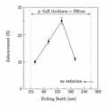
도 4는 도 3의 구조에서 광결정 깊이에 따른 광 추출효율을 나타내는 그래프이다.FIG. 4 is a graph showing light extraction efficiency according to photonic crystal depth in the structure of FIG. 3.
도 5는 반도체층의 두께가 한정된 경우 식각 깊이에 따른 광 추출효율을 나타내는 그래프이다.5 is a graph illustrating light extraction efficiency according to an etching depth when the thickness of a semiconductor layer is limited.
도 6 내지 도 8은 본 발명의 제1실시예를 나타내는 도로서,6 to 8 are diagrams showing a first embodiment of the present invention.
도 6은 본 발명의 제1실시예를 나타내는 단면도이다. 6 is a sectional view showing a first embodiment of the present invention.
도 7은 본 발명의 제1실시예에 따른 수평형 발광 소자의 일례를 나타내는 단면도이다. 7 is a cross-sectional view showing an example of a horizontal light emitting device according to the first embodiment of the present invention.
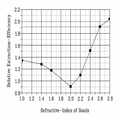
도 8은 광추출층의 굴절률에 따른 광 추출효율을 나타내는 그래프이다. 8 is a graph showing the light extraction efficiency according to the refractive index of the light extraction layer.
도 9 내지 도 13은 본 발명의 제2실시예를 나타내는 단면도이다.9 to 13 are cross-sectional views showing a second embodiment of the present invention.
도 9는 제2실시예에 따른 수평형 발광 소자 구조의 일례를 나타내는 단면도이다. 9 is a cross-sectional view showing an example of the structure of a horizontal light emitting device according to the second embodiment.
도 10은 제2실시예에 따른 수평형 발광 소자 구조의 다른 예를 나타내는 단면도이다. 10 is a cross-sectional view illustrating another example of a horizontal light emitting device structure according to the second embodiment.
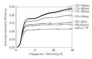
도 11은 투명 전도성층과 투명 금속층의 입사각에 따른 투과율을 나타내는 그래프이다.11 is a graph showing transmittance according to an incident angle of a transparent conductive layer and a transparent metal layer.
도 12는 투명 전도성층의 두께에 따른 광 추출효율을 나타내는 그래프이다.12 is a graph showing the light extraction efficiency according to the thickness of the transparent conductive layer.
도 13은 제2실시예에 의한 발광 소자를 나타내는 단면도이다.Fig. 13 is a sectional view showing a light emitting device according to the second embodiment.
도 14는 본 발명의 제3실시예를 나타내는 단면도이다.14 is a sectional view showing a third embodiment of the present invention.
<도면의 주요 부분에 대한 간단한 설명>BRIEF DESCRIPTION OF THE DRAWINGS FIG.
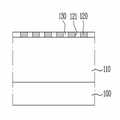
100, 200 : 기판 110, 210 : 반도체층100, 200:
120, 230 : 광추출층 130 : 투명 전도성 산화물120, 230: light extraction layer 130: transparent conductive oxide
220 : 투명 전도성층220: transparent conductive layer
본 발명은 질화물계 발광 소자 및 그 제조방법에 관한 것으로 특히, 발광 소자의 광 추출효율과 신뢰성을 향상시킬 수 있는 질화물계 발광 소자 및 그 제조방법에 관한 것이다.The present invention relates to a nitride-based light emitting device and a method of manufacturing the same, and more particularly to a nitride-based light emitting device and a method for manufacturing the light emitting device that can improve the light extraction efficiency and reliability.
발광 다이오드(Light Emitting Diode: LED)는 전류를 빛으로 변환시키는 잘 알려진 반도체 발광 소자로서, 1962년 GaAsP 화합물 반도체를 이용한 적색 LED가 상품화 된 것을 시작으로 GaP:N 계열의 녹색 LED와 함께 정보 통신기기를 비롯한 전자장치의 표시 화상용 광원으로 이용되어 왔다.Light Emitting Diodes (LEDs) are well-known semiconductor light emitting devices that convert current into light.In 1962, red LEDs using GaAsP compound semiconductors were commercialized, along with GaP: N series green LEDs. It has been used as a light source for display images of electronic devices, including.
이러한 LED에 의해 방출되는 광의 파장은 LED를 제조하는데 사용되는 반도체 재료에 따른다. 이는 방출된 광의 파장이 가전자대(valence band) 전자들과 전도대(conduction band) 전자들 사이의 에너지 차를 나타내는 반도체 재료의 밴드갭(band-gap)에 따르기 때문이다.The wavelength of the light emitted by these LEDs depends on the semiconductor material used to fabricate the LED. This is because the wavelength of the emitted light depends on the band gap of the semiconductor material, which represents the energy difference between the valence band electrons and the conduction band electrons.
질화 갈륨 화합물 반도체(Gallium Nitride: GaN)는 높은 열적 안정성과 폭넓은 밴드갭(0.8 ~ 6.2eV)을 가지고 있어, LED를 포함한 고출력 전자부품 소자 개발 분야에서 많은 주목을 받아왔다.Gallium nitride semiconductors (GaN) have high thermal stability and wide bandgap (0.8 to 6.2 eV), and have attracted much attention in the field of high output electronic component development including LEDs.
이에 대한 이유 중 하나는 GaN이 타 원소들(인듐(In), 알루미늄(Al) 등)과 조합되어 녹색, 청색 및 백색광을 방출하는 반도체 층들을 제조할 수 있기 때문이다.One reason for this is that GaN can be combined with other elements (indium (In), aluminum (Al), etc.) to produce semiconductor layers that emit green, blue and white light.
이와 같이 방출 파장을 조절할 수 있기 때문에 특정 장치 특성에 맞추어 재료의 특징들에 맞출 수 있다. 예를 들어, GaN를 이용하여 광기록에 유익한 청색 LED와 백열등을 대치할 수 있는 백색 LED를 만들 수 있다.Since the emission wavelength can be controlled in this manner, it can be tailored to the characteristics of the material according to the specific device characteristics. For example, GaN can be used to create a white LED that can replace the blue LEDs and incandescent lamps that are beneficial for optical recording.
이러한 GaN 계열 물질의 이점들로 인해, GaN 계열의 LED 시장이 급속히 성장하고 있다. 따라서, 1994년에 상업적으로 도입한 이래로 GaN 계열의 광전자장치 기술도 급격히 발달하였다.Due to the advantages of these GaN-based materials, the GaN-based LED market is growing rapidly. Therefore, since commercial introduction in 1994, GaN-based optoelectronic device technology has rapidly developed.
일반적으로, 반도체 발광 다이오드(LED)의 총 발광효율은 내부양자효율과 외부추출효율로 나눌 수 있다.In general, the total luminous efficiency of a semiconductor light emitting diode (LED) can be divided into internal quantum efficiency and external extraction efficiency.
내부양자효율은 LED 소자를 구성하는 물질의 특성과 관련된 양으로, 성장 과정 중에 발생하는 반도체 물질 내의 결함 여부와 전류 주입의 효율성 등에 의해 정해진다.The internal quantum efficiency is an amount related to the characteristics of the material constituting the LED device, and is determined by defects in the semiconductor material generated during the growth process and the efficiency of current injection.
이에 반해 외부추출효율은 반도체 내에서 생성된 빛이 실제로 관찰하고자 하는 외부 매질까지 빠져나오는 효율을 일컫는 것으로, 아무런 구조적 변화가 도입되지 않는 경우 단순히 반도체와 외부 매질 사이의 굴절률 차이로 결정된다.On the other hand, the external extraction efficiency refers to the efficiency in which the light generated in the semiconductor escapes to the external medium to be observed. If no structural change is introduced, the external extraction efficiency is simply determined as the difference in refractive index between the semiconductor and the external medium.
결과적으로, 반도체 LED의 총 발광효율은 내부양자효율과 외부추출효율의 곱으로 나타낼 수 있으며, 고효율 반도체 LED 개발을 위해서는 이 두 효율을 동시에 개선하는 노력이 필요하다.As a result, the total luminous efficiency of the semiconductor LED can be expressed as the product of the internal quantum efficiency and the external extraction efficiency. Efforts to improve these two efficiencies at the same time are needed to develop a high efficiency semiconductor LED.
본 발명이 이루고자 하는 기술적 과제는, 질화갈륨(GaN) 발광 소자에 광 추출효율 향상을 위한 광추출 구조를 도입함에 있어서, 전기적인 특성은 보존하면서, 광 추출효율을 개선할 수 있는 질화물계 발광 소자 및 그 제조방법을 제공하는 데 있다.The technical problem to be achieved by the present invention is a nitride-based light emitting device that can improve the light extraction efficiency while preserving electrical characteristics in introducing a light extraction structure for improving the light extraction efficiency to gallium nitride (GaN) light emitting device And to provide a method for producing the same.
상기 기술적 과제를 이루기 위해, 본 발명은, 질화물계 발광 소자에 있어서, 반도체층과; 상기 반도체층 상에 위치하며, 상기 반도체층과 굴절률이 같거나 상기 반도체층보다 굴절률이 큰 물질로 형성되는 광추출층을 포함하여 구성되는 것이 바람직하다.In order to achieve the above technical problem, the present invention is a nitride-based light emitting device, the semiconductor layer; Located on the semiconductor layer, preferably comprises a light extraction layer formed of a material having the same refractive index as the semiconductor layer or larger than the semiconductor layer.
상기 기술적 과제를 이루기 위한 다른 관점으로서, 본 발명은, 질화물계 발광 소자의 제조방법에 있어서, 반도체층을 형성하는 단계와; 상기 반도체층 상에 상기 반도체층과 굴절률이 같거나 상기 반도체층보다 굴절률이 큰 광추출층을 형성하는 단계와; 상기 광추출층을 식각하여 패턴을 형성하는 단계를 포함하여 구성되는 것이 바람직하다.As another aspect for achieving the above technical problem, the present invention, a method for manufacturing a nitride-based light emitting device, comprising the steps of forming a semiconductor layer; Forming a light extraction layer having the same refractive index as the semiconductor layer or having a larger refractive index than the semiconductor layer on the semiconductor layer; Etching the light extraction layer is preferably configured to include a step of forming a pattern.
이하, 첨부된 도면을 참고하여 본 발명에 의한 실시예를 상세히 설명하면 다음과 같다.Hereinafter, embodiments of the present invention will be described in detail with reference to the accompanying drawings.
본 발명이 여러 가지 수정 및 변형을 허용하면서도, 그 특정 실시예들이 도면들로 예시되어 나타내어지며, 이하에서 상세히 설명될 것이다. 그러나 본 발명을 개시된 특별한 형태로 한정하려는 의도는 아니며, 오히려 본 발명은 청구항들에 의해 정의된 본 발명의 사상과 합치되는 모든 수정, 균등 및 대용을 포함한다.While the invention is susceptible to various modifications and alternative forms, specific embodiments thereof are shown by way of example in the drawings and will herein be described in detail. Rather, the intention is not to limit the invention to the particular forms disclosed, but rather, the invention includes all modifications, equivalents and substitutions that are consistent with the spirit of the invention as defined by the claims.
동일한 참조번호는 도면의 설명을 통하여 동일한 요소를 나타낸다. 도면들에서 층들 및 영역들의 치수는 명료성을 위해 과장되어있다. 또한 여기에서 설명되는 각 실시예는 상보적인 도전형의 실시예를 포함한다.Like reference numerals denote like elements throughout the description of the drawings. In the drawings the dimensions of layers and regions are exaggerated for clarity. In addition, each embodiment described herein includes an embodiment of a complementary conductivity type.
층, 영역 또는 기판과 같은 요소가 다른 구성요소 "상(on)"에 존재하는 것으로 언급될 때, 이것은 직접적으로 다른 요소 상에 존재하거나 또는 그 사이에 중간 요소가 존재할 수도 있다는 것을 이해할 수 있을 것이다. 표면과 같은 구성 요소의 일부가 '내부(inner)'라고 표현된다면 이것은 그 요소의 다른 부분들 보다도 소자의 외측으로부터 더 멀리 있다는 것을 의미한다고 이해할 수 있을 것이다.It will be appreciated that when an element such as a layer, region or substrate is referred to as being present on another element "on," it may be directly on the other element or there may be an intermediate element in between . If a part of a component, such as a surface, is expressed as 'inner', it will be understood that this means that it is farther from the outside of the device than other parts of the element.
나아가 '아래(beneath)' 또는 '중첩(overlies)'과 같은 상대적인 용어는 여 기에서는 도면에서 도시된 바와 같이 기판 또는 기준층과 관련하여 한 층 또는 영역과 다른 층 또는 영역에 대한 한 층 또는 영역의 관계를 설명하기 위해 사용될 수 있다.Furthermore, relative terms such as "beneath" or "overlies" are used herein to refer to one layer or region relative to one layer or region and another layer or region with respect to the substrate or reference layer, as shown in the figures. Can be used to describe the relationship.
이러한 용어들은 도면들에서 묘사된 방향에 더하여 소자의 다른 방향들을 포함하려는 의도라는 것을 이해할 수 있을 것이다. 마지막으로 '직접(directly)'라는 용어는 중간에 개입되는 어떠한 요소가 없다는 것을 의미한다. 여기에서 사용되는 바와 같이 '및/또는'이라는 용어는 기록된 관련 항목 중의 하나 또는 그 이상의 어느 조합 및 모든 조합을 포함한다.It will be understood that these terms are intended to include other directions of the device in addition to the direction depicted in the figures. Finally, the term 'directly' means that there is no element in between. As used herein, the term 'and / or' includes any and all combinations of one or more of the recorded related items.
비록 제1, 제2 등의 용어가 여러 가지 요소들, 성분들, 영역들, 층들 및/또는 지역들을 설명하기 위해 사용될 수 있지만, 이러한 요소들, 성분들, 영역들, 층들 및/또는 지역들은 이러한 용어에 의해 한정되어서는 안 된다는 것을 이해할것이다.Although the terms first, second, etc. may be used to describe various elements, components, regions, layers, and / or regions, such elements, components, regions, layers, and / or regions It will be understood that it should not be limited by these terms.
이러한 용어들은 단지 다른 영역, 층 또는 지역으로부터 어느 하나의 요소, 성분, 영역, 층 또는 지역들을 구분하기 위해 사용되는 것이다. 따라서 아래에서 논의된 제1 영역, 층 또는 지역은 제2 영역, 층 또는 지역이라는 명칭으로 될 수 있다.These terms are only used to distinguish one element, component, region, layer or region from another region, layer or region. Thus, the first region, layer or region discussed below may be referred to as the second region, layer or region.
본 발명의 실시예들은 예를 들어, 사파이어(Al2O3)계 기판과 같은 비도전성 기판상에 형성된 질화갈륨(GaN)계 발광 소자를 참조하여 설명될 것이다. 그러나 본 발명은 이러한 구조에 한정되는 것은 아니다.Embodiments of the present invention will be described with reference to a gallium nitride (GaN) based light emitting device formed on a nonconductive substrate such as, for example, a sapphire (Al2 O3 ) based substrate. However, the present invention is not limited to this structure.
본 발명의 실시예들은 도전성 기판을 포함하여 다른 기판을 사용할 수 있다. 따라서 GaP 기판상의 AlGaInP 다이오드, SiC 기판상의 GaN 다이오드, SiC 기판상의 SiC 다이오드, 사파이어 기판상의 SiC 다이오드, 및/또는 GaN, SiC, AlN, ZnO 및/또는 다른 기판상의 질화물계 다이오드 등의 조합이 포함될 수 있다. 더구나 본 발명은 활성영역은 다이오드 영역의 사용에 한정되는 것은 아니다. 또한 활성영역의 다른 형태들이 본 발명의 일부 실시예들에 따라서 사용될 수도 있다.Embodiments of the invention may use other substrates, including conductive substrates. Thus, combinations of AlGaInP diodes on GaP substrates, GaN diodes on SiC substrates, SiC diodes on SiC substrates, SiC diodes on sapphire substrates, and / or GaN, SiC, AlN, ZnO and / or nitride based diodes on other substrates may be included. have. Moreover, the present invention is not limited to the use of the diode region. Other forms of active area may also be used in accordance with some embodiments of the present invention.
반도체 발광 소자(LED)의 추출효율은 빛이 발생하는 반도체 발광층과 최종적으로 빛을 관측하는 매질(공기 또는 에폭시) 사이의 굴절률 차이에 의하여 결정된다. 반도체 매질은 통상적으로 높은 굴절률(n > 2)을 가지므로, 광 추출효율은 대개 수 %에 지나지 않는다.The extraction efficiency of the semiconductor light emitting device (LED) is determined by the difference in refractive index between the semiconductor light emitting layer in which light is generated and the medium (air or epoxy) that finally observes the light. Since the semiconductor medium typically has a high refractive index (n> 2), the light extraction efficiency is usually only a few%.
예를 들어, 질화갈륨(n = 2.4) 기반의 청색 발광 소자의 경우, 외부 물질을 에폭시(n = 1.4)로 가정했을 때 발광 소자의 상층부를 통한 광 추출효율은 약 9% 정도에 불과하다. 이를 제외한 나머지 빛들은, 소자 내부에 전반사 과정에 의해 갇혀 있으면서, 양자우물 층과 같은 흡수층에 의해 소실된다.For example, in the case of a blue light emitting device based on gallium nitride (n = 2.4), light extraction efficiency through the upper layer of the light emitting device is only about 9% when an external substance is assumed to be epoxy (n = 1.4). The rest of the light is trapped by the total reflection process inside the device, and is lost by an absorbing layer such as a quantum well layer.
이러한 반도체 발광 소자의 추출효율을 개선하기 위해서는 전반사 과정을 겪는 빛들을 외부로 추출할 수 있도록 구조를 변형해야 한다. 이러한 구조 변형 중 가장 단순한 방안은 굴절률이 높은 물질로 이루어진 반구(hemisphere)를 발광 소자 상층부에 덧씌우는 것이다.In order to improve the extraction efficiency of the semiconductor light emitting device, the structure must be modified to extract the light that undergoes total reflection. The simplest of these structural modifications is to overlay a hemisphere made of a material with high refractive index on the upper layer of the light emitting device.
입사각은 빛과 입사면 사이의 각이므로, 반구의 각 점에서는 입사각이 항상 수직이다. 굴절률이 다른 두 매질 사이의 투과율은 입사각이 수직일 때 가장 높으 며, 모든 방향에 대해 전반사 각도는 더 이상 존재하지 않게 된다.Since the angle of incidence is the angle between the light and the incident surface, the angle of incidence at each point of the hemisphere is always perpendicular. The transmission between two media with different refractive indices is highest when the angle of incidence is perpendicular, and the total reflection angle no longer exists for all directions.
실제로, 반도체 발광 소자의 경우, 에폭시로 이루어진 반구를 씌우게 되는데, 이는 표면 보호의 역할뿐만 아니라 추출효율 향상에도 기여한다.In fact, in the case of a semiconductor light emitting device, hemispheres made of epoxy are covered, which contributes not only to surface protection but also to improving extraction efficiency.
이러한 효과를 더 극명하게 이용하는 방법은, 도 1에서와 같이, 에폭시 층(1)과 반도체 소자(2) 사이에 굴절률이 반도체와 유사한 반구(3)를 추가적으로 도입하는 것이다. 이 경우, 도 2에서 도시하는 바와 같이, 추가로 도입한 반구의 굴절률이 반도체의 굴절률에 접근할수록 추출효율은 점점 증가한다.A further advantage of this effect is the introduction of a hemisphere 3 with a similar refractive index to the semiconductor between the epoxy layer 1 and the
이는 반도체 소자와 추가로 도입한 반구 사이의 임계각이 커졌기 때문이다. 가시광선 영역에서 흡수가 없고, 투명한 물질의 한 예로 TiO2를 제안할 수 있다. 가령, 이 물질로 이루어진 반구를 적색 발광 소자에 적용한다고 가정했을 때, 이론적으로 기존대비 약 3배 이상의 추출효율 향상을 얻을 수 있다.This is because the critical angle between the semiconductor element and the additional introduced hemisphere is increased. As an example of a transparent material having no absorption in the visible light region, TiO2 may be proposed. For example, assuming that a hemisphere made of this material is applied to a red light emitting device, it is theoretically possible to obtain an extraction efficiency improvement of about 3 times or more.
굴절률이 높은 반구를 추가적으로 도입하는 방법은, 단순하면서도 아주 효과적인 방법이다. 그러나 이러한 방법을 적용하기 위해서는 높은 굴절률을 가지면서, 동시에 빛의 발광 파장 영역에서 흡수가 없는 투명한 물질을 찾아야 한다.The introduction of hemispheres with high refractive indices is a simple and very effective method. However, in order to apply such a method, a transparent material having high refractive index and no absorption in the emission wavelength range of light must be found.
또한, 발광 소자를 충분히 덮을 수 있는 만큼의 크기를 가진 반구를 제작하고, 이 반구를 부착하는 작업은 난제가 될 수 있다.In addition, the operation of manufacturing a hemisphere having a size sufficient to cover the light emitting element, and attaching the hemisphere may be a challenge.
외부 광 추출효율을 개선하는 다른 방법으로는, 발광 구조의 측면을 역 피라미드 모양으로 변형하는 것을 들 수 있다. 이는 발광 소자 내에서 전반사 되면서 옆으로 진행하는 빛이 피라미드 면에서 반사되어 상층부로 나오게 되는 원리를 따 른다.Another method of improving the external light extraction efficiency is to deform the side of the light emitting structure into an inverted pyramid shape. This is based on the principle that the light propagating sideways while being totally reflected in the light emitting device is reflected from the pyramid plane and comes out to the upper layer.
그러나 이러한 방법은 소자의 크기가 커질수록 향상 효과가 감소하는 단점이 있다. 이는 빛이 옆으로 진행하면서 필연적으로 동반되는 흡수 손실 때문이다. 따라서 흡수가 있는 실제 구조에서 높은 향상효과를 얻기 위해서는, 빛이 되도록 짧은 경로를 겪은 뒤 외부로 방출되는 것이 중요하다.However, this method has a disadvantage in that the improvement effect decreases as the size of the device increases. This is due to the absorption loss inevitably accompanied by the light traveling sideways. Therefore, in order to obtain a high enhancement effect in the actual structure with absorption, it is important to go to the outside after a short path to light.
이를 위해 전반사 조건을 완화할 수 있는 구조를 발광 소자 내에 도입하는 연구들이 진행되었다. 대표적으로 발광 소자 구조를 공진기 형태로 설계하여 초기부터 특정 방향의 출력을 이끄는 방법, 수 마이크론 크기 이상의 반구형 렌즈를 상층부에 배열하여 임계각을 크게 하는 방법을 들 수 있다.To this end, studies have been conducted to introduce a structure into the light emitting device that can alleviate the total reflection condition. Typically, a light emitting device structure is designed in the form of a resonator to drive output in a specific direction from the beginning, and a method of increasing a critical angle by arranging a hemispherical lens of several microns or more in an upper layer.
그러나 이러한 방법들은 제작상의 난점 등으로 인해 실용화에 이르지는 못하고 있다. 또 다른 방법으로, 발광 소자 출력 부에 빛의 파장 정도의 크기에 해당하는 거친 면을 도입하여 산란 과정을 통해 추출효율을 증대하는 방법이 있다.However, these methods have not been brought to practical use due to manufacturing difficulties. As another method, there is a method of increasing extraction efficiency through a scattering process by introducing a rough surface corresponding to the size of the wavelength of light to the light emitting device output unit.
발광 소자 상층 부에 거친 면을 형성하는 방법은 각 발광 소자를 이루는 물질에 따라 여러 가지 화학적인 공정이 개발되어 있다. 빛이 거친 표면을 만나게 되면 전반사에 해당하는 입사 각도라도 그 중 일부는 투과할 수 있다.In the method of forming the rough surface on the upper portion of the light emitting device, various chemical processes have been developed depending on the material of each light emitting device. When light meets a rough surface, some of the light may pass through even the incident angle corresponding to total reflection.
그러나 한 번의 산란에 의한 투과율은 그리 크지 않으므로, 높은 추출효과를 기대하기 위해서는 같은 산란 과정을 반복적으로 겪어야 한다. 따라서, 발광 소자 내에 흡수가 큰 구성 물질이 존재하는 경우, 거친 면에 의한 추출효율 향상은 그리 효과적이지 않다.However, the transmission by one scattering is not so large, so the same scattering process must be repeated repeatedly in order to expect a high extraction effect. Therefore, when there is a constituent material having a high absorption in the light emitting device, the extraction efficiency improvement by the rough surface is not very effective.
이와 비교하여, 공간적으로 주기적인 굴절률의 배치를 가지는 광결정을 도입 하게 되면, 상대적으로 크게 추출효율을 개선할 수 있다. 또한, 적절한 광결정 주기를 선택하게 되면, 발광 소자 출력의 방향성을 조절할 수 있다. 발광 소자의 응용 분야에 따라 의미 있는 시야 각이 다르므로, 각 용도에 어울리는 방향성을 설계하는 것은 중요한 작업이라 할 수 있다.In comparison, when a photonic crystal having a spatially periodic refractive index arrangement is introduced, the extraction efficiency can be improved relatively large. In addition, when the appropriate photonic crystal period is selected, the directivity of the light emitting device output can be adjusted. Since a meaningful viewing angle varies depending on the application field of the light emitting device, it is important to design a directionality suitable for each application.
대면적의 광결정 구현은 홀로그램 식각(holography lithography), 자외선 광 식각(UV photolithography), 나노 임프린트 식각(Nano-imprinted lithography) 등을 활용할 수 있으므로, 실용화에도 용이한 기술이라 할 수 있다.Large-area photonic crystals can be used for holographic lithography, ultraviolet photolithography, nano-imprinted lithography, and the like.
광결정을 통한 발광 소자의 광 추출효율 개선을 위한 노력은 광결정을 이용하여 자발 방출률을 조절할 수 있다는 연구에서 출발한다.Efforts to improve the light extraction efficiency of the light emitting device through the photonic crystal start from the study that the spontaneous emission rate can be controlled by using the photonic crystal.
이후, 광결정이 발광 소자의 추출효율 향상에 기여한다는 것을 분산특성 곡선을 활용해 이론적으로 증명되었고, 광결정이 추출효율 향상에 기여하는 과정은 크게 두 가지로 요약될 수 있다.Thereafter, it has been theoretically proved that the photonic crystal contributes to the extraction efficiency of the light emitting device by using the dispersion characteristic curve, and the process of the photonic crystal to the extraction efficiency can be summarized into two ways.
하나는 광 밴드갭(photonic band-gap) 효과를 이용해 평면 방향의 빛 이동을 차단하여 수직 방향으로 추출하는 것이고, 다른 하나는 분산곡선에서 라이트 콘(light cone) 바깥에 위치한 상태밀도가 높은 모드와 결합하여 외부로 추출하는 것이다.One is to extract light in the vertical direction by blocking the light movement in the planar direction by using the photonic band-gap effect. The other is a state density mode that is located outside the light cone in the dispersion curve. Combine and extract to the outside.
이러한 두 가지 원리는 광결정의 주기에 따라 독립적으로 적용될 수 있다. 하지만, 광 밴드갭 거울 효과나 분산곡선의 상태밀도가 잘 정의되기 위해서는, 반 파장 정도의 두께를 가지는 얇은 박막이 상하로 높은 굴절률 대비가 있는 상황에서 광결정을 형성할 때 가능하다.These two principles can be applied independently depending on the period of the photonic crystal. However, in order to define the optical band gap mirror effect or the state density of the dispersion curve well, it is possible to form a photonic crystal in a situation where a thin film having a thickness of about half wavelength has a high refractive index contrast up and down.
더군다나, 광결정의 공기 구멍이 발광층을 관통하기 때문에 필연적으로 이득 매질의 손실을 가져오며, 추가적으로 표면 비발광 결합에 의한 내부양자효율의 감소를 피할 수 없다.Furthermore, since the air hole of the photonic crystal penetrates the light emitting layer, it inevitably leads to a loss of the gain medium, and further reduction of the internal quantum efficiency due to surface non-emitting coupling is inevitable.
광 밴드갭 거울 효과나 강한 분산 특성은 일반적인 발광 소자 구조에서는 구현하기 어렵기 때문에 특수한 경우에만 적용되는 방법이라 할 수 있다. 이 문제를 해결하기 위해서는, 발광 소자의 능동매질을 포함하지 않고, 표면에 국한해서 광결정을 제작하여야 한다.Since the optical bandgap mirror effect or the strong dispersion property is difficult to implement in a general light emitting device structure, it can be said to be applied only in a special case. In order to solve this problem, the photonic crystal should be fabricated only on the surface without including the active medium of the light emitting device.
이 경우, 높은 굴절률 대비가 있는 박막에 광결정을 도입할 때처럼 강한 분산 특성을 활용할 수는 없지만, 일반적인 회절 이론에 따라 전반사에 해당하는 빛이 주기적인 구조와 결합하여 외부로 추출될 수 있다.In this case, strong dispersion characteristics cannot be utilized as in the case of introducing a photonic crystal into a thin film having a high refractive index contrast, but according to general diffraction theory, light corresponding to total reflection can be extracted to the outside in combination with a periodic structure.
현재 광결정과 반도체층의 발광층을 공간적으로 분리하여, 발광층의 특성을 저하시키지 않으면서 추출효율을 개선하고자 하는 노력이 활발하게 진행되고 있다.At present, efforts have been actively made to improve the extraction efficiency by spatially separating the photonic crystal and the light emitting layer of the semiconductor layer without degrading the characteristics of the light emitting layer.
같은 방법으로, InGaAs 양자우물을 채택한 발광 소자 구조에 대해서도 추출효율 향상을 꾀한 예가 있으며, 유기 발광 소자에서 유리 기판 상에 형성된 광결정을 이용하여 외부 광추출 효율을 1.5배 이상 끌어올린 결과가 보고되기도 하였다.In the same way, there is an example in which the extraction efficiency is improved for the light emitting device structure adopting InGaAs quantum well, and the result of increasing the external light extraction efficiency by 1.5 times or more by using the photonic crystal formed on the glass substrate in the organic light emitting device has been reported. .
앞에서 언급한 바와 같이, 주기적인 광결정 구조를 표면에 도입하여 전반사에 의해 갇혀있는 빛을 회절 과정을 통해 추출하는 방법도 시도되었다. 가령, 200nm 정도의 주기를 가지는 광결정을 p-형 GaN 반도체 표면에 형성하여 추출효율이 증가된 것이 보고되었다.As mentioned above, a method of extracting light trapped by total reflection by introducing a periodic photonic crystal structure to the surface has been attempted. For example, it has been reported that the extraction efficiency is increased by forming a photonic crystal having a period of about 200 nm on the p-type GaN semiconductor surface.
이 외에, GaN 계열 발광 소자의 능동매질 영역까지 광결정을 제작한 뒤, 광 밴드갭 효과를 이용하여 높은 추출효율 향상 효과를 보고한 연구도 있었지만, 입력 전류가 증가하면 추출효율이 낮아지는 단점이 있다. 이는 앞서 지적한 대로, 발광층까지 식각하여 광결정을 도입하게 되면, 특히, 전류-전압 특성이 저하되기 때문이다.In addition, there has been a study that reports a high extraction efficiency improvement effect using the optical band gap effect after fabricating the photonic crystal to the active medium region of the GaN series light emitting device, but the extraction efficiency is lowered as the input current increases . This is because, as pointed out above, when the photonic crystal is introduced by etching the light emitting layer, in particular, the current-voltage characteristic is degraded.
이상을 종합해 볼 때 발광 소자의 외부 광 추출효율을 개선 원리는 구조의 변형을 통해 전반사 조건을 완화하는 방법, 표면에 거친 면을 도입하는 방법, 굴절률 대비가 큰 박막 내에 광결정을 형성하여 광 밴드갭 효과를 이용하는 방법, 광결정과 발광층을 분리하여 전반사에 의해 갇혀있는 빛을 회절 과정을 통해 외부로 추출하는 방법 등으로 요약할 수 있다.In summary, the principle of improving the external light extraction efficiency of the light emitting device is to reduce the total reflection condition by modifying the structure, to introduce a rough surface on the surface, and to form a photonic crystal in a thin film having a large refractive index contrast to the optical band. It can be summarized as a method using a gap effect, a method of separating the photonic crystal and the light emitting layer and extracting the light trapped by total reflection to the outside through a diffraction process.
이 중 발광 소자의 구조의 현실성과 효율의 증대성을 감안할 때, 발광 소자 표면에 주기적인 광결정 구조를 도입하여 추출효율을 개선하는 방법이 가장 우수하다고 할 수 있다.Among these, considering the reality of the structure of the light emitting device and the increase in efficiency, it can be said that the method of improving the extraction efficiency by introducing a periodic photonic crystal structure on the surface of the light emitting device.
도 3에서 도시하는 바와 같은 수평형 GaN 계열 발광 소자는 GaN에 비해 굴절률이 상대적으로 낮은 사파이어(n = 1.76) 기판(10) 위에 성장한 구조이다. GaN 반도체층(20)의 전체 두께는 약 5㎛에 이르므로, 다양한 고차 모드가 존재하는 도파로 구조로 간주할 수 있다. GaN 반도체층(20)의 상층부는 p-형 GaN 반도체층(21)부터 출발하며, 그 아래에 발광층(22) 영역에 해당하는 다중양자우물 층이 위치한다.As shown in FIG. 3, the horizontal GaN series light emitting device has a structure grown on a sapphire (n = 1.76)
이러한 발광층(22)의 하측에는 n-형 GaN 반도체층(23)이 위치하며, 이 n-형 GaN 반도체층(23)과 기판(10) 사이에는 버퍼층(24)이 위치할 수 있다. 또한, 기판(10)의 반대측에는 반사막(50)을 형성할 수 있다.An n-type
수평형 GaN 계열 발광 소자는 전체 면적에 걸쳐 고르게 전류를 공급하기 위해, 대개 ITO와 같은 투명전극층(30)을 p-형 GaN 반도체층(21) 위에 증착한다. 따라서, 수평형 GaN 계열 발광 소자에 광결정(40)을 도입할 때, 식각할 수 있는 최대 범위는 투명전극층(30) 두께와 p-형 GaN 반도체층(21)의 두께를 합한 값이 된다. 일반적으로, 이러한 투명전극층(30)과 p-형 GaN 반도체층(21)의 두께는 100 ~ 300nm 사이이다.In the horizontal GaN series light emitting device, a
우선, 광결정(40) 식각 깊이에 따라 추출효율이 변화하는 양상을 살펴보기 위해, 컴퓨터 전산모사(3D-FDTD) 계산을 실시한 결과를 살펴보면, 도 4에서와 같이, 두 가지 특이 사항을 발견할 수 있다.First, in order to examine the extraction efficiency changes according to the etching depth of the
첫 번째, 추출효율은 광결정(40) 식각 깊이에 비례하여 서서히 증가하다가, GaN 반도체층(20)을 식각하는 부분부터 다시 크게 늘어난다. 두 번째, 어느 정도 이상의 식각 깊이에 대해 추출효율은 더 이상 증가하지 않고, 포화되는 경향을 나타낸다.First, the extraction efficiency gradually increases in proportion to the etching depth of the
이 두 가지 사항을 종합하면, 최대의 추출효율을 얻기 위해서는 GaN 반도체층(20)을 포함하는 영역을 어느 정도 이상의 식각 깊이를 지닌 광결정(40)을 도입하는 것이 필수적일 수 있다.Putting these two points together, in order to obtain the maximum extraction efficiency, it may be necessary to introduce the
이때, 추출효율이 포화되는 시점의 식각 깊이와 일반적인 p-형 GaN 반도체층(21)의 두께가 거의 비슷하므로, 발광층(22) 영역을 식각하지 않고, 이론적인 추출효율의 포화값에 도달하는 것이 가능하다.At this time, since the etch depth at the time when the extraction efficiency is saturated and the thickness of the general p-type
그러나 실제 실험에서는 광결정(40)의 식각 깊이에 대해 광 출력을 조사하 면, 도 5에서와 같이, 특정 깊이 이상 p-형 GaN 반도체층(21)을 식각하게 되었을 때, 오히려 광 출력이 줄어드는 현상이 발견된다.However, in the actual experiment, when the light output is irradiated with respect to the etching depth of the
이와 같이 발광층(22)인 양자우물구조가 아직 노출되지 않았음에도 광 출력이 감소하는 이유는 p-형 GaN 반도체층(21)의 부피 감소로 인해 저항이 증가하였기 때문이다. 저항 증가는 고출력 발광 소자를 요구하는 응용 분야일수록 더욱 문제가 될 수 있다.The reason why the light output is reduced even though the quantum well structure, which is the light emitting layer 22, is not yet exposed is that the resistance is increased due to the volume reduction of the p-type
즉, 현재의 광결정을 가지는 발광 소자의 구조는 저항 증가 문제로 인해 광학적인 관점에서 추출효율이 최대가 되는 식각 깊이를 이용하지 못하고 있다. 따라서, 해결되어야 할 사항은 저항 증가의 문제를 야기하지 않으면서, 광결정에 의한 추출효율이 최대가 되는 식각 깊이를 적용할 수 있는 새로운 구조를 개발하는 것이다.That is, the current structure of the light emitting device having a photonic crystal does not use the etching depth, the maximum extraction efficiency from the optical point of view due to the problem of resistance increase. Therefore, the problem to be solved is to develop a new structure that can apply the etch depth is the maximum extraction efficiency by the photonic crystal without causing the problem of resistance increase.
상술한 전산모사를 통해 도출하였던 식각 깊이에 대한 추출효율 변화를 수록한 그래프를 살펴보면, 새로운 구조에 대한 하나의 단초를 얻을 수 있다. 그래프에서 발견했던 특이 사항 중의 하나는 광결정(40)의 식각 깊이가 ITO 투명전극층(30)에서 GaN 반도체층(20)으로 넘어갈 때, 추출효율이 눈에 띄게 상승한다는 점이다.Looking at the graph containing the extraction efficiency change with respect to the etching depth derived through the computer simulation described above, one step for the new structure can be obtained. One of the peculiarities found in the graph is that when the etch depth of the
그 이유는 기본적으로 ITO의 굴절률(n = 1.8)이 GaN 반도체층(20)보다 작기 때문이다. 즉, 굴절률이 작은 영역 내에 광결정(40)을 도입하는 것은 추출효율 개선에 큰 도움을 주지 못한다. 이는 광결정(40)이 전반사 과정을 일으키는 빛을 추출하는 역할을 수행한다는 점을 상기하면 이해할 수 있다.This is because the refractive index (n = 1.8) of ITO is basically smaller than that of the
추출효율 정도는 결국 빛이 얼마나 광결정(40) 영역을 느낄 수 있는 지에 달 려 있다. 일반적으로, 전반사 현상이 일어날 때, 굴절률이 다른 두 면 사이에는 표면감쇠파가 발생한다. 표면감쇠파는 두 경계면의 표면을 따라 존재하며, 경계면의 수직방향에 대해 그 크기가 지수적으로 감소하는 특성을 가진다.The degree of extraction efficiency depends on how light can feel the
가령, ITO 층만을 식각한 경우, 전반사에 해당하는 빛은 ITO 투명전극층(30) 내에 형성되어있는 광결정(40)을 단지 표면감쇠파의 크기만큼만 인지할 수 있다. 따라서, 그리 큰 추출효율 향상은 기대할 수 없다.For example, when only the ITO layer is etched, light corresponding to total reflection can recognize the
결론적으로, 광결정(40)을 통하여 보다 많은 양의 빛을 추출하기 위해서는 광결정(40)과 빛의 강한 상호 작용이 요구되며, 물리적으로는 GaN 계열 발광 소자 내에 형성된 전반사 모드와 광결정(40) 구조 사이의 공간적인 겹침이 주요한 인자가 된다. 즉, 전반사 과정 중에 발생하는 표면감쇠파를 교란하기 위해서는 광결정(40) 형성을 위해 GaN 반도체층(20)을 식각하는 것이 필수적일 수 있다.In conclusion, in order to extract a greater amount of light through the
그런데 GaN 반도체층을 식각한다는 것을 다른 의미로 풀이하면, GaN 반도체층과 유사하거나 더 큰 굴절률을 가진 물질을 식각한다는 뜻이 된다. 즉, p-형 GaN 반도체층 위에 굴절률이 유사한 물질을 증착한 뒤, 광결정(40)을 형성하면, p-형 GaN 반도체층을 식각하지 않아도 추출효율 면에서 유사한 효과를 기대할 수 있다.In other words, the etching of the GaN semiconductor layer may be interpreted to mean that a material having a refractive index similar to or greater than that of the GaN semiconductor layer is etched. That is, when the
그리고 새롭게 증착하는 물질이 만약 GaN보다 굴절률이 더 큰 물질이라면, 상술한 광결정 효과보다 더 우수한 성질을 나타낼 수 있다. 그 이유는 광결정의 효과가 기본적으로 구조를 구성하고 있는 두 물질의 굴절률 차이에 의해 좌우되기 때문이다.In addition, if the newly deposited material has a larger refractive index than GaN, it may exhibit better properties than the above-described photonic crystal effect. This is because the effect of the photonic crystal is basically dependent on the refractive index difference between the two materials constituting the structure.
따라서 질화갈륨(GaN) 발광 소자에 광 추출효율 향상을 위한 광추출 구조를 도입함에 있어서, 최상층의 질화갈륨 반도체층(보통, p-GaN)을 식각하는 대신, 질화갈륨 반도체층 상부에 추가로 도입한 물질 내에 광결정(photonic-crystal)과 같은 광 추출구조를 형성함으로써, 전기적인 특성은 보존하면서, 광 추출효율을 개선할 수 있다.Therefore, in introducing a light extraction structure for improving light extraction efficiency to the gallium nitride (GaN) light emitting device, instead of etching the gallium nitride semiconductor layer (usually p-GaN) of the uppermost layer, it is additionally introduced above the gallium nitride semiconductor layer By forming a light extraction structure such as a photonic-crystal in a material, it is possible to improve the light extraction efficiency while preserving the electrical properties.
이와 같이, 질화갈륨 반도체층 상에 광 추출구조를 형성하는 실시예는 다음과 같다.Thus, an embodiment of forming the light extraction structure on the gallium nitride semiconductor layer is as follows.
<제1실시예>≪ Embodiment 1 >
먼저, 도 6에서 도시하는 바와 같이, 기판(100) 상에 질화갈륨(GaN) 계열 반도체층(110)이 형성된 상태에서, 이 반도체층(110) 상에 반도체층(110)과 굴절률이 유사하거나 더 큰 물질을 이용하여 광추출층(120)이 형성된다.First, as shown in FIG. 6, in the state in which a gallium nitride (GaN) -based
이러한 광추출층(120)은 특정 패턴을 이룰 수 있으며, 이러한 특정 패턴은 주기적인 구조를 가지는 광결정을 이루도록 할 수 있다. 이와 같은 광결정의 형성은 식각 또는 기타 패터닝 방법을 통하여 이루어질 수 있다.The
이러한 광결정 구조의 형성은, 홀(121)을 형성하는 포지티브 리소그래피(positive lithography)와, 기둥 구조(rod)를 형성하는 네가티브 리소그래피(negative lithography)가 모두 적용 가능하다.For the formation of the photonic crystal structure, both positive lithography forming the
즉, 광추출층(120)을 증착하여 형성한 후에 리소그래피와 식각 과정으로 광결정 패턴을 형성할 수 있고, 반대로, 반도체층(110) 상에서 리소그래피를 수행한 후에 광추출층(120)을 증착하고, 이후에 리프트 오프(lift off) 과정을 통하여 패턴을 형성할 수도 있다.That is, after the
이와 같이 주기적인 광결정 구조가 발광 소자의 표면에 위치하게 되면 전반사에 의해 갇혀있는 빛을 회절 과정을 통해 추출할 수 있어 광 추출효율이 향상될 수 있다. 그러나 이러한 광추출층(120)이 특정 패턴을 가지지 않아도 표면거칠기 형성 등에 의하여 광 추출효율은 향상될 수 있다.When the periodic photonic crystal structure is located on the surface of the light emitting device, light trapped by total reflection can be extracted through a diffraction process, thereby improving light extraction efficiency. However, even if the
이때, 광추출층(120)에 광결정의 형성을 위한 홀(121)에 투명전극 물질이 형성될 수 있으며, 이러한 투명전극 물질은 투명 전도성 산화물(Tansparent Conducting Oxide; TCO; 130)이 이용될 수 있다.In this case, the transparent electrode material may be formed in the
이러한 투명 전도성 산화물(130)로는 ITO(Indium-Tin-Oxide)가 이용될 수 있으며, 기타 IZO(Indium-Zinc-Oxide), AZO(Aluminum-Zinc-Oxide), MZO(Magnesium-Zinc-Oxide), 또는 GZO(Gallium-Zinc-Oxide) 등의 물질이 이용될 수도 있다.ITO (Indium-Tin-Oxide) may be used as the transparent
반도체층(110)이 질화갈륨층일 경우 질화갈륨의 굴절률이 2.4이므로 광추출층(120)의 굴절률은 대략 2.4이거나 그보다 클 수 있다. 이러한 광추출층(120)의 굴절률은 2.4보다 약간 작을 수도 있다.When the
또한, 이러한 광추출층(120)은 산화물 또는 질화물이 이용될 수 있으며, 특히, SiN 또는 TiO2가 이용될 수 있다.In addition, the
도 7은 이러한 광추출층(120)을 가지는 수평형 발광 소자의 구조를 나타내고 있으며, 반도체층(110)은 굴절률이 1.78인 사파이어 기판(100) 상에 순차적으로 형성되는 n-형 반도체층(111)과, 활성층(112), 및 p-형 반도체층(113)으로 이루어질 수 있다. 경우에 따라, 상기 n-형 반도체층(111)은 버퍼층(114) 상에 형성될 수 있 다.7 illustrates a structure of a horizontal light emitting device having the
이때, 상기 광추출층(120)과 인접하는 p-형 반도체층(113)은 광추출층(120)의 패턴 형성시에 식각되지 않고, p-형 반도체층(113)은 전체적으로 그 적층시의 두께가 유지될 수 있다. 이러한 p-형 반도체층(113)의 두께는 30 내지 500nm가 될 수 있다. 또한, 광추출층(120)의 두께는 150nm 이상일 수 있다.At this time, the p-
도 7에서 광추출층(120)의 패턴은 확대되어 표현되어 있다. 이러한 광추출층(120)의 패턴은 GaN 반도체에서 광결정을 이룰 수 있도록 하는 다수의 홀(121)로 이루어지고, 이러한 홀(121)의 반경, 깊이, 및 주기는 해당 반도체층(110)에 최적화될 수 있다.In FIG. 7, the pattern of the
즉, 홀(121)과 홀(121) 사이의 간격인 주기를 a라 할 때, 홀(121)의 반경은 0.10a 내지 0.45a가 될 수 있고, 홀(121)의 깊이는 0.25λ/n 내지 10λ/n일 수 있다. 여기서, λ는 발광되는 빛의 파장이고, n은 광결정이 형성되는 매질, 즉, p-형 반도체층(113)의 굴절률이다. 또한, 주기(a)는 200nm 내지 5000nm가 될 수 있다.That is, when a period that is an interval between the
한편, 상술한 바와 같이, 이와 같이 홀(121)을 형성하는 대신에, 규칙적인 기둥 구조를 형성하여도 광결정 구조를 형성할 수 있다.On the other hand, as described above, instead of forming the
이때, n-형 반도체층(111) 상에 n-형 전극(140)이 이루어지도록 하기 위하여 n-형 반도체층(111)이 드러나도록 일측이 식각될 수 있고, 광추출층(120)이 형성된 부분의 상측에는 p-형 전극(150)이 형성될 수 있다.At this time, one side may be etched to expose the n-
이와 같은 광추출층(120)을 이루는 물질의 두께를 자유롭게 결정될 수 있고, 이와 같이, 고 굴절률의 물질을 증착하여 광결정을 형성하는 구조는 적색, 녹색 및 기타 다른 색을 발광하는 모든 발광 소자 구조에 적용이 가능하다.The thickness of the material forming the
본 발명의 효과를 살펴보기 위해, 도 8에서 도시하는 바와 같이, 제1실시예의 구조에 대하여 광추출층(120)의 굴절률에 따른 추출효율의 변화를 조사하였다.In order to examine the effects of the present invention, as shown in FIG. 8, the variation of extraction efficiency according to the refractive index of the
도 8의 그래프에서 수직축은 광 추출구조를 도입하지 않은 일반적인 평면 구조에 대한 상대적인 광 추출효율 증대비를 표시한 것이다.In the graph of FIG. 8, the vertical axis represents a ratio of increasing light extraction efficiency relative to a general planar structure without introducing a light extraction structure.
이 결과를 살펴보면, 투명 전도성 산화물(130)의 굴절률과 광추출층(120)의 굴절률 차이가 커질수록 광 추출효율 증대비가 상승함을 알 수 있다. 여기서 점선은 반도체층의 최상층(이 경우 p-형 반도체층)을 식각하여 광결정을 형성한 경우의 광 추출효율을 나타낸다.Looking at the results, it can be seen that the light extraction efficiency increase ratio increases as the difference between the refractive index of the transparent
그리고, 광추출층(120)의 굴절률이 2.6 근처일 때, p-형 GaN 반도체층을 식각한 것과 유사한 광 추출효율 증대효과를 나타낸다. 이때, 굴절률이 더 큰 물질을 도입하여 광추출층(120) 또는 광결정을 형성하면, p-형 반도체층을 식각하여 광결정을 형성하는 상술한 광결정 구조보다 우수한 광 추출효율 향상 효과가 나타나기 시작한다.In addition, when the refractive index of the
따라서, 상기 광추출층(120)이 갖추어야 할 조건은 상술한 바와 같이, 굴절률이 반도체층(20)의 굴절률(2.4)과 유사하거나 그보다 커야 하며, 그 두께는 최소 150nm(λ/n) 이상일 수 있다. 경우에 따라서는 최소 λ/4n의 두께일 수 있다.Therefore, as described above, the
또한, 이러한 광추출층(120)을 이루는 물질은 발광 소자의 발광층의 파장 영역 내에 흡수 손실이 존재해서는 안 되며, 투명 전도성 산화물(130)과 물리적인 접합력이 뛰어나야 한다.In addition, the material constituting the
이러한 조건을 만족하는 물질로는 상술한 바와 같이, 굴절률이 대략 2.4인 실리콘 질화물(Si3N4) 또는 굴절률이 3.0인 티타늄 산화물(TiO2)이 바람직하다.As the material satisfying such a condition, as described above, silicon nitride (Si3 N4 ) having a refractive index of about 2.4 or titanium oxide (TiO2 ) having a refractive index of 3.0 is preferable.
<제2실시예>≪
도 9에서 도시하는 바와 같이, 굴절률이 1.78인 사파이어 기판(200) 상에 질화갈륨(GaN) 계열 반도체층(210)이 형성되고, 이 반도체층(210) 상에는 투명 전도성층(220)이 형성된다. 이 투명 전도성층(220)은 전극으로 이용될 수 있다.As shown in FIG. 9, a gallium nitride (GaN) based
이러한 투명 전도성층(220)으로는 ITO(Indium-Tin-Oxide)가 이용될 수 있으며, 기타 IZO(Indium-Zinc-Oxide), AZO(Aluminum-Zinc-Oxide), MZO(Magnesium-Zinc-Oxide), 또는 GZO(Gallium-Zinc-Oxide) 등의 물질이 이용될 수도 있다.ITO (Indium-Tin-Oxide) may be used as the transparent
이러한 투명 전도성층(220) 상에 반도체층(210)과 굴절률이 유사하거나 더 큰 물질을 이용하여 광추출층(230)이 형성된다.The
상술한 광추출층(230)은 특정 패턴을 이룰 수 있으며, 이러한 특정 패턴은 주기적인 홀 구조를 가지는 광결정을 이루도록 할 수 있다. 이와 같은 광결정의 형성은 식각 또는 기타 패터닝 방법을 통하여 이루어질 수 있다.The
반도체층(210)이 질화갈륨층일 경우 질화갈륨의 굴절률이 2.4이므로 광추출층(230)의 굴절률은 대략 2.4이거나 그보다 클 수 있다. 이러한 광추출층(230)의 굴절률은 2.4보다 약간 작을 수도 있다. 또한, 이러한 광추출층(230)은 산화물 또는 질화물이 이용될 수 있으며, 특히, SiN 또는 TiO2가 이용될 수 있으며, 이러한 사항은 제1실시예와 동일할 수 있다.When the
한편, 도 10에서 도시하는 바와 같이, 이러한 투명 전도성층(220) 대신에, Ni층(241)과 Au층(242)과 같은 얇은 투명 금속층(thin-metal transparent metal; 240)을 이용하는 것도 가능하다. 이러한 투명 금속층(240)은 그 두께를 충분히 얇게 형성하여 빛이 통과할 수 있도록 하는 것이다.On the other hand, as shown in FIG. 10, instead of the transparent
또한, 이러한 Ni 또는 Au를 포함하는 합금을 이용하여 투명 금속층(240)을 형성할 수 있음은 물론이다.In addition, the
이러한 투명 금속층(240)의 두께는 10nm 이하의 수 나노미터(nm)의 두께로 형성하는 것이 바람직하며, 예를 들어, Ni층(241)은 2 nm 이하, Au층(242)은 4nm 이하의 두께로 형성할 수 있다.The
상술한 바와 같이, 반도체층(210) 상에는 투명 전도성층(220) 또는 투명 금속층(240)을 형성할 수 있다. 이때, 산화물 금속인 투명 전도성층(220)을 형성하는 경우에는 그 두께를 충분히 얇게 하는 것이 바람직하다.As described above, the transparent
도 11은 투명 전도성층(220)의 예로서 ITO를 이용한 경우와, 투명 금속층(240)의 빛의 입사각에 따른 투과율을 나타내고 있다. 도시하는 바와 같이, ITO를 이용한 경우에는 입사각이 대략 45도보다 커질 때 투과율이 크게 감소하는 것을 알 수 있다.11 illustrates a case where ITO is used as an example of the transparent
또한, 도 12에서와 같이, ITO의 두께가 증가할수록 광추출층(230)에 의한 광 추출효율의 증가는 점점 감소하는 것을 알 수 있다. 따라서, 상술한 바와 같이, 굴절률이 반도체층(210)의 굴절률보다 작을 때, 투명 전도성층(220)의 두께는 λ/2n(λ는 빛의 파장, n은 투명 전도성층의 굴절률)보다 작게 하는 것이 바람직하 다.In addition, as shown in FIG. 12, it can be seen that as the thickness of ITO increases, the increase in light extraction efficiency by the
이러한 투명 전도성층(220)은 전극으로 작용할 수 있으므로, 전압특성을 고려한다면, λ/16n 내지 λ/4n의 두께를 가지는 것이 보다 유리하다.Since the transparent
그러나 투명 금속층(240)의 경우에는 도 10에서와 같이, 투과율이 대부분의 각도에서 유지될 수 있으므로, 발광되는 빛의 투과율을 고려하여 두께를 결정할 수 있다.However, in the case of the
도 13은 상술한 구조를 갖는 발광 소자를 나타내고 있다. 이때, 반도체층(210)의 구조는 n-형 반도체층(211) 상에 발광층(212)이 위치하고, 이 발광층(212) 상에 p-형 반도체층(213)이 위치한다. 이때, n-형 반도체층(211)은 도핑되지 않은 저온 버퍼층(214) 상에 형성될 수 있다.Fig. 13 shows a light emitting element having the above structure. In this case, the light emitting layer 212 is positioned on the n-
또한, p-형 반도체층(213) 상에는 두께가 수 나노미터(nm)인 전류확산층(215)이 형성될 수 있다. 이러한 전류확산층(215)은 도핑되지 않은 반도체층으로 이루어질 수 있다.In addition, a
특히, 이러한 전류확산층(215)은 InxGa1-xN 층 또는 InxGa1-xN/GaN 초격자층이 이용될 수 있다. 이러한 전류확산층(215)은 캐리어 이동을 향상시켜 전류 흐름을 원활하게 하는 역할을 할 수 있으며, CTEL(Current Transport Enhanced Layer)층이라고도 한다.In particular, the
이때, p-형 반도체층(213)의 두께는 30 내지 500nm가 될 수 있다. 또한, 광추출층(230)의 두께는 λ/4n 이상일 수 있다. 여기서 n은 광추출층(230)을 이루는 물질의 굴절률이다.In this case, the thickness of the p-type semiconductor layer 213 may be 30 to 500 nm. In addition, the thickness of the
그 외 설명되지 않은 부분은 상기 제1실시예와 동일할 수 있다.Other parts that are not described may be the same as the first embodiment.
<제3실시예>Third Embodiment
도 14는 수직형 발광 소자 구조 상에 고굴절률을 가지는 광추출층(320)을 적용한 실시예를 나타내고 있다.FIG. 14 illustrates an embodiment in which a
즉, n-형 반도체층(311)과, 이 n-형 반도체층(311) 상에 위치하는 발광층(312) 및 p-형 반도체층(313)으로 이루어지는 반도체층(310) 상에 이러한 반도체층(310)과 굴절률이 유사하거나 더 큰 물질을 이용하여 광추출층(320)이 형성된다.That is, such a semiconductor layer is formed on a
이러한 광추출층(320)은 특정 패턴을 이룰 수 있으며, 이러한 특정 패턴은 주기적인 구조를 가지는 광결정을 이루도록 할 수 있다. 이와 같은 광결정의 형성은 식각 또는 기타 패터닝 방법을 통하여 이루어질 수 있다.The
이러한 광결정 구조의 형성은, 홀을 형성하는 포지티브 리소그래피(positive lithography)와, 기둥 구조(rod)를 형성하는 네가티브 리소그래피(negative lithography)가 모두 적용 가능하며, 이러한 사항은 제1실시예의 경우와 동일할 수 있다.For the formation of the photonic crystal structure, both positive lithography for forming a hole and negative lithography for forming a column can be applied, which is the same as in the first embodiment. Can be.
이때, 도시하는 바와 같이, 상기 반도체층(310)은 오믹 특성을 가지는 투명 전극(330)과 반사형 전극(340) 상에 위치할 수 있다. 이러한 투명 전극(330)은 ITO와 같은 전도성 산화물을 이용하여 형성될 수 있고, 반사형 전극(340)은 Al 또는 Ag와 같은 금속이 이용될 수 있다.In this case, as illustrated, the
또한, 이러한 투명 전극(330)과 반사형 전극(340)은 단일층의 반사형 오믹 전극으로 형성될 수도 있다(도시되지 않음).In addition, the
한편, 상술한 구조는 금속 또는 반도체층으로 이루어지는 지지층(350) 상에 위치할 수 있으며, 이러한 지지층(350)은 수직형 구조를 이루기 위하여 반도체층(310)이 성장된 기판을 제거하는 과정에서 발광 소자 구조를 지지할 수 있다.On the other hand, the above-described structure may be located on a
이러한 수직형 발광 소자의 구조는 광추출층(320) 상에 n-형 반도체층(313)과 전기적으로 연결되는 n-형 전극이 형성되어, 발광 소자의 구동시 수직방향으로 전류의 흐름이 이루어진다.In the structure of the vertical light emitting device, an n-type electrode electrically connected to the n-
상기 실시예는 본 발명의 기술적 사상을 구체적으로 설명하기 위한 일례로서, 본 발명은 상기 실시예에 한정되지 않으며, 다양한 형태의 변형이 가능하고, 이러한 기술적 사상의 여러 실시 형태는 모두 본 발명의 보호범위에 속함은 당연하다.The above embodiment is an example for explaining the technical idea of the present invention in detail, and the present invention is not limited to the above embodiment, various modifications are possible, and various embodiments of the technical idea are all protected by the present invention. It belongs to the scope.
이상과 같은 본 발명은 다음과 같은 효과가 있는 것이다.The present invention as described above has the following effects.
첫째, 본 발명은 발광 소자에 광 추출효율 향상을 위한 광결정을 도입하면서, 발광 소자의 전기적 특성을 보존한다.First, the present invention preserves the electrical characteristics of the light emitting device while introducing a photonic crystal for improving the light extraction efficiency to the light emitting device.
둘째, 본 발명은 높은 전류에 대해서도 동일한 광 추출효과를 나타낼 수 있다.Second, the present invention can exhibit the same light extraction effect even for high current.
셋째, 본 발명은 GaN 반도체층을 식각하여 광결정을 형성하는 것과 동일하거나 더 우수한 광 추출효과를 실현할 수 있다.Third, the present invention can realize the same or better light extraction effect to form a photonic crystal by etching the GaN semiconductor layer.
넷째, 본 발명은 광결정 형성시 식각 깊이를 광 추출효율이 포화될 때까지 확장시킬 수 있다.Fourth, the present invention can extend the etching depth until the light extraction efficiency is saturated when forming the photonic crystal.
Claims (22)
Translated fromKoreanPriority Applications (21)
| Application Number | Priority Date | Filing Date | Title |
|---|---|---|---|
| KR1020060041006AKR100736623B1 (en) | 2006-05-08 | 2006-05-08 | Vertical light emitting device and manufacturing method |
| KR1020070037414AKR101317632B1 (en) | 2007-04-17 | 2007-04-17 | Nitride light emitting device and method of making the same |
| EP14175657.7AEP2808909B1 (en) | 2006-05-08 | 2007-05-07 | Semiconductor light emitting device |
| EP07107655AEP1855327B1 (en) | 2006-05-08 | 2007-05-07 | Semiconductor light emitting device |
| EP11167034AEP2362440A3 (en) | 2006-05-08 | 2007-05-07 | Semiconductor light emitting device |
| US11/797,727US7652295B2 (en) | 2006-05-08 | 2007-05-07 | Light emitting device having light extraction structure and method for manufacturing the same |
| EP11167038AEP2362442A3 (en) | 2006-05-08 | 2007-05-07 | Method for manufacturing a semiconductor light emitting device |
| EP11167031AEP2362439A3 (en) | 2006-05-08 | 2007-05-07 | Semiconductor light emitting device |
| EP11167036.0AEP2362441B1 (en) | 2006-05-08 | 2007-05-07 | Semiconductor light emitting device |
| JP2007123894AJP5179087B2 (en) | 2006-05-08 | 2007-05-08 | Light emitting element |
| CNA2007101049636ACN101071840A (en) | 2006-05-08 | 2007-05-08 | Light emitting device and manufacturing method thereof |
| CN201410116298.2ACN103928580B (en) | 2006-05-08 | 2007-05-08 | Light emitting device |
| US12/637,661US7939840B2 (en) | 2006-05-08 | 2009-12-14 | Light emitting device having light extraction structure and method for manufacturing the same |
| US12/637,653US8008103B2 (en) | 2006-05-08 | 2009-12-14 | Light emitting device having light extraction structure and method for manufacturing the same |
| US12/637,637US8003993B2 (en) | 2006-05-08 | 2009-12-14 | Light emitting device having light extraction structure |
| US12/637,646US7893451B2 (en) | 2006-05-08 | 2009-12-14 | Light emitting device having light extraction structure and method for manufacturing the same |
| US13/214,871US8283690B2 (en) | 2006-05-08 | 2011-08-22 | Light emitting device having light extraction structure and method for manufacturing the same |
| US13/612,343US8648376B2 (en) | 2006-05-08 | 2012-09-12 | Light emitting device having light extraction structure and method for manufacturing the same |
| JP2013001743AJP2013062552A (en) | 2006-05-08 | 2013-01-09 | Light-emitting device |
| US14/151,613US9246054B2 (en) | 2006-05-08 | 2014-01-09 | Light emitting device having light extraction structure and method for manufacturing the same |
| US14/974,991US9837578B2 (en) | 2006-05-08 | 2015-12-18 | Light emitting device having light extraction structure and method for manufacturing the same |
Applications Claiming Priority (1)
| Application Number | Priority Date | Filing Date | Title |
|---|---|---|---|
| KR1020070037414AKR101317632B1 (en) | 2007-04-17 | 2007-04-17 | Nitride light emitting device and method of making the same |
Publications (2)
| Publication Number | Publication Date |
|---|---|
| KR20080093556A KR20080093556A (en) | 2008-10-22 |
| KR101317632B1true KR101317632B1 (en) | 2013-10-10 |
Family
ID=40154042
Family Applications (1)
| Application Number | Title | Priority Date | Filing Date |
|---|---|---|---|
| KR1020070037414AActiveKR101317632B1 (en) | 2006-05-08 | 2007-04-17 | Nitride light emitting device and method of making the same |
Country Status (1)
| Country | Link |
|---|---|
| KR (1) | KR101317632B1 (en) |
Cited By (1)
| Publication number | Priority date | Publication date | Assignee | Title |
|---|---|---|---|---|
| KR20150092899A (en)* | 2014-02-06 | 2015-08-17 | 엘지이노텍 주식회사 | Light Emitting Device |
Families Citing this family (5)
| Publication number | Priority date | Publication date | Assignee | Title |
|---|---|---|---|---|
| KR101603777B1 (en) | 2009-04-16 | 2016-03-15 | 삼성전자주식회사 | White light emitting diode |
| KR101081129B1 (en) | 2009-11-30 | 2011-11-07 | 엘지이노텍 주식회사 | Light emitting device and fabrication method thereof |
| KR101039937B1 (en) | 2010-04-28 | 2011-06-09 | 엘지이노텍 주식회사 | Light emitting device, manufacturing method of light emitting device, light emitting device package and lighting system |
| KR101130360B1 (en)* | 2010-07-12 | 2012-03-27 | 고려대학교 산학협력단 | A light-emitting diode and method for fabricating the same |
| KR102065383B1 (en)* | 2013-01-29 | 2020-01-13 | 엘지이노텍 주식회사 | Light emitting device |
Citations (4)
| Publication number | Priority date | Publication date | Assignee | Title |
|---|---|---|---|---|
| JP2000196152A (en)* | 1998-12-24 | 2000-07-14 | Toshiba Corp | Semiconductor light emitting device and method of manufacturing the same |
| KR20030017462A (en)* | 1999-12-03 | 2003-03-03 | 크리 라이팅 컴퍼니 | Enhanced light extraction in leds through the use of internal and external optical elements |
| JP2003318443A (en)* | 2002-04-23 | 2003-11-07 | Sharp Corp | Nitride-based semiconductor light-emitting device and method for manufacturing the same |
| KR20070035260A (en)* | 2005-09-27 | 2007-03-30 | 엘지이노텍 주식회사 | Nitride light emitting diode |
- 2007
- 2007-04-17KRKR1020070037414Apatent/KR101317632B1/enactiveActive
Patent Citations (4)
| Publication number | Priority date | Publication date | Assignee | Title |
|---|---|---|---|---|
| JP2000196152A (en)* | 1998-12-24 | 2000-07-14 | Toshiba Corp | Semiconductor light emitting device and method of manufacturing the same |
| KR20030017462A (en)* | 1999-12-03 | 2003-03-03 | 크리 라이팅 컴퍼니 | Enhanced light extraction in leds through the use of internal and external optical elements |
| JP2003318443A (en)* | 2002-04-23 | 2003-11-07 | Sharp Corp | Nitride-based semiconductor light-emitting device and method for manufacturing the same |
| KR20070035260A (en)* | 2005-09-27 | 2007-03-30 | 엘지이노텍 주식회사 | Nitride light emitting diode |
Cited By (2)
| Publication number | Priority date | Publication date | Assignee | Title |
|---|---|---|---|---|
| KR20150092899A (en)* | 2014-02-06 | 2015-08-17 | 엘지이노텍 주식회사 | Light Emitting Device |
| KR102076245B1 (en) | 2014-02-06 | 2020-02-12 | 엘지이노텍 주식회사 | Light Emitting Device |
Also Published As
| Publication number | Publication date |
|---|---|
| KR20080093556A (en) | 2008-10-22 |
Similar Documents
| Publication | Publication Date | Title |
|---|---|---|
| JP5179087B2 (en) | Light emitting element | |
| JP4740795B2 (en) | Rod type light emitting device and manufacturing method thereof | |
| KR100921466B1 (en) | Nitride-based light emitting device and its manufacturing method | |
| JP5391469B2 (en) | Nitride semiconductor light emitting device and manufacturing method thereof | |
| KR100900288B1 (en) | Light emitting element | |
| KR101459764B1 (en) | Nitride light emitting device | |
| JP5237274B2 (en) | LIGHT EMITTING ELEMENT AND LIGHTING DEVICE | |
| JP4829190B2 (en) | Light emitting element | |
| CN100568548C (en) | Semiconductor light emitting element and manufacturing method thereof | |
| JP2011228628A (en) | Light-emitting devices with vertical light-extraction mechanism and the method for fabricating the same | |
| KR101317632B1 (en) | Nitride light emitting device and method of making the same | |
| WO2011030789A1 (en) | Light-emitting device | |
| CN104966769A (en) | Quantum dot LED with dual photonic crystal structure | |
| KR20080093558A (en) | Nitride-based light emitting device | |
| JP2009059851A (en) | Semiconductor light emitting diode | |
| KR100921462B1 (en) | Vertical light emitting device | |
| JP2008159894A (en) | LIGHT EMITTING ELEMENT AND LIGHTING DEVICE | |
| KR20080093557A (en) | Nitride light emitting device | |
| JP5334925B2 (en) | Light emitting element | |
| KR20080041817A (en) | Light emitting element | |
| KR100896287B1 (en) | Light emitting element | |
| Cheng et al. | Application of nanosphere lithography to the fabrication of nanorod LEDs and to the performance enhancement of conventional LEDs |
Legal Events
| Date | Code | Title | Description |
|---|---|---|---|
| PA0109 | Patent application | Patent event code:PA01091R01D Comment text:Patent Application Patent event date:20070417 | |
| PG1501 | Laying open of application | ||
| A201 | Request for examination | ||
| PA0201 | Request for examination | Patent event code:PA02012R01D Patent event date:20120209 Comment text:Request for Examination of Application Patent event code:PA02011R01I Patent event date:20070417 Comment text:Patent Application | |
| E902 | Notification of reason for refusal | ||
| PE0902 | Notice of grounds for rejection | Comment text:Notification of reason for refusal Patent event date:20121212 Patent event code:PE09021S01D | |
| AMND | Amendment | ||
| E601 | Decision to refuse application | ||
| PE0601 | Decision on rejection of patent | Patent event date:20130613 Comment text:Decision to Refuse Application Patent event code:PE06012S01D Patent event date:20121212 Comment text:Notification of reason for refusal Patent event code:PE06011S01I | |
| AMND | Amendment | ||
| J201 | Request for trial against refusal decision | ||
| PJ0201 | Trial against decision of rejection | Patent event date:20130710 Comment text:Request for Trial against Decision on Refusal Patent event code:PJ02012R01D Patent event date:20130613 Comment text:Decision to Refuse Application Patent event code:PJ02011S01I Appeal kind category:Appeal against decision to decline refusal Decision date:20130820 Appeal identifier:2013101005068 Request date:20130710 | |
| PB0901 | Examination by re-examination before a trial | Comment text:Amendment to Specification, etc. Patent event date:20130710 Patent event code:PB09011R02I Comment text:Request for Trial against Decision on Refusal Patent event date:20130710 Patent event code:PB09011R01I Comment text:Amendment to Specification, etc. Patent event date:20130207 Patent event code:PB09011R02I | |
| B701 | Decision to grant | ||
| PB0701 | Decision of registration after re-examination before a trial | Patent event date:20130820 Comment text:Decision to Grant Registration Patent event code:PB07012S01D Patent event date:20130812 Comment text:Transfer of Trial File for Re-examination before a Trial Patent event code:PB07011S01I | |
| GRNT | Written decision to grant | ||
| PR0701 | Registration of establishment | Comment text:Registration of Establishment Patent event date:20131002 Patent event code:PR07011E01D | |
| PR1002 | Payment of registration fee | Payment date:20131004 End annual number:3 Start annual number:1 | |
| PG1601 | Publication of registration | ||
| FPAY | Annual fee payment | Payment date:20160905 Year of fee payment:4 | |
| PR1001 | Payment of annual fee | Payment date:20160905 Start annual number:4 End annual number:4 | |
| FPAY | Annual fee payment | Payment date:20170905 Year of fee payment:5 | |
| PR1001 | Payment of annual fee | Payment date:20170905 Start annual number:5 End annual number:5 | |
| FPAY | Annual fee payment | Payment date:20180910 Year of fee payment:6 | |
| PR1001 | Payment of annual fee | Payment date:20180910 Start annual number:6 End annual number:6 | |
| FPAY | Annual fee payment | Payment date:20190916 Year of fee payment:7 | |
| PR1001 | Payment of annual fee | Payment date:20190916 Start annual number:7 End annual number:7 | |
| PR1001 | Payment of annual fee | Payment date:20200914 Start annual number:8 End annual number:8 | |
| PR1001 | Payment of annual fee | Payment date:20210913 Start annual number:9 End annual number:9 | |
| PR1001 | Payment of annual fee | Payment date:20220914 Start annual number:10 End annual number:10 |