KR101316636B1 - Color filter substrate and electro-phoretic display device having the same - Google Patents
Color filter substrate and electro-phoretic display device having the sameDownload PDFInfo
- Publication number
- KR101316636B1 KR101316636B1KR1020060114294AKR20060114294AKR101316636B1KR 101316636 B1KR101316636 B1KR 101316636B1KR 1020060114294 AKR1020060114294 AKR 1020060114294AKR 20060114294 AKR20060114294 AKR 20060114294AKR 101316636 B1KR101316636 B1KR 101316636B1
- Authority
- KR
- South Korea
- Prior art keywords
- color filter
- base substrate
- white
- substrate
- electrophoretic
- Prior art date
- Legal status (The legal status is an assumption and is not a legal conclusion. Google has not performed a legal analysis and makes no representation as to the accuracy of the status listed.)
- Expired - Fee Related
Links
Images


Classifications
- G—PHYSICS
- G02—OPTICS
- G02F—OPTICAL DEVICES OR ARRANGEMENTS FOR THE CONTROL OF LIGHT BY MODIFICATION OF THE OPTICAL PROPERTIES OF THE MEDIA OF THE ELEMENTS INVOLVED THEREIN; NON-LINEAR OPTICS; FREQUENCY-CHANGING OF LIGHT; OPTICAL LOGIC ELEMENTS; OPTICAL ANALOGUE/DIGITAL CONVERTERS
- G02F1/00—Devices or arrangements for the control of the intensity, colour, phase, polarisation or direction of light arriving from an independent light source, e.g. switching, gating or modulating; Non-linear optics
- G02F1/01—Devices or arrangements for the control of the intensity, colour, phase, polarisation or direction of light arriving from an independent light source, e.g. switching, gating or modulating; Non-linear optics for the control of the intensity, phase, polarisation or colour
- G02F1/165—Devices or arrangements for the control of the intensity, colour, phase, polarisation or direction of light arriving from an independent light source, e.g. switching, gating or modulating; Non-linear optics for the control of the intensity, phase, polarisation or colour based on translational movement of particles in a fluid under the influence of an applied field
- G02F1/1675—Constructional details
- G02F1/1677—Structural association of cells with optical devices, e.g. reflectors or illuminating devices
- G—PHYSICS
- G02—OPTICS
- G02F—OPTICAL DEVICES OR ARRANGEMENTS FOR THE CONTROL OF LIGHT BY MODIFICATION OF THE OPTICAL PROPERTIES OF THE MEDIA OF THE ELEMENTS INVOLVED THEREIN; NON-LINEAR OPTICS; FREQUENCY-CHANGING OF LIGHT; OPTICAL LOGIC ELEMENTS; OPTICAL ANALOGUE/DIGITAL CONVERTERS
- G02F1/00—Devices or arrangements for the control of the intensity, colour, phase, polarisation or direction of light arriving from an independent light source, e.g. switching, gating or modulating; Non-linear optics
- G02F1/01—Devices or arrangements for the control of the intensity, colour, phase, polarisation or direction of light arriving from an independent light source, e.g. switching, gating or modulating; Non-linear optics for the control of the intensity, phase, polarisation or colour
- G02F1/13—Devices or arrangements for the control of the intensity, colour, phase, polarisation or direction of light arriving from an independent light source, e.g. switching, gating or modulating; Non-linear optics for the control of the intensity, phase, polarisation or colour based on liquid crystals, e.g. single liquid crystal display cells
- G02F1/133—Constructional arrangements; Operation of liquid crystal cells; Circuit arrangements
- G02F1/1333—Constructional arrangements; Manufacturing methods
- G02F1/1335—Structural association of cells with optical devices, e.g. polarisers or reflectors
- G02F1/133509—Filters, e.g. light shielding masks
- G02F1/133512—Light shielding layers, e.g. black matrix
- G—PHYSICS
- G02—OPTICS
- G02F—OPTICAL DEVICES OR ARRANGEMENTS FOR THE CONTROL OF LIGHT BY MODIFICATION OF THE OPTICAL PROPERTIES OF THE MEDIA OF THE ELEMENTS INVOLVED THEREIN; NON-LINEAR OPTICS; FREQUENCY-CHANGING OF LIGHT; OPTICAL LOGIC ELEMENTS; OPTICAL ANALOGUE/DIGITAL CONVERTERS
- G02F1/00—Devices or arrangements for the control of the intensity, colour, phase, polarisation or direction of light arriving from an independent light source, e.g. switching, gating or modulating; Non-linear optics
- G02F1/01—Devices or arrangements for the control of the intensity, colour, phase, polarisation or direction of light arriving from an independent light source, e.g. switching, gating or modulating; Non-linear optics for the control of the intensity, phase, polarisation or colour
- G02F1/165—Devices or arrangements for the control of the intensity, colour, phase, polarisation or direction of light arriving from an independent light source, e.g. switching, gating or modulating; Non-linear optics for the control of the intensity, phase, polarisation or colour based on translational movement of particles in a fluid under the influence of an applied field
- G02F1/166—Devices or arrangements for the control of the intensity, colour, phase, polarisation or direction of light arriving from an independent light source, e.g. switching, gating or modulating; Non-linear optics for the control of the intensity, phase, polarisation or colour based on translational movement of particles in a fluid under the influence of an applied field characterised by the electro-optical or magneto-optical effect
- G02F1/167—Devices or arrangements for the control of the intensity, colour, phase, polarisation or direction of light arriving from an independent light source, e.g. switching, gating or modulating; Non-linear optics for the control of the intensity, phase, polarisation or colour based on translational movement of particles in a fluid under the influence of an applied field characterised by the electro-optical or magneto-optical effect by electrophoresis
- G—PHYSICS
- G02—OPTICS
- G02F—OPTICAL DEVICES OR ARRANGEMENTS FOR THE CONTROL OF LIGHT BY MODIFICATION OF THE OPTICAL PROPERTIES OF THE MEDIA OF THE ELEMENTS INVOLVED THEREIN; NON-LINEAR OPTICS; FREQUENCY-CHANGING OF LIGHT; OPTICAL LOGIC ELEMENTS; OPTICAL ANALOGUE/DIGITAL CONVERTERS
- G02F1/00—Devices or arrangements for the control of the intensity, colour, phase, polarisation or direction of light arriving from an independent light source, e.g. switching, gating or modulating; Non-linear optics
- G02F1/01—Devices or arrangements for the control of the intensity, colour, phase, polarisation or direction of light arriving from an independent light source, e.g. switching, gating or modulating; Non-linear optics for the control of the intensity, phase, polarisation or colour
- G02F1/165—Devices or arrangements for the control of the intensity, colour, phase, polarisation or direction of light arriving from an independent light source, e.g. switching, gating or modulating; Non-linear optics for the control of the intensity, phase, polarisation or colour based on translational movement of particles in a fluid under the influence of an applied field
- G02F1/1675—Constructional details
- G02F1/16755—Substrates
- G—PHYSICS
- G02—OPTICS
- G02F—OPTICAL DEVICES OR ARRANGEMENTS FOR THE CONTROL OF LIGHT BY MODIFICATION OF THE OPTICAL PROPERTIES OF THE MEDIA OF THE ELEMENTS INVOLVED THEREIN; NON-LINEAR OPTICS; FREQUENCY-CHANGING OF LIGHT; OPTICAL LOGIC ELEMENTS; OPTICAL ANALOGUE/DIGITAL CONVERTERS
- G02F1/00—Devices or arrangements for the control of the intensity, colour, phase, polarisation or direction of light arriving from an independent light source, e.g. switching, gating or modulating; Non-linear optics
- G02F1/01—Devices or arrangements for the control of the intensity, colour, phase, polarisation or direction of light arriving from an independent light source, e.g. switching, gating or modulating; Non-linear optics for the control of the intensity, phase, polarisation or colour
- G02F1/165—Devices or arrangements for the control of the intensity, colour, phase, polarisation or direction of light arriving from an independent light source, e.g. switching, gating or modulating; Non-linear optics for the control of the intensity, phase, polarisation or colour based on translational movement of particles in a fluid under the influence of an applied field
- G02F1/1675—Constructional details
- G02F1/1679—Gaskets; Spacers; Sealing of cells; Filling or closing of cells
- G—PHYSICS
- G02—OPTICS
- G02F—OPTICAL DEVICES OR ARRANGEMENTS FOR THE CONTROL OF LIGHT BY MODIFICATION OF THE OPTICAL PROPERTIES OF THE MEDIA OF THE ELEMENTS INVOLVED THEREIN; NON-LINEAR OPTICS; FREQUENCY-CHANGING OF LIGHT; OPTICAL LOGIC ELEMENTS; OPTICAL ANALOGUE/DIGITAL CONVERTERS
- G02F1/00—Devices or arrangements for the control of the intensity, colour, phase, polarisation or direction of light arriving from an independent light source, e.g. switching, gating or modulating; Non-linear optics
- G02F1/01—Devices or arrangements for the control of the intensity, colour, phase, polarisation or direction of light arriving from an independent light source, e.g. switching, gating or modulating; Non-linear optics for the control of the intensity, phase, polarisation or colour
- G02F1/13—Devices or arrangements for the control of the intensity, colour, phase, polarisation or direction of light arriving from an independent light source, e.g. switching, gating or modulating; Non-linear optics for the control of the intensity, phase, polarisation or colour based on liquid crystals, e.g. single liquid crystal display cells
- G02F1/133—Constructional arrangements; Operation of liquid crystal cells; Circuit arrangements
- G02F1/1333—Constructional arrangements; Manufacturing methods
- G02F1/1335—Structural association of cells with optical devices, e.g. polarisers or reflectors
- G02F1/133553—Reflecting elements
- G02F1/133555—Transflectors
- G—PHYSICS
- G02—OPTICS
- G02F—OPTICAL DEVICES OR ARRANGEMENTS FOR THE CONTROL OF LIGHT BY MODIFICATION OF THE OPTICAL PROPERTIES OF THE MEDIA OF THE ELEMENTS INVOLVED THEREIN; NON-LINEAR OPTICS; FREQUENCY-CHANGING OF LIGHT; OPTICAL LOGIC ELEMENTS; OPTICAL ANALOGUE/DIGITAL CONVERTERS
- G02F1/00—Devices or arrangements for the control of the intensity, colour, phase, polarisation or direction of light arriving from an independent light source, e.g. switching, gating or modulating; Non-linear optics
- G02F1/01—Devices or arrangements for the control of the intensity, colour, phase, polarisation or direction of light arriving from an independent light source, e.g. switching, gating or modulating; Non-linear optics for the control of the intensity, phase, polarisation or colour
- G02F1/13—Devices or arrangements for the control of the intensity, colour, phase, polarisation or direction of light arriving from an independent light source, e.g. switching, gating or modulating; Non-linear optics for the control of the intensity, phase, polarisation or colour based on liquid crystals, e.g. single liquid crystal display cells
- G02F1/133—Constructional arrangements; Operation of liquid crystal cells; Circuit arrangements
- G02F1/1333—Constructional arrangements; Manufacturing methods
- G02F1/1339—Gaskets; Spacers; Sealing of cells
- G02F1/13394—Gaskets; Spacers; Sealing of cells spacers regularly patterned on the cell subtrate, e.g. walls, pillars
- G—PHYSICS
- G02—OPTICS
- G02F—OPTICAL DEVICES OR ARRANGEMENTS FOR THE CONTROL OF LIGHT BY MODIFICATION OF THE OPTICAL PROPERTIES OF THE MEDIA OF THE ELEMENTS INVOLVED THEREIN; NON-LINEAR OPTICS; FREQUENCY-CHANGING OF LIGHT; OPTICAL LOGIC ELEMENTS; OPTICAL ANALOGUE/DIGITAL CONVERTERS
- G02F2201/00—Constructional arrangements not provided for in groups G02F1/00 - G02F7/00
- G02F2201/12—Constructional arrangements not provided for in groups G02F1/00 - G02F7/00 electrode
- G02F2201/121—Constructional arrangements not provided for in groups G02F1/00 - G02F7/00 electrode common or background
- G—PHYSICS
- G02—OPTICS
- G02F—OPTICAL DEVICES OR ARRANGEMENTS FOR THE CONTROL OF LIGHT BY MODIFICATION OF THE OPTICAL PROPERTIES OF THE MEDIA OF THE ELEMENTS INVOLVED THEREIN; NON-LINEAR OPTICS; FREQUENCY-CHANGING OF LIGHT; OPTICAL LOGIC ELEMENTS; OPTICAL ANALOGUE/DIGITAL CONVERTERS
- G02F2203/00—Function characteristic
- G02F2203/05—Function characteristic wavelength dependent
- G02F2203/055—Function characteristic wavelength dependent wavelength filtering
Landscapes
- Physics & Mathematics (AREA)
- Nonlinear Science (AREA)
- General Physics & Mathematics (AREA)
- Optics & Photonics (AREA)
- Chemical & Material Sciences (AREA)
- Chemical Kinetics & Catalysis (AREA)
- Health & Medical Sciences (AREA)
- Life Sciences & Earth Sciences (AREA)
- Electrochemistry (AREA)
- Molecular Biology (AREA)
- Crystallography & Structural Chemistry (AREA)
- Mathematical Physics (AREA)
- Electrochromic Elements, Electrophoresis, Or Variable Reflection Or Absorption Elements (AREA)
Abstract
Translated fromKorean
Description
Translated fromKorean도 1은 일반적인 전자영동 표시장치의 개념도이다.1 is a conceptual diagram of a general electrophoretic display device.
도 2는 본 발명의 실시예에 따른 전자영동 표시장치의 평면도이다.2 is a plan view of an electrophoretic display device according to an exemplary embodiment of the present invention.
도 3은 본 발명의 제1 실시예에 따른 전자영동 표시장치의 단면도이다.3 is a cross-sectional view of an electrophoretic display device according to a first exemplary embodiment of the present invention.
도 4a 내지 도 4e는 도 2의 컬러필터 기판의 제조 방법을 설명하기 위한 공정도들이다.4A through 4E are process diagrams for describing a method of manufacturing the color filter substrate of FIG. 2.
도 5는 도 3에 도시된 전자영동 표시장치의 제조 방법을 설명하기 위한 공정도이다.FIG. 5 is a flowchart illustrating a method of manufacturing the electrophoretic display shown in FIG. 3.
도 6은 본 발명의 제2 실시예에 따른 전자영동 표시장치의 단면도이다.6 is a cross-sectional view of an electrophoretic display device according to a second exemplary embodiment of the present invention.
도 7은 본 발명의 제3 실시예에 따른 전자영동 표시장치의 단면도이다.7 is a cross-sectional view of an electrophoretic display device according to a third exemplary embodiment of the present invention.
도 8은 본 발명의 제4 실시예에 따른 전자영동 표시장치의 단면도이다.8 is a cross-sectional view of an electrophoretic display device according to a fourth exemplary embodiment of the present invention.
<도면의 주요부분에 대한 부호의 설명><Description of the symbols for the main parts of the drawings>
100 : 어레이 기판PE1, PE2 : 제1, 제2 화소 전극100: array substrate PE1, PE2: first and second pixel electrodes
200 : 전자 영동층210 : 마이크로캡슐200: electrophoretic layer 210: microcapsules
300 : 컬러필터 기판CE : 공통 전극300: color filter substrate CE: common electrode
WS : 백색 차광부310 : 백색 차광 패턴WS: White shading part 310: White shading pattern
320 : 컬러 필터층510 : 백색 격벽 패턴320: color filter layer 510: white partition pattern
본 발명은 컬러필터 기판 및 이를 구비한 전자영동 표시장치에 관한 것으로, 보다 상세하게는 백색 휘도 특성을 향상시키기 위한 컬러필터 기판 및 이를 구비한 전자영동 표시장치에 관한 것이다.The present invention relates to a color filter substrate and an electrophoretic display device having the same, and more particularly, to a color filter substrate for improving white luminance characteristics and an electrophoretic display device having the same.
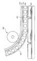
도 1은 일반적인 전자영동 표시장치의 개념도이다.1 is a conceptual diagram of a general electrophoretic display device.
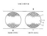
도 1을 참조하면, 일반적으로 전자영동 표시장치는 외부로부터 입사되는 광을 반사하여 영상을 표시하는 반사형 구조를 갖는다. 구체적으로, 전자영동 표시장치는 음의 전하로 대전된 백색의 잉크 입자(1)와 양의 전하로 대전된 검은색의 잉크 입자(2)와, 투명 유전유체(3)를 감싸는 마이크로캡슐(5)과 상기 마이크로캡슐(5)을 바인더와 혼합하여 양 전극 사이에 배치된 구조를 갖는다.Referring to FIG. 1, an electrophoretic display generally has a reflective structure that displays an image by reflecting light incident from the outside. Specifically, the electrophoretic display device includes a
상기 전자영동 표시장치는 상기 양 전극에 방향성 전계를 인가하여 시인 방향(VIEW DIRECTION)으로 백색 잉크 입자(1)가 모이면 백색이 표시되고, 반대로 검은색 잉크 입자(2)가 모이면 검은색이 표시되는 원리로 구동한다. 즉, 상기 시인 방향으로 움직인 상기 백색 잉크 입자들(1)에 의해 외부로부터 입사된 광이 반사되어 영상을 표시한다.The electrophoretic display applies a directional electric field to both electrodes to display white when the
상기 전자영동 표시장치는 외부로부터 입사된 광을 이용하여 영상을 표시하는 반사형 구조를 가짐에 따라 명암 대비비(Contrast Ratio : C/R)가 낮은 문제점 을 갖는다.The electrophoretic display has a low contrast ratio (C / R) as it has a reflective structure for displaying an image using light incident from the outside.
이에 본 발명의 기술적 과제는 이러한 종래의 문제점을 해결하기 위한 것으로, 본 발명의 목적은 백색 휘도 특성을 향상시키기 위한 컬러필터 기판을 제공하는 것이다.Accordingly, the technical problem of the present invention is to solve such a conventional problem, and an object of the present invention is to provide a color filter substrate for improving white luminance characteristics.
본 발명의 다른 목적은 상기 컬러필터 기판을 구비한 전자영동 표시장치를 제공하는 것이다.Another object of the present invention is to provide an electrophoretic display device having the color filter substrate.
상기한 본 발명의 목적을 실현하기 위한 실시예에 따른 컬러필터 기판은 공통 전극, 백색 차광부 및 컬러 필터층을 포함한다. 상기 백색 차광부는 상기 베이스 기판 위에 형성되고, 상기 베이스 기판을 투과 영역과 차광 영역으로 나눈다. 상기 컬러 필터층은 상기 투과 영역에 형성된다.The color filter substrate according to the embodiment for realizing the above object of the present invention includes a common electrode, a white light blocking portion, and a color filter layer. The white light blocking portion is formed on the base substrate, and divides the base substrate into a transmission region and a light blocking region. The color filter layer is formed in the transmission region.
상기한 본 발명의 다른 목적을 실현하기 위한 실시예에 따른 전자영동 표시장치는 어레이 기판, 컬러필터 기판 및 전자 영동층을 포함한다. 상기 어레이 기판은 제1 베이스 기판 위에 형성된 복수의 화소 전극들을 포함한다. 상기 컬러필터 기판은 제2 베이스 기판 위에 형성된 백색 차광부와, 상기 백색 차광부에 의해 정의된 투과 영역에 형성된 컬러 필터층을 포함한다. 상기 전자 영동층은 상기 어레이 기판과 상기 컬러필터 기판 사이에 개재되고, 양 전하 및 음 전하로 대전된 입자들을 포함한다.An electrophoretic display device according to an exemplary embodiment for realizing another object of the present invention includes an array substrate, a color filter substrate, and an electrophoretic layer. The array substrate includes a plurality of pixel electrodes formed on the first base substrate. The color filter substrate includes a white light blocking portion formed on the second base substrate, and a color filter layer formed in a transmission region defined by the white light blocking portion. The electrophoretic layer includes particles interposed between the array substrate and the color filter substrate and charged with positive and negative charges.
이러한 컬러필터 기판 및 이를 구비한 전자영동 표시장치에 의하면, 백색 차 광부를 형성함으로써 화소부들의 경계 구획 및 차광 기능은 물론 표시장치의 백색 휘도 특성을 향상시킬 수 있다.According to the color filter substrate and the electrophoretic display device including the same, the white light shielding part can improve the white luminance characteristics of the display device as well as the boundary partition and the light blocking function of the pixel parts.
도면에서 여러 층 및 영역을 명확하게 표현하기 위하여 두께를 확대하여 나타내었다. 상세한 설명에서 층, 막, 영역, 판 등의 부분이 다른 부분 "위에" 있다고 할 경우, 이는 다른 부분 "바로 위에" 있는 경우뿐만 아니라 그 중간에 또 다른 부분이 있는 경우도 포함한다. 반대로 층, 막, 영역, 판 등의 부분이 다른 부분 "아래에" 있다고 할 경우, 이는 다른 부분 "바로 아래에" 있는 경우뿐만 아니라 그 중간에 또 다른 부분이 있는 경우도 포함한다. 또한, 동일한 구성요소에 대해서는 동일한 도면부호를 부여하여 설명한다.In the drawings, the thickness is enlarged to clearly represent the layers and regions. In the description, when a layer, a film, an area, a plate, or the like is referred to as being "on" another part, it includes not only the case where it is "directly on" another part but also another part in between. On the contrary, where a section such as a layer, a film, an area, a plate, etc. is referred to as being "under" another section, this includes not only the case where the section is "directly underneath" In addition, the same components are described with the same reference numerals.
이하, 첨부한 도면들을 참조하여, 본 발명을 보다 상세하게 설명한다.DETAILED DESCRIPTION OF THE PREFERRED EMBODIMENTS The present invention will now be described in more detail with reference to the accompanying drawings.
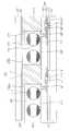
도 2는 본 발명의 실시예에 따른 전자영동 표시장치의 평면도이다. 도 3은 본 발명의 제1 실시예에 따른 전자영동 표시장치의 단면도로서, 도 2의 I-I'선으로 절단한 단면도이다.2 is a plan view of an electrophoretic display device according to an exemplary embodiment of the present invention. 3 is a cross-sectional view of the electrophoretic display device according to the first exemplary embodiment, taken along the line II ′ of FIG. 2.
도 2 및 도 3을 참조하면, 전자영동 표시장치는 어레이 기판(100), 전자 영동층(200) 및 컬러필터 기판(300)을 포함한다.2 and 3, the electrophoretic display includes an
상기 어레이 기판(100)은 제1 베이스 기판(101)을 포함한다. 상기 제1 베이스 기판(101)은 광을 차광 및 반사하는 재질로 형성되며, 바람직하게 거울이다. 상기 제1 베이스 기판(101) 위에는 제1 방향으로 연장된 게이트 배선들(GLn-1, GLn)과 상기 제1 방향과 교차하는 제2 방향으로 연장된 소스 배선들(DLm-1, DLm, DLm+1)이 형성된다. 상기 게이트 배선들(GLn-1, GLn)과 상기 소스 배선들(DLm-1, DLm, DLm+1)에 의해 상기 제1 베이스 기판(101)은 화소부들(P1, P2)이 정의된다.The
구체적으로, 제1 화소부(P1)는 해당하는 n번째 게이트 배선(GLn)과 m번째 소스 배선(DLm)에 연결된 제1 스위칭 소자(TFT1)와 상기 제1 스위칭 소자(TFT1)와 제1 콘택부(CT1)를 통해 전기적으로 연결된 제1 화소 전극(PE1)이 형성된다.In detail, the first pixel portion P1 includes a first switching element TFT1 connected to a corresponding nth gate line GLn and an mth source line DLm, and the first switching element TFT1 and a first contact. The first pixel electrode PE1 is electrically connected through the unit CT1.
상기 제1 스위칭 소자(TFT1)는 상기 n번째 게이트 배선(GL)과 연결된 제1 게이트 전극(GE1)과, 상기 제1 게이트 전극(GE1) 위에 형성된 게이트 절연층(120)과, 상기 게이트 절연층(120) 위에 형성된 제1 채널부(CH1)와, m번째 소스 배선(DLm)에 연결된 제1 소스 전극(SE1)과, 상기 제1 화소 전극(PE1)에 연결된 제1 드레인 전극(DE1)과, 상기 제1 소스 및 제1 드레인 전극(SE1, DE1) 위에 형성된 보호 절연층(140)을 포함한다. 상기 보호 절연층(140)은 도시된 바와 같이, 패시베이션층(120) 및 유기 절연층(130)을 포함하는 이중막 구조로 형성되거나, 패시베이션층(120)만으로 단일막 구조로 형성될 수 있다.The first switching element TFT1 may include a first gate electrode GE1 connected to the n-th gate line GL, a
상기 n번째 게이트 배선(GLn)에 게이트 신호가 인가되면 상기 제1 스위칭 소자(TFT1)는 턴-온 되고 상기 m번째 소스 배선(DLm)에 인가된 데이터 신호를 상기 제1 화소 전극(PE1)에 인가한다.When a gate signal is applied to the n-th gate line GLn, the first switching element TFT1 is turned on and a data signal applied to the m-th source line DLm is applied to the first pixel electrode PE1. Is authorized.
제2 화소부(P2)는 n번째 게이트 배선(GLn)과 m+1번째 소스 배선(DLm+1)에 연결된 제2 스위칭 소자(TFT2)와 상기 제2 스위칭 소자(TFT2)와 제2 콘택부(CT2)를 통해 전기적으로 연결된 제2 화소 전극(PE2)이 형성된다. 상기 제2 스위칭 소자(TFT2)는 도 2 및 도 3에 도시된 바와 같이, 상기 제1 스위칭 소자(TFT1)와 동일 한 구조로 형성되므로 상세한 설명은 생략한다.The second pixel portion P2 includes a second switching element TFT2 and the second switching element TFT2 and the second contact portion connected to the n-th gate line GLn and the m + 1th source line DLm + 1. The second pixel electrode PE2 is electrically connected through the CT2. Since the second switching device TFT2 is formed in the same structure as the first switching device TFT1 as shown in FIGS. 2 and 3, a detailed description thereof will be omitted.
상기 전자 영동층(200)은 복수의 마이크로캡슐들(210)과 상기 마이크로캡슐들(210)을 묶는 바인더(220)를 포함한다. 각 마이크로캡슐(210)은 양(+) 전하 및 음(-) 전하로 대전된 전자영도 입자들을 포함한다.The
구체적으로, 각 마이크로캡슐(210)은 음 전하(-) 또는 양 전하(+)로 대전된 백색 잉크 입자(211)와 상기 백색 잉크 입자(211)와 반대되는 전하로 대전된 검은색 잉크 입자(212) 및 투명 유전체(213)를 포함한다. 예컨대, 상기 백색 잉크 입자(211)는 양 전하(+)로 대전되고, 상기 검은색 잉크 입자(212)는 음 전하(-)로 대전된다. 외부로부터 입사된 외부 광(EXTERNAL LIGHT)이 상기 백색 잉크 입자(211)에 의해 직접 반사되어 백색을 표시한다.Specifically, each
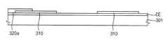
상기 컬러필터 기판(300)은 제2 베이스 기판(301)을 포함한다. 상기 제2 베이스 기판(301)은 유연성을 가지는 재질로 형성될 수 있다. 바람직하게 광 투과율, 내열성, 내화학성, 기계적 강도 등이 우수한 플라스틱 재질(PET)로 형성된다. 상기 제2 베이스 기판(301) 위에는 공통 전극(CE), 백색 차광부(WS) 및 컬러 필터층(320)이 형성된다.The
상기 공통 전극(CE)은 투명 도전성 물질로 형성되어, 상기 제1 및 제2 화소 전극들(PE1, PE2)과 대향하는 전극으로 공통 전압이 인가된다. 상기 투명한 전도성 물질, 예를 들어, 산화주석인듐(Indium Tin Oxide, ITO), 산화아연인듐(Indium Zinc Oxide, IZO), 아몰퍼스 산화주석인듐(amorphous Indium Tin Oxide, a-ITO) 등으로 이루어질 수 있다.The common electrode CE is formed of a transparent conductive material, and a common voltage is applied to an electrode facing the first and second pixel electrodes PE1 and PE2. The transparent conductive material, for example, may be made of indium tin oxide (ITO), indium zinc oxide (IZO), amorphous indium tin oxide (a-ITO), or the like. .
상기 백색 차광부(WS)는 상기 공통 전극(CE) 위에 직접 형성된다. 여기서 상기 공통 전극(CE)이 상기 제2 베이스 기판(301)과 접촉되도록 바로 위에 형성하는 것을 예로 하였으나, 상기 공통 전극(CE)은 상기 컬러 필터층(320) 위에 형성될 수 있다.The white light blocking part WS is directly formed on the common electrode CE. Herein, the common electrode CE is formed directly on the
상기 백색 차광부(WS)는 상기 제1 및 제2 화소 전극들(PE1, PE2)이 형성되지 않은 영역에 대응하여 형성되어, 상기 제2 베이스 기판(301)을 투과 영역과 차광 영역을 분리한다. 바람직하게 상기 백색 차광부(WS)는 제1 및 제2 스위칭 소자들(TFT1, TFT2)이 형성된 영역 및 게이트 및 소스 배선들(GLn, DLm-1, DLm, DLm+1)이 형성된 영역에 형성된다. 상기 백색 차광부(WS)는 산화티타늄 또는 산화알루미늄을 포함하는 재료이거나, 아크릴계 수지, 폴리스틸렌, 폴리에스터 등의 고분자 백색 물질로 형성될 수 있다.The white light blocking part WS is formed to correspond to an area where the first and second pixel electrodes PE1 and PE2 are not formed, and separates the
상기 백색 차광부(WS)가 상기 백색의 물질로 형성됨에 따라서, 외부 광(EXTERNAL LIGHT)을 차단함과 동시에 반사광을 이용하는 전자영동 표시장치의 명암 대비비(C/R)를 향상시킬 수 있다.As the white light blocking part WS is formed of the white material, the contrast ratio (C / R) of the electrophoretic display device using the reflected light may be improved while blocking the external light.
도 3에서는 상기 백색 차광부(WS)의 일 예로서, 막 패턴 형상을 갖는 백색 차광 패턴(310)이 개시되어 있다. 구체적으로, 상기 백색 차광 패턴(310)은 상기 화소부들간의 경계를 구분해 주고, 제1 및 제2 화소 전극들(PE1, PE2)이 형성되지 않은 부분과 제1 및 제2 화소 전극들(PE1, PE2)의 외곽부에 형성된 역 경사 도메인(Revers Tilted Domain)을 차폐시킨다. 또한, 스위칭 소자들(TFT1, TFT2)에 직접 광이 조사되는 것을 차단하여 상기 스위칭 소자들(TFT1, TFT2)의 누설 전류 증가를 방지한다. 또한 상기 어레이 기판(100)과의 결합 공정시 충분한 얼라인 마진을 확보한다.In FIG. 3, as an example of the white light blocking part WS, a white
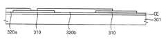
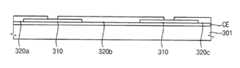
상기 컬러 필터층(320)은 상기 백색 차광 패턴(310)에 의해 정의된 투과 영역, 즉 화소 전극(PE1, PE2)이 형성된 영역에 대응하여 형성된다. 상기 컬러 필터층(320)은 적색, 녹색 및 청색 필터패턴들(320a, 320b)을 포함한다. 또한, 상기 컬러 필터층(320)은 백색 필터패턴(미도시)을 더 포함할 수도 있다. 상기 백색 필터패턴은 상기 적색, 녹색 및 청색 필터패턴을 중첩하여 형성하거나, 상기 제2 베이스 기판(301)을 노출시키는 방식으로 상기 컬러 필터층을 형성하지 않을 수도 있다.The
도시되지는 않았으나, 상기 컬러 필터층(320) 위에 형성되어 상기 적색, 녹색 및 청색 필터패턴들(320a, 320b)의 보호 및 평탄화를 위한 오버코팅층을 형성할 수 있다.Although not shown, an overcoat layer may be formed on the
상기 어레이 기판(100)의 상기 제1 및 제2 화소 전극들(PE1, PE2)과 상기 컬러필터 기판(300)의 공통 전극(CE) 사이에 개재된 상기 마이크로캡슐(210)은 상기 제1 및 제2 화소 전극들(PE1, PE2)과 공통 전극(CE) 사이에 형성되는 전계의 크기 및 방향에 따라 상기 백색 및 검은색 잉크 입자(211, 212)가 이동되어 계조를 표시한다.The
구체적으로, 상기 제1 화소 전극(PE1)에 공통 전극(CE)에 인가되는 공통전압(VCOM) 대비 음의 전압(-)을 인가하게 되면, 상기 양의 전하를 가진 백색 잉크 입자(211)가 상기 어레이 기판(100)측으로 이동하고 상대적으로 음의 전하를 가진 검은색 잉크 입자(212)가 상기 컬러필터 기판(300)측으로 이동하여 검은색 영상이 시인된다.In detail, when a negative voltage (−) is applied to the first pixel electrode PE1 compared to the common voltage VCOM applied to the common electrode CE, the
반대로, 상기 제1 화소 전극(PE1)에 상기 공통전압(VCOM) 대비 양의 전압(+)을 인가하게 되면, 상기 음의 전하를 가진 검은색 잉크 입자(212)가 상기 어레이 기판(100)측으로 이동하고 상대적으로 양의 전하를 가진 백색 잉크 입자(211)가 상기 컬러필터 기판(300)측으로 이동하여 백색 영상이 시인된다.On the contrary, when a positive voltage (+) is applied to the first pixel electrode PE1 compared to the common voltage VCOM, the
도 4a 내지 도 4e는 도 3의 컬러필터 기판의 제조 방법을 설명하기 위한 공정도들이다.4A through 4E are process diagrams for describing a method of manufacturing the color filter substrate of FIG. 3.
도 3 및 도 4a를 참조하면, 컬리필터 기판(300)은 제2 베이스 기판(301)을 포함한다. 상기 제2 베이스 기판(301)은 바람직하게 유연성을 갖는 투명한 플라스틱 필름으로 형성된다. 또한, 상기 제2 베이스 기판(301)은 광 투과율, 내열성, 내화학성, 기계적 강도 등이 우수한 플라스틱 재질로 형성될 수 있다.3 and 4A, the
상기 제2 베이스 기판(301) 위에 투명 도전성 물질로 공통 전극(CE)을 형성한다. 상기 투명한 전도성 물질, 예를 들어, 산화주석인듐(Indium Tin Oxide, ITO), 산화아연인듐(Indium Zinc Oxide, IZO), 아몰퍼스 산화주석인듐(amorphous Indium Tin Oxide, a-ITO) 등을 포함한다.The common electrode CE is formed of the transparent conductive material on the
상기 공통 전극(CE)이 형성된 제2 베이스 기판(301) 위에 백색의 무기 물질 또는 유기 물질(미도시)을 도포한다. 상기 백색 물질은 산화티타늄 또는 산화알루미늄을 포함하는 재료이거나, 아크릴계 수지, 폴리스틸렌, 폴리에스터 등의 고분자 백색 물질일 수 있다.A white inorganic material or an organic material (not shown) is coated on the
상기 백색의 물질을 패터닝하여 상기 제2 베이스 기판(301)을 투과 영역과 차광 영역을 정의하는 백색 차광 패턴(310)을 형성한다. 상기 백색 차광 패턴(310)은 상기 게이트 배선들(GLn-1, GLn), 소스 배선들(DLm-1, DLm, DLm+1) 및 스위칭 소자들(TFT1, TFT2)이 형성된 영역에 형성된다. 상기 백색 차광 패턴(310)은 백색으로 형성함에 따라서, 외부 광(EXTERNAL LIGHT)을 차단함과 동시에 반사광을 이용하는 전자영동 표시장치의 명암 대비비(C/R)를 향상시킬 수 있다.The white material is patterned to form a white
구체적으로, 상기 백색 차광 패턴(310)은 상기 화소부들(P1, P2)간의 경계를 구분해 주고, 상기 제1 및 제2 화소 전극들(PE1, PE2)이 형성되지 않은 부분과 상기 상기 제1 및 제2 화소 전극들(PE1, PE2)의 외곽부에 형성된 역 경사 도메인(Revers Tilted Domain)을 차폐시킨다. 또한, 상기 스위칭 소자들(TFT1, TFT2)에 직접 광이 조사되는 것을 차단하여 상기 스위칭 소자들(TFT1, TFT2)의 누설 전류 증가를 방지한다. 또한 상기 어레이 기판(100)과의 결합 공정시 충분한 얼라인 마진을 확보한다.In detail, the white
도 4b를 참조하면, 상기 백색 차광 패턴(310)이 형성된 제2 베이스 기판(301) 위에 적색 염료 또는 적색 안료가 포함된 제1 포토레지스트층(미도시)을 균일하게 도포한다. 이후, 상기 제1 포토레지스트층을 패터닝하여 적색 필터 패턴(320a)을 형성한다.Referring to FIG. 4B, a first photoresist layer (not shown) including a red dye or a red pigment is uniformly coated on the
도 4c를 참조하면, 상기 적색 필터 패턴(320a)이 형성된 제2 베이스 기판(301) 위에 녹색 염료 및 녹색 안료가 포함된 제2 포토레지스트층(미도시)을 균일하게 도포한다. 이후, 상기 제2 포토레지스트층을 패터닝하여 녹색 필터 패 턴(320b)을 형성한다.Referring to FIG. 4C, a second photoresist layer (not shown) including green dye and green pigment is uniformly coated on the
도 4d를 참조하면, 상기 적색 및 녹색 필터 패턴(320a, 320b)이 형성된 제2 베이스 기판(301) 위에 청색 염료 및 청색 안료가 포함된 제3 포토레지스트층(미도시)을 균일하게 도포한다. 이후, 상기 제3 포토레지스트층을 패터닝하여 청색 필터 패턴(320c)을 형성한다.Referring to FIG. 4D, a third photoresist layer (not shown) including a blue dye and a blue pigment is uniformly coated on the
도 4e를 참조하면, 상기 적색, 녹색 및 청색 필터 패턴(320a, 320b, 320c)이 형성된 제2 베이스 기판(301) 위에 복수의 마이크로캡슐들(210)을 분사 및 고정하여 전자 영동층(200)을 형성한다. 이후, 상기 전자 영동층(200) 위에 접착층(302)을 형성한다.Referring to FIG. 4E, the
도 5는 도 3에 도시된 전자영동 표시장치의 제조 방법을 설명하기 위한 공정도이다.FIG. 5 is a flowchart illustrating a method of manufacturing the electrophoretic display shown in FIG. 3.
도 3 및 도 5를 참조하면, 상기 전자 영동층(200)이 형성된 상기 컬러필터 기판(300)을 상기 어레이 기판(100)에 부착한다. 구체적으로, 라미네이터(400)를 이용하여 상기 전자 영동층(200)이 형성된 상기 컬러필터 기판(300)을 상기 제1 및 제2 화소 전극들(PE1, PE2)이 형성된 상기 어레이 기판(100)의 일면에 부착시킨다.3 and 5, the
상기 전자 영동층(200) 위에 형성된 접착층(302)에 의해 상기 컬러필터 기판(300)과 상기 어레이 기판(100)은 결합되고, 상기 컬러필터 기판(300)과 어레이 기판(100) 사이에는 상기 전자 영동층(200)이 개재된다.The
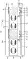
도 6은 본 발명의 제2 실시예에 따른 전자영동 표시장치의 단면도이다.6 is a cross-sectional view of an electrophoretic display device according to a second exemplary embodiment of the present invention.
도 6을 참조하면, 전자영동 표시장치는 어레이 기판(100), 전자 영동층(200) 및 컬러필터 기판(500)을 포함한다. 상기 어레이 기판(100) 및 전자 영동층(200)은 상기 도 3에서 설명된 바와 실질적 동일하므로 간략하게 설명한다.Referring to FIG. 6, an electrophoretic display includes an
상기 어레이 기판(100)은 서로 교차하는 방향으로 연장된 상기 게이트 배선들(GLn-1,GLn)과 소스 배선들(DLm-1, DLm, DLm+1)에 의해 정의된 화소부들에 복수의 화소 전극들(예컨대, 상기 제1 및 제2 화소 전극들(PE1, PE2)이 형성된다.The
상기 전자 영동층(200)은 복수의 마이크로캡슐들(210)과 상기 마이크로캡슐들(210)을 묶는 바인더(220)를 포함한다. 각 마이크로캡슐(210)은 음 전하(-) 또는 양 전하(+)로 대전된 백색 잉크 입자(211)와 상기 백색 잉크 입자(211)와 반대되는 전하로 대전된 검은색 잉크 입자(212) 및 투명 유전체(213)를 포함한다.The
상기 컬러필터 기판(500)은 제2 베이스 기판(501)을 포함한다. 상기 제2 베이스 기판(501)은 유연성을 가지는 재질로 형성될 수 있다. 바람직하게 광 투과율, 내열성, 내화학성, 기계적 강도 등이 우수한 플라스틱 재질(PET)로 형성된다.The
상기 제2 베이스 기판(501) 위에는 공통 전극(CE), 백색 격벽 패턴(510) 및 컬러 필터층(520)이 형성된다. 상기 백색 격벽 패턴(510)은 상기 백색 차광부(WS)의 일 예이다.The common electrode CE, the
상기 공통 전극(CE)은 투명 도전성 물질로 형성되어, 상기 제1 및 제2 화소 전극들(PE1, PE2)과 대향하는 전극으로 공통 전압이 인가된다. 여기서 상기 공통 전극(CE)이 상기 제2 베이스 기판(501)과 접촉되도록 바로 위에 형성하는 것을 예로 하였으나, 상기 공통 전극(CE)은 상기 컬러 필터층(520) 위에 형성될 수 있다.The common electrode CE is formed of a transparent conductive material, and a common voltage is applied to an electrode facing the first and second pixel electrodes PE1 and PE2. Although the common electrode CE is formed directly on the
상기 백색 격벽 패턴(510)은 상기 제1 및 제2 화소 전극들(PE1, PE2)이 형성 되지 않은 영역에 대응하여 형성되어 상기 제2 베이스 기판(501)을 투과 영역과 차광 영역을 분리하고, 각각의 화소 전극에 대응하여 화소 공간을 형성한다.The white
바람직하게 상기 백색 격벽 패턴(510)은 제1 및 제2 스위칭 소자(TFT1, TFT2)가 형성된 영역 및 상기 게이트 및 소스 배선들(GLn, DLm-1, DLm, DLm+1)이 형성된 영역에 형성되어, 상기 제1 및 제2 화소 전극들(PE1, PE2)에 대응하여 화소 공간들을 형성한다. 상기 백색 격벽 패턴(510)은 산화티타늄 또는 산화알루미늄을 포함하는 재료이거나, 아크릴계 수지, 폴리스틸렌, 폴리에스터 등의 고분자 백색 물질로 형성될 수 있다.Preferably, the white
상기 백색 격벽 패턴(510)에 의해 정의된 각 화소 공간에는 복수의 마이크로 캡슐(210)들이 채워진다. 상기 백색 격벽 패턴(510)의 단부는 상기 어레이 기판(100)과 직접 맞닿도록 결합되어 상기 마이크로 캡슐(210)들이 수용된 상기 화소 공간을 밀폐시킨다.A plurality of
결과적으로, 상기 제1 및 제2 화소 전극들(PE1, PE2)과 공통 전극(CE)에 인가되는 전압차에 의해 상기 마이크로 캡슐(210)들 내의 상기 잉크 입자들(211, 212)은 전계 방향에 대응하여 움직여 계조 영상을 표시한다.As a result, the
상기 백색 격벽 패턴(510)을 상기 백색 물질로 형성함에 따라서, 외부 광을 차단함과 동시에 반사광을 이용하는 전자영동 표시장치의 명암 대비비(C/R)를 향상시킬 수 있다.As the white
도 7은 본 발명의 제3 실시예에 따른 전자영동 표시장치의 단면도이다.7 is a cross-sectional view of an electrophoretic display device according to a third exemplary embodiment of the present invention.
도 7을 참조하면, 전자영동 표시장치는 어레이 기판(100), 전자 영동층(250) 및 컬러필터 기판(500)을 포함한다. 상기 어레이 기판(100)은 상기 도 3에서 설명된 바와 실질적 동일하고, 상기 컬러필터 기판(500)은 상기 도 6에서 설명된 바와 실질적으로 동일하므로 상기 어레이 기판(100) 및 컬러필터 기판(500)에 대해 간략하게 설명한다.Referring to FIG. 7, an electrophoretic display includes an
상기 어레이 기판(100)은 서로 교차하는 방향으로 연장된 상기 게이트 배선들과 소스 배선들에 의해 정의된 화소부들에 복수의 화소 전극들(예컨대, 상기 제1 및 제2 화소 전극들(PE1, PE2)이 형성된다.The
상기 컬러필터 기판(500)은 상기 제1 및 제2 화소 전극들(PE1, PE2)이 형성되지 않은 영역에 대응하여 화소 공간들을 정의하는 상기 백색 격벽 패턴(510)이 형성된다. 또한, 상기 컬러필터 기판(500)은 상기 화소 공간들에 대응하여 형성된 상기 컬러 필터층(520)을 포함하고, 상기 컬러 필터층(520)은 복수의 컬러필터패턴들(520a, 520b)을 포함한다.In the
상기 컬러필터 기판(500)은 상기 백색 격벽 패턴(510)에 의해 형성된 화소 공간들에 전자 영동층(250)을 형성한다.The
상기 전자 영동층(250)은 음 전하(-) 또는 양 전하(+)로 대전된 상기 백색 잉크 입자(251)와 상기 백색 잉크 입자(251)와 반대되는 전하로 대전된 검은색 잉크 입자(252)를 포함하며, 상기 화소 공간들에 채워진다.The
상기 백색 격벽 패턴(510)의 단부는 상기 어레이 기판(100)과 직접 맞닿도록 결합되어 상기 전자 영동층(250)이 수용된 상기 화소 공간들을 밀폐시킨다.An end portion of the
결과적으로, 상기 제1 및 제2 화소 전극들(PE1, PE2)과 공통 전극(CE)에 인 가되는 전압차에 의해 상기 백색 및 검은색 잉크 입자들(251, 252)은 전계 방향에 대응하여 움직여 계조 영상을 표시한다.As a result, the white and
도 8은 본 발명의 제4 실시예에 따른 전자영동 표시장치의 단면도이다.8 is a cross-sectional view of an electrophoretic display device according to a fourth exemplary embodiment of the present invention.
도 8을 참조하면, 전자영동 표시장치는 어레이 기판(100), 전자 영동층(200) 및 컬러필터 기판(600)을 포함한다. 상기 어레이 기판(100)은 상기 도 3에서 설명된 바와 실질적으로 동일하고, 상기 전자 영동층(200)은 상기 도 6에 설명된 바와 실질적으로 동일하므로 상세한 설명은 생략한다. 물론, 상기 전자 영동층(200)은 도 7에 설명된 바와 같이 구현할 수도 있다.Referring to FIG. 8, an electrophoretic display includes an
상기 컬러필터 기판(600)은 제2 베이스 기판(601)을 포함한다. 상기 제2 베이스 기판(601)은 유연성을 가지는 재질로 형성될 수 있다. 바람직하게 광 투과율, 내열성, 내화학성, 기계적 강도 등이 우수한 플라스틱 재질(PET)로 형성된다.The
상기 제2 베이스 기판(601) 위에는 백색 차광부(610), 컬러 필터층(620), 공통 전극(CE) 및 격벽 패턴(630)을 포함한다. 상기 백색 차광부(610)는 백색 물질로 형성된 백색 차광 패턴이다.The white light blocking part 610, the
구체적으로, 상기 제2 베이스 기판(601) 위에 상기 백색 차광 패턴(610)을 형성한다. 상기 백색 차광 패턴(610)은 상기 제1 및 제2 화소 전극들(PE1, PE2)이 형성되지 않은 영역에 대응하여 형성되어 상기 제2 베이스 기판(601)을 투과 영역과 차광 영역을 분리한다. 상기 백색 차광 패턴(610)은 산화티타늄 또는 산화알루미늄을 포함하는 재료이거나, 아크릴계 수지, 폴리스틸렌, 폴리에스터 등의 고분자 백색 물질로 형성될 수 있다.In detail, the white light blocking pattern 610 is formed on the
상기 백색 차광 패턴(610) 위에 상기 컬러 필터층(620)을 형성한다. 상기 컬러 필터층(620)은 상기 백색 차광 패턴(610)에 의해 정의된 투과 영역, 즉 제1 및 제2 화소 전극(PE1, PE2)이 형성된 영역에 대응하여 형성된다. 상기 컬러 필터층(620)은 적색, 녹색 및 청색 필터패턴들(620a, 620b)을 포함한다. 또한, 상기 컬러 필터층(620)은 백색 필터패턴(미도시)을 더 포함할 수도 있다. 상기 백색 필터패턴은 상기 적색, 녹색 및 청색 필터패턴을 중첩하여 형성하거나, 상기 제2 베이스 기판(601)을 노출시키는 방식으로 상기 컬러 필터층을 형성하지 않을 수도 있다.The
상기 컬러 필터층(620) 위에 공통 전극(CE)을 형성한다. 상기 공통 전극(CE)은 투명 도전성 물질로 형성되며, 상기 투명한 전도성 물질은 예를 들어, 산화주석인듐(Indium Tin Oxide, ITO), 산화아연인듐(Indium Zinc Oxide, IZO), 아몰퍼스 산화주석인듐(amorphous Indium Tin Oxide, a-ITO) 등으로 이루어질 수 있다.The common electrode CE is formed on the
상기 공통 전극(CE) 위에 상기 백색 차광 패턴(610)과 중첩되는 영역에 화소 공간을 형성하는 격벽 패턴(630)을 형성한다. 상기 격벽 패턴(630)은 백색 물질로 형성되거나, 검은색 물질로 형성될 수 있다. 바람직하게 상기 격벽 패턴(630)은 산화티타늄 또는 산화알루미늄을 포함하는 재료이거나, 아크릴계 수지, 폴리스틸렌, 폴리에스터 등의 고분자 백색 물질로 형성될 수 있다.A
상기 격벽 패턴(630)에 의해 형성된 화소 공간에는 복수의 마이크로 캡슐(210)들이 채워진다. 상기 격벽 패턴(630)의 단부는 상기 어레이 기판(100)과 직접 맞닿도록 결합되어 상기 마이크로 캡슐(210)들이 수용된 상기 화소 공간을 밀폐 시킨다.The
결과적으로, 상기 제1 및 제2 화소 전극들(PE1, PE2)과 공통 전극(CE)에 인가되는 전압차에 의해 상기 마이크로 캡슐(210)들 내의 상기 잉크 입자들(211, 212)은 전계 방향에 대응하여 움직여 계조 영상을 표시한다.As a result, the
상기 제4 실시예에 따른 전자영동 표시장치는 상기 백색 차광부(610)에 의해 외부 광을 차단함과 동시에 반사광을 이용하는 전자영동 표시장치의 명암 대비비(C/R)를 향상시킬 수 있다.The electrophoretic display device according to the fourth exemplary embodiment may block the external light by the white light blocking part 610 and improve the contrast ratio (C / R) of the electrophoretic display device using the reflected light.
이상에서 설명한 바와 같이, 본 발명에 따르면 외부 광을 반사하여 영상을 표시하는 전자영동 표시장치에서 화소부들을 경계짓는 차광부를 백색 물질로 형성함으로써 차광 기능은 물론 명암 대비비를 향상시킬 수 있다. 이에 따라서, 상대적으로 백색 휘도 특성 및 명암 대비비가 낮은 전자영동 표시장치의 근본적인 문제를 해결할 수 있다.As described above, according to the present invention, in the electrophoretic display device that displays an image by reflecting external light, the light blocking part that borders the pixel parts is formed of a white material, thereby improving light blocking function and contrast ratio. Accordingly, it is possible to solve the fundamental problem of the electrophoretic display device having relatively low white luminance characteristics and low contrast ratio.
이상에서는 실시예를 참조하여 설명하였지만, 해당 기술 분야의 숙련된 당업자는 하기의 특허 청구의 범위에 기재된 본 발명의 사상 및 영역으로부터 벗어나지 않는 범위 내에서 본 발명을 다양하게 수정 및 변경시킬 수 있음을 이해할 수 있을 것이다.Although described above with reference to the embodiments, those skilled in the art can be variously modified and changed within the scope of the invention without departing from the spirit and scope of the invention described in the claims below. I can understand.
Claims (22)
Translated fromKoreanPriority Applications (7)
| Application Number | Priority Date | Filing Date | Title |
|---|---|---|---|
| KR1020060114294AKR101316636B1 (en) | 2006-11-20 | 2006-11-20 | Color filter substrate and electro-phoretic display device having the same |
| US11/933,353US7656577B2 (en) | 2006-11-20 | 2007-10-31 | Color filter substrate, electrophoretic display device having the same, and method of manufacturing the same |
| US11/931,179US7626753B2 (en) | 2006-11-20 | 2007-10-31 | Color filter substrate, electrophoretic display device having the same, and method thereof |
| PL07021895TPL1923733T3 (en) | 2006-11-20 | 2007-11-12 | Color filter substrate and electrophoretic display device having the same |
| DE602007006131TDE602007006131D1 (en) | 2006-11-20 | 2007-11-12 | Color filter substrate and electrophoretic display device with such a substrate |
| EP07021895AEP1923733B1 (en) | 2006-11-20 | 2007-11-12 | Color filter substrate and electrophoretic display device having the same |
| JP2007299184AJP5519904B2 (en) | 2006-11-20 | 2007-11-19 | Color filter substrate, electrophoretic display device including the same, and method for improving white light characteristics thereof |
Applications Claiming Priority (1)
| Application Number | Priority Date | Filing Date | Title |
|---|---|---|---|
| KR1020060114294AKR101316636B1 (en) | 2006-11-20 | 2006-11-20 | Color filter substrate and electro-phoretic display device having the same |
Publications (2)
| Publication Number | Publication Date |
|---|---|
| KR20080045333A KR20080045333A (en) | 2008-05-23 |
| KR101316636B1true KR101316636B1 (en) | 2013-10-15 |
Family
ID=39047630
Family Applications (1)
| Application Number | Title | Priority Date | Filing Date |
|---|---|---|---|
| KR1020060114294AExpired - Fee RelatedKR101316636B1 (en) | 2006-11-20 | 2006-11-20 | Color filter substrate and electro-phoretic display device having the same |
Country Status (6)
| Country | Link |
|---|---|
| US (1) | US7626753B2 (en) |
| EP (1) | EP1923733B1 (en) |
| JP (1) | JP5519904B2 (en) |
| KR (1) | KR101316636B1 (en) |
| DE (1) | DE602007006131D1 (en) |
| PL (1) | PL1923733T3 (en) |
Families Citing this family (23)
| Publication number | Priority date | Publication date | Assignee | Title |
|---|---|---|---|---|
| JP5270547B2 (en)* | 2006-08-08 | 2013-08-21 | コーニンクレッカ フィリップス エレクトロニクス エヌ ヴィ | Improved moving particle display |
| US7656577B2 (en)* | 2006-11-20 | 2010-02-02 | Samsung Electronics Co., Ltd. | Color filter substrate, electrophoretic display device having the same, and method of manufacturing the same |
| TWI387785B (en)* | 2009-01-09 | 2013-03-01 | Prime View Int Co Ltd | Method for manufacturing display panel and method for manufacturing the same |
| KR101276749B1 (en) | 2009-08-03 | 2013-06-19 | 엘지디스플레이 주식회사 | Electrophoretic display device and manufacturing method thereof |
| CN102221777A (en)* | 2010-04-16 | 2011-10-19 | 奇美实业股份有限公司 | White photosensitive resin composition and white matrix, color filter and reflective display assembly thereof |
| KR20120057682A (en) | 2010-08-06 | 2012-06-07 | 삼성모바일디스플레이주식회사 | Electro phoretic indication display and driving method thereof |
| KR101766878B1 (en)* | 2011-02-28 | 2017-08-10 | 삼성디스플레이 주식회사 | Electro phoretic display and method for manufacturing the same |
| CN102681282A (en)* | 2011-03-17 | 2012-09-19 | 凸版印刷株式会社 | Multi-color display board and manufacturing method thereof |
| CN102645691B (en)* | 2011-07-12 | 2014-07-23 | 京东方科技集团股份有限公司 | Color filter and manufacturing method thereof |
| TWI489212B (en) | 2013-03-29 | 2015-06-21 | Chi Mei Corp | Photosensitive resin composition and its application |
| JP2016177077A (en)* | 2015-03-19 | 2016-10-06 | 大日本印刷株式会社 | Color filter and display device |
| CN106383424A (en)* | 2015-07-31 | 2017-02-08 | 元太科技工业股份有限公司 | Reflective display device |
| US9529189B1 (en)* | 2015-09-30 | 2016-12-27 | Amazon Technologies, Inc. | Reflectance in electrowetting displays |
| KR102449405B1 (en)* | 2015-12-04 | 2022-09-29 | 엘지디스플레이 주식회사 | Transparent display device, and method for fabricating the same |
| CN106328016B (en)* | 2016-09-29 | 2017-12-15 | 京东方科技集团股份有限公司 | Display panel and its manufacture method, display device |
| CN107092127B (en)* | 2017-07-06 | 2022-03-04 | 京东方科技集团股份有限公司 | Refractive index adjustment structure, color filter substrate, display panel and display device |
| KR102054553B1 (en)* | 2017-09-25 | 2019-12-10 | 주식회사 엘지화학 | Transparent electrode substrate and method for manufacturing thereof |
| CN108761898A (en)* | 2018-03-30 | 2018-11-06 | 重庆京东方显示照明有限公司 | A kind of reflector plate and its control method, backlight module, display device |
| CN112505938B (en)* | 2019-08-26 | 2022-07-05 | 昇印光电(昆山)股份有限公司 | Stereo imaging film |
| CN115113452A (en)* | 2021-03-22 | 2022-09-27 | 川奇光电科技(扬州)有限公司 | Preparation method of display panel |
| CN113138516B (en)* | 2021-04-20 | 2022-10-04 | 深圳市弘德胜自动化设备有限公司 | Electronic paper filling and sealing equipment |
| CN113985676A (en)* | 2021-11-04 | 2022-01-28 | Tcl华星光电技术有限公司 | Electrophoresis display panel, manufacturing method and electronic device |
| CN114167640B (en)* | 2021-11-24 | 2023-05-30 | 武汉华星光电技术有限公司 | Manufacturing method of color film substrate |
Citations (2)
| Publication number | Priority date | Publication date | Assignee | Title |
|---|---|---|---|---|
| JP2002023351A (en)* | 2000-07-05 | 2002-01-23 | Toray Ind Inc | Photosensitive paste and member for display |
| US20040145562A1 (en)* | 2002-10-28 | 2004-07-29 | Tomonari Horikiri | Electrophoretic display and process for producing the same |
Family Cites Families (14)
| Publication number | Priority date | Publication date | Assignee | Title |
|---|---|---|---|---|
| FR2721427B1 (en) | 1994-06-17 | 1996-08-14 | Bruno Vinouze | Diffusing grid liquid crystal display screen. |
| JP3576657B2 (en)* | 1994-10-18 | 2004-10-13 | 株式会社東芝 | Reflective liquid crystal display |
| JP3556364B2 (en) | 1995-12-27 | 2004-08-18 | 富士通ディスプレイテクノロジーズ株式会社 | Active matrix type liquid crystal display panel and projection type display device |
| US5920364A (en) | 1998-08-07 | 1999-07-06 | Motorola, Inc. | Liquid crystal display device with masked images |
| US6829078B2 (en)* | 2000-03-03 | 2004-12-07 | Sipix Imaging Inc. | Electrophoretic display and novel process for its manufacture |
| JP4059034B2 (en)* | 2001-08-20 | 2008-03-12 | セイコーエプソン株式会社 | Electrophoresis device, electronic apparatus, and method of manufacturing the electrophoresis device |
| JP4168649B2 (en)* | 2002-04-05 | 2008-10-22 | コニカミノルタホールディングス株式会社 | Image recording device |
| JP2003330047A (en)* | 2002-05-10 | 2003-11-19 | Seiko Epson Corp | Electro-optical device, method of manufacturing the same, and electronic apparatus |
| JP2004020758A (en)* | 2002-06-14 | 2004-01-22 | Canon Inc | Display device |
| JP2004317526A (en)* | 2003-02-27 | 2004-11-11 | Bridgestone Corp | Panel for picture display, and picture display device |
| JP2004361514A (en)* | 2003-06-02 | 2004-12-24 | Canon Inc | Electrophoretic display |
| JP2005122101A (en)* | 2003-09-25 | 2005-05-12 | Seiko Epson Corp | Electro-optic device |
| JP2005321769A (en)* | 2004-04-07 | 2005-11-17 | Bridgestone Corp | Information display panel |
| JP4353153B2 (en)* | 2004-11-18 | 2009-10-28 | セイコーエプソン株式会社 | Display device, manufacturing method thereof, and electronic device |
- 2006
- 2006-11-20KRKR1020060114294Apatent/KR101316636B1/ennot_activeExpired - Fee Related
- 2007
- 2007-10-31USUS11/931,179patent/US7626753B2/ennot_activeExpired - Fee Related
- 2007-11-12DEDE602007006131Tpatent/DE602007006131D1/enactiveActive
- 2007-11-12EPEP07021895Apatent/EP1923733B1/ennot_activeNot-in-force
- 2007-11-12PLPL07021895Tpatent/PL1923733T3/enunknown
- 2007-11-19JPJP2007299184Apatent/JP5519904B2/ennot_activeExpired - Fee Related
Patent Citations (2)
| Publication number | Priority date | Publication date | Assignee | Title |
|---|---|---|---|---|
| JP2002023351A (en)* | 2000-07-05 | 2002-01-23 | Toray Ind Inc | Photosensitive paste and member for display |
| US20040145562A1 (en)* | 2002-10-28 | 2004-07-29 | Tomonari Horikiri | Electrophoretic display and process for producing the same |
Also Published As
| Publication number | Publication date |
|---|---|
| EP1923733B1 (en) | 2010-04-28 |
| US7626753B2 (en) | 2009-12-01 |
| JP5519904B2 (en) | 2014-06-11 |
| US20080117496A1 (en) | 2008-05-22 |
| EP1923733A1 (en) | 2008-05-21 |
| JP2008129599A (en) | 2008-06-05 |
| DE602007006131D1 (en) | 2010-06-10 |
| KR20080045333A (en) | 2008-05-23 |
| PL1923733T3 (en) | 2010-10-29 |
Similar Documents
| Publication | Publication Date | Title |
|---|---|---|
| KR101316636B1 (en) | Color filter substrate and electro-phoretic display device having the same | |
| US10564479B2 (en) | Display device | |
| US7656577B2 (en) | Color filter substrate, electrophoretic display device having the same, and method of manufacturing the same | |
| TWI418911B (en) | Electro-phoretic display and fabricating method thereof | |
| US7277219B2 (en) | Particle movement-type display device and particle movement-type display apparatus | |
| KR20080061039A (en) | Electrophoretic display device and manufacturing method thereof | |
| KR100553055B1 (en) | Electrophoretic display | |
| CN110346988A (en) | Display device | |
| KR20110042674A (en) | Display Array Board | |
| TWI680328B (en) | Display apparatus and manufacturing method thereof | |
| CN101246275A (en) | Display panel and display device with the display panel | |
| JP2004170903A (en) | Electrophoretic display | |
| US7408697B2 (en) | Display device and method for manufacturing the same, and electronic apparatus | |
| US20130114126A1 (en) | Multi-color electrophoretic display device, image sheet, and manufacturing method thereof | |
| JP2008020772A (en) | Liquid crystal display panel | |
| CN217718925U (en) | Display device | |
| KR101534626B1 (en) | Electrophoretic display device and method of forming the partition wall | |
| KR101908460B1 (en) | Display substrate, method of manufacturing the same and display apparatus having the same | |
| JP2005148740A (en) | Reflection type liquid crystal display of dual display | |
| JP2007140533A (en) | Electrophoretic display device and driving method of electrophoretic display device | |
| KR102555404B1 (en) | Flexible Display and Method for Manufacturing the Same | |
| US20130003164A1 (en) | Electrophoretic display device and driving method thereof | |
| CN108897180B (en) | Display panel, display device and display method thereof | |
| JP2006091546A (en) | Particle movement type display device | |
| KR101662135B1 (en) | Electrophoretic display panel, method of manufacturing the same and electrophoretic display apparatus having the same |
Legal Events
| Date | Code | Title | Description |
|---|---|---|---|
| PA0109 | Patent application | St.27 status event code:A-0-1-A10-A12-nap-PA0109 | |
| PG1501 | Laying open of application | St.27 status event code:A-1-1-Q10-Q12-nap-PG1501 | |
| A201 | Request for examination | ||
| PA0201 | Request for examination | St.27 status event code:A-1-2-D10-D11-exm-PA0201 | |
| R18-X000 | Changes to party contact information recorded | St.27 status event code:A-3-3-R10-R18-oth-X000 | |
| N231 | Notification of change of applicant | ||
| PN2301 | Change of applicant | St.27 status event code:A-3-3-R10-R13-asn-PN2301 St.27 status event code:A-3-3-R10-R11-asn-PN2301 | |
| PE0902 | Notice of grounds for rejection | St.27 status event code:A-1-2-D10-D21-exm-PE0902 | |
| E13-X000 | Pre-grant limitation requested | St.27 status event code:A-2-3-E10-E13-lim-X000 | |
| P11-X000 | Amendment of application requested | St.27 status event code:A-2-2-P10-P11-nap-X000 | |
| P13-X000 | Application amended | St.27 status event code:A-2-2-P10-P13-nap-X000 | |
| E701 | Decision to grant or registration of patent right | ||
| PE0701 | Decision of registration | St.27 status event code:A-1-2-D10-D22-exm-PE0701 | |
| GRNT | Written decision to grant | ||
| PR0701 | Registration of establishment | St.27 status event code:A-2-4-F10-F11-exm-PR0701 | |
| PR1002 | Payment of registration fee | St.27 status event code:A-2-2-U10-U11-oth-PR1002 Fee payment year number:1 | |
| PG1601 | Publication of registration | St.27 status event code:A-4-4-Q10-Q13-nap-PG1601 | |
| R18-X000 | Changes to party contact information recorded | St.27 status event code:A-5-5-R10-R18-oth-X000 | |
| L13-X000 | Limitation or reissue of ip right requested | St.27 status event code:A-2-3-L10-L13-lim-X000 | |
| U15-X000 | Partial renewal or maintenance fee paid modifying the ip right scope | St.27 status event code:A-4-4-U10-U15-oth-X000 | |
| PR1001 | Payment of annual fee | St.27 status event code:A-4-4-U10-U11-oth-PR1001 Fee payment year number:4 | |
| LAPS | Lapse due to unpaid annual fee | ||
| PC1903 | Unpaid annual fee | St.27 status event code:A-4-4-U10-U13-oth-PC1903 Not in force date:20171003 Payment event data comment text:Termination Category : DEFAULT_OF_REGISTRATION_FEE | |
| PC1903 | Unpaid annual fee | St.27 status event code:N-4-6-H10-H13-oth-PC1903 Ip right cessation event data comment text:Termination Category : DEFAULT_OF_REGISTRATION_FEE Not in force date:20171003 | |
| R18-X000 | Changes to party contact information recorded | St.27 status event code:A-5-5-R10-R18-oth-X000 | |
| P22-X000 | Classification modified | St.27 status event code:A-4-4-P10-P22-nap-X000 |