KR101314383B1 - New compounds and organic electronic device using the same - Google Patents
New compounds and organic electronic device using the sameDownload PDFInfo
- Publication number
- KR101314383B1 KR101314383B1KR1020090064540AKR20090064540AKR101314383B1KR 101314383 B1KR101314383 B1KR 101314383B1KR 1020090064540 AKR1020090064540 AKR 1020090064540AKR 20090064540 AKR20090064540 AKR 20090064540AKR 101314383 B1KR101314383 B1KR 101314383B1
- Authority
- KR
- South Korea
- Prior art keywords
- group
- substituted
- unsubstituted
- compound
- organic
- Prior art date
- Legal status (The legal status is an assumption and is not a legal conclusion. Google has not performed a legal analysis and makes no representation as to the accuracy of the status listed.)
- Active
Links
- 150000001875compoundsChemical class0.000titleclaimsabstractdescription164
- 238000002347injectionMethods0.000claimsabstractdescription30
- 239000007924injectionSubstances0.000claimsabstractdescription30
- 230000005525hole transportEffects0.000claimsabstractdescription14
- 239000011368organic materialSubstances0.000claimsdescription36
- 125000003118aryl groupChemical group0.000claimsdescription26
- 238000000034methodMethods0.000claimsdescription21
- 238000004519manufacturing processMethods0.000claimsdescription16
- -1phosphoryl groupsChemical group0.000claimsdescription15
- KDLHZDBZIXYQEI-UHFFFAOYSA-NPalladiumChemical compound[Pd]KDLHZDBZIXYQEI-UHFFFAOYSA-N0.000claimsdescription14
- 125000003277amino groupChemical group0.000claimsdescription11
- 125000005264aryl amine groupChemical group0.000claimsdescription11
- 125000000217alkyl groupChemical group0.000claimsdescription10
- 125000000392cycloalkenyl groupChemical group0.000claimsdescription10
- 125000000753cycloalkyl groupChemical group0.000claimsdescription10
- 125000001072heteroaryl groupChemical group0.000claimsdescription10
- 125000003342alkenyl groupChemical group0.000claimsdescription9
- 125000003282alkyl amino groupChemical group0.000claimsdescription8
- 229910052760oxygenInorganic materials0.000claimsdescription7
- 125000003545alkoxy groupChemical group0.000claimsdescription6
- 125000005843halogen groupChemical group0.000claimsdescription6
- 125000004435hydrogen atomChemical group[H]*0.000claimsdescription6
- 229910052757nitrogenInorganic materials0.000claimsdescription6
- 229910052763palladiumInorganic materials0.000claimsdescription6
- ZOXJGFHDIHLPTG-UHFFFAOYSA-NBoronChemical group[B]ZOXJGFHDIHLPTG-UHFFFAOYSA-N0.000claimsdescription5
- BLRPTPMANUNPDV-UHFFFAOYSA-NSilaneChemical group[SiH4]BLRPTPMANUNPDV-UHFFFAOYSA-N0.000claimsdescription5
- 125000005377alkyl thioxy groupChemical group0.000claimsdescription5
- 125000005165aryl thioxy groupChemical group0.000claimsdescription5
- 229910052805deuteriumInorganic materials0.000claimsdescription5
- 125000004185ester groupChemical group0.000claimsdescription5
- 125000005842heteroatomChemical group0.000claimsdescription5
- 125000002887hydroxy groupChemical group[H]O*0.000claimsdescription5
- 125000000449nitro groupChemical group[O-][N+](*)=O0.000claimsdescription5
- 229910052739hydrogenInorganic materials0.000claimsdescription4
- 239000001257hydrogenSubstances0.000claimsdescription4
- YZCKVEUIGOORGS-OUBTZVSYSA-NDeuteriumChemical compound[2H]YZCKVEUIGOORGS-OUBTZVSYSA-N0.000claimsdescription3
- 150000003974aralkylaminesChemical group0.000claimsdescription3
- 125000002915carbonyl groupChemical group[*:2]C([*:1])=O0.000claimsdescription3
- 125000004093cyano groupChemical group*C#N0.000claimsdescription3
- 125000005462imide groupChemical group0.000claimsdescription3
- 229910052717sulfurInorganic materials0.000claimsdescription3
- 125000000923(C1-C30) alkyl groupChemical group0.000claimsdescription2
- 125000000739C2-C30 alkenyl groupChemical group0.000claimsdescription2
- UFHFLCQGNIYNRP-UHFFFAOYSA-NHydrogenChemical compound[H][H]UFHFLCQGNIYNRP-UHFFFAOYSA-N0.000claimsdescription2
- 125000001931aliphatic groupChemical group0.000claimsdescription2
- 125000003368amide groupChemical group0.000claimsdescription2
- 125000004104aryloxy groupChemical group0.000claimsdescription2
- 125000004429atomChemical group0.000claimsdescription2
- 125000005708carbonyloxy groupChemical group[*:2]OC([*:1])=O0.000claimsdescription2
- 239000003054catalystSubstances0.000claimsdescription2
- 125000000592heterocycloalkyl groupChemical group0.000claimsdescription2
- 125000002560nitrile groupChemical group0.000claimsdescription2
- GBXQPDCOMJJCMJ-UHFFFAOYSA-Mtrimethyl-[6-(trimethylazaniumyl)hexyl]azanium;bromideChemical compound[Br-].C[N+](C)(C)CCCCCC[N+](C)(C)CGBXQPDCOMJJCMJ-UHFFFAOYSA-M0.000claimsdescription2
- 150000003973alkyl aminesChemical class0.000claims1
- 150000001543aryl boronic acidsChemical class0.000claims1
- 230000008878couplingEffects0.000claims1
- 238000010168coupling processMethods0.000claims1
- 238000005859coupling reactionMethods0.000claims1
- 150000001975deuteriumChemical group0.000claims1
- 239000000463materialSubstances0.000abstractdescription60
- 239000010410layerSubstances0.000description110
- 238000002360preparation methodMethods0.000description44
- 238000006243chemical reactionMethods0.000description16
- 239000000758substrateSubstances0.000description16
- 230000032258transportEffects0.000description14
- XLYOFNOQVPJJNP-UHFFFAOYSA-NwaterChemical compoundOXLYOFNOQVPJJNP-UHFFFAOYSA-N0.000description14
- 239000012153distilled waterSubstances0.000description13
- 239000002019doping agentSubstances0.000description11
- 239000012044organic layerSubstances0.000description11
- 239000000126substanceSubstances0.000description11
- RFFLAFLAYFXFSW-UHFFFAOYSA-N1,2-dichlorobenzeneChemical compoundClC1=CC=CC=C1ClRFFLAFLAYFXFSW-UHFFFAOYSA-N0.000description10
- LFQSCWFLJHTTHZ-UHFFFAOYSA-NEthanolChemical compoundCCOLFQSCWFLJHTTHZ-UHFFFAOYSA-N0.000description10
- WYURNTSHIVDZCO-UHFFFAOYSA-NTetrahydrofuranChemical compoundC1CCOC1WYURNTSHIVDZCO-UHFFFAOYSA-N0.000description10
- 230000015572biosynthetic processEffects0.000description10
- 239000000243solutionSubstances0.000description10
- 125000001424substituent groupChemical group0.000description10
- 238000003786synthesis reactionMethods0.000description10
- YMWUJEATGCHHMB-UHFFFAOYSA-NDichloromethaneChemical compoundClCClYMWUJEATGCHHMB-UHFFFAOYSA-N0.000description9
- UKTSSJJZFVGTCG-UHFFFAOYSA-N(4-bromophenyl)-trimethylsilaneChemical compoundC[Si](C)(C)C1=CC=C(Br)C=C1UKTSSJJZFVGTCG-UHFFFAOYSA-N0.000description8
- QARVLSVVCXYDNA-UHFFFAOYSA-NbromobenzeneChemical compoundBrC1=CC=CC=C1QARVLSVVCXYDNA-UHFFFAOYSA-N0.000description8
- 125000004432carbon atomChemical groupC*0.000description8
- PQXKHYXIUOZZFA-UHFFFAOYSA-Mlithium fluorideChemical compound[Li+].[F-]PQXKHYXIUOZZFA-UHFFFAOYSA-M0.000description8
- 239000007787solidSubstances0.000description7
- CSCPPACGZOOCGX-UHFFFAOYSA-NAcetoneChemical compoundCC(C)=OCSCPPACGZOOCGX-UHFFFAOYSA-N0.000description6
- KFZMGEQAYNKOFK-UHFFFAOYSA-NIsopropanolChemical compoundCC(C)OKFZMGEQAYNKOFK-UHFFFAOYSA-N0.000description6
- OKKJLVBELUTLKV-UHFFFAOYSA-NMethanolChemical compoundOCOKKJLVBELUTLKV-UHFFFAOYSA-N0.000description6
- YXFVVABEGXRONW-UHFFFAOYSA-NTolueneChemical compoundCC1=CC=CC=C1YXFVVABEGXRONW-UHFFFAOYSA-N0.000description6
- 229910052751metalInorganic materials0.000description6
- 239000002184metalSubstances0.000description6
- 239000002904solventSubstances0.000description6
- 238000003756stirringMethods0.000description6
- VZSRBBMJRBPUNF-UHFFFAOYSA-N2-(2,3-dihydro-1H-inden-2-ylamino)-N-[3-oxo-3-(2,4,6,7-tetrahydrotriazolo[4,5-c]pyridin-5-yl)propyl]pyrimidine-5-carboxamideChemical compoundC1C(CC2=CC=CC=C12)NC1=NC=C(C=N1)C(=O)NCCC(N1CC2=C(CC1)NN=N2)=OVZSRBBMJRBPUNF-UHFFFAOYSA-N0.000description5
- 229910052782aluminiumInorganic materials0.000description5
- XAGFODPZIPBFFR-UHFFFAOYSA-NaluminiumChemical compound[Al]XAGFODPZIPBFFR-UHFFFAOYSA-N0.000description5
- 238000000151depositionMethods0.000description5
- 238000004770highest occupied molecular orbitalMethods0.000description5
- HEDRZPFGACZZDS-UHFFFAOYSA-NChloroformChemical compoundClC(Cl)ClHEDRZPFGACZZDS-UHFFFAOYSA-N0.000description4
- YLQBMQCUIZJEEH-UHFFFAOYSA-NFuranChemical groupC=1C=COC=1YLQBMQCUIZJEEH-UHFFFAOYSA-N0.000description4
- CSNNHWWHGAXBCP-UHFFFAOYSA-LMagnesium sulfateChemical compound[Mg+2].[O-][S+2]([O-])([O-])[O-]CSNNHWWHGAXBCP-UHFFFAOYSA-L0.000description4
- PCLIMKBDDGJMGD-UHFFFAOYSA-NN-bromosuccinimideChemical compoundBrN1C(=O)CCC1=OPCLIMKBDDGJMGD-UHFFFAOYSA-N0.000description4
- XLOMVQKBTHCTTD-UHFFFAOYSA-NZinc monoxideChemical compound[Zn]=OXLOMVQKBTHCTTD-UHFFFAOYSA-N0.000description4
- IJOOHPMOJXWVHK-UHFFFAOYSA-NchlorotrimethylsilaneChemical compoundC[Si](C)(C)ClIJOOHPMOJXWVHK-UHFFFAOYSA-N0.000description4
- 230000008021depositionEffects0.000description4
- 239000003599detergentSubstances0.000description4
- 239000011541reaction mixtureSubstances0.000description4
- 238000005406washingMethods0.000description4
- DMEVMYSQZPJFOK-UHFFFAOYSA-N3,4,5,6,9,10-hexazatetracyclo[12.4.0.02,7.08,13]octadeca-1(18),2(7),3,5,8(13),9,11,14,16-nonaeneChemical groupN1=NN=C2C3=CC=CC=C3C3=CC=NN=C3C2=N1DMEVMYSQZPJFOK-UHFFFAOYSA-N0.000description3
- 150000004982aromatic aminesChemical class0.000description3
- 239000010406cathode materialSubstances0.000description3
- 239000000460chlorineSubstances0.000description3
- 238000000576coating methodMethods0.000description3
- 229920001940conductive polymerPolymers0.000description3
- 230000021615conjugationEffects0.000description3
- 238000010438heat treatmentMethods0.000description3
- AMGQUBHHOARCQH-UHFFFAOYSA-Nindium;oxotinChemical compound[In].[Sn]=OAMGQUBHHOARCQH-UHFFFAOYSA-N0.000description3
- 229910044991metal oxideInorganic materials0.000description3
- 150000004706metal oxidesChemical class0.000description3
- VLKZOEOYAKHREP-UHFFFAOYSA-Nn-HexaneChemical compoundCCCCCCVLKZOEOYAKHREP-UHFFFAOYSA-N0.000description3
- 239000012299nitrogen atmosphereSubstances0.000description3
- 230000008569processEffects0.000description3
- 239000004065semiconductorSubstances0.000description3
- AITNMTXHTIIIBB-UHFFFAOYSA-N1-bromo-4-fluorobenzeneChemical compoundFC1=CC=C(Br)C=C1AITNMTXHTIIIBB-UHFFFAOYSA-N0.000description2
- UJOBWOGCFQCDNV-UHFFFAOYSA-N9H-carbazoleChemical compoundC1=CC=C2C3=CC=CC=C3NC2=C1UJOBWOGCFQCDNV-UHFFFAOYSA-N0.000description2
- NLXLAEXVIDQMFP-UHFFFAOYSA-NAmmonia chlorideChemical compound[NH4+].[Cl-]NLXLAEXVIDQMFP-UHFFFAOYSA-N0.000description2
- IJGRMHOSHXDMSA-UHFFFAOYSA-NAtomic nitrogenChemical compoundN#NIJGRMHOSHXDMSA-UHFFFAOYSA-N0.000description2
- RTZKZFJDLAIYFH-UHFFFAOYSA-NDiethyl etherChemical compoundCCOCCRTZKZFJDLAIYFH-UHFFFAOYSA-N0.000description2
- 229910045601alloyInorganic materials0.000description2
- 239000000956alloySubstances0.000description2
- 125000002490anilino groupChemical group[H]N(*)C1=C([H])C([H])=C([H])C([H])=C1[H]0.000description2
- 239000010405anode materialSubstances0.000description2
- QVGXLLKOCUKJST-UHFFFAOYSA-Natomic oxygenChemical compound[O]QVGXLLKOCUKJST-UHFFFAOYSA-N0.000description2
- IOJUPLGTWVMSFF-UHFFFAOYSA-NbenzothiazoleChemical compoundC1=CC=C2SC=NC2=C1IOJUPLGTWVMSFF-UHFFFAOYSA-N0.000description2
- 238000011161developmentMethods0.000description2
- 238000003618dip coatingMethods0.000description2
- 229910052731fluorineInorganic materials0.000description2
- 239000011521glassSubstances0.000description2
- 238000007641inkjet printingMethods0.000description2
- 238000004768lowest unoccupied molecular orbitalMethods0.000description2
- 150000002739metalsChemical class0.000description2
- 239000000203mixtureSubstances0.000description2
- 125000002950monocyclic groupChemical group0.000description2
- 239000007773negative electrode materialSubstances0.000description2
- 239000001301oxygenSubstances0.000description2
- 125000002080perylenyl groupChemical groupC1(=CC=C2C=CC=C3C4=CC=CC5=CC=CC(C1=C23)=C45)*0.000description2
- HXITXNWTGFUOAU-UHFFFAOYSA-Nphenylboronic acidChemical compoundOB(O)C1=CC=CC=C1HXITXNWTGFUOAU-UHFFFAOYSA-N0.000description2
- 238000005240physical vapour depositionMethods0.000description2
- 229920000553poly(phenylenevinylene)Polymers0.000description2
- 229920000767polyanilinePolymers0.000description2
- 125000003367polycyclic groupChemical group0.000description2
- SCVFZCLFOSHCOH-UHFFFAOYSA-Mpotassium acetateChemical compound[K+].CC([O-])=OSCVFZCLFOSHCOH-UHFFFAOYSA-M0.000description2
- BWHMMNNQKKPAPP-UHFFFAOYSA-Lpotassium carbonateChemical compound[K+].[K+].[O-]C([O-])=OBWHMMNNQKKPAPP-UHFFFAOYSA-L0.000description2
- TYJJADVDDVDEDZ-UHFFFAOYSA-Mpotassium hydrogencarbonateChemical compound[K+].OC([O-])=OTYJJADVDDVDEDZ-UHFFFAOYSA-M0.000description2
- 239000002244precipitateSubstances0.000description2
- 239000000047productSubstances0.000description2
- 238000001953recrystallisationMethods0.000description2
- 238000007650screen-printingMethods0.000description2
- 125000003808silyl groupChemical group[H][Si]([H])([H])[*]0.000description2
- 239000002356single layerSubstances0.000description2
- 238000004528spin coatingMethods0.000description2
- 125000000999tert-butyl groupChemical group[H]C([H])([H])C(*)(C([H])([H])[H])C([H])([H])[H]0.000description2
- 238000012546transferMethods0.000description2
- 239000011787zinc oxideSubstances0.000description2
- NRIYPIBRPGAWDD-UHFFFAOYSA-N(5-methylthiophen-2-yl)boronic acidChemical compoundCC1=CC=C(B(O)O)S1NRIYPIBRPGAWDD-UHFFFAOYSA-N0.000description1
- YJTKZCDBKVTVBY-UHFFFAOYSA-N1,3-DiphenylbenzeneChemical groupC1=CC=CC=C1C1=CC=CC(C=2C=CC=CC=2)=C1YJTKZCDBKVTVBY-UHFFFAOYSA-N0.000description1
- BCMCBBGGLRIHSE-UHFFFAOYSA-N1,3-benzoxazoleChemical compoundC1=CC=C2OC=NC2=C1BCMCBBGGLRIHSE-UHFFFAOYSA-N0.000description1
- RYHBNJHYFVUHQT-UHFFFAOYSA-N1,4-DioxaneChemical compoundC1COCCO1RYHBNJHYFVUHQT-UHFFFAOYSA-N0.000description1
- FMOZIATXSMLFJS-UHFFFAOYSA-N1-[2-cyclohexyloxy-4-ethoxy-5-(2-methoxyphenoxy)-3-phenoxy-6-propan-2-yloxyphenoxy]naphthaleneChemical groupCOC1=C(C=CC=C1)OC1=C(C(=C(C(=C1OCC)OC1=CC=CC=C1)OC1CCCCC1)OC1=CC=CC2=CC=CC=C12)OC(C)CFMOZIATXSMLFJS-UHFFFAOYSA-N0.000description1
- ORPVVAKYSXQCJI-UHFFFAOYSA-N1-bromo-2-nitrobenzeneChemical compound[O-][N+](=O)C1=CC=CC=C1BrORPVVAKYSXQCJI-UHFFFAOYSA-N0.000description1
- WJIFKOVZNJTSGO-UHFFFAOYSA-N1-bromo-3-methylbenzeneChemical compoundCC1=CC=CC(Br)=C1WJIFKOVZNJTSGO-UHFFFAOYSA-N0.000description1
- ZCYVEMRRCGMTRW-UHFFFAOYSA-N7553-56-2Chemical compound[I]ZCYVEMRRCGMTRW-UHFFFAOYSA-N0.000description1
- 2390000057258-HydroxyquinolineSubstances0.000description1
- YSBFSTAFOVARBN-UHFFFAOYSA-NBrC=1C=C(C=CC1)[Si](C)(C)C.BrC1=CC=C(C=C1)[Si](C)(C)CChemical compoundBrC=1C=C(C=CC1)[Si](C)(C)C.BrC1=CC=C(C=C1)[Si](C)(C)CYSBFSTAFOVARBN-UHFFFAOYSA-N0.000description1
- SPQCUIMDYLAPKE-UHFFFAOYSA-NBrc1c(ccc(c2c3cc4)c(c(cccc5)c5[nH]5)c5c3Br)c2c4c2c1[nH]c1c2cccc1Chemical compoundBrc1c(ccc(c2c3cc4)c(c(cccc5)c5[nH]5)c5c3Br)c2c4c2c1[nH]c1c2cccc1SPQCUIMDYLAPKE-UHFFFAOYSA-N0.000description1
- WKBOTKDWSSQWDR-UHFFFAOYSA-NBromine atomChemical compound[Br]WKBOTKDWSSQWDR-UHFFFAOYSA-N0.000description1
- OYPRJOBELJOOCE-UHFFFAOYSA-NCalciumChemical compound[Ca]OYPRJOBELJOOCE-UHFFFAOYSA-N0.000description1
- OKTJSMMVPCPJKN-UHFFFAOYSA-NCarbonChemical compound[C]OKTJSMMVPCPJKN-UHFFFAOYSA-N0.000description1
- ZAMOUSCENKQFHK-UHFFFAOYSA-NChlorine atomChemical compound[Cl]ZAMOUSCENKQFHK-UHFFFAOYSA-N0.000description1
- VYZAMTAEIAYCRO-UHFFFAOYSA-NChromiumChemical compound[Cr]VYZAMTAEIAYCRO-UHFFFAOYSA-N0.000description1
- RYGMFSIKBFXOCR-UHFFFAOYSA-NCopperChemical compound[Cu]RYGMFSIKBFXOCR-UHFFFAOYSA-N0.000description1
- PXGOKWXKJXAPGV-UHFFFAOYSA-NFluorineChemical compoundFFPXGOKWXKJXAPGV-UHFFFAOYSA-N0.000description1
- 229910052688GadoliniumInorganic materials0.000description1
- DGAQECJNVWCQMB-PUAWFVPOSA-MIlexoside XXIXChemical compoundC[C@@H]1CC[C@@]2(CC[C@@]3(C(=CC[C@H]4[C@]3(CC[C@@H]5[C@@]4(CC[C@@H](C5(C)C)OS(=O)(=O)[O-])C)C)[C@@H]2[C@]1(C)O)C)C(=O)O[C@H]6[C@@H]([C@H]([C@@H]([C@H](O6)CO)O)O)O.[Na+]DGAQECJNVWCQMB-PUAWFVPOSA-M0.000description1
- WHXSMMKQMYFTQS-UHFFFAOYSA-NLithiumChemical compound[Li]WHXSMMKQMYFTQS-UHFFFAOYSA-N0.000description1
- FYYHWMGAXLPEAU-UHFFFAOYSA-NMagnesiumChemical compound[Mg]FYYHWMGAXLPEAU-UHFFFAOYSA-N0.000description1
- XQVWYOYUZDUNRW-UHFFFAOYSA-NN-Phenyl-1-naphthylamineChemical groupC=1C=CC2=CC=CC=C2C=1NC1=CC=CC=C1XQVWYOYUZDUNRW-UHFFFAOYSA-N0.000description1
- AFCARXCZXQIEQB-UHFFFAOYSA-NN-[3-oxo-3-(2,4,6,7-tetrahydrotriazolo[4,5-c]pyridin-5-yl)propyl]-2-[[3-(trifluoromethoxy)phenyl]methylamino]pyrimidine-5-carboxamideChemical compoundO=C(CCNC(=O)C=1C=NC(=NC=1)NCC1=CC(=CC=C1)OC(F)(F)F)N1CC2=C(CC1)NN=N2AFCARXCZXQIEQB-UHFFFAOYSA-N0.000description1
- CTQNGGLPUBDAKN-UHFFFAOYSA-NO-XyleneChemical compoundCC1=CC=CC=C1CCTQNGGLPUBDAKN-UHFFFAOYSA-N0.000description1
- IVVTVUUKHICUPF-UHFFFAOYSA-NOS(c1ccccc1)OChemical compoundOS(c1ccccc1)OIVVTVUUKHICUPF-UHFFFAOYSA-N0.000description1
- OAICVXFJPJFONN-UHFFFAOYSA-NPhosphorusChemical compound[P]OAICVXFJPJFONN-UHFFFAOYSA-N0.000description1
- 229920001609Poly(3,4-ethylenedioxythiophene)Polymers0.000description1
- ZLMJMSJWJFRBEC-UHFFFAOYSA-NPotassiumChemical compound[K]ZLMJMSJWJFRBEC-UHFFFAOYSA-N0.000description1
- NRCMAYZCPIVABH-UHFFFAOYSA-NQuinacridoneChemical compoundN1C2=CC=CC=C2C(=O)C2=C1C=C1C(=O)C3=CC=CC=C3NC1=C2NRCMAYZCPIVABH-UHFFFAOYSA-N0.000description1
- BQCADISMDOOEFD-UHFFFAOYSA-NSilverChemical compound[Ag]BQCADISMDOOEFD-UHFFFAOYSA-N0.000description1
- 229910006404SnO 2Inorganic materials0.000description1
- 238000006069Suzuki reaction reactionMethods0.000description1
- FZWLAAWBMGSTSO-UHFFFAOYSA-NThiazoleChemical groupC1=CSC=N1FZWLAAWBMGSTSO-UHFFFAOYSA-N0.000description1
- YTPLMLYBLZKORZ-UHFFFAOYSA-NThiopheneChemical groupC=1C=CSC=1YTPLMLYBLZKORZ-UHFFFAOYSA-N0.000description1
- ATJFFYVFTNAWJD-UHFFFAOYSA-NTinChemical compound[Sn]ATJFFYVFTNAWJD-UHFFFAOYSA-N0.000description1
- RTAQQCXQSZGOHL-UHFFFAOYSA-NTitaniumChemical compound[Ti]RTAQQCXQSZGOHL-UHFFFAOYSA-N0.000description1
- HCHKCACWOHOZIP-UHFFFAOYSA-NZincChemical compound[Zn]HCHKCACWOHOZIP-UHFFFAOYSA-N0.000description1
- PVVUJMPJDPJDSE-UHFFFAOYSA-N[CH-]1C=CC=C1.C1=CC=C[C-]1P(C1=CC=CC=C1)C1=CC=CC=C1.Cl.[Fe+2]Chemical compound[CH-]1C=CC=C1.C1=CC=C[C-]1P(C1=CC=CC=C1)C1=CC=CC=C1.Cl.[Fe+2]PVVUJMPJDPJDSE-UHFFFAOYSA-N0.000description1
- 235000019270ammonium chlorideNutrition0.000description1
- 125000002178anthracenyl groupChemical groupC1(=CC=CC2=CC3=CC=CC=C3C=C12)*0.000description1
- PYKYMHQGRFAEBM-UHFFFAOYSA-NanthraquinoneNatural productsCCC(=O)c1c(O)c2C(=O)C3C(C=CC=C3O)C(=O)c2cc1CC(=O)OCPYKYMHQGRFAEBM-UHFFFAOYSA-N0.000description1
- 150000004056anthraquinonesChemical class0.000description1
- 125000005129aryl carbonyl groupChemical group0.000description1
- 125000003785benzimidazolyl groupChemical classN1=C(NC2=C1C=CC=C2)*0.000description1
- 125000006267biphenyl groupChemical group0.000description1
- IPWKHHSGDUIRAH-UHFFFAOYSA-Nbis(pinacolato)diboronChemical compoundO1C(C)(C)C(C)(C)OB1B1OC(C)(C)C(C)(C)O1IPWKHHSGDUIRAH-UHFFFAOYSA-N0.000description1
- UFVXQDWNSAGPHN-UHFFFAOYSA-Kbis[(2-methylquinolin-8-yl)oxy]-(4-phenylphenoxy)alumaneChemical compound[Al+3].C1=CC=C([O-])C2=NC(C)=CC=C21.C1=CC=C([O-])C2=NC(C)=CC=C21.C1=CC([O-])=CC=C1C1=CC=CC=C1UFVXQDWNSAGPHN-UHFFFAOYSA-K0.000description1
- 229920001400block copolymerPolymers0.000description1
- 230000000903blocking effectEffects0.000description1
- GDTBXPJZTBHREO-UHFFFAOYSA-NbromineSubstancesBrBrGDTBXPJZTBHREO-UHFFFAOYSA-N0.000description1
- 229910052794bromiumInorganic materials0.000description1
- 125000000484butyl groupChemical group[H]C([*])([H])C([H])([H])C([H])([H])C([H])([H])[H]0.000description1
- KLRGVMVLFIVWGV-UHFFFAOYSA-Nc(cc1)ccc1-c(c(ccc1c2c3c4cccc3)c(c(cc3)c5c6ccccc66)c1c3c(-c1ccccc1)c2[n]4-c1ccccc1)c5[n]6-c1ccccc1Chemical compoundc(cc1)ccc1-c(c(ccc1c2c3c4cccc3)c(c(cc3)c5c6ccccc66)c1c3c(-c1ccccc1)c2[n]4-c1ccccc1)c5[n]6-c1ccccc1KLRGVMVLFIVWGV-UHFFFAOYSA-N0.000description1
- FRUCPMFDIKOHMW-UHFFFAOYSA-Nc(cc1)ccc1-c1c2[nH]c3ccccc3c2c(cc2)c3c1ccc(c1c4[nH]c5c1cccc5)c3c2c4-c1ccccc1Chemical compoundc(cc1)ccc1-c1c2[nH]c3ccccc3c2c(cc2)c3c1ccc(c1c4[nH]c5c1cccc5)c3c2c4-c1ccccc1FRUCPMFDIKOHMW-UHFFFAOYSA-N0.000description1
- 229910052791calciumInorganic materials0.000description1
- 239000011575calciumSubstances0.000description1
- 125000000609carbazolyl groupChemical groupC1(=CC=CC=2C3=CC=CC=C3NC12)*0.000description1
- 229910052799carbonInorganic materials0.000description1
- 229910052801chlorineInorganic materials0.000description1
- 229910052804chromiumInorganic materials0.000description1
- 239000011651chromiumSubstances0.000description1
- 239000011248coating agentSubstances0.000description1
- 230000000052comparative effectEffects0.000description1
- 238000007796conventional methodMethods0.000description1
- 229910052802copperInorganic materials0.000description1
- 239000010949copperSubstances0.000description1
- 239000012043crude productSubstances0.000description1
- 150000001923cyclic compoundsChemical class0.000description1
- 125000004122cyclic groupChemical group0.000description1
- 125000000113cyclohexyl groupChemical group[H]C1([H])C([H])([H])C([H])([H])C([H])(*)C([H])([H])C1([H])[H]0.000description1
- 125000001511cyclopentyl groupChemical group[H]C1([H])C([H])([H])C([H])([H])C([H])(*)C1([H])[H]0.000description1
- 125000002704decyl groupChemical group[H]C([H])([H])C([H])([H])C([H])([H])C([H])([H])C([H])([H])C([H])([H])C([H])([H])C([H])([H])C([H])([H])C([H])([H])*0.000description1
- 125000004431deuterium atomChemical group0.000description1
- DMBHHRLKUKUOEG-UHFFFAOYSA-NdiphenylamineChemical groupC=1C=CC=CC=1NC1=CC=CC=C1DMBHHRLKUKUOEG-UHFFFAOYSA-N0.000description1
- 238000001035dryingMethods0.000description1
- 230000000694effectsEffects0.000description1
- 125000005678ethenylene groupChemical group[H]C([*:1])=C([H])[*:2]0.000description1
- 125000001495ethyl groupChemical group[H]C([H])([H])C([H])([H])*0.000description1
- 238000011156evaluationMethods0.000description1
- 238000001704evaporationMethods0.000description1
- 230000008020evaporationEffects0.000description1
- 238000002474experimental methodMethods0.000description1
- 239000000284extractSubstances0.000description1
- 238000000605extractionMethods0.000description1
- 239000011737fluorineSubstances0.000description1
- UIWYJDYFSGRHKR-UHFFFAOYSA-Ngadolinium atomChemical compound[Gd]UIWYJDYFSGRHKR-UHFFFAOYSA-N0.000description1
- 230000009477glass transitionEffects0.000description1
- PCHJSUWPFVWCPO-UHFFFAOYSA-NgoldChemical compound[Au]PCHJSUWPFVWCPO-UHFFFAOYSA-N0.000description1
- 229910052737goldInorganic materials0.000description1
- 239000010931goldSubstances0.000description1
- 125000003187heptyl groupChemical group[H]C([*])([H])C([H])([H])C([H])([H])C([H])([H])C([H])([H])C([H])([H])C([H])([H])[H]0.000description1
- 125000000623heterocyclic groupChemical group0.000description1
- 125000004051hexyl groupChemical group[H]C([H])([H])C([H])([H])C([H])([H])C([H])([H])C([H])([H])C([H])([H])*0.000description1
- 125000002883imidazolyl groupChemical group0.000description1
- 230000006872improvementEffects0.000description1
- 229910052738indiumInorganic materials0.000description1
- APFVFJFRJDLVQX-UHFFFAOYSA-Nindium atomChemical compound[In]APFVFJFRJDLVQX-UHFFFAOYSA-N0.000description1
- 229910003437indium oxideInorganic materials0.000description1
- PJXISJQVUVHSOJ-UHFFFAOYSA-Nindium(iii) oxideChemical compound[O-2].[O-2].[O-2].[In+3].[In+3]PJXISJQVUVHSOJ-UHFFFAOYSA-N0.000description1
- 229910052740iodineInorganic materials0.000description1
- 239000011630iodineSubstances0.000description1
- 125000001449isopropyl groupChemical group[H]C([H])([H])C([H])(*)C([H])([H])[H]0.000description1
- 125000002183isoquinolinyl groupChemical groupC1(=NC=CC2=CC=CC=C12)*0.000description1
- 239000011133leadSubstances0.000description1
- 229910052744lithiumInorganic materials0.000description1
- DLEDOFVPSDKWEF-UHFFFAOYSA-Nlithium butaneChemical compound[Li+].CCC[CH2-]DLEDOFVPSDKWEF-UHFFFAOYSA-N0.000description1
- 239000011777magnesiumSubstances0.000description1
- 229910052749magnesiumInorganic materials0.000description1
- 229910052943magnesium sulfateInorganic materials0.000description1
- 235000019341magnesium sulphateNutrition0.000description1
- 125000002496methyl groupChemical group[H]C([H])([H])*0.000description1
- MZRVEZGGRBJDDB-UHFFFAOYSA-Nn-ButyllithiumSubstances[Li]CCCCMZRVEZGGRBJDDB-UHFFFAOYSA-N0.000description1
- GLTDLAUASUFHNK-UHFFFAOYSA-Nn-silylanilineChemical group[SiH3]NC1=CC=CC=C1GLTDLAUASUFHNK-UHFFFAOYSA-N0.000description1
- 125000001624naphthyl groupChemical group0.000description1
- 125000005184naphthylamino groupChemical groupC1(=CC=CC2=CC=CC=C12)N*0.000description1
- WCPAKWJPBJAGKN-UHFFFAOYSA-NoxadiazoleChemical groupC1=CON=N1WCPAKWJPBJAGKN-UHFFFAOYSA-N0.000description1
- 125000002971oxazolyl groupChemical group0.000description1
- 229960003540oxyquinolineDrugs0.000description1
- 125000001147pentyl groupChemical groupC(CCCC)*0.000description1
- CSHWQDPOILHKBI-UHFFFAOYSA-NperyreneNatural productsC1=CC(C2=CC=CC=3C2=C2C=CC=3)=C3C2=CC=CC3=C1CSHWQDPOILHKBI-UHFFFAOYSA-N0.000description1
- 125000001792phenanthrenyl groupChemical groupC1(=CC=CC=2C3=CC=CC=C3C=CC12)*0.000description1
- 125000001997phenyl groupChemical group[H]C1=C([H])C([H])=C(*)C([H])=C1[H]0.000description1
- JLXXLCJERIYMQG-UHFFFAOYSA-NphenylcyanamideChemical groupN#CNC1=CC=CC=C1JLXXLCJERIYMQG-UHFFFAOYSA-N0.000description1
- 229920002098polyfluorenePolymers0.000description1
- 229920000642polymerPolymers0.000description1
- 229920000128polypyrrolePolymers0.000description1
- 239000011591potassiumSubstances0.000description1
- 229910052700potassiumInorganic materials0.000description1
- 235000011056potassium acetateNutrition0.000description1
- 229910000027potassium carbonateInorganic materials0.000description1
- 125000001436propyl groupChemical group[H]C([*])([H])C([H])([H])C([H])([H])[H]0.000description1
- 125000001725pyrenyl groupChemical group0.000description1
- PBMFSQRYOILNGV-UHFFFAOYSA-NpyridazineChemical groupC1=CC=NN=C1PBMFSQRYOILNGV-UHFFFAOYSA-N0.000description1
- 125000004076pyridyl groupChemical group0.000description1
- 125000000168pyrrolyl groupChemical group0.000description1
- MCJGNVYPOGVAJF-UHFFFAOYSA-Nquinolin-8-olChemical compoundC1=CN=C2C(O)=CC=CC2=C1MCJGNVYPOGVAJF-UHFFFAOYSA-N0.000description1
- 125000002943quinolinyl groupChemical groupN1=C(C=CC2=CC=CC=C12)*0.000description1
- 230000004044responseEffects0.000description1
- YYMBJDOZVAITBP-UHFFFAOYSA-NrubreneChemical compoundC1=CC=CC=C1C(C1=C(C=2C=CC=CC=2)C2=CC=CC=C2C(C=2C=CC=CC=2)=C11)=C(C=CC=C2)C2=C1C1=CC=CC=C1YYMBJDOZVAITBP-UHFFFAOYSA-N0.000description1
- 229910052709silverInorganic materials0.000description1
- 239000004332silverSubstances0.000description1
- 229910052708sodiumInorganic materials0.000description1
- 239000011734sodiumSubstances0.000description1
- MFRIHAYPQRLWNB-UHFFFAOYSA-Nsodium tert-butoxideChemical compound[Na+].CC(C)(C)[O-]MFRIHAYPQRLWNB-UHFFFAOYSA-N0.000description1
- 150000003413spiro compoundsChemical class0.000description1
- 238000005507sprayingMethods0.000description1
- 238000004544sputter depositionMethods0.000description1
- PJANXHGTPQOBST-UHFFFAOYSA-NstilbeneChemical groupC=1C=CC=CC=1C=CC1=CC=CC=C1PJANXHGTPQOBST-UHFFFAOYSA-N0.000description1
- 125000003011styrenyl groupChemical group[H]\C(*)=C(/[H])C1=C([H])C([H])=C([H])C([H])=C1[H]0.000description1
- 125000005504styryl groupChemical group0.000description1
- 239000000725suspensionSubstances0.000description1
- 238000010345tape castingMethods0.000description1
- 125000001544thienyl groupChemical group0.000description1
- 229910052718tinInorganic materials0.000description1
- 239000011135tinSubstances0.000description1
- 229910052719titaniumInorganic materials0.000description1
- 239000010936titaniumSubstances0.000description1
- TVIVIEFSHFOWTE-UHFFFAOYSA-Ktri(quinolin-8-yloxy)alumaneChemical compound[Al+3].C1=CN=C2C([O-])=CC=CC2=C1.C1=CN=C2C([O-])=CC=CC2=C1.C1=CN=C2C([O-])=CC=CC2=C1TVIVIEFSHFOWTE-UHFFFAOYSA-K0.000description1
- 125000001425triazolyl groupChemical group0.000description1
- 238000001771vacuum depositionMethods0.000description1
- 229910052720vanadiumInorganic materials0.000description1
- GPPXJZIENCGNKB-UHFFFAOYSA-NvanadiumChemical compound[V]#[V]GPPXJZIENCGNKB-UHFFFAOYSA-N0.000description1
- 239000008096xyleneSubstances0.000description1
- 229910052727yttriumInorganic materials0.000description1
- VWQVUPCCIRVNHF-UHFFFAOYSA-Nyttrium atomChemical compound[Y]VWQVUPCCIRVNHF-UHFFFAOYSA-N0.000description1
- 229910052725zincInorganic materials0.000description1
- 239000011701zincSubstances0.000description1
- YVTHLONGBIQYBO-UHFFFAOYSA-Nzinc indium(3+) oxygen(2-)Chemical compound[O--].[Zn++].[In+3]YVTHLONGBIQYBO-UHFFFAOYSA-N0.000description1
Images


Classifications
- C—CHEMISTRY; METALLURGY
- C07—ORGANIC CHEMISTRY
- C07D—HETEROCYCLIC COMPOUNDS
- C07D487/00—Heterocyclic compounds containing nitrogen atoms as the only ring hetero atoms in the condensed system, not provided for by groups C07D451/00 - C07D477/00
- C07D487/02—Heterocyclic compounds containing nitrogen atoms as the only ring hetero atoms in the condensed system, not provided for by groups C07D451/00 - C07D477/00 in which the condensed system contains two hetero rings
- C07D487/04—Ortho-condensed systems
- C—CHEMISTRY; METALLURGY
- C07—ORGANIC CHEMISTRY
- C07D—HETEROCYCLIC COMPOUNDS
- C07D401/00—Heterocyclic compounds containing two or more hetero rings, having nitrogen atoms as the only ring hetero atoms, at least one ring being a six-membered ring with only one nitrogen atom
- C07D401/14—Heterocyclic compounds containing two or more hetero rings, having nitrogen atoms as the only ring hetero atoms, at least one ring being a six-membered ring with only one nitrogen atom containing three or more hetero rings
- C—CHEMISTRY; METALLURGY
- C07—ORGANIC CHEMISTRY
- C07D—HETEROCYCLIC COMPOUNDS
- C07D403/00—Heterocyclic compounds containing two or more hetero rings, having nitrogen atoms as the only ring hetero atoms, not provided for by group C07D401/00
- C07D403/14—Heterocyclic compounds containing two or more hetero rings, having nitrogen atoms as the only ring hetero atoms, not provided for by group C07D401/00 containing three or more hetero rings
- C—CHEMISTRY; METALLURGY
- C09—DYES; PAINTS; POLISHES; NATURAL RESINS; ADHESIVES; COMPOSITIONS NOT OTHERWISE PROVIDED FOR; APPLICATIONS OF MATERIALS NOT OTHERWISE PROVIDED FOR
- C09K—MATERIALS FOR MISCELLANEOUS APPLICATIONS, NOT PROVIDED FOR ELSEWHERE
- C09K11/00—Luminescent, e.g. electroluminescent, chemiluminescent materials
- C09K11/06—Luminescent, e.g. electroluminescent, chemiluminescent materials containing organic luminescent materials
- H—ELECTRICITY
- H10—SEMICONDUCTOR DEVICES; ELECTRIC SOLID-STATE DEVICES NOT OTHERWISE PROVIDED FOR
- H10K—ORGANIC ELECTRIC SOLID-STATE DEVICES
- H10K50/00—Organic light-emitting devices
- H10K50/10—OLEDs or polymer light-emitting diodes [PLED]
- H10K50/14—Carrier transporting layers
- H10K50/15—Hole transporting layers
- H—ELECTRICITY
- H10—SEMICONDUCTOR DEVICES; ELECTRIC SOLID-STATE DEVICES NOT OTHERWISE PROVIDED FOR
- H10K—ORGANIC ELECTRIC SOLID-STATE DEVICES
- H10K50/00—Organic light-emitting devices
- H10K50/10—OLEDs or polymer light-emitting diodes [PLED]
- H10K50/14—Carrier transporting layers
- H10K50/16—Electron transporting layers
- H—ELECTRICITY
- H10—SEMICONDUCTOR DEVICES; ELECTRIC SOLID-STATE DEVICES NOT OTHERWISE PROVIDED FOR
- H10K—ORGANIC ELECTRIC SOLID-STATE DEVICES
- H10K85/00—Organic materials used in the body or electrodes of devices covered by this subclass
- H10K85/60—Organic compounds having low molecular weight
- H10K85/649—Aromatic compounds comprising a hetero atom
- H10K85/657—Polycyclic condensed heteroaromatic hydrocarbons
- H10K85/6572—Polycyclic condensed heteroaromatic hydrocarbons comprising only nitrogen in the heteroaromatic polycondensed ring system, e.g. phenanthroline or carbazole
- C—CHEMISTRY; METALLURGY
- C09—DYES; PAINTS; POLISHES; NATURAL RESINS; ADHESIVES; COMPOSITIONS NOT OTHERWISE PROVIDED FOR; APPLICATIONS OF MATERIALS NOT OTHERWISE PROVIDED FOR
- C09K—MATERIALS FOR MISCELLANEOUS APPLICATIONS, NOT PROVIDED FOR ELSEWHERE
- C09K2211/00—Chemical nature of organic luminescent or tenebrescent compounds
- C09K2211/10—Non-macromolecular compounds
- C09K2211/1003—Carbocyclic compounds
- C09K2211/1011—Condensed systems
- C—CHEMISTRY; METALLURGY
- C09—DYES; PAINTS; POLISHES; NATURAL RESINS; ADHESIVES; COMPOSITIONS NOT OTHERWISE PROVIDED FOR; APPLICATIONS OF MATERIALS NOT OTHERWISE PROVIDED FOR
- C09K—MATERIALS FOR MISCELLANEOUS APPLICATIONS, NOT PROVIDED FOR ELSEWHERE
- C09K2211/00—Chemical nature of organic luminescent or tenebrescent compounds
- C09K2211/10—Non-macromolecular compounds
- C09K2211/1018—Heterocyclic compounds
- C09K2211/1025—Heterocyclic compounds characterised by ligands
- C09K2211/1029—Heterocyclic compounds characterised by ligands containing one nitrogen atom as the heteroatom
Landscapes
- Chemical & Material Sciences (AREA)
- Organic Chemistry (AREA)
- Physics & Mathematics (AREA)
- Optics & Photonics (AREA)
- Engineering & Computer Science (AREA)
- Materials Engineering (AREA)
- Spectroscopy & Molecular Physics (AREA)
- Electroluminescent Light Sources (AREA)
Abstract
Translated fromKoreanDescription
Translated fromKorean본 발명은 신규한 화합물 및 이를 이용한 유기 전자 소자에 관한 것이다.The present invention relates to a novel compound and an organic electronic device using the same.
본 명세서에서, 유기 전자 소자란 유기 반도체 물질을 이용한 전자 소자로서, 이러한 유기 전자 소자는 전극과 유기 반도체 물질 사이에서의 정공 및/또는 전자의 교류를 필요로 한다.In the present specification, an organic electronic device is an electronic device using an organic semiconductor material, which requires an exchange of holes and / or electrons between the electrode and the organic semiconductor material.
유기 전자 소자는 동작 원리에 따라 하기와 같이 크게 두 가지로 나눌 수 있다. 첫째는 외부의 광원으로부터 소자로 유입된 광자에 의하여 유기물층에서 엑시톤(exiton)이 형성되고, 이 엑시톤이 전자와 정공으로 분리되고, 이 전자와 정공이 각각 다른 전극으로 전달되어 전류원(전압원)으로 사용되는 형태의 전자 소자이다. 둘째는 2개 이상의 전극에 전압 또는 전류를 가하여 전극과 계면을 이루는 유기 반도체 물질층에 정공 및/또는 전자를 주입하고, 주입된 전자와 정공에 의하여 작동하는 형태의 전자소자이다.The organic electronic device can be roughly classified into two types according to the operating principle as described below. First, an exciton is formed in an organic material layer by a photon introduced into an element from an external light source. The exciton is separated into an electron and a hole, and the electrons and holes are transferred to different electrodes to be used as a current source Is an electronic device. The second type is an electronic device that injects holes and / or electrons into an organic semiconductor material layer that interfaces with the electrode by applying a voltage or current to two or more electrodes, and operates by injected electrons and holes.
유기 전자 소자의 예로는 유기 발광 소자, 유기 태양 전지, 유기 감광체(OPC) 드럼, 유기 트랜지스터 등이 있으며, 이들은 모두 소자의 구동을 위하여 전자/정공 주입 물질, 전자/정공 추출 물질, 전자/정공 수송 물질 또는 발광 물질을 필요로 한다. 이하에서는 주로 유기 발광 소자에 대하여 구체적으로 설명하지만, 상기 유기 전자 소자들에서는 전자/정공 주입 물질, 전자/정공 추출 물질, 전자/정공 수송 물질 또는 발광 물질이 모두 유사한 원리로 작용한다.Examples of organic electronic devices include organic light emitting devices, organic solar cells, organic photoconductor (OPC) drums, and organic transistors, all of which are electron / hole injection materials, electron / hole extraction materials, and electron / hole transport materials for driving the devices. Materials or luminescent materials are required. Hereinafter, the organic light emitting device will be described in detail, but in the organic electronic devices, the electron / hole injecting material, the electron / hole extracting material, the electron / hole transporting material, or the light emitting material all have a similar principle.
일반적으로 유기 발광 현상이란 유기 물질을 이용하여 전기 에너지를 빛 에너지로 전환시켜주는 현상을 말한다. 유기 발광 현상을 이용하는 유기 발광 소자는 통상 양극과 음극 및 이들 사이에 유기물층을 포함하는 구조를 가진다. 여기서 유기물층은 유기 발광 소자의 효율과 안정성을 높이기 위하여 각기 다른 물질로 구성된 다층의 구조로 이루어진 경우가 많으며, 예컨대 정공 주입층, 정공 수송층, 발광층, 전자 수송층, 전자 주입층 등을 포함할 수 있다. 이러한 유기 발광 소자의 구조에서 두 전극 사이에 전압을 걸어주게 되면 양극에서는 정공이, 음극에서는 전자가 유기물층으로 주입되고, 주입된 정공과 전자가 만났을 때 엑시톤(exciton)이 형성되며, 이 엑시톤이 바닥상태로 떨어질 때 빛이 나게 된다. 이러한 유기 발광 소자는 자발광, 고휘도, 고효율, 낮은 구동 전압, 넓은 시야각, 높은 콘트라스트, 고속 응답성 등의 특성을 갖는 것으로 알려져 있다.In general, organic light emission phenomenon refers to a phenomenon in which an organic material is used to convert electric energy into light energy. An organic light emitting device using an organic light emitting phenomenon usually has a structure including an anode and a cathode and an organic layer between them. Here, in order to increase the efficiency and stability of the organic light emitting device, the organic material layer may have a multi-layer structure composed of different materials and may include a hole injection layer, a hole transport layer, a light emitting layer, an electron transport layer, and an electron injection layer. When a voltage is applied between two electrodes in the structure of the organic light emitting device, holes are injected into the anode, electrons are injected into the organic layer, electrons are injected into the organic layer, excitons are formed when injected holes and electrons meet, When it falls to a state, it becomes a light. Such an organic light emitting device is known to have characteristics such as self-emission, high luminance, high efficiency, low driving voltage, wide viewing angle, high contrast, and high speed response.
유기 발광 소자에서 유기물층으로 사용되는 재료는 기능에 따라, 발광 재료와 전하 수송 재료, 예컨대 정공 주입 재료, 정공 수송 재료, 전자 수송 재료, 전자 주입 재료 등으로 분류될 수 있다. 발광 재료는 발광색에 따라 청색, 녹색, 적색 발광 재료와 보다 나은 천연색을 구현하기 위해 필요한 노란색 및 주황색 발광 재료가 있다. 또한, 색순도의 증가와 에너지 전이를 통한 발광 효율을 증가시키기 위하여, 발광 재료로서 호스트/도판트 계를 사용할 수 있다. 그 원리는 발광층을 주로 구성하는 호스트보다 에너지 대역 간극이 작고 발광 효율이 우수한 도판트를 발광층에 소량 혼합하면, 호스트에서 발생한 엑시톤이 도판트로 수송되어 효율이 높은 빛을 내는 것이다. 이때 호스트의 파장이 도판트의 파장대로 이동하므로, 이용하는 도판트의 종류에 따라 원하는 파장의 빛을 얻을 수 있다.A material used as an organic material layer in an organic light emitting device can be classified into a light emitting material and a charge transporting material such as a hole injecting material, a hole transporting material, an electron transporting material, and an electron injecting material depending on functions. The luminescent material has blue, green and red luminescent materials and yellow and orange luminescent materials necessary for realizing a better natural color depending on the luminescent color. In addition, in order to increase luminous efficiency through increase in color purity and energy transfer, a host / dopant system may be used as the light emitting material. The principle is that when a small amount of dopant having a smaller energy band gap and a higher luminous efficiency than a host mainly constituting the light emitting layer is mixed with the light emitting layer in a small amount, the excitons generated in the host are transported to the dopant to emit light with high efficiency. At this time, since the wavelength of the host is shifted to the wavelength band of the dopant, the desired wavelength light can be obtained depending on the type of the dopant used.
전술한 유기 발광 소자가 갖는 우수한 특징들을 충분히 발휘하기 위해서는 소자 내 유기물층을 이루는 물질, 예컨대 정공 주입 물질, 정공 수송 물질, 발광 물질, 전자 수송 물질, 전자 주입 물질 등이 안정하고 효율적인 재료에 의하여 뒷받침되는 것이 선행되어야 하나, 아직까지 안정하고 효율적인 유기 발광 소자용 유기물층 재료의 개발이 충분히 이루어지지 않은 상태이며, 따라서 새로운 재료의 개발이 계속 요구되고 있다.In order to sufficiently exhibit the excellent characteristics of the organic light emitting device, a material constituting the organic material layer in the device such as a hole injecting material, a hole transporting material, a light emitting material, an electron transporting material and an electron injecting material is supported by a stable and efficient material However, the development of a stable and efficient organic material layer material for an organic light emitting device has not yet been sufficiently achieved, and therefore, the development of new materials has been continuously required.
본 발명은 상기와 같은 종래 기술의 문제점을 해결하기 위한 것으로, 본 발명의 목적은 유기 전자 소자의 유기물층을 형성하는 경우 소자의 효율 상승, 구동 전압 하강 및 안정성 상승 등의 효과를 나타낼 수 있는 신규한 화합물을 제공하는 것이다.The present invention is to solve the problems of the prior art as described above, an object of the present invention when forming an organic material layer of an organic electronic device is a novel that can exhibit the effects of the efficiency of the device, the driving voltage drop and the stability increase To provide a compound.
본 발명의 또 다른 목적은 상기 화합물을 이용한 유기 전자 소자를 제공하는 것이다.Still another object of the present invention is to provide an organic electronic device using the compound.
상기 목적을 달성하기 위한 본 발명의 일 측면은 하기 화학식 1로 표시되는 화합물을 제공한다.One aspect of the present invention for achieving the above object provides a compound represented by the following formula (1).
[화학식 1][Formula 1]

상기 화학식 1에서,In Formula 1,
Ar1 및 Ar2는 서로 동일하거나 상이하고, 각각 독립적으로 수소원자, 치환 또는 비치환된 C1~C30의 알킬기, 치환 또는 비치환된 C2~C12의 알케닐기, 치환 또는 비치환된 C3~C30의 시클로알킬기, 치환 또는 비치환된 C5~C20의 시클로알케닐기, 치환 또는 비치환된 C6~C40의 아릴기, 치환 또는 비치환되고 이종 원자로 O, N 또는 S를 갖는 C3~C30의 헤테로아릴기이고,Ar1 and Ar2 are the same as or different from each other, and each independently a hydrogen atom, a substituted or unsubstituted C1 to C30 alkyl group, a substituted or unsubstituted C2 to C12 alkenyl group, a substituted or unsubstituted C3 to C30 cycloalkyl group, substituted or unsubstituted C5 to C20 cycloalkenyl group, substituted or unsubstituted C6 to C40 aryl group, substituted or unsubstituted and substituted as a heteroatom O, N or S C3 ~ C30 Has a heteroaryl group,
R1 내지 R4는 서로 동일하거나 상이하고, 각각 독립적으로 수소 원자, 중수소 원자, 치환 또는 비치환된 C1~C20의 알킬기, 치환 또는 비치환된 C2~C20의 알케닐기, 치환 또는 비치환된 C3~C20의 시클로알킬기, 치환 또는 비치환된 C5~C30의 시클로알케닐기, 치환 또는 비치환된 C1~C30의 알콕시기, 치환 또는 비치환된 C6~C20의 아릴옥시기, 치환 또는 비치환된 C1~C30의 알킬티옥시기, 치환 또는 비치환된 C5~C20의 아릴티옥시기, 치환 또는 비치환된 C1~C30의 알킬아민기, 치환 또는 비치환된 C1~C30의 알랄킬아민기, 치환 또는 비치환된 C5~C30의 아릴아민기, 치환 또는 비치환된 C6~C30의 아릴기, 치환 또는 비치환되고 이종 원자로 O, N 또는 S를 갖는 C3~C30의 헤테로아릴기, 치환 또는 비치환된 붕소기, 치환 또는 비치환된 실란기, 카르보닐기, 포스포릴기, 아미노기, 니트릴기, 니트로기, 히드록시기, 할로겐기, 아미드기 및 에스테르기로 이루어진 군에서 선택되고, 서로 인접하는 기와 지방족, 방향족, 지방 족헤테로 또는 방향족헤테로의 축합 고리를 형성하거나 고리로 연결될 수 있고,R1 to R4 are the same as or different from each other, and each independently a hydrogen atom, a deuterium atom, a substituted or unsubstituted C1 to C20 alkyl group, a substituted or unsubstituted C2 to C20 alkenyl group, a substituted or Unsubstituted C3 to C20 cycloalkyl group, substituted or unsubstituted C5 to C30 cycloalkenyl group, substituted or unsubstituted C1 to C30 alkoxy group, substituted or unsubstituted C6 to C20 aryloxy group, substituted or unsubstituted C1 to C30 alkylthioxy group, substituted or unsubstituted C5 to C20 arylthioxy group, substituted or unsubstituted C1 to C30 alkylamine group , Substituted or unsubstituted C1 ~ C30 allalkylamine group, substituted or unsubstituted C5 ~ C30 arylamine group, substituted or unsubstituted C6 ~ C30 aryl group, substituted or unsubstituted and two kinds of atoms O, N or heteroaryl group of C3 ~ C30 having a S, a substituted or unsubstituted boron group, a substituted or unsubstituted silane group, a carbonyloxy Selected from the group consisting of a group, a phosphoryl group, an amino group, a nitrile group, a nitro group, a hydroxyl group, a halogen group, an amide group and an ester group, and form a condensed ring of an aliphatic, aromatic, aliphatic hetero or aromatic hetero group with adjacent groups; Can be looped,
p, q는 각각 독립적으로 0 내지 4의 정수이며, r및 s는 각각 독립적으로 1 내지 3의 정수이고,p and q are each independently integers of 0 to 4, r and s are each independently integers of 1 to 3,
상기 p, q, r 및 s가 2 이상의 정수인 경우에 상기 2 이상의 R1 내지 R4는 각각 서로 동일하거나 상이할 수 있다.When p, q, r and s are integers of 2 or more, the two or more R1 to R4 may be the same as or different from each other.
상기 목적을 달성하기 위한 본 발명의 두 번째 측면은 상기 화합물을 제조하는 방법을 제공한다.A second aspect of the present invention for achieving the above object provides a method for preparing the compound.
상기 목적을 달성하기 위한 본 발명의 세 번째 측면은 상기 화합물을 포함하는 유기전자소자를 제공한다.The third aspect of the present invention for achieving the above object provides an organic electronic device comprising the compound.
본 발명에 따른 신규한 화합물은 다양한 알킬기, 아릴기, 헤테로아릴기, 아릴아민기, 아릴카르보닐기, 아릴포스포릴기, 실릴기 등을 도입하여, 유기 발광 소자를 비롯한 유기 전자 소자의 유기물층 재료로서 사용될 수 있다. 상기 본 발명에 따른 화합물을 유기물층의 재료로서 이용한 유기 발광 소자를 비롯한 유기 전자 소자는 효율, 구동전압, 수명 등에서 우수한 특성을 나타낸다.The novel compounds according to the present invention can be used as organic material layers of organic electronic devices including organic light emitting devices by introducing various alkyl groups, aryl groups, heteroaryl groups, arylamine groups, arylcarbonyl groups, arylphosphoryl groups, silyl groups, and the like. Can be. The organic electronic device including the organic light emitting device using the compound according to the present invention as a material of the organic material layer exhibits excellent characteristics in efficiency, driving voltage, lifetime, and the like.
이하, 본 발명을 더욱 구체적으로 설명한다.Hereinafter, the present invention will be described more specifically.
본 발명의 일 측면은, 상기 화학식 1로 표시되는 화합물에 관한 것이다.One aspect of the present invention relates to a compound represented by Chemical Formula 1.
본 발명에 따른 화합물에 있어서, 상기 화학식 1의 치환기들을 보다 구체적 으로 설명하면 하기와 같다.In the compound according to the present invention, the substituents of Chemical Formula 1 will be described in more detail.
상기 알킬기는 직쇄 또는 분지쇄일 수 있고, 탄소수는 특별히 한정되지 않으나 1 내지 12인 것이 바람직하다. 구체적인 예로는 메틸기, 에틸기, 프로필기, 이소프로필기, 부틸기, t-부틸기, 펜틸기, 헥실기, 헵틸기 등이 있으나, 이에만 한정되는 것은 아니다.The alkyl group may be linear or branched, and the number of carbon atoms is not particularly limited, but is preferably 1 to 12. Specific examples include, but are not limited to, methyl, ethyl, propyl, isopropyl, butyl, t-butyl, pentyl, hexyl and heptyl.
상기 알케닐기는 직쇄 또는 분지쇄일 수 있으며, 탄소수는 특별히 한정되지 않으나 2 내지 12인 것이 바람직하다. 구체적인 예로는 스틸베닐기(stylbenyl), 스티레닐기(styrenyl) 등의 아릴기가 연결된 알케닐기가 있으나, 이에만 한정되는 것은 아니다.The alkenyl group may be straight-chain or branched, and the number of carbon atoms is not particularly limited, but is preferably 2 to 12. Specific examples thereof include, but are not limited to, an alkenyl group having an aryl group such as a stilbenyl group or a styrenyl group.
상기 시클로알킬기는 탄소수 3 내지 12의 입체적 방해를 주지 않는 것이 바람직하다. 구체적인 예로는 시클로펜틸기, 시클로헥실기 등이 있으나, 이에만 한정되는 것은 아니다.The cycloalkyl group preferably has 3 to 12 carbon atoms and does not give steric hindrance. Specific examples thereof include, but are not limited to, a cyclopentyl group, a cyclohexyl group, and the like.
상기 시클로알케닐기는 탄소수 3 내지 12인 것이 바람직하고, 보다 구체적으로는 오각형 또는 육각형 고리 내에 에테닐렌을 갖는 고리 화합물 등을 들 수 있으나, 이에만 한정되는 것은 아니다.The cycloalkenyl group preferably has 3 to 12 carbon atoms, and more particularly, a cyclic compound having ethenylene in a pentagonal or hexagonal ring, and the like, but is not limited thereto.
상기 알콕시기는 탄소수 1 내지 12인 것이 바람직하고, 보다 구체적으로 메톡시, 에톡시, 페닐옥시, 시클로헥실옥시, 나프틸옥시, 이소프로필옥시, 디페닐옥시 등을 들 수 있으나, 이에만 한정되는 것은 아니다.The alkoxy group preferably has 1 to 12 carbon atoms, more specifically methoxy, ethoxy, phenyloxy, cyclohexyloxy, naphthyloxy, isopropyloxy, diphenyloxy, and the like, but is not limited thereto. It is not.
상기 R1 내지 R4 중 하나 이상이 치환 또는 비치환된 C1~C30의 알킬아민기, 치 환 또는 비치환된 C1~C30의 알랄킬아민기, 및 치환 또는 비치환된 C5~C30의 아릴아민기를 포함하는 아민기에서 선택되는 경우, 상기 아민기는 하기 화학식 2로 표시될 수 있다.One or more of R1 to R4 is substituted or unsubstituted C1 ~ C30 Alkylamine group, substituted or unsubstituted C1 ~ C30 Alkylamine group, and substituted or unsubstituted C5 When selected from the amine group containing an arylamine group of ~ C30 , the amine group may be represented by the following formula (2).
[화학식 2](2)
-N(Z1)(Z2)-N (Z1) (Z2)
상기 화학식 2에 있어서,In Formula 2,
Z1 및 Z2는 각각 독립적으로 수소, 치환 또는 비치환된 C1-C30의 알킬기, 치환 또는 비치환된 C2-C30의 알케닐기, 치환 또는 비치환된 C5-C30의 시클로알킬기, 치환 또는 비치환된 C5-C30의 사이클로알케닐기, 치환 또는 비치환된 C5-C30의 헤테로사이클로알킬기, 치환 또는 비치환된 C6-C30의 아릴기 및 치환 또는 비치환된 C2-C30의 헤테로아릴기로 이루어진 군에서 선택되며, Z1과 Z2가 동시에 수소인 경우는 없다.Z 1 and Z 2 are each independently hydrogen, a substituted or unsubstituted C1 -C30 alkyl group, a substituted or unsubstituted C2 -C30 alkenyl group, a substituted or unsubstituted C5 -C30 cycloalkyl group, Substituted or unsubstituted C5 -C30 cycloalkenyl group, substituted or unsubstituted C5 -C30 heterocycloalkyl group, substituted or unsubstituted C6 -C30 aryl group, and substituted or unsubstituted CIt is selected from the group consisting of2 -C30 heteroaryl group, and Z1 and Z2 are not hydrogen at the same time.
상기 아릴아민기에 있어서, 아릴기라 함은 탄소수 5 내지 30인 것이 바람직하고, 보다 구체적으로 아릴아민기라 함은 디페닐아민기, 페닐나프틸아민기, 디(C6-C30아릴)페닐아민기, 디(C6-C30아릴)아민기, (C6-C30아릴아미노)페닐아민기, (C6-C30아릴)나프틸아민기, (C6-C30아릴)톨릴아민기, (C6-C30아릴)시클로알킬페닐아민기, (C6-C30아릴)플로로페닐아민기, (C6-C30아릴)시아노페닐아민기, (C6-C30아릴)실릴페닐아민기 등을 들 수 있으나, 이에만 한정되는 것은 아니다.In the arylamine group, an aryl group is preferably 5 to 30 carbon atoms, and more specifically, an arylamine group is a diphenylamine group, a phenylnaphthylamine group, a di (C6-C30 aryl) phenylamine group, or (C6-C30aryl) amine group, (C6-C30arylamino) phenylamine group, (C6-C30aryl) naphthylamine group, (C6-C30aryl) tolylamine group, (C6-C30aryl) cycloalkylphenyl An amine group, a (C6-C30 aryl) fluorophenylamine group, a (C6-C30 aryl) cyanophenylamine group, a (C6-C30 aryl) silylphenylamine group, etc. are mentioned, It is not limited to this.
상기 아릴기는 단환식 또는 다환식일 수 있고, 탄소수는 특별히 한정되지 않 으나 6 내지 40인 것이 바람직하다. 단환식 아릴기의 예로는 페닐기, 바이페닐기, 터페닐기, 스틸벤 등을 들 수 있고, 다환식 아릴기의 예로는 나프틸기, 안트라세닐기, 페나트렌기, 파이레닐기, 페릴레닐기, 크라이세닐기 등을 들 수 있으나, 이에만 한정되는 것은 아니다.The aryl group may be monocyclic or polycyclic, and the carbon number is not particularly limited but is preferably 6 to 40. Examples of the monocyclic aryl group include a phenyl group, a biphenyl group, a terphenyl group and a stilbene group. Examples of the polycyclic aryl group include a naphthyl group, an anthracenyl group, a phenanthrene group, a pyrenyl group, a perylenyl group, A decyl group, and the like, but the present invention is not limited thereto.
상기 헤테로아릴기는 이종 원자로 O, N 또는 S를 포함하는 고리기로서, 탄소수는 특별히 한정되지 않으나 탄소수 3 내지 30인 것이 바람직하다. 헤테로고리기의 예로는 카바졸기, 티오펜기, 퓨란기, 피롤기, 이미다졸기, 티아졸기, 옥사졸기, 옥사디아졸기, 트리아졸기, 피리딜기, 피라다진기, 퀴놀리닐기, 이소퀴놀린기, 아크리딜기 등을 들 수 있으나, 이에만 한정되는 것은 아니다.The heteroaryl group is a cyclic group containing hetero atoms such as O, N or S, and the number of carbon atoms is not particularly limited, but is preferably 3 to 30 carbon atoms. Examples of the heterocyclic group include a carbazole group, a thiophene group, a furan group, a pyrrole group, an imidazole group, a thiazole group, an oxazole group, an oxadiazole group, a triazole group, a pyridyl group, a pyridazine group, a quinolinyl group, an isoquinoline group , Acridil group and the like, but is not limited thereto.
상기 할로겐기로는 불소, 염소, 브롬, 요오드 등을 들 수 있으나, 이에만 한정되는 것은 아니다.Examples of the halogen group include, but are not limited to, fluorine, chlorine, bromine, and iodine.
상기 화학식 1의 Ar1, Ar2 및 R1 내지 R4에 치환될 수 있는 치환기로는 중수소, 할로겐 원자, 카르보닐기, 에스테르기, 포스포릴기, 이미드기, 아미노기, 니트로기, 시아노기, 히드록시기, 알킬기, 알콕시기, 아릴티옥시기, 알킬티옥시기, 알킬아민기, 아랄킬아민기, 아릴아민기, 알케닐기, 시클로알킬기, 시클로알케닐기, 실란기, 붕소기, C6~C30의 아릴기, C3~C30의 헤테로아릴기 등을 들 수 있으나, 이에만 한정되는 것은 아니다.Substituents which may be substituted in Ar1 , Ar2, and R1 to R4 of Formula 1 may include deuterium, a halogen atom, a carbonyl group, an ester group, a phosphoryl group, an imide group, an amino group, a nitro group, a cyano group, a hydroxy group, Alkyl group, alkoxy group, arylthioxy group, alkylthioxy group, alkylamine group, aralkylamine group, arylamine group, alkenyl group, cycloalkyl group, cycloalkenyl group, silane group, boron group, C6 ~ C30 aryl group , C3 ~ C30 heteroaryl group and the like, but is not limited thereto.
상기 화학식 1로 표시되는 화합물의 바람직한 구체적인 예로는 하기 화합물들이 있으나, 이들에만 한정되는 것은 아니다.Specific examples of the compound represented by the formula (1) include, but are not limited to, the following compounds.


본 발명의 두 번째 측면은 상기 화학식 1로 표시되는 화합물의 제조방법에 관한 것이다.The second aspect of the present invention relates to a method for preparing the compound represented by Chemical Formula 1.
상기 화학식 1로 표시되는 화합물의 제조방법은 아릴보론산계 또는 아릴보로네이트계 화합물을 팔라듐(Pd) 촉매하에서 할로겐화 아릴 화합물과 스즈키 커플링(Suzuki coupling)하여 상기 화학식 1로 표시되는 화합물을 제조하는 단계를 포함하는 것을 특징으로 한다.The method for preparing a compound represented by Chemical Formula 1 is to prepare a compound represented by Chemical Formula 1 by Suzuki coupling an arylboronic acid compound or an arylboronate compound with a halogenated aryl compound under a palladium (Pd) catalyst. Characterized in that it comprises a step.
상기 화학식 1로 표시되는 화합물은 상기 화학식 1에 표시된 코어 구조에 다양한 치환체를 도입함으로써 유기 발광 소자에서 사용되는 유기물층으로 사용되기에 적합한 특성을 가질 수 있다. 상기 화학식 1로 표시되는 화합물은 유기 발광 소자의 어느 층에 사용해도 특성을 나타낼 수 있으나, 특히 다음과 같은 특성을 나타 낼 수 있다.The compound represented by Chemical Formula 1 may have properties suitable for use as an organic material layer used in an organic light emitting device by introducing various substituents into the core structure represented by Chemical Formula 1. The compound represented by Chemical Formula 1 may exhibit properties in any layer of the organic light emitting device, but may exhibit the following properties.
치환 또는 비치환된 아릴아민기가 도입된 화합물들은 발광층, 정공 주입 및 정공 수송층 물질로 적합하며, N을 포함하는 헤테로 고리환 치환체가 도입된 경우 전자 주입, 전자 전달층 및 홀 저지층 물질로 적합하다.Compounds in which substituted or unsubstituted arylamine groups are introduced are suitable as light emitting layer, hole injection and hole transport layer materials, and when heterocyclic ring substituents containing N are introduced, they are suitable as electron injection, electron transport layer and hole blocking layer materials. .
화합물의 컨쥬게이션 길이와 에너지 밴드갭은 밀접한 관계가 있다. 구체적으로, 화합물의 컨쥬게이션 길이가 길수록 에너지 밴드갭이 작아진다. 전술한 바와 같이, 상기 화학식 1로 표시되는 화합물의 코어는 제한된 컨쥬게이션을 포함하고 있으므로, 이는 에너지 밴드갭이 작은 성질에서부터 큰 성질을 갖는다.The conjugation length of the compound and the energy band gap are closely related. Specifically, the longer the conjugation length of the compound, the smaller the energy bandgap. As described above, since the core of the compound represented by Chemical Formula 1 includes limited conjugation, it has a property from small to large energy bandgap.
또한, 상기와 같은 구조의 코어 구조에 다양한 치환기를 도입함으로써 도입된 치환기의 고유 특성을 갖는 화합물을 합성할 수 있다. 예컨대, 유기 발광 소자 제조시 사용되는 정공 주입층 물질, 정공 수송층 물질들은 HOMO(highest occupied molecular orbital)를 따라 정공을 전달해 줄 수 있을 만큼의 에너지 준위를 갖게 하며, 발광층으로부터 LUMO(lowest unoccupied molecular orbital)를 따라 넘어오는 전자를 막아 줄 정도의 에너지 준위를 가질 수 있는 화합물이 될 수 있다. 특히, 본 화합물의 코어 구조는 전자에 안정적인 특성을 보여 소자의 수명 향상에 기여할 수 있다. 발광층 및 전자 수송층 물질에 사용되도록 치환체들을 도입하여 이루어진 유도체들은 다양한 아릴아민계 도펀트, 아릴계 도펀트, 금속을 함유한 도펀트 등에 적당한 에너지 밴드갭을 갖도록 제조가 가능하다.Further, by introducing various substituents into the core structure having the above structure, it is possible to synthesize a compound having the intrinsic characteristics of the substituent introduced. For example, the hole injecting layer material and the hole transporting layer materials used in the production of the organic light emitting device have energy levels enough to transfer holes along HOMO (highest occupied molecular orbital), and the lowest unoccupied molecular orbital (LUMO) A compound capable of having an energy level enough to block the electrons passing along the electron transporting layer. Particularly, the core structure of the present compound exhibits stable characteristics in terms of electrons, which can contribute to improvement of lifetime of the device. The derivatives prepared by introducing the substituents to be used for the light emitting layer and the electron transporting layer material can be manufactured to have appropriate energy band gaps for various arylamine type dopants, aryl type dopants, metal containing dopants and the like.
또한, 상기 코어 구조에 다양한 치환기를 도입함으로써 에너지 밴드갭을 미세하게 조절 가능하게 하며, 한편으로 유기물 사이에서의 계면에서의 특성을 향상 되게 하며 물질의 용도를 다양하게 할 수 있다.In addition, by introducing a variety of substituents in the core structure it is possible to finely control the energy bandgap, on the other hand to improve the characteristics at the interface between the organic material and to vary the use of the material.
한편, 상기 화학식 1로 표시되는 화합물은 유리 전이 온도(Tg)가 높아 열적 안정성이 우수하다. 이러한 열적 안정성의 증가는 소자에 구동 안정성을 제공하는 중요한 요인이 된다.On the other hand, the compound represented by the formula (1) has a high glass transition temperature (Tg) and is excellent in thermal stability. This increase in thermal stability is an important factor in providing drive stability to the device.
본 발명의 세 번째 측면은 상기 화학식 1로 표시되는 화합물을 포함하는 유기전자소자에 관한 것이다.A third aspect of the present invention relates to an organic electronic device comprising the compound represented by the formula (1).
본 발명에 따른 유기 전자 소자는 제1 전극, 제2 전극, 및 상기 제1 전극과 제2 전극 사이에 배치된 1층 이상의 유기물층을 포함하는 유기 전자 소자로서, 상기 유기물층 중 1 층 이상은 상기 화학식 1의 화합물을 포함하는 것을 특징으로 한다.The organic electronic device according to the present invention is an organic electronic device including a first electrode, a second electrode, and at least one organic material layer disposed between the first electrode and the second electrode, wherein at least one of the organic material layers is the chemical formula It is characterized by including the compound of 1.
본 발명의 유기 전자 소자는 전술한 화합물들을 이용하여 한 층 이상의 유기물층을 형성하는 것을 제외하고는, 통상의 유기 전자 소자의 제조방법 및 재료에 의하여 제조될 수 있다.The organic electronic device of the present invention may be manufactured by a conventional method and material for manufacturing an organic electronic device, except that one or more organic material layers are formed using the above-described compounds.
상기 화학식 1의 화합물은 유기 전자 소자의 제조시 진공 증착법뿐만 아니라 용액 도포법에 의하여 유기물층으로 형성될 수 있다. 여기서, 용액 도포법이라 함은 스핀 코팅, 딥 코팅, 잉크젯 프린팅, 스크린 프린팅, 스프레이법, 롤 코팅 등을 의미하지만, 이들만으로 한정되는 것은 아니다.The compound of Chemical Formula 1 may be formed as an organic material layer by a solution coating method as well as a vacuum deposition method in manufacturing an organic electronic device. Here, the solution coating method refers to spin coating, dip coating, inkjet printing, screen printing, spraying, roll coating, and the like, but is not limited thereto.
본 발명의 유기 전자 소자의 유기물층은 단층 구조로 이루어질 수도 있으나, 2층 이상의 유기물층이 적층된 다층 구조로 이루어질 수 있다. 예컨대, 본 발명의 유기 전자 소자는 유기물층으로서 정공 주입층, 정공 수송층, 발광층, 전자 수송 층, 전자 주입층 등을 포함하는 구조를 가질 수 있다. 그러나, 유기 전자 소자의 구조는 이에 한정되지 않고 더 적은 수의 유기물층을 포함할 수 있다.The organic material layer of the organic electronic device of the present invention may have a single layer structure, but may have a multilayer structure in which two or more organic material layers are stacked. For example, the organic electronic device of the present invention may have a structure including a hole injection layer, a hole transport layer, a light emitting layer, an electron transport layer, an electron injection layer and the like as an organic material layer. However, the structure of the organic electronic device is not limited to this, and may include a smaller number of organic layers.
따라서, 본 발명의 유기 전자 소자에서, 상기 유기물층은 정공 주입층 및 정공 수송층을 포함할 수 있고, 이 정공 주입층 및 정공 수송층이 상기 화학식 1로 표시되는 화합물을 포함할 수 있다.Accordingly, in the organic electronic device of the present invention, the organic material layer may include a hole injection layer and a hole transport layer, and the hole injection layer and the hole transport layer may include the compound represented by the above formula (1).
또한, 상기 유기물층은 발광층을 포함할 수 있고, 이 발광층이 상기 화학식 1로 표시되는 화합물을 포함할 수 있다.In addition, the organic layer may include a light emitting layer, and the light emitting layer may include a compound represented by the general formula (1).
이와 같은 다층 구조의 유기물층에서 상기 화학식 1의 화합물은 발광층, 정공 주입/정공 수송과 발광을 동시에 하는 층, 정공 수송과 발광을 동시에 하는 층, 또는 전자 수송과 발광을 동시에 하는 층 등에 포함될 수 있다.In the organic layer having such a multi-layer structure, the compound of Formula 1 may be included in a light emitting layer, a layer that simultaneously transports holes and holes, a layer that simultaneously transports holes and light, or a layer that simultaneously transports electrons and emits light.
예컨대, 본 발명의 유기 발광 소자의 구조는 도 1 내지 도 4에 나타낸 것과 같은 구조를 가질 수 있으나, 이들에만 한정되는 것은 아니다.For example, the structure of the organic light emitting device of the present invention may have a structure as shown in Figs. 1 to 4, but is not limited thereto.
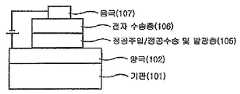
도 1에는 기판(101) 위에 양극(102), 발광층(105) 및 음극(107)이 순차적으로 적층된 유기 발광 소자의 구조가 예시되어 있다. 이와 같은 구조에 있어서, 상기 화학식 1의 화합물은 상기 발광층(105)에 포함될 수 있다.FIG. 1 illustrates a structure of an organic light emitting device in which an anode 102, a light emitting layer 105, and a cathode 107 are sequentially stacked on a substrate 101. In such a structure, the compound of Formula 1 may be included in the light emitting layer 105.
도 2에는 기판(101) 위에 양극(102), 정공 주입/정공 수송 및 발광층(105), 전자 수송층(106) 및 음극(107)이 순차적으로 적층된 유기 발광 소자의 구조가 예시되어 있다. 이와 같은 구조에 있어서, 상기 화학식 1의 화합물은 정공 주입/정공 수송 및 발광층(105)에 포함될 수 있다.2 illustrates a structure of an organic light emitting device in which an anode 102, a hole injection / hole transporting and light emitting layer 105, an electron transporting layer 106, and a cathode 107 are sequentially stacked on a substrate 101. In such a structure, the compound of Formula 1 may be included in the hole injection / hole transporting and light emitting layer 105.
도 3에는 기판(101), 양극(102), 정공 주입층(103), 정공 수송 및 발광 층(105), 전자 수송층(106) 및 음극(107)이 순차적으로 적층된 유기 발광 소자의 구조가 예시되어 있다. 이와 같은 구조에 있어서, 상기 화학식 1의 화합물은 정공 주입/정공 수송 및 발광층(105)에 포함될 수 있다.3 illustrates a structure of an organic light emitting device in which a substrate 101, an anode 102, a hole injection layer 103, a hole transport and emission layer 105, an electron transport layer 106, and a cathode 107 are sequentially stacked. Is illustrated. In such a structure, the compound of Formula 1 may be included in the hole injection / hole transporting and light emitting layer 105.
도 4에는 기판(101), 양극(102), 정공 주입층(103), 정공 수송층(104), 전자 수송 및 발광층(105) 및 음극(107)이 순차적으로 적층된 유기 발광 소자의 구조가 예시되어 있다. 이와 같은 구조에 있어서, 상기 화학식 1의 화합물은 전자 수송 및 발광층(105)에 포함될 수 있다.4 shows a structure of an organic light emitting device in which a substrate 101, an anode 102, a hole injecting layer 103, a hole transporting layer 104, an electron transporting and emitting layer 105, and a cathode 107 are sequentially laminated. . In such a structure, the compound of Formula 1 may be included in the electron transporting and light emitting layer 105.
예컨대, 본 발명에 따른 유기 발광 소자는 스퍼터링(sputtering)이나 전자빔 증발(e-beam evaporation)과 같은 PVD(physical vapor deposition) 방법을 이용하여, 기판 상에 금속 또는 전도성을 가지는 금속 산화물 또는 이들의 합금을 증착시켜 양극을 형성하고, 그 위에 정공 주입층, 정공 수송층, 발광층 및 전자 수송층을 포함하는 유기물층을 형성한 후, 그 위에 음극으로 사용할 수 있는 물질을 증착시킴으로써 제조될 수 있다. 이와 같은 방법 외에도, 기판 상에 음극 물질부터 유기물층, 양극 물질을 차례로 증착시켜 유기 발광 소자를 만들 수도 있다.For example, the organic light emitting device according to the present invention may be formed by using a PVD (physical vapor deposition) method such as sputtering or e-beam evaporation to form a metal oxide or a metal oxide having conductivity on the substrate, To form an anode, an organic material layer including a hole injection layer, a hole transporting layer, a light emitting layer, and an electron transporting layer is formed on the anode, and a material which can be used as a cathode is deposited thereon. In addition to such a method, an organic light emitting device may be formed by sequentially depositing a cathode material, an organic material layer, and a cathode material on a substrate.
상기 유기물층은 정공 주입층, 정공 수송층, 발광층 및 전자 수송층 등을 포함하는 다층 구조일 수도 있으나, 이에 한정되지 않고 단층 구조일 수 있다. 또한, 상기 유기물층은 다양한 고분자 소재를 사용하여 증착법이 아닌 용매 공정(solvent process), 예컨대 스핀 코팅, 딥 코팅, 닥터 블레이딩, 스크린 프린팅, 잉크젯 프린팅 또는 열 전사법 등의 방법에 의하여 더 적은 수의 층으로 제조할 수 있다.The organic material layer may have a multi-layer structure including a hole injection layer, a hole transport layer, a light emitting layer, and an electron transport layer, but is not limited thereto and may have a single layer structure. The organic material layer may be formed using a variety of polymeric materials by a method such as a solvent process such as spin coating, dip coating, doctor blading, screen printing, inkjet printing, Layer.
상기 양극 물질로는 통상 유기물층으로 정공 주입이 원활할 수 있도록 일함 수가 큰 물질이 바람직하다. 본 발명에서 사용될 수 있는 양극 물질의 구체적인 예로는 바나듐, 크롬, 구리, 아연, 금과 같은 금속 또는 이들의 합금; 아연 산화물, 인듐 산화물, 인듐주석 산화물(ITO), 인듐아연 산화물(IZO)과 같은 금속 산화물; ZnO : Al 또는 SnO2 : Sb와 같은 금속과 산화물의 조합; 폴리(3-메틸화합물의), 폴리[3,4-(에틸렌-1,2-디옥시)화합물의](PEDT), 폴리피롤 및 폴리아닐린과 같은 전도성 고분자 등이 있으나, 이들에만 한정되는 것은 아니다.As the anode material, a material having a large work function is usually preferred to facilitate hole injection into the organic material layer. Specific examples of the cathode material that can be used in the present invention include metals such as vanadium, chromium, copper, zinc, and gold, or alloys thereof; Metal oxides such as zinc oxide, indium oxide, indium tin oxide (ITO), and indium zinc oxide (IZO); ZnO: Al or SnO2: a combination of a metal and an oxide such as Sb; Conductive polymers such as poly (3-methyl compounds), poly [3,4- (ethylene-1,2-dioxy) compounds] (PEDT), polypyrrole and polyaniline.
상기 음극 물질로는 통상 유기물층으로 전자 주입이 용이하도록 일함수가 작은 물질인 것이 바람직하다. 음극 물질의 구체적인 예로는 마그네슘, 칼슘, 나트륨, 칼륨, 티타늄, 인듐, 이트륨, 리튬, 가돌리늄, 알루미늄, 은, 주석 및 납과 같은 금속 또는 이들의 합금; LiF/Al 또는 LiO2/Al과 같은 다층 구조 물질 등이 있으나, 이들에만 한정되는 것은 아니다.The negative electrode material is preferably a material having a small work function to facilitate electron injection into the organic material layer. Specific examples of the negative electrode material include metals such as magnesium, calcium, sodium, potassium, titanium, indium, yttrium, lithium, gadolinium, aluminum, silver, tin and lead or alloys thereof; Layer structure materials such as LiF / Al or LiO2 / Al, but are not limited thereto.
상기 정공 주입 물질로는 낮은 전압에서 양극으로부터 정공을 잘 주입 받을 수 있는 물질로서, 정공 주입 물질의 HOMO(highest occupied molecular orbital)가 양극 물질의 일함수와 주변 유기물층의 HOMO 사이인 것이 바람직하다. 정공 주입 물질의 구체적인 예로는 금속 포피린(porphyrine), 올리고티오펜, 아릴아민 계열의 유기물, 헥사니트릴헥사아자트리페닐렌 계열의 유기물, 퀴나크리돈(quinacridone) 계열의 유기물, 페릴렌(perylene) 계열의 유기물, 안트라퀴논 및 폴리아닐린과 폴리화합물의 계열의 전도성 고분자 등이 있으나, 이들에만 한정되는 것은 아니다.As the hole injecting material, it is preferable that the highest occupied molecular orbital (HOMO) of the hole injecting material is between the work function of the anode material and the HOMO of the surrounding organic layer. Specific examples of the hole injecting material include metal porphyrine, oligothiophene, arylamine-based organic materials, hexanitrile hexaazatriphenylene-based organic materials, quinacridone-based organic materials, perylene , An anthraquinone, and a conductive polymer of polyaniline and a poly-compound, but the present invention is not limited thereto.
상기 정공 수송 물질로는 양극이나 정공 주입층으로부터 정공을 수송받아 발 광층으로 옮겨줄 수 있는 물질로 정공에 대한 이동성이 큰 물질이 적합하다. 구체적인 예로는 아릴아민 계열의 유기물, 전도성 고분자, 및 공액 부분과 비공액 부분이 함께 있는 블록 공중합체 등이 있으나, 이들에만 한정되는 것은 아니다.As the hole transporting material, a material capable of receiving holes from the anode or the hole injection layer and transferring the holes to the light emitting layer is suitable. Specific examples include arylamine-based organic materials, conductive polymers, and block copolymers having a conjugated portion and a non-conjugated portion together, but are not limited thereto.
상기 발광 물질로는 정공 수송층과 전자 수송층으로부터 정공과 전자를 각각 수송받아 결합시킴으로써 가시광선 영역의 빛을 낼 수 있는 물질로서, 형광이나 인광에 대한 양자 효율이 좋은 물질이 바람직하다. 구체적인 예로는 8-히드록시-퀴놀린 알루미늄 착물(Alq3); 카르바졸 계열 화합물; 이량체화 스티릴(dimerized styryl) 화합물; BAlq; 10-히드록시벤조 퀴놀린-금속 화합물; 벤족사졸, 벤즈티아졸 및 벤즈이미다졸 계열의 화합물; 폴리(p-페닐렌비닐렌)(PPV) 계열의 고분자; 스피로(spiro) 화합물; 폴리플루오렌, 루브렌 등이 있으나, 이들에만 한정되는 것은 아니다.The light emitting material is preferably a material capable of emitting light in the visible light region by transporting and receiving holes and electrons from the hole transporting layer and the electron transporting layer, respectively, and having good quantum efficiency for fluorescence or phosphorescence. Specific examples include 8-hydroxy-quinoline aluminum complex (Alq3 ); Carbazole-based compounds; Dimerized styryl compounds; BAlq; 10-hydroxybenzoquinoline-metal compounds; Compounds of the benzoxazole, benzothiazole and benzimidazole series; Polymers of poly (p-phenylenevinylene) (PPV) series; Spiro compounds; Polyfluorene, rubrene, and the like, but are not limited thereto.
상기 전자 수송 물질로는 음극으로부터 전자를 잘 주입 받아 발광층으로 옮겨줄 수 있는 물질로서, 전자에 대한 이동성이 큰 물질이 적합하다. 구체적인 예로는 8-히드록시퀴놀린의 Al 착물; Alq3를 포함한 착물; 유기 라디칼 화합물; 히드록시플라본-금속 착물 등이 있으나, 이들에만 한정되는 것은 아니다.As the electron transporting material, a material capable of transferring electrons from the cathode well into the light emitting layer, which is suitable for electrons, is suitable. Specific examples include an Al complex of 8-hydroxyquinoline; Complexes containing Alq3 ; Organic radical compounds; Hydroxyflavone-metal complexes, and the like, but are not limited thereto.
본 발명에 따른 유기 발광 소자는 사용되는 재료에 따라 전면 발광형, 후면 발광형 또는 양면 발광형일 수 있다.The organic light emitting device according to the present invention may be a front emission type, a back emission type, or a both-sided emission type, depending on the material used.
본 발명에 따른 화합물은 유기 태양 전지, 유기 감광체, 유기 트랜지스터 등을 비롯한 유기 전자 소자에서도 유기 발광 소자에 적용되는 것과 유사한 원리로 작용할 수 있다.The compound according to the present invention may also operate on a principle similar to that applied to organic light emitting devices in organic electronic devices including organic solar cells, organic photoconductors, organic transistors, and the like.
따라서, 상기 유기 전자 소자는 유기 발광 소자, 유기 인광 소자, 유기 태양 전지, 유기 감광체(OPC) 및 유기 트랜지스터로 이루어진 군에서 선택될 수 있다.Accordingly, the organic electronic device may be selected from the group consisting of an organic light emitting device, an organic phosphor device, an organic solar cell, an organic photoconductor (OPC), and an organic transistor.
이하, 실시예를 통하여 본 발명의 화학식 1로 표시되는 화합물들의 제조방법 및 이들을 이용한 유기 전자 소자의 제조방법 및 성능에 대하여 구체적으로 설명한다. 그러나, 하기 실시예는 설명을 위한 것이며, 본 발명의 범위가 하기 실시예에 의하여 한정되는 것은 아니다.Hereinafter, the method for preparing the compound represented by the formula (1) of the present invention, the method for producing the organic electronic device using the same, and the performance will be described in detail. However, the following examples are for illustrative purposes only, and the scope of the present invention is not limited by the following examples.
실시예에 있어서 평가 방법은 하기와 같다.The evaluation method in the examples is as follows.
1. 구동전압: Kethley 236(source measure unit)을 사용하여 측정1. Driving voltage: measured using Kethley 236 (source measure unit)
2. 전류효율: SpectraScan Pr-650을 사용하여 측정2. Current efficiency: measured using SpectraScan Pr-650
3. 색좌표: SpectraScan Pr-650을 사용하여 측정3. Color Coordinates: Measured using SpectraScan Pr-650
본 발명에 따른 화학식 1로 표시되는 화합물은 일반적으로 다단계 화학 반응으로 제조될 수 있다. 즉, 일부 중간체 화합물이 먼저 제조되고, 그 중간체 화합물들로부터 화학식 1의 화합물이 제조된다. 예증적인 중간체 화합물들은 하기 합성예에 나타낸 화합물들이다.The compound represented by formula (1) according to the present invention can be generally prepared by a multistage chemical reaction. That is, some of the intermediate compounds are first prepared, and the compounds of formula (1) are prepared from the intermediate compounds. Exemplary intermediate compounds are the compounds shown in the synthesis examples below.
이하, 본 발명의 이해를 돕기 위하여 바람직한 실시예를 제시한다. 그러나, 하기의 실시예는 본 발명을 예시하기 위한 것이며, 이에 의하여 본 발명의 범위가 한정되는 것은 아니다.Hereinafter, preferred embodiments of the present invention will be described in order to facilitate understanding of the present invention. However, the following examples are intended to illustrate the invention and are not intended to limit the scope of the invention.
<<실시예Example>>
<<합성예Synthetic example 1> 1>

1) 화합물 1B의 제조1) Preparation of Compound 1B
상기 화합물 1A [4,4,5,5-tetramethyl-2-(1-(4,4,5,5-tetramethyl-1,3,2-dioxaborolan-2-yl)pyren-6-yl)-1,3,2-dioxaborolane](22.7 g, 50 mmol), 1-bromo-2-nitrobenzene(21.2 g, 105 mmol)을 테트라하이드로퓨란(500 mL)에 완전히 녹인 후, 2M 탄산칼륨 수용액을 첨가하고, 테트라비스트리페닐포스피노 팔라듐(2.4 g, 2 mmol)을 넣은 후, 10시간 동안 가열 교반하였다. 상온으로 온도를 낮추고, 생성된 용액을 무수 황산마그네슘으로 건조하고, CHCl3/n-Hex으로 재결정하여 상기 화합물 1B인(12.7 g, 수율 57%)을 제조하였다.Compound 1A [4,4,5,5-tetramethyl-2- (1- (4,4,5,5-tetramethyl-1,3,2-dioxaborolan-2-yl) pyren-6-yl) -1 , 3,2-dioxaborolane] (22.7 g, 50 mmol) and 1-bromo-2-nitrobenzene (21.2 g, 105 mmol) were completely dissolved in tetrahydrofuran (500 mL), and then 2M aqueous potassium carbonate was added thereto. Tetrabistriphenylphosphino palladium (2.4 g, 2 mmol) was added thereto, followed by heating and stirring for 10 hours. The temperature was lowered to room temperature, the resulting solution was dried over anhydrous magnesium sulfate, and recrystallized with CHCl3 / n-Hex to prepare the compound 1B (12.7 g, yield 57%).
MS: [M+H]+= 445MS: [M + H]+ = 445
2) 화합물 1C의 제조2) Preparation of Compound 1C
상기 1)에서 합성한 화합물 1B(12.7 g, 28.57 mmol), PPh3(37.6 g. 143.2 mmol)를 질소 분위기하에서 무수 1,2-dichlorobenzene(o-DCB)(200 mL)를 넣고, 160 ℃에서 가열하였다. 약 14시간 후 반응온도를 상온으로 떨어뜨린 후 형성된 고체를 여과하고 용매인 o-DCB를 진공증류하였다. 반응 혼합물에 methylene chloride를 가한 후 EtOH을 가해 침전을 형성시켰다. 노르말 헥산으로 POPPh3을 제거한 후 에탄올에서 재결정하여 주황색 고체 화합물 1C(4.7 g, 수율 43 %)를 제조하였다.Compound 1B (12.7 g, 28.57 mmol) and PPh3 (37.6 g. 143.2 mmol) synthesized in 1) were added anhydrous 1,2-dichlorobenzene (o-DCB) (200 mL) under nitrogen atmosphere at 160 ° C. Heated. After about 14 hours, the reaction temperature was lowered to room temperature, the solid formed was filtered, and the solvent o-DCB was distilled under vacuum. Methylene chloride was added to the reaction mixture, followed by addition of EtOH to form a precipitate. After removing POPPh3 with normal hexane and recrystallization in ethanol to give an orange solid compound 1C (4.7 g, 43% yield).
MS: [M+H]+= 381MS: [M + H]+ = 381
<<합성예Synthetic example 2> 2>

1) 화합물 2B의 제조1) Preparation of compound 2B
화합물 1B(8.9 g, 20.0 mmol)를 클로로포름(120 mL)에 녹이고, N-브로모숙신이미드(7.8 g, 44 mmol)를 첨가한 후, 7시간 동안 상온에서 교반하였다. 반응 용액에 증류수를 가하여 반응을 종료시키고 유기층을 추출하였다. 반응액을 농축시키고 톨루엔으로 2회 재결정하여 화학식 2B(6.7 g, 수율 56 %)를 얻었다.Compound 1B (8.9 g, 20.0 mmol) was dissolved in chloroform (120 mL), and N-bromosuccinimide (7.8 g, 44 mmol) was added, followed by stirring at room temperature for 7 hours. Distilled water was added to the reaction solution to terminate the reaction, and the organic layer was extracted. The reaction solution was concentrated and recrystallized twice with toluene to obtain the formula 2B (6.7 g, yield 56%).
MS: [M+H]+= 602MS: [M + H] <+ > = 602
2) 화합물 2C의 제조2) Preparation of compound 2C
상기 1)에서 합성한 화합물 2B(6.7 g, 11.2 mmol), PPh3(9.4 g. 35.82 mmol)를 질소 분위기하에서 무수 1,2-dichlorobenzene(o-DCB)(100 mL)를 넣고, 160 ℃에서 가열하였다. 약 9시간 후 반응온도를 상온으로 떨어뜨린 후 형성된 고체를 여과하고 용매인 o-DCB를 진공증류하였다. 반응 혼합물에 methylene chloride를 가한 후 EtOH을 가해 침전을 형성시켰다. 노르말 헥산으로 POPPh3을 제거한 후 에탄올에서 재결정하여 주황색 고체 화합물 2C(2.9 g, 수율 48 %)를 제조하였다.Compound 2B (6.7 g, 11.2 mmol) and PPh3 (9.4 g. 35.82 mmol) synthesized in 1) were added anhydrous 1,2-dichlorobenzene (o-DCB) (100 mL) in a nitrogen atmosphere at 160 ° C. Heated. After about 9 hours, the reaction temperature was lowered to room temperature, the solid formed was filtered, and the solvent o-DCB was distilled under vacuum. Methylene chloride was added to the reaction mixture, followed by addition of EtOH to form a precipitate. After removing POPPh3 with normal hexane and recrystallized in ethanol to give an orange solid compound 2C (2.9 g, yield 48%).
MS: [M+H]+= 538MS: [M + H]+ = 538
<<합성예Synthetic example 3> 3>

1) 화합물 3B의 제조1) Preparation of Compound 3B
1,6-dibromopyrrene(7.2 g, 20.0 mmol)을 질소 분위기 하에서 무수 THF(100 mL)를 넣고, -78 ℃로 반응 온도를 유지하였다. n-BuLi(2.5 M in HEX, 9.6 mL, 24 mmol)을 반응 용액에 적가하였다. 약 40분 동안 교반한 후 반응 혼합 용액에 chlorotrimethylsilane(3.3 g, 30 mmol)을 가해 교반하였다. 약 1시간 후 상온으로 승온시키고 3시간 동안 교반하였다. 반응 혼합물에 수용성 염화암모늄 용액을 가한 후 THF 층을 분리하였다. 무수 황산 마그네슘으로 유기 층을 건조시킨 후, 에틸에 테르를 가해 교반시켜 고체화합물 4B(4.2 g, 61 %)를 제조하였다.1,6-dibromopyrrene (7.2 g, 20.0 mmol) was put in anhydrous THF (100 mL) under nitrogen atmosphere, and the reaction temperature was maintained at -78 ° C. n-BuLi (2.5 M in HEX, 9.6 mL, 24 mmol) was added dropwise to the reaction solution. After stirring for about 40 minutes, chlorotrimethylsilane (3.3 g, 30 mmol) was added to the reaction mixture and stirred. After about 1 hour it was raised to room temperature and stirred for 3 hours. Aqueous ammonium chloride solution was added to the reaction mixture, and the THF layer was separated. After drying the organic layer with anhydrous magnesium sulfate, ethyl ether was added and stirred to prepare a solid compound 4B (4.2 g, 61%).
MS: [M+H]+= 347MS: [M + H]+ = 347
2) 화합물 3B-1의 제조2) Preparation of Compound 3B-1
화합물 3B(4.2 g, 12.2 mmol)를 클로로포름(120 mL)에 녹이고, N-브로모 숙신이미드(4.3 g, 24.4 mmol)를 첨가한 후, 5시간 동안 상온에서 교반하였다. 반응 용액에 증류수를 가하여 반응을 종료시키고 유기층을 추출하였다. 반응액을 농축시키고 톨루엔으로 재결정하여 화학식 3B-1(4.1 g, 수율 67 %)를 얻었다.Compound 3B (4.2 g, 12.2 mmol) was dissolved in chloroform (120 mL), and N-bromo succinimide (4.3 g, 24.4 mmol) was added, followed by stirring at room temperature for 5 hours. Distilled water was added to the reaction solution to terminate the reaction, and the organic layer was extracted. The reaction solution was concentrated and recrystallized with toluene to obtain the formula 3B-1 (4.1 g, 67% yield).
MS: [M+H]+= 504MS: [M + H]+ = 504
3) 화합물 3B-2의 제조3) Preparation of Compound 3B-2
화합물 3B-1(5.4 g, 10.7 mmol), 비스(피나콜라토)디보론(2.75 g, 10.9 mmol) 및 아세트산 칼륨(2.89 g, 29.4 mmol)을 디옥산(50 mL)에 현탁시켰다. 상기 현탁액에 팔라듐(디페닐포스피노페로센)클로라이드(0.24 g, 3 mol%)를 가하였다. 혼합물을 약 6시간 동안 80 ℃에서 교반하고, 실온으로 냉각하였다. 상기 혼합물을 물(50 mL)로 희석하고 디클로로메탄(3 x 50 mL)으로 추출하였다. 유기 추출물을 황산 마그네슘 상에서 건조하고 진공 내에서 농축하였다. 조 생성물을 에탄올로 세척하고 진공 내에서 건조하여 보레이트 화합물 3B-2(5.9 g, 92 %)를 얻었다.Compound 3B-1 (5.4 g, 10.7 mmol), bis (pinacolato) diboron (2.75 g, 10.9 mmol) and potassium acetate (2.89 g, 29.4 mmol) were suspended in dioxane (50 mL). Palladium (diphenylphosphinoferrocene) chloride (0.24 g, 3 mol%) was added to the suspension. The mixture was stirred at 80 ° C. for about 6 hours and cooled to room temperature. The mixture was diluted with water (50 mL) and extracted with dichloromethane (3 x 50 mL). The organic extract was dried over magnesium sulfate and concentrated in vacuo. The crude product was washed with ethanol and dried in vacuo to yield borate compound 3B-2 (5.9 g, 92%).
MS: [M+H]+= 599MS: [M + H] <+ > = 599
4) 화합물 3B-3의 제조4) Preparation of Compound 3B-3
합성예 1의 화합물 1B의 제조에 있어서, 화합물 1A 대신에 화합물 3B-2(5.9 g, 9.9 mmol)을 사용한 것을 제외하고 동일한 방법으로 화합물 3B-3(3.9 g, 67 %)을 제조하였다.In the preparation of Compound 1B of Synthesis Example 1, Compound 3B-3 (3.9 g, 67%) was prepared in the same manner except that Compound 3B-2 (5.9 g, 9.9 mmol) was used instead of Compound 1A.
MS: [M+H]+= 589MS: [M + H] <+ > = 589
5) 화합물 3C의 제조5) Preparation of Compound 3C
합성예 1의 화합물 1C의 제조에 있어서, 화합물 1B 대신에 화합물 3B-3(3.9 g, 6.6 mmol)을 사용한 것을 제외하고 동일한 방법으로 화합물 3C(1.7 g, 48 %)를 제조하였다.In preparing Compound 1C of Synthesis Example 1, Compound 3C (1.7 g, 48%) was prepared in the same manner except that Compound 3B-3 (3.9 g, 6.6 mmol) was used instead of Compound 1B.
MS: [M+H]+= 525MS: [M + H] <+ > = 525
<<합성예Synthetic example 4> 4>

1) 화합물 4B의 제조1) Preparation of Compound 4B
상기 합성예 1-1의 화합물 3B의 제조에 있어서, 화합물 chlorotrimethylsilane 대신 화합물 Methyliodide를 사용한 것을 제외하고는 동일한 방법으로 제조하여 화합물 4B를 제조하였다.In preparing Compound 3B of Synthesis Example 1-1, Compound 4B was prepared by the same method except that Compound Methyliodide was used instead of Compound Chlorotrimethylsilane.
MS: [M+H]+= 231MS: [M + H]+ = 231
2) 화합물 4B-1의 제조2) Preparation of Compound 4B-1
상기 합성예 2의 화합물 3B-1의 제조에 있어서, 화합물 3B 대신 화합물 4B를 사용한 것을 제외하고는 동일한 방법으로 제조하여 화합물 4B-1을 제조하였다.In the preparation of Compound 3B-1 of Synthesis Example 2, the compound 4B-1 was prepared by the same method except that the compound 4B was used instead of the compound 3B.
MS: [M+H]+= 388MS: [M + H]+ = 388
3) 화합물 4B-2의 제조3) Preparation of Compound 4B-2
상기 합성예 2의 화합물 3B-2의 제조에 있어서, 화합물 3B-1 대신 화합물 4B-1을 사용한 것을 제외하고는 동일한 방법으로 제조하여 화합물 4B-2를 제조하였다.In the preparation of Compound 3B-2 of Synthesis Example 2, the compound 4B-2 was prepared by the same method except that the compound 4B-1 was used instead of the compound 3B-1.
MS: [M+H]+= 483MS: [M + H]+ = 483
4) 화합물 4B-3의 제조4) Preparation of Compound 4B-3
상기 합성예 2의 화합물 3B-3의 제조에 있어서, 화합물 3B-2 대신 화합물 4B-2를 사용한 것을 제외하고는 동일한 방법으로 제조하여 화합물 4B-3을 제조하였다.In preparing Compound 3B-3 of Synthesis Example 2, Compound 4B-3 was prepared by the same method except that Compound 4B-2 was used instead of Compound 3B-2.
MS: [M+H]+= 473MS: [M + H]+ = 473
5) 화합물 4C의 제조5) Preparation of Compound 4C
상기 합성예 2의 화합물 3C의 제조에 있어서, 화합물 3B-3 대신 화합물 4B-3을 사용한 것을 제외하고는 동일한 방법으로 제조하여 화합물 4C를 제조하였다.In preparing Compound 3C of Synthesis Example 2, Compound 4C was prepared by the same method except that Compound 4B-3 was used instead of Compound 3B-3.
MS: [M+H]+= 409MS: [M + H]+ = 409
<<제조예Manufacturing example>>
<<제조예Manufacturing example 1> 화합물 1-2-2의 제조 1> Preparation of Compound 1-2-2

(4-bromophenyl)trimethylsilane(10.1 g, 44.0 mmol), 화학식 1C(7.6 g, 20.0 mmol)을 자일렌 200 mL에 용해시키고, 나트륨-터셔리-부톡사이드(4.0 g, 40 mmol), Pd[P(t-Bu)3]2 0.1 g(0.2 mmol)을 첨가한 후, 5시간 동안 질소 기류 하에서 환류하였다. 반응 용액에 증류수를 넣고 반응을 종료시키고 유기층을 추출하였다. 노르말-헥산/CHCl3 용매로 재결정하여 화합물 1-2-2(8.4 g, 수율 62%)를 제조하였다.(4-bromophenyl) trimethylsilane (10.1 g, 44.0 mmol), Formula 1C (7.6 g, 20.0 mmol) was dissolved in 200 mL of xylene, sodium-tertiary-butoxide (4.0 g, 40 mmol), Pd [P (t-Bu)3 ]2 0.1 g (0.2 mmol) was added and then refluxed under nitrogen stream for 5 hours. Distilled water was added to the reaction solution, the reaction was terminated, and the organic layer was extracted. Compound 1-2-2 (8.4 g, yield 62%) was prepared by recrystallization with a normal-hexane / CHCl3 solvent.
MS: [M+H]+ =677MS: [M + H]+ = 677
<<제조예Manufacturing example 2> 화합물 1-2-5의 제조 2> Preparation of Compound 1-2-5

상기 제조예 1의 화합물 1-2-2의 제조예에 있어서, (4-bromophenyl)trimethylsilane 대신에 1-bromo-3-methylbenzene(4.4 g, 26.0 mmol)을, 화합물 1C 대신에 화합물 2C(4.2 g, 11.0 mmol)를 사용한 것을 제외하고 동일한 방법으로 반응시켜 화합물 1-2-5(4.3 g, 수율 70%)을 제조하였다.In the preparation of compound 1-2-2 of Preparation Example 1, 1-bromo-3-methylbenzene (4.4 g, 26.0 mmol) in place of (4-bromophenyl) trimethylsilane, and Compound 2C (4.2 g in place of Compound 1C , 11.0 mmol) was reacted in the same manner to prepare a compound 1-2-5 (4.3 g, yield 70%).
MS: [M+H]+ =561MS: [M + H]+ = 561
<<제조예Manufacturing example 3> 화합물 1-2-27의 제조 3> Preparation of Compound 1-2-27

상기 제조예 1의 화합물 1-2-2의 제조예에 있어서, (4- bromophenyl)trimethylsilane 대신에 4-fluoro-1-bromobenzene(7.0 g, 40.0 mmol)을 사용하고, 화합물 1C(6.8 g, 18.0 mmol)를 사용한 것을 제외하고 동일한 방법으로 반응시켜 화합물 1-2-27(6.7 g, 수율 65%)을 제조하였다.In Preparation Example of Compound 1-2-2 of Preparation Example 1, 4-fluoro-1-bromobenzene (7.0 g, 40.0 mmol) was used instead of (4-bromophenyl) trimethylsilane, and Compound 1C (6.8 g, 18.0) was used. Compound 1-2-27 (6.7 g, yield 65%) was prepared in the same manner except for the use of mmol).
MS: [M+H]+ =569MS: [M + H]+ = 569
<<제조예Manufacturing example 4> 화합물 1-2-15의 제조 4> Preparation of Compound 1-2-15

상기 제조예 1의 화합물 1-2-2의 제조예에 있어서, (4-bromophenyl)trimethylsilane 대신에 bromobenzene(6.9 g, 44 mmol)을 사용하고, 화합물 3C(10.5 g, 20.0 mmol)를 사용한 것을 제외하고 동일한 방법으로 반응시켜 화합물 1-2-15(4.9 g, 수율 36%)을 제조하였다.In Preparation Example of Compound 1-2-2 of Preparation Example 1, except that instead of (4-bromophenyl) trimethylsilane, bromobenzene (6.9 g, 44 mmol) was used and compound 3C (10.5 g, 20.0 mmol) was used. And reacted in the same manner to give compound 1-2-15 (4.9 g, yield 36%).
MS: [M+H]+ =677MS: [M + H]+ = 677
<<제조예Manufacturing example 5> 화합물 1-2-29의 제조 5> Preparation of Compound 1-2-29

상기 제조예 1의 화합물 1-2-2의 제조예에 있어서, (4-bromophenyl)trimethylsilane 대신에 4-fluoro-1-bromobenzene(7.0 g, 40.0 mmol)을 사용하고, 화합물 3C(9.4 g, 18.0 mmol)를 사용한 것을 제외하고 동일한 방법으로 반응시켜 화합물 1-2-29(5.9 g, 수율 46%)를 제조하였다.In Preparation Example of Compound 1-2-2 of Preparation Example 1, 4-fluoro-1-bromobenzene (7.0 g, 40.0 mmol) was used instead of (4-bromophenyl) trimethylsilane, and Compound 3C (9.4 g, 18.0) was used. Compound 1-2-29 (5.9 g, yield 46%) was prepared in the same manner except for the use of mmol).
MS: [M+H]+ =714MS: [M + H]+ = 714
<<제조예Manufacturing example 6> 화합물 1-2-13의 제조 6> Preparation of Compound 1-2-13

상기 제조예 1의 화합물 1-2-2의 제조예에 있어서, (4-bromophenyl)trimethylsilane 대신에 (3-bromophenyl)trimethylsilane(5.5 g, 24.2 mmol)을, 화합물 1C 대신에 화합물 3C(4.2 g, 11.0 mmol)를 사용한 것을 제외하고 동일한 방법으로 반응시켜 화합물 1-2-13(4.4 g, 수율 49%)를 제조하였다.In the Preparation Example of Compound 1-2-2 of Preparation Example 1, instead of (4-bromophenyl) trimethylsilane (3-bromophenyl) trimethylsilane (5.5 g, 24.2 mmol) was replaced with Compound 3C (4.2 g, Compound 1-2-13 (4.4 g, 49% yield) was prepared by the same method except that 11.0 mmol) was used.
MS: [M+H]+ =821MS: [M + H]+ = 821
<<제조예Manufacturing example 7> 화합물 1-2-16의 제조 7> Preparation of Compound 1-2-16

상기 제조예 1의 화합물 1-2-2의 제조예에 있어서, (4-bromophenyl)trimethylsilane 대신에 bromobenzene(4.9 g, 31.2 mmol)을, 화합물 1C 대신에 화합물 4C(5.8 g, 14.2 mmol)를 사용한 것을 제외하고 동일한 방법으로 반응시켜 화합물 1-2-16(5.3 g, 수율 67%)을 제조하였다.In the preparation example of compound 1-2-2 of Preparation Example 1, instead of (4-bromophenyl) trimethylsilane, bromobenzene (4.9 g, 31.2 mmol) was used, and instead of compound 1C, compound 4C (5.8 g, 14.2 mmol) was used. Compound 1-2-16 (5.3 g, yield 67%) was prepared by reaction in the same manner except for the same.
MS: [M+H]+ =561MS: [M + H]+ = 561
<<제조예Manufacturing example 8> 화합물 1-2-33의 제조 8> Preparation of Compound 1-2-33

상기 합성예 2에서 제조한 화합물 2C(8.1 g, 15.0 mmol), phenylboronic acid(6.6 g, 54.0 mmol)를 테트라하이드로퓨란(120 mL)에 완전히 녹인 후, 2M 탄산칼륨 수용액을 첨가하고, 테트라비스트리페닐포스피노 팔라듐(0.35 g, 0.3 mol)을 넣은 후, 10시간 동안 가열 교반하였다. 상온으로 온도를 낮추고, 생성된 고체를 진공 오븐에서 건조하고, CH2Cl2로 재결정하여 상기 화합물 5C(4.6 g, 수율 57 %)를 제조하였다.Compound 2C (8.1 g, 15.0 mmol) and phenylboronic acid (6.6 g, 54.0 mmol) prepared in Synthesis Example 2 were completely dissolved in tetrahydrofuran (120 mL), followed by addition of an aqueous 2M potassium carbonate solution, followed by tetrabistri Phenylphosphino palladium (0.35 g, 0.3 mol) was added thereto, followed by heating and stirring for 10 hours. The temperature was lowered to room temperature, the resulting solid was dried in a vacuum oven, and recrystallized with CH2 Cl2 to prepare the compound 5C (4.6 g, yield 57%).
MS: [M+H]+ =533MS: [M + H]+ = 533
상기 제조예 1의 화합물 1-2-2의 제조예에 있어서, (4-bromophenyl)trimethylsilane 대신에 bromobenzene(4.9 g, 31.2 mmol)을, 화합물 1C 대신에 화합물 5C(5.8 g, 14.2 mmol)를 사용한 것을 제외하고 동일한 방법으로 반응시켜 화합물 1-2-33(5.3 g, 수율 67%)을 제조하였다.In the preparation example of compound 1-2-2 of Preparation Example 1, using bromobenzene (4.9 g, 31.2 mmol) in place of (4-bromophenyl) trimethylsilane, and compound 5C (5.8 g, 14.2 mmol) in place of compound 1C Compound 1-2-33 (5.3 g, yield 67%) was prepared by the same method except for the same reaction.
MS: [M+H]+ =684MS: [M + H]+ = 684
<<제조예Manufacturing example 9> 화합물 1-2-31의 제조 9> Preparation of Compound 1-2-31

상기 합성예 2에서 제조한 화합물 2C(4.3 g, 7.0 mmol), 5-methylthiophene-2-boronic acid(3.8 g, 27.0 mmol)를 테트라하이드로퓨란(80 mL)에 완전히 녹인 후, 2M 탄산칼륨 수용액을 첨가하고, 테트라비스트리페닐포스피노 팔라듐(0.16 g, 0.14 mol)을 넣은 후, 10시간 동안 가열 교반하였다. 상온으로 온도를 낮추고, 생성된 고체를 진공 오븐에서 건조하고, CH2Cl2로 재결정하여 상기 화합물 6C(1.9 g, 수율 48 %)를 제조하였다.Compound 2C (4.3 g, 7.0 mmol) and 5-methylthiophene-2-boronic acid (3.8 g, 27.0 mmol) prepared in Synthesis Example 2 were completely dissolved in tetrahydrofuran (80 mL), followed by 2M aqueous potassium carbonate solution. Tetrabistriphenylphosphino palladium (0.16 g, 0.14 mol) was added thereto, followed by heating and stirring for 10 hours. The temperature was lowered to room temperature, the resulting solid was dried in a vacuum oven and recrystallized with CH2 Cl2 to prepare the compound 6C (1.9 g, yield 48%).
MS: [M+H]+ =573MS: [M + H] <+ > = 573
상기 제조예 1의 화합물 1-2-2의 제조예에 있어서, (4-bromophenyl)trimethylsilane 대신에 bromobenzene(1.3 g, 31.2 mmol)을, 화합물 1C 대신에 화합물 6C(5.8 g, 14.2 mmol)를 사용한 것을 제외하고 동일한 방법으로 반응시켜 화합물 1-2-31(5.3 g, 수율 67%)을 제조하였다.In the preparation of compound 1-2-2 of Preparation Example 1, using bromobenzene (1.3 g, 31.2 mmol) in place of (4-bromophenyl) trimethylsilane, and compound 6C (5.8 g, 14.2 mmol) in place of compound 1C Compound 1-2-31 (5.3 g, yield 67%) was prepared by the same method except for the same reaction.
MS: [M+H]+ =725MS: [M + H] <+ > = 725
<<비교예Comparative Example 1-1> 1-1>
ITO(indium tin oxide)가 1,500Å의 두께로 박막 코팅된 유리 기판을 세제를 녹인 증류수에 넣고 초음파로 세척하였다. 이때, 세제로는 피셔(Fischer Co.) 사의 제품을 사용하였으며, 증류수로는 밀리포어(Millipore Co.) 사 제품의 필터(Filter)로 2차로 걸러진 증류수를 사용하였다. ITO를 30분간 세척한 후 증류수로 2회 반복하여 초음파 세척을 10분간 진행하였다. 증류수 세척이 끝난 후, 이소프로필알코올, 아세톤, 메탄올의 용제로 초음파 세척을 하고 건조시킨 후 플라즈마 세정기로 수송시켰다. 산소 플라즈마를 이용하여 상기 기판을 5분간 세정한 후 진공 증착기로 기판을 수송시켰다.The glass substrate coated with ITO (indium tin oxide) film with a thickness of 1,500 Å was immersed in distilled water containing detergent and washed with ultrasonic waves. At this time, a product of Fischer Co. was used as a detergent, and distilled water filtered secondly as a filter of Millipore Co. was used as distilled water. The ITO was washed for 30 minutes and then washed twice with distilled water and ultrasonically cleaned for 10 minutes. After washing the distilled water, ultrasonic washing with a solvent of isopropyl alcohol, acetone, methanol, dried and transported to a plasma cleaner. The substrate was cleaned using oxygen plasma for 5 minutes, and then the substrate was transported by a vacuum evaporator.
이렇게 준비된 ITO 투명 전극 위에 헥사니트릴 헥사아자트리페닐렌(hexanitrile hexaazatriphenylene)를 500Å의 두께로 열 진공 증착하여 정공 주입층을 형성하였다. 그 위에 정공을 수송하는 물질인 NPB(400Å)를 진공증착한 후 발광층으로 호스트 H1과 도판트 D1 화합물을 300Å의 두께로 진공 증착하였다.Hexanitrile hexaazatriphenylene was thermally vacuum deposited on the prepared ITO transparent electrode to a thickness of 500 Å to form a hole injection layer. NPB (400 Å), which is a hole transporting material, was vacuum deposited thereon, and a host H1 and a dopant D1 compound were vacuum deposited as a light emitting layer to a thickness of 300 Å.


상기 발광층 위에 화합물 E1를 200Å의 두께로 진공증착하여 전자 주입 및 수송층을 형성하였다. 상기 전자 주입 및 수송층 위에 순차적으로 12Å 두께의 리튬 플루라이드(LiF)와 2,000Å 두께의 알루미늄을 증착하여 음극을 형성하였다. 상기의 과정에서 유기물의 증착속도는 1 Å/sec를 유지하였고, 리튬플루라이드는 0.2 Å/sec, 알루미늄은 3~7 Å/sec의 증착속도를 유지하였다.Compound E1 was vacuum deposited to a thickness of 200 kPa on the light emitting layer to form an electron injection and transport layer. Lithium fluoride (LiF) 12 Å thick and aluminum 2,000 Å thick were sequentially deposited on the electron injection and transport layer to form a cathode. In the above process, the deposition rate of the organic material was maintained at 1 Å / sec, the lithium fluoride was 0.2 Å / sec, and the aluminum was maintained at a deposition rate of 3-7 Å / sec.
<<실험예Experimental Example 1-1> 1-1>
ITO(indium tin oxide)가 1,500Å의 두께로 박막 코팅된 유리 기판을 세제를 녹인 증류수에 넣고 초음파로 세척하였다. 이때, 세제로는 피셔(Fischer Co.) 사의 제품을 사용하였으며, 증류수로는 밀리포어(Millipore Co.) 사 제품의 필터(Filter)로 2차로 걸러진 증류수를 사용하였다. ITO를 30분간 세척한 후 증류수로 2회 반복하여 초음파 세척을 10분간 진행하였다. 증류수 세척이 끝난 후, 이소프로필알코올, 아세톤, 메탄올의 용제로 초음파 세척을 하고 건조시킨 후 플라즈마 세정기로 수송시켰다. 산소 플라즈마를 이용하여 상기 기판을 5분간 세정한 후 진공 증착기로 기판을 수송시켰다.The glass substrate coated with ITO (indium tin oxide) film with a thickness of 1,500 Å was immersed in distilled water containing detergent and washed with ultrasonic waves. At this time, a product of Fischer Co. was used as a detergent, and distilled water filtered secondly as a filter of Millipore Co. was used as distilled water. The ITO was washed for 30 minutes and then washed twice with distilled water and ultrasonically cleaned for 10 minutes. After washing the distilled water, ultrasonic washing with a solvent of isopropyl alcohol, acetone, methanol, dried and transported to a plasma cleaner. The substrate was cleaned using oxygen plasma for 5 minutes, and then the substrate was transported by a vacuum evaporator.
이렇게 준비된 ITO 투명 전극 위에 헥사니트릴 헥사아자트리페닐렌(hexanitrile hexaazatriphenylene)을 500Å의 두께로 열 진공 증착하여 정공 주입층을 형성하였다. 그 위에 정공을 수송하는 물질인 NPB(400Å)를 진공증착한 후 발광층으로 상기 제조예 1-1에서 합성한 화합물 1-2-2를 호스트 화합물로 300Å의 두께로 진공증착하고 그 위에 도판트 D1을 4% 도핑하였다. 상기 발광층 위에 상기 E1을 200Å의 두께로 진공증착하여 전자 주입 및 수송층을 형성하였다. 상기 전자 수송층 위에 순차적으로 12Å 두께의 리튬 플루라이드(LiF)와 2,000Å 두께의 알루미늄을 증착하여 음극을 형성하고 유기 발광 소자를 제조하였다.Hexanitrile hexaazatriphenylene was thermally vacuum deposited to a thickness of 500 kPa on the prepared ITO transparent electrode to form a hole injection layer. NPB (400 kPa), which is a material for transporting holes, was vacuum-deposited, and then compound 1-2-2 synthesized in Preparation Example 1-1 was vacuum-deposited with a host compound at a thickness of 300 kPa as a light emitting layer, and a dopant D1 was deposited thereon. Was doped 4%. The E1 was vacuum deposited to a thickness of 200 kPa on the light emitting layer to form an electron injection and transport layer. 12 전자 of lithium fluoride (LiF) and 2,000 Å of aluminum were deposited on the electron transport layer to form a cathode, thereby manufacturing an organic light emitting device.
상기의 과정에서 유기물의 증착속도는 0.4~0.7 Å/sec를 유지하였고, 음극의 리튬플루라이드는 0.3 Å/sec, 알루미늄은 2 Å/sec의 증착속도를 유지하였으며, 증착시 진공도는 2×10⁻⁷ ~ 5×10⁻⁸ torr를 유지하였다.In the above process, the deposition rate of the organic material was maintained at 0.4˜0.7 Å / sec, the lithium fluoride of the cathode was maintained at 0.3 Å / sec, and the aluminum had a deposition rate of 2 Å / sec.−7 to 5 × 10⁻⁸ torr was maintained.
<<실험예Experimental Example 1-2 내지 1-7> 1-2 to 1-7>
상기 실험예 1-1에서 화합물 1-2-2 대신 상기 제조예 2 내지 제조예 7에서 각각 제조된 화합물을 사용한 것을 제외하고는 동일하게 실험하였다.Except for using the compounds prepared in Preparation Examples 2 to 7 instead of the compound 1-2-2 in Experimental Example 1-1 and was the same experiment.
상기 실험예 1-1 내지 1-7과 같이 각각의 화합물들을 발광 층의 호스트 및 도펀트로 사용하여 제조한 유기 발광 소자를 실험한 결과를 하기 표 1에 나타내었다.As in Experimental Examples 1-1 to 1-7, the results of experimenting with the organic light emitting device manufactured by using the respective compounds as the host and the dopant of the emission layer are shown in Table 1 below.
[표 1][Table 1]

상기 표 1에서 볼 수 있듯이 실험 예 1-1 내지 1-7은 발광층으로 이용될 수 있으며, 적당한 치환체 또는 치환체의 위치에 따라, 다양한 파장대의 발광층에 이용될 수 있다. 특히 알킬기나 티오페닐기, 아릴기와 같은 치환체가 도입된 화합물은 색좌표에서 청색에서 녹색 쪽으로 이동한 빛을 낼 수 있었으며, F나 CN 등으로 치환된 아릴기나, 직접 연결된 경우 또는 실릴기가 도입된 경우는 색좌표에서 볼 수 있듯이 청색 빛을 얻을 수 있었다.As shown in Table 1, Experimental Examples 1-1 to 1-7 may be used as the light emitting layer, and may be used in the light emitting layer of various wavelength bands according to appropriate substituents or positions of the substituents. In particular, compounds in which substituents such as alkyl groups, thiophenyl groups, and aryl groups were introduced could emit light shifted from blue to green in color coordinates, and aryl groups substituted with F or CN, or when directly connected or silyl groups were introduced As can be seen, blue light was obtained.
도 1은 기판(101) 위에 양극(102), 발광층(105) 및 음극(107)이 순차적으로 적층된 유기 발광 소자 구조의 예시이다.1 is an example of an organic light emitting device structure in which an anode 102, a light emitting layer 105, and a cathode 107 are sequentially stacked on a substrate 101.
도 2는 기판(101) 위에 양극(102), 정공 주입/정공 수송 및 발광층(105), 전자 수송층(106) 및 음극(107)이 순차적으로 적층된 유기 발광 소자 구조의 예시이다.2 illustrates an organic light emitting device structure in which an anode 102, a hole injection / hole transport and light emitting layer 105, an electron transport layer 106, and a cathode 107 are sequentially stacked on a substrate 101.
도 3은 기판(101), 양극(102), 정공 주입층(103), 정공 수송 및 발광층(105), 전자 수송층(106) 및 음극(107)이 순차적으로 적층된 유기 발광 소자 구조의 예시이다.3 is an example of an organic light emitting device structure in which a substrate 101, an anode 102, a hole injection layer 103, a hole transport and light emitting layer 105, an electron transport layer 106 and a cathode 107 are sequentially stacked. .
도 4는 기판(101), 양극(102), 정공 주입층(103), 정공 수송층(104), 전자 수송 및 발광층(105) 및 음극(107)이 순차적으로 적층된 유기 발광 소자 구조의 예시이다.4 is an example of an organic light emitting device structure in which a substrate 101, an anode 102, a hole injection layer 103, a hole transport layer 104, an electron transporting and emitting layer 105, and a cathode 107 are sequentially stacked. .
Claims (8)
Translated fromKorean


Priority Applications (1)
| Application Number | Priority Date | Filing Date | Title |
|---|---|---|---|
| KR1020090064540AKR101314383B1 (en) | 2009-07-15 | 2009-07-15 | New compounds and organic electronic device using the same |
Applications Claiming Priority (1)
| Application Number | Priority Date | Filing Date | Title |
|---|---|---|---|
| KR1020090064540AKR101314383B1 (en) | 2009-07-15 | 2009-07-15 | New compounds and organic electronic device using the same |
Publications (2)
| Publication Number | Publication Date |
|---|---|
| KR20110006915A KR20110006915A (en) | 2011-01-21 |
| KR101314383B1true KR101314383B1 (en) | 2013-10-04 |
Family
ID=43613601
Family Applications (1)
| Application Number | Title | Priority Date | Filing Date |
|---|---|---|---|
| KR1020090064540AActiveKR101314383B1 (en) | 2009-07-15 | 2009-07-15 | New compounds and organic electronic device using the same |
Country Status (1)
| Country | Link |
|---|---|
| KR (1) | KR101314383B1 (en) |
Families Citing this family (14)
| Publication number | Priority date | Publication date | Assignee | Title |
|---|---|---|---|---|
| US9169274B2 (en) | 2009-12-21 | 2015-10-27 | Idemitsu Kosan Co., Ltd. | Pyrene derivative and organic electroluminescent element using the same |
| KR20120081539A (en)* | 2011-01-11 | 2012-07-19 | (주)씨에스엘쏠라 | Organic light compound and organic light device using the same |
| KR101881081B1 (en)* | 2011-06-22 | 2018-08-20 | 삼성디스플레이 주식회사 | Heterocyclic compound, organic light-emitting diode comprising the same and flat display device |
| JP6063114B2 (en) | 2011-08-18 | 2017-01-18 | ユー・ディー・シー アイルランド リミテッド | ORGANIC ELECTROLUMINESCENT ELEMENT, ELEMENT MATERIAL, AND LIGHT EMITTING DEVICE, DISPLAY DEVICE AND LIGHTING DEVICE USING THE ELEMENT |
| JP5890980B2 (en)* | 2011-08-18 | 2016-03-22 | ユー・ディー・シー アイルランド リミテッド | ORGANIC ELECTROLUMINESCENT ELEMENT, COMPOUND FOR ORGANIC ELECTROLUMINESCENT ELEMENT, AND LIGHT EMITTING DEVICE, DISPLAY DEVICE AND LIGHTING DEVICE USING THE ELEMENT |
| JP5952543B2 (en) | 2011-08-18 | 2016-07-13 | ユー・ディー・シー アイルランド リミテッド | ORGANIC ELECTROLUMINESCENT ELEMENT, COMPOUND FOR ORGANIC ELECTROLUMINESCENT ELEMENT, AND LIGHT EMITTING DEVICE, DISPLAY DEVICE AND LIGHTING DEVICE USING THE ELEMENT |
| JP2013093541A (en) | 2011-10-06 | 2013-05-16 | Udc Ireland Ltd | Organic electroluminescent element and compound and material for organic electroluminescent element usable therefor, and luminescent device, display device and lighting device using the element |
| KR102232692B1 (en) | 2014-03-13 | 2021-03-29 | 삼성디스플레이 주식회사 | Condensed-cyclic compound and organic light emitting diode comprising the same |
| KR102277659B1 (en) | 2014-07-03 | 2021-07-15 | 덕산네오룩스 주식회사 | Compound for organic electronic element, organic electronic element using the same, and an electronic device thereof |
| CN104262347B (en)* | 2014-08-30 | 2017-03-08 | 上海珂力恩特化学材料有限公司 | Blue-light semiconductor material containing two pyrazolo pyrenes and preparation method thereof and the organic luminescent device being made up of the material |
| KR102020522B1 (en)* | 2015-11-17 | 2019-09-11 | 주식회사 엘지화학 | Hetero-cyclic compound and organic light emitting device comprising the same |
| KR102223482B1 (en)* | 2018-04-19 | 2021-03-04 | 주식회사 엘지화학 | Compound and organic light emitting device comprising the same |
| CN112194780B (en)* | 2019-07-08 | 2023-05-05 | 厦门恒坤新材料科技股份有限公司 | Polymer, hard mask composition and method for forming pattern |
| CN115838372B (en)* | 2022-11-25 | 2024-05-10 | 广东省大湾区华南理工大学聚集诱导发光高等研究院 | Triphenylethylene derivative and organic electroluminescent device comprising triphenylethylene derivative |
Citations (2)
| Publication number | Priority date | Publication date | Assignee | Title |
|---|---|---|---|---|
| JP2006176494A (en) | 2004-11-25 | 2006-07-06 | Kyoto Univ | PYRENE COMPOUND AND LIGHT EMITTING TRANSISTOR DEVICE AND ELECTROLUMINESCENT DEVICE USING THE SAME |
| KR20080012337A (en)* | 2005-05-03 | 2008-02-11 | 메르크 파텐트 게엠베하 | Organic electroluminescent devices and boric acid and boric acid derivatives used therein |
- 2009
- 2009-07-15KRKR1020090064540Apatent/KR101314383B1/enactiveActive
Patent Citations (2)
| Publication number | Priority date | Publication date | Assignee | Title |
|---|---|---|---|---|
| JP2006176494A (en) | 2004-11-25 | 2006-07-06 | Kyoto Univ | PYRENE COMPOUND AND LIGHT EMITTING TRANSISTOR DEVICE AND ELECTROLUMINESCENT DEVICE USING THE SAME |
| KR20080012337A (en)* | 2005-05-03 | 2008-02-11 | 메르크 파텐트 게엠베하 | Organic electroluminescent devices and boric acid and boric acid derivatives used therein |
Also Published As
| Publication number | Publication date |
|---|---|
| KR20110006915A (en) | 2011-01-21 |
Similar Documents
| Publication | Publication Date | Title |
|---|---|---|
| KR101473019B1 (en) | Novel compounds and organic electronic devices using the same | |
| KR101314383B1 (en) | New compounds and organic electronic device using the same | |
| KR101408515B1 (en) | Novel compounds and organic electronic devices using the same | |
| KR101317511B1 (en) | New compounds and organic electronic device using the same | |
| KR101412437B1 (en) | New compounds and organic electronic device using the same | |
| KR101350581B1 (en) | New compounds and organic light emitting device using the same | |
| KR101317501B1 (en) | Novel compound, derivatives thereof and organic electronic device using the same | |
| KR101117938B1 (en) | New heterocyclic derivatives and organic light emitting device using the same | |
| KR101356941B1 (en) | New compounds and organic electronic device using the same | |
| KR101408632B1 (en) | New compounds and organic electronic device using the same | |
| KR101560061B1 (en) | New compounds and organic electronic device using the same | |
| KR20110053114A (en) | New Condensed Ring Compounds and Organic Electronic Devices Using The Same | |
| JP2021521145A (en) | Heterocyclic compounds and organic light emitting devices containing them | |
| KR101628438B1 (en) | NITROGEN-CONTAINING HETEROCYCLIC COMPOUNDS AND ORGANIC ElECTRONIC DEVICE COMPRISING THE SAME | |
| KR20120015883A (en) | Novel compound and organic electronic device using same | |
| KR101597865B1 (en) | New compounds and organic electronic device using the same | |
| KR20120083243A (en) | New compounds and organic electronic device using the same | |
| KR102054069B1 (en) | Hetero cyclic compound and organic light emitting device comprising the same | |
| KR101408514B1 (en) | Novel diamine derivatives, a process for producing the same, and an organic electronic device using the same | |
| KR101396647B1 (en) | New anthracene derivatives, preparation method thereof and organic electronic device using the same | |
| JP2012515772A (en) | Novel cycloalkene derivative and organic electronic device using the same | |
| KR101405736B1 (en) | Novel anthracene derivatives and organic electronic devices using the same | |
| KR20190033901A (en) | Heterocyclic compound and organic light emitting device comprising the same | |
| KR20140015226A (en) | New compounds and organic electronic device using the same | |
| KR101550523B1 (en) | New compounds and organic electronic device using the same |
Legal Events
| Date | Code | Title | Description |
|---|---|---|---|
| PA0109 | Patent application | Patent event code:PA01091R01D Comment text:Patent Application Patent event date:20090715 | |
| PG1501 | Laying open of application | ||
| A201 | Request for examination | ||
| PA0201 | Request for examination | Patent event code:PA02012R01D Patent event date:20110428 Comment text:Request for Examination of Application Patent event code:PA02011R01I Patent event date:20090715 Comment text:Patent Application | |
| E902 | Notification of reason for refusal | ||
| PE0902 | Notice of grounds for rejection | Comment text:Notification of reason for refusal Patent event date:20130215 Patent event code:PE09021S01D | |
| E701 | Decision to grant or registration of patent right | ||
| PE0701 | Decision of registration | Patent event code:PE07011S01D Comment text:Decision to Grant Registration Patent event date:20130902 | |
| GRNT | Written decision to grant | ||
| PR0701 | Registration of establishment | Comment text:Registration of Establishment Patent event date:20130926 Patent event code:PR07011E01D | |
| PR1002 | Payment of registration fee | Payment date:20130926 End annual number:3 Start annual number:1 | |
| PG1601 | Publication of registration | ||
| FPAY | Annual fee payment | Payment date:20160817 Year of fee payment:4 | |
| PR1001 | Payment of annual fee | Payment date:20160817 Start annual number:4 End annual number:4 | |
| FPAY | Annual fee payment | Payment date:20170718 Year of fee payment:5 | |
| PR1001 | Payment of annual fee | Payment date:20170718 Start annual number:5 End annual number:5 | |
| FPAY | Annual fee payment | Payment date:20180619 Year of fee payment:6 | |
| PR1001 | Payment of annual fee | Payment date:20180619 Start annual number:6 End annual number:6 | |
| PR1001 | Payment of annual fee | Payment date:20200618 Start annual number:8 End annual number:8 | |
| PR1001 | Payment of annual fee | Payment date:20210719 Start annual number:9 End annual number:9 | |
| PR1001 | Payment of annual fee | Payment date:20220824 Start annual number:10 End annual number:10 | |
| PR1001 | Payment of annual fee | Payment date:20230627 Start annual number:11 End annual number:11 |