KR101313262B1 - Chemical Vapor Deposition Apparatus and Method of Forming Semiconductor Thin Film Using The Same - Google Patents
Chemical Vapor Deposition Apparatus and Method of Forming Semiconductor Thin Film Using The SameDownload PDFInfo
- Publication number
- KR101313262B1 KR101313262B1KR1020100066925AKR20100066925AKR101313262B1KR 101313262 B1KR101313262 B1KR 101313262B1KR 1020100066925 AKR1020100066925 AKR 1020100066925AKR 20100066925 AKR20100066925 AKR 20100066925AKR 101313262 B1KR101313262 B1KR 101313262B1
- Authority
- KR
- South Korea
- Prior art keywords
- wafer
- gas
- reaction gas
- line
- reaction
- Prior art date
- Legal status (The legal status is an assumption and is not a legal conclusion. Google has not performed a legal analysis and makes no representation as to the accuracy of the status listed.)
- Active
Links
Images


Classifications
- C—CHEMISTRY; METALLURGY
- C23—COATING METALLIC MATERIAL; COATING MATERIAL WITH METALLIC MATERIAL; CHEMICAL SURFACE TREATMENT; DIFFUSION TREATMENT OF METALLIC MATERIAL; COATING BY VACUUM EVAPORATION, BY SPUTTERING, BY ION IMPLANTATION OR BY CHEMICAL VAPOUR DEPOSITION, IN GENERAL; INHIBITING CORROSION OF METALLIC MATERIAL OR INCRUSTATION IN GENERAL
- C23C—COATING METALLIC MATERIAL; COATING MATERIAL WITH METALLIC MATERIAL; SURFACE TREATMENT OF METALLIC MATERIAL BY DIFFUSION INTO THE SURFACE, BY CHEMICAL CONVERSION OR SUBSTITUTION; COATING BY VACUUM EVAPORATION, BY SPUTTERING, BY ION IMPLANTATION OR BY CHEMICAL VAPOUR DEPOSITION, IN GENERAL
- C23C16/00—Chemical coating by decomposition of gaseous compounds, without leaving reaction products of surface material in the coating, i.e. chemical vapour deposition [CVD] processes
- C23C16/44—Chemical coating by decomposition of gaseous compounds, without leaving reaction products of surface material in the coating, i.e. chemical vapour deposition [CVD] processes characterised by the method of coating
- C23C16/455—Chemical coating by decomposition of gaseous compounds, without leaving reaction products of surface material in the coating, i.e. chemical vapour deposition [CVD] processes characterised by the method of coating characterised by the method used for introducing gases into reaction chamber or for modifying gas flows in reaction chamber
- C23C16/45517—Confinement of gases to vicinity of substrate
- H—ELECTRICITY
- H10—SEMICONDUCTOR DEVICES; ELECTRIC SOLID-STATE DEVICES NOT OTHERWISE PROVIDED FOR
- H10H—INORGANIC LIGHT-EMITTING SEMICONDUCTOR DEVICES HAVING POTENTIAL BARRIERS
- H10H20/00—Individual inorganic light-emitting semiconductor devices having potential barriers, e.g. light-emitting diodes [LED]
- H10H20/01—Manufacture or treatment
- H10H20/011—Manufacture or treatment of bodies, e.g. forming semiconductor layers
- H10H20/013—Manufacture or treatment of bodies, e.g. forming semiconductor layers having light-emitting regions comprising only Group III-V materials
- H10H20/0137—Manufacture or treatment of bodies, e.g. forming semiconductor layers having light-emitting regions comprising only Group III-V materials the light-emitting regions comprising nitride materials
- C—CHEMISTRY; METALLURGY
- C23—COATING METALLIC MATERIAL; COATING MATERIAL WITH METALLIC MATERIAL; CHEMICAL SURFACE TREATMENT; DIFFUSION TREATMENT OF METALLIC MATERIAL; COATING BY VACUUM EVAPORATION, BY SPUTTERING, BY ION IMPLANTATION OR BY CHEMICAL VAPOUR DEPOSITION, IN GENERAL; INHIBITING CORROSION OF METALLIC MATERIAL OR INCRUSTATION IN GENERAL
- C23C—COATING METALLIC MATERIAL; COATING MATERIAL WITH METALLIC MATERIAL; SURFACE TREATMENT OF METALLIC MATERIAL BY DIFFUSION INTO THE SURFACE, BY CHEMICAL CONVERSION OR SUBSTITUTION; COATING BY VACUUM EVAPORATION, BY SPUTTERING, BY ION IMPLANTATION OR BY CHEMICAL VAPOUR DEPOSITION, IN GENERAL
- C23C16/00—Chemical coating by decomposition of gaseous compounds, without leaving reaction products of surface material in the coating, i.e. chemical vapour deposition [CVD] processes
- C23C16/44—Chemical coating by decomposition of gaseous compounds, without leaving reaction products of surface material in the coating, i.e. chemical vapour deposition [CVD] processes characterised by the method of coating
- C23C16/455—Chemical coating by decomposition of gaseous compounds, without leaving reaction products of surface material in the coating, i.e. chemical vapour deposition [CVD] processes characterised by the method of coating characterised by the method used for introducing gases into reaction chamber or for modifying gas flows in reaction chamber
- C23C16/45502—Flow conditions in reaction chamber
- C—CHEMISTRY; METALLURGY
- C23—COATING METALLIC MATERIAL; COATING MATERIAL WITH METALLIC MATERIAL; CHEMICAL SURFACE TREATMENT; DIFFUSION TREATMENT OF METALLIC MATERIAL; COATING BY VACUUM EVAPORATION, BY SPUTTERING, BY ION IMPLANTATION OR BY CHEMICAL VAPOUR DEPOSITION, IN GENERAL; INHIBITING CORROSION OF METALLIC MATERIAL OR INCRUSTATION IN GENERAL
- C23C—COATING METALLIC MATERIAL; COATING MATERIAL WITH METALLIC MATERIAL; SURFACE TREATMENT OF METALLIC MATERIAL BY DIFFUSION INTO THE SURFACE, BY CHEMICAL CONVERSION OR SUBSTITUTION; COATING BY VACUUM EVAPORATION, BY SPUTTERING, BY ION IMPLANTATION OR BY CHEMICAL VAPOUR DEPOSITION, IN GENERAL
- C23C16/00—Chemical coating by decomposition of gaseous compounds, without leaving reaction products of surface material in the coating, i.e. chemical vapour deposition [CVD] processes
- C23C16/44—Chemical coating by decomposition of gaseous compounds, without leaving reaction products of surface material in the coating, i.e. chemical vapour deposition [CVD] processes characterised by the method of coating
- C23C16/455—Chemical coating by decomposition of gaseous compounds, without leaving reaction products of surface material in the coating, i.e. chemical vapour deposition [CVD] processes characterised by the method of coating characterised by the method used for introducing gases into reaction chamber or for modifying gas flows in reaction chamber
- C23C16/45563—Gas nozzles
- C23C16/45572—Cooled nozzles
- C—CHEMISTRY; METALLURGY
- C23—COATING METALLIC MATERIAL; COATING MATERIAL WITH METALLIC MATERIAL; CHEMICAL SURFACE TREATMENT; DIFFUSION TREATMENT OF METALLIC MATERIAL; COATING BY VACUUM EVAPORATION, BY SPUTTERING, BY ION IMPLANTATION OR BY CHEMICAL VAPOUR DEPOSITION, IN GENERAL; INHIBITING CORROSION OF METALLIC MATERIAL OR INCRUSTATION IN GENERAL
- C23C—COATING METALLIC MATERIAL; COATING MATERIAL WITH METALLIC MATERIAL; SURFACE TREATMENT OF METALLIC MATERIAL BY DIFFUSION INTO THE SURFACE, BY CHEMICAL CONVERSION OR SUBSTITUTION; COATING BY VACUUM EVAPORATION, BY SPUTTERING, BY ION IMPLANTATION OR BY CHEMICAL VAPOUR DEPOSITION, IN GENERAL
- C23C16/00—Chemical coating by decomposition of gaseous compounds, without leaving reaction products of surface material in the coating, i.e. chemical vapour deposition [CVD] processes
- C23C16/44—Chemical coating by decomposition of gaseous compounds, without leaving reaction products of surface material in the coating, i.e. chemical vapour deposition [CVD] processes characterised by the method of coating
- C23C16/455—Chemical coating by decomposition of gaseous compounds, without leaving reaction products of surface material in the coating, i.e. chemical vapour deposition [CVD] processes characterised by the method of coating characterised by the method used for introducing gases into reaction chamber or for modifying gas flows in reaction chamber
- C23C16/45563—Gas nozzles
- C23C16/45574—Nozzles for more than one gas
- C—CHEMISTRY; METALLURGY
- C23—COATING METALLIC MATERIAL; COATING MATERIAL WITH METALLIC MATERIAL; CHEMICAL SURFACE TREATMENT; DIFFUSION TREATMENT OF METALLIC MATERIAL; COATING BY VACUUM EVAPORATION, BY SPUTTERING, BY ION IMPLANTATION OR BY CHEMICAL VAPOUR DEPOSITION, IN GENERAL; INHIBITING CORROSION OF METALLIC MATERIAL OR INCRUSTATION IN GENERAL
- C23C—COATING METALLIC MATERIAL; COATING MATERIAL WITH METALLIC MATERIAL; SURFACE TREATMENT OF METALLIC MATERIAL BY DIFFUSION INTO THE SURFACE, BY CHEMICAL CONVERSION OR SUBSTITUTION; COATING BY VACUUM EVAPORATION, BY SPUTTERING, BY ION IMPLANTATION OR BY CHEMICAL VAPOUR DEPOSITION, IN GENERAL
- C23C16/00—Chemical coating by decomposition of gaseous compounds, without leaving reaction products of surface material in the coating, i.e. chemical vapour deposition [CVD] processes
- C23C16/44—Chemical coating by decomposition of gaseous compounds, without leaving reaction products of surface material in the coating, i.e. chemical vapour deposition [CVD] processes characterised by the method of coating
- C23C16/455—Chemical coating by decomposition of gaseous compounds, without leaving reaction products of surface material in the coating, i.e. chemical vapour deposition [CVD] processes characterised by the method of coating characterised by the method used for introducing gases into reaction chamber or for modifying gas flows in reaction chamber
- C23C16/45563—Gas nozzles
- C23C16/45578—Elongated nozzles, tubes with holes
- C—CHEMISTRY; METALLURGY
- C23—COATING METALLIC MATERIAL; COATING MATERIAL WITH METALLIC MATERIAL; CHEMICAL SURFACE TREATMENT; DIFFUSION TREATMENT OF METALLIC MATERIAL; COATING BY VACUUM EVAPORATION, BY SPUTTERING, BY ION IMPLANTATION OR BY CHEMICAL VAPOUR DEPOSITION, IN GENERAL; INHIBITING CORROSION OF METALLIC MATERIAL OR INCRUSTATION IN GENERAL
- C23C—COATING METALLIC MATERIAL; COATING MATERIAL WITH METALLIC MATERIAL; SURFACE TREATMENT OF METALLIC MATERIAL BY DIFFUSION INTO THE SURFACE, BY CHEMICAL CONVERSION OR SUBSTITUTION; COATING BY VACUUM EVAPORATION, BY SPUTTERING, BY ION IMPLANTATION OR BY CHEMICAL VAPOUR DEPOSITION, IN GENERAL
- C23C16/00—Chemical coating by decomposition of gaseous compounds, without leaving reaction products of surface material in the coating, i.e. chemical vapour deposition [CVD] processes
- C23C16/44—Chemical coating by decomposition of gaseous compounds, without leaving reaction products of surface material in the coating, i.e. chemical vapour deposition [CVD] processes characterised by the method of coating
- C23C16/455—Chemical coating by decomposition of gaseous compounds, without leaving reaction products of surface material in the coating, i.e. chemical vapour deposition [CVD] processes characterised by the method of coating characterised by the method used for introducing gases into reaction chamber or for modifying gas flows in reaction chamber
- C23C16/45563—Gas nozzles
- C23C16/4558—Perforated rings
- C—CHEMISTRY; METALLURGY
- C23—COATING METALLIC MATERIAL; COATING MATERIAL WITH METALLIC MATERIAL; CHEMICAL SURFACE TREATMENT; DIFFUSION TREATMENT OF METALLIC MATERIAL; COATING BY VACUUM EVAPORATION, BY SPUTTERING, BY ION IMPLANTATION OR BY CHEMICAL VAPOUR DEPOSITION, IN GENERAL; INHIBITING CORROSION OF METALLIC MATERIAL OR INCRUSTATION IN GENERAL
- C23C—COATING METALLIC MATERIAL; COATING MATERIAL WITH METALLIC MATERIAL; SURFACE TREATMENT OF METALLIC MATERIAL BY DIFFUSION INTO THE SURFACE, BY CHEMICAL CONVERSION OR SUBSTITUTION; COATING BY VACUUM EVAPORATION, BY SPUTTERING, BY ION IMPLANTATION OR BY CHEMICAL VAPOUR DEPOSITION, IN GENERAL
- C23C16/00—Chemical coating by decomposition of gaseous compounds, without leaving reaction products of surface material in the coating, i.e. chemical vapour deposition [CVD] processes
- C23C16/44—Chemical coating by decomposition of gaseous compounds, without leaving reaction products of surface material in the coating, i.e. chemical vapour deposition [CVD] processes characterised by the method of coating
- C23C16/455—Chemical coating by decomposition of gaseous compounds, without leaving reaction products of surface material in the coating, i.e. chemical vapour deposition [CVD] processes characterised by the method of coating characterised by the method used for introducing gases into reaction chamber or for modifying gas flows in reaction chamber
- C23C16/45587—Mechanical means for changing the gas flow
- C23C16/45591—Fixed means, e.g. wings, baffles
- C—CHEMISTRY; METALLURGY
- C23—COATING METALLIC MATERIAL; COATING MATERIAL WITH METALLIC MATERIAL; CHEMICAL SURFACE TREATMENT; DIFFUSION TREATMENT OF METALLIC MATERIAL; COATING BY VACUUM EVAPORATION, BY SPUTTERING, BY ION IMPLANTATION OR BY CHEMICAL VAPOUR DEPOSITION, IN GENERAL; INHIBITING CORROSION OF METALLIC MATERIAL OR INCRUSTATION IN GENERAL
- C23C—COATING METALLIC MATERIAL; COATING MATERIAL WITH METALLIC MATERIAL; SURFACE TREATMENT OF METALLIC MATERIAL BY DIFFUSION INTO THE SURFACE, BY CHEMICAL CONVERSION OR SUBSTITUTION; COATING BY VACUUM EVAPORATION, BY SPUTTERING, BY ION IMPLANTATION OR BY CHEMICAL VAPOUR DEPOSITION, IN GENERAL
- C23C16/00—Chemical coating by decomposition of gaseous compounds, without leaving reaction products of surface material in the coating, i.e. chemical vapour deposition [CVD] processes
- C23C16/44—Chemical coating by decomposition of gaseous compounds, without leaving reaction products of surface material in the coating, i.e. chemical vapour deposition [CVD] processes characterised by the method of coating
- C23C16/458—Chemical coating by decomposition of gaseous compounds, without leaving reaction products of surface material in the coating, i.e. chemical vapour deposition [CVD] processes characterised by the method of coating characterised by the method used for supporting substrates in the reaction chamber
- C23C16/4582—Rigid and flat substrates, e.g. plates or discs
- C23C16/4583—Rigid and flat substrates, e.g. plates or discs the substrate being supported substantially horizontally
- C23C16/4584—Rigid and flat substrates, e.g. plates or discs the substrate being supported substantially horizontally the substrate being rotated
- C—CHEMISTRY; METALLURGY
- C23—COATING METALLIC MATERIAL; COATING MATERIAL WITH METALLIC MATERIAL; CHEMICAL SURFACE TREATMENT; DIFFUSION TREATMENT OF METALLIC MATERIAL; COATING BY VACUUM EVAPORATION, BY SPUTTERING, BY ION IMPLANTATION OR BY CHEMICAL VAPOUR DEPOSITION, IN GENERAL; INHIBITING CORROSION OF METALLIC MATERIAL OR INCRUSTATION IN GENERAL
- C23C—COATING METALLIC MATERIAL; COATING MATERIAL WITH METALLIC MATERIAL; SURFACE TREATMENT OF METALLIC MATERIAL BY DIFFUSION INTO THE SURFACE, BY CHEMICAL CONVERSION OR SUBSTITUTION; COATING BY VACUUM EVAPORATION, BY SPUTTERING, BY ION IMPLANTATION OR BY CHEMICAL VAPOUR DEPOSITION, IN GENERAL
- C23C16/00—Chemical coating by decomposition of gaseous compounds, without leaving reaction products of surface material in the coating, i.e. chemical vapour deposition [CVD] processes
- C23C16/44—Chemical coating by decomposition of gaseous compounds, without leaving reaction products of surface material in the coating, i.e. chemical vapour deposition [CVD] processes characterised by the method of coating
- C23C16/458—Chemical coating by decomposition of gaseous compounds, without leaving reaction products of surface material in the coating, i.e. chemical vapour deposition [CVD] processes characterised by the method of coating characterised by the method used for supporting substrates in the reaction chamber
- C23C16/4582—Rigid and flat substrates, e.g. plates or discs
- C23C16/4583—Rigid and flat substrates, e.g. plates or discs the substrate being supported substantially horizontally
- C23C16/4585—Devices at or outside the perimeter of the substrate support, e.g. clamping rings, shrouds
- H—ELECTRICITY
- H10—SEMICONDUCTOR DEVICES; ELECTRIC SOLID-STATE DEVICES NOT OTHERWISE PROVIDED FOR
- H10H—INORGANIC LIGHT-EMITTING SEMICONDUCTOR DEVICES HAVING POTENTIAL BARRIERS
- H10H20/00—Individual inorganic light-emitting semiconductor devices having potential barriers, e.g. light-emitting diodes [LED]
- H10H20/01—Manufacture or treatment
- H10H20/011—Manufacture or treatment of bodies, e.g. forming semiconductor layers
- H10H20/013—Manufacture or treatment of bodies, e.g. forming semiconductor layers having light-emitting regions comprising only Group III-V materials
- H10H20/0133—Manufacture or treatment of bodies, e.g. forming semiconductor layers having light-emitting regions comprising only Group III-V materials with a substrate not being Group III-V materials
- H—ELECTRICITY
- H10—SEMICONDUCTOR DEVICES; ELECTRIC SOLID-STATE DEVICES NOT OTHERWISE PROVIDED FOR
- H10H—INORGANIC LIGHT-EMITTING SEMICONDUCTOR DEVICES HAVING POTENTIAL BARRIERS
- H10H20/00—Individual inorganic light-emitting semiconductor devices having potential barriers, e.g. light-emitting diodes [LED]
- H10H20/01—Manufacture or treatment
- H10H20/032—Manufacture or treatment of electrodes
Landscapes
- Chemical & Material Sciences (AREA)
- General Chemical & Material Sciences (AREA)
- Chemical Kinetics & Catalysis (AREA)
- Engineering & Computer Science (AREA)
- Materials Engineering (AREA)
- Mechanical Engineering (AREA)
- Metallurgy (AREA)
- Organic Chemistry (AREA)
- Chemical Vapour Deposition (AREA)
Abstract
Translated fromKoreanDescription
Translated fromKorean본 발명은 화학 기상 증착 장치 및 이를 이용한 반도체 에피 박막의 제조 방법에 관한 것으로, 보다 상세하게는 금속 유기화합물을 이용하여 기판의 양면에 박막을 성장시킬 수 있는 화학 기상 증착 장치 및 이를 이용한 반도체 에피 박막의 제조 방법에 관한 것이다.
The present invention relates to a chemical vapor deposition apparatus and a method for manufacturing a semiconductor epi thin film using the same, and more particularly, a chemical vapor deposition apparatus capable of growing a thin film on both sides of a substrate using a metal organic compound and a semiconductor epi thin film using the same. It relates to a method for producing.
질화물계(GaAlInN) 발광소자(LED)는 휴대폰 키패드, LCD 창뿐만 아니라 TV용 백라이트 유닛(BLU) 및 조명장치에 이르기까지 폭발적으로 수요가 증가되고 있다. 이러한 추세에 대응하기 위해 발광소자에 응용할 수 있는 질화물 또는 산화물 반도체(예를 들어, GaN, ZnO)를 에피 박막으로 성장하는데 사용되는 사파이어 웨이퍼를 4인치에서 6인치로 전환하는 등의 대구경 사파이어 웨이퍼의 도입이 연구되고 있다.Nitride-based (GaAlInN) light emitting devices (LEDs) are exploding in demand, ranging from cell phone keypads and LCD windows to backlight units (BLUs) and lighting devices. In order to cope with this trend, sapphire wafers used to grow nitride or oxide semiconductors (for example, GaN and ZnO) into epitaxial thin films can be converted from 4 inches to 6 inches. Introduction is being studied.
현재의 화학 기상 증착 기법은 4인치 사파이어 웨이퍼를 한번에 대략 10매 정도 성장시킬 수 있는 수준으로 생산이 진행되고 있으나, 사파이어 웨이퍼를 지지하는 서셉터의 구조상 대량생산에 한계가 있다는 단점이 있다.Current chemical vapor deposition techniques are being produced to grow about 10 sheets of 4 inch sapphire wafers at a time, but there is a limitation in mass production due to the structure of the susceptor supporting the sapphire wafer.
또한, 대구경 웨이퍼의 경우 질화물 반도체와 성장용 기판으로 사용되는 사파이어 기판과의 큰 열팽창계수의 차이로 발생하는 큰 열응력 및 박막 성장시 발생되는 격자상수의 차이에 따른 고유응력으로 인해 웨이퍼가 휘게 되는 현상(bowing effect)이나 크랙이 발생하는 등의 문제와 성능의 열화로 인해 사용에 있어서 한계가 있다.
In addition, in the case of large diameter wafers, the wafer bends due to the large thermal stress caused by the difference in the large thermal expansion coefficient between the nitride semiconductor and the sapphire substrate used as the growth substrate and the intrinsic stress due to the difference in the lattice constant generated during thin film growth. There are limitations in use due to problems such as bowing effect or cracking and deterioration of performance.
본 발명의 일 목적은 수백매의 웨이퍼를 한번에 성장시킬 수 있어 대량생산이 가능한 화학 기상 증착 장치 및 이를 이용한 반도체 에피 박막의 제조 방법을 제공하는데 있다.One object of the present invention is to provide a chemical vapor deposition apparatus capable of growing hundreds of wafers at once, and a method for manufacturing a semiconductor epitaxial thin film using the same.
본 발명의 다른 목적은 웨이퍼의 일면에만 박막이 성장함으로써 열응력 차이에 따른 웨이퍼의 휨 현상 발생을 억제하여 웨이퍼가 파손되는 것을 방지하며, 따라서 대구경 웨이퍼의 사용이 가능한 화학 기상 증착 장치 및 이를 이용한 반도체 에피 박막의 제조 방법을 제공하는데 있다.
Another object of the present invention is to grow a thin film only on one surface of the wafer to suppress the warpage of the wafer due to the difference in thermal stress to prevent the wafer from being broken, and thus a chemical vapor deposition apparatus and a semiconductor using the same can be used for large diameter wafers It is to provide a method for producing an epi thin film.
본 발명의 실시예에 따른 화학 기상 증착 장치는, 소정 크기의 내부공간을 가지는 내부관 및 상기 내부관을 덮어 기밀을 유지하는 상부관을 갖는 반응 챔버; 상기 내부관 내에 배치되며, 복수개의 웨이퍼가 소정 간격으로 적재되어 구비되는 웨이퍼 홀더; 상기 반응 챔버 내부로 외부로부터 반응가스를 공급하는 적어도 하나의 가스 라인 및 상기 가스 라인과 연통하여 상기 반응가스를 상기 웨이퍼 각각에 대해 분사하는 복수개의 분사노즐을 갖는 가스 공급부; 및 상기 분사노즐에서 분사되는 상기 반응가스가 상기 각 웨이퍼의 상면과 하면으로 분사되어 흐르도록 상기 반응가스의 흐름을 안내하는 가이드부;를 포함할 수 있다.Chemical vapor deposition apparatus according to an embodiment of the present invention, the reaction chamber having an inner tube having an inner space of a predetermined size and the upper tube to cover the inner tube to maintain airtight; A wafer holder disposed in the inner tube and having a plurality of wafers loaded at predetermined intervals; A gas supply unit having at least one gas line for supplying a reaction gas from the outside into the reaction chamber and a plurality of injection nozzles in communication with the gas line to inject the reaction gas into each of the wafers; And a guide unit configured to guide the flow of the reaction gas so that the reaction gas injected from the injection nozzle flows to the upper and lower surfaces of the respective wafers.
또한, 상기 가이드부는 상기 분사노즐과 웨이퍼 사이에 배치되며, 상기 웨이퍼로부터 상기 분사노즐을 향해 단면적이 감소하도록 상기 분사노즐을 향해 각각 기울어져 서로 접하는 상부 경사면 및 하부 경사면을 포함할 수 있다.The guide part may include an upper inclined surface and a lower inclined surface disposed between the injection nozzle and the wafer, and inclined toward the injection nozzle so as to be in contact with each other so as to reduce a cross-sectional area from the wafer toward the injection nozzle.
또한, 상기 가이드부는 상기 적재된 웨이퍼의 각 측면과 마주하도록 상기 웨이퍼의 적재간격에 대응하여 수직하게 배열되어 구비될 수 있다.In addition, the guide portion may be disposed vertically corresponding to the loading interval of the wafer to face each side of the loaded wafer.
또한, 상기 가이드부는 상기 적재된 웨이퍼와 웨이퍼 사이의 공간과 마주하도록 상기 웨이퍼의 적재간격에 대응하여 수직하게 배열되어 구비될 수 있다.In addition, the guide portion may be arranged vertically corresponding to the loading interval of the wafer so as to face the space between the loaded wafer and the wafer.
또한, 상기 가이드부는 상기 웨이퍼 홀더로부터 상기 분사노즐을 향해 연장되어 상기 웨이퍼의 적재방향을 따라 수직하게 배열되어 구비될 수 있다.In addition, the guide portion may extend from the wafer holder toward the injection nozzle and be arranged vertically along the loading direction of the wafer.
또한, 상기 가이드부는 적어도 한 쌍의 지지핀에 의해 상기 웨이퍼의 적재방향을 따라 수직하게 배열되어 구비되며, 상기 분사노즐과 마주하도록 상기 웨이퍼 홀더에 분리가능하게 장착될 수 있다.In addition, the guide part may be arranged vertically along the loading direction of the wafer by at least one pair of support pins, and may be detachably mounted to the wafer holder so as to face the injection nozzle.
또한, 상기 가스 공급부는 상기 웨이퍼의 적재방향을 따라 수직하게 연장되며, 상기 복수개의 분사노즐은 상기 적재된 웨이퍼의 각 측면과 마주하도록 상기 웨이퍼의 적재간격에 대응하여 배열될 수 있다.In addition, the gas supply part may extend vertically along the stacking direction of the wafer, and the plurality of injection nozzles may be arranged corresponding to the stacking interval of the wafer so as to face each side of the loaded wafer.
또한, 상기 가스 공급부는 상기 웨이퍼의 적재방향을 따라 수직하게 연장되며, 상기 복수개의 분사노즐은 상기 적재된 웨이퍼와 웨이퍼 사이에 위치하도록 배열될 수 있다.In addition, the gas supply unit may extend vertically along the loading direction of the wafer, and the plurality of injection nozzles may be arranged to be positioned between the loaded wafer and the wafer.
또한, 상기 반응가스를 냉각시키도록 상기 가스 라인의 둘레를 따라 구비되어 냉매가 흐르는 냉각 라인을 더 포함할 수 있다.The apparatus may further include a cooling line provided along a circumference of the gas line so as to cool the reaction gas.
또한, 상기 가스 공급부는 상기 냉각 라인 내부에 배치되며, 제1 반응가스를 공급하는 제1 가스 라인 및 제2 반응가스를 공급하는 제2 가스 라인을 포함할 수 있다.The gas supply part may be disposed in the cooling line, and may include a first gas line for supplying a first reaction gas and a second gas line for supplying a second reaction gas.
또한, 상기 가스 공급부는 하나 이상 구비되어 각각 동일한 반응가스를 공급하거나 또는 상이한 반응가스를 구분하여 공급할 수 있다.In addition, the gas supply unit may be provided with one or more to supply the same reaction gas or to supply different reaction gases separately.
또한, 상기 가스 공급부는 상기 가스 라인과 연통하며, 상기 웨이퍼를 에워싸도록 각각의 웨이퍼 둘레를 따라 웨이퍼와 수평하게 구비되어 반응가스를 분사하는 보조 라인을 더 구비할 수 있다.The gas supply unit may further include an auxiliary line communicating with the gas line and horizontally disposed with the wafer along the periphery of the wafer to surround the wafer to inject the reaction gas.
또한, 상기 보조 라인은 상기 웨이퍼 보다 큰 지름의 환고리 형태를 가지며, 내주면을 따라 복수개의 분사노즐을 구비할 수 있다.In addition, the auxiliary line may have a ring shape having a diameter larger than that of the wafer, and may include a plurality of injection nozzles along an inner circumferential surface thereof.
또한, 상기 보조 라인은 상기 적재된 웨이퍼와 다른 웨이퍼 사이에 위치하거나, 상기 웨이퍼의 각 측면과 마주하도록 상기 웨이퍼의 적재간격에 대응하여 배열될 수 있다.In addition, the auxiliary line may be located between the loaded wafer and another wafer, or arranged in correspondence with the loading interval of the wafer to face each side of the wafer.
또한, 상기 웨이퍼의 상면과 하면에 각각 형성되는 박막은 제1 도전형 반도체층, 활성층, 제2 도전형 반도체층의 순서로 성장된 반도체층을 포함할 수 있다.In addition, the thin films formed on the upper and lower surfaces of the wafer may include a semiconductor layer grown in the order of the first conductive semiconductor layer, the active layer, and the second conductive semiconductor layer.
또한, 상기 웨이퍼 홀더와 연결되어 상기 웨이퍼 홀더를 회전시키는 회전 구동부를 더 포함할 수 있다.The apparatus may further include a rotation driver connected to the wafer holder to rotate the wafer holder.
한편, 본 발명의 실시예에 따른 반도체 에피 박막의 제조 방법은, 웨이퍼 홀더에 수직방향을 따라 소정 간격으로 배열된 복수의 가이드부를 구비하는 단계; 상기 웨이퍼 홀더에 복수의 웨이퍼를 소정 간격으로 적재하여 장착하고, 상기 웨이퍼 홀더를 반응 챔버의 내부관 내에 배치하는 단계; 상기 내부관과 웨이퍼 홀더 사이에서 상기 웨이퍼의 적재방향을 따라 수직하게 연장되어 구비되는 가스 공급부를 통해 외부의 반응가스를 상기 웨이퍼로 분사하는 단계; 및 상기 가이드부를 통해 상기 가스 공급부에서 분사되는 상기 반응가스가 각 웨이퍼의 상면과 하면으로 흐르도록 상기 반응가스의 흐름을 안내하여 각 웨이퍼의 상면과 하면에 박막을 성장시키는 단계;를 포함할 수 있다.On the other hand, the method for manufacturing a semiconductor epitaxial thin film according to an embodiment of the present invention, comprising: providing a plurality of guide parts arranged at predetermined intervals along the vertical direction on the wafer holder; Stacking and mounting a plurality of wafers in the wafer holder at predetermined intervals, and placing the wafer holder in an inner tube of the reaction chamber; Injecting an external reaction gas into the wafer through a gas supply unit extending vertically between the inner tube and the wafer holder in a stacking direction of the wafer; And guiding the flow of the reaction gas so that the reaction gas injected from the gas supply unit flows to the upper and lower surfaces of each wafer through the guide unit to grow a thin film on the upper and lower surfaces of each wafer. .
또한, 상기 가이드부를 구비하는 단계에서, 상기 가이드부는 상기 가스 공급부와 웨이퍼 사이에 배치되며, 상기 웨이퍼로부터 상기 가스 공급부를 향해 단면적이 감소하도록 상기 가스 공급부를 향해 각각 기울어져 서로 접하는 상부 경사면 및 하부 경사면을 포함할 수 있다.In addition, in the step of providing the guide portion, the guide portion is disposed between the gas supply portion and the wafer, the upper inclined surface and the lower inclined surface inclined toward the gas supply portion to be in contact with each other so as to reduce the cross-sectional area from the wafer toward the gas supply portion It may include.
또한, 상기 가이드부를 구비하는 단계에서, 상기 가이드부는 상기 적재된 웨이퍼의 각 측면과 마주하거나, 상기 적재된 웨이퍼와 웨이퍼 사이의 공간과 마주하도록 상기 웨이퍼의 적재간격에 대응하여 수직하게 배열되어 구비될 수 있다.In addition, in the step of providing the guide portion, the guide portion is arranged vertically corresponding to the stacking interval of the wafer to face each side of the loaded wafer or to face the space between the loaded wafer and the wafer Can be.
또한, 상기 반응가스를 상기 웨이퍼로 분사하는 단계에서, 상기 가스 공급부는 상기 반응 챔버 내부로 상기 반응가스를 공급하는 적어도 하나의 가스 라인 및 상기 가스 라인과 연통하여 상기 반응가스를 상기 웨이퍼 각각에 대해 분사하는 복수개의 분사노즐을 가질 수 있다.In addition, in the step of injecting the reaction gas to the wafer, the gas supply unit is in communication with at least one gas line and the gas line for supplying the reaction gas into the reaction chamber to the reaction gas for each of the wafer It may have a plurality of injection nozzles for injection.
또한, 상기 복수개의 분사노즐은 상기 적재된 웨이퍼의 각 측면과 마주하거나, 상기 적재된 웨이퍼와 웨이퍼 사이에 위치하도록 상기 웨이퍼의 적재간격에 대응하여 배열될 수 있다.In addition, the plurality of injection nozzles may be arranged to correspond to each side of the loaded wafer or to correspond to the loading interval of the wafer so as to be positioned between the loaded wafer and the wafer.
또한, 상기 가스 공급부는 상기 반응가스를 냉각시키도록 상기 가스 라인의 둘레를 따라 구비되어 냉매가 흐르는 냉각 라인을 더 포함할 수 있다.The gas supply unit may further include a cooling line provided along a circumference of the gas line to cool the reaction gas, through which a refrigerant flows.
또한, 상기 가스 공급부는 하나 이상 구비되어 각각 동일한 반응가스를 공급하거나 또는 상이한 반응가스를 구분하여 공급할 수 있다.
In addition, the gas supply unit may be provided with one or more to supply the same reaction gas or to supply different reaction gases separately.
본 발명에 따르면 수매의 웨이퍼만이 장착되는 서셉터와 달리 수백매의 웨이퍼가 적재되는 웨이퍼 홀더를 통해 수백매의 웨이퍼를 한번에 성장시킬 수 있어 대량생산이 가능하다는 장점이 있다.According to the present invention, unlike susceptors in which only a few wafers are mounted, there are advantages in that mass production is possible because hundreds of wafers can be grown at a time through a wafer holder in which hundreds of wafers are loaded.
또한, 웨이퍼의 표면에 박막을 성장시키는데 있어 열응력 차이에 따른 웨이퍼의 휨 현상 발생을 억제하여 웨이퍼가 파손되는 것을 방지하며, 따라서 대구경 웨이퍼의 사용이 가능하다는 장점이 있다.In addition, the growth of the thin film on the surface of the wafer to suppress the warpage of the wafer caused by the difference in thermal stress to prevent the wafer from being broken, there is an advantage that the use of a large-diameter wafer is possible.
또한, 웨이퍼의 양면에 박막을 성장시킴으로써 단일의 웨이퍼로부터 두개의 반도체층을 얻을 수 있어 생산성이 향상되는 효과를 갖는다.
In addition, by growing a thin film on both sides of the wafer, two semiconductor layers can be obtained from a single wafer, which has the effect of improving productivity.
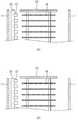
도 1은 본 발명의 일실시예에 따른 화학 기상 증착 장치를 개략적으로 나타내는 단면도이다.
도 2는 도 1의 화학 기상 증착 장치를 개략적으로 나타내는 평면도이다.
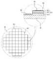
도 3은 도 1에서 가스 공급부를 개략적으로 나타내는 도면이다.
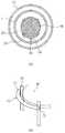
도 4는 적재된 각 웨이퍼에 대해 가스 공급부의 분사노즐이 배치되는 위치를 나타내는 단면도이다.
도 5는 가스 공급부를 통해 각 웨이퍼의 표면에 박막이 증착되는 원리를 개략적으로 나타내는 단면도이다.
도 6은 도 5에서 웨이퍼의 상면 또는 상면과 하면에 각각 박막이 성장된 상태를 개략적으로 나타내는 단면도이다.
도 7은 도 6의 에피 박막이 이루는 발광구조물의 구조를 보다 상세히 나타내는 도면이다.
도 8은 도 1의 가스 공급부의 변형예를 개략적으로 나타내는 도면이다.
도 9 및 도 10은 도 1의 가스 공급부의 다른 변형예를 개략적으로 나타내는 도면이다.
도 11 내지 도 13은 도 1의 가스 공급부의 또 다른 변형예를 개략적으로 나타내는 도면이다.
도 14는 본 발명의 다른 실시형태에 따른 화학 기상 증착 장치를 개략적으로 나타내는 도면이다.
도 15는 도 14에서 가이드부를 개략적으로 나타내는 도면이다.
도 16은 도 14의 단면도이다.
도 17 및 도 18은 도 14의 다른 실시형태에 따른 화학 기상 증착 장치를 개략적으로 나타내는 도면이다.1 is a cross-sectional view schematically showing a chemical vapor deposition apparatus according to an embodiment of the present invention.
FIG. 2 is a plan view schematically illustrating the chemical vapor deposition apparatus of FIG. 1.
3 is a view schematically illustrating a gas supply unit in FIG. 1.
4 is a cross-sectional view showing a position where the injection nozzles of the gas supply unit are disposed for each wafer loaded.
5 is a cross-sectional view schematically illustrating a principle in which a thin film is deposited on a surface of each wafer through a gas supply unit.
FIG. 6 is a cross-sectional view schematically illustrating a state in which a thin film is grown on an upper surface or an upper surface and a lower surface of a wafer in FIG. 5.
7 is a view illustrating in more detail the structure of the light emitting structure of the epi thin film of FIG.
8 is a view schematically showing a modification of the gas supply part of FIG. 1.
9 and 10 are diagrams schematically showing another modified example of the gas supply part of FIG. 1.
11 to 13 are diagrams schematically showing still another modified example of the gas supply part of FIG. 1.
14 is a diagram schematically showing a chemical vapor deposition apparatus according to another embodiment of the present invention.
FIG. 15 is a view schematically illustrating a guide unit in FIG. 14.
16 is a cross-sectional view of FIG. 14.
17 and 18 are diagrams schematically showing a chemical vapor deposition apparatus according to another embodiment of FIG. 14.
본 발명의 실시예에 따른 화학 기상 증착 장치 및 이를 이용한 반도체 에피 박막의 제조 방법에 관한 사항을 도면을 참조하여 설명한다.With reference to the drawings will be described with respect to the chemical vapor deposition apparatus according to an embodiment of the present invention and a method for manufacturing a semiconductor epi thin film using the same.
그러나, 본 발명의 실시예는 여러가지 다른 형태로 변형될 수 있으며, 본 발명의 범위가 이하 설명되는 실시예로 한정되는 것은 아니다. 본 발명의 실시예는 본 발명이 속하는 기술분야에서 통상의 지식을 가진 자에게 본 발명을 보다 완전하게 설명하기 위하여 제공되는 것이다.However, embodiments of the present invention may be modified in many different forms and the scope of the present invention is not limited to the embodiments described below. The embodiments of the present invention are provided to more completely explain the present invention to those skilled in the art.
따라서, 도면에 도시된 구성요소들의 형상 및 크기 등은 보다 명확한 설명을 위하여 과장될 수 있으며, 도면 상에서 실질적으로 동일한 구성과 기능을 가진 구성요소들은 동일한 참조부호를 사용할 것이다.Therefore, the shape and size of the components shown in the drawings may be exaggerated for more clear description, components having substantially the same configuration and function in the drawings will use the same reference numerals.
도 1 내지 도 5를 참조하여 본 발명의 일 실시형태에 따른 화학 기상 증착 장치를 설명한다.A chemical vapor deposition apparatus according to an embodiment of the present invention will be described with reference to FIGS. 1 to 5.
도 1은 본 발명의 일실시예에 따른 화학 기상 증착 장치를 개략적으로 나타내는 단면도이고, 도 2는 도 1의 화학 기상 증착 장치를 개략적으로 나타내는 평면도이며, 도 3은 도 1에서 가스 공급부를 개략적으로 나타내는 도면이다. 도 4는 적재된 각 웨이퍼에 대해 가스 공급부의 분사노즐이 배치되는 위치를 나타내는 단면도이고, 도 5는 가스 공급부를 통해 각 웨이퍼의 표면에 박막이 증착되는 원리를 개략적으로 나타내는 단면도이다.1 is a cross-sectional view schematically showing a chemical vapor deposition apparatus according to an embodiment of the present invention, FIG. 2 is a plan view schematically showing the chemical vapor deposition apparatus of FIG. 1, FIG. 3 is a schematic diagram of a gas supply unit in FIG. It is a figure which shows. 4 is a cross-sectional view showing a position where the injection nozzle of the gas supply unit is disposed for each wafer loaded, and FIG. 5 is a cross-sectional view schematically illustrating the principle that a thin film is deposited on the surface of each wafer through the gas supply unit.
도 1 내지 도 3을 참조하면, 본 발명의 실시예에 따른 화학 기상 증착 장치(1)는 반응 챔버(10), 웨이퍼 홀더(20), 가스 공급부(30)를 포함하고, 상기 웨이퍼 홀더(20)와 연결되어 상기 웨이퍼 홀더(20)를 회전시키는 회전 구동부(50)를 더 포함할 수 있다. 그리고, 상기 반응 챔버(10)의 둘레를 따라 구비되어 상기 반응 챔버(10) 내부를 가열하는 가열 수단(60)을 더 포함할 수 있다. 이를 통해 상기 반응 챔버(10)는 높은 온도 균일성을 유지할 수 있다.
1 to 3, a chemical
상기 반응 챔버(10)는 소정 크기의 내부공간을 가지며 상부 및 하부가 개방된 원통형 구조의 내부관(11) 및 상기 내부관(11)을 덮어 기밀을 유지하도록 하부가 개방된 외부관(12)의 2중 구조로 구성된다. 그리고, 상기 내부관(11)의 하부에는 베이스 플레이트(13)가 개폐가능하도록 구비된다. 상기 내부관(11)과 외부관(12) 그리고 베이스 플레이트(13)는 석영(quartz) 또는 탄화규소(SiC)로 이루어질 수 있다.
The
상기 웨이퍼 홀더(20)에는 박막 성장을 위한 복수개의 웨이퍼(w)가 소정 간격으로 적재되어 구비되며, 웨이퍼(w)가 적재된 상기 웨이퍼 홀더(20)는 상기 베이스 플레이트(13)의 개폐를 통해 상기 내부관(11) 내에 배치되거나 외부로 배출될 수 있다. 상기 웨이퍼 홀더(20)는 고온 및 고압 분위기의 반응 챔버(10) 내에서 열변형되지 않도록 석영 등의 재질로 이루어질 수 있으나 이에 한정하는 것은 아니다.The
이와 같이, 웨이퍼 홀더(20)를 통해 수백매의 웨이퍼(w)를 소정 간격으로 적재함으로써 종래와 같이 서섭테 상에 웨이퍼(w)를 수매만 장착하여 성장시키는 것에 비해 대량생산이 가능하다는 장점을 갖는다.Thus, by loading hundreds of wafers (w) at predetermined intervals through the
상기 웨이퍼 홀더(20)는 단열판에 의해 보호되는 회전 구동부(50)와 연결되어 상기 회전 구동부(50)에서 가해지는 회전력에 의해 상기 내부관(11) 내에서 소정 속도로 회전할 수 있다. 따라서, 에피 박막(80)이 웨이퍼(w)의 표면 전체에 걸쳐 보다 균일하게 성장할 수 있도록 한다.
The
상기 가스 공급부(30)는 상기 웨이퍼의 표면에 반도체 에피 박막을 성장시키도록 상기 반응 챔버(10) 내부로 외부로부터 반응가스(G)를 공급하는 적어도 하나의 가스 라인(31) 및 상기 가스 라인(31)과 연통하여 상기 반응가스(G)를 상기 웨이퍼(w)로 분사하는 복수개의 분사노즐(33)을 포함한다. 그리고, 상기 반응가스(G)를 냉각시키도록 상기 가스 라인(31)의 둘레를 따라 구비되는 냉각 라인(32)을 더 포함할 수 있다.The
구체적으로, 상기 가스 라인(31)과 냉각 라인(32)을 포함한 상기 가스 공급부(30)는 상기 내부관(11)과 웨이퍼 홀더(20) 사이에서 상기 웨이퍼(w)의 적재방향을 따라 수직하게 연장되어 구비된다. 그리고, 상기 냉각 라인(32)의 내부에는 가스 라인(31)이 배치되는 2중 구조를 갖는다. 즉, 반응가스(G)가 흐르는 가스 라인(31)을 냉매(C)가 흐르는 냉각 라인(32)이 감싸서 냉각시킴으로써 상기 반응가스(G)가 고온분위기 하에서 가스 라인(31)을 따라 반응 챔버(10) 내부로 공급되는 도중에 반응을 일으켜 가스 라인(31) 내부에서 증착되는 것을 방지한다.Specifically, the
상기 반응가스(G)는 질화물 반도체(Ga(Al, In)N)의 합금 형태 및 도핑 소스로 사용되는 것으로 TMGa, TEGa, TMIn, TMAl, SiH4, Cp2Mg, DEZn, NH3, H2, N2 등을 포함할 수 있다. 그리고, 산화물 반도체(Zn(Cd, Mg)O)의 합금 형태 및 도핑 소스로 사용되는 것으로 DEZn, TMGa, TEGa, TMIn, TMAl, Cd[(EPiPr2)2N]2 (E=S, Se), TMSb, Cp2Mg, N2, Ar, O2, N2O, O3 등을 포함할 수 있다.The reaction gas (G) is used as an alloy and a doping source of nitride semiconductors (Ga (Al, In) N), TMGa, TEGa, TMIn, TMAl, SiH4 , Cp2 Mg, DEZn, NH3 , H2 , N2 , and the like. In addition, it is used as an alloy form and doping source of oxide semiconductors (Zn (Cd, Mg) O), DEZn, TMGa, TEGa, TMIn, TMAl, Cd [(EPiPr2 )2 N]2 (E = S, Se) , TMSb, Cp2 Mg, N2 , Ar, O2 , N2 O, O3 , and the like.
상기 분사노즐(33)은 복수개가 상기 가스 공급부(30), 구체적으로는 상기 냉각 라인(32)의 길이방향을 따라 상기 냉각 라인(32)의 표면으로부터 돌출되어 각 웨이퍼(w)의 위치와 대응하는 위치에 구비되며, 각각 상기 가스 라인(31)과 연통된다.The plurality of
도 4a에서와 같이, 상기 복수개의 분사노즐(33)은 상기 적재된 웨이퍼(w)의 각 측면과 마주하도록 상기 웨이퍼(w)의 적재간격에 대응하여 배열될 수 있다. 또한, 도 4b에서와 같이, 상기 복수개의 분사노즐(33)은 상기 적재된 웨이퍼(w)와 웨이퍼(w) 사이에 위치하도록 배열될 수도 있다. 이러한 구조를 통해 상기 분사노즐(33)은 각각 상기 웨이퍼(w)의 표면으로 반응가스(G)를 분사하여 각 웨이퍼(w)의 표면에 에피 박막(80)을 형성한다.As shown in FIG. 4A, the plurality of
구체적으로, 도 5a 및 5b에서 처럼, 상기 분사노즐(33)은 각 웨이퍼(w)의 일면, 즉 상면으로 반응가스(G)를 분사하여 웨이퍼(w)의 상면에만 에피 박막(80)을 형성할 수 있다. 또한, 도 5c 및 5d에서 처럼, 각 웨이퍼(w)의 상면과 하면으로 반응가스(G)를 분사하여 각 웨이퍼(w)의 상면과 하면에 에피 박막(80)을 동시에 형성할 수도 있다. 즉, 복수개의 분사노즐(33) 각각은 적재된 각각의 웨이퍼(w)와 대응하여 배치되어 각 웨이퍼(w)의 상면과 하면으로 반응가스(G)가 흐르도록 분사함으로써 각 웨이퍼(w)의 상면과 하면의 양면에 각각 에피 박막(80)이 성장할 수 있도록 한다.Specifically, as shown in FIGS. 5A and 5B, the
이와 같이, 웨이퍼(w)의 상면과 하면의 양면에 각각 에피 박막(80)이 형성되는 경우 단일의 웨이퍼(w)로부터 두개의 에피 박막으로 이루어지는 발광구조물(80')을 얻을 수 있어 생산성이 향상되는 대량생산에 유리한 장점이 있다.Thus, when the epi
또한, 이러한 웨이퍼(w) 양면에서의 에피 박막(80)의 성장은 응력(f)에 의한 웨이퍼(w)의 변형을 방지할 수 있다. 즉, 종래의 화학 기상 증착 장치에서와 같이 웨이퍼(w)의 일면에만 에피 박막(80)이 성장하는 경우, 에피 박막에 강한 응력(f)이 작용하여 오목한 형상을 이루도록 휨 현상(bowing effect)이 발생하며, 이러한 현상은 대구경화가 될수록 심해져 웨이퍼가 파손되거나 성능 열화와 같은 문제점이 발생할 수 있다. 그러나, 본 실시예에서와 같이 웨이퍼(w)의 양면에 에피 박막(80)을 성장시키는 경우 웨이퍼(w)의 상면과 하면에서 발생되는 응력(f)이 서로 완화됨으로써 종래의 문제점들을 해결할 수 있다. 특히, 웨이퍼(w)의 대구경화가 가능하여 생산성이 향상되는 장점을 갖는다.
In addition, growth of the epi
도 6은 도 5에서 웨이퍼의 상면 또는 상면과 하면에 각각 박막이 성장된 상태를 개략적으로 나타내는 단면도이고, 도 7은 도 6의 에피 박막이 이루는 발광구조물의 구조를 보다 상세히 나타내는 도면이다.FIG. 6 is a cross-sectional view schematically illustrating a state in which a thin film is grown on a top surface or a top surface and a bottom surface of a wafer in FIG. 5, and FIG. 7 is a view illustrating the light emitting structure of the epi thin film of FIG. 6 in more detail.
도 6 및 도 7에서와 같이, 상기 웨이퍼(w)의 표면에 성장되는 상기 에피 박막(80)은 제1 도전형 반도체층(81), 활성층(82), 제2 도전형 반도체층(83)의 순서로 형성되는 발광구조물(80')을 포함한다. 그리고, 상기 발광구조물(80')은 상기 제1 도전형 반도체층(81)과 제2 도전형 반도체층(83) 상에 각각 형성되는 제1 전극(84) 및 제2 전극(85)을 더 포함할 수 있다.As shown in FIGS. 6 and 7, the epi
상기 제1 및 제2 도전형 반도체층(81,83)은 각각 n형 및 p형 반도체층이 될 수 있으며, 질화물 반도체로 이루어질 수 있다. 따라서, 이에 제한되는 것은 아니지만, 본 실시예의 경우, 제1 및 제2 도전형은 각각 n형 및 p형을 의미하는 것으로 이해될 수 있다.The first and second conductive semiconductor layers 81 and 83 may be n-type and p-type semiconductor layers, respectively, and may be formed of a nitride semiconductor. Therefore, the present invention is not limited thereto, but in the present embodiment, the first and second conductivity types may be understood to mean n-type and p-type, respectively.
상기 제1 도전형 반도체층(81)은 AlxInyGa(1-x-y)N 조성식(여기서, 0≤x≤1, 0≤y≤1, 0≤x+y≤1임)을 갖는 n형 불순물이 도핑된 반도체 물질로 이루어질 수 있으며, 대표적으로 GaN, AlGaN, InGaN이 있다. 그리고, 제1 도전형 반도체층(81)의 도핑에 사용되는 불순물로는 Si, Ge, Se, Te 또는 C 등이 사용될 수 있다.The first
제1 도전형 반도체층(81)상에 형성되는 활성층(82)은 전자와 정공이 재결합하여 빛을 발광하기 위한 층으로서, 통상 InGaN층을 양자우물층으로 하고, (Al)GaN층을 양자장벽층(barrier layer)으로 하여 서로 교대로 배치시켜 형성된 다중양자우물구조(MQW)를 가진다. 청색 발광다이오드에서는 InGaN/GaN 등의 다중양자우물구조, 자외선 발광다이오드에서는 GaN/AlGaN, InAlGaN/InAlGaN 및 InGaN/AlGaN 등의 다중양자우물구조가 사용되고 있다. 이러한 활성층(82)의 효율 향상에 대해서는, In 또는 Al의 조성비율을 변화시킴으로써 빛의 파장을 조절하거나, 활성층(82) 내의 양자우물층의 깊이, 활성층의 수, 두께 등을 변화시킴으로써 발광구조물의 내부 양자 효율을 향상시키고 있다.The
제2 도전형 반도체층(83)은 제1 도전형 반도체층(81)과 마찬가지로, AlxInyGa(1-x-y)N 조성식(여기서, 0≤x≤1, 0≤y≤1, 0≤x+y≤1임)을 갖는 p형 불순물이 도핑된 반도체 물질로 이루어질 수 있으며, 대표적으로는 GaN, AlGaN, InGaN이 있다. 이러한 제2 도전형 반도체층(83)의 도핑에 사용되는 불순물로는 Mg, Zn 또는 Be 등이 있다.Similar to the first
상기 제1 도전형 반도체층(81)과 제2 도전형 반도체층(83) 상에는 전류의 공급을 위한 제1 전극(84)과 제2 전극(85)이 각각 형성되어 상기 제1 및 제2 도전형 반도체층(81,83)과 각각 전기적으로 연결된다. 이에 따라 제1 전극(84)과 제2 전극(85)을 통해 전류를 공급함으로써 빛을 방출할 수 있다. 구체적으로, 상기 제1 전극(84)은 메사 식각되어 일부가 노출되는 상기 제1 도전형 반도체층(81) 상에 형성되고, 상기 제2 전극(85)은 상기 제2 도전형 반도체층(83) 상에 형성되는 투명전극층(86) 상에 형성될 수 있다.The
상기 제1 전극(84)은 상기 제1 도전형 반도체층(81) 상에 Ti, Cr, Al, Cu 및 Au로 구성된 그룹으로부터 선택된 물질로 이루어진 단일층 또는 복수층으로 형성될 수 있다.The
상기 제2 전극(85)은 향후 발광구조물을 패키징 하여 발광소자 패키지를 제작시 와이어 본딩을 통해 리드 상에 탑재될 최외곽 전극층으로서, 일반적으로 Au 또는 Au를 함유한 합금을 재료로 하여 형성될 수 있다.The
상기 투명전극층(86)은 제2 도전형 반도체층(83)의 상면의 거의 전 영역에 형성되는 것이 바람직하며, 비교적 높은 에너지밴드갭을 갖는 제2 도전형 반도체층(83)과의 접촉저항을 낮추는데 적절하면서 동시에 상기 활성층(82)에서 생성되는 빛이 상부로 방출되기 위해 양호한 투광성을 갖는 물질로 형성될 것이 요구된다.The
일반적으로 상기 투명전극층(86)은 접촉저항은 비교적 높으나 양호한 투광성을 확보하기 위해 인듐-주석계 산화물(ITO), 인듐 산화물(IO), 주석계 산화물(SnO2), 아연계 산화물(ZnO) 및 인듐-아연계 산화물(IZO)로 구성된 그룹으로부터 선택된 산화물로 이루어진 적어도 한 개의 층으로 형성되는 것이 바람직하다. 상기 투명전극층(86)은 동작 전압의 감소 및 빛의 외부 방출 효율을 향상시킬 수 있다.In general, the
본 실시예에서는 상기 발광구조물을 이루는 제1 및 제2 도전형 반도체층(81,83)이 질화물 반도체로 이루어지는 것으로 설명하고 있으나 이에 한정하는 것은 아니며, 산화물 반도체로 이루어지는 것도 가능하다.
In the present exemplary embodiment, the first and second conductive semiconductor layers 81 and 83 constituting the light emitting structure are described as being made of nitride semiconductor, but the present invention is not limited thereto.
도 8 내지 도 13을 참조하여 상기 가스 공급부의 다른 변형예를 설명한다.Another modified example of the gas supply unit will be described with reference to FIGS. 8 to 13.
도 8은 도 1의 가스 공급부의 변형예를 개략적으로 나타내는 도면이고, 도 9 및 도 10은 도 1의 가스 공급부의 다른 변형예를 개략적으로 나타내는 도면이며, 도 11 내지 도 13은 도 1의 가스 공급부의 또 다른 변형예를 개략적으로 나타내는 도면이다.FIG. 8 is a view schematically showing a modification of the gas supply unit of FIG. 1, and FIGS. 9 and 10 are views schematically showing another modification of the gas supply unit of FIG. 1, and FIGS. 11 to 13 are gas of FIG. 1. It is a figure which shows schematically another modified example of a supply part.
도 8에서와 같이 상기 가스 공급부(30')는 제1 반응가스(G1)를 공급하는 제1 가스 라인(31-1) 및 제2 반응가스(G2)를 공급하는 제2 가스 라인(31-2)을 포함하며, 상기 제1 및 제2 가스 라인(31-1,31-2)은 상기 냉각 라인(32) 내부에 배치될 수 있다. 구체적으로, 도 3에서와 같이 단일의 가스 라인(31)이 구비되는 것과 달리 2개 이상의 가스 라인(31-1,31-2)이 냉각 라인(32) 내부에 구비되어 제1 반응가스(G1)와 제2 반응가스(G2)를 구분하여 공급할 수 있는 것이다. 도면에서는 2개의 가스 라인(31-1,31-2)이 구비되는 것으로 도시하고 있으나 이에 한정하지 않고 반응가스의 종류에 따라서 가스 라인의 수는 증가될 수 있다.As shown in FIG. 8, the
도 9 및 도 10은 도 1의 가스 공급부의 다른 변형예를 개략적으로 나타내는 도면이다.9 and 10 are diagrams schematically showing another modified example of the gas supply part of FIG. 1.
도 9 및 도 10에서와 같이, 상기 가스 공급부(30)는 하나 이상 구비되어 동일한 반응가스를 공급하거나 또는 각각 상이한 반응가스를 구분하여 공급할 수 있다. 즉, 도 2에서와 같이 단일의 가스 공급부(30)가 구비되는 것과 달리 2개 이상의 가스 공급부(30)가 내부관(11)과 웨이퍼 홀더(20) 사이에서 웨이퍼(w)의 적재방향을 따라 수직하게 연장되어 구비될 수 있다. 이 경우, 각 가스 공급부(30)는 서로 상이한 반응가스를 구분하여 공급할 수 있다. 그리고, 각 가스 공급부(30)는 도 3에서와 같이 단일의 가스 라인(31)을 구비하거나, 도 8에서와 같이 복수의 가스 라인(31-1,31-2)을 구비할 수 있다.9 and 10, the
도 11 내지 도 13은 도 1의 가스 공급부의 또 다른 변형예를 개략적으로 나타내는 도면이다.11 to 13 are diagrams schematically showing still another modified example of the gas supply part of FIG. 1.
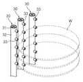
도 11 내지 도 13에서와 같이, 상기 가스 공급부(30'')는 상기 가스 라인(31) 및 상기 냉각 라인(32)과 연통하며, 상기 웨이퍼(w)를 에워싸도록 각각의 웨이퍼(w) 둘레를 따라 웨이퍼와 수평하게 구비되어 반응가스(G)를 분사하는 보조 라인(34)을 더 포함할 수 있다. 구체적으로, 상기 보조 라인(34)은 내부관(11)과 웨이퍼 홀더(20) 사이에서 웨이퍼(w)의 적층방향을 따라 수직하게 연장되는 가스 공급부(30'')로부터 각 웨이퍼(w)의 둘레를 감싸도록 수직하게 연장되어 구비된다.11 to 13, the
상기 보조 라인(34)은 상기 웨이퍼(w) 보다 큰 지름의 환고리 형태를 갖는다. 그리고, 상기 가스 라인(31)과 연통하여 공급된 반응가스(G)를 분사하는 복수의 분사노즐(33)을 구비하는 보조 가스 라인(35) 및 상기 냉각 라인(32)과 연통하여 상기 반응가스(G)를 냉각시키도록 상기 보조 가스 라인(35)의 둘레를 따라 구비되어 냉매(C)가 흐르는 보조 냉각 라인(36)을 포함할 수 있다.The
또한, 도 13에서 처럼 상기 보조 라인(34)은 제1 반응가스(G1)를 공급하는 제1 보조 가스 라인(35-1) 및 제2 반응가스(G2)를 공급하는 제2 보조 가스 라인(35-2)을 포함하여 상기 제1 반응가스(G1)와 제2 반응가스(G2)를 구분하여 공급하도록 할 수 있다.In addition, as shown in FIG. 13, the
상기 보조 라인(34)은 상기 적재된 웨이퍼(w)와 다른 웨이퍼 사이에 위치하거나, 상기 각 웨이퍼(w)의 각 측면과 마주하도록 상기 웨이퍼(w)의 적재간격에 대응하여 배열될 수 있다.
The
한편, 도 14 내지 도 18을 참조하여 본 발명의 다른 실시형태에 따른 화학 기상 증착 장치를 설명한다.Meanwhile, a chemical vapor deposition apparatus according to another embodiment of the present invention will be described with reference to FIGS. 14 to 18.
도 14는 본 발명의 다른 실시형태에 따른 화학 기상 증착 장치를 개략적으로 나타내는 도면이고, 도 15는 도 14에서 가이드부를 개략적으로 나타내는 도면이며, 도 16은 도 14의 단면도이고, 도 17 및 도 18은 도 14의 다른 실시형태에 따른 화학 기상 증착 장치를 개략적으로 나타내는 도면이다.14 is a view schematically showing a chemical vapor deposition apparatus according to another embodiment of the present invention, FIG. 15 is a view schematically showing a guide part in FIG. 14, FIG. 16 is a cross-sectional view of FIG. 14, and FIGS. 17 and 18. 14 is a diagram schematically illustrating a chemical vapor deposition apparatus according to another embodiment of FIG. 14.
도 14의 실시형태에 따른 화학 기상 증착 장치의 경우, 도 1의 실시형태와 기본적인 구조는 실질적으로 동일하다. 다만, 분사노즐에서 분사되는 반응가스의 흐름을 안내하는 가이드부(70)를 더 구비하는 점에서 차이가 있다. 따라서, 이하에서는 도 1의 실시형태와 중복되는 부분에 관한 설명은 생략하고 가이드부(70)에 관한 구성을 위주로 설명한다.In the case of the chemical vapor deposition apparatus according to the embodiment of FIG. 14, the basic structure of the embodiment of FIG. 1 is substantially the same. However, there is a difference in that it further comprises a
도 14에 도시된 바와 같이, 상기 가이드부(70)는 상기 분사노즐(33)에서 분사되는 상기 반응가스(G)가 상기 각 웨이퍼(w)의 상면과 하면으로 분사되어 흐르도록 상기 반응가스(G)의 흐름을 안내한다. 구체적으로, 상기 가이드부(70)는 상기 분사노즐(33)과 웨이퍼(w) 사이에 배치되며, 상기 웨이퍼(w)로부터 상기 분사노즐(33)을 향해 단면적이 감소하도록 상기 분사노즐(33)을 향해 각각 기울어져 서로 접하는 상부 경사면(71) 및 하부 경사면(72)을 포함한다. 따라서, 도면에서와 같이 단면이 삼각형 형태의 구조를 가지며, 상부 경사면(71)과 하부 경사면(72)이 만나는 꼭지점이 상기 분사노즐(33)을 향하는 구조로 구비된다.As illustrated in FIG. 14, the
도 14에서와 같이, 상기 가이드부(70)는 복수개가 상기 웨이퍼 홀더(20)로부터 상기 분사노즐(33)을 향해 연장되어 상기 웨이퍼(w)의 적재방향을 따라 수직하게 배열되어 구비될 수 있다. 구체적으로, 상기 가스 공급부(30)와 마주하는 상기 웨이퍼 홀더(20)의 외측면과 접하여 일체로 구비될 수 있다.As shown in FIG. 14, a plurality of
그리고, 도 15에서와 같이 상기 가이드부(70)는 적어도 한 쌍의 지지핀(p)에 의해 상기 웨이퍼(w)의 적재방향을 따라 수직하게 배열되어 구비되며, 상기 분사노즐(33)과 마주하도록 상기 웨이퍼 홀더(20)에 분리가능하게 장착될 수도 있다.In addition, as shown in FIG. 15, the
상기 가이드부(70)는 반응가스(G)를 분사하는 상기 분사노즐(33)의 배치구조와 대응하여 배치된다. 즉, 도 16a에서 처럼 상기 복수개의 분사노즐(33)이 상기 적재된 웨이퍼(w)의 측면과 마주하는 구조로 배열되는 경우 상기 가이드부(40)는 전면인 꼭지점이 상기 분사노즐(33)과 마주하고, 후면은 상기 적재된 웨이퍼(w)의 각 측면과 마주하도록 상기 웨이퍼(w)의 적재간격에 대응하여 수직하게 배열되어 구비될 수 있다.The
또한, 도 16b에서 처럼 상기 복수개의 분사노즐(33)이 상기 적재된 웨이퍼(w)와 웨이퍼(w) 사이에 위치하도록 배열되는 경우 상기 가이드부(70)도 상기 적재된 웨이퍼(w)와 웨이퍼(w) 사이의 공간과 마주하도록 상기 웨이퍼(w)의 적재간격에 대응하여 수직하게 배열되어 구비될 수 있다. 따라서, 상기 분사노즐(33)에서 분사되는 반응가스(G)가 각 웨이퍼(w)의 상면과 하면으로 흐르도록 방향을 안내하고, 이를 통해 각 웨이퍼(w)의 상면과 하면의 양면에는 에피 박막(80)이 성장될 수 있는 것이다.In addition, as shown in FIG. 16B, when the plurality of
상기 가스 공급부(30'')가 보조 라인(34)을 구비하는 경우, 상기 가이드부(70)는 도 18에서 처럼 상기 보조 라인(34)과 상기 웨이퍼 홀더(20) 사이에서 환고리 형태로 상기 웨이퍼(w)의 둘레를 따라서 구비될 수 있다. 즉, 상기 웨이퍼(w) 보다 크고 상기 보조 라인(34)보다 작은 지름의 환고리 형태를 가질 수 있다.
When the
한편, 이하에서는 본 발명의 일실시예에 따른 화학 기상 증착 장치를 이용한 반도체 에피 박막의 제조 방법에 대해 설명한다. 하기의 설명은 도 1 내지 도 18에 도시된 화학 기상 증착 장치를 참조한다.Meanwhile, a method of manufacturing a semiconductor epitaxial thin film using a chemical vapor deposition apparatus according to an embodiment of the present invention will be described below. The following description refers to the chemical vapor deposition apparatus shown in FIGS. 1 to 18.
우선, 웨이퍼 홀더(20)에 복수의 웨이퍼(w)를 소정 간격으로 적재하여 장착하고, 상기 웨이퍼 홀더(20)를 가스 공급부(30)가 구비된 반응 챔버(10)의 내부관(11) 내에 배치한다. 상기 웨이퍼 홀더(20)는 상기 내부관(11)의 하부에 개폐가능하도록 구비되는 베이스 플레이트(13)를 통해 상기 내부관(11) 내에 배치되거나 배출될 수 있다.First, a plurality of wafers w are mounted on the
이 경우, 상기 가스 공급부(30)와 상기 웨이퍼 홀더(20) 사이에는 상기 가스 공급부에서 분사되는 반응가스의 흐름을 안내하도록 가이드부(70)를 더 구비할 수 있다.In this case, a
상기 가이드부(70)는 상기 웨이퍼(w)로부터 상기 가스 공급부(30)를 향해 단면적이 감소하도록 상기 가스 공급부(30)를 향해 각각 기울어져 서로 접하는 상부 경사면(71) 및 하부 경사면(72)을 포함할 수 있다. 그리고, 상기 가이드부(70)는 상기 적재된 웨이퍼(w)의 각 측면과 마주하거나, 상기 적재된 웨이퍼(w)와 웨이퍼(w) 사이의 공간과 마주하도록 상기 웨이퍼(w)의 적재간격에 대응하여 수직하게 배열되어 구비될 수 있다. 상기 가이드부(70)의 구체적인 배치구조에 대해서는 이미 전술한 화학 기상 증착 장치(1)에서 상세히 설명하였으므로 본 실시예에서는 이에 대한 설명을 생략한다.The
다음으로, 상기 내부관(11)과 웨이퍼 홀더(20) 사이에서 상기 웨이퍼(w)의 적재방향을 따라 수직하게 연장되어 구비되는 상기 가스 공급부(30)를 통해 외부의 반응가스(G)를 상기 웨이퍼(w)로 분사한다.Next, the external reaction gas (G) through the
상기 가스 공급부(30)는 상기 반응 챔버(10) 내부로 상기 반응가스(G)를 공급하는 적어도 하나의 가스 라인(31) 및 상기 가스 라인(31)과 연통하여 상기 반응가스(G)를 상기 웨이퍼(w) 각각에 대해 분사하는 복수개의 분사노즐(33)을 갖는다. 그리고, 상기 가스 공급부(30)는 상기 반응가스(G)를 냉각시키도록 상기 가스 라인(31)의 둘레를 따라 구비되어 냉매(C)가 흐르는 냉각 라인(32)을 더 포함할 수 있다. 여기서, 상기 복수개의 분사노즐(33)은 상기 적재된 웨이퍼(w)의 각 측면과 마주하거나, 상기 적재된 웨이퍼(w)와 웨이퍼(w) 사이에 위치하도록 상기 웨이퍼(w)의 적재간격에 대응하여 배열될 수 있다. 상기 가스 공급부(30)는 하나 또는 하나 이상 구비되어 각각 동일한 반응가스(G)를 공급하거나 또는 상이한 반응가스(G)를 구분하여 공급할 수 있다.The
다음으로, 상기 가스 공급부(30)에서 분사되는 상기 반응가스(G)가 각 웨이퍼(w)의 표면, 구체적으로 각 웨이퍼(w)의 상면 또는 상면과 하면을 따라 흐르도록 하여 각 웨이퍼(w)의 표면에 반도체 에피 박막(80)을 성장시킨다. 여기서, 각 웨이퍼(w)의 표면에 성장되는 상기 반도체 에피 박막(80)은 제1 도전형 반도체층(81), 활성층(82), 제2 도전형 반도체층(83)의 순서로 성장되어 발광구조물(80')을 형성한다. 그리고, 상기 제1 도전형 반도체층(81)과 제2 도전형 반도체층(83) 상에는 각각 제1 전극(84) 및 제2 전극(85)을 형성하여 상기 제1 도전형 반도체층(81) 및 제2 도전형 반도체층(83)과 전기적으로 연결되도록 한다. 이러한 발광구조물은 향후 다이싱 공정을 거쳐 개별 소자로 싱귤레이팅되어 복수의 발광소자 칩으로 제조된다.Next, the reaction gas G injected from the
이와 같이, 본 발명에 따른 화학 기상 증착 장치(1)는 웨이퍼 홀더(20)를 통해 적재되는 수백매의 웨이퍼 각각에 대응하여 분사노즐(33)을 구비하여 반응가스(G)를 분사함으로써 각 웨이퍼(w)의 표면에 반도체 에피 박막(80)이 성장될 수 있도록 한다.As such, the chemical
또한, 각 분사노즐(33)과 마주하는 가이드부(70)를 더 구비함으로써 분사노즐(33)에서 분사되는 반응가스(G)가 각 웨이퍼(w)의 상면과 하면으로 흐르도록 안내하여 웨이퍼(w)의 상면과 하면에 에피 박막(80)이 성장할 수 있도록 한다.In addition, by further providing a
따라서, 대량생산이 가능하여 생산성이 향상되고, 특히 대구경 웨이퍼를 사용하더라도 에피 박막이 양면에서 성장하여 응력을 완화시켜줌으로써 휨 변형이 발생하지 않아 품질이 우수하다.
Therefore, mass production is possible and productivity is improved. Especially, even when using a large-diameter wafer, the epi thin film grows on both sides to relieve stress, so that bending deformation does not occur and thus quality is excellent.
10....... 반응 챔버11....... 내부관
12....... 외부관20....... 웨이퍼 홀더
30....... 가스 공급부31....... 가스 라인
32....... 냉각 라인33....... 분사노즐
50....... 회전 구동부60....... 가열 수단
80....... 에피 박막10 .......
12 .......
30 .......
32 ....... Cooling
50 ....... Rotary drive 60 ....... Heating means
80 ....... Epi thin film
Claims (27)
Translated fromKorean상기 내부관 내에 배치되며, 복수개의 웨이퍼가 소정 간격으로 적재되어 구비되는 웨이퍼 홀더;
상기 웨이퍼의 표면에 반도체 에피 박막을 성장시키도록 상기 반응 챔버 내부로 외부로부터 반응가스를 공급하는 적어도 하나의 가스 라인 및 상기 가스 라인과 연통하여 상기 반응가스를 상기 웨이퍼 각각에 대해 분사하는 복수개의 분사노즐을 갖는 가스 공급부; 및
상기 분사노즐에서 분사되는 상기 반응가스가 상기 각 웨이퍼의 상면과 하면으로 분사되어 흐르도록 상기 반응가스의 흐름을 안내하는 가이드부;를 포함하고,
상기 웨이퍼의 표면에 성장되는 상기 반도체 에피 박막은 제1 도전형 반도체층, 활성층, 제2 도전형 반도체층의 순서로 형성된 발광구조물을 포함하는 것을 특징으로 하는 화학 기상 증착 장치.
A reaction chamber having an inner tube having an inner space of a predetermined size and an upper tube covering the inner tube to maintain airtightness;
A wafer holder disposed in the inner tube and having a plurality of wafers loaded at predetermined intervals;
At least one gas line for supplying a reaction gas from the outside into the reaction chamber so as to grow a semiconductor epitaxial film on the surface of the wafer, and a plurality of jets for injecting the reaction gas to each of the wafers in communication with the gas line A gas supply having a nozzle; And
And a guide unit configured to guide the flow of the reaction gas so that the reaction gas injected from the injection nozzle flows to the upper and lower surfaces of the respective wafers.
The semiconductor epitaxial thin film grown on the surface of the wafer comprises a light emitting structure formed in the order of the first conductive semiconductor layer, the active layer, the second conductive semiconductor layer.
상기 가스 공급부는 상기 웨이퍼의 적재방향을 따라 수직하게 연장되며, 상기 복수개의 분사노즐은 상기 적재된 웨이퍼의 각 측면과 마주하도록 상기 웨이퍼의 적재간격에 대응하여 배열되는 것을 특징으로 하는 화학 기상 증착 장치.
The method of claim 1,
The gas supply unit extends vertically along the stacking direction of the wafer, and the plurality of injection nozzles are arranged in correspondence with the stacking interval of the wafer so as to face each side of the loaded wafer. .
상기 가스 공급부는 상기 웨이퍼의 적재방향을 따라 수직하게 연장되며, 상기 복수개의 분사노즐은 상기 적재된 웨이퍼와 웨이퍼 사이에 위치하도록 배열되는 것을 특징으로 하는 화학 기상 증착 장치.
The method of claim 1,
And the gas supply part extends vertically along the loading direction of the wafer, wherein the plurality of injection nozzles are arranged to be positioned between the loaded wafer and the wafer.
상기 가스 공급부는 상기 반응가스를 냉각시키도록 상기 가스 라인의 둘레를 따라 구비되어 냉매가 흐르는 냉각 라인을 더 포함하는 것을 특징으로 하는 화학 기상 증착 장치.
The method of claim 1,
The gas supply unit further comprises a cooling line provided along the circumference of the gas line to cool the reaction gas flows through the refrigerant.
상기 가스 공급부는 제1 반응가스를 공급하는 제1 가스 라인 및 제2 반응가스를 공급하는 제2 가스 라인을 포함하며, 상기 제1 및 제2 가스 라인은 상기 냉각 라인 내부에 배치되는 것을 특징으로 하는 화학 기상 증착 장치.
5. The method of claim 4,
The gas supply unit includes a first gas line for supplying a first reaction gas and a second gas line for supplying a second reaction gas, wherein the first and second gas lines are disposed in the cooling line. Chemical vapor deposition apparatus.
상기 가스 공급부는 하나 이상 구비되어 각각 동일한 반응가스를 공급하거나 또는 상이한 반응가스를 구분하여 공급하는 것을 특징으로 하는 화학 기상 증착 장치.
The method according to claim 1 or 4,
One or more gas supply units are provided to supply the same reaction gas or to supply different reaction gases, respectively.
상기 가스 공급부는 상기 가스 라인 및 상기 냉각 라인과 연통하며, 상기 웨이퍼를 에워싸도록 각각의 웨이퍼 둘레를 따라 웨이퍼와 수평하게 구비되어 반응가스를 분사하는 보조 라인을 더 포함하는 것을 특징으로 하는 화학 기상 증착 장치.
The method according to claim 1 or 4,
The gas supply unit communicates with the gas line and the cooling line, and further includes an auxiliary line disposed horizontally with the wafer along each wafer circumference to surround the wafer to inject a reaction gas. Deposition apparatus.
상기 보조 라인은 상기 웨이퍼 보다 큰 지름의 환고리 형태를 가지며, 상기 가스 라인과 연통하여 공급된 반응가스를 분사하는 복수의 분사노즐을 구비하는 보조 가스 라인 및 상기 냉각 라인과 연통하여 상기 반응가스를 냉각시키도록 상기 보조 가스 라인의 둘레를 따라 구비되어 냉매가 흐르는 보조 냉각 라인을 포함하는 것을 특징으로 하는 화학 기상 증착 장치.
The method of claim 7, wherein
The auxiliary line has an annular shape having a larger diameter than the wafer, and has an auxiliary gas line having a plurality of injection nozzles for injecting a reaction gas supplied in communication with the gas line, and the reaction gas in communication with the cooling line. And an auxiliary cooling line provided along the circumference of the auxiliary gas line to cool the liquid, and the refrigerant flowing therethrough.
상기 보조 가스 라인은 제1 반응가스를 공급하는 제1 보조 가스 라인 및 제2 반응가스를 공급하는 제2 보조 가스 라인을 포함하는 것을 특징으로 하는 화학 기상 증착 장치.
9. The method of claim 8,
The auxiliary gas line includes a first auxiliary gas line for supplying a first reaction gas and a second auxiliary gas line for supplying a second reaction gas.
상기 보조 라인은 상기 적재된 웨이퍼와 다른 웨이퍼 사이에 위치하거나, 상기 웨이퍼의 각 측면과 마주하도록 상기 웨이퍼의 적재간격에 대응하여 배열되는 것을 특징으로 하는 화학 기상 증착 장치.
The method of claim 7, wherein
And the auxiliary line is positioned between the loaded wafer and another wafer, or arranged in correspondence with the loading interval of the wafer so as to face each side of the wafer.
상기 가이드부는 상기 분사노즐과 웨이퍼 사이에 배치되며, 상기 웨이퍼로부터 상기 분사노즐을 향해 단면적이 감소하도록 상기 분사노즐을 향해 각각 기울어져 서로 접하는 상부 경사면 및 하부 경사면을 포함하는 것을 특징으로 하는 화학 기상 증착 장치.
The method of claim 1,
The guide portion is disposed between the injection nozzle and the wafer, and the chemical vapor deposition characterized in that it comprises an upper inclined surface and a lower inclined surface inclined toward each of the injection nozzle in contact with each other to reduce the cross-sectional area from the wafer toward the injection nozzle Device.
상기 가이드부는 상기 적재된 웨이퍼의 각 측면과 마주하도록 상기 웨이퍼의 적재간격에 대응하여 수직하게 배열되어 구비되는 것을 특징으로 하는 화학 기상 증착 장치.
13. The method according to claim 1 or 12,
And the guide part is arranged vertically in correspondence with the loading interval of the wafer so as to face each side of the loaded wafer.
상기 가이드부는 상기 적재된 웨이퍼와 웨이퍼 사이의 공간과 마주하도록 상기 웨이퍼의 적재간격에 대응하여 수직하게 배열되어 구비되는 것을 특징으로 하는 화학 기상 증착 장치.
13. The method according to claim 1 or 12,
And the guide part is arranged vertically in correspondence with the loading interval of the wafer so as to face a space between the loaded wafer and the wafer.
상기 가이드부는 상기 웨이퍼 홀더로부터 상기 분사노즐을 향해 연장되어 상기 웨이퍼의 적재방향을 따라 수직하게 배열되어 구비되는 것을 특징으로 하는 화학 기상 증착 장치.
13. The method according to claim 1 or 12,
And the guide portion extends from the wafer holder toward the jet nozzle and is arranged vertically along the stacking direction of the wafer.
상기 가이드부는 적어도 한 쌍의 지지핀에 의해 상기 웨이퍼의 적재방향을 따라 수직하게 배열되어 구비되며, 상기 분사노즐과 마주하도록 상기 웨이퍼 홀더에 분리가능하게 장착되는 것을 특징으로 하는 화학 기상 증착 장치.
13. The method according to claim 1 or 12,
And the guide part is arranged vertically along the stacking direction of the wafer by at least one pair of support pins, and is detachably mounted to the wafer holder to face the injection nozzle.
상기 웨이퍼 홀더와 연결되어 상기 웨이퍼 홀더를 회전시키는 회전 구동부를 더 포함하는 것을 특징으로 하는 화학 기상 증착 장치.
The method of claim 1,
And a rotation driver connected to the wafer holder to rotate the wafer holder.
상기 발광구조물은 상기 제1 도전형 반도체층과 제2 도전형 반도체층 상에 각각 형성되는 제1 전극 및 제2 전극을 더 포함하는 것을 특징으로 하는 화학 기상 증착 장치.
The method of claim 1,
The light emitting structure further comprises a first electrode and a second electrode formed on the first conductive semiconductor layer and the second conductive semiconductor layer, respectively.
상기 제1 전극은 메사 식각되어 일부가 노출되는 상기 제1 도전형 반도체층 상에 형성되고, 상기 제2 전극은 상기 제2 도전형 반도체층 상에 형성되는 투명전극층 상에 형성되는 것을 특징으로 하는 화학 기상 증착 장치.
19. The method of claim 18,
The first electrode may be formed on the first conductive semiconductor layer which is partially exposed by mesa etching, and the second electrode is formed on the transparent electrode layer formed on the second conductive semiconductor layer. Chemical vapor deposition apparatus.
상기 웨이퍼 홀더에 수직방향을 따라 소정 간격으로 배열된 복수의 가이드부를 구비하는 단계;
상기 내부관과 웨이퍼 홀더 사이에서 상기 웨이퍼의 적재방향을 따라 수직하게 연장되어 구비되는 가스 공급부를 통해 외부의 반응가스를 상기 웨이퍼로 분사하는 단계; 및
상기 가스 공급부에서 분사되는 상기 반응가스가 각 웨이퍼의 표면을 따라 흐르도록 하여 각 웨이퍼의 표면에 반도체 에피 박막을 성장시키는 단계;
를 포함하고,
상기 웨이퍼의 표면에 성장되는 상기 반도체 에피 박막은 제1 도전형 반도체층, 활성층, 제2 도전형 반도체층의 순서로 성장되어 발광구조물을 형성하는 반도체 에피 박막의 제조 방법.
Placing and mounting a plurality of wafers in a wafer holder at predetermined intervals, and disposing the wafer holder in the inner tube of the reaction chamber having an inner tube having an inner space and an upper tube covering the inner tube to maintain airtightness;
Providing a plurality of guide parts arranged at predetermined intervals along a direction perpendicular to the wafer holder;
Injecting an external reaction gas into the wafer through a gas supply unit extending vertically between the inner tube and the wafer holder in a stacking direction of the wafer; And
Growing the semiconductor epitaxial thin film on the surface of each wafer by allowing the reaction gas injected from the gas supply unit to flow along the surface of each wafer;
Lt; / RTI >
The semiconductor epitaxial thin film grown on the surface of the wafer is grown in the order of the first conductive semiconductor layer, the active layer, the second conductive semiconductor layer in order to form a light emitting structure.
상기 가이드부를 구비하는 단계에서,
상기 가이드부는 상기 적재된 웨이퍼의 각 측면과 마주하거나, 상기 적재된 웨이퍼와 웨이퍼 사이의 공간과 마주하도록 상기 웨이퍼의 적재간격에 대응하여 수직하게 배열되어 구비되는 것을 특징으로 하는 반도체 에피 박막의 제조 방법.
21. The method of claim 20,
In the step of providing the guide portion,
The guide part may be disposed to face each side of the stacked wafer or to be disposed vertically in correspondence with the loading gap of the wafer so as to face a space between the stacked wafer and the wafer. .
상기 반응가스를 상기 웨이퍼로 분사하는 단계에서,
상기 가스 공급부는 상기 반응 챔버 내부로 상기 반응가스를 공급하는 적어도 하나의 가스 라인 및 상기 가스 라인과 연통하여 상기 반응가스를 상기 웨이퍼 각각에 대해 분사하는 복수개의 분사노즐을 갖는 것을 특징으로 하는 반도체 에피 박막의 제조 방법.
21. The method of claim 20,
Injecting the reaction gas into the wafer,
The gas supply unit has at least one gas line for supplying the reaction gas into the reaction chamber and a plurality of injection nozzles in communication with the gas line for injecting the reaction gas to each of the wafers. Method for producing a thin film.
상기 복수개의 분사노즐은 상기 적재된 웨이퍼의 각 측면과 마주하거나, 상기 적재된 웨이퍼와 웨이퍼 사이에 위치하도록 상기 웨이퍼의 적재간격에 대응하여 배열되는 것을 특징으로 하는 반도체 에피 박막의 제조 방법.
24. The method of claim 23,
And the plurality of injection nozzles are arranged in correspondence with each side of the loaded wafer or in correspondence with a loading interval of the wafer to be positioned between the loaded wafer and the wafer.
상기 가스 공급부는 상기 반응가스를 냉각시키도록 상기 가스 라인의 둘레를 따라 구비되어 냉매가 흐르는 냉각 라인을 더 포함하는 것을 특징으로 하는 반도체 에피 박막의 제조 방법.
24. The method of claim 23,
The gas supply unit is provided along the circumference of the gas line to cool the reaction gas further comprises a cooling line through which the refrigerant flows.
상기 가스 공급부는 하나 이상 구비되어 각각 동일한 반응가스를 공급하거나 또는 상이한 반응가스를 구분하여 공급하는 것을 특징으로 하는 반도체 에피 박막의 제조 방법.
21. The method of claim 20,
One or more gas supply units are provided to supply the same reaction gas, or to supply different reaction gases.
상기 반도체 에피 박막을 성장시키는 단계는,
상기 제1 도전형 반도체층과 제2 도전형 반도체층 상에 각각 제1 전극 및 제2 전극을 형성하는 단계를 더 포함하는 것을 특징으로 하는 반도체 에피 박막의 제조 방법.21. The method of claim 20,
Growing the semiconductor epi thin film,
And forming a first electrode and a second electrode on the first conductive semiconductor layer and the second conductive semiconductor layer, respectively.
Priority Applications (7)
| Application Number | Priority Date | Filing Date | Title |
|---|---|---|---|
| KR1020100066925AKR101313262B1 (en) | 2010-07-12 | 2010-07-12 | Chemical Vapor Deposition Apparatus and Method of Forming Semiconductor Thin Film Using The Same |
| TW100120650ATWI455183B (en) | 2010-07-12 | 2011-06-14 | Chemical vapor deposition apparatus and method for forming semiconductor epitaxial film using same |
| US13/173,423US8895356B2 (en) | 2010-07-12 | 2011-06-30 | Chemical vapor deposition apparatus and method of forming semiconductor epitaxial thin film using the same |
| JP2011151169AJP2012023369A (en) | 2010-07-12 | 2011-07-07 | Chemical vapor deposition apparatus and method of forming semiconductor epitaxial thin film |
| EP11173168.3AEP2407577B1 (en) | 2010-07-12 | 2011-07-08 | Chemical Vapor Deposition Apparatus |
| CN201110199158.2ACN102330072B (en) | 2010-07-12 | 2011-07-12 | Chemical vapor deposition apparatus and method of forming semiconductor epitaxial thin film using the same |
| US14/518,948US9171994B2 (en) | 2010-07-12 | 2014-10-20 | Chemical vapor deposition apparatus and method of forming semiconductor epitaxial thin film using the same |
Applications Claiming Priority (1)
| Application Number | Priority Date | Filing Date | Title |
|---|---|---|---|
| KR1020100066925AKR101313262B1 (en) | 2010-07-12 | 2010-07-12 | Chemical Vapor Deposition Apparatus and Method of Forming Semiconductor Thin Film Using The Same |
Publications (2)
| Publication Number | Publication Date |
|---|---|
| KR20120006281A KR20120006281A (en) | 2012-01-18 |
| KR101313262B1true KR101313262B1 (en) | 2013-09-30 |
Family
ID=44572635
Family Applications (1)
| Application Number | Title | Priority Date | Filing Date |
|---|---|---|---|
| KR1020100066925AActiveKR101313262B1 (en) | 2010-07-12 | 2010-07-12 | Chemical Vapor Deposition Apparatus and Method of Forming Semiconductor Thin Film Using The Same |
Country Status (6)
| Country | Link |
|---|---|
| US (2) | US8895356B2 (en) |
| EP (1) | EP2407577B1 (en) |
| JP (1) | JP2012023369A (en) |
| KR (1) | KR101313262B1 (en) |
| CN (1) | CN102330072B (en) |
| TW (1) | TWI455183B (en) |
Cited By (3)
| Publication number | Priority date | Publication date | Assignee | Title |
|---|---|---|---|---|
| KR101677591B1 (en)* | 2015-06-10 | 2016-11-22 | 국제엘렉트릭코리아 주식회사 | substrate boat and Cluster Apparatus Including The Same |
| KR20170010583A (en) | 2015-07-20 | 2017-02-01 | 주식회사 유진테크 | Apparatus for processing substrate |
| US10006146B2 (en) | 2012-03-28 | 2018-06-26 | Kookje Electric Korea Co., Ltd. | Cluster apparatus for treating substrate |
Families Citing this family (25)
| Publication number | Priority date | Publication date | Assignee | Title |
|---|---|---|---|---|
| JP2013151720A (en)* | 2012-01-25 | 2013-08-08 | Ulvac Japan Ltd | Vacuum film forming apparatus |
| KR101431087B1 (en)* | 2013-03-19 | 2014-08-21 | 국제엘렉트릭코리아 주식회사 | apparatus for Selctive Epitaxial Growth and Cluster Apparatus |
| KR101402236B1 (en)* | 2012-05-25 | 2014-06-02 | 국제엘렉트릭코리아 주식회사 | Nozzle unit and equipment for deposition unit |
| KR101750633B1 (en)* | 2012-07-30 | 2017-06-23 | 가부시키가이샤 히다치 고쿠사이 덴키 | Substrate processing apparatus, method for manufacturing semiconductor device, and recording medium |
| US9493874B2 (en)* | 2012-11-15 | 2016-11-15 | Cypress Semiconductor Corporation | Distribution of gas over a semiconductor wafer in batch processing |
| US20140144380A1 (en)* | 2012-11-28 | 2014-05-29 | Samsung Electronics Co., Ltd. | Gas supply pipes and chemical vapor deposition apparatus |
| TWM453233U (en)* | 2013-01-07 | 2013-05-11 | Gudeng Prec Ind Co Ltd | Gas filling device for substrate storage container |
| KR102020446B1 (en) | 2013-01-10 | 2019-09-10 | 삼성전자주식회사 | Method of forming an epitaxial layer, and apparatus and system for performing the same |
| KR102107104B1 (en)* | 2013-06-17 | 2020-05-07 | 삼성디스플레이 주식회사 | Apparatus for organic layer deposition, and method for manufacturing of organic light emitting display apparatus using the same |
| DE102015004430B4 (en)* | 2015-04-02 | 2017-01-05 | Centrotherm Photovoltaics Ag | Apparatus and method for plasma treatment of wafers |
| CN106341735A (en) | 2015-07-07 | 2017-01-18 | 阿里巴巴集团控股有限公司 | Information pushing method and device |
| AT518081B1 (en)* | 2015-12-22 | 2017-07-15 | Sico Tech Gmbh | Injector made of silicon for the semiconductor industry |
| CN106399970A (en)* | 2016-10-10 | 2017-02-15 | 无锡宏纳科技有限公司 | Circular ring type low pressure chemical gas phase deposition cavity |
| CN106245004A (en)* | 2016-10-10 | 2016-12-21 | 无锡宏纳科技有限公司 | Inside and outside jet-propelled low pressure chemical phase precipitation chamber |
| JP6952595B2 (en)* | 2017-12-20 | 2021-10-20 | 東京エレクトロン株式会社 | Vertical heat treatment equipment |
| WO2019134058A1 (en)* | 2018-01-05 | 2019-07-11 | 辉能科技股份有限公司 | Vacuum device |
| US10903103B2 (en)* | 2018-01-22 | 2021-01-26 | Nanya Technology Corporation | Front opening unified pod |
| KR102477770B1 (en)* | 2018-05-08 | 2022-12-14 | 삼성전자주식회사 | Film forming apparatus, film forming method, and method for manufacturing a semiconductor device using the film forming apparatus |
| AT520629B1 (en)* | 2018-05-22 | 2019-06-15 | Sico Tech Gmbh | Injector made of silicon for the semiconductor industry |
| EP3599290A3 (en) | 2018-07-24 | 2020-06-03 | Lg Electronics Inc. | Chemical vapor deposition equipment for solar cell and deposition method thereof |
| CN109161871A (en)* | 2018-08-23 | 2019-01-08 | 德淮半导体有限公司 | Furnace tube apparatus and its working method |
| KR102576705B1 (en)* | 2018-08-30 | 2023-09-08 | 삼성전자주식회사 | Apparatus for bonding substrates and method of bonding substrates |
| US20200294819A1 (en)* | 2019-03-12 | 2020-09-17 | Nissin Ion Equipment Co., Ltd. | Systems and Methods for Substrate Cooling |
| JP7275470B2 (en)* | 2020-03-24 | 2023-05-18 | 日新イオン機器株式会社 | Substrate cooling device |
| CN116555729A (en)* | 2022-01-27 | 2023-08-08 | 光驰半导体设备(上海)有限公司 | Bracket and atomic layer deposition coating equipment |
Citations (4)
| Publication number | Priority date | Publication date | Assignee | Title |
|---|---|---|---|---|
| US4745088A (en)* | 1985-02-20 | 1988-05-17 | Hitachi, Ltd. | Vapor phase growth on semiconductor wafers |
| US20050287806A1 (en)* | 2004-06-24 | 2005-12-29 | Hiroyuki Matsuura | Vertical CVD apparatus and CVD method using the same |
| KR100865114B1 (en)* | 2007-02-24 | 2008-10-23 | 비에스엔텍(주) | Vertical light emitting device and manufacturing method |
| JP2008311500A (en)* | 2007-06-15 | 2008-12-25 | Hitachi Cable Ltd | Epitaxial wafer for light emitting device and method for manufacturing the same |
Family Cites Families (40)
| Publication number | Priority date | Publication date | Assignee | Title |
|---|---|---|---|---|
| CN1143394C (en) | 1996-08-27 | 2004-03-24 | 精工爱普生株式会社 | Peeling method, thin film device transfer method and thin film device |
| USRE38466E1 (en) | 1996-11-12 | 2004-03-16 | Seiko Epson Corporation | Manufacturing method of active matrix substrate, active matrix substrate and liquid crystal display device |
| US7208725B2 (en) | 1998-11-25 | 2007-04-24 | Rohm And Haas Electronic Materials Llc | Optoelectronic component with encapsulant |
| EP1240366B1 (en) | 1999-12-22 | 2003-07-09 | Aixtron AG | Chemical vapor deposition reactor and process chamber for said reactor |
| JP3906654B2 (en) | 2000-07-18 | 2007-04-18 | ソニー株式会社 | Semiconductor light emitting device and semiconductor light emitting device |
| US6818465B2 (en) | 2001-08-22 | 2004-11-16 | Sony Corporation | Nitride semiconductor element and production method for nitride semiconductor element |
| JP2003218034A (en) | 2002-01-17 | 2003-07-31 | Sony Corp | Selective growth method, semiconductor light emitting device and method of manufacturing the same |
| JP3815335B2 (en) | 2002-01-18 | 2006-08-30 | ソニー株式会社 | Semiconductor light emitting device and manufacturing method thereof |
| KR100499129B1 (en) | 2002-09-02 | 2005-07-04 | 삼성전기주식회사 | Light emitting laser diode and fabricatin method thereof |
| US7002182B2 (en) | 2002-09-06 | 2006-02-21 | Sony Corporation | Semiconductor light emitting device integral type semiconductor light emitting unit image display unit and illuminating unit |
| CN2596557Y (en) | 2002-09-30 | 2003-12-31 | 中国科学院物理研究所 | Light-emitting diode with multiple quantum trap structure |
| KR100714639B1 (en) | 2003-10-21 | 2007-05-07 | 삼성전기주식회사 | Light emitting element |
| KR100506740B1 (en) | 2003-12-23 | 2005-08-08 | 삼성전기주식회사 | Nitride semiconductor light emitting device and method of manufacturing the same |
| WO2006020424A2 (en) | 2004-08-02 | 2006-02-23 | Veeco Instruments Inc. | Multi-gas distribution injector for chemical vapor deposition reactors |
| US20060054919A1 (en)* | 2004-08-27 | 2006-03-16 | Kyocera Corporation | Light-emitting element, method for manufacturing the same and lighting equipment using the same |
| KR100664985B1 (en) | 2004-10-26 | 2007-01-09 | 삼성전기주식회사 | Nitride-based semiconductor device |
| US7407892B2 (en)* | 2005-05-11 | 2008-08-05 | Micron Technology, Inc. | Deposition methods |
| KR100665222B1 (en) | 2005-07-26 | 2007-01-09 | 삼성전기주식회사 | LED package using diffusion material and manufacturing method thereof |
| KR100750933B1 (en) | 2005-08-14 | 2007-08-22 | 삼성전자주식회사 | Top-emitting nitride-based white light-emitting device using nanostructure of transparent conductive zinc oxide doped with rare earth metal and method of manufacturing same |
| KR100661614B1 (en) | 2005-10-07 | 2006-12-26 | 삼성전기주식회사 | Nitride-based semiconductor light emitting device and its manufacturing method |
| KR100723247B1 (en) | 2006-01-10 | 2007-05-29 | 삼성전기주식회사 | Chip coated LED package and manufacturing method thereof |
| US7575982B2 (en) | 2006-04-14 | 2009-08-18 | Applied Materials, Inc. | Stacked-substrate processes for production of nitride semiconductor structures |
| KR100735325B1 (en) | 2006-04-17 | 2007-07-04 | 삼성전기주식회사 | Light emitting diode package and its manufacturing method |
| KR100828664B1 (en)* | 2006-11-24 | 2008-05-09 | 주식회사 디엠에스 | Fluid injection device |
| KR100930171B1 (en) | 2006-12-05 | 2009-12-07 | 삼성전기주식회사 | White light emitting device and white light source module using same |
| KR100855065B1 (en) | 2007-04-24 | 2008-08-29 | 삼성전기주식회사 | Light emitting diode package |
| KR100982980B1 (en) | 2007-05-15 | 2010-09-17 | 삼성엘이디 주식회사 | Surface light source device and LCD backlight unit having same |
| KR101164026B1 (en) | 2007-07-12 | 2012-07-18 | 삼성전자주식회사 | Nitride semiconductor light emitting device and fabrication method thereof |
| KR100891761B1 (en) | 2007-10-19 | 2009-04-07 | 삼성전기주식회사 | Semiconductor light emitting device, manufacturing method thereof and semiconductor light emitting device package using same |
| US20090197424A1 (en)* | 2008-01-31 | 2009-08-06 | Hitachi Kokusai Electric Inc. | Substrate processing apparatus and method for manufacturing semiconductor device |
| US8258542B2 (en) | 2008-02-27 | 2012-09-04 | Samsung Electronics Co., Ltd. | Semiconductor devices and semiconductor apparatuses including the same |
| KR20090098503A (en) | 2008-03-14 | 2009-09-17 | 삼성전자주식회사 | Semiconductor device and manufacturing method |
| KR101332794B1 (en) | 2008-08-05 | 2013-11-25 | 삼성전자주식회사 | Light emitting device, light emitting system comprising the same, and fabricating method of the light emitting device and the light emitting system |
| KR20100030470A (en) | 2008-09-10 | 2010-03-18 | 삼성전자주식회사 | Light emitting device and system providing white light with various color temperatures |
| KR101530876B1 (en) | 2008-09-16 | 2015-06-23 | 삼성전자 주식회사 | Light emitting device with increased light emitting amount, light emitting device including same, method of manufacturing light emitting device and light emitting device |
| US8008683B2 (en) | 2008-10-22 | 2011-08-30 | Samsung Led Co., Ltd. | Semiconductor light emitting device |
| KR101513918B1 (en) | 2008-12-10 | 2015-04-21 | 현대모비스 주식회사 | Car Crush Pad |
| JP2010153467A (en)* | 2008-12-24 | 2010-07-08 | Hitachi Kokusai Electric Inc | Substrate processing apparatus, and method of manufacturing semiconductor device |
| KR101134732B1 (en)* | 2009-02-17 | 2012-04-19 | 엘지이노텍 주식회사 | Semiconductor light emitting device and fabrication method thereof |
| WO2010120850A1 (en) | 2009-04-14 | 2010-10-21 | Solexel, Inc. | High efficiency epitaxial chemical vapor deposition (cvd) reactor |
- 2010
- 2010-07-12KRKR1020100066925Apatent/KR101313262B1/enactiveActive
- 2011
- 2011-06-14TWTW100120650Apatent/TWI455183B/enactive
- 2011-06-30USUS13/173,423patent/US8895356B2/enactiveActive
- 2011-07-07JPJP2011151169Apatent/JP2012023369A/ennot_activeWithdrawn
- 2011-07-08EPEP11173168.3Apatent/EP2407577B1/enactiveActive
- 2011-07-12CNCN201110199158.2Apatent/CN102330072B/enactiveActive
- 2014
- 2014-10-20USUS14/518,948patent/US9171994B2/enactiveActive
Patent Citations (4)
| Publication number | Priority date | Publication date | Assignee | Title |
|---|---|---|---|---|
| US4745088A (en)* | 1985-02-20 | 1988-05-17 | Hitachi, Ltd. | Vapor phase growth on semiconductor wafers |
| US20050287806A1 (en)* | 2004-06-24 | 2005-12-29 | Hiroyuki Matsuura | Vertical CVD apparatus and CVD method using the same |
| KR100865114B1 (en)* | 2007-02-24 | 2008-10-23 | 비에스엔텍(주) | Vertical light emitting device and manufacturing method |
| JP2008311500A (en)* | 2007-06-15 | 2008-12-25 | Hitachi Cable Ltd | Epitaxial wafer for light emitting device and method for manufacturing the same |
Cited By (4)
| Publication number | Priority date | Publication date | Assignee | Title |
|---|---|---|---|---|
| US10006146B2 (en) | 2012-03-28 | 2018-06-26 | Kookje Electric Korea Co., Ltd. | Cluster apparatus for treating substrate |
| KR101677591B1 (en)* | 2015-06-10 | 2016-11-22 | 국제엘렉트릭코리아 주식회사 | substrate boat and Cluster Apparatus Including The Same |
| KR20170010583A (en) | 2015-07-20 | 2017-02-01 | 주식회사 유진테크 | Apparatus for processing substrate |
| US10392702B2 (en) | 2015-07-20 | 2019-08-27 | Eugene Technology Co., Ltd. | Substrate processing apparatus |
Also Published As
| Publication number | Publication date |
|---|---|
| EP2407577A3 (en) | 2012-04-25 |
| CN102330072A (en) | 2012-01-25 |
| JP2012023369A (en) | 2012-02-02 |
| KR20120006281A (en) | 2012-01-18 |
| EP2407577A2 (en) | 2012-01-18 |
| US8895356B2 (en) | 2014-11-25 |
| EP2407577B1 (en) | 2016-04-13 |
| US9171994B2 (en) | 2015-10-27 |
| TWI455183B (en) | 2014-10-01 |
| US20150037920A1 (en) | 2015-02-05 |
| CN102330072B (en) | 2014-05-07 |
| TW201207904A (en) | 2012-02-16 |
| US20120009697A1 (en) | 2012-01-12 |
Similar Documents
| Publication | Publication Date | Title |
|---|---|---|
| KR101313262B1 (en) | Chemical Vapor Deposition Apparatus and Method of Forming Semiconductor Thin Film Using The Same | |
| KR101759649B1 (en) | Chemical Vapor Deposition Apparatus and Method of Forming Semiconductor Superlattice Structure Using The Same | |
| US8492186B2 (en) | Method for producing group III nitride semiconductor layer, group III nitride semiconductor light-emitting device, and lamp | |
| US8421107B2 (en) | Group-III nitride semiconductor light emitting device and production method thereof, and lamp | |
| KR102025717B1 (en) | Chemical vapor deposition apparatus and method of manufacturing led using the same | |
| CN112768571A (en) | Manufacturing method of micro light-emitting diode structure | |
| US20120119227A1 (en) | Method for manufacturing gallium oxide based substrate, light emitting device, and method for manufacturing the light emitting device | |
| US20130014694A1 (en) | Method of growing semiconductor epitaxial thin film and method of fabricating semiconductor light emitting device using the same | |
| KR20140104062A (en) | A method of producing a p-type nitride semiconductor and a method of manufacturing a nitride semiconductor light emitting device by using the same | |
| KR100661960B1 (en) | Light emitting diodes and manufacturing method thereof | |
| CN101410996A (en) | Method for manufacturing light emitting element, compound semiconductor wafer, and light emitting element | |
| KR100722818B1 (en) | Manufacturing method of light emitting diode | |
| CN102751412A (en) | Chip used for forming nitride semiconductor element and manufacturing method thereof, nitride semiconductor element and manufacturing method thereof | |
| KR101239856B1 (en) | Light-emitting diode and Method of manufacturing the same | |
| KR20130044916A (en) | Transparent conducting thin films consisting of zinc oxide, fabricating method for the same, semiconductor light emitting device having the transparent conducting thin films consisting of zinc oxide thereof and fabricating method for the same | |
| KR101765903B1 (en) | Light emitting device and method for fabricating the same and light emitting device package | |
| Li et al. | Epi-Growth and Chip Fabrication | |
| CN115241338A (en) | Nitride semiconductor structure and preparation method and application thereof | |
| KR20130068701A (en) | Light emitting device and package including the same |
Legal Events
| Date | Code | Title | Description |
|---|---|---|---|
| PA0109 | Patent application | St.27 status event code:A-0-1-A10-A12-nap-PA0109 | |
| A201 | Request for examination | ||
| PA0201 | Request for examination | St.27 status event code:A-1-2-D10-D11-exm-PA0201 | |
| R18-X000 | Changes to party contact information recorded | St.27 status event code:A-3-3-R10-R18-oth-X000 | |
| PG1501 | Laying open of application | St.27 status event code:A-1-1-Q10-Q12-nap-PG1501 | |
| N231 | Notification of change of applicant | ||
| PN2301 | Change of applicant | St.27 status event code:A-3-3-R10-R13-asn-PN2301 St.27 status event code:A-3-3-R10-R11-asn-PN2301 | |
| E902 | Notification of reason for refusal | ||
| PE0902 | Notice of grounds for rejection | St.27 status event code:A-1-2-D10-D21-exm-PE0902 | |
| E13-X000 | Pre-grant limitation requested | St.27 status event code:A-2-3-E10-E13-lim-X000 | |
| P11-X000 | Amendment of application requested | St.27 status event code:A-2-2-P10-P11-nap-X000 | |
| P13-X000 | Application amended | St.27 status event code:A-2-2-P10-P13-nap-X000 | |
| E701 | Decision to grant or registration of patent right | ||
| PE0701 | Decision of registration | St.27 status event code:A-1-2-D10-D22-exm-PE0701 | |
| GRNT | Written decision to grant | ||
| PR0701 | Registration of establishment | St.27 status event code:A-2-4-F10-F11-exm-PR0701 | |
| PR1002 | Payment of registration fee | St.27 status event code:A-2-2-U10-U11-oth-PR1002 Fee payment year number:1 | |
| PG1601 | Publication of registration | St.27 status event code:A-4-4-Q10-Q13-nap-PG1601 | |
| PR1001 | Payment of annual fee | St.27 status event code:A-4-4-U10-U11-oth-PR1001 Fee payment year number:4 | |
| PR1001 | Payment of annual fee | St.27 status event code:A-4-4-U10-U11-oth-PR1001 Fee payment year number:5 | |
| FPAY | Annual fee payment | Payment date:20180831 Year of fee payment:6 | |
| PR1001 | Payment of annual fee | St.27 status event code:A-4-4-U10-U11-oth-PR1001 Fee payment year number:6 | |
| FPAY | Annual fee payment | Payment date:20190830 Year of fee payment:7 | |
| PR1001 | Payment of annual fee | St.27 status event code:A-4-4-U10-U11-oth-PR1001 Fee payment year number:7 | |
| PR1001 | Payment of annual fee | St.27 status event code:A-4-4-U10-U11-oth-PR1001 Fee payment year number:8 | |
| PR1001 | Payment of annual fee | St.27 status event code:A-4-4-U10-U11-oth-PR1001 Fee payment year number:9 | |
| PR1001 | Payment of annual fee | St.27 status event code:A-4-4-U10-U11-oth-PR1001 Fee payment year number:10 | |
| PR1001 | Payment of annual fee | St.27 status event code:A-4-4-U10-U11-oth-PR1001 Fee payment year number:11 | |
| PR1001 | Payment of annual fee | St.27 status event code:A-4-4-U10-U11-oth-PR1001 Fee payment year number:12 | |
| PR1001 | Payment of annual fee | St.27 status event code:A-4-4-U10-U11-oth-PR1001 Fee payment year number:13 |