KR101306897B1 - Antenna device and communication terminal device - Google Patents
Antenna device and communication terminal deviceDownload PDFInfo
- Publication number
- KR101306897B1 KR101306897B1KR1020127019444AKR20127019444AKR101306897B1KR 101306897 B1KR101306897 B1KR 101306897B1KR 1020127019444 AKR1020127019444 AKR 1020127019444AKR 20127019444 AKR20127019444 AKR 20127019444AKR 101306897 B1KR101306897 B1KR 101306897B1
- Authority
- KR
- South Korea
- Prior art keywords
- conductor
- booster electrode
- coil
- electrode
- booster
- Prior art date
- Legal status (The legal status is an assumption and is not a legal conclusion. Google has not performed a legal analysis and makes no representation as to the accuracy of the status listed.)
- Active
Links
Images


Classifications
- H—ELECTRICITY
- H01—ELECTRIC ELEMENTS
- H01Q—ANTENNAS, i.e. RADIO AERIALS
- H01Q1/00—Details of, or arrangements associated with, antennas
- H01Q1/12—Supports; Mounting means
- H01Q1/22—Supports; Mounting means by structural association with other equipment or articles
- H01Q1/2208—Supports; Mounting means by structural association with other equipment or articles associated with components used in interrogation type services, i.e. in systems for information exchange between an interrogator/reader and a tag/transponder, e.g. in Radio Frequency Identification [RFID] systems
- H01Q1/2216—Supports; Mounting means by structural association with other equipment or articles associated with components used in interrogation type services, i.e. in systems for information exchange between an interrogator/reader and a tag/transponder, e.g. in Radio Frequency Identification [RFID] systems used in interrogator/reader equipment
- H—ELECTRICITY
- H01—ELECTRIC ELEMENTS
- H01Q—ANTENNAS, i.e. RADIO AERIALS
- H01Q1/00—Details of, or arrangements associated with, antennas
- H01Q1/12—Supports; Mounting means
- H01Q1/22—Supports; Mounting means by structural association with other equipment or articles
- H01Q1/2208—Supports; Mounting means by structural association with other equipment or articles associated with components used in interrogation type services, i.e. in systems for information exchange between an interrogator/reader and a tag/transponder, e.g. in Radio Frequency Identification [RFID] systems
- G—PHYSICS
- G06—COMPUTING OR CALCULATING; COUNTING
- G06K—GRAPHICAL DATA READING; PRESENTATION OF DATA; RECORD CARRIERS; HANDLING RECORD CARRIERS
- G06K19/00—Record carriers for use with machines and with at least a part designed to carry digital markings
- G06K19/06—Record carriers for use with machines and with at least a part designed to carry digital markings characterised by the kind of the digital marking, e.g. shape, nature, code
- G06K19/067—Record carriers with conductive marks, printed circuits or semiconductor circuit elements, e.g. credit or identity cards also with resonating or responding marks without active components
- G06K19/07—Record carriers with conductive marks, printed circuits or semiconductor circuit elements, e.g. credit or identity cards also with resonating or responding marks without active components with integrated circuit chips
- G06K19/077—Constructional details, e.g. mounting of circuits in the carrier
- G06K19/07749—Constructional details, e.g. mounting of circuits in the carrier the record carrier being capable of non-contact communication, e.g. constructional details of the antenna of a non-contact smart card
- G06K19/07773—Antenna details
- G06K19/07777—Antenna details the antenna being of the inductive type
- H—ELECTRICITY
- H01—ELECTRIC ELEMENTS
- H01Q—ANTENNAS, i.e. RADIO AERIALS
- H01Q1/00—Details of, or arrangements associated with, antennas
- H01Q1/12—Supports; Mounting means
- H01Q1/22—Supports; Mounting means by structural association with other equipment or articles
- H01Q1/2291—Supports; Mounting means by structural association with other equipment or articles used in bluetooth or WI-FI devices of Wireless Local Area Networks [WLAN]
- H—ELECTRICITY
- H01—ELECTRIC ELEMENTS
- H01Q—ANTENNAS, i.e. RADIO AERIALS
- H01Q1/00—Details of, or arrangements associated with, antennas
- H01Q1/12—Supports; Mounting means
- H01Q1/22—Supports; Mounting means by structural association with other equipment or articles
- H01Q1/24—Supports; Mounting means by structural association with other equipment or articles with receiving set
- H—ELECTRICITY
- H01—ELECTRIC ELEMENTS
- H01Q—ANTENNAS, i.e. RADIO AERIALS
- H01Q1/00—Details of, or arrangements associated with, antennas
- H01Q1/36—Structural form of radiating elements, e.g. cone, spiral, umbrella; Particular materials used therewith
- H01Q1/38—Structural form of radiating elements, e.g. cone, spiral, umbrella; Particular materials used therewith formed by a conductive layer on an insulating support
- H—ELECTRICITY
- H01—ELECTRIC ELEMENTS
- H01Q—ANTENNAS, i.e. RADIO AERIALS
- H01Q7/00—Loop antennas with a substantially uniform current distribution around the loop and having a directional radiation pattern in a plane perpendicular to the plane of the loop
- H—ELECTRICITY
- H01—ELECTRIC ELEMENTS
- H01Q—ANTENNAS, i.e. RADIO AERIALS
- H01Q7/00—Loop antennas with a substantially uniform current distribution around the loop and having a directional radiation pattern in a plane perpendicular to the plane of the loop
- H01Q7/06—Loop antennas with a substantially uniform current distribution around the loop and having a directional radiation pattern in a plane perpendicular to the plane of the loop with core of ferromagnetic material
- H—ELECTRICITY
- H04—ELECTRIC COMMUNICATION TECHNIQUE
- H04B—TRANSMISSION
- H04B5/00—Near-field transmission systems, e.g. inductive or capacitive transmission systems
- H04B5/20—Near-field transmission systems, e.g. inductive or capacitive transmission systems characterised by the transmission technique; characterised by the transmission medium
- H04B5/24—Inductive coupling
- H04B5/26—Inductive coupling using coils
- H—ELECTRICITY
- H04—ELECTRIC COMMUNICATION TECHNIQUE
- H04B—TRANSMISSION
- H04B5/00—Near-field transmission systems, e.g. inductive or capacitive transmission systems
- H04B5/70—Near-field transmission systems, e.g. inductive or capacitive transmission systems specially adapted for specific purposes
- H04B5/79—Near-field transmission systems, e.g. inductive or capacitive transmission systems specially adapted for specific purposes for data transfer in combination with power transfer
Landscapes
- Engineering & Computer Science (AREA)
- Computer Networks & Wireless Communication (AREA)
- Signal Processing (AREA)
- Computer Hardware Design (AREA)
- Microelectronics & Electronic Packaging (AREA)
- Physics & Mathematics (AREA)
- General Physics & Mathematics (AREA)
- Theoretical Computer Science (AREA)
- Details Of Aerials (AREA)
- Support Of Aerials (AREA)
Abstract
Translated fromKoreanDescription
Translated fromKorean이 발명은, 상대측 기기와 전자계 신호를 개재하여 통신하는 RFID 시스템이나 단거리 무선 통신 시스템에 이용되는 안테나 장치 및 그것을 구비한 통신 단말장치에 관한 것이다.The present invention relates to an antenna device for use in an RFID system or a short-range wireless communication system that communicates with an external device via an electromagnetic field signal, and a communication terminal device having the same.
최근, 이용이 확대되고 있는 RFID 시스템이나 단거리 무선 통신 시스템에서는, 휴대전화 등의 휴대 전자 기기끼리 또는 휴대 전자 기기와 리더·라이터로 통신을 행하기 위해서, 각각의 기기에 통신용의 안테나가 탑재되어 있다. 이들의 안테나 중 휴대 전자 기기에 탑재되는 안테나에 대해 특허 문헌 1이 개시되어 있다.In recent years, in RFID systems and short-range wireless communication systems, which are expanding in use, antennas for communication are mounted in respective devices in order to communicate with portable electronic devices such as mobile phones or with portable electronic devices and reader / writer. . Patent Document 1 discloses an antenna mounted on a portable electronic device among these antennas.
도 1은, 특허 문헌 1의 휴대 정보 단말(21)과 리더·라이터간의 근접시에 있어서의 통신의 모습을 나타내는 도면이다. 도 1의 예에서, 리더·라이터의 송수신 안테나부(26)로부터 방사된 전자파 중, 일부의 자장(H)이, 단말 본체(22)내의 배터리 팩(25) 등의 금속물에 의한 영향을 받아 반사, 흡수 등에 의한 감쇠 작용을 받는다. 안테나 모듈(10)의 통신면(CS)보다도 전자파의 입사측에 금속층(30)이 배치되어 있다. 이 금속층(30)의 표면에, 외부 자장의 인가로 유도 전류(와전류)가 발생하고, 이것에 기인해 생긴 자장(H1)이, 안테나 모듈(10)의 안테나 코일(15)에 유도 전류를 생기게 한다.FIG. 1: is a figure which shows the state of communication in the proximity of the
이 예에서는, 금속층(30)이 안테나 코일(15)의 일부를 덮도록, 안테나 모듈(10)에 근접 대향 배치함으로써, 금속층(30)에서 발생한 자장 성분(H1)을 개재하여 리더·라이터의 송수신 안테나부(26)와 안테나 모듈(10)의 안테나 코일(15)과의 사이가 유도 결합한다.In this example, the
도 1에 나타낸 안테나 장치는, 통신 상대측의 안테나와의 거리가 지극히 근접했을 때에 안테나끼리의 중심간의 위치 어긋남의 크기에 따라서 통신 특성이 크게 변동하는 문제를 해소하려고 하는 것이다. 휴대 정보 단말(21)측의 안테나 모듈(10)의 안테나 코일(15)과 리더·라이터측의 송수신 안테나부(26)에 쇄교(鎖交)하려고 하는 자속이 케이스내 배터리 팩(25) 등의 금속물로 차단되는 것을 해소하기 위하여, 그 자속을 유도하기 위해 금속층(30)이 형성되어 있다. 그 때문에, 상기 배터리 팩(25) 등의 차폐물의 위치 관계에 따라서는 큰 효과가 얻어진다고는 할 수 없다.The antenna device shown in Fig. 1 is intended to solve the problem that the communication characteristics fluctuate greatly depending on the magnitude of the positional displacement between the centers of the antennas when the distance to the antenna on the communication side is extremely close. The magnetic flux that is about to be bridged between the
게다가, 안테나 장치와 통신 상대측의 안테나가 떨어진 상태에서, 상기 금속층(30)이 통신 거리를 확대하기 위해서 유효하게 작용한다고는 할 수 없다.In addition, the
그래서, 이 발명의 목적은, 통신 상대측의 안테나에 비해 상대적으로 소형화되더라도 안정된 통신을 행할 수 있도록 하고, 또, 통신 가능 최대 거리도 크게 할 수 있도록 한 안테나 장치를 제공하는 것에 있다.It is therefore an object of the present invention to provide an antenna device capable of performing stable communication even in a relatively small size compared to an antenna on a communication counterpart, and increasing the maximum communication distance.
본 발명의 안테나 장치는, 권회 중심부를 코일 개구부로 하는 루프 형상 또는 소용돌이 형상의 코일 도체를 가지는 급전코일;An antenna device of the present invention comprises: a feed coil having a loop-shaped or vortex-shaped coil conductor having a winding center portion as a coil opening portion;
상기 급전코일과 대향 배치되고, 도체 개구부 및 그 도체 개구부에 연접하는 슬릿부를 가지는 부스터 전극;A booster electrode disposed to face the feed coil and having a conductor opening and a slit portion connected to the conductor opening;
상기 급전코일 또는 상기 부스터 전극과 대향 배치된 도체층; 을 구비한 안테나 장치로서,A conductor layer disposed to face the feed coil or the booster electrode; An antenna device having:
상기 급전코일 또는 상기 부스터 전극과, 상기 도체층과의 사이에 배치된 자성체층을 더 구비하고,And a magnetic layer disposed between the feed coil or the booster electrode and the conductor layer,
상기 급전코일, 상기 부스터 전극, 상기 도체층 및 상기 자성체층의 평면시 상태에서, 상기 자성체층은 상기 부스터 전극의 상기 도체 개구부 및 상기 슬릿부에 포개져 있는 것을 특징으로 하고 있다.In the planar state of the feed coil, the booster electrode, the conductor layer and the magnetic layer, the magnetic layer is superimposed on the conductor opening and the slit portion of the booster electrode.
또, 이 발명의 통신 단말장치는, 권회 중심부를 코일 개구부로 하는 루프 형상 또는 소용돌이 형상의 코일 도체를 가지는 급전코일; 상기 급전코일과 대향 배치되고, 도체 개구부 및 그 도체 개구부에 연접하는 슬릿부를 가지는 부스터 전극; 상기 급전코일 또는 상기 부스터 전극과 대향 배치된 도체층; 을 가지는 안테나 장치를 구비한 통신 단말장치로서,Moreover, the communication terminal apparatus of this invention is a feed coil which has a coil shape of a loop shape or a vortex which makes a winding center part the coil opening part; A booster electrode disposed to face the feed coil and having a conductor opening and a slit portion connected to the conductor opening; A conductor layer disposed to face the feed coil or the booster electrode; A communication terminal having an antenna device having:
상기 급전코일 또는 상기 부스터 전극과, 상기 도체층과의 사이에 배치된 자성체층을 더 구비하고,And a magnetic layer disposed between the feed coil or the booster electrode and the conductor layer,
상기 급전코일, 상기 부스터 전극, 상기 도체층 및 상기 자성체층의 평면시 상태에서, 상기 자성체층은 상기 부스터 전극의 상기 도체 개구부 및 상기 슬릿부에 포개져 있는 것을 특징으로 하고 있다.In the planar state of the feed coil, the booster electrode, the conductor layer and the magnetic layer, the magnetic layer is superimposed on the conductor opening and the slit portion of the booster electrode.
본 발명에 의하면, 코일 도체에 전류가 흐름으로써 생기는 자계를 차단하도록, 부스터 전극에 전류가 흐른다. 그리고, 부스터 전극의 도체 개구부 주위에 흐르는 전류가, 슬릿부 주변을 지나 부스터 전극의 외주위에 흐른다. 또, 부스터 전극의 주위에 흐르는 전류와 동일방향으로 도체층에 전류가 유도된다. 이것에 의해, 급전코일, 부스터 전극 및 도체층에 의해 생기는 자계가 강해져, 통신 거리를 넓힐 수 있다.According to the present invention, a current flows in the booster electrode so as to block a magnetic field generated by the flow of current through the coil conductor. And the electric current which flows around the conductor opening part of a booster electrode flows around the slit part, and periphery of a booster electrode. In addition, a current is induced in the conductor layer in the same direction as the current flowing around the booster electrode. As a result, the magnetic field generated by the feed coil, the booster electrode, and the conductor layer becomes strong, and the communication distance can be extended.
도 1은 특허 문헌 1의 휴대 정보 단말(21)과 리더·라이터간의 근접시에 있어서의 통신의 모습을 나타내는 도면이다.
도 2는 제1의 실시형태에 따른 안테나 장치(101)의 분해 사시도이다.
도 3(A)는 안테나 장치(101)를 구비한 통신 단말장치의 평면도이고, 도 3(B)는 그 통신 단말장치의 정면도이다.
도 4는 급전코일(8)의 코일 도체(81)에 흐르는 전류, 부스터 전극 시트(7)의 부스터 전극(71)에 흐르는 전류, 및 그라운드 기판(5)의 그라운드 전극(51)에 흐르는 전류를 각각 나타내는 도면이다.
도 5(A), 도 5(B)는, 그라운드 기판(5)에 대한 자성체 시트(6)의 위치 관계와, 그라운드 전극(51)에 흐르는 전류와의 관계를 나타내는 도면이다.
도 6은 급전코일(8), 부스터 전극 시트(7), 자성체 시트(6) 및 그라운드 기판(5)을 적층한 상태에서 각 부에 흐르는 전류를 나타내는 도면이다.
도 7은 제2의 실시형태에 따른 안테나 장치(102)의 분해 사시도이다.
도 8은 제3의 실시형태에 따른 안테나 장치(103)의 분해 사시도이다.
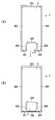
도 9(A)는, 제4의 실시형태에 따른 안테나 장치(104)의 평면도이고, 도 9(B)는 안테나 장치(104)의 정면도이다.
도 10은 제5의 실시형태에 따른 안테나 장치(105)의 분해 사시도이다.
도 11은 제6의 실시형태에 따른 안테나 장치의 비교예인 안테나 장치의, 급전코일(8)의 코일 도체(81)에 흐르는 전류, 부스터 전극 시트(7)의 부스터 전극(71)에 흐르는 전류, 및 그라운드 기판(5)의 그라운드 전극(51)에 흐르는 전류를 각각 나타내는 분해 사시도이다.
도 12는 제6의 실시형태에 따른 안테나 장치(106)의, 급전코일(8)의 코일 도체(81)에 흐르는 전류, 부스터 전극 시트(7)의 부스터 전극(71)에 흐르는 전류, 및 그라운드 기판(5)의 그라운드 전극(51)에 흐르는 전류를 각각 나타내는 분해 사시도이다.
도 13은 제6의 실시형태에 따른 안테나 장치(106)의 평면도이다.1 is a diagram illustrating a state of communication in the proximity of the
2 is an exploded perspective view of the
Fig. 3A is a plan view of the communication terminal device including the
4 shows a current flowing through the
5A and 5B are diagrams showing the relationship between the positional relationship of the
FIG. 6 is a diagram showing a current flowing in each part in a state in which the
7 is an exploded perspective view of the
8 is an exploded perspective view of the
FIG. 9A is a plan view of the
10 is an exploded perspective view of the
11 shows a current flowing through the
12 shows a current flowing through the
13 is a plan view of the
<<제1의 실시형태>>≪ First Embodiment >
제1의 실시형태에 따른 안테나 장치 및 그것을 구비한 통신 단말장치에 대해 도 2~도 6을 참조하여 설명한다.An antenna device and a communication terminal including the same according to the first embodiment will be described with reference to FIGS. 2 to 6.
도 2는 제1의 실시형태에 따른 안테나 장치(101)의 분해 사시도, 도 3(A)는 안테나 장치(101)를 구비한 통신 단말장치의 평면도, 도 3(B)는 그 통신 단말장치의 정면도이다.Fig. 2 is an exploded perspective view of the
본 실시형태에 따른 안테나 모듈은, 예를 들면, FeliCa(등록상표) 등의 NFC(Near Field Communication: 근거리 통신)에 이용되고, 중심 주파수 13.56MHz의 HF대를 이용한다.The antenna module according to the present embodiment is used for NFC (Near Field Communication) such as FeliCa (registered trademark), for example, and uses an HF band having a center frequency of 13.56 MHz.
도 2에 나타내는 안테나 장치(101)는, 상층으로부터 순서대로, 급전코일(8), 부스터 전극 시트(7), 자성체 시트(6), 그라운드 기판(5)을 구비하고 있다. 안테나 장치(101)는 이들의 적층체이다.The
급전코일(8)은, 직사각형 판 형상의 절연기재인 플렉서블 기판(80)에 소용돌이 형상의 코일 도체(81)가 형성된 것이다. 코일 도체(81)는 권회 중심부를 코일 개구부(CW)로 하는 소용돌이 형상으로 형성되어 있다. 코일 개구부(CW)를 가짐으로써, 자계를 이상적으로 방사시킬 수 있다. 플렉서블 기판(80)에는 코일 도체를 외부 회로에 접속하기 위한 접속부(도시하지 않음)가 형성되어 있다.The
또, 코일 도체(81)의 권회수(턴수)는 필요한 인덕턴스에 의해서 정해진다. 원 턴이어도 된다. 그 경우는 단지 루프 형상의 코일 도체가 된다. 또, 하나의 평면상에 형성된 단층 코일이어도 되고, 복수층에 형성된 적층 코일이어도 된다.In addition, the number of turns (number of turns) of the
부스터 전극 시트(7)는, 절연기재(70)와 그 상면에 형성된 부스터 전극(71)으로 구성되어 있다. 부스터 전극(71)은“C”자형의 도체막이며, 급전코일(8)과 대향 배치된다. 부스터 전극 시트(7)는, 평면에서 봤을 때 코일 도체(81)와 포개지는 도체 영역, 코일 개구부(CW)와 포개지는 도체 개구부(비도체 영역)(CA), 및 도체 영역의 외연(外緣)과 도체 개구부(CA)와의 사이를 연접하는 슬릿부(SL1)를 가진다.The
자성체 시트(6)는 예를 들면 시트 형상으로 성형한 페라이트이다. 후에 상술하는 바와 같이, 이 자성체 시트(6)는 부스터 전극(71)의 도체 개구부(CA) 및 슬릿부(SL1)보다 한층 큰 영역을 덮도록 부스터 전극 시트(7)와 포개진다.The
그라운드 기판(5)은, 절연기재(50)와 그 상면에 형성된 그라운드 전극(51)으로 구성되어 있다. 그라운드 전극(51)은 본 발명에 따른 「도체층」에 상당한다. 그라운드 기판(5)으로는, 통신 단말장치의 케이스내에 설치된 프린트 배선판을 이용할 수 있고, 그라운드 전극(51)으로는, 원래 프린트 배선판에 형성되어 있던 그라운드 전극을 이용할 수 있다.The
도 3(A), 도 3(B)에 나타낸 바와 같이, 급전코일(8), 부스터 전극 시트(7), 자성체 시트(6)의 적층체가 그라운드 기판(5)의 한쪽의 짧은 변 주변의 중앙에 배치된다.As shown in FIG. 3 (A) and FIG. 3 (B), the laminated body of the
급전코일(8)은, 그 코일 도체(81)가 부스터 전극(71)의 도체 개구부(CA)를 둘러싸도록, 도체 개구부(CA)의 주위에 배치된다. 이와 같이, 코일 도체(81)가, 부스터 전극(71)의 도체 개구부(CA)를 둘러싸도록 배치하면, 평면에서 봤을 때 코일 도체(81)와 부스터 전극(71)이 포개지는 영역이 커지고, 급전코일(8)과 부스터 전극(71)과의 결합을 보다 강하게 할 수 있다. 부스터 전극(71)의 형상은, 코일 도체(81)의 형상에 맞춰서 설계하는 것이 바람직하다.The
또, 급전코일(8)과 부스터 전극(71)은, 평면에서 봤을 때 코일 도체(81)의 개구부와 부스터 전극(71)의 도체 개구부(CA)가 적어도 일부에서 포개져 있도록 배치되어 있으면 된다.Moreover, the
자성체 시트(6)는, 평면에서 봤을 때, 부스터 전극(71)의 도체 개구부(CA) 및 슬릿부(SL1)보다 한층 큰 영역을 덮도록 배치되어 있다. 즉, 부스터 전극(71)은, 자성체 시트(6)와 포개지는 영역(개구부(CA)나 슬릿(SL1)의 주위)과, 자성체 시트(6)와는 포개지지 않는 영역(외연)을 가진다.The
도 4는, 급전코일(8)의 코일 도체(81)에 흐르는 전류, 부스터 전극 시트(7)의 부스터 전극(71)에 흐르는 전류, 및 그라운드 기판(5)의 그라운드 전극(51)에 흐르는 전류를 각각 나타내는 도면이다. 다만, 이들의 전류는, 급전코일(8), 부스터 전극 시트(7), 자성체 시트(6) 및 그라운드 기판(5)을 적층한 상태에서의 전류이다.4 shows a current flowing through the
도 4에 나타낸 바와 같이, 급전코일(8)의 코일 도체(81)에 전류(EC3)가 흐르면, 코일 도체(81)로부터 생기는 자속이 부스터 전극(71)에 쇄교하려고 하기 때문에, 그 자속을 차단하도록 부스터 전극(71)의 도체 개구부(CA)의 주위에, 코일 도체(81)에 흐르는 전류의 방향과는 반대 방향의 전류(유도 전류)가 생긴다. 도체 개구부(CA)의 주위에 흐르는 전류는, 슬릿부(SL1)의 주위를 통과하고, 부스터 전극(71)의 주위를 따르도록, 즉 부스터 전극(71)의 외연을 주회(周回)하도록 흐른다. 부스터 전극(71)의 주위를 따르도록 전류가 흐름으로써, 자계의 방사 에리어가 넓어지고, 부스터 전극(71)은, 자속 루프를 크게 하는 부스터로서의 역할을 완수한다. 이와 같이, 급전코일(8)의 코일 도체(81)와 부스터 전극(71)은 자계를 주로 결합한다.As shown in FIG. 4, when the current EC3 flows through the
한편, 자성체 시트(6)는 부스터 전극(71)의 도체 개구부(CA) 및 슬릿부(SL1)보다 한층 큰 영역을 덮는다. 그 때문에, 부스터 전극(71)의 도체 개구부(CA)의 주위 및 슬릿부(SL1)의 양옆을 흐르는 전류에 의한 자속이 그라운드 전극(51)과 대부분 쇄교하지 않는다. 바꿔 말하면, 자성체 시트(6)는, 부스터 전극(71)의 도체 개구부(CA)의 주위를 흐르는 전류가 그라운드 전극(51)으로부터 보이지 않도록 숨기고 있다. 즉, 부스터 전극(71)의 도체 개구부(CA)의 주위 및 슬릿부(SL1)의 주위를 흐르는 전류에 의한 유도 전류는 그라운드 전극(51)에 대부분 흐르지 않는다.On the other hand, the
한편, 그라운드 기판(5)의 그라운드 전극(51)에는, 부스터 전극(71)의 외연을 따라서 흐르는 전류(EC22, EC23, EC24)의 유도 전류(EC58, EC57, EC56)가 각각 흐른다. 이것에 수반해, 그라운드 전극(51)의 주위에는, 전류(EC56, EC57, EC58)에 이어서, 전류(EC51, EC52, EC53, EC54, EC55)가 흐른다. 즉, 전류(EC51→EC52→EC53→EC54→EC55→EC56→EC57→EC58)의 경로에서 전류 루프가 생긴다. 이 전류 루프에 의해, 자계의 방사 에리어가 한층 더 넓어져, 자속 루프를 한층 더 크게 할 수 있다.On the other hand, the induced currents EC58, EC57, EC56 of the currents EC22, EC23, EC24 flowing along the outer edge of the
이와 같이, 부스터 전극(71)과 그라운드 전극(51)은 자계를 주로 결합한다.In this way, the
만일 자성체 시트(6)가 없다고 하면, 부스터 전극(71)의 도체 개구부(CA)의 주위를 흐르는 전류 및 슬릿부(SL1)의 양옆을 흐르는 전류의 유도 전류가 그라운드 전극(51)에 흐른다. 이들의 유도 전류는, 부스터 전극(71)의 주위를 흐르는 전류에 의한 유도 전류의 근방이면서, 반대 방향으로 흐르는 전류이기 때문에, 자계가 서로 상쇄되고, 도 4에 나타낸 전류(EC56, EC57, EC58)는 매우 작고, 따라서, 그라운드 전극(51)의 주위에 흐르는 전류(EC51, EC52, EC53, EC54, EC55)도 매우 작은 것이 된다.If there is no
본 예에서는, 도 4에 나타낸 바와 같이, 자성체 시트(6)를 배치함으로써, 상술한 자계의 상쇄 현상이 없고, 그라운드 전극(51)의 외주에 큰 전류가 흐르게 된다.In this example, as shown in FIG. 4, by arranging the
또, 자성체 시트(6)가, 평면에서 봤을 때, 부스터 전극(71)의 도체 개구부에서부터 슬릿부로의 연재 방향으로 삐져나와 있는 것에 의해서, 부스터 전극(71)의 슬릿부(SL1)의 양옆을 흐르는 전류와 그라운드 전극(51)와의 결합이 보다 확실하게 저지되어, 슬릿부(SL1)의 양옆을 흐르는 전류의 유도 전류가 그라운드 전극(51)에 흐르지 않게 하는 것을 보다 확실하게 할 수 있다. 상술한 바와 같이, 이 그라운드 전극(51)에 흐르려고 하는, 슬릿부(SL1)의 주위를 흐르는 전류의 유도 전류는, 전류(EC56, EC57, EC58)와는 반대 방향으로 흐르는 전류이다. 따라서, 자성체 시트(6)가 부스터 전극(71)의 슬릿부(SL1)의 주위를 흐르는 전류의 유도 전류가 그라운드 전극(51)에 흐르는 것을 보다 확실하게 저지할 수 있고, 바꿔 말하면 그라운드 전극(51)의 가장자리 끝을 주회하는 전류가 생기는 것을 막을 수 있고, 부스터 전극(71)의 외주에 큰 전류를 흐르게 할 수 있다.Moreover, when the
도 5(A)는, 제1의 실시형태에 따른 안테나 장치에서의, 그라운드 기판(5)에 대한 자성체 시트(6)의 위치 관계를 나타내고 있다. 도 5(B)는 그 비교예이다. 도 5(B)에 나타낸 바와 같이, 평면에서 봤을 때, 자성체 시트(6)가 그라운드 전극(51)의 주연보다 내측에 있으면, 자성체 시트(6)의 주위를 따라서 흐르는 전류는, 전류 EC56→EC57→EC58→EC59의 루프를 그려 흘러 버린다. 즉 쇼트 컷 전류가 흘러 버린다. 이것에 대해서, 도 5(A)와 같이, 평면에서 봤을 때, 자성체 시트(6)가, 부스터 전극(71)의 도체 개구부에서부터 슬릿의 연재 방향으로, 그라운드 전극(51)의 단연(端緣, end edge)으로부터, 삐져나온 양(T) 만큼 먼 곳에 이르러 있으면, 상기 쇼트 컷이 저지되어, 그라운드 전극(51)의 주위를 흐르는 전류(EC51, EC52, EC53, EC54, EC55)가 커진다. 이것은, 그라운드 전극(51)에 자성체가 근접하고 있으면, 그 부분의 인덕턴스 성분이 커지기 때문이다. 즉, 이 인덕턴스 성분의 높은 영역을 피하고, 그라운드 전극의 주위를 크게 주회하는 경로에서 큰 전류(EC51, EC52, EC53, EC54, EC55)가 흐를 뿐이다. 또, 자성체 시트(6)는, 부스터 전극(71)의 도체 개구부에서부터 슬릿의 연재 방향으로, 그라운드 전극(51)의 단연에 알맞게 도달하고 있어도 된다. 삐져나온 양(T)은, 그라운드 전극(51)에의 자성체 시트(6)의 본딩 위치 정밀도를 고려해 결정하면 된다.FIG. 5A illustrates the positional relationship of the
도 6은, 급전코일(8), 부스터 전극 시트(7), 자성체 시트(6) 및 그라운드 기판(5)을 적층한 상태에서 각 부에 흐르는 전류를 나타내는 도면이다.FIG. 6 is a diagram showing a current flowing in each part in a state in which the
도 6에 나타낸 바와 같이, 코일 도체(81)에 흐르는 전류, 부스터 전극(71)의 주요부(슬릿부(SL1)의 양옆 이외)에 흐르는 전류, 및 그라운드 전극(51)에 흐르는 전류는 동일 방향을 향하고, 이들의 전류에 의해 생기는 자계가 가산된다(각 전류가 서로 무효화되지 않는다). 그 때문에, 급전코일(8) 단독의 경우에 비해, 또 급전코일(8)과 부스터 전극 시트(7)의 조합에 비해, 한층 더 높은 안테나 이득이 얻어진다.As shown in FIG. 6, the current flowing through the
도 3(B)에서 곡선(DG)은, 안테나 장치(101)의 지향 특성을 나타내는 방사 자계 강도의 패턴이다. 이와 같이, 부스터 전극(71)의 슬릿(SL1)이 들어가 있는 방향으로 지향성이 커지고, 그라운드 전극(51)의 중앙에서 보아, 급전코일(8), 부스터 전극 시트(7) 및 자성체 시트(6)의 적층체의 배치 방향의 경사 방향으로 지향성의 중심이 기운다. 이것은, 그라운드 전극(51)에 흐르는 전류의 강도 분포가, 그라운드 전극(51)의 중앙보다 상기 적층체의 배치 위치 가까이에 집중하기 때문이다. 이것은, 그라운드 전극(51)에서 생기는 자계뿐만 아니라, 코일 도체(81) 및 부스터 전극(71)에서 생기는 자계도 방사에 기여하고 있기 때문이다. 따라서, 부스터 전극(71)의 슬릿(SL1)이 휴대전화 단말의 케이스의 선단부를 향하도록 배치하면, 휴대전화 단말끼리를 비스듬히 근접시켜 통신하는 사용법에 적절하다.Curve DG in FIG. 3B is a pattern of radiated magnetic field strength showing directivity of the
또, 제1의 실시형태에서는, 자성체 시트(6)가, 평면에서 봤을 때, 부스터 전극(71)의 도체 개구부(CA) 및 슬릿부(SL1)보다 한층 넓은 범위와 포개지도록 했지만, 부스터 전극(71)의 도체 개구부(CA) 및 슬릿부(SL1)에 딱 맞게 포개지도록 자성체 시트를 형성해도 된다.Moreover, in 1st Embodiment, although the
또, 부스터 전극(71)의 외주위에 흐르는 전류의 방향과 도체 개구부(CA)의 주위에 흐르는 전류의 방향은 반대이므로, 부스터 전극(71)에 흐르는 전류의 강도 분포를 보았을 때, 외주위와 내주위(도체 개구부(CA)의 주위)와의 거의 중간 위치에서 전류 0(제로)의 라인이 생긴다. 이상적으로는 이 전류 0의 라인에 자성체 시트(6)의 외주를 따르도록 자성체 시트(6)의 크기와 위치를 정하면 된다.Moreover, since the direction of the electric current which flows around the outer periphery of the
이와 같이, 부스터 전극(71)이, 평면에서 봤을 때, 자성체 시트(6)와 포개지지 않는 영역(결합 영역)을 가짐으로써, 부스터로서의 역할을 완수한다.In this way, the
또, 본 발명에서는, 그라운드 전극(도체층)(51), 부스터 전극(71), 코일 도체(81)의 모두가 방사 소자로서 기능하지만, 주된 방사 소자는 도체층이다.In addition, although all of the ground electrode (conductor layer) 51, the
<<제2의 실시형태>>≪ Second Embodiment >
도 7은 제2의 실시형태에 따른 안테나 장치(102)의 분해 사시도이다.7 is an exploded perspective view of the
도 7에 나타내는 안테나 장치(102)는, 상층으로부터 순서대로, 급전코일(8), 부스터 전극 시트(7), 자성체 시트(6), 그라운드 기판(5)을 구비하고 있다. 안테나 장치(102)는 이들의 적층체이다.The
제1의 실시형태에서 도 2에 나타낸 안테나 장치(101)와 비교하면, 자성체 시트(6)의 형상이 다르다. 도 7에서 부스터 전극 시트(7)에 자성체 시트(6)가 포개졌을 때의 위치를 2점 쇄선으로 나타내고 있다. 자성체 시트(6)는 부스터 전극(71)의 도체 개구부(CA) 및 슬릿부(SL1)에 포개질 뿐만 아니라, 슬릿부(SL1)에서 분단된 외주 위치에 흐르는 영역, 즉 전류(EC21, EC25)가 흐르는 범위에까지 넓어져 있다.Compared to the
이 구조에 의해, 전류(EC21, EC25)의 유도 전류가 그라운드 전극(51)에 거의 흐르지 않는다. 이 그라운드 전극(51)에 흐르려고 하는, 전류(EC21, EC25)의 유도 전류는, 그 외의 전류(EC51, EC52, EC53, EC54, EC55)와는 반대 방향으로 흐르는 전류이다. 따라서, 자성체 시트(6)가 부스터 전극(71)의 전류(EC21, EC25)의 유도 전류가 그라운드 전극(51)에 흐르는 것을 저지함으로써, 안테나 이득이 더욱 높아진다.By this structure, the induced current of the currents EC21 and EC25 hardly flows to the
<<제3의 실시형태>><< third embodiment >>
도 8은 제3의 실시형태에 따른 안테나 장치(103)의 분해 사시도이다.8 is an exploded perspective view of the
도 8에 나타내는 안테나 장치(103)는, 상층으로부터 순서대로, 부스터 전극 시트(7), 급전코일(8), 자성체 시트(6), 그라운드 기판(5)을 구비하고 있다. 안테나 장치(103)는 이들의 적층체이다.The
제1의 실시형태에서 도 2에 나타낸 안테나 장치(101)와 비교하면, 부스터 전극 시트(7)와 급전코일(8)과의 위치 관계가 반대이다. 이와 같이, 부스터 전극 시트(7)와 자성체 시트(6)과의 사이에 급전코일(8)이 개재하고 있어도 된다. 즉, 부스터 전극(71)의 도체 개구부(CA)의 주위 및 슬릿부(SL1)의 양옆을 흐르는 전류는 자성체 시트(6)가 차폐하고, 부스터 전극(71)의 외주위에 흐르는 전류만이 실질적으로 그라운드 전극(51)에 유도된다.Compared with the
또, 자성체 시트(6)가 급전코일(8)보다 크기 때문에, 급전코일(8)의 코일 도체(81)에 흐르는 전류가 그라운드 전극(51)으로부터 보이지 않게 된다. 즉, 자성체 시트(6)가 코일 도체(81)에 흐르는 전류를 숨긴다. 그 때문에, 무효인(반대 방향의) 유도 전류가 그라운드 전극(51)에 흐르는 것을 방지할 수 있다.In addition, since the
<<제4의 실시형태>><< fourth embodiment >>
도 9(A)는, 제4의 실시형태에 따른 안테나 장치(104)의 평면도, 도 9(B)는 안테나 장치(104)의 정면도이다. 이 예에서는, 급전코일(8), 부스터 전극 시트(7), 자성체 시트(6)의 적층체가 그라운드 기판(5)의 거의 중앙에 배치되어 있다. 부스터 전극 시트(7)에 형성된 부스터 전극(71)의 도체 개구부에서부터 슬릿부(SL1)로의 연재 방향에 자성체 시트(6)가 배치되어 있다. 이 자성체 시트(6)의 선단은 그라운드 기판(5)의 한쪽의 긴 변의 중앙에까지 도달하고 있다.FIG. 9 (A) is a plan view of the
제1의 실시형태에서 도 3(A), 도 3(B)에 나타낸 예와 다른 것은, 급전코일(8), 부스터 전극 시트(7), 자성체 시트(6)의 적층체가 그라운드 기판(5)의 거의 중앙에 배치되어 있는 것과, 그것에 동반해, 자성체 시트(6)가 그라운드 전극(51)의 단연까지 비교적 길게 연장되어 있는 것이다. 또, 자성체 시트(6)가 극단적으로 길어지지 않도록, 부스터 전극(71)의 슬릿부(SL1)를 그라운드 기판(5)의 긴 변 방향에 향해 있다.In the first embodiment, the laminated body of the
도 9(B)에서 곡선(DG)은, 안테나 장치(104)의 지향 특성을 나타내는 방사 자계 강도의 패턴이다. 이와 같이, 급전코일(8), 부스터 전극 시트(7), 자성체 시트(6) 및 그라운드 전극(51)이, 그라운드 전극(51)의 중앙을 중심으로 하는 거의 회전 대칭형이기 때문에, 그라운드 전극(51)의 법선 방향으로 지향성의 중심이 향한다. 이러한 지향 특성은 리더·라이터의 안테나에 대해서 정면으로 대면시켜 이용하는 사용법에 적절하다.Curve DG in FIG. 9B is a pattern of radiated magnetic field strength showing directivity of the
<<제5의 실시형태>><< 5th embodiment >>
도 10은 제5의 실시형태에 따른 안테나 장치(105)의 분해 사시도이다.10 is an exploded perspective view of the
도 10에 나타내는 안테나 장치(105)는, 상층으로부터 순서대로, 급전코일(8), 부스터 전극 시트(7), 자성체 시트(6), 그라운드 기판(5)을 구비하고 있다. 안테나 장치(105)는 이들의 적층체이다.The
제1의 실시형태에서 도 2에 나타낸 안테나 장치(101)와 비교하면, 자성체 시트(6)의 형상이 다르다. 도 10에서 부스터 전극 시트(7)에 자성체 시트(6)가 포개졌을 때의 위치를 2점 쇄선으로 나타내고 있다. 자성체 시트(6)는 부스터 전극(71)의 도체 개구부(CA) 및 슬릿부(SL1)에 포개져 있지만, 슬릿부(SL1)와 포개지는 부분의 폭이 가늘어져 있다.Compared to the
또, 급전코일(8), 부스터 전극 시트(7) 및 자성체 시트(6)의 세트는, 제1의 실시형태와 달리, 그라운드 전극(51)의 가장자리에서부터 중앙 방향으로 멀어진 위치에 배치되어 있다.In addition, unlike the first embodiment, the
이 구조에 의해, 전류(EC21, EC25)의 유도 전류(EC61, EC57)가 그라운드 전극(51)에 흐른다. 자성체 시트(6)는, 슬릿부(SL1)와 포개지는 부분의 폭이 가늘어져 있기 때문에, 자성체 시트(6)의 가늘어져 있는 부분의 양 옆을 전류(EC56, EC62)가 흐른다. 이와 같이, 전류 EC51→EC52→EC53→EC54→EC55→EC56→EC57→EC58→EC59→EC60→EC61→EC62의 경로에서 전류 루프가 생긴다. 이 전류 루프에 의해, 자계의 방사 에리어가 넓어져서, 자속 루프를 크게 할 수 있다.By this structure, the induced currents EC61 and EC57 of the currents EC21 and EC25 flow to the
<<제6의 실시형태>><< 6th embodiment >>
제6의 실시형태에 따른 안테나 장치에 대해서, 도 11~도 13을 참조해 설명한다. 도 11은, 제6의 실시형태에 따른 안테나 장치의 비교예인 안테나 장치의, 급전코일(8)의 코일 도체(81)에 흐르는 전류, 부스터 전극 시트(7)의 부스터 전극(71)에 흐르는 전류, 및 그라운드 기판(5)의 그라운드 전극(51)에 흐르는 전류를 각각 나타내는 분해 사시도이다.The antenna device according to the sixth embodiment will be described with reference to FIGS. 11 to 13. 11 shows a current flowing through the
구조 자체는 제1의 실시형태에서 도 4에 나타낸 것과 동일하지만, 자성체 시트(6)의 전류 차단 효과가 약한 경우, 도 11 중에 파선으로 나타내는 쇼트 컷 전류(EC58)가 흘러 버리는 경우가 있다. 이 경우는 부스터 전극(71)에 흐르는 전류가 만드는 자계를 일부 무효화시키기 때문에, 특성이 열화한다.Although the structure itself is the same as that shown in FIG. 4 in 1st Embodiment, when the electric current interruption effect of the
도 12는, 제6의 실시형태에 따른 안테나 장치(106)의, 급전코일(8)의 코일 도체(81)에 흐르는 전류, 부스터 전극 시트(7)의 부스터 전극(71)에 흐르는 전류, 및 그라운드 기판(5)의 그라운드 전극(51)에 흐르는 전류를 각각 나타내는 분해 사시도이다. 그라운드 전극(51)에는, 도 11에 나타낸 전류(EC58)를 차단하는 위치 및 방향에 슬릿부(SL2)가 형성되어 있다. 이 구조에 의해, 쇼트 컷 전류(EC58)를 확실하게 저지할 수 있다.12 shows a current flowing through the
도 13은 안테나 장치(106)의 평면도이다. 이 도 13에 나타낸 바와 같이, 그라운드 전극(51)의 슬릿부(SL2)는, 부스터 전극(71)의 슬릿부(SL1)의 연재 방향으로 연장하도록 형성되고, 또, 슬릿부(SL1)와 포개지는 위치를 지나는 것이 바람직하다. 또, 슬릿부(SL2)의 길이(L)는, 슬릿부(SL2)의 선단이 도체 개구부(CA)의 내측에 위치하는 길이인 것이 바람직하다. 도 13중의 치수 min는 슬릿부(SL2)의 최단 치수의 예, 치수 max는 슬릿부(SL2)의 최장 치수의 예이다.13 is a plan view of the
이와 같이 그라운드 전극(51)에 슬릿부(SL2)를 형성하면, 필요한 유도 전류를 생기게 함과 동시에 쇼트 컷 전류를 보다 확실하게 저지할 수 있다.By forming the slit portion SL2 in the
또, 안테나 장치의 지향 특성은, 자성체 시트의 형상으로 변화시키는 것도 가능하다. 또, 안테나 장치의 지향 특성은, 슬릿부(SL1)의 형성 위치나, 폭·길이를 조정하여, 변화시킬 수도 있다. 슬릿부(SL1)에서는, 전위차가 크고, 자계가 강하게 방사되기 때문에, 슬릿부의 형성 위치를 변경하여, 지향 특성을 변화시킬 수 있다. 또, 예를 들면, 슬릿부(SL1)의 폭을 작게 하거나, 길이를 길게 하거나 하면, 지향 특성이 향상한다.Moreover, the directivity characteristic of an antenna device can also be changed to the shape of a magnetic body sheet. Moreover, the directivity characteristic of an antenna device can also be changed by adjusting the formation position of slit part SL1, and width and length. In the slit portion SL1, since the potential difference is large and the magnetic field is strongly radiated, the formation position of the slit portion can be changed to change the directivity characteristic. For example, when the width of the slit portion SL1 is reduced or the length is increased, the directivity characteristic is improved.
또, 부스터 전극의 도체 개구부(CA)와 슬릿부(SL1)는, 동일한 폭을 가지고 있어도 된다.In addition, the conductor opening CA and the slit part SL1 of the booster electrode may have the same width.
또, 자성체 시트는 단체(單體)의 소결 페라이트판에 한정되지 않고, 소결 자성체의 양면을 플렉서블 기판 접착용 양면 점착 시트 및 보호용 한 면 점착 시트로 래미네이트한 후, 소결 자성체를 복수의 소편으로 분할한 것을 이용해도 된다. 또, 소결 자성체에 한정되지 않고, 페라이트와 수지와의 복합체나 금속 자성체이어도 된다.In addition, the magnetic sheet is not limited to a single sintered ferrite plate, and after laminating both sides of the sintered magnetic body with the double-sided adhesive sheet for flexible substrate bonding and the protective one-sided adhesive sheet, the sintered magnetic body is divided into a plurality of pieces. You may use the divided thing. Moreover, it is not limited to a sintered magnetic body, The composite of a ferrite and resin, or a magnetic metal body may be sufficient.
이상에 나타낸 각 실시형태에서는, 중심 주파수 13.56MHz의 HF대를 이용하는 안테나 장치를 나타냈지만, 본 발명은 HF대 이외의 주파수대에도 적용할 수 있다. 예를 들면, 900MHz대의 UHF대를 이용하는 RFID 태그용의 안테나로서도 적용할 수 있다. 이 경우는, 급전코일의 코일 도체와 부스터 전극, 부스터 전극과 그라운드 전극은 주로 전자계에서 결합한다.In each of the embodiments described above, an antenna device using an HF band having a center frequency of 13.56 MHz has been described, but the present invention can be applied to frequencies other than the HF band. For example, the present invention can also be applied as an antenna for an RFID tag that uses a UHF band of 900 MHz. In this case, the coil conductor, the booster electrode, the booster electrode, and the ground electrode of the feed coil are mainly coupled in the electromagnetic field.
또, 급전코일과 부스터 전극의 배치 위치는 반대의 관계이어도 된다.In addition, the arrangement position of the feed coil and the booster electrode may be in an opposite relationship.
CA: 도체 개구부
CW: 코일 개구부
SL1, SL2: 슬릿부
5: 그라운드 기판
50: 절연기재
51: 그라운드 전극(도체층)
6: 자성체 시트(자성체층)
7: 부스터 전극 시트
70: 절연기재
71: 부스터 전극
8: 급전코일
80: 플렉서블 기판
81: 코일 도체
101~106: 안테나 장치CA: conductor opening
CW: coil opening
SL1, SL2: Slit section
5: ground substrate
50: insulation material
51: ground electrode (conductor layer)
6: magnetic sheet (magnetic layer)
7: booster electrode sheet
70: insulation material
71: booster electrode
8: feeding coil
80: flexible substrate
81: coil conductor
101-106: antenna device
Claims (8)
Translated fromKorean상기 급전코일과 대향 배치되고, 도체 개구부 및 그 도체 개구부에 연접하는 슬릿부를 가지는 부스터 전극;
상기 급전코일 또는 상기 부스터 전극과 대향 배치된 도체층; 을 구비한 안테나 장치로서,
상기 급전코일 또는 상기 부스터 전극과, 상기 도체층과의 사이에 배치된 자성체층을 더 구비하고,
상기 급전코일, 상기 부스터 전극, 상기 도체층 및 상기 자성체층의 평면시 상태에서, 상기 자성체층은 상기 부스터 전극의 상기 도체 개구부 및 상기 슬릿부에 포개져 있는, 안테나 장치.A feed coil having a loop-shaped or vortex-shaped coil conductor having the winding center portion as a coil opening portion;
A booster electrode disposed to face the feed coil and having a conductor opening and a slit portion connected to the conductor opening;
A conductor layer disposed to face the feed coil or the booster electrode; An antenna device having:
And a magnetic layer disposed between the feed coil or the booster electrode and the conductor layer,
And the magnetic layer is superimposed on the conductor opening and the slit portion of the booster electrode in the planar state of the feed coil, the booster electrode, the conductor layer and the magnetic layer.
상기 급전코일, 상기 부스터 전극, 상기 자성체층 및 상기 도체층의 순서로 대향 배치되어 있는, 안테나 장치.The method of claim 1 or 2, wherein the feed coil, the booster electrode, the conductor layer and the magnetic layer,
And the power supply coil, the booster electrode, the magnetic layer, and the conductor layer in the opposite order.
상기 급전코일 또는 상기 부스터 전극과, 상기 도체층과의 사이에 배치된 자성체층을 더 구비하고,
상기 급전코일, 상기 부스터 전극, 상기 도체층 및 상기 자성체층의 평면시 상태에서, 상기 자성체층은 상기 부스터 전극의 상기 도체 개구부 및 상기 슬릿부에 포개져 있는 것을 특징으로 하는 통신 단말장치.
A feed coil having a loop-shaped or vortex-shaped coil conductor having the winding center portion as a coil opening portion; A booster electrode disposed to face the feed coil and having a conductor opening and a slit portion connected to the conductor opening; A conductor layer disposed to face the feed coil or the booster electrode; A communication terminal having an antenna device having:
And a magnetic layer disposed between the feed coil or the booster electrode and the conductor layer,
And the magnetic layer is superimposed on the conductor opening and the slit of the booster electrode in the planar state of the feed coil, the booster electrode, the conductor layer and the magnetic layer.
Applications Claiming Priority (3)
| Application Number | Priority Date | Filing Date | Title |
|---|---|---|---|
| JP2010091086 | 2010-04-12 | ||
| JPJP-P-2010-091086 | 2010-04-12 | ||
| PCT/JP2011/054088WO2011129151A1 (en) | 2010-04-12 | 2011-02-24 | Antenna device and communication terminal device |
Publications (2)
| Publication Number | Publication Date |
|---|---|
| KR20120099131A KR20120099131A (en) | 2012-09-06 |
| KR101306897B1true KR101306897B1 (en) | 2013-09-10 |
Family
ID=44798530
Family Applications (1)
| Application Number | Title | Priority Date | Filing Date |
|---|---|---|---|
| KR1020127019444AActiveKR101306897B1 (en) | 2010-04-12 | 2011-02-24 | Antenna device and communication terminal device |
Country Status (6)
| Country | Link |
|---|---|
| US (2) | US9595749B2 (en) |
| EP (1) | EP2515377A4 (en) |
| JP (1) | JP4934784B2 (en) |
| KR (1) | KR101306897B1 (en) |
| CN (1) | CN102714355B (en) |
| WO (1) | WO2011129151A1 (en) |
Families Citing this family (54)
| Publication number | Priority date | Publication date | Assignee | Title |
|---|---|---|---|---|
| GB2537773A (en)* | 2010-07-28 | 2016-10-26 | Murata Manufacturing Co | Antenna apparatus and communication terminal instrument |
| CN204189963U (en)* | 2011-07-19 | 2015-03-04 | 株式会社村田制作所 | Antenna assembly and communication terminal |
| JP5609922B2 (en)* | 2011-08-10 | 2014-10-22 | 株式会社村田製作所 | Antenna device and communication terminal device |
| JP5549787B2 (en)* | 2012-02-01 | 2014-07-16 | 株式会社村田製作所 | Antenna device and communication terminal device |
| WO2013156389A1 (en)* | 2012-04-19 | 2013-10-24 | Smartrac Ip B.V. | Integrated loop structure for radio frequency identification |
| JP5772868B2 (en)* | 2012-05-21 | 2015-09-02 | 株式会社村田製作所 | ANTENNA DEVICE AND WIRELESS COMMUNICATION DEVICE |
| GB2543985B (en)* | 2012-06-28 | 2017-10-11 | Murata Manufacturing Co | Antenna device, feed element, and communication terminal device |
| JP5964155B2 (en)* | 2012-06-28 | 2016-08-03 | Necトーキン株式会社 | Antenna device |
| US9083073B2 (en)* | 2012-06-28 | 2015-07-14 | Intel Corporation | Thin chassis near field communication (NFC) antenna integration |
| JP6131418B2 (en)* | 2012-11-26 | 2017-05-24 | スミダコーポレーション株式会社 | Electronics |
| JP2014135448A (en)* | 2013-01-11 | 2014-07-24 | Taiyo Yuden Co Ltd | Electronic component |
| WO2014167812A1 (en)* | 2013-04-12 | 2014-10-16 | パナソニック株式会社 | Antenna, antenna device and communication device |
| US20150009077A1 (en)* | 2013-07-03 | 2015-01-08 | Samsung Electronics Co., Ltd. | Cover of a mobile device and mobile device including the same |
| KR102158858B1 (en)* | 2013-07-03 | 2020-09-22 | 삼성전자주식회사 | Cover of a portable device, and portable device |
| CN205564994U (en)* | 2013-07-16 | 2016-09-07 | 株式会社村田制作所 | Antenna device and communication device |
| CN204809394U (en)* | 2013-08-02 | 2015-11-25 | 株式会社村田制作所 | Antenna device |
| JP6187097B2 (en)* | 2013-09-27 | 2017-08-30 | Tdk株式会社 | Antenna device |
| CN204810312U (en)* | 2013-12-26 | 2015-11-25 | 株式会社村田制作所 | communication terminal device |
| US10461582B2 (en)* | 2014-03-31 | 2019-10-29 | Qualcomm Incorporated | Systems, apparatus, and methods for wireless power receiver coil configuration |
| US10290934B2 (en) | 2014-04-30 | 2019-05-14 | Tdk Corporation | Antenna device |
| JP6318826B2 (en)* | 2014-04-30 | 2018-05-09 | Tdk株式会社 | Antenna device |
| US10009069B2 (en) | 2014-05-05 | 2018-06-26 | Nxp B.V. | Wireless power delivery and data link |
| US10015604B2 (en) | 2014-05-05 | 2018-07-03 | Nxp B.V. | Electromagnetic induction field communication |
| US10014578B2 (en) | 2014-05-05 | 2018-07-03 | Nxp B.V. | Body antenna system |
| WO2015182638A1 (en)* | 2014-05-30 | 2015-12-03 | 株式会社村田製作所 | Antenna device and electronic device |
| US9608327B1 (en)* | 2014-06-24 | 2017-03-28 | Amazon Technologies, Inc. | Magnetically boosted NFC antenna |
| WO2016039584A1 (en)* | 2014-09-12 | 2016-03-17 | 주식회사 아모텍 | Multiple loop antenna module and mobile terminal having same |
| KR101622173B1 (en)* | 2014-10-14 | 2016-05-18 | 주식회사 이엠따블유 | Antenna |
| KR20160063191A (en) | 2014-11-26 | 2016-06-03 | 삼성전기주식회사 | Antenna device and Near field communication device including the same |
| US10014588B2 (en)* | 2014-12-05 | 2018-07-03 | Samsung Electro-Mechanics Co., Ltd. | Near-field antenna apparatus using eddy current and electronic device including the same |
| DE102015102288B4 (en)* | 2015-02-18 | 2019-02-07 | Infineon Technologies Ag | Chip card reader assembly |
| JP2016178527A (en)* | 2015-03-20 | 2016-10-06 | Tdk株式会社 | Antenna device |
| US10554078B2 (en) | 2015-04-24 | 2020-02-04 | Intel Corporation | Method and apparatus for coil integration for uniform wireless charging |
| CN105161819A (en)* | 2015-06-23 | 2015-12-16 | 瑞声精密制造科技(常州)有限公司 | Rfid antenna structure |
| US20170005395A1 (en)* | 2015-06-30 | 2017-01-05 | Tdk Corporation | Antenna device |
| CN104934692B (en)* | 2015-07-02 | 2017-03-22 | 上海安费诺永亿通讯电子有限公司 | NFC/RFID antenna apparatus and mobile terminal thereof |
| CN105024162B (en)* | 2015-07-08 | 2018-06-26 | 深圳市信维通信股份有限公司 | A kind of NFC antenna with metal rear shell |
| CN106410369B (en)* | 2015-07-31 | 2019-11-05 | 比亚迪股份有限公司 | The shell of NFC antenna mould group, mobile terminal and mobile terminal |
| KR102507947B1 (en) | 2015-10-15 | 2023-03-09 | 삼성전자주식회사 | Case and Electronic device including the same |
| US10090592B2 (en)* | 2015-10-29 | 2018-10-02 | Sonitus Technologies Inc. | Communication device |
| US9787368B2 (en)* | 2015-11-06 | 2017-10-10 | Mediatek Inc. | Antenna having passive booster for near field communication |
| US10320086B2 (en)* | 2016-05-04 | 2019-06-11 | Nxp B.V. | Near-field electromagnetic induction (NFEMI) antenna |
| WO2018028486A1 (en)* | 2016-08-08 | 2018-02-15 | Guangdong Oppo Mobile Telecommunications Corp., Ltd. | Housing, method for manufacturing housing, and mobile terminal having housing |
| US10003120B2 (en) | 2016-09-02 | 2018-06-19 | AQ Corporation | Smartphone antenna in flexible PCB |
| USD850424S1 (en) | 2016-12-14 | 2019-06-04 | AQ Corporation | Flexible PCB dual antenna module for use in smartphone |
| US10547112B2 (en) | 2016-09-02 | 2020-01-28 | AQ Corporation | Smartphone antenna in flexible PCB |
| US10074891B2 (en) | 2016-09-02 | 2018-09-11 | AQ Corporation | Smartphone antenna in flexible PCB |
| WO2018113341A1 (en)* | 2016-12-23 | 2018-06-28 | Guangdong Oppo Mobile Telecommunications Corp., Ltd. | Housing assembly for terminal, terminal and mobile phone |
| KR102121795B1 (en)* | 2018-05-04 | 2020-06-11 | 주식회사 아모텍 | Antenna module |
| CN112566440A (en)* | 2019-09-25 | 2021-03-26 | 中兴通讯股份有限公司 | Electronic component and terminal equipment |
| US11303011B2 (en) | 2019-11-27 | 2022-04-12 | AQ Corporation | Smartphone antenna in flexible PCB |
| KR102332612B1 (en)* | 2020-09-11 | 2021-12-01 | 주식회사 이엠따블유 | An antenna module and wireless communication device having the same |
| KR102484949B1 (en)* | 2021-06-22 | 2023-01-10 | 주식회사 썬웨이커뮤니케이션코리아 | Combo type ultra wide band/near frequency communication antenna module |
| CN113869479B (en)* | 2021-09-28 | 2025-03-21 | 上扬无线射频科技扬州有限公司 | A multi-purpose wireless RFID tag suitable for different frequency bands |
Citations (2)
| Publication number | Priority date | Publication date | Assignee | Title |
|---|---|---|---|---|
| KR20080109890A (en)* | 2006-03-31 | 2008-12-17 | 히다치 가세고교 가부시끼가이샤 | Electronic tag |
| JP2009182630A (en) | 2008-01-30 | 2009-08-13 | Dainippon Printing Co Ltd | Booster antenna substrate, booster antenna substrate sheet and non-contact type data carrier device |
Family Cites Families (17)
| Publication number | Priority date | Publication date | Assignee | Title |
|---|---|---|---|---|
| JPH09284038A (en)* | 1996-04-17 | 1997-10-31 | Nhk Spring Co Ltd | Antenna equipment of non-contact data carrier |
| JPH1125244A (en)* | 1997-06-27 | 1999-01-29 | Toshiba Chem Corp | Non-contact data carrier package |
| JP4066520B2 (en)* | 1997-12-18 | 2008-03-26 | 株式会社デンソー | Non-contact IC card reader / writer |
| FR2787640B1 (en)* | 1998-12-22 | 2003-02-14 | Gemplus Card Int | ARRANGEMENT OF AN ANTENNA IN A METALLIC ENVIRONMENT |
| JP3481575B2 (en)* | 2000-09-28 | 2003-12-22 | 寛児 川上 | antenna |
| JP3896965B2 (en)* | 2002-01-17 | 2007-03-22 | 三菱マテリアル株式会社 | Reader / writer antenna and reader / writer equipped with the antenna |
| CN2531458Y (en)* | 2002-03-11 | 2003-01-15 | 上海华虹集成电路有限责任公司 | Non contact type IC card with enhanced induction distance |
| JP3975918B2 (en)* | 2002-09-27 | 2007-09-12 | ソニー株式会社 | Antenna device |
| JP4174801B2 (en)* | 2004-01-15 | 2008-11-05 | 株式会社エフ・イー・シー | Identification tag reader / writer antenna |
| JP4444683B2 (en)* | 2004-02-10 | 2010-03-31 | 株式会社日立製作所 | Semiconductor chip having coiled antenna and communication system using the same |
| JP2006039947A (en)* | 2004-07-27 | 2006-02-09 | Daido Steel Co Ltd | Composite magnetic sheet |
| JP2006085552A (en)* | 2004-09-17 | 2006-03-30 | Oji Paper Co Ltd | Reader and / or writer device |
| JP2006270681A (en) | 2005-03-25 | 2006-10-05 | Sony Corp | Portable equipment |
| JP2007324865A (en) | 2006-05-31 | 2007-12-13 | Sony Chemical & Information Device Corp | Antenna circuit, and transponder |
| JP4796904B2 (en)* | 2006-06-29 | 2011-10-19 | Necカシオモバイルコミュニケーションズ株式会社 | Data communication device |
| JP2008083867A (en)* | 2006-09-26 | 2008-04-10 | Matsushita Electric Works Ltd | Memory card socket |
| CN101897081B (en)* | 2007-12-18 | 2013-02-13 | 株式会社村田制作所 | Magnetic material antenna and antenna device |
- 2011
- 2011-02-24WOPCT/JP2011/054088patent/WO2011129151A1/enactiveApplication Filing
- 2011-02-24KRKR1020127019444Apatent/KR101306897B1/enactiveActive
- 2011-02-24CNCN201180006975.XApatent/CN102714355B/enactiveActive
- 2011-02-24EPEP11768672.5Apatent/EP2515377A4/ennot_activeWithdrawn
- 2011-02-24JPJP2011549098Apatent/JP4934784B2/enactiveActive
- 2012
- 2012-07-26USUS13/558,747patent/US9595749B2/enactiveActive
- 2016
- 2016-12-21USUS15/386,157patent/US9947987B2/enactiveActive
Patent Citations (2)
| Publication number | Priority date | Publication date | Assignee | Title |
|---|---|---|---|---|
| KR20080109890A (en)* | 2006-03-31 | 2008-12-17 | 히다치 가세고교 가부시끼가이샤 | Electronic tag |
| JP2009182630A (en) | 2008-01-30 | 2009-08-13 | Dainippon Printing Co Ltd | Booster antenna substrate, booster antenna substrate sheet and non-contact type data carrier device |
Also Published As
| Publication number | Publication date |
|---|---|
| US9595749B2 (en) | 2017-03-14 |
| JPWO2011129151A1 (en) | 2013-07-11 |
| CN102714355A (en) | 2012-10-03 |
| US9947987B2 (en) | 2018-04-17 |
| US20120306714A1 (en) | 2012-12-06 |
| EP2515377A4 (en) | 2014-12-24 |
| EP2515377A1 (en) | 2012-10-24 |
| JP4934784B2 (en) | 2012-05-16 |
| US20170104259A1 (en) | 2017-04-13 |
| CN102714355B (en) | 2014-07-16 |
| KR20120099131A (en) | 2012-09-06 |
| WO2011129151A1 (en) | 2011-10-20 |
Similar Documents
| Publication | Publication Date | Title |
|---|---|---|
| KR101306897B1 (en) | Antenna device and communication terminal device | |
| JP4993045B2 (en) | ANTENNA DEVICE AND ELECTRONIC DEVICE | |
| KR101789963B1 (en) | Antenna device | |
| JP5115668B2 (en) | ANTENNA DEVICE AND MOBILE COMMUNICATION TERMINAL | |
| JP5742143B2 (en) | Communication terminal equipment | |
| KR20130050633A (en) | Magnetic shielding sheet of hybrid type, antenna device and portable terminal equipment using the same | |
| US20160372817A1 (en) | Antenna device and electronic apparatus | |
| KR101715901B1 (en) | Antenna module | |
| JP2015211422A (en) | Antenna device |
Legal Events
| Date | Code | Title | Description |
|---|---|---|---|
| A201 | Request for examination | ||
| PA0105 | International application | Patent event date:20120723 Patent event code:PA01051R01D Comment text:International Patent Application | |
| PA0201 | Request for examination | ||
| PG1501 | Laying open of application | ||
| E701 | Decision to grant or registration of patent right | ||
| PE0701 | Decision of registration | Patent event code:PE07011S01D Comment text:Decision to Grant Registration Patent event date:20130829 | |
| GRNT | Written decision to grant | ||
| PR0701 | Registration of establishment | Comment text:Registration of Establishment Patent event date:20130904 Patent event code:PR07011E01D | |
| PR1002 | Payment of registration fee | Payment date:20130905 End annual number:3 Start annual number:1 | |
| PG1601 | Publication of registration | ||
| FPAY | Annual fee payment | Payment date:20160829 Year of fee payment:4 | |
| PR1001 | Payment of annual fee | Payment date:20160829 Start annual number:4 End annual number:4 | |
| FPAY | Annual fee payment | Payment date:20170825 Year of fee payment:5 | |
| PR1001 | Payment of annual fee | Payment date:20170825 Start annual number:5 End annual number:5 | |
| PR1001 | Payment of annual fee | Payment date:20200827 Start annual number:8 End annual number:8 | |
| PR1001 | Payment of annual fee | Payment date:20240822 Start annual number:12 End annual number:12 |