KR101304105B1 - Apparatus and method for maintaining immersion fluid in the gap under the projection lens during wafer exchange in an immersion lithography machine - Google Patents
Apparatus and method for maintaining immersion fluid in the gap under the projection lens during wafer exchange in an immersion lithography machineDownload PDFInfo
- Publication number
- KR101304105B1 KR101304105B1KR1020127006824AKR20127006824AKR101304105B1KR 101304105 B1KR101304105 B1KR 101304105B1KR 1020127006824 AKR1020127006824 AKR 1020127006824AKR 20127006824 AKR20127006824 AKR 20127006824AKR 101304105 B1KR101304105 B1KR 101304105B1
- Authority
- KR
- South Korea
- Prior art keywords
- optical member
- substrate
- immersion liquid
- wafer
- immersion
- Prior art date
- Legal status (The legal status is an assumption and is not a legal conclusion. Google has not performed a legal analysis and makes no representation as to the accuracy of the status listed.)
- Expired - Fee Related
Links
Images


Classifications
- H—ELECTRICITY
- H01—ELECTRIC ELEMENTS
- H01L—SEMICONDUCTOR DEVICES NOT COVERED BY CLASS H10
- H01L21/00—Processes or apparatus adapted for the manufacture or treatment of semiconductor or solid state devices or of parts thereof
- H01L21/02—Manufacture or treatment of semiconductor devices or of parts thereof
- H01L21/027—Making masks on semiconductor bodies for further photolithographic processing not provided for in group H01L21/18 or H01L21/34
- H01L21/0271—Making masks on semiconductor bodies for further photolithographic processing not provided for in group H01L21/18 or H01L21/34 comprising organic layers
- H01L21/0273—Making masks on semiconductor bodies for further photolithographic processing not provided for in group H01L21/18 or H01L21/34 comprising organic layers characterised by the treatment of photoresist layers
- H01L21/0274—Photolithographic processes
- G—PHYSICS
- G03—PHOTOGRAPHY; CINEMATOGRAPHY; ANALOGOUS TECHNIQUES USING WAVES OTHER THAN OPTICAL WAVES; ELECTROGRAPHY; HOLOGRAPHY
- G03F—PHOTOMECHANICAL PRODUCTION OF TEXTURED OR PATTERNED SURFACES, e.g. FOR PRINTING, FOR PROCESSING OF SEMICONDUCTOR DEVICES; MATERIALS THEREFOR; ORIGINALS THEREFOR; APPARATUS SPECIALLY ADAPTED THEREFOR
- G03F7/00—Photomechanical, e.g. photolithographic, production of textured or patterned surfaces, e.g. printing surfaces; Materials therefor, e.g. comprising photoresists; Apparatus specially adapted therefor
- G03F7/70—Microphotolithographic exposure; Apparatus therefor
- G03F7/70216—Mask projection systems
- G03F7/70341—Details of immersion lithography aspects, e.g. exposure media or control of immersion liquid supply
- H—ELECTRICITY
- H01—ELECTRIC ELEMENTS
- H01L—SEMICONDUCTOR DEVICES NOT COVERED BY CLASS H10
- H01L21/00—Processes or apparatus adapted for the manufacture or treatment of semiconductor or solid state devices or of parts thereof
- H01L21/02—Manufacture or treatment of semiconductor devices or of parts thereof
- H01L21/027—Making masks on semiconductor bodies for further photolithographic processing not provided for in group H01L21/18 or H01L21/34
- H01L21/0271—Making masks on semiconductor bodies for further photolithographic processing not provided for in group H01L21/18 or H01L21/34 comprising organic layers
- H01L21/0273—Making masks on semiconductor bodies for further photolithographic processing not provided for in group H01L21/18 or H01L21/34 comprising organic layers characterised by the treatment of photoresist layers
- G—PHYSICS
- G03—PHOTOGRAPHY; CINEMATOGRAPHY; ANALOGOUS TECHNIQUES USING WAVES OTHER THAN OPTICAL WAVES; ELECTROGRAPHY; HOLOGRAPHY
- G03F—PHOTOMECHANICAL PRODUCTION OF TEXTURED OR PATTERNED SURFACES, e.g. FOR PRINTING, FOR PROCESSING OF SEMICONDUCTOR DEVICES; MATERIALS THEREFOR; ORIGINALS THEREFOR; APPARATUS SPECIALLY ADAPTED THEREFOR
- G03F7/00—Photomechanical, e.g. photolithographic, production of textured or patterned surfaces, e.g. printing surfaces; Materials therefor, e.g. comprising photoresists; Apparatus specially adapted therefor
- G03F7/70—Microphotolithographic exposure; Apparatus therefor
- G03F7/70691—Handling of masks or workpieces
- G03F7/70716—Stages
- G03F7/70725—Stages control
- G—PHYSICS
- G03—PHOTOGRAPHY; CINEMATOGRAPHY; ANALOGOUS TECHNIQUES USING WAVES OTHER THAN OPTICAL WAVES; ELECTROGRAPHY; HOLOGRAPHY
- G03B—APPARATUS OR ARRANGEMENTS FOR TAKING PHOTOGRAPHS OR FOR PROJECTING OR VIEWING THEM; APPARATUS OR ARRANGEMENTS EMPLOYING ANALOGOUS TECHNIQUES USING WAVES OTHER THAN OPTICAL WAVES; ACCESSORIES THEREFOR
- G03B27/00—Photographic printing apparatus
- G03B27/32—Projection printing apparatus, e.g. enlarger, copying camera
- G03B27/52—Details
- G—PHYSICS
- G03—PHOTOGRAPHY; CINEMATOGRAPHY; ANALOGOUS TECHNIQUES USING WAVES OTHER THAN OPTICAL WAVES; ELECTROGRAPHY; HOLOGRAPHY
- G03F—PHOTOMECHANICAL PRODUCTION OF TEXTURED OR PATTERNED SURFACES, e.g. FOR PRINTING, FOR PROCESSING OF SEMICONDUCTOR DEVICES; MATERIALS THEREFOR; ORIGINALS THEREFOR; APPARATUS SPECIALLY ADAPTED THEREFOR
- G03F7/00—Photomechanical, e.g. photolithographic, production of textured or patterned surfaces, e.g. printing surfaces; Materials therefor, e.g. comprising photoresists; Apparatus specially adapted therefor
- G03F7/20—Exposure; Apparatus therefor
- G03F7/2002—Exposure; Apparatus therefor with visible light or UV light, through an original having an opaque pattern on a transparent support, e.g. film printing, projection printing; by reflection of visible or UV light from an original such as a printed image
- G03F7/2012—Exposure; Apparatus therefor with visible light or UV light, through an original having an opaque pattern on a transparent support, e.g. film printing, projection printing; by reflection of visible or UV light from an original such as a printed image using liquid photohardening compositions, e.g. for the production of reliefs such as flexographic plates or stamps
- G—PHYSICS
- G03—PHOTOGRAPHY; CINEMATOGRAPHY; ANALOGOUS TECHNIQUES USING WAVES OTHER THAN OPTICAL WAVES; ELECTROGRAPHY; HOLOGRAPHY
- G03F—PHOTOMECHANICAL PRODUCTION OF TEXTURED OR PATTERNED SURFACES, e.g. FOR PRINTING, FOR PROCESSING OF SEMICONDUCTOR DEVICES; MATERIALS THEREFOR; ORIGINALS THEREFOR; APPARATUS SPECIALLY ADAPTED THEREFOR
- G03F7/00—Photomechanical, e.g. photolithographic, production of textured or patterned surfaces, e.g. printing surfaces; Materials therefor, e.g. comprising photoresists; Apparatus specially adapted therefor
- G03F7/20—Exposure; Apparatus therefor
- G03F7/2041—Exposure; Apparatus therefor in the presence of a fluid, e.g. immersion; using fluid cooling means
- G—PHYSICS
- G03—PHOTOGRAPHY; CINEMATOGRAPHY; ANALOGOUS TECHNIQUES USING WAVES OTHER THAN OPTICAL WAVES; ELECTROGRAPHY; HOLOGRAPHY
- G03F—PHOTOMECHANICAL PRODUCTION OF TEXTURED OR PATTERNED SURFACES, e.g. FOR PRINTING, FOR PROCESSING OF SEMICONDUCTOR DEVICES; MATERIALS THEREFOR; ORIGINALS THEREFOR; APPARATUS SPECIALLY ADAPTED THEREFOR
- G03F7/00—Photomechanical, e.g. photolithographic, production of textured or patterned surfaces, e.g. printing surfaces; Materials therefor, e.g. comprising photoresists; Apparatus specially adapted therefor
- G03F7/20—Exposure; Apparatus therefor
- G03F7/2051—Exposure without an original mask, e.g. using a programmed deflection of a point source, by scanning, by drawing with a light beam, using an addressed light or corpuscular source
- G03F7/2053—Exposure without an original mask, e.g. using a programmed deflection of a point source, by scanning, by drawing with a light beam, using an addressed light or corpuscular source using a laser
- G03F7/2055—Exposure without an original mask, e.g. using a programmed deflection of a point source, by scanning, by drawing with a light beam, using an addressed light or corpuscular source using a laser for the production of printing plates; Exposure of liquid photohardening compositions
- G—PHYSICS
- G03—PHOTOGRAPHY; CINEMATOGRAPHY; ANALOGOUS TECHNIQUES USING WAVES OTHER THAN OPTICAL WAVES; ELECTROGRAPHY; HOLOGRAPHY
- G03F—PHOTOMECHANICAL PRODUCTION OF TEXTURED OR PATTERNED SURFACES, e.g. FOR PRINTING, FOR PROCESSING OF SEMICONDUCTOR DEVICES; MATERIALS THEREFOR; ORIGINALS THEREFOR; APPARATUS SPECIALLY ADAPTED THEREFOR
- G03F7/00—Photomechanical, e.g. photolithographic, production of textured or patterned surfaces, e.g. printing surfaces; Materials therefor, e.g. comprising photoresists; Apparatus specially adapted therefor
- G03F7/20—Exposure; Apparatus therefor
- G03F7/2051—Exposure without an original mask, e.g. using a programmed deflection of a point source, by scanning, by drawing with a light beam, using an addressed light or corpuscular source
- G03F7/2059—Exposure without an original mask, e.g. using a programmed deflection of a point source, by scanning, by drawing with a light beam, using an addressed light or corpuscular source using a scanning corpuscular radiation beam, e.g. an electron beam
- G03F7/2063—Exposure without an original mask, e.g. using a programmed deflection of a point source, by scanning, by drawing with a light beam, using an addressed light or corpuscular source using a scanning corpuscular radiation beam, e.g. an electron beam for the production of exposure masks or reticles
- G—PHYSICS
- G03—PHOTOGRAPHY; CINEMATOGRAPHY; ANALOGOUS TECHNIQUES USING WAVES OTHER THAN OPTICAL WAVES; ELECTROGRAPHY; HOLOGRAPHY
- G03F—PHOTOMECHANICAL PRODUCTION OF TEXTURED OR PATTERNED SURFACES, e.g. FOR PRINTING, FOR PROCESSING OF SEMICONDUCTOR DEVICES; MATERIALS THEREFOR; ORIGINALS THEREFOR; APPARATUS SPECIALLY ADAPTED THEREFOR
- G03F7/00—Photomechanical, e.g. photolithographic, production of textured or patterned surfaces, e.g. printing surfaces; Materials therefor, e.g. comprising photoresists; Apparatus specially adapted therefor
- G03F7/26—Processing photosensitive materials; Apparatus therefor
- G03F7/30—Imagewise removal using liquid means
- G—PHYSICS
- G03—PHOTOGRAPHY; CINEMATOGRAPHY; ANALOGOUS TECHNIQUES USING WAVES OTHER THAN OPTICAL WAVES; ELECTROGRAPHY; HOLOGRAPHY
- G03F—PHOTOMECHANICAL PRODUCTION OF TEXTURED OR PATTERNED SURFACES, e.g. FOR PRINTING, FOR PROCESSING OF SEMICONDUCTOR DEVICES; MATERIALS THEREFOR; ORIGINALS THEREFOR; APPARATUS SPECIALLY ADAPTED THEREFOR
- G03F7/00—Photomechanical, e.g. photolithographic, production of textured or patterned surfaces, e.g. printing surfaces; Materials therefor, e.g. comprising photoresists; Apparatus specially adapted therefor
- G03F7/70—Microphotolithographic exposure; Apparatus therefor
- G03F7/70691—Handling of masks or workpieces
- G03F7/70716—Stages
- G—PHYSICS
- G03—PHOTOGRAPHY; CINEMATOGRAPHY; ANALOGOUS TECHNIQUES USING WAVES OTHER THAN OPTICAL WAVES; ELECTROGRAPHY; HOLOGRAPHY
- G03F—PHOTOMECHANICAL PRODUCTION OF TEXTURED OR PATTERNED SURFACES, e.g. FOR PRINTING, FOR PROCESSING OF SEMICONDUCTOR DEVICES; MATERIALS THEREFOR; ORIGINALS THEREFOR; APPARATUS SPECIALLY ADAPTED THEREFOR
- G03F7/00—Photomechanical, e.g. photolithographic, production of textured or patterned surfaces, e.g. printing surfaces; Materials therefor, e.g. comprising photoresists; Apparatus specially adapted therefor
- G03F7/70—Microphotolithographic exposure; Apparatus therefor
- G03F7/70691—Handling of masks or workpieces
- G03F7/70733—Handling masks and workpieces, e.g. exchange of workpiece or mask, transport of workpiece or mask
- G—PHYSICS
- G03—PHOTOGRAPHY; CINEMATOGRAPHY; ANALOGOUS TECHNIQUES USING WAVES OTHER THAN OPTICAL WAVES; ELECTROGRAPHY; HOLOGRAPHY
- G03F—PHOTOMECHANICAL PRODUCTION OF TEXTURED OR PATTERNED SURFACES, e.g. FOR PRINTING, FOR PROCESSING OF SEMICONDUCTOR DEVICES; MATERIALS THEREFOR; ORIGINALS THEREFOR; APPARATUS SPECIALLY ADAPTED THEREFOR
- G03F7/00—Photomechanical, e.g. photolithographic, production of textured or patterned surfaces, e.g. printing surfaces; Materials therefor, e.g. comprising photoresists; Apparatus specially adapted therefor
- G03F7/70—Microphotolithographic exposure; Apparatus therefor
- G03F7/708—Construction of apparatus, e.g. environment aspects, hygiene aspects or materials
- G03F7/70808—Construction details, e.g. housing, load-lock, seals or windows for passing light in or out of apparatus
- G03F7/70833—Mounting of optical systems, e.g. mounting of illumination system, projection system or stage systems on base-plate or ground
Landscapes
- Physics & Mathematics (AREA)
- General Physics & Mathematics (AREA)
- Engineering & Computer Science (AREA)
- Condensed Matter Physics & Semiconductors (AREA)
- Manufacturing & Machinery (AREA)
- Computer Hardware Design (AREA)
- Microelectronics & Electronic Packaging (AREA)
- Power Engineering (AREA)
- Health & Medical Sciences (AREA)
- Optics & Photonics (AREA)
- Environmental & Geological Engineering (AREA)
- Epidemiology (AREA)
- Public Health (AREA)
- Toxicology (AREA)
- Exposure And Positioning Against Photoresist Photosensitive Materials (AREA)
- Exposure Of Semiconductors, Excluding Electron Or Ion Beam Exposure (AREA)
- Container, Conveyance, Adherence, Positioning, Of Wafer (AREA)
Abstract
Translated fromKorean
Description
Translated fromKorean본 출원은 "액침 리소그래피용 랜딩 패드 (Landing Pad for Immersion Lithography) "라는 명칭으로 2003년 4월 11일자로 출원한 미국 가출원 제 60/462,499 호에 대한 우선권을 주장하며, 그 내용은 모든 목적용으로 본 명세서에 참고로 포함된다.This application claims priority to US Provisional Application No. 60 / 462,499, filed April 11, 2003, entitled "Landing Pad for Immersion Lithography", the contents of which are incorporated for all purposes. Incorporated herein by reference.
본 발명은 액침 리소그래피 머신에서 웨이퍼 교환동안 투영 렌즈 아래의 갭에서 액침 액체를 유지하는 장치 및 방법에 관한 것이다.The present invention relates to an apparatus and method for retaining immersion liquid in a gap below a projection lens during wafer exchange in an immersion lithography machine.
반도체 프로세싱 동안에 레티클로부터의 이미지를 반도체 웨이퍼 상에 전사하는데 있어서 리소그래피 시스템을 공통으로 이용한다. 통상의 리소그래피 시스템은, 광학 어셈블리, 패턴을 규정하는 레티클을 유지 (holding) 하기 위한 레티클 스테이지, 반도체 웨이퍼를 위치결정하는 웨이퍼 스테이지 어셈블리, 및 레티클과 웨이퍼의 위치를 정밀하게 모니터링하는 측정 시스템을 포함한다. 동작 동안, 레티클에 의해 규정되는 이미지는 광학 어셈블리에 의해 웨이퍼 상으로 투영된다. 투영된 이미지는 전형적으로 웨이퍼 상에서 하나 이상의 다이 (die) 크기를 갖는다. 노광 후에, 웨이퍼 스테이지 어셈블리는 웨이퍼를 이동하고 또 다른 노광을 행한다. 이 프로세스는 웨이퍼 상의 모든 다이들이 노광될 때까지 반복된다. 후속하여, 웨이퍼를 제거하고 그 자리에 새로운 웨이퍼로 대체한다.Lithographic systems are commonly used to transfer images from reticles onto semiconductor wafers during semiconductor processing. Conventional lithography systems include an optical assembly, a reticle stage for holding a reticle defining a pattern, a wafer stage assembly for positioning a semiconductor wafer, and a measurement system for precisely monitoring the position of the reticle and the wafer. . During operation, the image defined by the reticle is projected onto the wafer by the optical assembly. The projected image typically has one or more die sizes on the wafer. After exposure, the wafer stage assembly moves the wafer and performs another exposure. This process is repeated until all the dies on the wafer are exposed. Subsequently, the wafer is removed and replaced with a new wafer in place.
액침 리소그래피 시스템은 웨이퍼 노광 동안 광학 어셈블리와 웨이퍼 사이의 갭을 완전히 채우는 액침 액체층을 활용한다. 광학 어셈블리와 함께 액침 액체의 광 특성은 표준 광학 리소그래피를 이용하여 현재 가능한 최소 배선폭 (feature size) 보다 작은 최소 배선폭의 투영을 가능하게 한다. 예를 들어, 액침 리소그래피는 65 나노미터, 45 나노미터, 및 이 수치를 넘는 수치를 포함하는 차세대 반도체 기술용으로 현재 고려되고 있다. 따라서, 액침 리소그래피는 가까운 미래에 있어서 광 리소그래피를 계속해서 이용할 수 있게 하는 상당한 기술적 돌파구를 나타낸다.The immersion lithography system utilizes an immersion liquid layer that completely fills the gap between the optical assembly and the wafer during wafer exposure. The optical properties of the immersion liquid in combination with the optical assembly allow projection of a minimum wiring width that is less than the minimum feature size currently available using standard optical lithography. For example, immersion lithography is currently being considered for next generation semiconductor technology, including 65 nanometers, 45 nanometers, and numerical values above this. Thus, immersion lithography represents a significant technical breakthrough that continues to enable optical lithography in the near future.
웨이퍼를 노광한 후, 이 웨이퍼를 제거하여 새로운 웨이퍼로 교환한다. 액침 시스템에서 현재 고려되고 있듯이, 액침 액체는 갭으로부터 제거되고 웨이퍼를 교환한 후 다시 채워진다. 상세하게는, 웨이퍼를 교환할 때, 갭으로 유체 공급을 턴오프하고, 유체를 갭으로부터 제거하며 (즉, 진공에 의해 제거하며), 올드 (old) 웨이퍼를 제거하고, 새로운 웨이퍼를 광학 어셈블리 아래에 정렬 및 배치하며, 그 갭을 새로운 액침 액체로 다시 채운다. 일단 상기한 단계들을 모두 완료하게 되면, 그 새로운 웨이퍼의 노광을 시작할 수 있다.After the wafer is exposed, the wafer is removed and replaced with a new wafer. As is currently considered in immersion systems, immersion liquid is removed from the gap and refilled after the wafer is exchanged. Specifically, when swapping wafers, turn off the fluid supply to the gap, remove the fluid from the gap (ie, remove it by vacuum), remove the old wafer, and place the new wafer under the optical assembly. Align and place in, and refill the gap with fresh immersion liquid. Once all of the above steps have been completed, exposure of the new wafer can begin.
상기한 바와 같이 액침 리소그래피에 의한 웨이퍼 교환은 여러 가지 이유로 문제점을 갖고 있다. 갭을 반복하여 채우고 배수함으로 인해 액침 액체의 변동을 야기할 수 있으며 기포를 발생시켜 액침 액체 내에 형성되게 할 수 있다. 기포 및 불안정한 유체는 레티클 상의 이미지를 웨이퍼 상으로 투영할 때 간섭할 수도 있고, 이에 따라 수율이 감소될 수 있다. 또한, 이러한 전체 프로세스는 많은 단계들을 포함하고 시간을 소모하며, 이는 머신 (machine) 의 전체 처리율을 감소시킨다.As described above, wafer exchange by immersion lithography has problems for various reasons. Repeated filling and draining of the gaps can cause fluctuations in the immersion liquid and create bubbles that can form in the immersion liquid. Bubbles and unstable fluid may interfere when projecting the image on the reticle onto the wafer, thereby reducing yield. In addition, this overall process involves many steps and is time consuming, which reduces the overall throughput of the machine.
따라서, 예를 들어, 웨이퍼 교환동안 웨이퍼 스테이지가 투영 렌즈로부터 멀어질 때 투영 렌즈에 인접한 갭에서 액침 액체를 유지하는 장치 및 방법이 필요하다.Accordingly, there is a need for an apparatus and method for maintaining immersion liquid in a gap adjacent to a projection lens, for example, when the wafer stage is away from the projection lens during wafer exchange.
리소그래피 머신에서 투영 렌즈에 인접한 갭에서 액침 액체를 유지하는 장치 및 방법을 개시한다. 이 장치 및 방법은, 피가공물 (work piece) 상에 이미지를 투영하도록 구성된 광학 어셈블리, 및 광학 어셈블리에 인접하는 피가공물을 지지하도록 구성된 피가공물 테이블을 포함하는 스테이지 어셈블리를 포함한다. 환경 시스템에 의해 액침 액체를 갭으로부터 공급 및 제거한다. 피가공물의 노광이 완료된 후, 교환 시스템은 피가공물을 제거하여 제 2 피가공물로 대체한다. 피가공물 테이블이 투영 렌즈로부터 멀어질 때 액침유체 시스템에 의해 갭 내의 액침 액체를 유지한다. 이에 따라 갭은 제 1 피가공물이 제 2 피가공물로 대체될 때 액침 액체로 다시 채워질 필요가 없다.Disclosed are an apparatus and method for maintaining immersion liquid in a gap adjacent a projection lens in a lithography machine. The apparatus and method include a stage assembly comprising an optical assembly configured to project an image onto a work piece and a workpiece table configured to support a workpiece adjacent the optical assembly. The immersion liquid is supplied and removed from the gap by an environmental system. After the exposure of the workpiece is complete, the exchange system removes the workpiece and replaces it with the second workpiece. The immersion liquid is held in the gap by the immersion fluid system when the workpiece table is away from the projection lens. Thus, the gap does not need to be refilled with immersion liquid when the first workpiece is replaced with the second workpiece.
본 발명에 따르면, 웨이퍼 교환 동안 웨이퍼 스테이지가 투영 렌즈로부터 멀어질 때 투영 렌즈에 인접한 갭에서 액침 액체를 유지하는 것이 가능하다.According to the present invention, it is possible to keep the immersion liquid in a gap adjacent to the projection lens when the wafer stage is away from the projection lens during wafer exchange.
도 1 은 본 발명의 특징을 갖는 리소그래피 머신을 나타내는 도면이다.
도 2 는 본 발명의 일 실시형태에 따른 액침 리소그래피 머신의 단면도이다.
도 3a 및 3b 는 본 발명의 다른 일 실시형태에 따른 액침 리소그래피 머신의 단면도 및 상부 정면도이다.
도 4a 및 4b 는 본 발명의 다른 일 실시형태에 따른 액침 리소그래피 머신의 단면도 및 하부 정면도이다.
도 5a 및 5b 는 본 발명의 다른 실시형태들에 따른 2개의 상이한 트윈 웨이퍼 스테이지의 상하부 정면도이다.
도 6a 는 본 발명의 다른 일 실시형태에 따른 트윈 스테이지 리소그래피 머신의 상하부 정면도.
도 6b 내지 6e는 본 발명에 따른 웨이퍼 교환을 나타내는 일련의 도면이다.
도 7a 는 본 발명에 따라 피가공물을 제조하는 공정을 대략 나타내는 흐름도이다.
도 7b 는 피가공물 처리를 보다 상세히 나타내는 흐름도이다.
유사 참조 번호는 도면에서 유사 소자를 나타낸다.BRIEF DESCRIPTION OF THE DRAWINGS Figure 1 is a diagram of a lithographic machine having features of the present invention.
2 is a cross-sectional view of an immersion lithography machine according to one embodiment of the invention.
3A and 3B are cross-sectional and top front views of an immersion lithography machine according to another embodiment of the invention.
4A and 4B are cross-sectional and bottom front views of an immersion lithography machine according to another embodiment of the invention.
5A and 5B are top and bottom front views of two different twin wafer stages in accordance with other embodiments of the present invention.
6A is a top and bottom front view of a twin stage lithography machine according to another embodiment of the present invention.
6B-6E are a series of diagrams illustrating wafer exchange in accordance with the present invention.
7A is a flowchart schematically illustrating a process of manufacturing a workpiece in accordance with the present invention.
7B is a flow chart showing work piece processing in more detail.
Like reference numerals refer to like elements in the drawings.
도 1 은 본 발명의 특징을 갖는 리소그래피 머신 (10) 을 개략적으로 도시한다. 리소그래피 머신 (10) 은 프레임 (12), 조명 시스템 (조사 장치; 14), 광학 어셈블리 (16), 레티클 스테이지 어셈블리 (18), 피가공물 스테이지 어셈블리 (20), 측정 시스템 (22), 제어 시스템 (24), 및 유체 환경 시스템 (26) 을 포함한다. 리소그래피 머신 (10) 의 구성요소들의 설계는 리소그래피 머신 (10) 의 설계 요구 사항에 맞추어 가변될 수 있다.1 schematically depicts a
일 실시형태에서, 리소그래피 머신 (10) 을 이용하여 집적 회로의 패턴 (도시하지 않음) 을 레티클 (28) 로부터 반도체 웨이퍼 (30) (점선으로 표시함) 상에 전송한다. 리소그래피 머신 (10) 은 장착 베이스 (32), 예를 들어 그라운드, 베이스, 플로어 또는 다른 일부 지지 구조에 장착된다.In one embodiment, a
본 발명의 다양한 실시형태에서, 리소그래피 머신 (10) 은 레티클 (28) 과 웨이퍼 (30) 를 동일한 속도로 이동시키면서 레티클 (28) 로부터의 패턴을 웨이퍼 (30) 상에 노광하는 스캐닝 타입 포토리소그래피 시스템으로서 사용될 수 있다. 스캐닝 타입 리소그래피 머신에서, 레티클 (28) 은 레티클 스테이지 어셈블리 (18) 에 의해 광학 어셈블리 (16) 의 광축에 수직으로 이동하게 되고, 웨이퍼 (30) 는 웨이퍼 스테이지 어셈블리 (20) 에 의해 광학 어셈블리 (16) 의 광축에 의해 수직으로 이동하게 된다. 레티클 (28) 및 웨이퍼 (30) 의 스캐닝은 레티클 (28) 및 웨이퍼 (30) 가 동기하여 이동하는 동안 발생한다.In various embodiments of the present invention, the
다른 방법으로, 리소그래피 머신 (10) 은, 레티클 (28) 및 웨이퍼 (30) 가 정지해 있는 동안 레티클 (28) 을 노광하는 스텝 앤 리피트 (step-and-repeat) 타입 포토리소그래피 시스템일 수 있다. 스텝 앤 리피트 공정에서, 웨이퍼 (30) 는 개별적인 필드 노광동안 레티클 (28) 및 광학 어셈블리 (16) 에 대하여 일정한 위치에 있다. 후속하여, 연속하는 노광 단계들 간에, 웨이퍼 (30) 는 웨이퍼 스테이지 어셈블리 (20) 와 함께 광학 어셈블리 (16) 의 광축에 수직하여 연속적으로 이동하게 되어 웨이퍼 (30) 의 다음 필드가 노광을 위해 광학 어셈블리 (16) 및 레티클 (28) 에 대한 위치에 놓이게 된다. 이러한 공정에 따르면, 레티클 (28) 상의 이미지들은 웨이퍼 (30) 의 필드들 상에 순차적으로 노광된 후, 웨이퍼 (30) 의 다음 필드가 광학 어셈블리 (16) 및 레티클 (28) 에 대한 위치에 놓이게 된다.Alternatively,
그러나, 리소그래피 머신 (10) 은 반드시 반도체 제조용 포토리소그래피에만 이용되는 것은 아니다. 리소그래피 머신 (10) 은, 예를 들어, 액정 표시 피가공물 패턴을 직각 유리판 상에 노광하는 LCD 포토리소그래피 시스템, 또는 박막 자기 헤드를 제조하는 포토리소그래피 시스템으로서 이용될 수 있다. 이에 따라, "피가공물" 이라는 용어는 본 명세서에서 일반적으로 리소그래피를 이용하여 패터닝될 수 있는 임의의 장치를 가리키지만, 웨이퍼 또는 LCD 기판으로 제한되지는 않는다.However, the
장치 프레임 (12) 은 리소그래피 머신 (10) 의 구성요소들을 지지한다. 도 1 에 도시한 장치 프레임 (12) 은 장착 베이스 (32) 위에 위치한 레티클 스테이지 어셈블리 (18), 웨이퍼 스테이지 어셈블리 (20), 광학 어셈블리 (16), 및 조명 시스템 (14) 을 지지한다.The
조명 시스템 (14) 은 조명 소스 (34) 및 조명 광학 어셈블리 (36) 를 포함한다. 조명 소스 (34) 는 광 에너지의 빔 (광선) 을 방출한다. 조명 광학 어셈블리 (36) 는 조명 소스 (34) 로부터의 광 에너지의 빔을 광학 어셈블리 (16) 로 유도한다. 빔은 레티클 (28) 의 상이한 부분들을 선택적으로 조명하고 웨이퍼 (30) 를 노광한다. 도 1에서, 조명 소스 (34) 는 레티클 스테이지 어셈블리 (18) 위에서 지지되는 것으로서 도시되어 있다. 그러나, 전형적으로 조명 소스 (34) 는 장치 프레임 (12) 의 측면들 중 하나에 고정되고, 조명 소스 (34) 로부터의 에너지 빔은 조명 광학 어셈블리 (36) 와 함께 레티클 스테이지 어셈블리 (18) 위로 향한다.The
조명 소스 (34) 는 g-라인 소스 (436nm), i-라인 소스 (365nm), KrF 엑시머 레이저 (248nm), ArF 엑시머 레이저 (193nm), 또는 F2 레이저 (157nm) 일 수 있다. 다른 방법으로, 조명 소스 (34) 는 대전된 X-ray를 발생할 수 있다.The
광학 어셈블리 (16) 는 광을 레티클 (28) 을 통과하여 웨이퍼 (30) 로 투영 및/또는 포커싱한다. 리소그래피 머신 (10) 의 설계에 따라, 광학 어셈블리 (16) 는 레티클 (28) 상에 조명된 이미지를 확대 또는 축소할 수 있다. 광학 어셈블리 (16) 가 축소 시스템에 한정될 필요는 없다. 이것은 1x 이상의 확대 시스템일 수도 있다.The
또한, 파장 200nm 이하의 진공 자외선 조사 (VUV) 를 이용하는 노광 피가공물을 이용하는 반사굴절 (catadioptric) 타입의 광학 시스템을 고려할 수 있다. 반사굴절 타입 광 시스템의 예로는, 공개 특허 출원용 공식 간행물에 공개된 일본 특개평 제 10-20195호 및 이에 대응하는 미국 특허번호 제 5,835,275 호 뿐만 아니라 일본 특개평 제8-171054호 및 이에 대응하는 미국 특허번호 제 5,668,672호 가 개시되어 있다. 이들의 경우, 반사 광 피가공물은 빔 스플리터 및 오목 미러를 포함하는 반사굴절 광 시스템일 수 있다. 공개 특허 출원용 공식 간행물에 공개된 일본 특개평 제 10-3039호 및 이에 대응하는 미국 특허번호 제 873,605 호 (출원일: 1997년 12월 6일) 뿐만 아니라 일본 특개평 제 8-334695 호 및 이에 대응하는 미국 특허번호 제 5,689,377 호도 오목 미러 등을 포함하는 반사굴절 타입 광 시스템을 이용한다. 허용되는 범위에서, 상기한 공개 특허 출원용 공식 간행물에 공개된 일본 특허 출원 뿐만 아니라 미국 특허들의 명세서는 참고로 포함된다.Further, a catadioptric type optical system using an exposure workpiece using vacuum ultraviolet irradiation (VUV) having a wavelength of 200 nm or less can be considered. Examples of refraction type optical systems include Japanese Patent Application Laid-Open No. 10-20195 and its corresponding US Patent No. 5,835,275, as well as Japanese Patent Application Laid-open No. Hei 8-171054 and their corresponding publications in the official publication for the patent application. US Patent No. 5,668,672 is disclosed. In these cases, the reflective light workpiece may be a reflective refractive optical system that includes a beam splitter and a concave mirror. Japanese Patent Application Laid-Open No. 10-3039 and its corresponding U.S. Patent No. 873,605 (filed December 6, 1997), as well as Japanese Patent Application Laid-Open No. 8-334695 and its counterpart, published in an official publication for published patent applications. US Patent No. 5,689, 377 also uses a refraction type optical system including a concave mirror or the like. To the extent permitted, the specification of the US patents as well as Japanese patent applications published in the above-mentioned official publications for published patent applications are incorporated by reference.
레티클 스테이지 어셈블리 (18) 는 광학 어셈블리 (16) 및 웨이퍼 (30) 에 대하여 레티클 (28) 을 유지 및 위치결정한다. 일 실시형태에서, 레티클 스테이지 어셈블리 (18) 는 레티클 (28) 을 유지하는 레티클 스테이지 (38), 및 레티클 스테이지 (38) 와 레티클 (28) 을 이동 및 위치시키는 레티클 스테이지 이동기 어셈블리 (40) 를 포함한다.
각 스테이지 이동기 어셈블리 (40, 44) 는 3개의 자유도, 3개 미만의 자유도, 또는 3개 초과의 자유도로 각 스테이지 어셈블리 (38, 42) 를 이동시킬 수 있다. 예를 들어, 다른 실시형태에서, 각 이동기 스테이지 (40, 44) 는 하나 내지 여섯 개의 자유도로 각 스테이지 (38, 42) 를 이동시킬 수 있다. 레티클 스테이지 이동기 어셈블리 (40) 및 피가공물 스테이지 이동기 어셈블리 (44) 의 각각은, 로렌츠력을 활용하여 구동력을 발생하는 회전 모터, 보이스 코일 모터, 선형 모터와 같은 하나 이상의 이동기, 전자기 이동기, 평면 모터, 또는 다른 일부 힘을 이용하는 이동기를 포함할 수 있다.Each
포토리소그래피 시스템 (미국 특허번호 제 5,623,853 호 또는 제 5,528,118 호를 참조하기 바라며, 그 내용은 본 명세서에 참고로 포함됨) 에서, 웨이퍼 스테이지 어셈블리 또는 레티클 스테이지 어셈블리에 선형 모터가 사용되면, 선형 모터는 에어 베어링 (air bearing) 을 이용하는 에어 부상 타입 또는 로렌츠력이나 반작용력을 이용하는 자기 부상 타입일 수 있다. 또한, 스테이지는 가이드를 따라 이동할 수 있거나, 가이드를 이용하지 않는 가이드리스 (guideless) 타입의 스테이지일 수 있다.In photolithography systems (see US Pat. No. 5,623,853 or 5,528,118, the contents of which are incorporated herein by reference), if a linear motor is used in the wafer stage assembly or the reticle stage assembly, the linear motor is an air bearing. It may be an air injury type using air bearing or a magnetic injury type using Lorentz force or reaction force. In addition, the stage may move along a guide or may be a guideless type stage that does not use the guide.
다른 방법으로, 스테이지들 중 하나는 평면 모터에 의해 구동될 수 있으며, 이 평면 모터는 대향하는 위치에 2차원 배열된 코일들을 구비하는 아마추어 (armature) 코일 유닛 및 2차원 배열된 자석들을 구비하는 자석 유닛에 의해 발생하는 전자기력에 의해 그 스테이지를 구동한다. 이러한 타입의 구동 시스템에 의해, 자석 유닛 또는 아마추어 코일 유닛은 스테이지 베이스에 접속되고 나머지 유닛은 그 스테이지의 이동 면측 상에 장착된다.Alternatively, one of the stages can be driven by a planar motor, which is an armature coil unit with coils two-dimensionally arranged in opposite positions and a magnet with two-dimensionally arranged magnets. The stage is driven by the electromagnetic force generated by the unit. By this type of drive system, the magnet unit or armature coil unit is connected to the stage base and the remaining units are mounted on the moving face side of the stage.
상기한 바와 같은 스테이지들의 이동은 포토리소그래피 시스템의 성능에 영향을 끼칠 수 있는 반작용력을 발생한다. 웨이퍼 (기판) 스테이지 이동에 의해 발생되는 반작용력은, 미국 특허번호 제 5,528,100호 및 일본 특개평 제 8-136485호에 설명되어 있는 바와 같이 프레임 부재를 이용함으로써 플로어 (그라운드) 에 기계적으로 전달될 수 있다. 또한, 레티클 (마스크) 스테이지 동작에 의해 발생되는 반작용력은, 미국 특허번호 제 5,874,820 호 및 일본 특개평 제 8-330224 호에 설명되어 있는 바와 같이 프레임 부재를 이용함으로써 플로어 (그라운드) 에 기계적으로 전달될 수 있다. 허용되는 범위에서, 미국 특허번호 제 5,528,100호, 제 5,874,820 호, 및 일본 특개평 제8-330224호는 본 명세서에 참고로 그 내용이 포함된다.Movement of the stages as described above generates a reaction force that can affect the performance of the photolithography system. The reaction forces generated by wafer (substrate) stage movement can be mechanically transmitted to the floor (ground) by using a frame member as described in US Pat. No. 5,528,100 and Japanese Patent Laid-Open No. 8-136485. have. In addition, the reaction forces generated by the reticle (mask) stage operation are mechanically transmitted to the floor (ground) by using a frame member as described in US Pat. No. 5,874,820 and Japanese Patent Laid-Open No. 8-330224. Can be. To the extent permitted, US Pat. Nos. 5,528,100, 5,874,820, and Japanese Patent Application Laid-open No. Hei 8-330224 are incorporated herein by reference.
측정 시스템 (22) 은 광학 어셈블리 (16) 에 대한 또는 다른 일부 기준에 대한 웨이퍼 (30) 및 레티클 (28) 의 움직임을 모니터링한다. 이 정보에 의해, 제어 시스템 (24) 은 레티클 스테이지 어셈블리 (18) 를 제어하여 레티클 (28) 을 정밀하게 위치결정할 수 있고 피가공물 스테이지 어셈블리 (20) 를 제어하여 웨이퍼 (30) 를 정밀하게 위치결정할 수 있다. 측정 시스템 (22) 의 설계는 다양할 수 있다. 예를 들어, 측정 시스템 (22) 은 복수의 레이저 간섭계, 인코더, 미러, 및/또는 다른 측정 디바이스를 활용할 수 있다.The
제어 시스템 (24) 은 측정 시스템 (22) 으로부터 정보를 수신하고 스테이지 이동기 어셈블리 (18, 20) 를 제어하여 레티클 (28) 및 웨이퍼 (30) 를 정밀하게 위치시킨다. 또한, 제어 시스템 (24) 은 환경 시스템 (26) 의 구성요소들의 동작을 제어할 수 있다. 제어 시스템 (24) 은 하나 이상의 프로세서 및 회로를 포함할 수 있다.The
환경 시스템 (26) 은 광학 어셈블리 (16) 와 웨이퍼 (30) 사이의 갭 (도시하지 않음) 에서의 환경을 제어한다. 이 갭은 이미징 필드를 포함한다. 이미징 필드는, 노광되고 있는 웨이퍼 (30) 의 영역에 인접하는 영역, 및 광 에너지의 빔이 광학 어셈블리 (16) 와 웨이퍼 (30) 사이에 이동하는 영역을 포함한다. 이러한 설계에 따라, 환경 시스템 (26) 은 이미징 필드에서의 환경을 제어할 수 있다. 환경 시스템 (26) 에 의해 갭에서 생성되는 그리고/또는 제어되는 원하는 환경은, 웨이퍼 (30) 에 따라 가변될 수 있고 조명 시스템 (14) 을 포함하여 리소그래피 시스템 (10) 의 구성요소들 중 나머지의 설계에 따라 가변될 수 있다. 예를 들어, 원하는 방식으로 제어된 환경은 물 (water) 과 같은 유체일 수 있다. 다른 방법으로, 원하는 제어되는 환경은 가스와 같은 또 다른 타입의 유체일 수 있다. 다양한 실시형태에서, 갭의 범위는 웨이퍼 (30) 의 최상면 및 광학 어셈블리 (16) 의 최종 광 소자 사이의 높이에서 0.1mm 내지 10mm 일 수도 있다.The
일 실시예에서, 환경 시스템 (26) 은 이미징 필드 및 갭의 나머지를 액침 액체로 채운다. 환경 시스템 (26) 및 환경 시스템 (26) 의 구성요소들의 설계는 가변될 수 있다. 다른 실시형태에서, 환경 시스템 (26) 은 스프레이 노즐, 전자 동역학 (electro-kinetic) 스펀지, 다공성 물질 등을 이용하여 액침 액체를 갭 내로 전달 및/또는 주입하고, 진공 펌프, 스펀지 등을 이용하여 갭으로부터 그 유체를 제거한다. 환경 시스템 (26) 의 설계는 가변될 수 있다. 예를 들어, 이것은 갭의 또는 갭 근처의 하나 이상의 위치에서 액침 액체를 주입할 수 있다. 또한, 액침유체 시스템은 피가공물 (30), 광 어셈블리 (16) 의 갭 및/또는 에지 각각의 또는 각각의 근처의 하나 이상의 위치에서 액침 액체의 제거 및/또는 배출 (scavenging) 을 지원할 수 있다. 다양한 환경 시스템에 대한 추가 상세에 대해서는, "Immersion Lithography Fluid Control System"이라는 명칭으로 2003년 4월 9일 출원한 미국 가출원번호 제 60/462,112 호, 및 "Vacuum Ring System and Wick Ring System for Immersion Lithography"라는 명칭으로 2003년 4월 10일자로 출원한 미국 가출원번호 제 60/462,142 호, 및 "Noiseless Fluid Recovery With Porous Material"이라는 명칭으로 2003년 9월 3일 출원한 미국 가출원번호 제 60,500,312호, 및 "Nozzle Design for Immersion Lithography"라는 명칭으로 2004년 2월 2일 출원한 미국 가출원번호 제 60/541,329 호를 참조하기 바라며, 이들 모두의 내용은 본 명세서에 참고로 포함된다.In one embodiment,
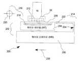
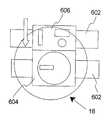
도 2 를 참조하면, 본 발명의 일 실시형태를 나타내는 리소그래피 머신의 단면을 도시하고 있다. 리소그래피 머신 (200) 은, 광학 어셈블리 (16), 및 웨이퍼 테이블 (204) 과 웨이퍼 스테이지 (206) 를 구비하는 스테이지 어셈블리 (202) 를 포함한다. 웨이퍼 테이블 (204) 은 광학 어셈블리 (16) 아래의 웨이퍼 (208) (또는 다른 임의의 타입의 피가공물) 를 지지하도록 구성된다. 광학 어셈블리 (16) 를 둘러싸는 환경 시스템 (26) 은, 웨이퍼 (208) 및 광학 어셈블리 (16) 의 최종 광 소자 사이의 갭으로부터 액침 액체 (212) 를 공급 및 제거하는데 사용된다. 웨이퍼 로더 (loader; 218) (즉, 로봇) 및 정렬 툴 (alignment tool; 220) (즉, 마이크로스코프 및 CCD 카메라) 을 포함하는 피가공물 교환 시스템 (216) 은 웨이퍼 테이블 (204) 상의 웨이퍼 (208) 를 제거하여 제 2 웨이퍼로 대체하도록 구성된다. 이것은 전형적으로 웨이퍼 로더 (218) 를 이용하여 웨이퍼 (208) 를 웨이퍼 테이블 (204) 로부터 들어 올려 제거함으로써 달성된다. 후속하여, 제 2 웨이퍼 (도시하지 않음) 는 웨이퍼 척 (218) 상에 배치되고, 정렬 툴 (220) 을 이용하여 정렬된 후, 웨이퍼 테이블 (204) 의 광학 어셈블리 (16) 아래에 위치결정된다.Referring to FIG. 2, there is shown a cross section of a lithography machine representing one embodiment of the present invention. The
이 실시형태에 따르면, 웨이퍼 스테이지 (206) 는 웨이퍼 교환동안 광학 어셈블리 (16) 의 최종 광 소자에 인접하는 갭에서 액침 액체 (212) 를 유지하도록 구성된 액침 액체 함유 시스템 (214) 을 포함한다. 액침 액체 함유 시스템 (214) 은 웨이퍼 테이블 (204) 에 인접하는 패드 (222) 를 포함한다. 패드 (222) 와 웨이퍼 스테이지 (206) 사이에 설치되는 지지 부재 (224) 를 이용하여 패드 (222) 를 지지한다. 웨이퍼 테이블 (204) 은 웨이퍼 (208) 의 면과 공면인 (coplanar) 평평한 상부면을 구비한다. 또한, 패드 (222) 는 웨이퍼 테이블 (204) 의 상부면 및 웨이퍼 표면과 공면인 평평한 상부면를 구비한다. 패드 (222) 는 웨이퍼 테이블 (204) 에 인접하여 매우 작은 갭 (예를 들어, 0.1 내지 1.0mm) 으로 배열되어 액침 액체 (212) 가 웨이퍼 테이블 (204) 과 패드 (222) 사이에 누출되지 않고 이동가능하다. 웨이퍼 교환동안, 웨이퍼 스테이지 (206) 는 화살표 (226) 방향으로 이동하여 패드 (222) 가 웨이퍼 테이블 (204) 대신에 광학 어셈블리 아래에 위치하여, 갭에서의 유체를 유지하거나 유체 갭의 크기를 유지한다. 새로운 웨이퍼가 정렬된 후, 웨이퍼 스테이지는 다시 원래의 위치로 복귀하여 패드 (222) 가 갭으로부터 제거될 때 제 2 웨이퍼는 광학 어셈블리 (16) 아래에 위치한다. 다양한 실시형태에서, 패드 (222) 는 웨이퍼 테이블 (204) 에 인접하여 갭 없이 연속적으로 배치된다. 웨이퍼 테이블 (204) 이 광학 어셈블리 (16) 아래로부터 이동되기 전에, 웨이퍼 테이블 표면이 패드 표면과 공면이 되도록 웨이퍼 테이블 (204) 의 수직 위치 및/또는 기울기를 조절할 수 있다. 패드 (222) 및 광학 어셈블리 (16) 사이의 갭을 유지하는 것은 단지 웨이퍼 교환 동작에 한정되지 않는다. 패드 (222) 는 정렬 동작 또는 측정 동작 동안 패드 (222) 및 광학 어셈블리 (16) 사이의 공간에서 액침 액체 (212) 를 유지할 정도로 넓을 수 있다. 이들 동작시에, 액침 액체 (212)가 차지하는 영역의 일부는 웨이퍼 테이블 (204) 의 상부면 상에 위치할 수 있다.According to this embodiment, the
도 3a 및 3b 를 참조하면, 본 발명의 다른 실시형태에 따른 액침 리소그래피 머신의 단면도 및 상부 정면도가 도시되어 있다. 리소그래피 머신 (300) 은, 광학 어셈블리 (16), 및 웨이퍼 테이블 (304) 과 웨이퍼 스테이지 (306) 를 구비하는 스테이지 어셈블리 (302) 를 포함한다. 웨이퍼 테이블 (304) 은 광학 어셈블리 (16) 아래에서 웨이퍼 (308) (또는 다른 임의의 타입의 피가공물) 를 지지하도록 구성된다. 광학 어셈블리 (16) 를 둘러싸는 환경 시스템 (26) 은, 웨이퍼 (308) 및 광학 어셈블리 (16) 의 최저 광 소자 사이의 갭으로부터 액침 액체 (312) 를 공급 및 제거하는데 사용된다. 웨이퍼 로더 (318) 및 정렬 툴 (320) 을 포함하는 피가공물 교환 시스템 (316) 은 웨이퍼 테이블 (304) 상의 웨이퍼 (308) 를 제거하여 제 2 웨이퍼로 대체하도록 구성된다. 이것은 웨이퍼 로더 (318) 를 이용하여 웨이퍼 (308) 를 웨이퍼 테이블로부터 제거함으로써 달성된다. 후속하여, 제 2 웨이퍼 (도시하지 않음) 는 웨이퍼 척 (318) 상으로 배치되고, 정렬 툴 (320) 을 이용하여 정렬된 후, 광학 어셈블리 (16) 아래에 위치결정된다. 도 3b 에 가장 잘 도시하고 있듯이, 한 세트의 모터 (322) 를 이용함으로써, 동작시 2개 자유도 (X 및 Y) 로 웨이퍼 테이블 (304) 및 웨이퍼 스테이지 (306) 를 구비하는 웨이퍼 어셈블리 (302) 를 이동한다. 상기한 바와 같이, 모터 (322) 는 선형 모터, 회전 모터, 보이스 코일 모터 등과 같은 임의의 타입의 모터일 수 있다.3A and 3B, a cross sectional and top front view of an immersion lithography machine according to another embodiment of the present invention is shown. The
액침 리소그래피 머신 (300) 은, 광학 어셈블리 아래로부터 웨이퍼 테이블 (304) 이 멀어지는 동안 광학 어셈블리 (16) 아래의 공간에서 액침 액체 (312) 를 유지하도록 구성된 액침 액체 함유 시스템 (324) 도 포함한다. 액침 액체 함유 시스템 (324) 은 패드 (326), 모터 (328), 및 제어 시스템 (330) 을 포함한다. 패드 (326) 는 웨이퍼 테이블 (204) 및 광학 어셈블리 (16) 에 인접하여 위치한다. 웨이퍼 테이블 (304) 은 웨이퍼 (308) 의 면과 공면인 평평한 상부면을 구비한다. 패드 (326) 는 웨이퍼 표면 및 웨이퍼 테이블 (304) 의 상부면과 공면인 평평한 상부면을 구비한다. 패드 (326) 는 제어 시스템 (330) 에 의해 제어되는 모터 (328) 를 이용하여 X 및 Y 방향으로 이동가능하다. 모터 (328) 는 모터 (322) 뿐만 아니라 임의의 타입의 모터일 수 있다. 패드 (326) 는 웨이퍼 테이블 (304; 웨이퍼 스테이지(306)) 이 광학 어셈블리 (16) 아래로부터 멀어질 때 광학 어셈블리 (16) 아래에 위치결정된다. 웨이퍼 교환 동안, 웨이퍼 테이블 (304) 은 광학 어셈블리 (16) 로부터 멀어진다. 동시에, 제어 시스템 (330) 은 광학 어셈블리 (16) 아래의 패드 (326) 를 이동하도록 모터 (328) 에게 지시하여, 웨이퍼 테이블 (308) 을 대체하게 된다. 따라서, 패드 (326) 는 광학 어셈블리 (16) 아래의 갭 내에서 액침 액체 (312) 를 유지한다. 정렬 툴 (320) 을 이용하여 새로운 웨이퍼가 정렬된 후, 웨이퍼 테이블 (304) 은 광학 어셈블리 (16) 아래에 다시 위치한다. 동시에, 제어 시스템 (330) 은 패드 (326) 를 갭으로부터 후퇴하도록 모터에게 지시하여, 액침 액체 (312) 의 누출을 방지한다. 웨이퍼 교환 동작에서, 제어 시스템 (330) 은 웨이퍼 테이블 (304) 및 패드 (326) 사이에 작은 갭을 갖는 상태로 웨이퍼 테이블 (304) 및 패드 (326) 를 이동하는 한편, 광학 어셈블리 (16) 아래의 액침 액체 (312) 는 웨이퍼 테이블 (304) 과 패드 (326) 사이에 이동한다. 따라서, 액침 액체 함유 시스템 (324) 은 웨이퍼 교환 동안 갭으로부터 액침 액체 (312) 를 유지한다. 이 실시형태에서, 웨이퍼 테이블 (304; 웨이퍼 스테이지(306)) 및 패드 (326) 는 개별적으로 이동가능하다. 따라서, 웨이퍼 테이블 (326) 은 자유롭게 이동가능한 한편 액침 액체 (312) 는 패드 (326) 및 광학 어셈블리 (16) 사이의 공간에서 유지된다. 본 발명의 다양한 실시형태에서, 제어 시스템 (330) 은, 별도의 제어 시스템일 수 있거나, 웨이퍼 스테이지 (302) 및 웨이퍼 테이블 (304) 을 위치시키도록 모터 (322) 를 제어하는데 사용되는 제어 시스템 내로 집적될 수 있다. 웨이퍼 테이블 (304) 및 패드 (326) 중 적어도 하나의 수직 위치 및/또는 기울기를 조절하여 웨이퍼 테이블이 광학 어셈블리 (16) 아래로부터 이동하기 전에 웨이퍼 테이블 표면이 패드 표면과 공면이 되게 할 수 있다. 웨이퍼 테이블 (304) 이 광학 어셈블리 (16) 로부터 멀어지는 동작은 반드시 웨이퍼 교환 동작으로만 제한되는 것은 아니다. 예를 들어, 패드 (326) 와 광학 어셈블리 (16) 사이의 공간에서 액침 액체 (312) 를 유지하면서 정렬 동작, 측정 동작, 또는 다른 동작을 실행할 수도 있다.The
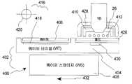
도 4a 및 4b 를 참조하면, 액침 리소그래피 머신의 2개의 단면을 도시하고 있다. 리소그래피 머신 (400) 은 광학 어셈블리 (16), 및 웨이퍼 테이블 (404) 과 웨이퍼 스테이지 (406) 를 구비하는 스테이지 어셈블리 (402) 를 포함한다. 웨이퍼 테이블 (404) 은 광학 어셈블리 (16) 아래의 웨이퍼 (408) (또는 다른 임의의 타입의 피가공물) 를 지지하도록 구성된다. 광학 어셈블리 (16) 를 둘러싸는 환경 시스템 (26) 은, 웨이퍼 (408) 및 광학 어셈블리 (16) 의 최종 광 소자 사이의 갭으로부터 액침 액체 (412) 를 공급 및 제거하는데 사용된다. 웨이퍼 로더 (418) 및 정렬 툴 (420) 을 포함하는 피가공물 교환 시스템 (416) 은, 웨이퍼 테이블 (404) 상의 웨이퍼 (408) 를 제거하여 제 2 웨이퍼로 대체하도록 구성된다. 이것은 웨이퍼 로더 (418) 를 이용하여 웨이퍼 (408) 를 웨이퍼 테이블 (404) 로부터 제거함으로써 달성된다. 후속하여, 제 2 웨이퍼 (도시하지 않음) 는 웨이퍼 척 (418) 상으로 배치되고, 정렬 툴 (420) 을 이용하여 정렬된 후, 도 4a 에 도시한 바와 같이 웨이퍼 테이블 (404) 의 광학 어셈블리 (16) 아래에 위치결정된다.4A and 4B, two cross sections of an immersion lithography machine are shown.
또한, 액침 리소그래피 머신 (400) 은, 광학 어셈블리 (16) 아래로부터 웨이퍼 테이블 (404) 이 멀어지는 동안 광학 어셈블리 (16) 아래의 공간에서 액침 액체 (412) 를 유지하도록 구성된 액침 액체 함유 시스템 (424) 을 포함한다. 액침 액체 함유 시스템 (424) 은 패드 (426), 광학 어셈블리 (16) 상에 설치되는 제 1 클램프 (428), 및 웨이퍼 테이블 (404) 상에 설치되는 제 2 클램프 (430) 를 포함한다. 액침 액체 (412) 가 광학 어셈블리 (16) 및 웨이퍼 테이블 (404) (또는 웨이퍼 (408) ) 간에 존재할 때, 패드 (426) 는 제 2 클램프 (430) 에 의해 웨이퍼 테이블 (404) 상의 제 위치에서 유지된다. 웨이퍼 테이블 (404) 이 광 어셈블리 (16) 로부터 멀어질 때, 예를 들어, 웨이퍼 교환 동작 동안, 패드 (426) 는 웨이퍼 테이블 (404) 로부터 분리되며 제 1 클램프 (428) 에 의해 유지되어 광학 어셈블리 (16) 와 패드 (426) 사이의 액침 액체 (412) 가 유지된다. 웨이퍼 테이블 (404) 은 웨이퍼 (408) 의 표면과 공면인 평평한 상부면을 구비한다. 웨이퍼 테이블 (404) 상에서 유지된 패드 (426) 도 웨이퍼 테이블 (404) 의 상부면 및 웨이퍼 표면과 공면인 평평한 상부면을 구비한다. 따라서, 액침 액체를 누출하지 않고서 광학 어셈블리 아래의 액침 패드 (426) 및 웨이퍼 (408) 를 이동할 수 있다. 다양한 실시형태에서, 클램프 (428 및 430) 는 진공 클램프, 자기 클램프, 정전기 클램프, 또는 기계적 클램프일 수 있다.The
도 4a 에 가장 잘 도시되어 있듯이, 패드 (426) 는 웨이퍼 (408) 노광 동안 웨이퍼 테이블 (404) 상에 위치결정된다. 제 2 클램프 (430) 를 이용하여 웨이퍼 노광 동안 패드 (426) 를 웨이퍼 테이블 (404) 상의 제 위치에 유지하게 된다. 도 4b 에 도시한 바와 같은 웨이퍼 교환 동안, 웨이퍼 테이블 (404) 은 화살표 (432) 방향으로 이동하여 패드 (426) 가 웨이퍼 (408) 대신에 광학 어셈블리 (16) 아래에 위치한다. 이때, 웨이퍼 테이블 (404) 에 대하여 패드 (426) 를 유지하는 제 2 클램프 (430) 가 해제되는 한편 제 1 클램프 (428) 는 광학 어셈블리 (16) 에 대하여 패드 (426) 를 유지한다. 그 결과, 액침 액체 (412) 가 광학 어셈블리 아래에서 유지되는 동안 웨이퍼 (408) 가 교환된다. 새로운 웨이퍼가 정렬된 후, 웨이퍼 테이블 (404) 은 반대 화살표 방향 (432) 으로 이동하게 되어 새로운 웨이퍼가 광학 어셈블리 아래에 위치결정된다. 이러한 이동 전에, 제 1 클램프 (428) 가 해제되는 한편 제 2 클램프 (430) 가 웨이퍼 테이블 (404) 에 대하여 패드 (426) 를 다시 유지한다. 이 실시형태에서, 웨이퍼 테이블 (404) 은 자유롭게 이동가능한 한편 패드 (426) 가 제 1 클램프 (428) 에 의해 클램핑된다.As best shown in FIG. 4A, the
다양한 실시형태에서, 패드 (426) 가 제 1 클램프 (428) 에 의해 클램핑되는 동작은 단지 웨이퍼 교환 동작에 한정되지 않는다. 광학 어셈블리 (16) 및 제 1 클램프 (428) 에 의해 클램핑되는 패드 (426) 사이의 공간에서 액침 액체 (312) 가 유지되는 동안 정렬 동작, 측정 동작, 또는 다른 임의의 동작을 실행할 수 있다. 또한, 클램프 (428) 는 프레임 (12) 이나 다른 지지 부재 상에 설치될 수 있으며, 클램프 (430) 는 웨이퍼 스테이지 (406) 상에 설치될 수 있다. 패드 (426) 는 스테이지 어셈블리 (402) 가 아닌 이동가능한 부재 상에서 유지될 수 있다.In various embodiments, the operation in which the
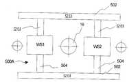
도 5a 및 5b 는 본 발명의 다른 실시형태들에 따른 2개의 상이한 트윈 스테이지 액침 리소그래피 시스템의 상하부 정면도이다. 트윈 스테이지 리소그래피 시스템의 기본 동작 및 구조에 대해서는, 미국특허 제6,262,796호 및 제 6,341,007 호를 참고한다. 허용되는 범위 내에서, 미국 특허 번호 제 6,262,796 호 및 제6,341,007 호의 내용이 본 명세서에 참고로 포함된다. 이들의 양측 실시형태에서는, 한 쌍의 웨이퍼 스테이지 (WS1 및 WS2) 가 도시된다. 모터 (502) 를 이용하여 2개 스테이지 (WS1 및 WS2) 를 수평 방향으로 이동시키거나 위치시키는 반면 모터 (504) 를 이용하여 스테이지 (WS1 및 WS2) 를 수직 방향으로 이동하거나 위치시킨다. 모터 (502, 504) 는 광학 어셈블리 (16) 아래에서 하나의 스테이지를 양자 택일 방식으로 위치결정하는 한편 나머지 스테이지 상에서 웨이퍼 교환 및 정렬을 수행한다. 광학 어셈블리 (16) 아래에서의 웨이퍼 노광이 완료되면, 2개 스테이지는 교환되고 상기한 공정을 반복하게 된다. 이러한 구성에 따라, 도 2 내지 도 4를 참조하여 설명 및 예시한, 광학 어셈블리 (16) 아래의 갭에서의 액침 액체를 유지하는 본 발명의 다양한 실시형태에서는, 2 개 중 1 개의 트윈 스테이지 구성을 이용할 수 있다. 예를 들어 도 2 의 실시형태에 대해서는, 도 5a 또는 5b의 각 웨이퍼 스테이지 (SW1, SW2) 를 수정하여 패드 (222) 및 지지 부재 (224) 를 포함할 수 있다. 도 3 의 실시형태에 대해서는, 단일 패드 (326), 모터 (328), 및 제어 시스템 (330) 을 광학 어셈블리 (16) 에 인접하여 이용할 수 있다. 패드 (326) 는 스테이지 (SW1 및 SW2) 로부터 별도로 이동가능하다. 스테이지 (SW1 및 SW2) 가 교환되는 시기 동안, 패드 (326) 는 광학 어셈블리 (16) 아래로 이동되어 광학 어셈블리 (16) 아래의 액침 액체 (312) 를 유지한다. 마지막으로, 도 4 의 실시형태에서는, 탈착가능한 단일 패드를 이용할 수 있다. 스테이지 (SW1 및 SW2) 가 교환되는 시기 동안, 패드 (426) 를 이용하여 도 4b 에 도시한 바와 같이 갭에서의 액침 액체를 유지한다. 반면에, 노광 동안, 패드는 노광되고 있는 웨이퍼 스테이지 상의 웨이퍼 테이블 상으로 클램핑된다. 이러한 방식으로, 2개 스테이지 (WS1 및 WS2) 용으로 단일 패드만이 필요하다. 다른 방법으로, 후술하는 바와 같이, 제 2 스테이지를 패드로서 이용할 수도 있다.5A and 5B are top and bottom front views of two different twin stage immersion lithography systems, in accordance with other embodiments of the present invention. For the basic operation and structure of twin stage lithography systems, see US Pat. Nos. 6,262,796 and 6,341,007. To the extent permitted, the contents of US Pat. Nos. 6,262,796 and 6,341,007 are incorporated herein by reference. In both of these embodiments, a pair of wafer stages WS1 and WS2 are shown. The
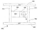
도 6a 를 참조하면, 본 발명을 실시하는 일 실시형태에 따른 트윈 스테이지 리소그래피 머신의 상하부도를 도시하고 있다. 이 실시형태에서, 액침 리소그래피 시스템 (600) 은 제 1 스테이지 (604) 및 제 2 스테이지 (606) 를 포함한다. 2개 스테이지는 모터 (602) 에 의해 X 및 Y 방향으로 이동한다. 이 실시형태에서, 스테이지 (604 및 606) 자신은 갭에서 액침 액체를 함유하는데 사용된다. 이 도에서 도시한 바와 같이 예를 들어, 제 1 스테이지 (604) 는 광학 어셈블리 (16) 아래에 위치결정된다. 피가공물을 교환할 시기에, 모터 (602) 를 이용하여 제 1 스테이지 (604) 에 인접하는 제 2 피가공물와 함께 제 2 스테이지 (606) 를 위치결정된다. 2개 스테이지가 옆으로 나란히 위치결정된 상태에서, 이들은 실질적으로 연속면을 형성한다. 후속하여, 모터 (602) 를 이용하여 2개 스테이지를 일제히 이동하여 제 2 스테이지 (604) 가 광학 어셈블리 (16) 아래에 위치결정되고 제 1 스테이지가 더 이상 광학 어셈블리 (16) 아래에 위치결정되지 않는다. 따라서, 제 1 피가공물이 광학 어셈블리 (16) 로부터 멀어질 때, 갭에서의 액침 액체는, 제 1 스테이지와 실질적으로 연속면을 형성하는 제 2 스테이지 (606) 에 의해 유지된다. 다양한 다른 실시형태에서, 제 2 스테이지 (606) 는, 2 피가공물이 제 1 스테이지 (604) 상으로 배치되는 동안 갭에서의 액침 액체를 유지하는데 사용되는 패드를 포함하는 "패드" 스테이지일 수도 있다. 유사하게, 도 5a 또는 5b에 도시한 모터 구성을 이용할 수 있다.6A, a top and bottom view of a twin stage lithography machine according to one embodiment of practicing the present invention is shown. In this embodiment, the
도 6b 내지 6e 를 참조하면, 본 발명의 일 실시형태에 따른 피가공물 교환을 나타내는 일련의 도면이 도시되어 있다. 도 6b 는 노광이 완료된 후 스테이지 (604) 상의 웨이퍼를 나타낸다. 도 6c 는 광학 어셈블리 (16) 아래에서 제 1 스테이지 (604) 와 접촉하는 (또는 매우 인접하는) 제 2 스테이지 (606) 를 나타낸다. 도 6d 는 전이 발생 위치를 나타내며, 다시 말하면, 제 2 스테이지 (606) 가 광학 어셈블리 (16) 아래에 위치한다. 마지막으로, 도 6e 를 참조하면, 제 1 스테이지 (604) 는 광학 어셈블리 (16) 로부터 멀어진다. 도 6c 및 6d 에 가장 잘 도시되어 있듯이, 2 개 스테이지 (604 및 606) 는 전이 동안 광학 어셈블리 (16) 아래에서 연속면을 제공하고, 따라서 갭에서의 액침 액체를 유지한다. 예시한 이 실시형태에서, 제 2 스테이지 (606) 는 패드 스테이지이다. 그러나, 이 스테이지는 상기한 바와 같이 피가공물 스테이지일 수도 있다.6B-6E, a series of diagrams illustrating a workpiece exchange in accordance with one embodiment of the present invention is shown. 6B shows the wafer on
상기한 다양한 실시형태에서, 패드는 세라믹, 금속 플라스틱과 같은 다수의 상이한 물질로 형성될 수 있다. 이들 물질은 다른 실시형태에 따라 테플론 (Teflon) 으로 코팅될 수도 있다. 또한, 패드 크기는 액침 액체가 차지하는 영역을 커버하도록 충분히 커야 한다. 상기한 다양한 실시형태에서, 광학 어셈블리 (16) 의 최종 광 소자의 표면은 액침 액체 환경 아래에서 일정하여, 유체 마크 (예를 들어, 워터 마크) 의 형성을 방지한다.In the various embodiments described above, the pads can be formed of many different materials, such as ceramics, metal plastics. These materials may be coated with Teflon according to other embodiments. In addition, the pad size should be large enough to cover the area occupied by the immersion liquid. In the various embodiments described above, the surface of the final optical element of the
반도체 웨이퍼는 도 7a 에 도시한 공정에 의해 상기한 시스템들을 이용하여 제조될 수 있다. 단계 (701) 에서, 피가공물의 기능 및 성능 특징을 설계한다. 다음으로 단계 (702) 에서, 이전 설계 단계에 따라 패턴을 갖는 마스크 (레티클) 를 설계하고, 동시에 단계 (703) 에서, 웨이퍼를 실리콘 물질로 형성한다. 단계 (702) 에서 설계된 마스크 패턴을, 본 발명에 따라 상기한 포토리소그래피 시스템에 의해 단계 (704) 에서 단계 (703) 의 웨이퍼 상에 노광한다. 단계 (705) 에서, 반도체 피가공물을 조립 (다이싱 공정, 본딩 공정, 및 패키징 공정을 포함함) 하고, 마지막으로, 단계 (706) 에서 피가공물을 검사한다.The semiconductor wafer can be manufactured using the systems described above by the process shown in FIG. 7A. In
도 7b 는 반도체 피가공물을 제조하는 경우 상기한 단계 (704) 의 상세한 흐름도를 나타낸다. 도 7b 를 참조하면, 단계 (산화 단계; 711) 에서, 웨이퍼 표면이 산화된다. 단계 (CVD 단계; 712) 에서, 웨이퍼 표면 상에 절연막을 형성한다. 단계 (전극 형성 단계; 713) 에서, 증기 증착에 의해 웨이퍼 상에 전극을 형성한다. 단계 (이온 주입 단계; 714) 에서, 이온을 웨이퍼 내에 주입한다. 상기한 단계들 (711 내지 714) 은 웨이퍼 처리 동안 웨이퍼를 위한 전처리 단계들을 형성하고, 처리 요구 사항에 따라 각 단계에서 선택을 행한다.7B shows a detailed flow diagram of
웨이퍼 프로세스의 각 스테이지에서, 상기한 전처리 단계들을 완료하였을 때, 다음에 따르는 후처리 단계들을 구현한다. 후처리 동안, 먼저, 단계 (포토레지스트 형성 단계; 715) 에서, 포토레지스트를 웨이퍼에 도포한다. 다음으로, 단계 (노광 단계; 716) 에서, 상기한 노광 피가공물을 이용하여 마스크 (레티클) 의 회로 패턴을 웨이퍼로 전사한다. 이후, 단계 (현상 단계; 717) 에서, 노광된 웨이퍼를 현상하고, 단계 (에칭 단계; 718) 에서, 잔여 포토레지스트가 아닌 부분들 (즉, 노광된 물질 표면) 을 에칭에 의해 제거한다. 단계 (포토레지스트 제거 단계; 719) 에서, 에칭 후 남아있는 불필요한 포토레지스트를 제거한다.At each stage of the wafer process, upon completion of the above preprocessing steps, the following postprocessing steps are implemented. During post-treatment, first, in step (photoresist formation step; 715), photoresist is applied to the wafer. Next, in step (exposure step) 716, the circuit pattern of the mask (reticle) is transferred to the wafer using the above-described exposed workpiece. Thereafter, in step (development step; 717), the exposed wafer is developed, and in step (etch step; 718), portions other than the remaining photoresist (ie, the exposed material surface) are removed by etching. In step (photoresist removal step; 719), unnecessary photoresist remaining after etching is removed.
이들 전처리 및 후처리 단계들을 반복함으로써 다중 회로를 형성한다.By repeating these pretreatment and posttreatment steps, multiple circuits are formed.
본 명세서에서 설명하고 도시한 바와 같은 특정 리소그래피 머신이 상기한 목적을 충분히 달성하고 있고 이점을 제공할 수 있지만, 이것은 단지 본 발명의 바람직한 실시형태의 예일 뿐이며 청구범위를 제외한 나머지 부분에서의 설계 또는 구성의 상세에 어떠한 제한도 없다는 것을 이해하여야 한다.Although specific lithography machines as described and illustrated herein are fully achieving the above objects and may provide advantages, these are merely examples of preferred embodiments of the present invention and are designed or constructed in other parts than the claims. It should be understood that there are no restrictions on the details of the system.
Claims (48)
Translated fromKorean상기 기판을 재치 (載置) 하는 테이블을 갖는 기판 스테이지와,
상기 테이블과 상이한, 상기 기판 스테이지에 설치되는 부재를 구비하고,
상기 테이블과 상기 부재는 상대 이동 가능하게 상기 기판 스테이지에 설치되고,
상기 테이블과 상기 부재는 각각, 상기 광학 부재와 대향하여 위치됨으로써, 상기 광학 부재 아래에 액침 액체를 유지하고,
상기 테이블과 상기 부재는, 상기 광학 부재와 대향하여 위치되는 상기 테이블의 표면과 상기 부재의 표면이 나란히 배치된 상태에서, 상기 기판 스테이지에 의해 상기 광학 부재에 대해 이동되고, 상기 광학 부재 아래에서 액침 액체는 상기 테이블로부터 상기 부재로 이동하는, 액침 노광 장치.An liquid immersion exposure apparatus for exposing a substrate with an exposure beam through an optical member,
A substrate stage having a table on which the substrate is mounted;
It is provided with a member provided in the said board | substrate stage different from the said table,
The table and the member are installed on the substrate stage to be relatively movable,
The table and the member are respectively positioned to face the optical member, thereby holding the immersion liquid under the optical member,
The table and the member are moved relative to the optical member by the substrate stage in a state where the surface of the table and the surface of the member, which are positioned opposite to the optical member, are arranged side by side, and immersion under the optical member. The liquid immersion exposure apparatus moves from the table to the member.
상기 기판을 재치하는 테이블을 갖는 기판 스테이지와,
상기 테이블과 상이한, 상기 기판 스테이지에 설치되는 부재를 구비하고,
상기 테이블과 상기 부재는 상대 이동 가능하게 상기 기판 스테이지에 설치되고,
상기 광학 부재와 상기 테이블 사이에 액침 액체가 유지되는 제 1 상태로부터, 상기 광학 부재와 상기 부재 사이에 액침 액체가 유지되는 제 2 상태에서 천이되도록, 상기 테이블과 상기 부재는, 상기 기판 스테이지에 의해 상기 광학 부재에 대해 이동되는, 액침 노광 장치.An liquid immersion exposure apparatus for exposing a substrate with an exposure beam through an optical member,
A substrate stage having a table on which the substrate is mounted;
It is provided with a member provided in the said board | substrate stage different from the said table,
The table and the member are installed on the substrate stage to be relatively movable,
The table and the member are moved by the substrate stage such that the transition from the first state in which the immersion liquid is held between the optical member and the table is carried out in a second state in which the immersion liquid is held between the optical member and the member. An immersion exposure apparatus, which is moved relative to the optical member.
상기 테이블과 상기 부재는 서로 접근한 상태에서 상기 광학 부재에 대해 이동되는, 액침 노광 장치.3. The method of claim 2,
And the table and the member are moved relative to the optical member in a state of approaching each other.
상기 테이블과 상기 부재는, 상기 광학 부재와 대향하여 위치되는 상기 테이블의 표면과 상기 부재의 표면이 나란히 배치된 상태에서, 상기 광학 부재에 대해 이동되는, 액침 노광 장치.3. The method of claim 2,
And the table and the member are moved relative to the optical member in a state where the surface of the table and the surface of the member, which are positioned to face the optical member, are arranged side by side.
상기 광학 부재에 대한 상기 테이블과 상기 부재의 이동에 있어서, 상기 광학 부재는 상기 액침 액체와의 접촉이 유지되는, 액침 노광 장치.The method according to any one of claims 1 to 4,
The liquid immersion exposure apparatus of which the contact with the immersion liquid is maintained in the movement of the table and the member with respect to the optical member.
상기 부재는, 상기 테이블이 상기 광학 부재 아래로부터 떨어지기 위하여, 상기 테이블 대신에 상기 광학 부재의 하방에서 액침 액체를 유지하는, 액침 노광 장치.The method of claim 5, wherein
And the member holds the immersion liquid under the optical member instead of the table so that the table falls from below the optical member.
상기 테이블과 상기 부재는, 상기 테이블 대신에 상기 부재가 상기 광학 부재의 하방에서 액침 액체를 유지할 때까지, 상기 광학 부재에 대해 이동되는, 액침 노광 장치.The method of claim 5, wherein
The table and the member are moved relative to the optical member until the member holds the liquid immersion liquid below the optical member instead of the table.
상기 테이블과 상기 부재는, 그 경계가 상기 액침 액체 아래를 통과하도록, 상기 광학 부재에 대해 이동되는, 액침 노광 장치.The method of claim 5, wherein
And the table and the member are moved relative to the optical member such that a boundary thereof passes below the immersion liquid.
상기 테이블과 상기 부재는 근접한 상태, 혹은 갭을 사이에 두고 배치된 상태에서, 상기 광학 부재에 대해 이동되는, 액침 노광 장치.The method of claim 9,
And the table and the member are moved relative to the optical member in a state in which the table and the member are disposed to be adjacent to each other or with a gap therebetween.
상기 테이블과 상기 부재는, 상기 광학 부재 아래에 액침 액체가 유지되도록 근접한 상태에서, 상기 광학 부재에 대해 이동되는, 액침 노광 장치.The method of claim 5, wherein
And the table and the member are moved relative to the optical member in a state where the liquid immersion liquid is held below the optical member.
상기 테이블과 상기 부재는 갭을 사이에 두고 배치된 상태에서 상기 광학 부재에 대해 이동되는, 액침 노광 장치.The method of claim 5, wherein
And the table and the member are moved relative to the optical member while being disposed with a gap therebetween.
상기 테이블과 상기 부재는, 상기 갭이 상기 액침 액체 아래를 통과하도록, 상기 광학 부재에 대해 이동되는, 액침 노광 장치.13. The method of claim 12,
And the table and the member are moved relative to the optical member such that the gap passes under the immersion liquid.
상기 테이블과 상기 부재는, 상기 광학 부재에 대한 이동에 있어서 대향하는 에지가 상기 액침 액체 아래를 통과하도록 이동되는, 액침 노광 장치.The method of claim 5, wherein
The table and the member are immersion exposure apparatus, wherein the opposite edges in the movement with respect to the optical member are moved to pass under the immersion liquid.
상기 테이블과 상기 부재는, 상기 광학 부재에 대해 동시에 이동되는, 액침 노광 장치.The method of claim 5, wherein
And the table and the member are moved simultaneously with respect to the optical member.
상기 테이블과 상기 부재는, 상기 광학 부재에 대한 이동에 있어서 연속하는 표면을 형성하는, 액침 노광 장치.The method of claim 5, wherein
The said table and the said member form the surface which continues in the movement with respect to the said optical member.
상기 기판 스테이지는, 각각 기판을 재치하는, 상기 테이블을 포함하는 2 개의 테이블을 갖고, 상기 2 개의 테이블이 교대로 상기 광학 부재와 대향하여 위치되고,
상기 부재는, 상기 2 개의 테이블의 일방 대신에 상기 광학 부재의 하방에서 액침 액체를 유지함과 함께, 상기 2 개의 테이블의 타방은, 상기 부재 대신에 상기 광학 부재의 하방에서 액침 액체를 유지하는, 액침 노광 장치.The method according to any one of claims 1 to 4,
The substrate stage has two tables each including the table, on which the substrate is placed, the two tables being alternately positioned opposite the optical member,
The member immerses the liquid immersion liquid under the optical member instead of one of the two tables, and the other side of the two tables holds the immersion liquid under the optical member instead of the member. Exposure apparatus.
상기 테이블은, 상기 부재에 의해 상기 광학 부재 아래에 액침 액체가 유지되는 동안, 상기 광학 부재 아래로부터 떨어져, 상기 기판의 노광 동작과 상이한 동작이 실시되는, 액침 노광 장치.The method according to any one of claims 1 to 4,
The table is immersion exposure apparatus in which, while the immersion liquid is held under the optical member by the member, an operation different from that of the exposure operation of the substrate is performed from below the optical member.
상기 상이한 동작은, 상기 기판의 로드와 언로드의 어느 일방 또는 양방을 포함하는, 액침 노광 장치.The method of claim 18,
The different operation includes any one or both of a load and an unload of the substrate.
상기 상이한 동작은, 상기 기판의 얼라이먼트를 포함하는, 액침 노광 장치.The method of claim 19,
And said different operation comprises alignment of said substrate.
상기 기판의 얼라이먼트를 실시하는 얼라이먼트 시스템을, 추가로 구비하고,
상기 부재가 상기 광학 부재와 대향하여 위치되는 동안, 상기 얼라이먼트 시스템에 의해, 상기 테이블에 재치되는 기판의 얼라이먼트가 실시되는, 액침 노광 장치.The method according to any one of claims 1 to 4,
Further provided with an alignment system for performing alignment of the substrate,
And aligning of the substrate placed on the table by the alignment system while the member is positioned opposite the optical member.
상기 테이블에 재치되는 기판을 교환하는 교환 시스템을, 추가로 구비하고,
상기 부재가 상기 광학 부재와 대향하여 위치되는 동안, 상기 교환 시스템에 의해, 상기 테이블에 재치되는 기판의 교환이 실시되는, 액침 노광 장치.The method according to any one of claims 1 to 4,
Further provided with an exchange system which replaces the board | substrate mounted on the said table,
The liquid immersion exposure apparatus, wherein the substrate is placed on the table by the exchange system while the member is positioned opposite the optical member.
상기 테이블이 상기 광학 부재와 대향하여 위치되는 동안, 상기 광학 부재와 상기 액침 액체를 통하여 상기 테이블에 재치되는 기판의 노광이 실시되고,
상기 부재가 상기 광학 부재와 대향하여 위치되는 동안, 상기 교환 시스템에 의해, 상기 테이블에 재치되는 상기 노광된 기판의 교환이 실시되는, 액침 노광 장치.23. The method of claim 22,
While the table is positioned opposite the optical member, exposure of the substrate mounted on the table via the optical member and the immersion liquid is performed,
And, while the member is positioned opposite the optical member, replacement of the exposed substrate placed on the table is effected by the exchange system.
제 1 항 내지 제 4 항 중 어느 한 항에 기재된 액침 노광 장치를 이용하여 피가공물을 노광하는 것과,
상기 노광된 피가공물을 현상하는 것을 포함하는, 디바이스 제조 방법.A device manufacturing method comprising:
Exposing the workpiece using the liquid immersion exposure apparatus according to any one of claims 1 to 4,
A device manufacturing method comprising developing the exposed workpiece.
상기 기판을 재치하는 테이블을 갖는 기판 스테이지에 의해, 상기 테이블에 재치된 기판을 상기 광학 부재와 대향하여 위치시키는 것과,
상기 광학 부재와 액침 액체를 통하여 상기 노광 빔으로 상기 테이블에 재치된 기판을 노광하는 것과,
상기 테이블과, 상기 테이블과 상이하며 상기 테이블과 서로 상대 이동가능한, 상기 기판 스테이지에 설치되는 부재를, 상기 광학 부재와 대향하여 위치되는 상기 테이블의 표면과 상기 부재의 표면이 나란히 배치된 상태에서, 상기 기판 스테이지에 의해 상기 광학 부재에 대해 이동하는 것을 포함하고,
상기 이동에 의해, 상기 광학 부재 아래에서 액침 액체는 상기 테이블로부터 상기 부재로 이동하는, 액침 노광 방법.A liquid immersion exposure method for exposing a substrate with an exposure beam through an optical member,
Positioning the substrate placed on the table so as to face the optical member by a substrate stage having a table on which the substrate is placed;
Exposing the substrate placed on the table with the exposure beam through the optical member and the immersion liquid;
In the state where the surface of the table and the surface of the member, which are opposite to the optical member, are arranged side by side with the table and the member installed on the substrate stage, which are different from the table and relatively movable with the table. Moving relative to the optical member by the substrate stage,
By the movement, the liquid immersion liquid moves from the table to the member under the optical member.
상기 기판을 재치하는 테이블을 갖는 기판 스테이지에 의해, 상기 테이블에 재치된 기판을 상기 광학 부재와 대향하여 위치시키는 것과,
상기 광학 부재와 액침 액체를 통하여 상기 노광 빔으로 상기 테이블에 재치된 기판을 노광하는 것과,
상기 광학 부재와 상기 테이블 사이에 액침 액체가 유지되는 제 1 상태로부터, 상기 광학 부재와, 상기 테이블과 상이한, 상기 기판 스테이지에 설치되는 부재 사이에 액침 액체가 유지되는 제 2 상태로 천이되도록, 서로 상대 이동가능한 상기 테이블과 상기 부재를, 상기 기판 스테이지에 의해 상기 광학 부재에 대해 이동하는 것을 포함하는, 액침 노광 방법.A liquid immersion exposure method for exposing a substrate with an exposure beam through an optical member,
Positioning the substrate placed on the table so as to face the optical member by a substrate stage having a table on which the substrate is placed;
Exposing the substrate placed on the table with the exposure beam through the optical member and the immersion liquid;
From the first state in which the immersion liquid is held between the optical member and the table to transition from the first state in which the immersion liquid is held between the optical member and the member installed on the substrate stage, which is different from the table. And moving said relatively movable table and said member relative to said optical member by said substrate stage.
상기 테이블과 상기 부재는 서로 접근한 상태에서 상기 광학 부재에 대해 이동되는, 액침 노광 방법.The method of claim 26,
And the table and the member are moved relative to the optical member in a state of approaching each other.
상기 테이블과 상기 부재는, 상기 광학 부재와 대향하여 위치되는 상기 테이블의 표면과 상기 부재의 표면이 나란히 배치된 상태에서, 상기 광학 부재에 대해 이동되는, 액침 노광 방법.The method of claim 26,
And the table and the member are moved relative to the optical member in a state where the surface of the table and the surface of the member, which are located opposite to the optical member, are arranged side by side.
상기 광학 부재에 대한 상기 테이블과 상기 부재의 이동에 있어서, 상기 광학 부재는 상기 액침 액체와의 접촉이 유지되는, 액침 노광 방법.29. The method according to any one of claims 25 to 28,
In the movement of the table and the member relative to the optical member, the optical member is maintained in contact with the immersion liquid.
상기 부재는, 상기 테이블이 상기 광학 부재 아래로부터 떨어지기 위하여, 상기 테이블 대신에 상기 광학 부재의 하방에서 액침 액체를 유지하는, 액침 노광 방법.30. The method of claim 29,
And the member holds the immersion liquid below the optical member instead of the table so that the table falls from below the optical member.
상기 테이블과 상기 부재는, 상기 테이블 대신에 상기 부재가 상기 광학 부재의 하방에서 액침 액체를 유지할 때까지, 상기 광학 부재에 대해 이동되는, 액침 노광 방법.30. The method of claim 29,
And the table and the member are moved relative to the optical member until the member holds the liquid immersion liquid below the optical member instead of the table.
상기 테이블과 상기 부재는, 그 경계가 상기 액침 액체 아래를 통과하도록, 상기 광학 부재에 대해 이동되는, 액침 노광 방법.30. The method of claim 29,
And the table and the member are moved relative to the optical member such that a boundary thereof passes under the immersion liquid.
상기 테이블과 상기 부재는 근접한 상태, 혹은 갭을 사이에 두고 배치된 상태에서, 상기 광학 부재에 대해 이동되는, 액침 노광 방법.34. The method of claim 33,
And the table and the member are moved relative to the optical member in a state of being in close proximity or having a gap therebetween.
상기 테이블과 상기 부재는, 상기 광학 부재 아래에 액침 액체가 유지되도록 근접한 상태에서, 상기 광학 부재에 대해 이동되는, 액침 노광 방법.30. The method of claim 29,
And the table and the member are moved relative to the optical member in a state in which the immersion liquid is held below the optical member.
상기 테이블과 상기 부재는 갭을 사이에 두고 배치된 상태에서 상기 광학 부재에 대해 이동되는, 액침 노광 방법.30. The method of claim 29,
And the table and the member are moved relative to the optical member while being disposed with a gap therebetween.
상기 테이블과 상기 부재는, 상기 갭이 상기 액침 액체 아래를 통과하도록, 상기 광학 부재에 대해 이동되는, 액침 노광 방법.The method of claim 36,
And the table and the member are moved relative to the optical member such that the gap passes under the immersion liquid.
상기 테이블과 상기 부재는, 상기 광학 부재에 대한 이동에 있어서 대향하는 에지가 상기 액침 액체 아래를 통과하도록 이동되는, 액침 노광 방법.30. The method of claim 29,
And the table and the member are moved so that an opposite edge in the movement with respect to the optical member passes under the immersion liquid.
상기 테이블과 상기 부재는, 상기 광학 부재에 대해 동시에 이동되는, 액침 노광 방법.30. The method of claim 29,
The table and the member are moved simultaneously with respect to the optical member.
상기 테이블과 상기 부재는, 상기 광학 부재에 대한 이동에 있어서 연속하는 표면을 형성하는, 액침 노광 방법.30. The method of claim 29,
The table and the member form a surface that is continuous in movement with respect to the optical member.
상기 기판 스테이지는, 각각 기판을 재치하는, 상기 테이블을 포함하는 2 개의 테이블을 갖고, 상기 2 개의 테이블이 교대로 상기 광학 부재와 대향하여 위치되고,
상기 부재는, 상기 2 개의 테이블의 일방 대신에 상기 광학 부재의 하방에서 액침 액체를 유지함과 함께, 상기 2 개의 테이블의 타방은, 상기 부재 대신에 상기 광학 부재의 하방에서 액침 액체를 유지하는, 액침 노광 방법.29. The method according to any one of claims 25 to 28,
The substrate stage has two tables each including the table, on which the substrate is placed, the two tables being alternately positioned opposite the optical member,
The member immerses the liquid immersion liquid under the optical member instead of one of the two tables, and the other side of the two tables holds the immersion liquid under the optical member instead of the member. Exposure method.
상기 테이블은, 상기 부재에 의해 상기 광학 부재 아래에 액침 액체가 유지되는 동안, 상기 광학 부재 아래로부터 떨어져, 상기 기판의 노광 동작과 상이한 동작이 실시되는, 액침 노광 방법.29. The method according to any one of claims 25 to 28,
And the table is separated from under the optical member while the liquid immersion liquid is held under the optical member by the member, and an operation different from the exposure operation of the substrate is performed.
상기 상이한 동작은, 상기 기판의 로드와 언로드의 어느 일방 또는 양방을 포함하는, 액침 노광 방법.43. The method of claim 42,
The different operation includes any one or both of a load and an unload of the substrate.
상기 상이한 동작은, 상기 기판의 얼라이먼트를 포함하는, 액침 노광 방법.44. The method of claim 43,
And said different operation comprises alignment of said substrate.
상기 부재가 상기 광학 부재와 대향하여 위치되는 동안, 얼라이먼트 시스템에 의해, 상기 테이블에 재치되는 기판의 얼라이먼트가 실시되는, 액침 노광 방법.29. The method according to any one of claims 25 to 28,
And alignment of the substrate placed on the table by means of an alignment system while the member is positioned opposite the optical member.
상기 부재가 상기 광학 부재와 대향하여 위치되는 동안, 교환 시스템에 의해, 상기 테이블에 재치되는 기판의 교환이 실시되는, 액침 노광 방법.29. The method according to any one of claims 25 to 28,
And, while the member is positioned opposite the optical member, replacement of the substrate placed on the table is performed by an exchange system.
상기 테이블이 상기 광학 부재와 대향하여 위치되는 동안, 상기 광학 부재와 상기 액침 액체를 통하여 상기 테이블에 재치되는 기판의 노광이 실시되고,
상기 부재가 상기 광학 부재와 대향하여 위치되는 동안, 상기 교환 시스템에 의해, 상기 테이블에 재치되는 상기 노광된 기판의 교환이 실시되는, 액침 노광 방법.47. The method of claim 46,
While the table is positioned opposite the optical member, exposure of the substrate mounted on the table via the optical member and the immersion liquid is performed,
And, while the member is positioned opposite the optical member, the exchanging system, on which the exposed substrate is placed on the table, is performed by the exchange system.
제 25 항 내지 제 28 항 중 어느 한 항에 기재된 액침 노광 방법을 이용하여 피가공물을 노광하는 것과,
상기 노광된 피가공물을 현상하는 것을 포함하는, 디바이스 제조 방법.A device manufacturing method comprising:
Exposing the workpiece using the liquid immersion exposure method according to any one of claims 25 to 28;
A device manufacturing method comprising developing the exposed workpiece.
Applications Claiming Priority (3)
| Application Number | Priority Date | Filing Date | Title |
|---|---|---|---|
| US46249903P | 2003-04-11 | 2003-04-11 | |
| US60/462,499 | 2003-04-11 | ||
| PCT/IB2004/001259WO2004090577A2 (en) | 2003-04-11 | 2004-03-17 | Maintaining immersion fluid under a lithographic projection lens |
Related Parent Applications (1)
| Application Number | Title | Priority Date | Filing Date |
|---|---|---|---|
| KR1020057019366ADivisionKR101159564B1 (en) | 2003-04-11 | 2004-03-17 | Apparatus and method for maintaining immersion fluid in the gap under the projection lens during wafer exchange in an immersion lithography machine |
Related Child Applications (1)
| Application Number | Title | Priority Date | Filing Date |
|---|---|---|---|
| KR1020137013439ADivisionKR101498405B1 (en) | 2003-04-11 | 2004-03-17 | Apparatus and method for maintaining immersion fluid in the gap under the projection lens during wafer exchange in an immersion lithography machine |
Publications (2)
| Publication Number | Publication Date |
|---|---|
| KR20120034135A KR20120034135A (en) | 2012-04-09 |
| KR101304105B1true KR101304105B1 (en) | 2013-09-05 |
Family
ID=33159850
Family Applications (15)
| Application Number | Title | Priority Date | Filing Date |
|---|---|---|---|
| KR1020117014236AExpired - Fee RelatedKR101225884B1 (en) | 2003-04-11 | 2004-03-17 | Apparatus and method for maintaining immersion fluid in the gap under the projection lens during wafer exchange in an immersion lithography machine |
| KR1020117014237AExpired - Fee RelatedKR101225829B1 (en) | 2003-04-11 | 2004-03-17 | Apparatus and method for maintaining immersion fluid in the gap under the projection lens during wafer exchange in an immersion lithography machine |
| KR1020187013961AAbandonedKR20180054929A (en) | 2003-04-11 | 2004-03-17 | Apparatus and method for maintaining immersion fluid in the gap under the projection lens during wafer exchange in an immersion lithography machine |
| KR1020177000845AExpired - Fee RelatedKR101861493B1 (en) | 2003-04-11 | 2004-03-17 | Apparatus and method for maintaining immersion fluid in the gap under the projection lens during wafer exchange in an immersion lithography machine |
| KR1020157029869AExpired - Fee RelatedKR101697896B1 (en) | 2003-04-11 | 2004-03-17 | Apparatus and method for maintaining immersion fluid in the gap under the projection lens during wafer exchange in an immersion lithography machine |
| KR1020117031356AExpired - Fee RelatedKR101177332B1 (en) | 2003-04-11 | 2004-03-17 | Apparatus and method for maintaining immersion fluid in the gap under the projection lens during wafer exchange in an immersion lithography machine |
| KR1020057019366AExpired - Fee RelatedKR101159564B1 (en) | 2003-04-11 | 2004-03-17 | Apparatus and method for maintaining immersion fluid in the gap under the projection lens during wafer exchange in an immersion lithography machine |
| KR1020137013439AExpired - Fee RelatedKR101498405B1 (en) | 2003-04-11 | 2004-03-17 | Apparatus and method for maintaining immersion fluid in the gap under the projection lens during wafer exchange in an immersion lithography machine |
| KR1020147022733AExpired - Fee RelatedKR101533206B1 (en) | 2003-04-11 | 2004-03-17 | Apparatus and method for maintaining immersion fluid in the gap under the projection lens during wafer exchange in an immersion lithography machine |
| KR1020117014234AExpired - Fee RelatedKR101178756B1 (en) | 2003-04-11 | 2004-03-17 | Apparatus and method for maintaining immersion fluid in the gap under the projection lens during wafer exchange in an immersion lithography machine |
| KR1020147017763AExpired - Fee RelatedKR101577555B1 (en) | 2003-04-11 | 2004-03-17 | Apparatus and method for maintaining immersion fluid in the gap under the projection lens during wafer exchange in an immersion lithography machine |
| KR1020157002445AExpired - Fee RelatedKR101612681B1 (en) | 2003-04-11 | 2004-03-17 | Apparatus and method for maintaining immersion fluid in the gap under the projection lens during wafer exchange in an immersion lithography machine |
| KR1020147000451AExpired - Fee RelatedKR101475657B1 (en) | 2003-04-11 | 2004-03-17 | Apparatus and method for maintaining immersion fluid in the gap under the projection lens during wafer exchange in an immersion lithography machine |
| KR1020127006824AExpired - Fee RelatedKR101304105B1 (en) | 2003-04-11 | 2004-03-17 | Apparatus and method for maintaining immersion fluid in the gap under the projection lens during wafer exchange in an immersion lithography machine |
| KR1020127006823AExpired - Fee RelatedKR101245031B1 (en) | 2003-04-11 | 2004-03-17 | Apparatus and method for maintaining immersion fluid in the gap under the projection lens during wafer exchange in an immersion lithography machine |
Family Applications Before (13)
| Application Number | Title | Priority Date | Filing Date |
|---|---|---|---|
| KR1020117014236AExpired - Fee RelatedKR101225884B1 (en) | 2003-04-11 | 2004-03-17 | Apparatus and method for maintaining immersion fluid in the gap under the projection lens during wafer exchange in an immersion lithography machine |
| KR1020117014237AExpired - Fee RelatedKR101225829B1 (en) | 2003-04-11 | 2004-03-17 | Apparatus and method for maintaining immersion fluid in the gap under the projection lens during wafer exchange in an immersion lithography machine |
| KR1020187013961AAbandonedKR20180054929A (en) | 2003-04-11 | 2004-03-17 | Apparatus and method for maintaining immersion fluid in the gap under the projection lens during wafer exchange in an immersion lithography machine |
| KR1020177000845AExpired - Fee RelatedKR101861493B1 (en) | 2003-04-11 | 2004-03-17 | Apparatus and method for maintaining immersion fluid in the gap under the projection lens during wafer exchange in an immersion lithography machine |
| KR1020157029869AExpired - Fee RelatedKR101697896B1 (en) | 2003-04-11 | 2004-03-17 | Apparatus and method for maintaining immersion fluid in the gap under the projection lens during wafer exchange in an immersion lithography machine |
| KR1020117031356AExpired - Fee RelatedKR101177332B1 (en) | 2003-04-11 | 2004-03-17 | Apparatus and method for maintaining immersion fluid in the gap under the projection lens during wafer exchange in an immersion lithography machine |
| KR1020057019366AExpired - Fee RelatedKR101159564B1 (en) | 2003-04-11 | 2004-03-17 | Apparatus and method for maintaining immersion fluid in the gap under the projection lens during wafer exchange in an immersion lithography machine |
| KR1020137013439AExpired - Fee RelatedKR101498405B1 (en) | 2003-04-11 | 2004-03-17 | Apparatus and method for maintaining immersion fluid in the gap under the projection lens during wafer exchange in an immersion lithography machine |
| KR1020147022733AExpired - Fee RelatedKR101533206B1 (en) | 2003-04-11 | 2004-03-17 | Apparatus and method for maintaining immersion fluid in the gap under the projection lens during wafer exchange in an immersion lithography machine |
| KR1020117014234AExpired - Fee RelatedKR101178756B1 (en) | 2003-04-11 | 2004-03-17 | Apparatus and method for maintaining immersion fluid in the gap under the projection lens during wafer exchange in an immersion lithography machine |
| KR1020147017763AExpired - Fee RelatedKR101577555B1 (en) | 2003-04-11 | 2004-03-17 | Apparatus and method for maintaining immersion fluid in the gap under the projection lens during wafer exchange in an immersion lithography machine |
| KR1020157002445AExpired - Fee RelatedKR101612681B1 (en) | 2003-04-11 | 2004-03-17 | Apparatus and method for maintaining immersion fluid in the gap under the projection lens during wafer exchange in an immersion lithography machine |
| KR1020147000451AExpired - Fee RelatedKR101475657B1 (en) | 2003-04-11 | 2004-03-17 | Apparatus and method for maintaining immersion fluid in the gap under the projection lens during wafer exchange in an immersion lithography machine |
Family Applications After (1)
| Application Number | Title | Priority Date | Filing Date |
|---|---|---|---|
| KR1020127006823AExpired - Fee RelatedKR101245031B1 (en) | 2003-04-11 | 2004-03-17 | Apparatus and method for maintaining immersion fluid in the gap under the projection lens during wafer exchange in an immersion lithography machine |
Country Status (9)
| Country | Link |
|---|---|
| US (18) | US7372538B2 (en) |
| EP (8) | EP3141953A3 (en) |
| JP (12) | JP4315198B2 (en) |
| KR (15) | KR101225884B1 (en) |
| CN (3) | CN101980086B (en) |
| IL (5) | IL170735A (en) |
| SG (12) | SG139734A1 (en) |
| TW (16) | TWI545387B (en) |
| WO (1) | WO2004090577A2 (en) |
Families Citing this family (222)
| Publication number | Priority date | Publication date | Assignee | Title |
|---|---|---|---|---|
| EP1420299B1 (en) | 2002-11-12 | 2011-01-05 | ASML Netherlands B.V. | Immersion lithographic apparatus and device manufacturing method |
| US10503084B2 (en) | 2002-11-12 | 2019-12-10 | Asml Netherlands B.V. | Lithographic apparatus and device manufacturing method |
| US7372541B2 (en) | 2002-11-12 | 2008-05-13 | Asml Netherlands B.V. | Lithographic apparatus and device manufacturing method |
| DE60335595D1 (en) | 2002-11-12 | 2011-02-17 | Asml Netherlands Bv | Immersion lithographic apparatus and method of making a device |
| CN100568101C (en) | 2002-11-12 | 2009-12-09 | Asml荷兰有限公司 | Photolithography apparatus and device manufacturing method |
| US7110081B2 (en) | 2002-11-12 | 2006-09-19 | Asml Netherlands B.V. | Lithographic apparatus and device manufacturing method |
| KR100585476B1 (en) | 2002-11-12 | 2006-06-07 | 에이에스엠엘 네델란즈 비.브이. | Lithographic Apparatus and Device Manufacturing Method |
| US9482966B2 (en) | 2002-11-12 | 2016-11-01 | Asml Netherlands B.V. | Lithographic apparatus and device manufacturing method |
| SG121822A1 (en)* | 2002-11-12 | 2006-05-26 | Asml Netherlands Bv | Lithographic apparatus and device manufacturing method |
| KR101101737B1 (en) | 2002-12-10 | 2012-01-05 | 가부시키가이샤 니콘 | Exposure apparatus, exposure method and method for manufacturing device |
| US7948604B2 (en) | 2002-12-10 | 2011-05-24 | Nikon Corporation | Exposure apparatus and method for producing device |
| EP1571694A4 (en) | 2002-12-10 | 2008-10-15 | Nikon Corp | Exposure apparatus and method for manufacturing device |
| US7242455B2 (en) | 2002-12-10 | 2007-07-10 | Nikon Corporation | Exposure apparatus and method for producing device |
| KR20120127755A (en) | 2002-12-10 | 2012-11-23 | 가부시키가이샤 니콘 | Exposure apparatus and method for manufacturing device |
| WO2004053955A1 (en) | 2002-12-10 | 2004-06-24 | Nikon Corporation | Exposure system and device producing method |
| JP4352874B2 (en) | 2002-12-10 | 2009-10-28 | 株式会社ニコン | Exposure apparatus and device manufacturing method |
| DE10261775A1 (en) | 2002-12-20 | 2004-07-01 | Carl Zeiss Smt Ag | Device for the optical measurement of an imaging system |
| EP2466623B1 (en) | 2003-02-26 | 2015-04-22 | Nikon Corporation | Exposure apparatus, exposure method, and method for producing device |
| KR20050110033A (en) | 2003-03-25 | 2005-11-22 | 가부시키가이샤 니콘 | Exposure system and device production method |
| EP1612850B1 (en) | 2003-04-07 | 2009-03-25 | Nikon Corporation | Exposure apparatus and method for manufacturing a device |
| WO2004093159A2 (en) | 2003-04-09 | 2004-10-28 | Nikon Corporation | Immersion lithography fluid control system |
| EP2950147B1 (en) | 2003-04-10 | 2017-04-26 | Nikon Corporation | Environmental system including vaccum scavenge for an immersion lithography apparatus |
| EP3062152B1 (en) | 2003-04-10 | 2017-12-20 | Nikon Corporation | Environmental system including vaccum scavenge for an immersion lithography apparatus |
| EP3352010A1 (en) | 2003-04-10 | 2018-07-25 | Nikon Corporation | Run-off path to collect liquid for an immersion lithography apparatus |
| KR101225884B1 (en)* | 2003-04-11 | 2013-01-28 | 가부시키가이샤 니콘 | Apparatus and method for maintaining immersion fluid in the gap under the projection lens during wafer exchange in an immersion lithography machine |
| CN101825847B (en) | 2003-04-11 | 2013-10-16 | 株式会社尼康 | Cleanup method for optics in immersion lithography |
| JP4582089B2 (en) | 2003-04-11 | 2010-11-17 | 株式会社ニコン | Liquid jet recovery system for immersion lithography |
| SG194246A1 (en) | 2003-04-17 | 2013-11-29 | Nikon Corp | Optical arrangement of autofocus elements for use with immersion lithography |
| TWI295414B (en) | 2003-05-13 | 2008-04-01 | Asml Netherlands Bv | Lithographic apparatus and device manufacturing method |
| KR20060009356A (en) | 2003-05-15 | 2006-01-31 | 가부시키가이샤 니콘 | Exposure apparatus and device manufacturing method |
| TW201806001A (en) | 2003-05-23 | 2018-02-16 | 尼康股份有限公司 | Exposure device and device manufacturing method |
| TWI421906B (en) | 2003-05-23 | 2014-01-01 | 尼康股份有限公司 | An exposure method, an exposure apparatus, and an element manufacturing method |
| KR101548832B1 (en) | 2003-05-28 | 2015-09-01 | 가부시키가이샤 니콘 | Exposure method, exposure device, and device manufacturing method |
| US7213963B2 (en) | 2003-06-09 | 2007-05-08 | Asml Netherlands B.V. | Lithographic apparatus and device manufacturing method |
| EP2261741A3 (en) | 2003-06-11 | 2011-05-25 | ASML Netherlands B.V. | Lithographic apparatus and device manufacturing method |
| US7317504B2 (en) | 2004-04-08 | 2008-01-08 | Asml Netherlands B.V. | Lithographic apparatus and device manufacturing method |
| KR101242815B1 (en) | 2003-06-13 | 2013-03-12 | 가부시키가이샤 니콘 | Exposure method, substrate stage, exposure apparatus and method for manufacturing device |
| US6867844B2 (en) | 2003-06-19 | 2005-03-15 | Asml Holding N.V. | Immersion photolithography system and method using microchannel nozzles |
| TW201721717A (en) | 2003-06-19 | 2017-06-16 | 尼康股份有限公司 | Exposure apparatus, exposure method, and device manufacturing method |
| JP3862678B2 (en) | 2003-06-27 | 2006-12-27 | キヤノン株式会社 | Exposure apparatus and device manufacturing method |
| US6809794B1 (en) | 2003-06-27 | 2004-10-26 | Asml Holding N.V. | Immersion photolithography system and method using inverted wafer-projection optics interface |
| EP1491956B1 (en) | 2003-06-27 | 2006-09-06 | ASML Netherlands B.V. | Lithographic apparatus and device manufacturing method |
| KR20060027832A (en) | 2003-07-01 | 2006-03-28 | 가부시키가이샤 니콘 | Method of Using Isotopically Specified Fluids as Optical Elements |
| EP3179309A1 (en) | 2003-07-08 | 2017-06-14 | Nikon Corporation | Wafer table for immersion lithography |
| EP1643543B1 (en) | 2003-07-09 | 2010-11-24 | Nikon Corporation | Exposure apparatus and method for manufacturing device |
| WO2005006415A1 (en) | 2003-07-09 | 2005-01-20 | Nikon Corporation | Exposure apparatus and method for manufacturing device |
| WO2005006418A1 (en) | 2003-07-09 | 2005-01-20 | Nikon Corporation | Exposure apparatus and method for manufacturing device |
| WO2005010960A1 (en) | 2003-07-25 | 2005-02-03 | Nikon Corporation | Inspection method and inspection device for projection optical system, and production method for projection optical system |
| EP1503244A1 (en) | 2003-07-28 | 2005-02-02 | ASML Netherlands B.V. | Lithographic projection apparatus and device manufacturing method |
| KR101641011B1 (en) | 2003-07-28 | 2016-07-19 | 가부시키가이샤 니콘 | Exposure apparatus, device producing method, and exposure apparatus controlling method |
| US7175968B2 (en) | 2003-07-28 | 2007-02-13 | Asml Netherlands B.V. | Lithographic apparatus, device manufacturing method and a substrate |
| US7326522B2 (en) | 2004-02-11 | 2008-02-05 | Asml Netherlands B.V. | Device manufacturing method and a substrate |
| US7779781B2 (en) | 2003-07-31 | 2010-08-24 | Asml Netherlands B.V. | Lithographic apparatus and device manufacturing method |
| TWI263859B (en) | 2003-08-29 | 2006-10-11 | Asml Netherlands Bv | Lithographic apparatus and device manufacturing method |
| KR101380989B1 (en) | 2003-08-29 | 2014-04-04 | 가부시키가이샤 니콘 | Exposure apparatus and device producing method |
| EP3223053A1 (en) | 2003-09-03 | 2017-09-27 | Nikon Corporation | Apparatus and method for providing fluid for immersion lithography |
| JP4444920B2 (en) | 2003-09-19 | 2010-03-31 | 株式会社ニコン | Exposure apparatus and device manufacturing method |
| EP2837969B1 (en) | 2003-09-29 | 2016-04-20 | Nikon Corporation | Exposure apparatus, exposure method, and method for producing device |
| JP2005136364A (en) | 2003-10-08 | 2005-05-26 | Zao Nikon Co Ltd | Substrate transport apparatus, exposure apparatus, and device manufacturing method |
| KR101203028B1 (en) | 2003-10-08 | 2012-11-21 | 가부시키가이샤 자오 니콘 | Substrate carrying apparatus, substrate carrying method, exposure apparatus, exposure method, and method for producing device |
| KR20060126949A (en) | 2003-10-08 | 2006-12-11 | 가부시키가이샤 니콘 | Substrate conveyance apparatus and substrate conveyance method, exposure apparatus, exposure method, and device manufacturing method |
| TWI553701B (en) | 2003-10-09 | 2016-10-11 | 尼康股份有限公司 | Exposure apparatus and exposure method, component manufacturing method |
| US7411653B2 (en) | 2003-10-28 | 2008-08-12 | Asml Netherlands B.V. | Lithographic apparatus |
| US7352433B2 (en) | 2003-10-28 | 2008-04-01 | Asml Netherlands B.V. | Lithographic apparatus and device manufacturing method |
| US7528929B2 (en) | 2003-11-14 | 2009-05-05 | Asml Netherlands B.V. | Lithographic apparatus and device manufacturing method |
| KR101394764B1 (en)* | 2003-12-03 | 2014-05-27 | 가부시키가이샤 니콘 | Exposure apparatus, exposure method, device producing method, and optical component |
| JP4720506B2 (en) | 2003-12-15 | 2011-07-13 | 株式会社ニコン | Stage apparatus, exposure apparatus, and exposure method |
| US7394521B2 (en) | 2003-12-23 | 2008-07-01 | Asml Netherlands B.V. | Lithographic apparatus and device manufacturing method |
| DE602005019689D1 (en) | 2004-01-20 | 2010-04-15 | Zeiss Carl Smt Ag | EXPOSURE DEVICE AND MEASURING DEVICE FOR A PROJECTION SECTOR |
| US7589822B2 (en) | 2004-02-02 | 2009-09-15 | Nikon Corporation | Stage drive method and stage unit, exposure apparatus, and device manufacturing method |
| WO2005076321A1 (en) | 2004-02-03 | 2005-08-18 | Nikon Corporation | Exposure apparatus and method of producing device |
| KR101851511B1 (en) | 2004-03-25 | 2018-04-23 | 가부시키가이샤 니콘 | Exposure apparatus and method for manufacturing device |
| US7034917B2 (en) | 2004-04-01 | 2006-04-25 | Asml Netherlands B.V. | Lithographic apparatus, device manufacturing method and device manufactured thereby |
| US7898642B2 (en) | 2004-04-14 | 2011-03-01 | Asml Netherlands B.V. | Lithographic apparatus and device manufacturing method |
| US7400460B2 (en)* | 2004-04-26 | 2008-07-15 | Carl Zeiss Smt Ag | Method for connection of an optical element to a mount structure |
| US8054448B2 (en) | 2004-05-04 | 2011-11-08 | Nikon Corporation | Apparatus and method for providing fluid for immersion lithography |
| US7616383B2 (en) | 2004-05-18 | 2009-11-10 | Asml Netherlands B.V. | Lithographic apparatus and device manufacturing method |
| CN100594430C (en) | 2004-06-04 | 2010-03-17 | 卡尔蔡司Smt股份公司 | System for measuring image quality of optical imaging system |
| EP3203498A1 (en) | 2004-06-09 | 2017-08-09 | Nikon Corporation | Exposure apparatus and device manufacturing method |
| KR101227290B1 (en) | 2004-06-09 | 2013-01-29 | 가부시키가이샤 니콘 | Substrate holding device, exposure apparatus having same, exposure method, method for producing device, and liquid repellent plate |
| US7463330B2 (en) | 2004-07-07 | 2008-12-09 | Asml Netherlands B.V. | Lithographic apparatus and device manufacturing method |
| JP4894515B2 (en) | 2004-07-12 | 2012-03-14 | 株式会社ニコン | Exposure apparatus, device manufacturing method, and liquid detection method |
| US8169591B2 (en)* | 2004-08-03 | 2012-05-01 | Nikon Corporation | Exposure apparatus, exposure method, and method for producing device |
| TW200615716A (en)* | 2004-08-05 | 2006-05-16 | Nikon Corp | Stage device and exposure device |
| KR20070048164A (en) | 2004-08-18 | 2007-05-08 | 가부시키가이샤 니콘 | Exposure apparatus and device manufacturing method |
| US7701550B2 (en) | 2004-08-19 | 2010-04-20 | Asml Netherlands B.V. | Lithographic apparatus and device manufacturing method |
| KR101364347B1 (en)* | 2004-10-15 | 2014-02-18 | 가부시키가이샤 니콘 | Exposure apparatus and device manufacturing method |
| US7119876B2 (en) | 2004-10-18 | 2006-10-10 | Asml Netherlands B.V. | Lithographic apparatus and device manufacturing method |
| CN101598903A (en)* | 2004-11-01 | 2009-12-09 | 株式会社尼康 | Exposure device and exposure method |
| JP4517354B2 (en)* | 2004-11-08 | 2010-08-04 | 株式会社ニコン | Exposure apparatus and device manufacturing method |
| US7583357B2 (en)* | 2004-11-12 | 2009-09-01 | Asml Netherlands B.V. | Lithographic apparatus and device manufacturing method |
| US7411657B2 (en) | 2004-11-17 | 2008-08-12 | Asml Netherlands B.V. | Lithographic apparatus and device manufacturing method |
| TWI588872B (en)* | 2004-11-18 | 2017-06-21 | 尼康股份有限公司 | Position measurement method, position control method, measurement method, loading method, exposure method and exposure apparatus, and device manufacturing method |
| JP4807629B2 (en)* | 2004-11-25 | 2011-11-02 | 株式会社ニコン | Exposure apparatus and device manufacturing method |
| US7446850B2 (en) | 2004-12-03 | 2008-11-04 | Asml Netherlands B.V. | Lithographic apparatus and device manufacturing method |
| JP4784513B2 (en) | 2004-12-06 | 2011-10-05 | 株式会社ニコン | Maintenance method, maintenance equipment, exposure apparatus, and device manufacturing method |
| US7196770B2 (en) | 2004-12-07 | 2007-03-27 | Asml Netherlands B.V. | Prewetting of substrate before immersion exposure |
| US7397533B2 (en) | 2004-12-07 | 2008-07-08 | Asml Netherlands B.V. | Lithographic apparatus and device manufacturing method |
| US7365827B2 (en) | 2004-12-08 | 2008-04-29 | Asml Netherlands B.V. | Lithographic apparatus and device manufacturing method |
| JP4752473B2 (en) | 2004-12-09 | 2011-08-17 | 株式会社ニコン | Exposure apparatus, exposure method, and device manufacturing method |
| US7352440B2 (en) | 2004-12-10 | 2008-04-01 | Asml Netherlands B.V. | Substrate placement in immersion lithography |
| US7403261B2 (en) | 2004-12-15 | 2008-07-22 | Asml Netherlands B.V. | Lithographic apparatus and device manufacturing method |
| US7528931B2 (en) | 2004-12-20 | 2009-05-05 | Asml Netherlands B.V. | Lithographic apparatus and device manufacturing method |
| US7880860B2 (en) | 2004-12-20 | 2011-02-01 | Asml Netherlands B.V. | Lithographic apparatus and device manufacturing method |
| US7405805B2 (en) | 2004-12-28 | 2008-07-29 | Asml Netherlands B.V. | Lithographic apparatus and device manufacturing method |
| US7491661B2 (en) | 2004-12-28 | 2009-02-17 | Asml Netherlands B.V. | Device manufacturing method, top coat material and substrate |
| US20060147821A1 (en) | 2004-12-30 | 2006-07-06 | Asml Netherlands B.V. | Lithographic apparatus and device manufacturing method |
| DE602006012746D1 (en) | 2005-01-14 | 2010-04-22 | Asml Netherlands Bv | Lithographic apparatus and manufacturing method |
| US8692973B2 (en) | 2005-01-31 | 2014-04-08 | Nikon Corporation | Exposure apparatus and method for producing device |
| KR101513840B1 (en) | 2005-01-31 | 2015-04-20 | 가부시키가이샤 니콘 | Exposure apparatus and method for manufacturing device |
| CN102360170B (en) | 2005-02-10 | 2014-03-12 | Asml荷兰有限公司 | Immersion liquid, exposure apparatus, and exposure process |
| US8018573B2 (en) | 2005-02-22 | 2011-09-13 | Asml Netherlands B.V. | Lithographic apparatus and device manufacturing method |
| US7224431B2 (en) | 2005-02-22 | 2007-05-29 | Asml Netherlands B.V. | Lithographic apparatus and device manufacturing method |
| US7378025B2 (en) | 2005-02-22 | 2008-05-27 | Asml Netherlands B.V. | Fluid filtration method, fluid filtered thereby, lithographic apparatus and device manufacturing method |
| US7428038B2 (en) | 2005-02-28 | 2008-09-23 | Asml Netherlands B.V. | Lithographic apparatus, device manufacturing method and apparatus for de-gassing a liquid |
| US7282701B2 (en) | 2005-02-28 | 2007-10-16 | Asml Netherlands B.V. | Sensor for use in a lithographic apparatus |
| US7324185B2 (en) | 2005-03-04 | 2008-01-29 | Asml Netherlands B.V. | Lithographic apparatus and device manufacturing method |
| US7684010B2 (en) | 2005-03-09 | 2010-03-23 | Asml Netherlands B.V. | Lithographic apparatus, device manufacturing method, seal structure, method of removing an object and a method of sealing |
| US7330238B2 (en) | 2005-03-28 | 2008-02-12 | Asml Netherlands, B.V. | Lithographic apparatus, immersion projection apparatus and device manufacturing method |
| JP4544303B2 (en)* | 2005-03-30 | 2010-09-15 | 株式会社ニコン | Exposure apparatus, exposure method, and device manufacturing method |
| US7411654B2 (en) | 2005-04-05 | 2008-08-12 | Asml Netherlands B.V. | Lithographic apparatus and device manufacturing method |
| US7291850B2 (en) | 2005-04-08 | 2007-11-06 | Asml Netherlands B.V. | Lithographic apparatus and device manufacturing method |
| USRE43576E1 (en) | 2005-04-08 | 2012-08-14 | Asml Netherlands B.V. | Dual stage lithographic apparatus and device manufacturing method |
| US20060232753A1 (en) | 2005-04-19 | 2006-10-19 | Asml Holding N.V. | Liquid immersion lithography system with tilted liquid flow |
| EP2527921A3 (en) | 2005-04-28 | 2017-10-18 | Nikon Corporation | Exposure method and exposure apparatus |
| US7317507B2 (en) | 2005-05-03 | 2008-01-08 | Asml Netherlands B.V. | Lithographic apparatus and device manufacturing method |
| US8248577B2 (en) | 2005-05-03 | 2012-08-21 | Asml Netherlands B.V. | Lithographic apparatus and device manufacturing method |
| US7433016B2 (en) | 2005-05-03 | 2008-10-07 | Asml Netherlands B.V. | Lithographic apparatus and device manufacturing method |
| US7751027B2 (en) | 2005-06-21 | 2010-07-06 | Asml Netherlands B.V. | Lithographic apparatus and device manufacturing method |
| US7652746B2 (en) | 2005-06-21 | 2010-01-26 | Asml Netherlands B.V. | Lithographic apparatus and device manufacturing method |
| US7468779B2 (en) | 2005-06-28 | 2008-12-23 | Asml Netherlands B.V. | Lithographic apparatus and device manufacturing method |
| US7834974B2 (en) | 2005-06-28 | 2010-11-16 | Asml Netherlands B.V. | Lithographic apparatus and device manufacturing method |
| US7474379B2 (en) | 2005-06-28 | 2009-01-06 | Asml Netherlands B.V. | Lithographic apparatus and device manufacturing method |
| US7583358B2 (en) | 2005-07-25 | 2009-09-01 | Micron Technology, Inc. | Systems and methods for retrieving residual liquid during immersion lens photolithography |
| EP1918983A4 (en) | 2005-08-05 | 2010-03-31 | Nikon Corp | Stage apparatus and exposure apparatus |
| US8054445B2 (en) | 2005-08-16 | 2011-11-08 | Asml Netherlands B.V. | Lithographic apparatus and device manufacturing method |
| WO2007029829A1 (en)* | 2005-09-09 | 2007-03-15 | Nikon Corporation | Exposure apparatus, exposure method, and device production method |
| US7417710B2 (en)* | 2005-09-26 | 2008-08-26 | Asml Netherlands B.V. | Lithographic apparatus and device manufacturing method |
| JP3997244B2 (en)* | 2005-10-04 | 2007-10-24 | キヤノン株式会社 | Exposure apparatus and device manufacturing method |
| JP4164508B2 (en)* | 2005-10-04 | 2008-10-15 | キヤノン株式会社 | Exposure apparatus and device manufacturing method |
| JP3997245B2 (en)* | 2005-10-04 | 2007-10-24 | キヤノン株式会社 | Exposure apparatus and device manufacturing method |
| US7411658B2 (en) | 2005-10-06 | 2008-08-12 | Asml Netherlands B.V. | Lithographic apparatus and device manufacturing method |
| JPWO2007055237A1 (en)* | 2005-11-09 | 2009-04-30 | 株式会社ニコン | Exposure apparatus, exposure method, and device manufacturing method |
| US7656501B2 (en) | 2005-11-16 | 2010-02-02 | Asml Netherlands B.V. | Lithographic apparatus |
| US7864292B2 (en) | 2005-11-16 | 2011-01-04 | Asml Netherlands B.V. | Lithographic apparatus and device manufacturing method |
| US7804577B2 (en) | 2005-11-16 | 2010-09-28 | Asml Netherlands B.V. | Lithographic apparatus |
| US7633073B2 (en) | 2005-11-23 | 2009-12-15 | Asml Netherlands B.V. | Lithographic apparatus and device manufacturing method |
| US7773195B2 (en) | 2005-11-29 | 2010-08-10 | Asml Holding N.V. | System and method to increase surface tension and contact angle in immersion lithography |
| US8125610B2 (en) | 2005-12-02 | 2012-02-28 | ASML Metherlands B.V. | Method for preventing or reducing contamination of an immersion type projection apparatus and an immersion type lithographic apparatus |
| US7420194B2 (en) | 2005-12-27 | 2008-09-02 | Asml Netherlands B.V. | Lithographic apparatus and substrate edge seal |
| US7839483B2 (en) | 2005-12-28 | 2010-11-23 | Asml Netherlands B.V. | Lithographic apparatus, device manufacturing method and a control system |
| US7649611B2 (en) | 2005-12-30 | 2010-01-19 | Asml Netherlands B.V. | Lithographic apparatus and device manufacturing method |
| US8472004B2 (en)* | 2006-01-18 | 2013-06-25 | Micron Technology, Inc. | Immersion photolithography scanner |
| EP3147710B1 (en)* | 2006-01-19 | 2019-04-10 | Nikon Corporation | Exposure apparatus, exposure method, and device manufacturing method |
| WO2007097380A1 (en)* | 2006-02-21 | 2007-08-30 | Nikon Corporation | Pattern forming apparatus, pattern forming method, mobile object driving system, mobile body driving method, exposure apparatus, exposure method and device manufacturing method |
| US8045134B2 (en) | 2006-03-13 | 2011-10-25 | Asml Netherlands B.V. | Lithographic apparatus, control system and device manufacturing method |
| US7760324B2 (en)* | 2006-03-20 | 2010-07-20 | Asml Netherlands B.V. | Lithographic apparatus and device manufacturing method |
| JP4889331B2 (en)* | 2006-03-22 | 2012-03-07 | 大日本スクリーン製造株式会社 | Substrate processing apparatus and substrate processing method |
| US8027019B2 (en) | 2006-03-28 | 2011-09-27 | Asml Netherlands B.V. | Lithographic apparatus and device manufacturing method |
| US7709813B2 (en) | 2006-04-03 | 2010-05-04 | Nikon Corporation | Incidence surfaces and optical windows that are solvophobic to immersion liquids |
| US9477158B2 (en) | 2006-04-14 | 2016-10-25 | Asml Netherlands B.V. | Lithographic apparatus and device manufacturing method |
| DE102006021797A1 (en) | 2006-05-09 | 2007-11-15 | Carl Zeiss Smt Ag | Optical imaging device with thermal damping |
| CN100456138C (en)* | 2006-06-13 | 2009-01-28 | 上海微电子装备有限公司 | Immersion liquid flow field maintenance system for immersion lithography machine |
| KR101698291B1 (en)* | 2006-08-31 | 2017-02-01 | 가부시키가이샤 니콘 | Mobile body drive method and mobile body drive system, pattern formation method and apparatus, exposure method and apparatus, and device manufacturing method |
| US7872730B2 (en)* | 2006-09-15 | 2011-01-18 | Nikon Corporation | Immersion exposure apparatus and immersion exposure method, and device manufacturing method |
| CN100468212C (en)* | 2006-09-22 | 2009-03-11 | 上海微电子装备有限公司 | Dual positioning exchange system |
| JP5120377B2 (en) | 2006-09-29 | 2013-01-16 | 株式会社ニコン | Exposure apparatus, exposure method, and device manufacturing method |
| US20080158531A1 (en) | 2006-11-15 | 2008-07-03 | Nikon Corporation | Exposure apparatus, exposure method, and method for producing device |
| US7973910B2 (en)* | 2006-11-17 | 2011-07-05 | Nikon Corporation | Stage apparatus and exposure apparatus |
| JP5089143B2 (en)* | 2006-11-20 | 2012-12-05 | キヤノン株式会社 | Immersion exposure equipment |
| US8045135B2 (en) | 2006-11-22 | 2011-10-25 | Asml Netherlands B.V. | Lithographic apparatus with a fluid combining unit and related device manufacturing method |
| US8634053B2 (en) | 2006-12-07 | 2014-01-21 | Asml Netherlands B.V. | Lithographic apparatus and device manufacturing method |
| US9632425B2 (en) | 2006-12-07 | 2017-04-25 | Asml Holding N.V. | Lithographic apparatus, a dryer and a method of removing liquid from a surface |
| US7728952B2 (en)* | 2007-01-25 | 2010-06-01 | Taiwan Semiconductor Manufacturing Company, Ltd. | Method and system for closing plate take-over in immersion lithography |
| US8237911B2 (en)* | 2007-03-15 | 2012-08-07 | Nikon Corporation | Apparatus and methods for keeping immersion fluid adjacent to an optical assembly during wafer exchange in an immersion lithography machine |
| US7841352B2 (en) | 2007-05-04 | 2010-11-30 | Asml Netherlands B.V. | Cleaning device, a lithographic apparatus and a lithographic apparatus cleaning method |
| US8947629B2 (en) | 2007-05-04 | 2015-02-03 | Asml Netherlands B.V. | Cleaning device, a lithographic apparatus and a lithographic apparatus cleaning method |
| JP2009033111A (en)* | 2007-05-28 | 2009-02-12 | Nikon Corp | Exposure apparatus, device manufacturing method, cleaning apparatus, cleaning method, and exposure method |
| US8279399B2 (en) | 2007-10-22 | 2012-10-02 | Nikon Corporation | Exposure apparatus, exposure method, and device manufacturing method |
| KR101470671B1 (en) | 2007-11-07 | 2014-12-08 | 가부시키가이샤 니콘 | Exposure apparatus, exposure method, and device manufacturing method |
| SG183058A1 (en)* | 2007-12-17 | 2012-08-30 | Nikon Corp | Exposure apparatus, exposure method and device manufacturing method |
| US8451425B2 (en) | 2007-12-28 | 2013-05-28 | Nikon Corporation | Exposure apparatus, exposure method, cleaning apparatus, and device manufacturing method |
| JP2009182110A (en)* | 2008-01-30 | 2009-08-13 | Nikon Corp | Exposure apparatus, exposure method, and device manufacturing method |
| US8610873B2 (en)* | 2008-03-17 | 2013-12-17 | Nikon Corporation | Immersion lithography apparatus and method having movable liquid diverter between immersion liquid confinement member and substrate |
| US20100039628A1 (en)* | 2008-03-19 | 2010-02-18 | Nikon Corporation | Cleaning tool, cleaning method, and device fabricating method |
| US8654306B2 (en)* | 2008-04-14 | 2014-02-18 | Nikon Corporation | Exposure apparatus, cleaning method, and device fabricating method |
| US9176393B2 (en) | 2008-05-28 | 2015-11-03 | Asml Netherlands B.V. | Lithographic apparatus and a method of operating the apparatus |
| US20100053588A1 (en)* | 2008-08-29 | 2010-03-04 | Nikon Corporation | Substrate Stage movement patterns for high throughput While Imaging a Reticle to a pair of Imaging Locations |
| US20100060106A1 (en)* | 2008-09-10 | 2010-03-11 | Hiwin Mikrosystem Corp. | Linear planar servomotor with spare-mover standby area |
| DE102009015717B4 (en)* | 2009-03-31 | 2012-12-13 | Globalfoundries Dresden Module One Limited Liability Company & Co. Kg | Method and system for detecting particle contamination in an immersion lithography apparatus |
| US8970820B2 (en) | 2009-05-20 | 2015-03-03 | Nikon Corporation | Object exchange method, exposure method, carrier system, exposure apparatus, and device manufacturing method |
| US8792084B2 (en) | 2009-05-20 | 2014-07-29 | Nikon Corporation | Exposure apparatus, exposure method, and device manufacturing method |
| US20100294742A1 (en)* | 2009-05-22 | 2010-11-25 | Enrico Magni | Modifications to Surface Topography of Proximity Head |
| NL2005207A (en) | 2009-09-28 | 2011-03-29 | Asml Netherlands Bv | Heat pipe, lithographic apparatus and device manufacturing method. |
| US20110199591A1 (en)* | 2009-10-14 | 2011-08-18 | Nikon Corporation | Exposure apparatus, exposing method, maintenance method and device fabricating method |
| KR20170113709A (en) | 2009-11-09 | 2017-10-12 | 가부시키가이샤 니콘 | Exposure apparatus, exposure method, exposure apparatus maintenance method, exposure apparatus adjustment method and device manufacturing method |
| US8896810B2 (en)* | 2009-12-29 | 2014-11-25 | Globalfoundries Singapore Pte. Ltd. | Liquid immersion scanning exposure system using an immersion liquid confined within a lens hood |
| EP2381310B1 (en) | 2010-04-22 | 2015-05-06 | ASML Netherlands BV | Fluid handling structure and lithographic apparatus |
| US8883024B2 (en) | 2010-10-18 | 2014-11-11 | Tokyo Electron Limited | Using vacuum ultra-violet (VUV) data in radio frequency (RF) sources |
| US20120162619A1 (en) | 2010-12-27 | 2012-06-28 | Nikon Corporation | Liquid immersion member, immersion exposure apparatus, exposing method, device fabricating method, program, and storage medium |
| US20120188521A1 (en) | 2010-12-27 | 2012-07-26 | Nikon Corporation | Cleaning method, liquid immersion member, immersion exposure apparatus, device fabricating method, program and storage medium |
| US9329496B2 (en) | 2011-07-21 | 2016-05-03 | Nikon Corporation | Exposure apparatus, exposure method, method of manufacturing device, program, and storage medium |
| US20130135594A1 (en) | 2011-11-25 | 2013-05-30 | Nikon Corporation | Liquid immersion member, immersion exposure apparatus, exposure method, device manufacturing method, program, and recording medium |
| US20130169944A1 (en) | 2011-12-28 | 2013-07-04 | Nikon Corporation | Exposure apparatus, exposure method, device manufacturing method, program, and recording medium |
| US9207549B2 (en) | 2011-12-29 | 2015-12-08 | Nikon Corporation | Exposure apparatus and exposure method, and device manufacturing method with encoder of higher reliability for position measurement |
| JP6037732B2 (en)* | 2012-09-03 | 2016-12-07 | オリンパス株式会社 | Immersion holder, observation site fixing device, and microscope |
| US9772564B2 (en) | 2012-11-12 | 2017-09-26 | Nikon Corporation | Exposure apparatus and exposure method, and device manufacturing method |
| JP6362312B2 (en)* | 2013-09-09 | 2018-07-25 | キヤノン株式会社 | Exposure apparatus and device manufacturing method using the same |
| US10534277B2 (en)* | 2014-03-26 | 2020-01-14 | Nikon Corporation | Movable body apparatus, exposure apparatus, manufacturing method of flat panel display, and device manufacturing method |
| WO2015183691A1 (en)* | 2014-05-29 | 2015-12-03 | Rarecyte, Inc. | Apparatus for holding a substrate within a secondary device |
| US10802260B2 (en) | 2014-05-29 | 2020-10-13 | Rarecyte, Inc. | Automated substrate loading |
| US11422352B2 (en) | 2014-05-29 | 2022-08-23 | Rarecyte, Inc. | Automated substrate loading |
| US11300769B2 (en) | 2014-05-29 | 2022-04-12 | Rarecyte, Inc. | Automated substrate loading |
| US10890748B2 (en) | 2014-05-29 | 2021-01-12 | Rarecyte, Inc. | Automated substrate loading |
| KR102022471B1 (en)* | 2014-09-19 | 2019-09-18 | 한화정밀기계 주식회사 | Apparatus for inspection of substrate |
| US10632556B2 (en)* | 2014-11-07 | 2020-04-28 | Kiffer Industries, Inc. | Method and apparatus for eliminating cut taper |
| CN106166323A (en)* | 2015-05-19 | 2016-11-30 | 雅培心血管系统有限公司 | Balloon catheter |
| WO2017084797A1 (en)* | 2015-11-20 | 2017-05-26 | Asml Netherlands B.V. | Lithographic apparatus and method of operating a lithographic apparatus |
| KR102644544B1 (en) | 2016-09-21 | 2024-03-11 | 넥스트큐어 인코포레이티드 | Antibodies for SIGLEC-15 and methods of using the same |
| US12222487B2 (en) | 2019-03-01 | 2025-02-11 | Rarecyte, Inc. | Holding a substrate within a secondary device |
| US10948830B1 (en) | 2019-12-23 | 2021-03-16 | Waymo Llc | Systems and methods for lithography |
| KR20220011903A (en) | 2020-07-22 | 2022-02-03 | 삼성전자주식회사 | Dishwasher |
Citations (4)
| Publication number | Priority date | Publication date | Assignee | Title |
|---|---|---|---|---|
| JPH05175098A (en)* | 1991-12-26 | 1993-07-13 | Nikon Corp | Exposure system |
| US5610683A (en)* | 1992-11-27 | 1997-03-11 | Canon Kabushiki Kaisha | Immersion type projection exposure apparatus |
| JPH10303114A (en)* | 1997-04-23 | 1998-11-13 | Nikon Corp | Immersion type exposure equipment |
| WO1999049504A1 (en)* | 1998-03-26 | 1999-09-30 | Nikon Corporation | Projection exposure method and system |
Family Cites Families (313)
| Publication number | Priority date | Publication date | Assignee | Title |
|---|---|---|---|---|
| US211920A (en)* | 1879-02-04 | Improvement in manufacture of boots | ||
| GB1242527A (en) | 1967-10-20 | 1971-08-11 | Kodak Ltd | Optical instruments |
| US4026653A (en) | 1975-05-09 | 1977-05-31 | Bell Telephone Laboratories, Incorporated | Proximity printing method |
| US4341164A (en) | 1980-06-13 | 1982-07-27 | Charles H. Ruble | Folding camp table |
| US4346164A (en) | 1980-10-06 | 1982-08-24 | Werner Tabarelli | Photolithographic method for the manufacture of integrated circuits |
| US4509852A (en)* | 1980-10-06 | 1985-04-09 | Werner Tabarelli | Apparatus for the photolithographic manufacture of integrated circuit elements |
| JPS57117238A (en) | 1981-01-14 | 1982-07-21 | Nippon Kogaku Kk <Nikon> | Exposing and baking device for manufacturing integrated circuit with illuminometer |
| JPS57153433A (en) | 1981-03-18 | 1982-09-22 | Hitachi Ltd | Manufacturing device for semiconductor |
| JPS58202448A (en) | 1982-05-21 | 1983-11-25 | Hitachi Ltd | exposure equipment |
| JPS5919912A (en) | 1982-07-26 | 1984-02-01 | Hitachi Ltd | Immersion distance holding device |
| DD221563A1 (en)* | 1983-09-14 | 1985-04-24 | Mikroelektronik Zt Forsch Tech | IMMERSIONS OBJECTIVE FOR THE STEP-BY-STEP PROJECTION IMAGING OF A MASK STRUCTURE |
| US4650983A (en) | 1983-11-07 | 1987-03-17 | Nippon Kogaku K. K. | Focusing apparatus for projection optical system |
| DD224448A1 (en) | 1984-03-01 | 1985-07-03 | Zeiss Jena Veb Carl | DEVICE FOR PHOTOLITHOGRAPHIC STRUCTURAL TRANSMISSION |
| JPS6144429A (en) | 1984-08-09 | 1986-03-04 | Nippon Kogaku Kk <Nikon> | Alignment method |
| US4780617A (en) | 1984-08-09 | 1988-10-25 | Nippon Kogaku K.K. | Method for successive alignment of chip patterns on a substrate |
| JPS6265326A (en) | 1985-09-18 | 1987-03-24 | Hitachi Ltd | Exposure device |
| JPS62121417A (en)* | 1985-11-22 | 1987-06-02 | Hitachi Ltd | Immersion objective lens device |
| JPS63157419A (en) | 1986-12-22 | 1988-06-30 | Toshiba Corp | Fine pattern transfer apparatus |
| JP2940553B2 (en) | 1988-12-21 | 1999-08-25 | 株式会社ニコン | Exposure method |
| JP2897355B2 (en) | 1990-07-05 | 1999-05-31 | 株式会社ニコン | Alignment method, exposure apparatus, and position detection method and apparatus |
| US5121256A (en) | 1991-03-14 | 1992-06-09 | The Board Of Trustees Of The Leland Stanford Junior University | Lithography system employing a solid immersion lens |
| JPH04305915A (en) | 1991-04-02 | 1992-10-28 | Nikon Corp | Adhesion type exposure device |
| JPH04305917A (en) | 1991-04-02 | 1992-10-28 | Nikon Corp | Close-contact exposure equipment |
| US5243195A (en) | 1991-04-25 | 1993-09-07 | Nikon Corporation | Projection exposure apparatus having an off-axis alignment system and method of alignment therefor |
| JP3200874B2 (en) | 1991-07-10 | 2001-08-20 | 株式会社ニコン | Projection exposure equipment |
| JPH0562877A (en) | 1991-09-02 | 1993-03-12 | Yasuko Shinohara | Optical system for lsi manufacturing contraction projection aligner by light |
| JPH05304072A (en) | 1992-04-08 | 1993-11-16 | Nec Corp | Manufacture of semiconductor device |
| US5469963A (en)* | 1992-04-08 | 1995-11-28 | Asyst Technologies, Inc. | Sealable transportable container having improved liner |
| JPH06124873A (en)* | 1992-10-09 | 1994-05-06 | Canon Inc | Immersion projection exposure system |
| KR100300618B1 (en) | 1992-12-25 | 2001-11-22 | 오노 시게오 | EXPOSURE METHOD, EXPOSURE DEVICE, AND DEVICE MANUFACTURING METHOD USING THE DEVICE |
| JP3316833B2 (en) | 1993-03-26 | 2002-08-19 | 株式会社ニコン | Scanning exposure method, surface position setting device, scanning type exposure device, and device manufacturing method using the method |
| JPH06208058A (en)* | 1993-01-13 | 1994-07-26 | Olympus Optical Co Ltd | Microscope objective lens |
| US5591958A (en) | 1993-06-14 | 1997-01-07 | Nikon Corporation | Scanning exposure method and apparatus |
| JP3412704B2 (en) | 1993-02-26 | 2003-06-03 | 株式会社ニコン | Projection exposure method and apparatus, and exposure apparatus |
| JP3635684B2 (en) | 1994-08-23 | 2005-04-06 | 株式会社ニコン | Catadioptric reduction projection optical system, catadioptric optical system, and projection exposure method and apparatus |
| JP3747951B2 (en) | 1994-11-07 | 2006-02-22 | 株式会社ニコン | Catadioptric optics |
| JP3747958B2 (en) | 1995-04-07 | 2006-02-22 | 株式会社ニコン | Catadioptric optics |
| US5636066A (en) | 1993-03-12 | 1997-06-03 | Nikon Corporation | Optical apparatus |
| JPH09311278A (en) | 1996-05-20 | 1997-12-02 | Nikon Corp | Catadioptric system |
| JP3265503B2 (en) | 1993-06-11 | 2002-03-11 | 株式会社ニコン | Exposure method and apparatus |
| US5534970A (en) | 1993-06-11 | 1996-07-09 | Nikon Corporation | Scanning exposure apparatus |
| JP3212199B2 (en) | 1993-10-04 | 2001-09-25 | 旭硝子株式会社 | Flat cathode ray tube |
| JP3678749B2 (en)* | 1994-01-13 | 2005-08-03 | アイエムエス イオネン マイクロファブルカティオンズ システメ ゲーエムベーハー | Optical image projection system for particle beams, especially ions |
| JPH07220990A (en)* | 1994-01-28 | 1995-08-18 | Hitachi Ltd | Pattern forming method and exposure apparatus thereof |
| US6989647B1 (en) | 1994-04-01 | 2006-01-24 | Nikon Corporation | Positioning device having dynamically isolated frame, and lithographic device provided with such a positioning device |
| US5528118A (en) | 1994-04-01 | 1996-06-18 | Nikon Precision, Inc. | Guideless stage with isolated reaction stage |
| US5874820A (en) | 1995-04-04 | 1999-02-23 | Nikon Corporation | Window frame-guided stage mechanism |
| US7365513B1 (en) | 1994-04-01 | 2008-04-29 | Nikon Corporation | Positioning device having dynamically isolated frame, and lithographic device provided with such a positioning device |
| JP3395801B2 (en) | 1994-04-28 | 2003-04-14 | 株式会社ニコン | Catadioptric projection optical system, scanning projection exposure apparatus, and scanning projection exposure method |
| JP3555230B2 (en) | 1994-05-18 | 2004-08-18 | 株式会社ニコン | Projection exposure equipment |
| JPH07335748A (en) | 1994-06-07 | 1995-12-22 | Miyazaki Oki Electric Co Ltd | Manufacture of semiconductor element |
| US5715064A (en)* | 1994-06-17 | 1998-02-03 | International Business Machines Corporation | Step and repeat apparatus having enhanced accuracy and increased throughput |
| USRE38438E1 (en) | 1994-08-23 | 2004-02-24 | Nikon Corporation | Catadioptric reduction projection optical system and exposure apparatus having the same |
| JPH0883753A (en) | 1994-09-13 | 1996-03-26 | Nikon Corp | Focal point detecting method |
| US5623853A (en) | 1994-10-19 | 1997-04-29 | Nikon Precision Inc. | Precision motion stage with single guide beam and follower stage |
| JPH08136475A (en) | 1994-11-14 | 1996-05-31 | Kawasaki Steel Corp | Plate material surface observation device |
| JP3387075B2 (en) | 1994-12-12 | 2003-03-17 | 株式会社ニコン | Scanning exposure method, exposure apparatus, and scanning exposure apparatus |
| JPH08171054A (en) | 1994-12-16 | 1996-07-02 | Nikon Corp | Catadioptric system |
| US5677758A (en) | 1995-02-09 | 1997-10-14 | Mrs Technology, Inc. | Lithography System using dual substrate stages |
| US5699201A (en) | 1995-03-27 | 1997-12-16 | Hewlett-Packard Co. | Low-profile, high-gain, wide-field-of-view, non-imaging optics |
| US6008500A (en) | 1995-04-04 | 1999-12-28 | Nikon Corporation | Exposure apparatus having dynamically isolated reaction frame |
| JPH08316125A (en) | 1995-05-19 | 1996-11-29 | Hitachi Ltd | Projection exposure method and exposure apparatus |
| JPH08316124A (en) | 1995-05-19 | 1996-11-29 | Hitachi Ltd | Projection exposure method and exposure apparatus |
| JP3526042B2 (en) | 1995-08-09 | 2004-05-10 | 株式会社ニコン | Projection exposure equipment |
| JPH09232213A (en) | 1996-02-26 | 1997-09-05 | Nikon Corp | Projection exposure equipment |
| US5964441A (en) | 1996-04-01 | 1999-10-12 | Lear Corporation | Linkage assembly with extruded hole member |
| JPH103039A (en) | 1996-06-14 | 1998-01-06 | Nikon Corp | Catoptric system |
| JPH1020195A (en) | 1996-06-28 | 1998-01-23 | Nikon Corp | Catoptric system |
| US5825043A (en)* | 1996-10-07 | 1998-10-20 | Nikon Precision Inc. | Focusing and tilting adjustment system for lithography aligner, manufacturing apparatus or inspection apparatus |
| JP4029182B2 (en) | 1996-11-28 | 2008-01-09 | 株式会社ニコン | Exposure method |
| JP4029181B2 (en) | 1996-11-28 | 2008-01-09 | 株式会社ニコン | Projection exposure equipment |
| KR20030096435A (en) | 1996-11-28 | 2003-12-31 | 가부시키가이샤 니콘 | Aligner and method for exposure |
| JP4029183B2 (en) | 1996-11-28 | 2008-01-09 | 株式会社ニコン | Projection exposure apparatus and projection exposure method |
| DE69735016T2 (en) | 1996-12-24 | 2006-08-17 | Asml Netherlands B.V. | Lithographic device with two object holders |
| US5815246A (en) | 1996-12-24 | 1998-09-29 | U.S. Philips Corporation | Two-dimensionally balanced positioning device, and lithographic device provided with such a positioning device |
| JPH10209039A (en) | 1997-01-27 | 1998-08-07 | Nikon Corp | Projection exposure method and projection exposure apparatus |
| JP3612920B2 (en) | 1997-02-14 | 2005-01-26 | ソニー株式会社 | Exposure apparatus for producing an optical recording medium master |
| JP3626504B2 (en) | 1997-03-10 | 2005-03-09 | アーエスエム リソグラフィ ベスローテン フェンノートシャップ | Positioning device having two article holders |
| JPH10255319A (en) | 1997-03-12 | 1998-09-25 | Hitachi Maxell Ltd | Master exposure apparatus and method |
| JP3817836B2 (en)* | 1997-06-10 | 2006-09-06 | 株式会社ニコン | EXPOSURE APPARATUS, ITS MANUFACTURING METHOD, EXPOSURE METHOD, AND DEVICE MANUFACTURING METHOD |
| JPH1116816A (en) | 1997-06-25 | 1999-01-22 | Nikon Corp | Projection exposure apparatus, exposure method using the apparatus, and method for manufacturing circuit device using the apparatus |
| US5900354A (en) | 1997-07-03 | 1999-05-04 | Batchelder; John Samuel | Method for optical inspection and lithography |
| KR100521704B1 (en) | 1997-09-19 | 2005-10-14 | 가부시키가이샤 니콘 | Stage apparatus, a scanning aligner and a scanning exposure method, and a device manufacturing thereby |
| JP2000106340A (en) | 1997-09-26 | 2000-04-11 | Nikon Corp | Exposure apparatus, scanning exposure method, and stage apparatus |
| JP4210871B2 (en) | 1997-10-31 | 2009-01-21 | 株式会社ニコン | Exposure equipment |
| WO1999027568A1 (en)* | 1997-11-21 | 1999-06-03 | Nikon Corporation | Projection aligner and projection exposure method |
| JPH11176727A (en) | 1997-12-11 | 1999-07-02 | Nikon Corp | Projection exposure equipment |
| JP4264676B2 (en) | 1998-11-30 | 2009-05-20 | 株式会社ニコン | Exposure apparatus and exposure method |
| US6897963B1 (en) | 1997-12-18 | 2005-05-24 | Nikon Corporation | Stage device and exposure apparatus |
| KR20010033118A (en) | 1997-12-18 | 2001-04-25 | 오노 시게오 | Stage device and exposure apparatus |
| US6208407B1 (en) | 1997-12-22 | 2001-03-27 | Asm Lithography B.V. | Method and apparatus for repetitively projecting a mask pattern on a substrate, using a time-saving height measurement |
| JP2000058436A (en) | 1998-08-11 | 2000-02-25 | Nikon Corp | Projection exposure apparatus and exposure method |
| KR20010075157A (en) | 1998-09-17 | 2001-08-09 | 오노 시게오 | Method of adjusting optical projection system |
| EP1135795B1 (en) | 1998-12-02 | 2008-03-12 | Newport Corporation | Specimen holding robotic arm end effector |
| WO2000055891A1 (en)* | 1999-03-12 | 2000-09-21 | Nikon Corporation | Exposure device, exposure method, and device manufacturing method |
| JP4365934B2 (en)* | 1999-05-10 | 2009-11-18 | キヤノン株式会社 | Exposure apparatus, semiconductor manufacturing apparatus, and device manufacturing method |
| JP4504479B2 (en) | 1999-09-21 | 2010-07-14 | オリンパス株式会社 | Immersion objective lens for microscope |
| JP2001118773A (en) | 1999-10-18 | 2001-04-27 | Nikon Corp | Stage device and exposure device |
| WO2001035168A1 (en) | 1999-11-10 | 2001-05-17 | Massachusetts Institute Of Technology | Interference lithography utilizing phase-locked scanning beams |
| TWI223734B (en) | 1999-12-21 | 2004-11-11 | Asml Netherlands Bv | Crash prevention in positioning apparatus for use in lithographic projection apparatus |
| EP1111471B1 (en) | 1999-12-21 | 2005-11-23 | ASML Netherlands B.V. | Lithographic projection apparatus with collision preventing device |
| TW546551B (en) | 1999-12-21 | 2003-08-11 | Asml Netherlands Bv | Balanced positioning system for use in lithographic apparatus |
| US7187503B2 (en) | 1999-12-29 | 2007-03-06 | Carl Zeiss Smt Ag | Refractive projection objective for immersion lithography |
| US6995930B2 (en) | 1999-12-29 | 2006-02-07 | Carl Zeiss Smt Ag | Catadioptric projection objective with geometric beam splitting |
| JP2001267239A (en) | 2000-01-14 | 2001-09-28 | Nikon Corp | Exposure method and apparatus, and device manufacturing method |
| JP2001241439A (en) | 2000-02-25 | 2001-09-07 | Canon Inc | Moving device with hydrostatic bearing |
| US6771350B2 (en) | 2000-02-25 | 2004-08-03 | Nikon Corporation | Exposure apparatus and exposure method capable of controlling illumination distribution |
| JP2001313250A (en) | 2000-02-25 | 2001-11-09 | Nikon Corp | Exposure apparatus, adjustment method thereof, and device manufacturing method using the exposure apparatus |
| US6426790B1 (en) | 2000-02-28 | 2002-07-30 | Nikon Corporation | Stage apparatus and holder, and scanning exposure apparatus and exposure apparatus |
| JP2001257143A (en)* | 2000-03-09 | 2001-09-21 | Nikon Corp | Stage apparatus, exposure apparatus, and device manufacturing method |
| US20020041377A1 (en) | 2000-04-25 | 2002-04-11 | Nikon Corporation | Aerial image measurement method and unit, optical properties measurement method and unit, adjustment method of projection optical system, exposure method and apparatus, making method of exposure apparatus, and device manufacturing method |
| JP2002014005A (en) | 2000-04-25 | 2002-01-18 | Nikon Corp | Aerial image measurement method, imaging characteristic measurement method, aerial image measurement device, and exposure device |
| DE60130754T2 (en)* | 2000-05-03 | 2008-01-24 | Asml Holding, N.V. | Apparatus for generating a purged optical path in a photolithographic projection system and a corresponding method |
| TW591653B (en) | 2000-08-08 | 2004-06-11 | Koninkl Philips Electronics Nv | Method of manufacturing an optically scannable information carrier |
| JP4405071B2 (en) | 2000-10-23 | 2010-01-27 | パナソニック株式会社 | Feeding device and optical disc master recording device having the same |
| KR100866818B1 (en) | 2000-12-11 | 2008-11-04 | 가부시키가이샤 니콘 | Projection optical system and exposure apparatus comprising the same |
| JP2002305140A (en) | 2001-04-06 | 2002-10-18 | Nikon Corp | Exposure apparatus and substrate processing system |
| US20020163629A1 (en) | 2001-05-07 | 2002-11-07 | Michael Switkes | Methods and apparatus employing an index matching medium |
| US6788385B2 (en)* | 2001-06-21 | 2004-09-07 | Nikon Corporation | Stage device, exposure apparatus and method |
| TW529172B (en) | 2001-07-24 | 2003-04-21 | Asml Netherlands Bv | Imaging apparatus |
| US6680774B1 (en) | 2001-10-09 | 2004-01-20 | Ultratech Stepper, Inc. | Method and apparatus for mechanically masking a workpiece |
| US6665054B2 (en) | 2001-10-22 | 2003-12-16 | Nikon Corporation | Two stage method |
| US7134668B2 (en) | 2001-10-24 | 2006-11-14 | Ebara Corporation | Differential pumping seal apparatus |
| JP2003249443A (en) | 2001-12-21 | 2003-09-05 | Nikon Corp | Stage apparatus, stage position management method, exposure method, exposure apparatus, and device manufacturing method |
| US7190527B2 (en) | 2002-03-01 | 2007-03-13 | Carl Zeiss Smt Ag | Refractive projection objective |
| US7154676B2 (en) | 2002-03-01 | 2006-12-26 | Carl Zeiss Smt A.G. | Very-high aperture projection objective |
| DE10229249A1 (en) | 2002-03-01 | 2003-09-04 | Zeiss Carl Semiconductor Mfg | Refractive projection lens with a waist |
| DE10210899A1 (en) | 2002-03-08 | 2003-09-18 | Zeiss Carl Smt Ag | Refractive projection lens for immersion lithography |
| US7092069B2 (en) | 2002-03-08 | 2006-08-15 | Carl Zeiss Smt Ag | Projection exposure method and projection exposure system |
| DE10229818A1 (en) | 2002-06-28 | 2004-01-15 | Carl Zeiss Smt Ag | Focus detection method and imaging system with focus detection system |
| EP1494267A4 (en) | 2002-04-09 | 2008-01-30 | Nikon Corp | Exposure method, exposure device, and device manufacturing method |
| KR20040104691A (en) | 2002-05-03 | 2004-12-10 | 칼 짜이스 에스엠테 아게 | Projection lens comprising an extremely high aperture |
| JP2004017261A (en) | 2002-06-20 | 2004-01-22 | Shinya Tsukamoto | Machining device, machining method, and machining system |
| TWI249082B (en)* | 2002-08-23 | 2006-02-11 | Nikon Corp | Projection optical system and method for photolithography and exposure apparatus and method using same |
| US6954993B1 (en) | 2002-09-30 | 2005-10-18 | Lam Research Corporation | Concentric proximity processing head |
| US7093375B2 (en) | 2002-09-30 | 2006-08-22 | Lam Research Corporation | Apparatus and method for utilizing a meniscus in substrate processing |
| US7367345B1 (en) | 2002-09-30 | 2008-05-06 | Lam Research Corporation | Apparatus and method for providing a confined liquid for immersion lithography |
| US6988326B2 (en) | 2002-09-30 | 2006-01-24 | Lam Research Corporation | Phobic barrier meniscus separation and containment |
| US7383843B2 (en) | 2002-09-30 | 2008-06-10 | Lam Research Corporation | Method and apparatus for processing wafer surfaces using thin, high velocity fluid layer |
| US6788477B2 (en) | 2002-10-22 | 2004-09-07 | Taiwan Semiconductor Manufacturing Co., Ltd. | Apparatus for method for immersion lithography |
| US7372541B2 (en) | 2002-11-12 | 2008-05-13 | Asml Netherlands B.V. | Lithographic apparatus and device manufacturing method |
| US7110081B2 (en) | 2002-11-12 | 2006-09-19 | Asml Netherlands B.V. | Lithographic apparatus and device manufacturing method |
| EP1420299B1 (en)* | 2002-11-12 | 2011-01-05 | ASML Netherlands B.V. | Immersion lithographic apparatus and device manufacturing method |
| CN100568101C (en) | 2002-11-12 | 2009-12-09 | Asml荷兰有限公司 | Photolithography apparatus and device manufacturing method |
| KR100585476B1 (en) | 2002-11-12 | 2006-06-07 | 에이에스엠엘 네델란즈 비.브이. | Lithographic Apparatus and Device Manufacturing Method |
| DE60335595D1 (en) | 2002-11-12 | 2011-02-17 | Asml Netherlands Bv | Immersion lithographic apparatus and method of making a device |
| SG121822A1 (en) | 2002-11-12 | 2006-05-26 | Asml Netherlands Bv | Lithographic apparatus and device manufacturing method |
| CN101470360B (en) | 2002-11-12 | 2013-07-24 | Asml荷兰有限公司 | Immersion lithographic apparatus and device manufacturing method |
| EP1420300B1 (en) | 2002-11-12 | 2015-07-29 | ASML Netherlands B.V. | Lithographic apparatus and device manufacturing method |
| DE10253679A1 (en) | 2002-11-18 | 2004-06-03 | Infineon Technologies Ag | Optical arrangement used in the production of semiconductor components comprises a lens system arranged behind a mask, and a medium having a specified refractive index lying between the mask and the lens system |
| SG131766A1 (en) | 2002-11-18 | 2007-05-28 | Asml Netherlands Bv | Lithographic apparatus and device manufacturing method |
| DE10258718A1 (en) | 2002-12-09 | 2004-06-24 | Carl Zeiss Smt Ag | Projection lens, in particular for microlithography, and method for tuning a projection lens |
| WO2004053955A1 (en) | 2002-12-10 | 2004-06-24 | Nikon Corporation | Exposure system and device producing method |
| DE10257766A1 (en) | 2002-12-10 | 2004-07-15 | Carl Zeiss Smt Ag | Method for setting a desired optical property of a projection lens and microlithographic projection exposure system |
| JP4232449B2 (en)* | 2002-12-10 | 2009-03-04 | 株式会社ニコン | Exposure method, exposure apparatus, and device manufacturing method |
| EP1429190B1 (en) | 2002-12-10 | 2012-05-09 | Canon Kabushiki Kaisha | Exposure apparatus and method |
| JP4352874B2 (en) | 2002-12-10 | 2009-10-28 | 株式会社ニコン | Exposure apparatus and device manufacturing method |
| JP4701606B2 (en)* | 2002-12-10 | 2011-06-15 | 株式会社ニコン | Exposure method, exposure apparatus, and device manufacturing method |
| JP4645027B2 (en)* | 2002-12-10 | 2011-03-09 | 株式会社ニコン | Exposure apparatus, exposure method, and device manufacturing method |
| EP1573730B1 (en) | 2002-12-13 | 2009-02-25 | Koninklijke Philips Electronics N.V. | Liquid removal in a method and device for irradiating spots on a layer |
| US7010958B2 (en) | 2002-12-19 | 2006-03-14 | Asml Holding N.V. | High-resolution gas gauge proximity sensor |
| US7514699B2 (en) | 2002-12-19 | 2009-04-07 | Koninklijke Philips Electronics N.V. | Method and device for irradiating spots on a layer |
| KR100620982B1 (en)* | 2002-12-19 | 2006-09-13 | 에이에스엠엘 네델란즈 비.브이. | Device Manufacturing Method, Recording Medium Recording Computer Program for Controlling Lithographic Apparatus and Lithographic Apparatus |
| EP1584089B1 (en) | 2002-12-19 | 2006-08-02 | Koninklijke Philips Electronics N.V. | Method and device for irradiating spots on a layer |
| US6781670B2 (en) | 2002-12-30 | 2004-08-24 | Intel Corporation | Immersion lithography |
| US7090964B2 (en) | 2003-02-21 | 2006-08-15 | Asml Holding N.V. | Lithographic printing with polarized light |
| US7206059B2 (en) | 2003-02-27 | 2007-04-17 | Asml Netherlands B.V. | Stationary and dynamic radial transverse electric polarizer for high numerical aperture systems |
| US6943941B2 (en) | 2003-02-27 | 2005-09-13 | Asml Netherlands B.V. | Stationary and dynamic radial transverse electric polarizer for high numerical aperture systems |
| US7029832B2 (en) | 2003-03-11 | 2006-04-18 | Samsung Electronics Co., Ltd. | Immersion lithography methods using carbon dioxide |
| US20050164522A1 (en) | 2003-03-24 | 2005-07-28 | Kunz Roderick R. | Optical fluids, and systems and methods of making and using the same |
| EP1612850B1 (en) | 2003-04-07 | 2009-03-25 | Nikon Corporation | Exposure apparatus and method for manufacturing a device |
| WO2004093159A2 (en) | 2003-04-09 | 2004-10-28 | Nikon Corporation | Immersion lithography fluid control system |
| EP3352010A1 (en) | 2003-04-10 | 2018-07-25 | Nikon Corporation | Run-off path to collect liquid for an immersion lithography apparatus |
| WO2004090633A2 (en) | 2003-04-10 | 2004-10-21 | Nikon Corporation | An electro-osmotic element for an immersion lithography apparatus |
| EP3062152B1 (en) | 2003-04-10 | 2017-12-20 | Nikon Corporation | Environmental system including vaccum scavenge for an immersion lithography apparatus |
| EP2950147B1 (en) | 2003-04-10 | 2017-04-26 | Nikon Corporation | Environmental system including vaccum scavenge for an immersion lithography apparatus |
| JP4582089B2 (en) | 2003-04-11 | 2010-11-17 | 株式会社ニコン | Liquid jet recovery system for immersion lithography |
| KR101225884B1 (en)* | 2003-04-11 | 2013-01-28 | 가부시키가이샤 니콘 | Apparatus and method for maintaining immersion fluid in the gap under the projection lens during wafer exchange in an immersion lithography machine |
| CN101825847B (en) | 2003-04-11 | 2013-10-16 | 株式会社尼康 | Cleanup method for optics in immersion lithography |
| SG194246A1 (en) | 2003-04-17 | 2013-11-29 | Nikon Corp | Optical arrangement of autofocus elements for use with immersion lithography |
| JP4025683B2 (en) | 2003-05-09 | 2007-12-26 | 松下電器産業株式会社 | Pattern forming method and exposure apparatus |
| JP4146755B2 (en) | 2003-05-09 | 2008-09-10 | 松下電器産業株式会社 | Pattern formation method |
| TWI295414B (en) | 2003-05-13 | 2008-04-01 | Asml Netherlands Bv | Lithographic apparatus and device manufacturing method |
| EP1480065A3 (en) | 2003-05-23 | 2006-05-10 | Canon Kabushiki Kaisha | Projection optical system, exposure apparatus, and device manufacturing method |
| TW201806001A (en) | 2003-05-23 | 2018-02-16 | 尼康股份有限公司 | Exposure device and device manufacturing method |
| JP2004349645A (en) | 2003-05-26 | 2004-12-09 | Sony Corp | Liquid-immersed differential liquid-drainage static-pressure floating pad, master-disk exposure apparatus, and method of exposure using liquid-immersed differential liquid-drainage |
| TWI442694B (en) | 2003-05-30 | 2014-06-21 | Asml Netherlands Bv | Lithographic apparatus and device manufacturing method |
| US7213963B2 (en) | 2003-06-09 | 2007-05-08 | Asml Netherlands B.V. | Lithographic apparatus and device manufacturing method |
| EP2261741A3 (en) | 2003-06-11 | 2011-05-25 | ASML Netherlands B.V. | Lithographic apparatus and device manufacturing method |
| JP4084710B2 (en) | 2003-06-12 | 2008-04-30 | 松下電器産業株式会社 | Pattern formation method |
| JP4054285B2 (en) | 2003-06-12 | 2008-02-27 | 松下電器産業株式会社 | Pattern formation method |
| TW201721717A (en) | 2003-06-19 | 2017-06-16 | 尼康股份有限公司 | Exposure apparatus, exposure method, and device manufacturing method |
| US6867844B2 (en) | 2003-06-19 | 2005-03-15 | Asml Holding N.V. | Immersion photolithography system and method using microchannel nozzles |
| JP4084712B2 (en) | 2003-06-23 | 2008-04-30 | 松下電器産業株式会社 | Pattern formation method |
| JP4029064B2 (en) | 2003-06-23 | 2008-01-09 | 松下電器産業株式会社 | Pattern formation method |
| JP2005019616A (en) | 2003-06-25 | 2005-01-20 | Canon Inc | Immersion exposure equipment |
| JP4343597B2 (en) | 2003-06-25 | 2009-10-14 | キヤノン株式会社 | Exposure apparatus and device manufacturing method |
| JP3862678B2 (en) | 2003-06-27 | 2006-12-27 | キヤノン株式会社 | Exposure apparatus and device manufacturing method |
| EP1498778A1 (en) | 2003-06-27 | 2005-01-19 | ASML Netherlands B.V. | Lithographic apparatus and device manufacturing method |
| EP1491956B1 (en) | 2003-06-27 | 2006-09-06 | ASML Netherlands B.V. | Lithographic apparatus and device manufacturing method |
| US6809794B1 (en) | 2003-06-27 | 2004-10-26 | Asml Holding N.V. | Immersion photolithography system and method using inverted wafer-projection optics interface |
| EP1494074A1 (en) | 2003-06-30 | 2005-01-05 | ASML Netherlands B.V. | Lithographic apparatus and device manufacturing method |
| KR20060027832A (en) | 2003-07-01 | 2006-03-28 | 가부시키가이샤 니콘 | Method of Using Isotopically Specified Fluids as Optical Elements |
| EP3179309A1 (en) | 2003-07-08 | 2017-06-14 | Nikon Corporation | Wafer table for immersion lithography |
| SG109000A1 (en) | 2003-07-16 | 2005-02-28 | Asml Netherlands Bv | Lithographic apparatus and device manufacturing method |
| US7384149B2 (en) | 2003-07-21 | 2008-06-10 | Asml Netherlands B.V. | Lithographic projection apparatus, gas purging method and device manufacturing method and purge gas supply system |
| EP1500982A1 (en) | 2003-07-24 | 2005-01-26 | ASML Netherlands B.V. | Lithographic apparatus and device manufacturing method |
| US7006209B2 (en) | 2003-07-25 | 2006-02-28 | Advanced Micro Devices, Inc. | Method and apparatus for monitoring and controlling imaging in immersion lithography systems |
| JP4492239B2 (en) | 2003-07-28 | 2010-06-30 | 株式会社ニコン | Exposure apparatus, device manufacturing method, and exposure apparatus control method |
| EP1503244A1 (en) | 2003-07-28 | 2005-02-02 | ASML Netherlands B.V. | Lithographic projection apparatus and device manufacturing method |
| KR101641011B1 (en) | 2003-07-28 | 2016-07-19 | 가부시키가이샤 니콘 | Exposure apparatus, device producing method, and exposure apparatus controlling method |
| US7175968B2 (en) | 2003-07-28 | 2007-02-13 | Asml Netherlands B.V. | Lithographic apparatus, device manufacturing method and a substrate |
| US7326522B2 (en) | 2004-02-11 | 2008-02-05 | Asml Netherlands B.V. | Device manufacturing method and a substrate |
| US7779781B2 (en) | 2003-07-31 | 2010-08-24 | Asml Netherlands B.V. | Lithographic apparatus and device manufacturing method |
| US7145643B2 (en) | 2003-08-07 | 2006-12-05 | Asml Netherlands B.V. | Interface unit, lithographic projection apparatus comprising such an interface unit and a device manufacturing method |
| US7700267B2 (en) | 2003-08-11 | 2010-04-20 | Taiwan Semiconductor Manufacturing Company, Ltd. | Immersion fluid for immersion lithography, and method of performing immersion lithography |
| US7061578B2 (en) | 2003-08-11 | 2006-06-13 | Advanced Micro Devices, Inc. | Method and apparatus for monitoring and controlling imaging in immersion lithography systems |
| US7579135B2 (en) | 2003-08-11 | 2009-08-25 | Taiwan Semiconductor Manufacturing Company, Ltd. | Lithography apparatus for manufacture of integrated circuits |
| US7085075B2 (en) | 2003-08-12 | 2006-08-01 | Carl Zeiss Smt Ag | Projection objectives including a plurality of mirrors with lenses ahead of mirror M3 |
| US6844206B1 (en) | 2003-08-21 | 2005-01-18 | Advanced Micro Devices, Llp | Refractive index system monitor and control for immersion lithography |
| US6954256B2 (en) | 2003-08-29 | 2005-10-11 | Asml Netherlands B.V. | Gradient immersion lithography |
| TWI263859B (en) | 2003-08-29 | 2006-10-11 | Asml Netherlands Bv | Lithographic apparatus and device manufacturing method |
| TWI245163B (en) | 2003-08-29 | 2005-12-11 | Asml Netherlands Bv | Lithographic apparatus and device manufacturing method |
| US7070915B2 (en) | 2003-08-29 | 2006-07-04 | Tokyo Electron Limited | Method and system for drying a substrate |
| US7014966B2 (en) | 2003-09-02 | 2006-03-21 | Advanced Micro Devices, Inc. | Method and apparatus for elimination of bubbles in immersion medium in immersion lithography systems |
| EP3223053A1 (en) | 2003-09-03 | 2017-09-27 | Nikon Corporation | Apparatus and method for providing fluid for immersion lithography |
| JP4378136B2 (en) | 2003-09-04 | 2009-12-02 | キヤノン株式会社 | Exposure apparatus and device manufacturing method |
| JP3870182B2 (en) | 2003-09-09 | 2007-01-17 | キヤノン株式会社 | Exposure apparatus and device manufacturing method |
| US6961186B2 (en) | 2003-09-26 | 2005-11-01 | Takumi Technology Corp. | Contact printing using a magnified mask image |
| EP1519230A1 (en) | 2003-09-29 | 2005-03-30 | ASML Netherlands B.V. | Lithographic apparatus and device manufacturing method |
| EP1519231B1 (en) | 2003-09-29 | 2005-12-21 | ASML Netherlands B.V. | Lithographic apparatus and device manufacturing method |
| US7158211B2 (en) | 2003-09-29 | 2007-01-02 | Asml Netherlands B.V. | Lithographic apparatus and device manufacturing method |
| US7369217B2 (en) | 2003-10-03 | 2008-05-06 | Micronic Laser Systems Ab | Method and device for immersion lithography |
| JP2005136374A (en) | 2003-10-06 | 2005-05-26 | Matsushita Electric Ind Co Ltd | Semiconductor manufacturing apparatus and pattern forming method using the same |
| EP1524558A1 (en) | 2003-10-15 | 2005-04-20 | ASML Netherlands B.V. | Lithographic apparatus and device manufacturing method |
| EP1524557A1 (en) | 2003-10-15 | 2005-04-20 | ASML Netherlands B.V. | Lithographic apparatus and device manufacturing method |
| US7678527B2 (en) | 2003-10-16 | 2010-03-16 | Intel Corporation | Methods and compositions for providing photoresist with improved properties for contacting liquids |
| US7411653B2 (en) | 2003-10-28 | 2008-08-12 | Asml Netherlands B.V. | Lithographic apparatus |
| US7352433B2 (en) | 2003-10-28 | 2008-04-01 | Asml Netherlands B.V. | Lithographic apparatus and device manufacturing method |
| JP2005159322A (en) | 2003-10-31 | 2005-06-16 | Nikon Corp | Surface plate, stage apparatus, exposure apparatus and exposure method |
| WO2005050324A2 (en) | 2003-11-05 | 2005-06-02 | Dsm Ip Assets B.V. | A method and apparatus for producing microchips |
| EP1530217A2 (en)* | 2003-11-05 | 2005-05-11 | Fujitsu Limited | Semiconductor integrated circuit having temperature detector |
| US7924397B2 (en) | 2003-11-06 | 2011-04-12 | Taiwan Semiconductor Manufacturing Company, Ltd. | Anti-corrosion layer on objective lens for liquid immersion lithography applications |
| JP2005150290A (en) | 2003-11-13 | 2005-06-09 | Canon Inc | Exposure apparatus and device manufacturing method |
| EP1531362A3 (en) | 2003-11-13 | 2007-07-25 | Matsushita Electric Industrial Co., Ltd. | Semiconductor manufacturing apparatus and pattern formation method |
| US7528929B2 (en) | 2003-11-14 | 2009-05-05 | Asml Netherlands B.V. | Lithographic apparatus and device manufacturing method |
| US7545481B2 (en) | 2003-11-24 | 2009-06-09 | Asml Netherlands B.V. | Lithographic apparatus and device manufacturing method |
| US8854602B2 (en) | 2003-11-24 | 2014-10-07 | Asml Netherlands B.V. | Holding device for an optical element in an objective |
| DE10355301B3 (en) | 2003-11-27 | 2005-06-23 | Infineon Technologies Ag | Method for imaging a structure on a semiconductor wafer by means of immersion lithography |
| US7125652B2 (en) | 2003-12-03 | 2006-10-24 | Advanced Micro Devices, Inc. | Immersion lithographic process using a conforming immersion medium |
| JP2005175016A (en) | 2003-12-08 | 2005-06-30 | Canon Inc | Substrate holding apparatus, exposure apparatus using the same, and device manufacturing method |
| JP2005175034A (en) | 2003-12-09 | 2005-06-30 | Canon Inc | Exposure equipment |
| EP1700163A1 (en) | 2003-12-15 | 2006-09-13 | Carl Zeiss SMT AG | Objective as a microlithography projection objective with at least one liquid lens |
| EP1697798A2 (en) | 2003-12-15 | 2006-09-06 | Carl Zeiss SMT AG | Projection objective having a high aperture and a planar end surface |
| JP4308638B2 (en) | 2003-12-17 | 2009-08-05 | パナソニック株式会社 | Pattern formation method |
| US7460206B2 (en) | 2003-12-19 | 2008-12-02 | Carl Zeiss Smt Ag | Projection objective for immersion lithography |
| WO2005059645A2 (en) | 2003-12-19 | 2005-06-30 | Carl Zeiss Smt Ag | Microlithography projection objective with crystal elements |
| US20050185269A1 (en) | 2003-12-19 | 2005-08-25 | Carl Zeiss Smt Ag | Catadioptric projection objective with geometric beam splitting |
| JP4323946B2 (en) | 2003-12-19 | 2009-09-02 | キヤノン株式会社 | Exposure equipment |
| US7589818B2 (en) | 2003-12-23 | 2009-09-15 | Asml Netherlands B.V. | Lithographic apparatus, alignment apparatus, device manufacturing method, and a method of converting an apparatus |
| US7394521B2 (en) | 2003-12-23 | 2008-07-01 | Asml Netherlands B.V. | Lithographic apparatus and device manufacturing method |
| US7119884B2 (en) | 2003-12-24 | 2006-10-10 | Asml Netherlands B.V. | Lithographic apparatus and device manufacturing method |
| US20050147920A1 (en) | 2003-12-30 | 2005-07-07 | Chia-Hui Lin | Method and system for immersion lithography |
| US7088422B2 (en) | 2003-12-31 | 2006-08-08 | International Business Machines Corporation | Moving lens for immersion optical lithography |
| JP4371822B2 (en) | 2004-01-06 | 2009-11-25 | キヤノン株式会社 | Exposure equipment |
| JP4429023B2 (en) | 2004-01-07 | 2010-03-10 | キヤノン株式会社 | Exposure apparatus and device manufacturing method |
| US20050153424A1 (en) | 2004-01-08 | 2005-07-14 | Derek Coon | Fluid barrier with transparent areas for immersion lithography |
| KR101204114B1 (en) | 2004-01-14 | 2012-11-23 | 칼 짜이스 에스엠티 게엠베하 | Catadioptric projection objective |
| KR101165862B1 (en) | 2004-01-16 | 2012-07-17 | 칼 짜이스 에스엠티 게엠베하 | Polarization-modulating optical element |
| WO2005069078A1 (en) | 2004-01-19 | 2005-07-28 | Carl Zeiss Smt Ag | Microlithographic projection exposure apparatus with immersion projection lens |
| DE602005019689D1 (en) | 2004-01-20 | 2010-04-15 | Zeiss Carl Smt Ag | EXPOSURE DEVICE AND MEASURING DEVICE FOR A PROJECTION SECTOR |
| US7026259B2 (en) | 2004-01-21 | 2006-04-11 | International Business Machines Corporation | Liquid-filled balloons for immersion lithography |
| US7391501B2 (en) | 2004-01-22 | 2008-06-24 | Intel Corporation | Immersion liquids with siloxane polymer for immersion lithography |
| US7589822B2 (en) | 2004-02-02 | 2009-09-15 | Nikon Corporation | Stage drive method and stage unit, exposure apparatus, and device manufacturing method |
| WO2005076321A1 (en) | 2004-02-03 | 2005-08-18 | Nikon Corporation | Exposure apparatus and method of producing device |
| KR20070039869A (en) | 2004-02-03 | 2007-04-13 | 브루스 더블유. 스미스 | Photolithography Method Using Solution and Related Systems |
| WO2005076084A1 (en) | 2004-02-09 | 2005-08-18 | Carl Zeiss Smt Ag | Projection objective for a microlithographic projection exposure apparatus |
| US7050146B2 (en) | 2004-02-09 | 2006-05-23 | Asml Netherlands B.V. | Lithographic apparatus and device manufacturing method |
| CN101727021A (en) | 2004-02-13 | 2010-06-09 | 卡尔蔡司Smt股份公司 | Projection objective for a microlithographic projection exposure apparatus |
| EP1721201A1 (en) | 2004-02-18 | 2006-11-15 | Corning Incorporated | Catadioptric imaging system for high numerical aperture imaging with deep ultraviolet light |
| JP2005236087A (en) | 2004-02-20 | 2005-09-02 | Nikon Corp | Exposure equipment |
| JP4622340B2 (en) | 2004-03-04 | 2011-02-02 | 株式会社ニコン | Exposure apparatus and device manufacturing method |
| JP2005259789A (en) | 2004-03-09 | 2005-09-22 | Nikon Corp | Detection system, exposure apparatus, and device manufacturing method |
| US20050205108A1 (en) | 2004-03-16 | 2005-09-22 | Taiwan Semiconductor Manufacturing Co., Ltd. | Method and system for immersion lithography lens cleaning |
| JP2005268700A (en) | 2004-03-22 | 2005-09-29 | Nikon Corp | Stage apparatus and exposure apparatus |
| US7027125B2 (en) | 2004-03-25 | 2006-04-11 | International Business Machines Corporation | System and apparatus for photolithography |
| US7084960B2 (en) | 2004-03-29 | 2006-08-01 | Intel Corporation | Lithography using controlled polarization |
| US7034917B2 (en) | 2004-04-01 | 2006-04-25 | Asml Netherlands B.V. | Lithographic apparatus, device manufacturing method and device manufactured thereby |
| US7227619B2 (en) | 2004-04-01 | 2007-06-05 | Asml Netherlands B.V. | Lithographic apparatus and device manufacturing method |
| US7295283B2 (en) | 2004-04-02 | 2007-11-13 | Asml Netherlands B.V. | Lithographic apparatus and device manufacturing method |
| US7712905B2 (en) | 2004-04-08 | 2010-05-11 | Carl Zeiss Smt Ag | Imaging system with mirror group |
| US7898642B2 (en) | 2004-04-14 | 2011-03-01 | Asml Netherlands B.V. | Lithographic apparatus and device manufacturing method |
| US7271878B2 (en) | 2004-04-22 | 2007-09-18 | International Business Machines Corporation | Wafer cell for immersion lithography |
| US7244665B2 (en) | 2004-04-29 | 2007-07-17 | Micron Technology, Inc. | Wafer edge ring structures and methods of formation |
| US7379159B2 (en) | 2004-05-03 | 2008-05-27 | Asml Netherlands B.V. | Lithographic apparatus and device manufacturing method |
| US8054448B2 (en) | 2004-05-04 | 2011-11-08 | Nikon Corporation | Apparatus and method for providing fluid for immersion lithography |
| US20060244938A1 (en) | 2004-05-04 | 2006-11-02 | Karl-Heinz Schuster | Microlitographic projection exposure apparatus and immersion liquid therefore |
| US7091502B2 (en) | 2004-05-12 | 2006-08-15 | Taiwan Semiconductor Manufacturing, Co., Ltd. | Apparatus and method for immersion lithography |
| CN100483174C (en) | 2004-05-17 | 2009-04-29 | 卡尔蔡司Smt股份公司 | Catadioptric projection objective with intermediate images |
| US7616383B2 (en) | 2004-05-18 | 2009-11-10 | Asml Netherlands B.V. | Lithographic apparatus and device manufacturing method |
| US7486381B2 (en) | 2004-05-21 | 2009-02-03 | Asml Netherlands B.V. | Lithographic apparatus and device manufacturing method |
| CN100594430C (en) | 2004-06-04 | 2010-03-17 | 卡尔蔡司Smt股份公司 | System for measuring image quality of optical imaging system |
| KR101199076B1 (en) | 2004-06-04 | 2012-11-07 | 칼 짜이스 에스엠티 게엠베하 | Projection system with compensation of intensity variations and compensation element therefor |
| US7057702B2 (en) | 2004-06-23 | 2006-06-06 | Asml Netherlands B.V. | Lithographic apparatus and device manufacturing method |
| US7463330B2 (en) | 2004-07-07 | 2008-12-09 | Asml Netherlands B.V. | Lithographic apparatus and device manufacturing method |
| KR101364347B1 (en) | 2004-10-15 | 2014-02-18 | 가부시키가이샤 니콘 | Exposure apparatus and device manufacturing method |
| US7119876B2 (en) | 2004-10-18 | 2006-10-10 | Asml Netherlands B.V. | Lithographic apparatus and device manufacturing method |
| US7583357B2 (en) | 2004-11-12 | 2009-09-01 | Asml Netherlands B.V. | Lithographic apparatus and device manufacturing method |
| US7403261B2 (en) | 2004-12-15 | 2008-07-22 | Asml Netherlands B.V. | Lithographic apparatus and device manufacturing method |
| US7528931B2 (en) | 2004-12-20 | 2009-05-05 | Asml Netherlands B.V. | Lithographic apparatus and device manufacturing method |
| SG124351A1 (en) | 2005-01-14 | 2006-08-30 | Asml Netherlands Bv | Lithographic apparatus and device manufacturing method |
| US7161659B2 (en) | 2005-04-08 | 2007-01-09 | Asml Netherlands B.V. | Dual stage lithographic apparatus and device manufacturing method |
| EP2034515A4 (en) | 2006-05-23 | 2012-01-18 | Nikon Corp | Maintenance method, exposure method and apparatus, and device manufacturing method |
- 2004
- 2004-03-17KRKR1020117014236Apatent/KR101225884B1/ennot_activeExpired - Fee Related
- 2004-03-17KRKR1020117014237Apatent/KR101225829B1/ennot_activeExpired - Fee Related
- 2004-03-17KRKR1020187013961Apatent/KR20180054929A/ennot_activeAbandoned
- 2004-03-17CNCN201010510290.6Apatent/CN101980086B/ennot_activeExpired - Lifetime
- 2004-03-17CNCN2010105103063Apatent/CN101980087B/ennot_activeExpired - Lifetime
- 2004-03-17EPEP16186292.5Apatent/EP3141953A3/ennot_activeWithdrawn
- 2004-03-17SGSG200717562-3Apatent/SG139734A1/enunknown
- 2004-03-17SGSG2012031233Apatent/SG194260A1/enunknown
- 2004-03-17SGSG10201504396VApatent/SG10201504396VA/enunknown
- 2004-03-17KRKR1020177000845Apatent/KR101861493B1/ennot_activeExpired - Fee Related
- 2004-03-17KRKR1020157029869Apatent/KR101697896B1/ennot_activeExpired - Fee Related
- 2004-03-17KRKR1020117031356Apatent/KR101177332B1/ennot_activeExpired - Fee Related
- 2004-03-17EPEP13154187.2Apatent/EP2613195B1/ennot_activeExpired - Lifetime
- 2004-03-17KRKR1020057019366Apatent/KR101159564B1/ennot_activeExpired - Fee Related
- 2004-03-17SGSG2012031746Apatent/SG194264A1/enunknown
- 2004-03-17KRKR1020137013439Apatent/KR101498405B1/ennot_activeExpired - Fee Related
- 2004-03-17KRKR1020147022733Apatent/KR101533206B1/ennot_activeExpired - Fee Related
- 2004-03-17KRKR1020117014234Apatent/KR101178756B1/ennot_activeExpired - Fee Related
- 2004-03-17EPEP14200551.1Apatent/EP2887143B1/ennot_activeExpired - Lifetime
- 2004-03-17EPEP13154185.6Apatent/EP2613193B1/ennot_activeExpired - Lifetime
- 2004-03-17SGSG200717564-9Apatent/SG139735A1/enunknown
- 2004-03-17WOPCT/IB2004/001259patent/WO2004090577A2/enactiveApplication Filing
- 2004-03-17EPEP13154186.4Apatent/EP2613194B1/ennot_activeExpired - Lifetime
- 2004-03-17JPJP2006506525Apatent/JP4315198B2/ennot_activeExpired - Fee Related
- 2004-03-17SGSG200717561-5Apatent/SG139733A1/enunknown
- 2004-03-17KRKR1020147017763Apatent/KR101577555B1/ennot_activeExpired - Fee Related
- 2004-03-17SGSG10201404132YApatent/SG10201404132YA/enunknown
- 2004-03-17SGSG2012031209Apatent/SG2012031209A/enunknown
- 2004-03-17SGSG200717576-3Apatent/SG139736A1/enunknown
- 2004-03-17KRKR1020157002445Apatent/KR101612681B1/ennot_activeExpired - Fee Related
- 2004-03-17KRKR1020147000451Apatent/KR101475657B1/ennot_activeExpired - Fee Related
- 2004-03-17CNCN2004800097020Apatent/CN101002140B/ennot_activeExpired - Lifetime
- 2004-03-17EPEP13154181.5Apatent/EP2618213B1/ennot_activeExpired - Lifetime
- 2004-03-17SGSG10201603067VApatent/SG10201603067VA/enunknown
- 2004-03-17EPEP13154183.1Apatent/EP2613192B1/ennot_activeExpired - Lifetime
- 2004-03-17EPEP04721260.0Apatent/EP1616220B1/ennot_activeExpired - Lifetime
- 2004-03-17KRKR1020127006824Apatent/KR101304105B1/ennot_activeExpired - Fee Related
- 2004-03-17SGSG2012031217Apatent/SG2012031217A/enunknown
- 2004-03-17SGSG2012031738Apatent/SG2012031738A/enunknown
- 2004-03-17KRKR1020127006823Apatent/KR101245031B1/ennot_activeExpired - Fee Related
- 2004-04-09TWTW104111404Apatent/TWI545387B/ennot_activeIP Right Cessation
- 2004-04-09TWTW102115386Apatent/TWI437351B/ennot_activeIP Right Cessation
- 2004-04-09TWTW100122561Apatent/TWI372309B/ennot_activeIP Right Cessation
- 2004-04-09TWTW096142837Apatent/TWI382270B/ennot_activeIP Right Cessation
- 2004-04-09TWTW103123289Apatent/TWI545386B/ennot_activeIP Right Cessation
- 2004-04-09TWTW100122562Apatent/TWI364623B/ennot_activeIP Right Cessation
- 2004-04-09TWTW101108065Apatent/TWI397762B/ennot_activeIP Right Cessation
- 2004-04-09TWTW102115385Apatent/TWI486701B/ennot_activeIP Right Cessation
- 2004-04-09TWTW096142836Apatent/TWI346349B/ennot_activeIP Right Cessation
- 2004-04-09TWTW106103664Apatent/TWI614564B/ennot_activeIP Right Cessation
- 2004-04-09TWTW093109873Apatent/TWI342036B/ennot_activeIP Right Cessation
- 2004-04-09TWTW101108066Apatent/TWI425302B/ennot_activeIP Right Cessation
- 2004-04-09TWTW107100503Apatent/TWI648589B/ennot_activeIP Right Cessation
- 2004-04-09TWTW104142913Apatent/TWI578091B/ennot_activeIP Right Cessation
- 2004-04-09TWTW100127308Apatent/TW201144925A/ennot_activeIP Right Cessation
- 2004-04-09TWTW096142839Apatent/TWI346345B/ennot_activeIP Right Cessation
- 2005
- 2005-09-07ILIL170735Apatent/IL170735A/enactiveIP Right Grant
- 2005-09-29USUS11/237,721patent/US7372538B2/ennot_activeExpired - Lifetime
- 2005-10-27USUS11/259,061patent/US7327435B2/ennot_activeExpired - Lifetime
- 2007
- 2007-04-18USUS11/785,539patent/US9081298B2/ennot_activeExpired - Fee Related
- 2007-05-11USUS11/798,262patent/US7545479B2/ennot_activeExpired - Fee Related
- 2007-06-22USUS11/812,925patent/US8848168B2/ennot_activeExpired - Fee Related
- 2007-07-10USUS11/822,804patent/US8514367B2/ennot_activeExpired - Fee Related
- 2007-08-06USUS11/882,837patent/US8269944B2/ennot_activeExpired - Fee Related
- 2007-11-26USUS11/984,980patent/US8035795B2/ennot_activeExpired - Fee Related
- 2008
- 2008-04-22JPJP2008111219Apatent/JP4775402B2/ennot_activeExpired - Fee Related
- 2010
- 2010-01-22JPJP2010012365Apatent/JP4952804B2/ennot_activeExpired - Fee Related
- 2010-04-19USUS12/662,471patent/US8351019B2/ennot_activeExpired - Fee Related
- 2010-10-08USUS12/923,822patent/US8488100B2/ennot_activeExpired - Fee Related
- 2010-10-08USUS12/923,823patent/US8879047B2/ennot_activeExpired - Fee Related
- 2010-11-10ILIL209224Apatent/IL209224A/enactiveIP Right Grant
- 2010-11-10ILIL209223Apatent/IL209223A/enactiveIP Right Grant
- 2010-11-10ILIL209222Apatent/IL209222A0/enactiveIP Right Grant
- 2010-11-18ILIL209439Apatent/IL209439A/enactiveIP Right Grant
- 2011
- 2011-05-19JPJP2011112549Apatent/JP5440551B2/ennot_activeExpired - Fee Related
- 2011-12-05JPJP2011266300Apatent/JP5556798B2/ennot_activeExpired - Fee Related
- 2011-12-05JPJP2011266301Apatent/JP5660016B2/ennot_activeExpired - Fee Related
- 2012
- 2012-03-29JPJP2012078264Apatent/JP5556840B2/ennot_activeExpired - Fee Related
- 2013
- 2013-06-18JPJP2013127364Apatent/JP5510596B2/ennot_activeExpired - Lifetime
- 2013-07-17USUS13/944,487patent/US9329493B2/ennot_activeExpired - Lifetime
- 2013-07-18USUS13/945,201patent/US8634057B2/ennot_activeExpired - Fee Related
- 2013-07-18USUS13/945,407patent/US8610875B2/ennot_activeExpired - Fee Related
- 2013-07-19USUS13/946,317patent/US8848166B2/ennot_activeExpired - Fee Related
- 2014
- 2014-07-02JPJP2014136910Apatent/JP5862716B2/ennot_activeExpired - Fee Related
- 2015
- 2015-01-23JPJP2015010863Apatent/JP5900669B2/ennot_activeExpired - Fee Related
- 2015-06-09USUS14/734,783patent/US9946163B2/ennot_activeExpired - Fee Related
- 2015-06-25JPJP2015127873Apatent/JP6028838B2/ennot_activeExpired - Fee Related
- 2016
- 2016-02-15JPJP2016026294Apatent/JP6090486B2/ennot_activeExpired - Fee Related
- 2016-04-26USUS15/138,829patent/US9500960B2/ennot_activeExpired - Fee Related
- 2018
- 2018-04-11USUS15/950,619patent/US20180231898A1/ennot_activeAbandoned
Patent Citations (4)
| Publication number | Priority date | Publication date | Assignee | Title |
|---|---|---|---|---|
| JPH05175098A (en)* | 1991-12-26 | 1993-07-13 | Nikon Corp | Exposure system |
| US5610683A (en)* | 1992-11-27 | 1997-03-11 | Canon Kabushiki Kaisha | Immersion type projection exposure apparatus |
| JPH10303114A (en)* | 1997-04-23 | 1998-11-13 | Nikon Corp | Immersion type exposure equipment |
| WO1999049504A1 (en)* | 1998-03-26 | 1999-09-30 | Nikon Corporation | Projection exposure method and system |
Also Published As
Similar Documents
| Publication | Publication Date | Title |
|---|---|---|
| KR101304105B1 (en) | Apparatus and method for maintaining immersion fluid in the gap under the projection lens during wafer exchange in an immersion lithography machine |
Legal Events
| Date | Code | Title | Description |
|---|---|---|---|
| A107 | Divisional application of patent | ||
| PA0104 | Divisional application for international application | St.27 status event code:A-0-1-A10-A16-div-PA0104 St.27 status event code:A-0-1-A10-A18-div-PA0104 | |
| A201 | Request for examination | ||
| PA0201 | Request for examination | St.27 status event code:A-1-2-D10-D11-exm-PA0201 | |
| PG1501 | Laying open of application | St.27 status event code:A-1-1-Q10-Q12-nap-PG1501 | |
| E902 | Notification of reason for refusal | ||
| PE0902 | Notice of grounds for rejection | St.27 status event code:A-1-2-D10-D21-exm-PE0902 | |
| E13-X000 | Pre-grant limitation requested | St.27 status event code:A-2-3-E10-E13-lim-X000 | |
| P11-X000 | Amendment of application requested | St.27 status event code:A-2-2-P10-P11-nap-X000 | |
| P13-X000 | Application amended | St.27 status event code:A-2-2-P10-P13-nap-X000 | |
| E902 | Notification of reason for refusal | ||
| PE0902 | Notice of grounds for rejection | St.27 status event code:A-1-2-D10-D21-exm-PE0902 | |
| T11-X000 | Administrative time limit extension requested | St.27 status event code:U-3-3-T10-T11-oth-X000 | |
| T11-X000 | Administrative time limit extension requested | St.27 status event code:U-3-3-T10-T11-oth-X000 | |
| T11-X000 | Administrative time limit extension requested | St.27 status event code:U-3-3-T10-T11-oth-X000 | |
| A107 | Divisional application of patent | ||
| P11-X000 | Amendment of application requested | St.27 status event code:A-2-2-P10-P11-nap-X000 | |
| P13-X000 | Application amended | St.27 status event code:A-2-2-P10-P13-nap-X000 | |
| PA0104 | Divisional application for international application | St.27 status event code:A-0-1-A10-A16-div-PA0104 St.27 status event code:A-0-1-A10-A18-div-PA0104 | |
| E701 | Decision to grant or registration of patent right | ||
| PE0701 | Decision of registration | St.27 status event code:A-1-2-D10-D22-exm-PE0701 | |
| GRNT | Written decision to grant | ||
| PR0701 | Registration of establishment | St.27 status event code:A-2-4-F10-F11-exm-PR0701 | |
| PR1002 | Payment of registration fee | Fee payment year number:1 St.27 status event code:A-2-2-U10-U12-oth-PR1002 | |
| PG1601 | Publication of registration | St.27 status event code:A-4-4-Q10-Q13-nap-PG1601 | |
| R18-X000 | Changes to party contact information recorded | St.27 status event code:A-5-5-R10-R18-oth-X000 | |
| FPAY | Annual fee payment | Payment date:20160727 Year of fee payment:4 | |
| PR1001 | Payment of annual fee | Fee payment year number:4 St.27 status event code:A-4-4-U10-U11-oth-PR1001 | |
| FPAY | Annual fee payment | Payment date:20170804 Year of fee payment:5 | |
| PR1001 | Payment of annual fee | Fee payment year number:5 St.27 status event code:A-4-4-U10-U11-oth-PR1001 | |
| PR1001 | Payment of annual fee | Fee payment year number:6 St.27 status event code:A-4-4-U10-U11-oth-PR1001 | |
| PC1903 | Unpaid annual fee | Not in force date:20190830 Payment event data comment text:Termination Category : DEFAULT_OF_REGISTRATION_FEE St.27 status event code:A-4-4-U10-U13-oth-PC1903 | |
| PC1903 | Unpaid annual fee | Ip right cessation event data comment text:Termination Category : DEFAULT_OF_REGISTRATION_FEE Not in force date:20190830 St.27 status event code:N-4-6-H10-H13-oth-PC1903 | |
| R18-X000 | Changes to party contact information recorded | St.27 status event code:A-5-5-R10-R18-oth-X000 |