KR101301664B1 - The method for manufacturing Thin film type Solar Cell, and Thin film type Solar Cell made by the method - Google Patents
The method for manufacturing Thin film type Solar Cell, and Thin film type Solar Cell made by the methodDownload PDFInfo
- Publication number
- KR101301664B1 KR101301664B1KR1020070078405AKR20070078405AKR101301664B1KR 101301664 B1KR101301664 B1KR 101301664B1KR 1020070078405 AKR1020070078405 AKR 1020070078405AKR 20070078405 AKR20070078405 AKR 20070078405AKR 101301664 B1KR101301664 B1KR 101301664B1
- Authority
- KR
- South Korea
- Prior art keywords
- semiconductor layer
- solar cell
- front electrode
- unit
- pattern
- Prior art date
- Legal status (The legal status is an assumption and is not a legal conclusion. Google has not performed a legal analysis and makes no representation as to the accuracy of the status listed.)
- Active
Links
Images


Classifications
- H—ELECTRICITY
- H10—SEMICONDUCTOR DEVICES; ELECTRIC SOLID-STATE DEVICES NOT OTHERWISE PROVIDED FOR
- H10F—INORGANIC SEMICONDUCTOR DEVICES SENSITIVE TO INFRARED RADIATION, LIGHT, ELECTROMAGNETIC RADIATION OF SHORTER WAVELENGTH OR CORPUSCULAR RADIATION
- H10F77/00—Constructional details of devices covered by this subclass
- H10F77/20—Electrodes
- H10F77/206—Electrodes for devices having potential barriers
- H10F77/211—Electrodes for devices having potential barriers for photovoltaic cells
- H—ELECTRICITY
- H10—SEMICONDUCTOR DEVICES; ELECTRIC SOLID-STATE DEVICES NOT OTHERWISE PROVIDED FOR
- H10F—INORGANIC SEMICONDUCTOR DEVICES SENSITIVE TO INFRARED RADIATION, LIGHT, ELECTROMAGNETIC RADIATION OF SHORTER WAVELENGTH OR CORPUSCULAR RADIATION
- H10F19/00—Integrated devices, or assemblies of multiple devices, comprising at least one photovoltaic cell covered by group H10F10/00, e.g. photovoltaic modules
- H10F19/30—Integrated devices, or assemblies of multiple devices, comprising at least one photovoltaic cell covered by group H10F10/00, e.g. photovoltaic modules comprising thin-film photovoltaic cells
- H10F19/31—Integrated devices, or assemblies of multiple devices, comprising at least one photovoltaic cell covered by group H10F10/00, e.g. photovoltaic modules comprising thin-film photovoltaic cells having multiple laterally adjacent thin-film photovoltaic cells deposited on the same substrate
- H10F19/33—Patterning processes to connect the photovoltaic cells, e.g. laser cutting of conductive or active layers
- Y—GENERAL TAGGING OF NEW TECHNOLOGICAL DEVELOPMENTS; GENERAL TAGGING OF CROSS-SECTIONAL TECHNOLOGIES SPANNING OVER SEVERAL SECTIONS OF THE IPC; TECHNICAL SUBJECTS COVERED BY FORMER USPC CROSS-REFERENCE ART COLLECTIONS [XRACs] AND DIGESTS
- Y02—TECHNOLOGIES OR APPLICATIONS FOR MITIGATION OR ADAPTATION AGAINST CLIMATE CHANGE
- Y02E—REDUCTION OF GREENHOUSE GAS [GHG] EMISSIONS, RELATED TO ENERGY GENERATION, TRANSMISSION OR DISTRIBUTION
- Y02E10/00—Energy generation through renewable energy sources
- Y02E10/50—Photovoltaic [PV] energy
Landscapes
- Photovoltaic Devices (AREA)
Abstract
Translated fromKoreanDescription
Translated fromKorean본 발명은 박막형 태양전지(Solar Cell)에 관한 것으로서, 보다 구체적으로는 복수 개의 단위셀이 직렬로 연결된 구조를 갖는 박막형 태양전지에 관한 것이다.The present invention relates to a thin film solar cell, and more particularly, to a thin film solar cell having a structure in which a plurality of unit cells are connected in series.
태양전지는 반도체의 성질을 이용하여 빛 에너지를 전기 에너지로 변환시키는 장치이다.Solar cells are devices that convert light energy into electrical energy using the properties of semiconductors.
태양전지의 구조 및 원리에 대해서 간단히 설명하면, 태양전지는 P(positive)형 반도체와 N(negative)형 반도체를 접합시킨 PN접합 구조를 하고 있으며, 이러한 구조의 태양전지에 태양광이 입사되면, 입사된 태양광이 가지고 있는 에너지에 의해 상기 반도체 내에서 정공(hole) 및 전자(electron)가 발생하고, 이때, PN접합에서 발생한 전기장에 의해서 상기 정공(+)는 P형 반도체쪽으로 이동하고 상기 전자(-)는 N형 반도체쪽으로 이동하게 되어 전위가 발생하게 됨으로써 전력을 생산할 수 있게 되는 원리이다.The structure and principle of a solar cell will be briefly described. A solar cell has a PN junction structure in which a P (positive) semiconductor and an N (negative) semiconductor are bonded. When solar light enters the solar cell having such a structure, Holes and electrons are generated in the semiconductor due to the energy of the incident sunlight. At this time, the holes (+) move toward the P-type semiconductor due to the electric field generated at the PN junction, (-) is moved toward the N-type semiconductor to generate electric potential, thereby generating electric power.
이와 같은 태양전지는 기판형 태양전지와 박막형 태양전지로 구분할 수 있다.Such a solar cell can be classified into a substrate type solar cell and a thin film solar cell.
상기 기판형 태양전지는 실리콘과 같은 반도체물질 자체를 기판으로 이용하여 태양전지를 제조한 것이고, 상기 박막형 태양전지는 유리 등과 같은 기판 상에 박막의 형태로 반도체를 형성하여 태양전지를 제조한 것이다.The substrate type solar cell is a solar cell manufactured using a semiconductor material itself such as silicon as a substrate, and the thin film type solar cell is formed by forming a semiconductor in the form of a thin film on a substrate such as glass to manufacture a solar cell.
상기 기판형 태양전지는 상기 박막형 태양전지에 비하여 효율이 다소 우수하기는 하지만, 공정상 두께를 최소화하는데 한계가 있고 고가의 반도체 기판을 이용하기 때문에 제조비용이 상승되는 단점이 있다.Although the substrate type solar cell has a somewhat higher efficiency than the thin film type solar cell, there is a limitation in minimizing the thickness in the process, and a manufacturing cost is increased because an expensive semiconductor substrate is used.
상기 박막형 태양전지는 상기 기판형 태양전지에 비하여 효율이 다소 떨어지기는 하지만, 얇은 두께로 제조가 가능하고 저가의 재료를 이용할 수 있어 제조비용이 감소되는 장점이 있어 대량생산에 적합하다.Though the efficiency of the thin-film solar cell is somewhat lower than that of the substrate-type solar cell, the thin-film solar cell can be manufactured in a thin thickness and can be made of a low-cost material.
상기 박막형 태양전지는 유리 등과 같은 기판 상에 전면전극을 형성하고, 상기 전면전극 위에 반도체층을 형성하고, 상기 반도체층 위에 후면전극을 형성하여 제조된다. 여기서, 상기 전면전극은 광이 입사되는 수광면을 형성하기 때문에 상기 전면전극으로는 ZnO와 같은 투명도전물이 이용되는데, 기판이 대면적화됨에 따라 상기 투명도전물의 저항으로 인해서 전력손실이 크게 되는 문제가 발생하게 된다.The thin-film solar cell is manufactured by forming a front electrode on a substrate such as glass, forming a semiconductor layer on the front electrode, and forming a rear electrode on the semiconductor layer. Since the front electrode forms a light receiving surface on which light is incident, a transparent conductive material such as ZnO is used as the front electrode. As the substrate becomes larger, the power loss due to the resistance of the transparent conductive material increases .
따라서, 박막형 태양전지를 복수 개의 단위셀로 나누고 복수 개의 단위셀을 직렬로 연결하는 구조로 형성함으로써 투명도전물의 저항으로 의한 전력손실을 최소화하는 방법이 고안되었다.Therefore, a method has been devised in which a thin film solar cell is divided into a plurality of unit cells and a plurality of unit cells are connected in series so as to minimize the power loss due to the resistance of the transparent conductive material.
이하, 도면을 참조로 종래 복수 개의 단위셀이 직렬로 연결된 구조를 갖는 박막형 태양전지의 제조방법에 대해서 설명하기로 한다.Hereinafter, a method of manufacturing a thin film solar cell having a plurality of unit cells connected in series will be described with reference to the drawings.
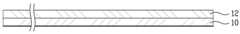
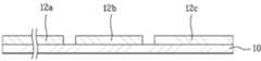
도 1a 내지 도 1g는 종래 복수 개의 단위셀이 직렬로 연결된 구조를 갖는 박막형 태양전지의 제조공정을 도시한 단면도이다.1A to 1G are cross-sectional views illustrating a manufacturing process of a thin film solar cell having a structure in which a plurality of conventional unit cells are connected in series.
우선, 도 1a에서 알 수 있듯이, 기판(10) 상에 ZnO와 같은 투명도전물을 이용하여 전면전극층(12)을 형성한다.First, as shown in FIG. 1A, a
다음, 도 1b에서 알 수 있듯이, 상기 전면전극층(12)을 패터닝하여 단위 전면전극(12a, 12b, 12c)들을 형성한다. 상기 전면전극층(12)의 패터닝 공정은 레이저 스크라이빙(Laser Scribing) 공정을 이용하여 수행한다.Next, as shown in FIG. 1B, the
다음, 도 1c에서 알 수 있듯이, 상기 기판(10) 전면에 반도체층(14)을 형성한다. 상기 반도체층(14)은 실리콘과 같은 반도체물질을 이용하여 형성하는데, P형 반도체층, 진성(Intrinsic) 반도체층 및 N형 반도체층으로 적층된 소위 PIN구조로 형성한다.Next, as shown in FIG. 1C, a
다음, 도 1d에서 알 수 있듯이, 상기 반도체층(14)을 패터닝하여 단위 반도체층(14a, 14b, 14c)을 형성한다. 상기 반도체층(14)의 패터닝 공정은 레이저 스크라이빙공정을 이용하여 수행한다.1D, the
다음, 도 1e에서 알 수 있듯이, 상기 기판(10) 전면에 투명도전층(16) 및 금속층(18)을 차례로 형성하여 후면전극층(20)을 형성한다. 상기 투명도전층(16)으로는 ZnO를 이용하고, 상기 금속층(18)으로는 Al을 이용한다.Next, as shown in FIG. 1E, the transparent
다음, 도 1f에서 알 수 있듯이, 상기 후면전극층(20)을 패터닝하여 단위 후면전극(20a, 20b, 20c)를 형성한다. 여기서, 상기 후면전극층(20)을 패터닝할 때 그 하부의 단위 반도체층(14b, 14c)도 함께 패터닝하며, 이와 같은 패터닝 공정은 레이저 스크라이빙 공정을 이용하여 수행한다.Next, as can be seen in Figure 1f, the
다음, 도 1g에서 알 수 있듯이, 기판(10)의 최외곽 부분에 위치하는 단위 후면전극(20a, 20c), 단위 반도체층(14a, 14c) 및 단위 전면전극(12a, 12c)을 패터닝하여, 기판의 최외곽 부분을 분리한다.Next, as shown in FIG. 1G, the
이와 같이 기판(10)의 최외곽 부분을 패터닝하여 분리하는 이유는, 완성된 박막 태양전지를 모듈화하는 공정에서 소정의 하우징을 박막 태양전지에 연결하게 되는데 이때 상기 하우징과 박막 태양전지 사이에 쇼트가 발생되는 것을 방지하기 위함이다.The reason for separating and patterning the outermost part of the
상기 기판(10)의 최외곽 부분을 패터닝하는 공정은 레이저 스크라이빙 공정을 이용하여 수행하는데, 패터닝하는 최외곽 부분은 복수개의 서로 다른 물질층으로 구성되어 있기 때문에, 상대적으로 작은 파장의 레이저로 단위 후면전극(20a, 20c) 및 단위 반도체층(14a, 14c)을 먼저 스크라이빙하고, 이후에 상대적으로 큰 파장의 레이저로 단위 전면전극(12a, 12c)을 스크라이빙한다.The process of patterning the outermost part of the
그러나, 이와 같은 종래의 박막형 태양전지의 제조방법은 다음과 같은 문제점이 있다.However, such a conventional method of manufacturing a thin film solar cell has the following problems.
첫째, 상기 전면전극층(12)의 패터닝공정(도 1b 참조), 상기 반도체층(14)의 패터닝공정(도 1d 참조), 상기 후면전극층(20)의 패터닝공정(도 1f 참조), 및 상기 기판(10)의 최외곽 부분의 패터닝공정(도 1g 참조)과 같이 총 4차례에 걸친 패터닝공정을 수행해야 하기 때문에 공정이 복잡해지는 문제점이 있다.First, the patterning process of the front electrode layer 12 (see FIG. 1B), the patterning process of the semiconductor layer 14 (see FIG. 1D), the patterning process of the back electrode layer 20 (see FIG. 1F), and the substrate. Since the patterning process of the outermost part of (10) (see FIG. 1G) has to be performed four times in total, there is a problem that the process becomes complicated.
둘째, 총 4차례에 걸친 패터닝 공정을 모두 레이저 스크라이빙 공정을 이용하여 수행하기 때문에 레이저 스크라이빙 공정 중에 발생하는 잔유물이 기판에 잔존하여 기판이 오염될 우려가 커지고, 기판의 오염을 방지하기 위해 세정공정을 추가할 경우 그만큼 공정이 복잡해지고 생산성이 떨어지게 되는 문제점이 있다.Second, since all four patterning processes are performed by using a laser scribing process, residues generated during the laser scribing process may remain on the substrate, thereby increasing the risk of contamination of the substrate and preventing contamination of the substrate. In order to add a cleaning process, there is a problem that the process is complicated and productivity is reduced.
본 발명은 전술한 종래의 박막형 태양전지의 문제점을 해결하기 위해 고안된 것으로서,The present invention has been devised to solve the problems of the conventional thin film type solar cell,
본 발명은 패터닝 공정을 단축하여 보다 간단한 방법으로 박막형 태양전지를 제조할 수 있는 방법 및 그 방법에 의해 제조되는 박막형 태양전지를 제공함을 일 목적으로 한다.An object of the present invention is to provide a method capable of manufacturing a thin film solar cell by a simpler method by shortening the patterning process, and a thin film solar cell manufactured by the method.
본 발명은 패터닝 공정을 수행함에 있어서 레이저 스크라이빙 공정의 이용횟수를 감소시켜 기판의 오염 가능성을 줄이고 그와 더불어 세정공정도 줄여 생산성을 증가시킬 수 있는 박막형 태양전지 제조방법 및 그 방법에 의해 제조되는 박막형 태양전지를 제공함을 다른 목적으로 한다.The present invention reduces the number of times of use of the laser scribing process in performing the patterning process to reduce the possibility of contamination of the substrate and at the same time to reduce the cleaning process and to increase the productivity by manufacturing a thin-film solar cell manufacturing method Another object of the present invention is to provide a thin film solar cell.
본 발명은 상기 목적을 달성하기 위해서, 기판 상에 소정의 간격으로 이격된 복수 개의 단위 전면전극 패턴을 형성하는 제1공정; 상기 기판 상에서, 단위셀로 나누기 위한 분리부 및 전극간 연결을 위한 콘택부를 구비한 반도체층 패턴을 형성하는 제2공정; 및 상기 콘택부를 통해 상기 단위 전면전극 패턴과 연결되며, 상기 분리부에 의해 이격되는 복수 개의 단위 후면전극 패턴을 형성하는 제3공정을 포함하여 이루어진 박막형 태양전지 제조방법을 제공한다.The present invention to achieve the above object, the first step of forming a plurality of unit front electrode patterns spaced at a predetermined interval on the substrate; Forming a semiconductor layer pattern on the substrate, the semiconductor layer pattern having a separation part for dividing into unit cells and a contact part for connection between electrodes; And a third process of connecting the unit front electrode pattern through the contact unit to form a plurality of unit back electrode patterns spaced apart from the separation unit.
상기 제1공정은 상기 복수 개의 단위 전면전극 패턴 중 최외곽의 단위 전면전극 패턴에 제1격리부를 형성하여, 상기 제1격리부에 의해 기판의 최외곽부분을 격리시키는 공정을 포함할 수 있다.The first process may include forming a first isolation portion on the outermost unit front electrode pattern among the plurality of unit front electrode patterns to isolate the outermost portion of the substrate by the first isolation portion.
상기 제1공정은 상기 기판 상에 전면전극층을 형성하는 공정, 및 상기 전면전극층을 패터닝하는 공정으로 이루어질 수 있다.The first process may include forming a front electrode layer on the substrate, and patterning the front electrode layer.
상기 제1공정은 스크린인쇄법, 잉크젯인쇄법, 그라비아인쇄법 또는 미세접촉인쇄법을 이용하여 상기 기판 상에 전면전극 패턴을 형성하는 공정으로 이루어질 수 있다.The first process may be performed by forming a front electrode pattern on the substrate by using a screen printing method, an inkjet printing method, a gravure printing method, or a microcontact printing method.
상기 제1공정은 상기 전면전극 패턴의 표면에 대한 텍스처 가공공정을 추가로 포함할 수 있다.The first process may further include a texture processing process for the surface of the front electrode pattern.
상기 제2공정은 상기 기판 전면에 반도체층을 형성하는 공정, 및 상기 반도체층을 패터닝하는 공정으로 이루어질 수 있다.The second process may include a process of forming a semiconductor layer on the entire surface of the substrate, and a process of patterning the semiconductor layer.
상기 제2공정은 상기 기판 전면에 반도체층과 투명도전층을 차례로 형성하는 공정, 및 상기 반도체층과 투명도전층을 패터닝하는 공정으로 이루어질 수 있다.The second process may include a process of sequentially forming a semiconductor layer and a transparent conductive layer on the entire surface of the substrate, and a process of patterning the semiconductor layer and the transparent conductive layer.
상기 제2공정은 상기 반도체층 패턴 중 최외곽의 반도체층 패턴에 상기 전면전극 패턴의 제1격리부에 대응하는 제2격리부를 형성하여, 상기 제1격리부와 제2격리부에 의해 기판의 최외곽부분을 격리시키는 공정을 포함할 수 있다.In the second process, a second isolation portion corresponding to the first isolation portion of the front electrode pattern is formed on the outermost semiconductor layer pattern among the semiconductor layer patterns, and the first isolation portion and the second isolation portion are used to form a substrate. It may include a process to isolate the outermost part.
상기 제2공정은 P형 반도체층, 진성(Intrinsic) 반도체층 및 N형 반도체층이 순서대로 적층된 PIN구조의 반도체층 패턴을 형성하는 공정으로 이루어질 수 있다.The second process may include a process of forming a semiconductor layer pattern having a PIN structure in which a P-type semiconductor layer, an intrinsic semiconductor layer, and an N-type semiconductor layer are sequentially stacked.
상기 제3공정은 스크린인쇄법, 잉크젯인쇄법, 그라비아인쇄법 또는 미세접촉인쇄법을 이용하여 후면전극 패턴을 형성하는 공정으로 이루어질 수 있다.The third process may be performed by forming a back electrode pattern by using a screen printing method, an inkjet printing method, a gravure printing method, or a microcontact printing method.
상기 제3공정은 상기 후면전극 패턴 중 최외곽의 후면전극 패턴에 상기 전면 전극 패턴의 제1격리부에 대응하는 제3격리부를 형성하여, 상기 제1격리부, 제2격리부 및 제3격리부에 의해 기판의 최외곽부분을 격리시키는 공정을 포함할 수 있다.In the third process, a third isolation portion corresponding to the first isolation portion of the front electrode pattern is formed on the outermost rear electrode pattern among the rear electrode patterns, and the first isolation portion, the second isolation portion, and the third isolation portion are formed. It may include a step of isolating the outermost portion of the substrate by the portion.
본 발명은 상기 목적을 달성하기 위해서, 기판 상에 전면전극층을 형성하는 공정; 상기 전면전극층을 패터닝하여, 최외곽에 제1격리부를 구비하며 소정의 간격으로 이격된 복수 개의 단위 전면전극 패턴을 형성하는 공정; 상기 기판 전면에 반도체층과 투명도전층을 차례로 형성하는 공정; 상기 반도체층과 투명도전층을 패터닝하여, 단위셀로 나누기 위한 분리부, 전극간 연결을 위한 콘택부, 및 상기 전면전극 패턴의 제1격리부에 대응하는 제2격리부를 형성하는 공정; 및 상기 전면전극 패턴의 제1격리부에 대응하는 제3격리부를 구비하고, 상기 콘택부를 통해 상기 단위 전면전극 패턴과 연결되고 상기 분리부에 의해 이격되는 복수 개의 단위 후면전극 패턴을 형성하는 공정을 포함하는 박막형 태양전지 제조방법을 제공한다.The present invention to achieve the above object, the step of forming a front electrode layer on a substrate; Patterning the front electrode layer to form a plurality of unit front electrode patterns spaced at predetermined intervals with a first isolation portion at an outermost portion thereof; Sequentially forming a semiconductor layer and a transparent conductive layer on the entire surface of the substrate; Patterning the semiconductor layer and the transparent conductive layer to form a separation part for dividing into unit cells, a contact part for inter-electrode connection, and a second isolation part corresponding to the first isolation part of the front electrode pattern; And a third isolation portion corresponding to the first isolation portion of the front electrode pattern, and forming a plurality of unit rear electrode patterns connected to the unit front electrode pattern through the contact portion and spaced apart by the separation portion. It provides a thin-film solar cell manufacturing method comprising the.
상기 단위 후면 전극 패턴을 형성하는 공정은 스크린인쇄법, 잉크젯인쇄법, 그라비아인쇄법 또는 미세접촉인쇄법을 이용하여 수행할 수 있다.The process of forming the unit back electrode pattern may be performed by using a screen printing method, an inkjet printing method, a gravure printing method, or a microcontact printing method.
본 발명은 상기 목적을 달성하기 위해서, 기판 상에 소정의 간격으로 이격된 복수 개의 단위 전면전극 패턴; 상기 기판 상에서, 단위셀로 나누기 위한 분리부 및 전극간 연결을 위한 콘택부를 구비한 반도체층 패턴; 상기 반도체층 패턴 상부에서, 상기 반도체층 패턴과 동일한 패턴으로 형성된 투명도전층 패턴; 및 상기 콘택부를 통해 상기 단위 전면전극 패턴과 연결되며, 상기 분리부에 의해 이격되는 복수 개의 단위 후면전극 패턴을 포함하여 이루어진 박막형 태양전지를 제공한다.The present invention provides a plurality of unit front electrode patterns spaced at predetermined intervals on the substrate to achieve the above object; A semiconductor layer pattern having a separating part for dividing into unit cells and a contact part for connecting between electrodes on the substrate; A transparent conductive layer pattern formed on the semiconductor layer pattern in the same pattern as the semiconductor layer pattern; And a plurality of unit back electrode patterns connected to the unit front electrode pattern through the contact unit and spaced apart from the separation unit.
상기 복수 개의 단위 전면전극 패턴 중 최외곽의 단위 전면전극 패턴에 제1격리부가 구비될 수 있다.A first isolation part may be provided on the outermost unit front electrode pattern among the plurality of unit front electrode patterns.
상기 반도체층 패턴은 상기 전면전극 패턴의 제1격리부에 대응하는 부분에 반도체층이 형성되지 않은 제2격리부를 구비하고, 상기 후면전극 패턴은 상기 전면전극 패턴의 제1격리부에 대응하는 부분에 후면전극이 형성되지 않은 제3격리부를 구비할 수 있다.The semiconductor layer pattern may include a second isolation portion in which a semiconductor layer is not formed on a portion corresponding to the first isolation portion of the front electrode pattern, and the rear electrode pattern may correspond to a first isolation portion of the front electrode pattern. It may be provided with a third isolating portion is not formed on the back electrode.
상기 복수 개의 단위 전면전극 패턴은 그 표면이 요철구조로 이루어질 수 있다.The surface of the plurality of unit front electrode patterns may have an uneven structure.
상기 반도체층 패턴은 P형 반도체층, 진성(Intrinsic) 반도체층 및 N형 반도체층이 순서대로 적층된 PIN구조로 이루어질 수 있다.The semiconductor layer pattern may have a PIN structure in which a P-type semiconductor layer, an intrinsic semiconductor layer, and an N-type semiconductor layer are sequentially stacked.
상기와 같은 본 발명에 따르면 다음과 같은 효과가 있다.According to the present invention as described above, the following effects can be obtained.
첫째, 본 발명은 단위 전면전극의 패턴형성공정, 반도체층의 패턴형성공정, 및 단위 후면전극의 패턴형성공정과 같은 총 3차례의 패턴형성공정을 통해 박막형 태양전지를 제조하기 때문에 종래에 비하여 패턴형성공정이 감소되어 전체적으로 공정이 단순화되는 효과가 있다.First, since the present invention manufactures a thin-film solar cell through a total of three pattern forming processes such as a pattern forming process of a unit front electrode, a pattern forming process of a semiconductor layer, and a pattern forming process of a unit back electrode, a pattern is compared with the conventional art. The forming process is reduced, thereby reducing the overall process.
특히, 종래에는 기판의 최외곽부분을 패터닝하기 위한 공정을 별도로 수행하였지만, 본 발명은 3차례의 패턴형성공정에서 기판의 최외곽부분에 대한 패터닝을 병행하기 때문에, 즉, 3차례의 패턴형성공정 중에 각각 제1격리부, 제2격리부, 및 제3격리부를 형성하기 때문에, 기판의 최외곽부분에 대한 패터닝을 위한 별도의 공 정이 필요하지 않게 된다.In particular, in the prior art, the process for patterning the outermost part of the substrate was separately performed. However, since the present invention performs patterning on the outermost part of the substrate in three pattern forming processes, that is, three pattern forming processes. Since the first isolating portion, the second isolating portion, and the third isolating portion are formed respectively, no separate process for patterning the outermost portion of the substrate is required.
둘째, 본 발명은 총 3차례의 패턴형성공정을 수행함에 있어서 레이저 스크라이빙공정을 최소화함으로써, 레이저 스크라이빙공정에 의해 발생하는 기판의 오염문제 및 세정공정 추가로 인한 생산성 감소 문제가 줄어드는 효과가 있다.Second, the present invention minimizes the laser scribing process in performing the pattern formation process three times, thereby reducing the problem of substrate contamination caused by the laser scribing process and the productivity reduction problem due to the addition of the cleaning process. There is.
즉, 본 발명에서는 단위 후면전극의 패턴형성공정을 수행함에 있어서 레이저 스크라이빙공정 대신에 스크린 인쇄법, 잉크젯 인쇄법, 그라비아 인쇄법 또는 미세접촉 인쇄법을 이용하기 때문에 그만큼 레이저 스크라이빙 공정 회수가 감소되는 효과가 있다. 또한, 단위 후면전극의 패턴형성공정과 더불어 단위 전면전극의 패턴형성공정에도 상기 스크린 인쇄법, 잉크젯 인쇄법, 그라비아 인쇄법 또는 미세접촉 인쇄법을 이용할 경우 레이저 스크라이빙 공정 회수가 2회 감소되는 효과가 있다.That is, in the present invention, since the screen forming method, the inkjet printing method, the gravure printing method, or the microcontact printing method is used instead of the laser scribing process in performing the pattern forming process of the unit back electrode, the number of laser scribing processes is increased accordingly. Has the effect of decreasing. In addition, the screen forming method, the inkjet printing method, the gravure printing method, or the microcontact printing method can reduce the number of laser scribing processes twice in addition to the pattern forming process of the unit back electrode. It works.
이하, 도면을 참조로 본 발명의 바람직한 실시예에 대해서 상세히 설명하기로 한다.Hereinafter, preferred embodiments of the present invention will be described in detail with reference to the drawings.
<박막형 태양전지 제조방법><Thin Film Solar Cell Manufacturing Method>
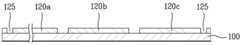
도 2a 내지 도 2f는 본 발명의 일 실시예에 따른 박막형 태양 전지의 제조공정을 도시한 단면도이다.2A to 2F are cross-sectional views illustrating a manufacturing process of a thin film solar cell according to an embodiment of the present invention.
우선, 도 2a에서 알 수 있듯이, 기판(100) 상에 전면전극층(120)을 형성한다.First, as shown in FIG. 2A, the
상기 기판(100)으로는 유리 또는 투명한 플라스틱을 이용할 수 있다.Glass or transparent plastic may be used as the
상기 전면전극층(120)은 ZnO, ZnO:B, ZnO:Al, SnO2, SnO2:F, ITO(Indium Tin Oxide), 등과 같은 투명한 도전물질을 스퍼터링(Sputtering)법 또는 MOCVD(Metal Organic Chemical Vapor Deposition)법 등을 이용하여 형성할 수 있다.The
상기 전면전극층(120)은 태양광이 입사되는 면이기 때문에 입사되는 태양광이 태양전지 내부로 최대한 흡수될 수 있도록 하는 것이 중요하며, 이를 위해서 상기 전면전극층(120)에 텍스처(texturing) 가공공정을 추가로 수행할 수 있다.Since the
상기 텍스처 가공공정이란 물질 표면을 울퉁불퉁한 요철구조로 형성하여 마치 직물의 표면과 같은 형상으로 가공하는 공정으로서, 포토리소그라피법(photolithography)을 이용한 식각공정, 화학용액을 이용한 이방성 식각공정(anisotropic etching), 또는 기계적 스크라이빙(mechanical scribing)을 이용한 홈 형성 공정 등을 통해 수행할 수 있다. 이와 같은 텍스처 가공공정을 상기 전면전극층(120)에 수행할 경우 입사되는 태양광이 태양전지 외부로 반사되는 비율은 감소하게 되며, 그와 더불어 입사되는 태양광의 산란에 의해 태양전지 내부로 태양광이 흡수되는 비율은 증가하게 되어, 태양전지의 효율이 증진되는 효과가 있다.The texturing process is a process in which the material surface is formed into a rugged concavo-convex structure so as to be processed into the same shape as the surface of the fabric. An etching process using photolithography, anisotropic etching using a chemical solution, , Or a groove forming process using mechanical scribing, or the like. When the texture processing process is performed on the
다음, 도 2b에서 알 수 있듯이, 상기 전면전극층(120)을 패터닝한다.Next, as can be seen in Figure 2b, the
상기 전면전극층(120)의 패터닝 공정을 통해서, 소정의 간격으로 이격된 복수개의 단위 전면전극 패턴(120a, 120b, 120c)을 형성하고, 또한 최외곽의 단위 전면 전극 패턴(120a, 120c)에 제1격리부(125)를 형성한다. 상기 제1격리부(125)는 완성된 박막 태양전지를 모듈화하는 공정에서 소정의 하우징을 박막 태양전지에 연 결하게 될 때 상기 하우징과 박막 태양전지 사이에 쇼트가 발생되는 것을 방지하기 위한 것으로서, 상기 제1격리부(120)에 의해 기판(100)의 최외곽부분이 격리된다.Through the patterning process of the
상기 전면전극층(120)의 패터닝 공정은 레이저 스크라이빙법을 이용하여 수행할 수 있다.The patterning process of the
한편, 도 2a 및 도 2b와 같이 기판(100) 전면에 전면전극층(120)을 형성하고 레이저 스크라이빙법을 이용하여 단위 전면전극 패턴(120a, 120b, 120c)을 형성하는 대신에, 스크린 인쇄법(screen printing), 잉크젯 인쇄법(inkjet printing), 그라비아 인쇄법(gravure printing) 또는 미세접촉 인쇄법(microcontact printing)과 같은 보다 간편한 방법을 이용하여 단위 전면전극 패턴(120a, 120b, 120c)을 직접 형성하는 것도 가능하다.2A and 2B, instead of forming the
상기 스크린 인쇄법은 스크린과 스퀴즈(squeeze)를 이용하여 대상물질을 작업물에 전이시켜 소정의 패턴을 형성하는 방법이고, 상기 잉크젯 인쇄법은 잉크젯을 이용하여 대상물질을 작업물에 분사하여 소정의 패턴을 형성하는 방법이고, 상기 그라비아 인쇄법은 오목판의 홈에 대상물질을 도포하고 그 대상물질을 다시 작업물에 전이시켜 소정의 패턴을 형성하는 방법이고, 상기 미세접촉 인쇄법은 소정의 금형을 이용하여 작업물에 대상물질 패턴을 형성하는 방법이다.The screen printing method is a method of forming a predetermined pattern by transferring a target material to a work using a screen and a squeeze. In the inkjet printing method, an object is sprayed onto a work using an inkjet, The gravure printing method is a method of applying a target material to a groove of a concave plate and transferring the target material to a workpiece again to form a predetermined pattern. The fine contact printing method is a method of forming a predetermined mold To form a target material pattern on a workpiece.
이와 같이, 스크린 인쇄법, 잉크젯 인쇄법, 그라비아 인쇄법 또는 미세접촉 인쇄법을 이용하여 단위 전면전극 패턴(120a, 120b, 120c)을 형성할 경우 레이저 스크라이빙법을 이용하는 경우에 비하여 기판이 오염될 우려가 줄어들고 기판의 오염 방지를 위한 세정공정 또한 줄어들게 된다.As such, when the unit
또한, 기판(100) 전면에 전면전극층(120)을 형성하고 포토리소그라피법을 이용하여 단위 전면전극 패턴(120a, 120b, 120c)을 형성하는 것도 가능하다.In addition, the
다음, 도 2c에서 알 수 있듯이, 상기 기판(100) 전면에 반도체층(140)을 형성한다. 상기 반도체층(140)은 도시된 바와 같이, 이격된 단위 전면 전극 패턴(120a, 120b, 120c)들 사이의 공간, 상기 격리부(125) 내부, 및 상기 단위 전면 전극 패턴(120a, 120b, 120c) 상부에 형성되게 된다.Next, as shown in FIG. 2C, the
상기 반도체층(140)은 실리콘계, CuInSe2계, CdTe계 등의 반도체물질을 플라즈마 CVD법 등을 이용하여 형성할 수 있으며, 상기 실리콘계 반도체물질로는 비정질 실리콘(a-Si:H) 또는 미세결정 실리콘(μc-Si:H)을 이용할 수 있다.The
상기 반도체층(140)은 P형 반도체층, 진성(Intrinsic) 반도체층 및 N형 반도체층이 순서대로 적층된 PIN구조로 형성할 수 있다. 상기 반도체층(140)은 태양광에 의해 정공(hole) 및 전자(electron)를 생성하고 생성된 정공 및 전자가 각각 P형 반도체층 및 N형 반도체층에서 수집되는데, 이와 같은 정공 및 전자의 수집효율을 증진시키기 위해서는 P형 반도체층과 N형 반도체층만으로 이루어진 PN구조에 비하여 PIN구조가 보다 바람직하다.The
이와 같이 상기 반도체층(140)을 PIN구조로 형성하게 되면, 진성 반도체층이 P형 반도체층과 N형 반도체층에 의해 공핍(depletion)이 되어 내부에 전기장이 발생하게 되고, 태양광에 의해 생성되는 정공 및 전자가 상기 전기장에 의해 드리프트(drift)되어 각각 P형 반도체층 및 N형 반도체층에서 수집되게 된다.When the
한편, 상기 반도체층(140)을 PIN구조로 형성할 경우에는 상기 단위 전면전극 패턴(120a, 120b, 120c) 상부에 P형 반도체층을 형성하고 이어서 진성(Intrinsic) 반도체층 및 N형 반도체층을 형성하는 것이 바람직하다. 그 이유는 일반적으로 정공의 드리프트 이동도(drift mobility)가 전자의 드리프트 이동도에 의해 낮기 때문에 입사광에 의한 수집효율을 극대화하기 위해서 P형 반도체층을 수광면에 가깝게 형성하기 위함이다.In the case where the
다음, 도 2d에서 알 수 있듯이, 상기 반도체층(140) 위에 투명도전층(160)을 형성한다.Next, as shown in FIG. 2D, the transparent
상기 투명도전층(160)은 ZnO, ZnO:B, ZnO:Al, Ag와 같은 투명한 도전물질을 스퍼터링(Sputtering)법 또는 MOCVD(Metal Organic Chemical Vapor Deposition)법 등을 이용하여 형성할 수 있다.The transparent
상기 투명도전층(160)의 형성공정은 생략하는 것도 가능하지만, 태양전지의 효율증진을 위해서는 상기 투명도전층(160)을 형성하는 것이 바람직하다. 즉, 상기 투명도전층(160)을 형성하게 되면 상기 반도체층(140)을 투과한 태양광이 투명도전층(160)을 통과하면서 산란을 통해 다양한 각으로 진행하게 되어 후술하는 후면전극 패턴(180a, 180b, 180c)(도 2f 공정 참조)에서 반사되어 상기 반도체층(140)으로 재입사되는 광의 비율이 증가될 수 있기 때문이다.Although the formation process of the transparent
다음, 도 2e에서 알 수 있듯이, 상기 반도체층(140) 및 투명도전층(160)을 동시에 패터닝하여, 반도체층 패턴(140a) 및 투명도전층 패턴(160a)을 형성한다.Next, as shown in FIG. 2E, the
상기 반도체층(140) 및 투명도전층(160)의 패터닝 공정에 의해 분리부(170), 콘택부(172), 및 제2격리부(174)를 형성한다.The
상기 분리부(170)은 태양전지를 단위셀로 나누기 위한 것이고, 상기 콘택부(172)는 전술한 단위 전면전극 패턴(120b, 120c)과 후술할 단위 후면전극 패턴(180a, 180b)(도 2f 공정 참조) 간의 전기적 연결을 위한 것이다. 상기 제2격리부(174)는 전술한 전면전극의 제1격리부(125)에 대응하며, 상기 반도체층(140) 및 투명도전층(160)의 최외곽 부분을 제거함으로써 형성한다. 따라서, 상기 제1격리부(125) 및 제2격리부(174)에 의해 기판의 최외곽 부분이 격리되게 된다.The
상기 반도체층(140)과 투명도전층(160)의 패터닝 공정은 레이저 스크라이빙 공정을 통해 수행할 수도 있으나, 반드시 그에 한정되는 것은 아니고, 포토리소그라피 공정을 이용하여 수행하는 것도 가능하다.The patterning process of the
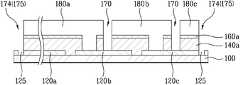
다음, 도 2f에서 알 수 있듯이, 상기 분리부(170)를 사이에 두고 이격되는 복수 개의 단위 후면전극 패턴(180a, 180b, 180c)을 형성한다.Next, as shown in FIG. 2F, a plurality of unit back
상기 복수 개의 단위 후면전극 패턴(180a, 180b)은 전술한 콘택부(172)를 통해 전술한 단위 전면전극 패턴(120b, 120c)과 각각 연결된다. 또한, 최외곽의 단위 후면 전극 패턴(180a, 180c)에는 전술한 전면전극의 제1격리부(125)에 대응하며, 상기 제2격리부(174)와 동일한 위치에 제3격리부(175)가 형성된다. 따라서, 상기 제1격리부(125), 제2격리부(174), 및 제3격리부(175)에 의해 기판의 최외곽 부분이 격리되게 된다.The plurality of unit back
이와 같이, 단위 전면전극(120a, 120c)의 제1격리부(125), 반도체층(140)과 투명도전층(160)의 제2격리부(174), 및 단위 후면전극(180a, 180c)의 제3격리 부(175)에 의해 박막 태양전지의 최외곽부분이 분리되어 모듈공정시 하우징과 박막 태양전지 사이에 쇼트가 발생하는 것이 방지되게 된다. 특히, 상기 제1격리부(125), 제2격리부(174) 및 제3격리부(175)를 전면전극층(120), 반도체층(140), 투명도전층(160) 및 후면전극층(180)의 패터닝 공정시 병행하여 형성하기 때문에 박막 태양전지의 최외곽부분의 분리를 위한 별도의 공정이 요하지 않게 된다.As such, the
상기 단위 후면전극 패턴(180a, 180b, 180c)은 스크린인쇄법(screen printing), 잉크젯인쇄법(inkjet printing), 그라비아인쇄법(gravure printing) 또는 미세접촉인쇄법(microcontact printing)을 이용하여 수행하며, 그 재료로는 Ag, Al, Ag+Mo, Ag+Ni, Ag+Cu 등과 같은 금속을 이용한다.The unit back
<박막형 태양전지><Thin-film solar cell>
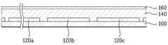
도 3은 본 발명의 일 실시예에 따른 박막형 태양전지의 단면도이다.3 is a cross-sectional view of a thin film solar cell according to an embodiment of the present invention.
도 3에서 알 수 있듯이, 본 발명의 일 실시예에 따른 박막형 태양전지는 기판(100), 복수 개의 단위 전면전극 패턴(120a, 120b, 120c), 반도체층 패턴(140a), 투명도전층 패턴(160a), 및 복수 개의 단위 후면전극 패턴(180a, 180b, 180c)을 포함하여 이루어진다.As can be seen in Figure 3, the thin-film solar cell according to an embodiment of the present invention is a
상기 기판(100)은 유리 또는 투명한 플라스틱으로 이루어질 수 있다.The
상기 복수 개의 단위 전면전극 패턴(120a, 120b, 120c)은 ZnO, ZnO:B, ZnO:Al, SnO2, SnO2:F, 또는 ITO(Indium Tin Oxide)등과 같은 투명한 도전물질로 이루어질 수 있다.The plurality of unit
상기 복수 개의 단위 전면전극 패턴(120a, 120b, 120c)은 상기 기판(100) 상에서 소정의 간격으로 이격되어 형성되며, 상기 복수 개의 단위 전면전극 패턴 중 최외곽의 단위 전면전극 패턴(120a, 120c)에는 제1격리부(125)가 구비되어 있다.The plurality of unit
상기 복수 개의 단위 전면전극 패턴(120a, 120b, 120c)은 텍스처 가공공정 등을 통해 그 표면이 울퉁불퉁한 요철구조로 형성될 수 있다.The plurality of unit
상기 반도체층 패턴(140a)은 실리콘계, CuInSe2계, CdTe계 등의 반도체물질로 이루어지며, P형 반도체층, 진성(Intrinsic) 반도체층 및 N형 반도체층이 순서대로 적층된 PIN구조로 이루어질 수 있다.The
상기 반도체층 패턴(140a)은 단위셀로 나누기 위한 분리부(170) 및 전극간 연결을 위한 콘택부(172)을 구비하며, 상기 반도체층 패턴(140a)의 최외곽 부분에는 상기 단위 전면전극 패턴(120a, 120c)의 제1격리부(125)에 대응하도록 제2격리부(174)가 형성된다.The
상기 투명도전층 패턴(160a)은 ZnO, ZnO:B, ZnO:Al, Ag와 같은 투명한 도전물질로 이루어질 수 있다.The transparent
상기 투명도전층 패턴(160a)은 상기 반도체층 패턴(140a) 상부에서 상기 반도체층 패턴(140a)과 동일한 패턴으로 형성된다. 즉, 상기 투명도전층 패턴(160a)은 분리부(170) 및 콘택부(172)을 구비하며, 그 최외곽 부분에는 제2격리부(174)가 형성된다.The transparent
상기 복수 개의 단위 후면전극 패턴(180a, 180b, 180c)은 상기 분리부(170) 에 의해 서로 이격되어 있으며, 상기 복수 개의 단위 후면전극 패턴(180a, 180b)은 상기 콘택부(172)를 통해 상기 단위 전면전극 패턴(120b, 120c)과 각각 연결되어 있다. 또한, 최외곽의 단위 후면 전극 패턴(180a, 180c)에는 상기 전면전극의 제1격리부(125)에 대응하는 제3격리부(175)가 형성되어 있다. 상기 제3격리부(175)는 전술한 제2격리부(174)와 동일한 위치에 형성된다.The plurality of unit back
이와 같은 본 발명의 일 실시예에 따른 박막형 태양 전지는 전술한 도 2a 내지 도 2f에 따른 방법에 의해 제조될 수 있다.Such a thin film solar cell according to an embodiment of the present invention may be manufactured by the method according to FIGS. 2A to 2F described above.
도 1a 내지 도 1g는 종래 복수 개의 단위셀이 직렬로 연결된 구조를 갖는 박막형 태양전지의 제조공정을 도시한 단면도이다.1A to 1G are cross-sectional views illustrating a manufacturing process of a thin film solar cell having a structure in which a plurality of conventional unit cells are connected in series.
도 2a 내지 도 2f는 본 발명의 일 실시예에 따른 박막형 태양 전지의 제조공정을 도시한 단면도이다.2A to 2F are cross-sectional views illustrating a manufacturing process of a thin film solar cell according to an embodiment of the present invention.
도 3은 본 발명의 일 실시예에 따른 박막형 태양 전지를 도시한 단면도이다.3 is a cross-sectional view showing a thin film solar cell according to an embodiment of the present invention.
<도면의 주요부의 부호에 대한 설명>DESCRIPTION OF THE REFERENCE NUMERALS OF THE DRAWINGS FIG.
100: 기판 120: 전면전극층100: substrate 120: front electrode layer
120a, 120b, 120c: 단위 전면전극 패턴 125: 제1격리부120a, 120b, and 120c: unit front electrode pattern 125: first isolation unit
140: 반도체층 140a: 반도체층 패턴140:
160: 투명도전층 160a: 투명도전층 패턴160: transparent
170: 분리부 172: 콘택부170: separating portion 172: contact portion
174: 제2격리부 175: 제3격리부174: second containment 175: third containment
180a, 180b, 180c: 단위 후면전극 패턴180a, 180b, 180c: unit back electrode pattern
Claims (17)
Translated fromKoreanPriority Applications (6)
| Application Number | Priority Date | Filing Date | Title |
|---|---|---|---|
| KR1020070078405AKR101301664B1 (en) | 2007-08-06 | 2007-08-06 | The method for manufacturing Thin film type Solar Cell, and Thin film type Solar Cell made by the method |
| TW097129937ATWI464898B (en) | 2007-08-06 | 2008-08-06 | Thin film type solar cell and manufacturing method thereof |
| PCT/KR2008/004573WO2009020349A2 (en) | 2007-08-06 | 2008-08-06 | Method for manufacturing thin film type solar cell, and thin film type solar cell made by the method |
| CN201110236582XACN102299199A (en) | 2007-08-06 | 2008-08-06 | Method for manufacturing thin film type solar cell, and thin film type solar cell made by the method |
| US12/672,494US20110162684A1 (en) | 2007-08-06 | 2008-08-06 | Method for manufacturing thin film type solar cell, and thin film type solar cell made by the method |
| CN2008801016654ACN101772843B (en) | 2007-08-06 | 2008-08-06 | Method for manufacturing thin-film solar cell and thin-film solar cell manufactured by the method |
Applications Claiming Priority (1)
| Application Number | Priority Date | Filing Date | Title |
|---|---|---|---|
| KR1020070078405AKR101301664B1 (en) | 2007-08-06 | 2007-08-06 | The method for manufacturing Thin film type Solar Cell, and Thin film type Solar Cell made by the method |
Publications (2)
| Publication Number | Publication Date |
|---|---|
| KR20090014450A KR20090014450A (en) | 2009-02-11 |
| KR101301664B1true KR101301664B1 (en) | 2013-08-29 |
Family
ID=40341906
Family Applications (1)
| Application Number | Title | Priority Date | Filing Date |
|---|---|---|---|
| KR1020070078405AActiveKR101301664B1 (en) | 2007-08-06 | 2007-08-06 | The method for manufacturing Thin film type Solar Cell, and Thin film type Solar Cell made by the method |
Country Status (5)
| Country | Link |
|---|---|
| US (1) | US20110162684A1 (en) |
| KR (1) | KR101301664B1 (en) |
| CN (2) | CN102299199A (en) |
| TW (1) | TWI464898B (en) |
| WO (1) | WO2009020349A2 (en) |
Families Citing this family (17)
| Publication number | Priority date | Publication date | Assignee | Title |
|---|---|---|---|---|
| EP2214462B1 (en) | 2009-01-30 | 2012-09-19 | SANYO Electric Co., Ltd. | Display apparatus and display system |
| TWI426551B (en)* | 2009-03-25 | 2014-02-11 | Ind Tech Res Inst | Three-dimensional metal oxide electrodes and fabrication method thereof |
| WO2010123196A1 (en)* | 2009-04-24 | 2010-10-28 | Jusung Engineering Co., Ltd. | Thin film type solar cell, and method for manufacturing the same |
| KR101053782B1 (en)* | 2009-06-23 | 2011-08-03 | 주성엔지니어링(주) | Thin film type solar cell and manufacturing method thereof |
| US8129658B2 (en)* | 2009-08-06 | 2012-03-06 | Applied Materials, Inc. | Systems for thin film laser scribing devices |
| US8890025B2 (en)* | 2009-09-24 | 2014-11-18 | Esi-Pyrophotonics Lasers Inc. | Method and apparatus to scribe thin film layers of cadmium telluride solar cells |
| KR20120098623A (en)* | 2009-09-24 | 2012-09-05 | 이에스아이-파이로포토닉스 레이저스, 인코포레이티드 | Method and apparatus to scribe a line in a thin film material using a burst of laser pulses with beneficial pulse shape |
| DE102009044142A1 (en)* | 2009-09-30 | 2011-03-31 | Saint-Gobain Sekurit Deutschland Gmbh & Co. Kg | Thin-film component on glass, a process for its production and its use |
| KR101295547B1 (en)* | 2009-10-07 | 2013-08-12 | 엘지전자 주식회사 | Thin film type solar cell module and manufacturing method thereof |
| KR101641929B1 (en)* | 2010-03-08 | 2016-07-25 | 주성엔지니어링(주) | Sola Cell of Thin Film and Method for Fabricating the same |
| KR20110137671A (en) | 2010-06-17 | 2011-12-23 | 엘지디스플레이 주식회사 | Manufacturing Method of Thin Film Solar Cell |
| US8563351B2 (en)* | 2010-06-25 | 2013-10-22 | Taiwan Semiconductor Manufacturing Co., Ltd. | Method for manufacturing photovoltaic device |
| JP2012064933A (en)* | 2010-08-19 | 2012-03-29 | Semiconductor Energy Lab Co Ltd | Photoelectric conversion module and its manufacturing method |
| KR101172186B1 (en)* | 2010-10-05 | 2012-08-07 | 엘지이노텍 주식회사 | Solar cell apparatus and method of fabricating the same |
| WO2012106360A1 (en)* | 2011-02-01 | 2012-08-09 | EncoreSolar, Inc. | Monolithic integration of super-strate thin film photovoltaic modules |
| KR101283302B1 (en)* | 2011-04-04 | 2013-07-11 | 엘지이노텍 주식회사 | Solar cell apparatus and method of fabricating the same |
| US9555502B2 (en) | 2012-07-27 | 2017-01-31 | First Solar, Inc. | Dual lasers for removing glass-side debris during the manufacture of thin film photovoltaic devices |
Citations (1)
| Publication number | Priority date | Publication date | Assignee | Title |
|---|---|---|---|---|
| KR101188122B1 (en) | 2011-08-10 | 2012-10-09 | 주식회사 아바코 | Monolithically connected thin film type solar cell and method for manufacturing the same |
Family Cites Families (9)
| Publication number | Priority date | Publication date | Assignee | Title |
|---|---|---|---|---|
| US4732621A (en)* | 1985-06-17 | 1988-03-22 | Sanyo Electric Co., Ltd. | Method for producing a transparent conductive oxide layer and a photovoltaic device including such a layer |
| JPH06104465A (en)* | 1992-09-22 | 1994-04-15 | Fuji Electric Co Ltd | Thin film solar cell and method of manufacturing the same |
| EP0931356B1 (en)* | 1996-09-26 | 2004-08-18 | Akzo Nobel N.V. | A photovoltaic foil and method of manufacturing it |
| EP1089346B1 (en)* | 1999-09-28 | 2011-03-02 | Kaneka Corporation | Method of controlling manufacturing process of photoelectric conversion apparatus |
| AU7684001A (en)* | 2000-07-06 | 2002-01-21 | Bp Corp North America Inc | Partially transparent photovoltaic modules |
| JP4987191B2 (en)* | 2001-03-21 | 2012-07-25 | 株式会社カネカ | Method for manufacturing integrated thin film solar cell |
| JP2003273383A (en)* | 2002-03-15 | 2003-09-26 | Sharp Corp | Solar cell element and manufacturing method therefor |
| JP4064340B2 (en)* | 2003-12-25 | 2008-03-19 | 昭和シェル石油株式会社 | Manufacturing method of integrated thin film solar cell |
| JP2006332453A (en)* | 2005-05-27 | 2006-12-07 | Sharp Corp | Thin film solar cell manufacturing method and thin film solar cell |
- 2007
- 2007-08-06KRKR1020070078405Apatent/KR101301664B1/enactiveActive
- 2008
- 2008-08-06WOPCT/KR2008/004573patent/WO2009020349A2/enactiveApplication Filing
- 2008-08-06CNCN201110236582XApatent/CN102299199A/enactivePending
- 2008-08-06CNCN2008801016654Apatent/CN101772843B/ennot_activeExpired - Fee Related
- 2008-08-06USUS12/672,494patent/US20110162684A1/ennot_activeAbandoned
- 2008-08-06TWTW097129937Apatent/TWI464898B/enactive
Patent Citations (1)
| Publication number | Priority date | Publication date | Assignee | Title |
|---|---|---|---|---|
| KR101188122B1 (en) | 2011-08-10 | 2012-10-09 | 주식회사 아바코 | Monolithically connected thin film type solar cell and method for manufacturing the same |
Also Published As
| Publication number | Publication date |
|---|---|
| CN101772843A (en) | 2010-07-07 |
| KR20090014450A (en) | 2009-02-11 |
| TWI464898B (en) | 2014-12-11 |
| CN101772843B (en) | 2011-11-09 |
| CN102299199A (en) | 2011-12-28 |
| WO2009020349A2 (en) | 2009-02-12 |
| WO2009020349A3 (en) | 2009-04-16 |
| US20110162684A1 (en) | 2011-07-07 |
| TW200908364A (en) | 2009-02-16 |
Similar Documents
| Publication | Publication Date | Title |
|---|---|---|
| KR101301664B1 (en) | The method for manufacturing Thin film type Solar Cell, and Thin film type Solar Cell made by the method | |
| KR101460580B1 (en) | Thin film type Solar Cell, and Method for manufacturing the same | |
| KR101031246B1 (en) | Thin film type solar cell, manufacturing method thereof, and thin film type solar cell module and solar power generation system using same | |
| KR101463925B1 (en) | Thin film type Solar Cell, and Method for manufacturing the same | |
| KR101070199B1 (en) | Thin film type Solar Cell and Method for manufacturing the same | |
| KR101368904B1 (en) | Thin film type Solar Cell, and Method for manufacturing the same | |
| US20100252109A1 (en) | Thin film type solar cell and method for manufacturing the same | |
| KR20100021045A (en) | Thin film type solar cell and method for manufacturing the same | |
| KR101405018B1 (en) | Thin film solar cell and its manufacturing method | |
| KR101676368B1 (en) | Solar Cell and method of manufacturing the same | |
| KR101079612B1 (en) | Thin film type Solar Cell, and Method for manufacturing the same | |
| KR101368902B1 (en) | Thin film type Solar Cell and Method for manufacturing the same | |
| KR101368903B1 (en) | Thin film type Solar Cell, and Method for manufacturing the same | |
| KR20100004540A (en) | Thin film type solar cell, and method for manufacturing the same | |
| KR101476122B1 (en) | Method and apparatus for febrication of thin film type solar cell | |
| KR101415322B1 (en) | Thin film solar cell and its manufacturing method | |
| KR101476125B1 (en) | Thin film solar cell and its manufacturing method | |
| KR101425890B1 (en) | Thin film type Solar Cell and Method for manufacturing the same | |
| KR101053782B1 (en) | Thin film type solar cell and manufacturing method thereof | |
| KR20100006246A (en) | Thin film type solar cell, and method for manufacturing the same | |
| KR101457010B1 (en) | Thin film type Solar Cell, and Method for manufacturing the same | |
| KR20130016717A (en) | Thin film type solar cell, and method for manufacturing the same | |
| KR20100103154A (en) | Thin film type solar cell, and method for manufacturing the same |
Legal Events
| Date | Code | Title | Description |
|---|---|---|---|
| PA0109 | Patent application | Patent event code:PA01091R01D Comment text:Patent Application Patent event date:20070806 | |
| PG1501 | Laying open of application | ||
| A201 | Request for examination | ||
| PA0201 | Request for examination | Patent event code:PA02012R01D Patent event date:20120427 Comment text:Request for Examination of Application Patent event code:PA02011R01I Patent event date:20070806 Comment text:Patent Application | |
| E701 | Decision to grant or registration of patent right | ||
| PE0701 | Decision of registration | Patent event code:PE07011S01D Comment text:Decision to Grant Registration Patent event date:20130701 | |
| GRNT | Written decision to grant | ||
| PR0701 | Registration of establishment | Comment text:Registration of Establishment Patent event date:20130823 Patent event code:PR07011E01D | |
| PR1002 | Payment of registration fee | Payment date:20130823 End annual number:3 Start annual number:1 | |
| PG1601 | Publication of registration | ||
| FPAY | Annual fee payment | Payment date:20170526 Year of fee payment:5 | |
| PR1001 | Payment of annual fee | Payment date:20170526 Start annual number:5 End annual number:5 | |
| FPAY | Annual fee payment | Payment date:20180518 Year of fee payment:6 | |
| PR1001 | Payment of annual fee | Payment date:20180518 Start annual number:6 End annual number:6 | |
| PR1001 | Payment of annual fee | Payment date:20230522 Start annual number:11 End annual number:11 |