KR101301463B1 - Semiconductor device and method for manufacturing the same - Google Patents
Semiconductor device and method for manufacturing the sameDownload PDFInfo
- Publication number
- KR101301463B1 KR101301463B1KR1020137012009AKR20137012009AKR101301463B1KR 101301463 B1KR101301463 B1KR 101301463B1KR 1020137012009 AKR1020137012009 AKR 1020137012009AKR 20137012009 AKR20137012009 AKR 20137012009AKR 101301463 B1KR101301463 B1KR 101301463B1
- Authority
- KR
- South Korea
- Prior art keywords
- oxide semiconductor
- semiconductor layer
- transistor
- insulating layer
- drain electrode
- Prior art date
- Legal status (The legal status is an assumption and is not a legal conclusion. Google has not performed a legal analysis and makes no representation as to the accuracy of the status listed.)
- Expired - Fee Related
Links
Images


Classifications
- H—ELECTRICITY
- H10—SEMICONDUCTOR DEVICES; ELECTRIC SOLID-STATE DEVICES NOT OTHERWISE PROVIDED FOR
- H10D—INORGANIC ELECTRIC SEMICONDUCTOR DEVICES
- H10D30/00—Field-effect transistors [FET]
- H10D30/60—Insulated-gate field-effect transistors [IGFET]
- H10D30/67—Thin-film transistors [TFT]
- H10D30/674—Thin-film transistors [TFT] characterised by the active materials
- H10D30/6755—Oxide semiconductors, e.g. zinc oxide, copper aluminium oxide or cadmium stannate
- H—ELECTRICITY
- H10—SEMICONDUCTOR DEVICES; ELECTRIC SOLID-STATE DEVICES NOT OTHERWISE PROVIDED FOR
- H10D—INORGANIC ELECTRIC SEMICONDUCTOR DEVICES
- H10D30/00—Field-effect transistors [FET]
- H10D30/01—Manufacture or treatment
- H10D30/021—Manufacture or treatment of FETs having insulated gates [IGFET]
- H10D30/031—Manufacture or treatment of FETs having insulated gates [IGFET] of thin-film transistors [TFT]
- H—ELECTRICITY
- H10—SEMICONDUCTOR DEVICES; ELECTRIC SOLID-STATE DEVICES NOT OTHERWISE PROVIDED FOR
- H10D—INORGANIC ELECTRIC SEMICONDUCTOR DEVICES
- H10D30/00—Field-effect transistors [FET]
- H10D30/60—Insulated-gate field-effect transistors [IGFET]
- H10D30/67—Thin-film transistors [TFT]
- H10D30/6729—Thin-film transistors [TFT] characterised by the electrodes
- H10D30/673—Thin-film transistors [TFT] characterised by the electrodes characterised by the shapes, relative sizes or dispositions of the gate electrodes
- H—ELECTRICITY
- H10—SEMICONDUCTOR DEVICES; ELECTRIC SOLID-STATE DEVICES NOT OTHERWISE PROVIDED FOR
- H10D—INORGANIC ELECTRIC SEMICONDUCTOR DEVICES
- H10D30/00—Field-effect transistors [FET]
- H10D30/60—Insulated-gate field-effect transistors [IGFET]
- H10D30/67—Thin-film transistors [TFT]
- H10D30/6729—Thin-film transistors [TFT] characterised by the electrodes
- H10D30/6737—Thin-film transistors [TFT] characterised by the electrodes characterised by the electrode materials
- H10D30/6739—Conductor-insulator-semiconductor electrodes
- H—ELECTRICITY
- H10—SEMICONDUCTOR DEVICES; ELECTRIC SOLID-STATE DEVICES NOT OTHERWISE PROVIDED FOR
- H10D—INORGANIC ELECTRIC SEMICONDUCTOR DEVICES
- H10D30/00—Field-effect transistors [FET]
- H10D30/60—Insulated-gate field-effect transistors [IGFET]
- H10D30/67—Thin-film transistors [TFT]
- H10D30/6757—Thin-film transistors [TFT] characterised by the structure of the channel, e.g. transverse or longitudinal shape or doping profile
- H—ELECTRICITY
- H10—SEMICONDUCTOR DEVICES; ELECTRIC SOLID-STATE DEVICES NOT OTHERWISE PROVIDED FOR
- H10D—INORGANIC ELECTRIC SEMICONDUCTOR DEVICES
- H10D62/00—Semiconductor bodies, or regions thereof, of devices having potential barriers
- H10D62/10—Shapes, relative sizes or dispositions of the regions of the semiconductor bodies; Shapes of the semiconductor bodies
- H10D62/17—Semiconductor regions connected to electrodes not carrying current to be rectified, amplified or switched, e.g. channel regions
- H10D62/213—Channel regions of field-effect devices
- H10D62/221—Channel regions of field-effect devices of FETs
- H10D62/235—Channel regions of field-effect devices of FETs of IGFETs
- H—ELECTRICITY
- H10—SEMICONDUCTOR DEVICES; ELECTRIC SOLID-STATE DEVICES NOT OTHERWISE PROVIDED FOR
- H10D—INORGANIC ELECTRIC SEMICONDUCTOR DEVICES
- H10D64/00—Electrodes of devices having potential barriers
- H10D64/60—Electrodes characterised by their materials
- H10D64/62—Electrodes ohmically coupled to a semiconductor
Landscapes
- Thin Film Transistor (AREA)
- Electrodes Of Semiconductors (AREA)
- Semiconductor Memories (AREA)
- Non-Volatile Memory (AREA)
- Metal-Oxide And Bipolar Metal-Oxide Semiconductor Integrated Circuits (AREA)
Abstract
Translated fromKorean
Description
Translated fromKorean본 발명의 기술 분야는 반도체 장치 및 상기 반도체 장치를 제작하기 위한 방법에 관한 것이다. 본 명세서의 반도체 장치들은 반도체 특성들을 활용하여 기능하는 일반적인 소자들 및 장치들을 나타냄을 유념한다.The technical field of the present invention relates to a semiconductor device and a method for manufacturing the semiconductor device. Note that the semiconductor devices herein represent generic devices and devices that function utilizing semiconductor characteristics.
다양한 응용들에 이용되는 매우 다양한 금속 산화물들이 존재한다. 인듐 산화물이 잘 알려진 재료이고, 액정 표시 장치들 등에 요구되는 투명 전극들에 대한 재료로서 이용된다.There is a wide variety of metal oxides used in a variety of applications. Indium oxide is a well known material and is used as a material for transparent electrodes required for liquid crystal display devices and the like.
일부 금속 산화물들은 반도체 특성들을 가진다. 반도체 특성들을 가진 이러한 금속 산화물들의 예들은 산화 텅스텐, 산화 주석, 산화 인듐, 산화 아연 등을 포함한다. 채널 형성 영역이 이러한 금속 산화물을 이용하여 형성되는 박막 트랜지스터는 이미 알려져 있다(예를 들면, 특허 문헌들 1 내지 4와 비특허 문헌 1 등을 참조).Some metal oxides have semiconductor properties. Examples of such metal oxides with semiconductor properties include tungsten oxide, tin oxide, indium oxide, zinc oxide and the like. Thin film transistors in which channel formation regions are formed using such metal oxides are already known (see, for example,
단원계 산화물뿐만 아니라 다원계 산화물들이 금속 산화물들로서 알려져 있다. 예를 들면, 동족열을 가진 InGaO3(ZnO)m(m은 자연수)이 In, Ga 및 Zn을 포함하는 다원계 산화물 반도체로서 알려져 있다(예를 들면, 비특허 문헌들 2 내지 4 등을 참조).Monomeric oxides as well as polycyclic oxides are known as metal oxides. For example, InGaO3 (ZnO)m (m is a natural number) having cognate rows is known as a multi-element oxide semiconductor including In, Ga, and Zn (see, for example,
그 외에도, 이러한 In-Ga-Zn계 산화물을 포함하는 산화물 반도체도 또한 박막 트랜지스터의 채널 형성 영역에 적용될 수 있음이 판명되었다(예를 들면, 특허 문헌 5, 비특허 문헌들 5 및 6 등 참조).In addition, it has been found that an oxide semiconductor including such an In—Ga—Zn-based oxide can also be applied to the channel formation region of a thin film transistor (see
[참조][Reference]
[특허 문헌][Patent Document]
[특허 문헌 1] 일본 공개 특허 출원 제S60-198861호[Patent Document 1] Japanese Laid-Open Patent Application S60-198861
[특허 문헌 2] 일본 공개 특허 출원 제H8-264794호[Patent Document 2] Japanese Laid Open Patent Application H8-264794
[특허 문헌 3] PCT 국제 출원의 일본 번역문 제H11-505377호[Patent Document 3] Japanese Translation H11-505377 of PCT International Application
[특허 문헌 4] 일본 공개 특허 출원 제2000-150900호[Patent Document 4] Japanese Unexamined Patent Application No. 2000-150900
[특허 문헌 5] 일본 공개 특허 출원 제2004-103957호[Patent Document 5] Japanese Unexamined Patent Application No. 2004-103957
[비특허 문헌][Non-Patent Document]
[비특허 문헌 1] 1996년 6월 17일, Appl. Phys. Lett.,의 제68권 3650쪽 내지 3652쪽에서, M. W. Prins, K. O. Grosse-Holz, G Muller, J. F. M. Cillessen, J. B. Giesbers, R. P. Weening, 및 R. M. Wolf에 의한 "A ferroelectric transparent thin-film transistor"[Non-Patent Document 1] June 17, 1996, Appl. Phys. "A ferroelectric transparent thin-film transistor" by M. W. Prins, K. O. Grosse-Holz, G Muller, J. F. M. Cillessen, J. B. Giesbers, R. P. Weening, and R. M. Wolf, Lett., Pp. 3650-3652.
[비특허 문헌 2] 1991년, J. Solid State Chem.,의 제93권 298쪽 내지 315쪽에서, M. Nakamura, N. Kimizuka 및 T. Mohri에 의한 "The Phase Relations in the In2O3-Ga2ZnO4-ZnO System at 1350℃"[Non-Patent Document 2] 1991, J. Solid State Chem., Vol. 93, pp. 298-315, by M. Nakamura, N. Kimizuka and T. Mohri, “The Phase Relations in the In2 O3 − Ga2 ZnO4 -ZnO System at 1350 ℃ "
[비특허 문헌 3] 1995년, J. Solid State Chem.,의 제116권 170쪽 내지 178쪽에서, N. Kimizuka, M. Isobe 및 M. Nakamura에 의한 "Syntheses and Single-Crystal Data of Homologous Compounds, In203(ZnO)m (m = 3, 4, and 5), InGa03(ZnO)3, and Ga203(ZnO)m (m = 7, 8, 9, and 16) in the In203-ZnGa204-ZnO System"[Non-Patent Document 3] In 1995, J. Solid State Chem., Vol. 116, pp. 170 to 178, by "Syntheses and Single-Crystal Data of Homologous Compounds," by N. Kimizuka, M. Isobe and M. Nakamura. In2 03 (ZnO) m (m = 3, 4, and 5), InGa03 (ZnO)3 , and Ga2 03 (ZnO)m (m = 7, 8, 9, and 16) in the In2 03 -ZnGa2 04 -ZnO System "
[비특허 문헌 4] 1993년, KOTAI BUTSURI (SOLID STATE PHYSICS)의 제28권 317쪽 내지 327쪽에서, M. Nakamura, N. Kimizuka, T. Mohri 및 M. Isobe에 의한 "Syntheses and crystal structures of new homologous compounds, indium iron zinc oxides (InFe03(ZnO)m) (m: natural number) and related compounds"[Non-Patent Document 4] In 1993, KOTAI BUTSURI (SOLID STATE PHYSICS), Vol. 28, pages 317 to 327, described by M. Nakamura, N. Kimizuka, T. Mohri, and M. Isobe, "Syntheses and crystal structures of new. homologous compounds, indium iron zinc oxides (InFe03 (ZnO)m ) (m: natural number) and related compounds "
[비특허 문헌 5] 2003년, SCIENCE의 제300권 1269쪽 내지 1272쪽에서, K. Nomura, H. Ohta, K. Ueda, T. Kamiya, M. Hirano 및 H. Hosono에 의한 "Thin-film transistor fabricated in single-crystalline transparent oxide semiconductor"[Non-Patent Document 5] 2003, "Thin-film transistor" by K. Nomura, H. Ohta, K. Ueda, T. Kamiya, M. Hirano and H. Hosono in SCIENCE, vol. 300, pages 1269-1272. fabricated in single-crystalline transparent oxide semiconductor "
[비특허 문헌 6] 2004년, NATURE의 제432권 488쪽 내지 492쪽에서, K. Nomura, H. Ohta, A. Takagi, T. Kamiya, M. Hirano 및 H. Hosono에 의한 "Room-temperature fabrication of transparent flexible thin-film transistors using amorphous oxide semiconductors"[Non-Patent Document 6] 2004, "Room-temperature fabrication" by K. Nomura, H. Ohta, A. Takagi, T. Kamiya, M. Hirano and H. Hosono, in pages 432-488 to 492 of NATURE. of transparent flexible thin-film transistors using amorphous oxide semiconductors "
트랜지스터의 고속 동작, 저전력 소비, 비용 감소 등을 달성하기 위해, 트랜지스터를 소형화하는 것이 필요하다.In order to achieve high speed operation of the transistor, low power consumption, cost reduction, and the like, it is necessary to miniaturize the transistor.
트랜지스터가 소형화되는 경우에, 쇼트-채널 효과가 중요한 문제가 된다. 여기서, 상기 쇼트-채널 효과는 트랜지스터의 소형화로 분명해지는 전기 특성들의 열화(채널 길이(L)의 감소)를 나타낸다. 상기 쇼트-채널 효과는 소스에 대한 드레인의 전계의 효과로부터 유발된다. 상기 쇼트-채널 효과의 특정 예들은 임계 전압의 감소, 부임계 스윙(S 값)의 증가, 누설 전류의 증가 등이다.In the case of miniaturization of transistors, short-channel effects are an important problem. Here, the short-channel effect indicates the deterioration of electrical characteristics (reduction of the channel length L), which is manifested by the miniaturization of the transistor. The short-channel effect results from the effect of the electric field of the drain on the source. Specific examples of the short-channel effect are a decrease in threshold voltage, an increase in subcritical swing (S value), an increase in leakage current, and the like.
산화물 반도체가 낮은 캐리어 밀도를 가지고, 임계 전압의 감소와 같은 쇼트-채널 효과가 유발될 가능성이 있다. 따라서, 실리콘과 같은 재료를 포함하는 트랜지스터의 경우에 지금까지 유발되지 않았던 문제가 발생할 것이다.Oxide semiconductors have a low carrier density, and there is a possibility that short-channel effects such as a decrease in the threshold voltage are caused. Thus, problems will arise that have not been caused so far in the case of transistors comprising materials such as silicon.
이러한 관점에서, 개시된 발명의 일 실시예의 목적은, 양호한 특성들을 유지하고, 소형화를 달성하고, 산화물 반도체를 포함하는 반도체 장치를 제공하는 것이다.In this respect, it is an object of one embodiment of the disclosed invention to provide a semiconductor device that retains good properties, achieves miniaturization, and comprises an oxide semiconductor.
예를 들면, 개시된 발명의 일 실시예는, 산화물 반도체층; 상기 산화물 반도체층에 전기적으로 접속된 소스 전극 및 드레인 전극; 상기 산화물 반도체층, 상기 소스 전극, 및 상기 드레인 전극을 덮는 게이트 절연층; 및 상기 게이트 절연층 위의 게이트 전극을 포함하는 반도체 장치이다. 상기 산화물 반도체층의 두께는 1nm 이상 10nm 이하이다. 상기 게이트 절연층은 상기 게이트 절연층에 이용된 재료의 비유전율이 εr이고 상기 게이트 절연층의 두께가 d일 때,εr/d가 0.08(nm-1) 이상 7.9(nm-1) 이하인 관계식을 만족한다. 상기 소스 전극과 상기 드레인 전극 사이의 간격이 10nm 이상 1㎛ 이하이다.For example, one embodiment of the disclosed invention includes an oxide semiconductor layer; A source electrode and a drain electrode electrically connected to the oxide semiconductor layer; A gate insulating layer covering the oxide semiconductor layer, the source electrode, and the drain electrode; And a gate electrode on the gate insulating layer. The oxide semiconductor layer has a thickness of 1 nm or more and 10 nm or less. When the relative dielectric constant of the material used for the gate insulating layer is εr and the thickness of the gate insulating layer is d, the gate insulating layer has a εr / d of 0.08 (nm−1 ) or more and 7.9 (nm−1 ) or less. Satisfy the relation. The interval between the source electrode and the drain electrode is 10 nm or more and 1 m or less.
상기 구조에서, 상기 소스 전극 및 상기 드레인 전극 각각은 상기 소스 전극 및 상기 드레인 전극의 측면들을 산화하여 형성되는 산화물 영역을 가지는 것이 바람직하다. 상기 구조에서, 상기 소스 전극 및 상기 드레인 전극의 상기 산화물 영역들은 300MHz 이상 300GHz 이하의 고주파수 전력 및 산소와 아르곤의 혼합 가스로 플라즈마 처리에 의해 형성되는 것이 바람직하다.In the above structure, each of the source electrode and the drain electrode preferably has an oxide region formed by oxidizing side surfaces of the source electrode and the drain electrode. In the above structure, the oxide regions of the source electrode and the drain electrode are preferably formed by plasma treatment with a high frequency power of 300 MHz or more and 300 GHz or less and a mixed gas of oxygen and argon.
상기 구조에서, 상기 산화물 반도체층에는 상기 플라즈마 처리에 의해 산소가 공급되는 것이 바람직하다.In the above structure, oxygen is preferably supplied to the oxide semiconductor layer by the plasma treatment.
상기 구조에서, 상기 소스 전극 및 상기 드레인 전극과 실질적으로 동일한 평면 형상을 가지는 절연층이 상기 소스 전극 및 상기 드레인 전극 위에 형성되는 것이 또한 바람직하다. 여기서, 표현 "실질적으로 동일한(substantially the same)"은 반드시 엄밀한 의미로 정확히 동일한 것을 의미하지 않는다. 예를 들면, 단일 에칭 공정에 의해 이루어질 때와 같은 차이가 수용 가능하다.In the above structure, it is also preferable that an insulating layer having a plane shape substantially the same as the source electrode and the drain electrode is formed on the source electrode and the drain electrode. Here, the expression "substantially the same" does not necessarily mean exactly the same in a strict sense. For example, differences such as when made by a single etching process are acceptable.
상기 구조에서, 오프 전류 밀도는 100zA/㎛ 이하가 바람직하다. 여기서, 용어 "오프 전류 밀도(off current density)"는 오프 전류가 트랜지스터의 채널 폭으로 나누어지는 방식으로 획득된 값을 의미한다.In the above structure, the off current density is preferably 100 zA / µm or less. Here, the term "off current density" means a value obtained in such a way that the off current is divided by the channel width of the transistor.
상기 구조에서, 상기 반도체 장치는 1nm 이하의 산술 평균 편차를 가진 표면 상에 형성되는 것이 바람직하다.In the above structure, the semiconductor device is preferably formed on a surface having an arithmetic mean deviation of 1 nm or less.
개시된 발명의 다른 실시예는, 기판 위에 산화물 반도체층을 형성하는 단계; 상기 산화물 반도체층에 전기적으로 접속된 소스 전극 및 드레인 전극을 형성하는 단계; 상기 소스 전극 및 상기 드레인 전극의 측면들을 산화시킨 후 상기 산화물 반도체층, 상기 소스 전극 및 상기 드레인 전극을 덮는 게이트 절연층을 형성하는 단계; 및 상기 게이트 절연층 위에 게이트 전극을 형성하는 단계를 포함하는 반도체 장치 제작 방법이다.Another embodiment of the disclosed invention includes forming an oxide semiconductor layer over a substrate; Forming a source electrode and a drain electrode electrically connected to the oxide semiconductor layer; Forming a gate insulating layer covering the oxide semiconductor layer, the source electrode, and the drain electrode after oxidizing side surfaces of the source electrode and the drain electrode; And forming a gate electrode on the gate insulating layer.
상기 구조에서, 상기 소스 전극 및 상기 드레인 전극의 상기 측면들은 300MHz 이상 300GHz 이하의 고주파수 전력 및 산소와 아르곤의 혼합 가스로 플라즈마 처리에 의해 산화되는 것이 바람직하다.In the above structure, the side surfaces of the source electrode and the drain electrode are preferably oxidized by plasma treatment with a high frequency power of 300 MHz or more and 300 GHz or less and a mixed gas of oxygen and argon.
상기 구조에서, 상기 산화물 반도체층에는 상기 플라즈마 처리에 의해 산소가 공급되는 것이 바람직하다. 상기 구조에서, 상기 산화물 반도체층에서 수소를 저감하기 위한 공정이 상기 플라즈마 처리 전에 수행되는 것이 바람직하다.In the above structure, oxygen is preferably supplied to the oxide semiconductor layer by the plasma treatment. In the above structure, it is preferable that a process for reducing hydrogen in the oxide semiconductor layer is performed before the plasma treatment.
상기 구조에서, 상기 산화물 반도체층의 두께가 1nm 이상 10nm 이하이고, 상기 게이트 절연층은 상기 게이트 절연층에 이용된 재료의 비유전율이 εr이고, 상기 게이트 절연층의 두께가 d일 때,εr/d가 0.08(nm-1) 이상 7.9(nm-1) 이하인 관계식을 만족하고, 상기 소스 전극과 상기 드레인 전극 사이의 간격이 10nm 이상 1㎛ 이하인 것이 바람직하다.In the above structure, when the thickness of the oxide semiconductor layer is 1nm or more and 10nm or less, the gate insulating layer is a relative dielectric constant of the material used for the gate insulating layer is εr , the thickness of the gate insulating layer is d,It is preferable that r / d satisfies the relational expression of 0.08 (nm-1 ) or more and 7.9 (nm-1 ) or less, and the interval between the source electrode and the drain electrode is 10 nm or more and 1 m or less.
상기 구조에서, 상기 소스 전극 및 상기 드레인 전극과 실질적으로 동일한 평면 형상을 가지는 절연층이 상기 소스 전극 및 상기 드레인 전극 위에 형성되는 것이 또한 바람직하다.In the above structure, it is also preferable that an insulating layer having a plane shape substantially the same as the source electrode and the drain electrode is formed on the source electrode and the drain electrode.
상기 구조에서, 표면이 1nm 이하의 산술 평균 편차를 가지는 기판이 상기 반도체 장치의 상기 기판에 이용되는 것이 바람직하다.In the above structure, it is preferable that a substrate whose surface has an arithmetic mean deviation of 1 nm or less is used for the substrate of the semiconductor device.
이 명세서 등에서, "위(over)" 또는 "아래(below)"와 같은 용어는 구성요소가 다른 구성요소 "직상(directly on)" "직하(directly under)"에 반드시 배치되는 것을 의미하지 않음을 유념한다. 예를 들면, 표현 "게이트 절연층 위의 게이트 전극(a gate electrode over a gate insulating layer)"은 상기 게이트 절연층과 상기 게이트 전극층 사이에 구성요소가 배치되는 경우를 배제하지 않는다. 또한, 용어 "위" 및 "아래"는 설명들의 편의를 위해 이용될 뿐이며 이들이 다르게 지정되지 않는 한 구성요소들의 위치들이 반대로 될 수 있는 경우를 포함할 수 있다.In this specification and the like, terms such as "over" or "below" do not mean that a component is necessarily disposed on another component "directly on" or "directly under." Keep in mind. For example, the expression “a gate electrode over a gate insulating layer” does not exclude the case where a component is disposed between the gate insulating layer and the gate electrode layer. Also, the terms "above" and "below" are only used for convenience of description and may include cases where the positions of the components may be reversed unless they are otherwise specified.
그 외에도, 이 명세서 등에서, 용어 "전극(electrode)" 또는 "배선(wiring)"은 구성요소들의 기능을 제한하지 않는다. 예를 들면, "전극"은 "배선"의 일부로서 이용될 수 있고, "배선"은 "전극"의 일부로서 이용될 수 있다. 또한, 용어 "전극" 또는 "배선"은 복수의 "전극들"과 "배선들"이 집적 방식으로 형성될 수 있는 경우를 포함할 수 있다.In addition, in this specification and the like, the terms "electrode" or "wiring" do not limit the function of the components. For example, "electrode" may be used as part of "wiring " and" wiring " In addition, the term “electrode” or “wiring” may include a case where a plurality of “electrodes” and “wirings” may be formed in an integrated manner.
"소스(source)" 및 "드레인(drain)"의 기능들은 때때로, 예를 들면 반대 극성을 가진 트랜지스터가 이용되거나 전류 흐름의 방향이 회로 동작에서 변경될 때 서로 교체될 수 있다. 따라서, 용어들 "소스" 및 "드레인"은 이 명세서에서 각각 상기 드레인 및 상기 소스를 표시할 때 이용될 수 있다.The functions of "source" and "drain" can sometimes be interchanged with each other, for example when transistors with opposite polarities are used or when the direction of current flow changes in circuit operation. Thus, the terms "source" and "drain" may be used herein to denote the drain and the source, respectively.
이 명세서 등에서, 용어 "전기적으로 접속(electrically connected)"은 구성요소들이 "임의의 전기적 기능을 가진 대상(an object having any electrical function)"을 통해 접속되는 경우를 포함함을 유념한다. 전기 신호들이 상기 대상을 통해 접속된 구성요소들 사이에서 송신 및 수신될 수 있는 한 "임의의 전기적 기능을 가진 대상"에 관한 특정 제약은 존재하지 않는다.Note that in this specification and the like, the term “electrically connected” includes the case where components are connected via “an object having any electrical function”. There are no specific restrictions regarding the "object with any electrical function" as long as electrical signals can be transmitted and received between the components connected via the object.
"임의의 전기적 기능을 가진 대상"의 예들은 전극 및 배선뿐만 아니라, 트랜지스터, 레지스터, 인덕터, 커패시터, 및 여러 기능들을 가진 소자들과 같은 스위칭 소자이다.Examples of “objects with any electrical function” are switching elements such as transistors, resistors, inductors, capacitors, and devices with various functions as well as electrodes and wiring.
개시된 발명의 일 실시예에 따라, 상기 산화물 반도체층 및 상기 게이트 절연층의 상기 두께들, 상기 소스 전극과 상기 드레인 전극의 상기 간격 등은 그들 각각의 미리 결정된 범위들에 있고, 그에 의해 양호한 특성들을 유지하고 소형화를 달성하는 반도체 장치가 제공될 수 있다.According to one embodiment of the disclosed invention, the thicknesses of the oxide semiconductor layer and the gate insulating layer, the spacing of the source electrode and the drain electrode, etc., are in their respective predetermined ranges, thereby providing good characteristics. A semiconductor device can be provided that maintains and achieves miniaturization.
산소가 산화물 반도체층에 공급되고 소스 전극 및 드레인 전극의 측면들이 산화되는 경우에, 상기 게이트 절연층의 두께 또는 그것으로의 결함 있는 커버리지의 감소에 의해 유발될 수 있는 게이트 전극과 상기 소스 또는 드레인 전극 사이의 쇼트 회로를 방지하는 것이 가능하다.When oxygen is supplied to the oxide semiconductor layer and the sides of the source electrode and the drain electrode are oxidized, the gate electrode and the source or drain electrode and the gate electrode which can be caused by a reduction in the thickness of the gate insulating layer or defective coverage therewith. It is possible to prevent short circuits in between.
절연층이 상기 소스 전극 및 상기 드레인 전극 위에 제공되는 경우에, 상기 게이트 전극과 사이 소스 전극 사이 및 상기 게이트 전극과 상기 드레인 전극 사이에 형성되는 커패시턴스가 감소되고, 그에 의해 상기 반도체 장치가 더욱 고속으로 동작할 수 있다.When an insulating layer is provided over the source electrode and the drain electrode, capacitance formed between the gate electrode and the inter-source electrode and between the gate electrode and the drain electrode is reduced, thereby making the semiconductor device at higher speed. It can work.
이러한 방식으로, 개시된 발명의 일 실시예에 따라, 양호한 특성들을 유지하고 소형화를 달성하는 반도체 장치가 제공될 수 있다.In this way, according to one embodiment of the disclosed invention, a semiconductor device can be provided that maintains good characteristics and achieves miniaturization.
도 1a 내지 도 1d는 반도체 장치들의 단면도들.
도 2a 내지 도 2e는 반도체 장치의 제작 단계들을 도시한 단면도들.
도 3a 내지 도 3e는 반도체 장치의 제작 단계들을 도시한 단면도들.
도 4a 내지 도 4e는 반도체 장치의 제작 단계들을 도시한 단면도들.
도 5a 및 도 5b는 반도체 장치들의 회로도들.
도 6a 및 도 6b는 반도체 장치들의 회로도들.
도 7a1, 도 7a2 및 도 7b는 반도체 장치들의 회로도들.
도 8a 및 도 8b는 반도체 장치들의 회로도들.
도 9a 내지 도 9f는 반도체 장치를 포함하는 전자 장치를 각각 도시한 도면들.
도 10a 내지 도 10c는 계산 결과들을 도시한 도면들.
도 11은 채널 길이 L(nm)의 요구된 하한을 도시한 도면.
도 12는 트랜지스터의 스위칭 속도와 그 채널 길이 L 사이의 관계를 도시한 도면.1A-1D are cross-sectional views of semiconductor devices.
2A through 2E are cross-sectional views illustrating fabrication steps of a semiconductor device.
3A to 3E are cross-sectional views showing manufacturing steps of the semiconductor device.
4A through 4E are cross-sectional views illustrating fabrication steps of a semiconductor device.
5A and 5B are circuit diagrams of semiconductor devices.
6A and 6B are circuit diagrams of semiconductor devices.
7A1, 7A2 and 7B are circuit diagrams of semiconductor devices.
8A and 8B are circuit diagrams of semiconductor devices.
9A through 9F are diagrams illustrating electronic devices including semiconductor devices, respectively.
10A to 10C show calculation results.
11 shows the required lower limit of the channel length L (nm).
12 shows the relationship between the switching speed of a transistor and its channel length L;
이후, 본 발명의 실시예들은 도면들을 참조하여 기술될 것이다. 본 발명은 다음의 기술에 제한되지 않고 본 기술분야의 통상의 기술자들은 본 발명의 사상 및 범위를 벗어나지 않고 모드들 및 상세들이 다양한 방식들로 변형될 수 있다는 것을 쉽게 알 것임을 유념한다. 따라서, 본 발명은 하기의 실시예들의 기술에 제한되는 것으로서 해석되어서는 안 된다.Hereinafter, embodiments of the present invention will be described with reference to the drawings. It is noted that the present invention is not limited to the following description and those skilled in the art will readily appreciate that modes and details may be modified in various ways without departing from the spirit and scope of the invention. Therefore, the present invention should not be construed as being limited to the description of the following embodiments.
용이한 이해를 위해, 도면들 등에 도시된 각각의 구성요소의 위치, 크기, 범위 등은 일부 경우들에서 정확하게 표현되지 않음을 유념한다. 따라서, 개시된 발명은 도면들 등에 개시된 위치, 크기 및 범위 등에 반드시 제한될 필요가 없다.For ease of understanding, it is noted that the position, size, range, etc. of each component shown in the drawings and the like are not exactly represented in some cases. Thus, the disclosed invention need not necessarily be limited to the position, size and range disclosed in the drawings and the like.
이 명세서 등에서, "제 1(first)", "제 2(second)" 및 "제 3(third)"과 같은 서수들은 구성요소들 사이의 혼동을 회피하기 위해 이용되고, 상기 용어들은 구성요소들을 수적으로 제한하는 것이 아니다.In this specification and the like, ordinal numbers such as “first”, “second” and “third” are used to avoid confusion between components, and the terms are used to refer to components. It is not limited in number.
[실시예 1]Example 1
이 실시예에서, 개시된 발명의 일 실시예에 따른 반도체 장치의 구조가 도 1a 내지 도 1d를 참조하여 기술될 것이다. 탑-게이트형 트랜지스터가 예로서 기술되지만, 트랜지스터의 구조는 탑-게이트형 구조에 제한되지 않음을 유념한다.In this embodiment, the structure of a semiconductor device according to one embodiment of the disclosed invention will be described with reference to FIGS. 1A-1D. Although the top-gate transistor is described as an example, it is noted that the structure of the transistor is not limited to the top-gate type structure.
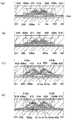
도 1a는 반도체 장치의 구조예를 도시한다. 트랜지스터(250)는 기판(200) 위에 제공된 산화물 반도체층(206a); 상기 산화물 반도체층(206a)에 전기적으로 접속된 소스 또는 드레인 전극(208a) 및 소스 또는 드레인 전극(208b); 상기 산화물 반도체층(206a), 상기 소스 또는 드레인 전극(208a), 및 상기 소스 또는 드레인 전극(208b)을 덮도록 제공된 게이트 절연층(212); 및 상기 산화물 반도체층(206a)과 중첩하도록 상기 게이트 절연층(212) 위에 제공된 게이트 전극(214)을 포함한다. 층간 절연층(216) 및 층간 절연층(218)이 상기 트랜지스터(250)를 덮도록 제공된다. 하지(base)의 역할을 하는 절연층(202)이 상기 기판(200)과 상기 산화물 반도체층(206a) 사이에 제공될 수 있음을 유념한다.1A shows a structural example of a semiconductor device. The
상기 트랜지스터(250)에서, 상기 산화물 반도체층(206a)은 비정질 구조를 가진다. 상기 트랜지스터(250)의 채널 길이(L)는 10nm 이상 1000nm 이하, 바람직하게, 10nm 이상 70nm 이하로 설정된다. 이것은 상기 트랜지스터의 상기 채널 길이가 짧아질 때 고속 동작 및 저전력 소비와 같은 유리한 효과들이 얻어질 수 있기 때문이다. 상기 산화물 반도체층(206a)의 두께(tos)는 1nm 이상 50nm 이하, 바람직하게 1nm 이상 30nm 이하, 더욱 바람직하게 1nm 이상 10nm 이하(예를 들면, 3nm 이상 10nm 이하)로 설정된다. 이것은, 이러한 두께를 가진 상기 산화물 반도체층(206a)이 이용될 때 소형화로 인한 쇼트-채널 효과가 억제될 수 있기 때문이다.In the
상기 게이트 절연층(212)의 두께(tox)는, 상기 게이트 절연층(212)에 이용된 재료의 비유전율이 εr이고 상기 게이트 절연층(212)의 상기 두께가 d일 때,εr/d가 0.08(nm-1) 이상 7.9(nm-1) 이하, 바람직하게 0.26(nm-1) 이상 7.9(nm-1) 이하, 더욱 바람직하게 1.3(nm-1) 이상 7.9(nm-1) 이하인 관계식을 만족하는 두께로 설정될 수 있다. 상기 관계식이 만족될 때, 상기 트랜지스터의 동작은 충분히 보장될 수 있다. 예를 들면, 상기 게이트 절연층(212)이 산화 실리콘(상기 비유전율은 약 3.9인 것으로 가정)을 이용하여 형성되는 경우에, 상기 게이트 절연층(212)의 상기 두께는 0.5nm 이상 50nm 이하, 바람직하게, 0.5nm 이상 15nm 이하, 더욱 바람직하게 0.5nm 이상 3nm 이하로 설정될 수 있다.The thickness tox of the
상기 게이트 절연층(212)에 대한 재료로서, 산화 하프늄 또는 산화 탄탈과 같은 고유전 상수(고-k 재료)를 가진 재료가 이용되는 것이 바람직함을 유념한다. 이러한 재료를 이용하여, 상기 게이트 절연층(212)의 상기 두께가 충분히 보장될 때에도 상기 관계식이 만족될 수 있고, 상기 트랜지스터의 동작을 희생하지 않고 게이트 누설이 억제될 수 있다.Note that as the material for the
도 1b는 도 1a의 상기 반도체 장치의 변형예를 도시한다. 트랜지스터(350)는 기판(300) 위에 제공된 제 1 산화물 반도체층(304a) 및 제 2 산화물 반도체층(306a); 상기 제 1 산화물 반도체층(304a) 및 상기 제 2 산화물 반도체층(306a)에 전기적으로 접속된 소스 또는 드레인 전극(308a) 및 소스 또는 드레인 전극(308b); 상기 제 2 산화물 반도체층(306a), 상기 소스 또는 드레인 전극(308a), 및 상기 소스 또는 드레인 전극(308b)을 덮도록 제공된 게이트 절연층(312); 및 상기 제 2 산화물 반도체층(306a)과 중첩하도록 상기 게이트 절연층(312) 위에 제공된 게이트 전극(314)을 포함한다. 층간 절연층(316) 및 층간 절연층(318)이 상기 트랜지스터(350)를 덮도록 제공된다. 하지의 역할을 하는 절연층(302)이 상기 기판(300)과 상기 제 1 산화물 반도체층(304a) 사이에 제공될 수 있음을 유념한다.FIG. 1B shows a modification of the semiconductor device of FIG. 1A. The
도 1b에 도시된 구조 및 도 1a에 도시된 구조는 상기 산화물 반도체층의 결정도가 서로 상이하다. 도 1a의 상기 산화물 반도체층(206a)의 상기 결정도는 비정질인 반면, 도 1b의 상기 제 1 산화물 반도체층(304a) 및 상기 제 2 산화물 반도체층(306a) 각각은 결정 영역이 제공되는 구조를 가진다. 상기 결정 영역은, 상기 산화물 반도체층의 표면에 실질적으로 평행한 ab 면을 가지고, 일부 경우들에서 상기 표면에 실질적으로 수직인 방향으로 c축 배향되는 결정을 포함한다. 여기서, "실질적으로 평행한 방향(substantially parallel direction)"은 평행 방향에서 ±10° 내의 방향을 의미하고, "실질적으로 수직인 방향(substantially perpendicular direction)"은 수직 방향에서 ±10°내의 방향을 의미한다.The structure shown in FIG. 1B and the structure shown in FIG. 1A differ from each other in crystallinity of the oxide semiconductor layer. While the crystallinity of the
도 1b에 도시된 바와 같이, 상기 트랜지스터의 결정을 가진 상기 산화물 반도체층을 이용하여, 전계-효과 이동도 μ > 100cm2/V·s가 달성될 수 있다. 따라서, 도 1b에 도시된 상기 반도체 장치는 고속 동작이 요구되는 논리 회로에 적합하다.As shown in FIG. 1B, using the oxide semiconductor layer with the crystal of the transistor, a field-effect mobility μ> 100 cm2 / V · s can be achieved. Therefore, the semiconductor device shown in FIG. 1B is suitable for logic circuits requiring high speed operation.
상기 트랜지스터의 상기 채널 길이, 상기 산화물 반도체층의 상기 두께, 및 상기 게이트 절연층의 상기 두께와 같은 조건들은 도 1a와 동일하다.Conditions such as the channel length of the transistor, the thickness of the oxide semiconductor layer, and the thickness of the gate insulating layer are the same as in FIG. 1A.
상기 산화물 반도체층이 2층 구조를 가지는 경우가 도 1b에 도시되었지만, 개시된 발명의 일 실시예는 이 구조에 제한되지 않음을 유념한다. 필요한 두께가 상기 제 1 산화물 반도체층(304a)에 의해서만 보장될 수 있는 경우에, 상기 제 2 산화물 반도체층(306a)은 불필요하다. 즉, 상기 산화물 반도체층은 결정 영역을 가진 산화물 반도체층의 단층 구조를 가질 수 있다.Although the case where the oxide semiconductor layer has a two-layer structure is shown in FIG. 1B, it is noted that one embodiment of the disclosed invention is not limited to this structure. If the required thickness can be ensured only by the first
도 1c는 도 1a의 상기 반도체 장치의 변형예를 도시한다. 트랜지스터(450)는 기판(400) 위에 제공된 산화물 반도체층(406a); 상기 산화물 반도체층(406a)에 전기적으로 접속된 소스 또는 드레인 전극(408a) 및 소스 또는 드레인 전극(408b); 상기 소스 또는 드레인 전극(408a) 및 상기 소스 또는 드레인 전극(408b)의 상부들을 덮도록 제공된 절연층(410a) 및 절연층(410b); 상기 산화물 반도체층(406a), 상기 소스 또는 드레인 전극(408a), 상기 소스 또는 드레인 전극(408b) 등을 덮도록 제공된 게이트 절연층(412); 및 상기 산화물 반도체층(406a)과 중첩하도록 상기 게이트 절연층(412) 위에 제공된 게이트 전극(414)을 포함한다. 층간 절연층(416) 및 층간 절연층(418)이 상기 트랜지스터(450)를 덮도록 제공된다. 하지의 역할을 하는 절연층(402)이 상기 기판(400)과 상기 산화물 반도체층(406a) 사이에 제공될 수 있음을 유념한다.FIG. 1C shows a modification of the semiconductor device of FIG. 1A. The
도 1c에 도시된 구조는 상기 절연층(410a) 및 상기 절연층(410b)의 존재에서 도 1a에 도시된 구조와 상이하다. 상기 절연층(410a) 및 상기 절연층(410b)이 제공될 때, 상기 게이트 전극(414)과 상기 소스 또는 드레인 전극(408a) 사이 및 상기 게이트 전극(414)과 상기 소스 또는 드레인 전극(408b) 사이에 형성되는 커패시턴스가 감소될 수 있다.The structure shown in FIG. 1C is different from the structure shown in FIG. 1A in the presence of the insulating
상기 소스 또는 드레인 전극(408a) 및 상기 소스 또는 드레인 전극(408b)은 각각 산화물 영역(411a) 및 산화물 영역(411b)을 가지며, 그 부분들에서 상기 소스 또는 드레인 전극(408a) 및 상기 소스 또는 드레인 전극(408b)은 상기 게이트 절연층(412)과 접촉한다. 상기 산화물 영역들로, 상기 게이트 절연층의 두께 및 그것으로의 결함 있는 피복성의 감소에 의해 유발될 수 있는 상기 게이트 전극(414)과 상기 소스 또는 드레인 전극(408a) 사이 및 상기 게이트 전극(414)과 상기 소스 또는 드레인 전극(408b) 사이의 단락 회로를 방지하는 것이 가능하다. 또한, 상기 산화물 반도체층(406a)과 상기 소스 또는 드레인 전극(408a) 사이의 계면과 상기 산화물 반도체층(406a)과 상기 소스 또는 드레인 전극(408b) 사이의 계면의 전계를 감소시키는 것이 가능하다.The source or
상기 트랜지스터의 상기 채널 길이, 상기 산화물 반도체층의 상기 두께 및 상기 게이트 절연층의 상기 두께와 같은 조건들은 도 1a와 동일하다.Conditions such as the channel length of the transistor, the thickness of the oxide semiconductor layer and the thickness of the gate insulating layer are the same as in FIG. 1A.
도 1d는 도 1b의 상기 반도체 장치의 변형예를 도시한다. 대안적으로, 도 1d는 도 1c의 상기 반도체 장치의 변형예를 도시한다. 트랜지스터(550)는 기판(500) 위에 제공된 제 1 산화물 반도체층(504a) 및 제 2 산화물 반도체층(506a); 상기 제 1 산화물 반도체층(504a) 및 상기 제 2 산화물 반도체층(506a)에 전기적으로 접속된 소스 또는 드레인 전극(508a), 및 소스 또는 드레인 전극(508b); 상기 소스 또는 드레인 전극(508a) 및 상기 소스 또는 드레인 전극(508b)의 상부들을 덮도록 제공된 절연층(510a) 및 절연층(510b); 상기 제 2 산화물 반도체층(506a), 상기 소스 또는 드레인 전극(508a), 상기 소스 또는 드레인 전극(508b) 등을 덮도록 제공된 게이트 절연층(512); 및 상기 제 2 산화물 반도체층(506a)과 중첩하도록 상기 게이트 절연층(512) 위에 제공된 게이트 전극(514)을 포함한다. 층간 절연층(516) 및 층간 절연층(518)이 상기 트랜지스터(550)를 덮도록 제공된다. 하지의 역할을 하는 절연층(502)이 상기 기판(500)과 상기 제 2 산화물 반도체층(506a) 사이에 제공될 수 있음을 유념한다.FIG. 1D shows a modification of the semiconductor device of FIG. 1B. Alternatively, FIG. 1D illustrates a variation of the semiconductor device of FIG. 1C. The
도 1d에 도시된 구조는 상기 절연층(510a) 및 상기 절연층(510b)의 존재에서 도 1b에 도시된 구조와 상이하다. 상기 절연층(510a) 및 상기 절연층(510b)이 제공될 때, 상기 게이트 전극(514)과 상기 소스 또는 드레인 전극(508a) 사이 및 상기 게이트 전극(514)과 상기 소스 또는 드레인 전극(508b) 사이에 형성되는 커패시턴스가 감소될 수 있다.The structure shown in FIG. 1D is different from the structure shown in FIG. 1B in the presence of the insulating
상기 소스 또는 드레인 전극(508a) 및 상기 소스 또는 드레인 전극(508b)은 각각 상기 소스 또는 드레인 전극(508a) 및 상기 소스 또는 드레인 전극(508b)은 상기 게이트 절연층(512)과 접하는 부분들에서 산화물 영역(511a) 및 산화물 영역(511b)을 가진다. 상기 산화물 영역들로, 상기 게이트 절연층의 두께 및 그것으로의 결함 있는 피복성의 감소에 의해 유발될 수 있는 상기 게이트 전극과 상기 소스 전극 사이 및 상기 게이트 전극과 상기 드레인 전극 사이의 단락 회로를 방지하는 것이 가능하다.The source or
도 1d에 도시된 상기 구조 및 상기 도 1c에 도시된 상기 구조는 상기 산화물 반도체층의 결정도가 서로 상이하다. 도 1d의 상기 제 1 산화물 반도체층(504a) 및 상기 제 2 산화물 반도체층(506a) 각각은 결정 영역이 제공되는 구조를 가진다. 상기 결정 영역은, 상기 산화물 반도체층의 표면에 실질적으로 평행한 ab 면을 가지고, 일부 경우들에서 상기 표면에 실질적으로 수직인 방향으로 c축 배향되는 결정을 포함한다. 여기서, "실질적으로 평행한 방향"은 평행 방향에서 ±10° 내의 방향을 의미하고, "실질적으로 수직인 방향"은 수직 방향에서 ±10° 내의 방향을 의미한다.The crystal structure of the oxide semiconductor layer differs from the structure shown in FIG. 1D and the structure shown in FIG. 1C. Each of the first
도 1d에 도시된 바와 같이, 상기 트랜지스터의 결정 영역을 가진 상기 산화물 반도체층을 이용하여, 전계-효과 이동도 μ > 100cm2/V·s가 달성될 수 있다. 따라서, 도 1d에 도시된 상기 반도체 장치는 고속 동작이 요구되는 논리 회로에 적합하다.As shown in FIG. 1D, using the oxide semiconductor layer having the crystal region of the transistor, a field-effect mobility μ> 100 cm2 / V · s can be achieved. Therefore, the semiconductor device shown in FIG. 1D is suitable for logic circuits requiring high speed operation.
상기 트랜지스터의 상기 채널 길이, 상기 산화물 반도체층의 상기 두께 및 상기 게이트 절연층의 상기 두께와 같은 조건들은 도 1a와 동일하다.Conditions such as the channel length of the transistor, the thickness of the oxide semiconductor layer and the thickness of the gate insulating layer are the same as in FIG. 1A.
상기 산화물 반도체층이 2층 구조를 가지는 경우가 도 1d에 도시되었지만, 개시된 발명의 일 실시예는 이 구조에 제한되지 않음을 유념한다. 필요한 두께는 상기 제 1 산화물 반도체층(504a)에 의해서만 보장될 수 있는 경우에, 상기 제 2 산화물 반도체층(506a)은 불필요하다. 즉, 상기 산화물 반도체층은 결정 영역을 가진 산화물 반도체층의 단층 구조를 가질 수 있다.Although the case in which the oxide semiconductor layer has a two-layer structure is shown in FIG. 1D, it is noted that one embodiment of the disclosed invention is not limited to this structure. If the required thickness can only be ensured by the first
이 실시예에 기술된 상기 구조는 소형화에 적합하다. 이 구조를 이용하여, 산화물 반도체를 포함하는 반도체 장치는 양호한 특성들을 유지할 수 있고 소형화를 달성할 수 있다.The structure described in this embodiment is suitable for miniaturization. Using this structure, the semiconductor device including the oxide semiconductor can maintain good characteristics and achieve miniaturization.
이 실시예에 기술된 구조들, 방법들 등은 다른 실시예들에 기술된 구조들, 방법들 등 중 어느 것과 적합하게 조합될 수 있다.The structures, methods, and the like described in this embodiment may be suitably combined with any of the structures, methods, and the like described in other embodiments.
[실시예 2][Example 2]
이 실시예에서, 산화물 반도체(특히, 비정질 구조)를 포함하는 반도체 장치를 제작하기 위한 방법이 기술될 것이다. 특히, 도 1a의 상기 반도체 장치를 제작하기 위한 방법이 도 2a 내지 도 2e를 참조하여 기술될 것이다. 탑-게이트형 트랜지스터가 예로서 기술되지만, 트랜지스터의 구조는 탑-게이트형 구조에 제한되지 않음을 유념한다.In this embodiment, a method for fabricating a semiconductor device including an oxide semiconductor (particularly an amorphous structure) will be described. In particular, the method for fabricating the semiconductor device of FIG. 1A will be described with reference to FIGS. 2A-2E. Although the top-gate transistor is described as an example, it is noted that the structure of the transistor is not limited to the top-gate type structure.
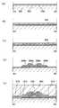
먼저, 상기 절연층(202)이 상기 기판(200) 위에 형성된다. 그 후에, 산화물 반도체층(206)이 상기 절연층(202) 위에 형성된다(도 2a 참조).First, the insulating
상기 기판(200)으로서, 예를 들면, 유리 기판이 이용될 수 있다. 상기 기판(200)으로서, 유리 기판뿐만 아니라, 세라믹 기판, 석영 기판 또는 사파이어 기판과 같은 절연체를 이용하여 형성된 절연 기판, 실리콘과 같은 반도체 재료를 이용하고 그 표면이 절연 재료로 덮이는 반도체 기판, 금속 또는 스테인리스 스틸과 같은 도전체를 이용하여 형성되고 그 표면이 절연 재료로 피복된 도전 기판, 등이 이용될 수 있다. 플라스틱 등을 이용하여 형성된 기판은 일반적으로 낮은 상한 온도를 가지려는 경향이 있지만, 상기 기판이 나중에 수행되는 제작 공정에서의 공정 온도를 견딜 수 있는 한, 상기 기판(200)으로서 이용될 수 있다.As the
상기 기판(200)은 1nm 이하의 산술 평균 편차(Ra)를 가지는 것이 바람직함을 유념한다. 더욱 바람직하게, 상기 기판(200)은 0.5nm 이하의 산술 평균 편차를 가진다. 이러한 이유는 다음과 같다: 패터닝을 위해 이용되는 마스크의 노광 조건에 대한 수요들이 반도체 장치의 소형화에 따라 증가되고, 노광 조건에 대한 상기 수요들이 높은 경우에도, 이들은 높은 평탄성을 가진 이러한 기판을 이용하여 쉽게 충족될 수 있다. 상기 산술 평균 편차에 대해, 예를 들면, 10㎛ × 10㎛의 영역에 대해 수행된 측정에 의해 획득된 값이 이용될 수 있음을 유념한다.Note that the
상기 절연층(202)은 하지로서 기능하고 PVD법, CVD법 등에 의해 형성될 수 있다. 상기 절연층(202)은 산화 실리콘, 산화질화 실리콘, 질화 실리콘, 산화 하프늄, 산화 알루미늄 또는 산화 탄탈과 같은 무기 절연 재료를 함유한 재료를 이용하여 형성될 수 있다. 상기 절연층(202)이 수소 또는 수분을 가능한 적게 함유하도록 형성하는 것이 바람직함을 유념한다. 상기 절연층(202)이 제공되지 않는 구조도 또한 가능하다.The insulating
상기 산화물 반도체층(206)으로서, 4원계 금속 산화물인 In-Sn-Ga-Zn-O계 산화물 반도체; 3원계 금속 산화물들인 In-Ga-Zn-O계 산화물 반도체, In-Sn-Zn-O계 산화물 반도체, In-Al-Zn-O계 산화물 반도체, Sn-Ga-Zn-O계 산화물 반도체, Al-Ga-Zn-O계 산화물 반도체 또는 Sn-Al-Zn-O계 산화물 반도체; 2원계 금속 산화물들인 In-Zn-O계 산화물 반도체, Sn-Zn-O계 산화물 반도체, Al-Zn-O계 산화물 반도체, Zn-Mg-O계 산화물 반도체, Sn-Mg-O계 산화물 반도체 또는 In-Mg-O계 산화물 반도체; 또는 In-O계 산화물 반도체, Sn-O계 산화물 반도체 또는 Zn-O계 산화물 반도체가 이용될 수 있다.As the
특히, In-Ga-Zn-O계 산화물 반도체 재료는 전계가 존재하지 않고 따라서 오프 전류가 충분히 감소될 수 있을 때 충분히 높은 저항을 가진다. 또한, 높은 전계 이동도를 가져서, 상기 In-Ga-Zn-O계 산화물 반도체 재료는 반도체 장치에 이용되는 반도체 재료에 적합하다.In particular, the In—Ga—Zn—O based oxide semiconductor material has a sufficiently high resistance when no electric field is present and thus the off current can be sufficiently reduced. In addition, having high field mobility, the In—Ga—Zn—O-based oxide semiconductor material is suitable for semiconductor materials used in semiconductor devices.
상기 In-Ga-Zn-O계 산화물 반도체 재료의 전형적인 예로서, InGaO3(ZnO)m(m > 0)에 의해 표현되는 산화물 반도체 재료가 존재한다. 또한, M이 Ga 대신 이용될 때, InMO3(ZnO)m(m > 0)에 의해 표현되는 산화물 반도체 재료가 존재한다. 여기서, M은 갈륨(Ga), 알루미늄(Al), 철(Fe), 니켈(Ni), 망간(Mn), 코발트(Co) 등으로부터 선택된 하나 이상의 금속 원소들을 표시한다. 예를 들면, M은 Ga, Ga 및 Al, Ga 및 Fe, Ga 및 Ni, Ga 및 Mn, Ga 및 Co 등일 수 있다. 상술된 조성비들은 상기 산화물 반도체 재료가 가질 수 있는 결정 구조들로부터 도출되고 단지 예들일 뿐이라는 것을 유념한다.As a typical example of the In-Ga-Zn-O-based oxide semiconductor material, there is an oxide semiconductor material represented by InGaO3 (ZnO)m (m> 0). In addition, when M is used instead of Ga, there is an oxide semiconductor material represented by InMO3 (ZnO)m (m> 0). Here, M represents one or more metal elements selected from gallium (Ga), aluminum (Al), iron (Fe), nickel (Ni), manganese (Mn), cobalt (Co) and the like. For example, M can be Ga, Ga and Al, Ga and Fe, Ga and Ni, Ga and Mn, Ga and Co and the like. Note that the above composition ratios are derived from the crystal structures that the oxide semiconductor material may have and are merely examples.
스퍼터링 방법에 의해 상기 산화물 반도체층(206)을 형성하기 위한 타겟으로서, In : Ga : Zn = 1 : x : y (x는 0 이상이고, y는 0.5 이상 5 이하임)의 조성비를 가진 타겟이 바람직하다. 예를 들면, In : Ga : Zn = 1 : 1 : 1[원자수비] (x = 1, y = 1)(즉, In2O3 : Ga2O3 : ZnO = 1 : 1 : 2[몰수비])의 조성비를 가진 타겟이 이용될 수 있다. 대안적으로, In : Ga : Zn = 1 : 1 : 0.5[원자수비] (x = 1, y = 0.5)(즉, In2O3 : Ga2O3 : ZnO = 1 : 1 : 1[몰수비])의 조성비를 가진 타겟; In : Ga : Zn = 1 : 1 : 2(x = 1, y = 2)[원자수비](즉, In2O3 : Ga2O3 : ZnO = 1 : 1 : 4[몰수비])의 조성비를 가진 타겟; 또는 In : Ga : Zn = 1 : 0 : 1[원자수비] (x = 0, y = 1)(즉, In2O3 : ZnO = 1 : 2[몰수비])의 조성비를 가진 타겟이 이용될 수 있다.As a target for forming the
이 실시예에서, 비정질 구조를 가진 상기 산화물 반도체층(206)은 In-Ga-Zn-O계 금속 산화물 타겟을 이용하여 스퍼터링 방법에 의해 형성된다.In this embodiment, the
상기 금속 산화물 타겟의 금속 산화물의 상대 밀도는 80% 이상, 바람직하게 95% 이상, 더욱 바람직하게 99.9% 이상이다. 높은 상대 밀도를 가진 금속 산화물 타겟의 이용은 조밀한 구조를 가진 상기 금속 산화물 반도체층(206)을 형성하는 것을 가능하게 한다.The relative density of the metal oxide of the metal oxide target is at least 80%, preferably at least 95%, more preferably at least 99.9%. Use of a metal oxide target with a high relative density makes it possible to form the metal
상기 산화물 반도체층(206)이 형성되는 분위기는 희가스 분위기(통상적으로, 아르곤) 분위기, 산소 분위기, 또는 희가스(통상적으로, 아르곤)와 산소의 혼합 분위기가 바람직하다. 특히, 그 농도가 1ppm 이하(바람직하게 10ppb 이하)로 감소되도록, 수소, 수분, 수산기, 및 수소화물과 같은 불순물들이 제거된 고순도 가스 분위기를 이용하는 것이 바람직하다.The atmosphere in which the
상기 산화물 반도체층(206)을 형성할 때, 예를 들면, 상기 기판은 감압 상태에서 유지되는 처리 챔버에서 유지되고, 상기 기판은 100℃ 이상 550℃ 이하, 바람직하게, 200℃ 이상 400℃ 이하의 온도로 가열된다. 대안적으로, 상기 산화물 반도체층(206)을 형성할 때의 기판 온도는 실내 온도일 수 있다. 그 후에, 상기 처리 챔버의 습기가 제거되는 동안, 수소, 수분 등이 제거된 스퍼터링 가스가 상기 처리 챔버에 도입되고, 그에 의해, 상기 산화물 반도체층(206)은 상술된 타겟을 이용하여 형성된다. 상기 산화물 반도체층(206)은 상기 기판이 가열되는 동안에 형성되어, 상기 산화물 반도체층(206)에 함유된 불순물들이 감소될 수 있다. 또한, 상기 스퍼터링으로 인한 손상이 감소될 수 있다. 상기 처리 챔버에서 습기를 제거하기 위해, 흡착형 진공 펌프가 이용되는 것이 바람직하다. 예를 들면, 크라이오펌프, 이온 펌프, 티타늄 서블리메이션 펌프 등이 이용될 수 있다. 대안적으로, 냉각 트랩이 구비된 터보 펌프가 이용될 수 있다. 크라이오펌프 등을 이용하여, 수소, 수분 등이 상기 처리 챔버에서 제거될 수 있다; 따라서, 상기 산화물 반도체층(206)에서의 상기 불순물 농도가 감소될 수 있다.When the
예를 들면, 상기 산화물 반도체층(206)을 형성하기 위한 조건들은 다음과 같이 설정될 수 있다: 상기 기판과 상기 타겟 사이의 간격은 170mm이고, 압력은 0.4Pa이고, 직류(DC) 전력은 0.5kW이고, 온도는 산소(100% 산소) 분위기, 아르곤(100% 아르곤) 분위기, 또는 산소와 아르곤의 혼합 분위기이다. 먼지(상기 막 형성시에 형성되는 가루 물질들)가 감소될 수 있고 상기 막 두께가 균일해질 수 있기 때문에 펄스식 직류(DC) 전원이 이용되는 것이 바람직함을 유념한다. 상기 산화물 반도체층(206)의 상기 두께는 1nm 이상 50nm 이하, 바람직하게 1nm 이상 30nm 이하, 더욱 바람직하게 1nm 이상 10nm 이하(예를 들면, 3nm 이상 10nm 이하)이다. 이러한 두께를 가진 상기 산화물 반도체층(206)을 사용하여, 최소화로 인한 쇼트-채널 효과가 억제될 수 있다. 상기 산화물 반도체에 대한 상기 재료, 상기 반도체 장치의 사용 등에 의존하여 적합한 두께가 변경될 수 있고, 따라서, 상기 두께는 상기 재료, 상기 사용 등에 의존하여 적합하게 선택될 수 있음을 유념한다.For example, the conditions for forming the
상기 산화물 반도체층(206)이 스퍼터링 방법에 의해 형성되기 전에, 플라즈마가 도입된 아르곤 가스로 생성되는 역 스퍼터링이 바람직하게 수행되어, 상기 산화물 반도체층(206)이 형성되는 표면(예를 들면, 상기 절연층(202)의 표면)에 부착된 먼지가 제거된다. 여기서, 상기 역 스퍼터링은 상기 표면이 변형되도록 이온들이 가공될 표면과 충돌하는 방법이며, 이것은 이온들이 스퍼터링 타겟과 충돌하는 보통의 스퍼터링과 대조된다. 이온들이 가공될 표면과 충돌하게 하기 위한 방법의 예는, 플라즈마가 기판 근처에서 생성되도록 고주파수 전압이 아르곤 분위기에서 상기 표면에 인가되는 방법이다. 질소, 헬륨, 산소 등의 분위기는 아르곤 분위기 대신에 이용될 수 있음을 유념한다.Before the
다음에, 상기 산화물 반도체층(206)은 마스크를 이용한 에칭과 같은 방법에 의해 가공된다; 따라서, 섬형 산화물 반도체층(206a)이 형성된다.Next, the
상기 산화물 반도체층(206)을 에칭하기 위한 방법으로서, 건식 에칭 또는 습식 에칭이 이용될 수 있다. 건식 에칭 및 습식 에칭은 조합하여 이용될 수 있음은 말할 필요도 없다. 에칭 조건들(예를 들면, 에칭 가스 또는 에천트, 에칭 시간, 및 온도)은 상기 산화물 반도체층이 원하는 형상으로 에칭될 수 있도록 상기 재료에 의존하여 적합하게 설정된다.As a method for etching the
건식 에칭에 이용되는 에칭 가스의 예는 염소를 함유한 가스(염소(Cl2), 3염화 붕소(BCl3), 4염화 실리콘(SiCl4), 또는 4염화 탄소(CCl4)와 같은 염소계 가스)이다. 또한, 플루오르를 함유한 가스(4플루오르화 탄소(CF4), 6플루오르화 황(SF6), 3플루오르화 질소(NF3), 또는 3플루오로메탄(CHF3)과 같은 플루오르계 가스), 브롬화 수소(HBr), 산소(O2), 헬륨(He) 또는 아르곤(Ar)과 같은 희가스가 첨가되는 이들 가스들 중 어느 하나 등이 이용될 수 있다.Examples of etching gases used for dry etching are chlorine-based gases such as chlorine containing gas (chlorine (Cl2 ), boron trichloride (BCl3 ), silicon tetrachloride (SiCl4 ), or carbon tetrachloride (CCl4 )). )to be. Also, fluorine-containing gas (fluorine-based gas such as carbon tetrafluoride (CF4 ), sulfur hexafluoride (SF6 ), nitrogen trifluoride (NF3 ), or trifluoromethane (CHF3 )). Any one of these gases to which a rare gas such as hydrogen bromide (HBr), oxygen (O2 ), helium (He), or argon (Ar) is added may be used.
상기 건식 에칭 방법으로서, 평행평판형 RIE(reactive ion etching) 방법 또는 ICP(inductively coupled plasma) 에칭 방법이 이용될 수 있다. 상기 산화물 반도체층을 원하는 형상으로 에칭하기 위해, 에칭 조건들(예를 들면, 코일형 전극에 인가된 전력량, 기판측 상의 전극에 인가된 전력량, 및 상기 기판측 상의 전극 온도)이 적합하게 설정된다.As the dry etching method, a parallel plate type reactive ion etching (RIE) method or an inductively coupled plasma (ICP) etching method may be used. In order to etch the oxide semiconductor layer into a desired shape, etching conditions (e.g., the amount of power applied to the coiled electrode, the amount of power applied to the electrode on the substrate side, and the electrode temperature on the substrate side) are suitably set. .
상기 습식 에칭에 이용된 에천트로서, 인산, 아세트산 및 질산을 혼합하여 얻어진 용액, 암모니아 과산화 혼합(31wt%의 과산화수소수 : 28wt%의 암모니아수 : 물 = 5 : 2 : 2) 등이 이용될 수 있다. ITO-07N(KANTO CHEMICAL CO., INC.에 의해 생산됨)과 같은 에천트도 또한 이용될 수 있다.As the etchant used for the wet etching, a solution obtained by mixing phosphoric acid, acetic acid and nitric acid, ammonia peroxide mixture (31 wt% hydrogen peroxide: 28 wt% aqueous ammonia: water = 5: 2: 2) and the like can be used. . An etchant such as ITO-07N (produced by KANTO CHEMICAL CO., INC.) May also be used.
에칭은 상기 산화물 반도체층(206a)의 단부가 테이퍼 형상을 가지도록 수행되는 것이 바람직하다. 여기서, 테이퍼 각은 예를 들면 30° 이상 60°가 바람직하다. 상기 "테이퍼 각(tapered angle)"은 단면에 수직인 방향(기판의 표면에 수직인 평면)으로 관찰될 때 테이퍼 형상을 가진 층(예를 들면, 상기 산화물 반도체층(206a))의 측면 및 저면에 의해 형성된 입사각을 의미한다. 상기 산화물 반도체층(206a)의 상기 단부가 테이퍼 형상을 가지도록 상기 에칭이 수행되고, 그에 의해 나중에 형성되는 상기 소스 또는 드레인 전극(208a) 및 상기 소스 또는 드레인 전극(208b)이 개선되고, 접속해제가 방지될 수 있다.Etching is preferably performed such that an end portion of the
그 후, 열 처리(제 1 열 처리)가 상기 산화물 반도체층(206a)에 대해 수행되는 것이 바람직하다. 상기 제 1 열 처리를 통해, 상기 산화물 반도체층(206a)에서의 과잉 산소(물 또는 수산기를 포함)가 제거되고, 상기 산화물 반도체층(206a)의 구조가 개선되고, 에너지 갭의 결함 준위가 감소될 수 있다. 상기 제 1 열 처리의 온도는 300℃ 이상 550℃ 이하, 또는 400℃ 이상 500℃ 이하로 설정된다. 여기에 기술된 바와 같이, 상기 에칭 후에 상기 열 처리(제 1 열 처리)가 수행되는 경우에, 상기 에칭은 습식 에칭이 이용될 때에도 높은 에칭율로 수행될 수 있고, 따라서 상기 에칭에 요구되는 시간이 단축될 수 있는 이점이 있음을 유념한다.Then, heat treatment (first heat treatment) is preferably performed on the
예를 들면, 상기 기판(200)이 저항 발열체 등을 포함하는 전기로에 도입된 후에, 상기 열 처리는 450℃로 1 시간 동안 질소 분위기에서 수행될 수 있다. 상기 산화물 반도체층(206a)은 수분 또는 수소의 혼입이 방지될 수 있도록 상기 열 처리 동안 대기에 노출되지 않는다.For example, after the
상기 열 처리 장치는 반드시 상기 전기로에 제한될 필요가 없고 가열된 가스와 같은 매체로부터 열 복사 또는 열 전도에 의해 가공될 대상을 가열하기 위한 장치일 수 있다. 예를 들면, 램프 급속 열 어닐(LRTA) 장치 또는 가스 급속 열 어닐(GRTA) 장치와 같은 급속 열 어닐(RTA) 장치가 이용될 수 있다. LRTA 장치는 할로겐 램프, 금속 할라이드 램프, 크세논 아크 램프, 탄소 아크 램프, 고압 나트륨 램프, 또는 고압 수은 램프와 같은 램프로부터 방출된 광의 복사(전자파)에 의해 가공될 대상을 가열하기 위한 장치이다. GRTA 장치는 고온 가스를 이용하여 열 처리를 수행하기 위한 장치이다. 상기 가스로서, 질소 또는 아르곤과 같은 희가스와 같이, 열 처리에 의해 가공될 대상과 반응하지 않는 불활성 가스가 이용된다.The heat treatment device need not necessarily be limited to the electric furnace and can be a device for heating the object to be processed by heat radiation or heat conduction from a medium such as a heated gas. For example, rapid thermal anneal (RTA) devices such as lamp rapid thermal anneal (LRTA) devices or gas rapid thermal anneal (GRTA) devices can be used. LRTA devices are devices for heating objects to be processed by radiation (electromagnetic waves) of light emitted from lamps such as halogen lamps, metal halide lamps, xenon arc lamps, carbon arc lamps, high pressure sodium lamps, or high pressure mercury lamps. The GRTA apparatus is a apparatus for performing heat treatment using hot gas. As the gas, an inert gas that does not react with the object to be processed by heat treatment, such as a rare gas such as nitrogen or argon, is used.
예를 들면, 상기 제 1 열 처리로서, GRTA가 다음과 같이 수행될 수 있다. 상기 기판이 가열된 불활성 가스 분위기에 배치되고, 수 분 동안 가열되고, 상기 가열된 불활성 가스 분위기로부터 꺼내어진다. GRTA는 단기간 동안의 고온 가열 처리를 가능하게 한다. 또한, 이러한 열 처리는 단시간만 취하기 때문에 온도가 상기 기판의 온도 상한을 초과할 때에도 적용 가능하다. 상기 불활성 가스는 상기 공정 동안 산소를 함유한 가스로 변경될 수 있음을 유념한다. 이것은 산소 결핍으로 인한 에너지 갭의 결함 정도가 산소를 함유한 분위기에서 상기 제 1 열 처리에 의해 감소될 수 있기 때문이다.For example, as the first heat treatment, GRTA can be performed as follows. The substrate is placed in a heated inert gas atmosphere, heated for several minutes, and taken out of the heated inert gas atmosphere. GRTA allows for high temperature heat treatment for a short time. In addition, since such heat treatment takes only a short time, it is also applicable when the temperature exceeds the upper temperature limit of the substrate. Note that the inert gas can be changed to a gas containing oxygen during the process. This is because the degree of defects in the energy gap due to oxygen deficiency can be reduced by the first heat treatment in an atmosphere containing oxygen.
상기 불활성 가스 분위기로서, 질소 또는 희가스(예를 들면, 헬륨, 네온 또는 아르곤)를 주성분으로 함유하고 수분, 수소 등을 함유하지 않는 분위기가 이용되는 것이 바람직함을 유념한다. 예를 들면, 상기 가열 처리 장치에 도입된 질소, 또는 헬륨, 네온 또는 아르곤과 같은 희가스의 순도는 6N(99.9999%) 이상이고, 바람직하게는 7N(99.99999%) 이상이다(즉, 불순물들의 농도는 1ppm 이하, 바람직하게는 0.1ppm 이하이다).Note that, as the inert gas atmosphere, an atmosphere containing nitrogen or a rare gas (for example, helium, neon or argon) as a main component and containing no moisture, hydrogen, or the like is preferably used. For example, the purity of nitrogen introduced into the heat treatment device, or a rare gas such as helium, neon or argon, is at least 6N (99.9999%), preferably at least 7N (99.99999%) (ie, the concentration of impurities is 1 ppm or less, preferably 0.1 ppm or less).
어떤 경우든, 상기 불순물들은 상기 제 1 열 처리에 의해 감소되어, i-형 반도체층(진성 반도체층) 또는 실질적으로 i-형 반도체층인 상기 산화물 반도체층(206a)이 형성된다. 따라서, 극히 우수한 특성들을 가진 트랜지스터들이 실현될 수 있다.In any case, the impurities are reduced by the first heat treatment to form the
상기 제 1 열 처리는 아직 상기 섬형 산화물 반도체층(206a)으로 가공되지 않은 상기 산화물 반도체층(206)에 대해 수행될 수 있음을 유념한다. 그 경우, 상기 제 1 열 처리 후에, 상기 기판(200)은 상기 가열 장치로부터 꺼내어지고 포토리소그래피 단계가 수행된다.Note that the first heat treatment may be performed on the
상기 열 처리(상기 제 1 열 처리)는, 수소 또는 수분을 제거하는 효과가 있기 때문에 또한 탈수화 처리, 탈수소화 처리 등이라고 칭해질 수 있다. 상기 탈수화 처리 또는 탈수소화 처리는 또한 상기 산화물 반도체층(206a)이 형성된 후, 또는 상기 소스 전극 및 상기 드레인 전극이 상기 산화물 반도체층(206a) 위에 적층된 후에 수행될 수 있다. 이러한 탈수화 처리 또는 탈수소화 처리는 1회보다 많이 수행될 수 있다.The heat treatment (the first heat treatment) may also be referred to as dehydration treatment, dehydrogenation treatment, or the like because of its effect of removing hydrogen or water. The dehydration treatment or dehydrogenation treatment may also be performed after the
다음에, 도전층이 상기 산화물 반도체층(206a)과 접촉하여 형성된다. 그 후에, 상기 도전층은 상기 소스 또는 드레인 전극(208a) 및 상기 소스 또는 드레인 전극(208b)을 형성하도록 선택적으로 에칭된다(도 2b 참조).Next, a conductive layer is formed in contact with the
상기 도전층은 스퍼터링법과 같은 PVD법 또는 플라즈마 CVD법과 같은 CVD법에 의해 형성될 수 있다. 상기 도전층의 재료로서, 알루미늄, 크롬, 구리, 탄탈, 티타늄, 몰리브덴 및 텅스텐으로부터 선택된 원소, 상기 원소들 중 어느 것을 구성성분으로 함유한 합금 등이 이용될 수 있다. 대안적으로, 망간, 마그네슘, 지르코늄 및 베릴륨으로부터 선택된 하나 이상의 재료들이 이용될 수 있다. 또한, 대안적으로, 티타늄, 탄탈, 텅스텐, 몰리브덴, 크롬, 네오디뮴, 및 스칸듐으로부터 선택된 하나 이상의 원소들과 조합된 알루미늄이 이용될 수 있다.The conductive layer may be formed by a PVD method such as sputtering or a CVD method such as plasma CVD. As the material of the conductive layer, an element selected from aluminum, chromium, copper, tantalum, titanium, molybdenum and tungsten, an alloy containing any one of the above elements as a constituent, and the like can be used. Alternatively, one or more materials selected from manganese, magnesium, zirconium and beryllium may be used. Alternatively, aluminum in combination with one or more elements selected from titanium, tantalum, tungsten, molybdenum, chromium, neodymium, and scandium may be used.
상기 도전층은 단층 구조 또는 둘 이상 층들의 적층 구조를 가질 수 있다. 예를 들면, 티타늄막 또는 질화 티타늄막의 단층 구조, 실리콘을 함유한 알루미늄막의 단층 구조, 티타늄막이 알루미늄막 위에 적층된 2층 구조, 티타늄막이 티타늄 질화막 위에 적층된 2층 구조, 티타늄막, 알루미늄막 및 티타늄막이 이 순서로 적층된 3층 구조 등이 주어질 수 있다. 상기 도전층은 티타늄막 또는 질화 티타늄막의 단층 구조를 가지는 경우에, 상기 도전층은 각각이 테이퍼 형상을 가진 상기 소스 또는 드레인 전극(208a) 및 상기 소스 또는 드레인 전극(208b)으로 용이하게 가공될 수 있다는 이점이 있음을 유념한다.The conductive layer may have a single layer structure or a stacked structure of two or more layers. For example, a single layer structure of a titanium film or a titanium nitride film, a single layer structure of an aluminum film containing silicon, a two-layer structure in which a titanium film is laminated on an aluminum film, a two-layer structure in which a titanium film is stacked on a titanium nitride film, a titanium film, an aluminum film and A three layer structure in which a titanium film is laminated in this order can be given. When the conductive layer has a single layer structure of a titanium film or a titanium nitride film, the conductive layer can be easily processed into the source or
상기 도전층은 또한, 도전성 금속 산화물을 이용하여 형성될 수 있다. 상기 도전성 금속 산화물로서, 산화 인듐(In2O3), 산화 주석(SnO2), 산화 아연(ZnO), 산화 인듐-산화 주석 합금(In2O3-SnO2, 이것은 일부 경우들에서 ITO로 축약됨), 산화 인듐-산화 아연 합금(In2O3-ZnO), 또는 실리콘 또는 산화 실리콘이 함유된 이들 금속 산화물 재료들 중 어느 것이 이용될 수 있다.The conductive layer may also be formed using a conductive metal oxide. As the conductive metal oxide, indium oxide (In2 O3 ), tin oxide (SnO2 ), zinc oxide (ZnO), indium oxide-tin oxide alloy (In2 O3 -SnO2 , which in some cases is referred to as ITO Abbreviated), indium oxide-zinc oxide alloy (In2 O3 -ZnO), or any of these metal oxide materials containing silicon or silicon oxide can be used.
상기 도전층은 형성될 상기 소스 또는 드레인 전극(208a) 및 상기 소스 또는 드레인 전극(208b)의 단부들이 테이퍼 형상을 가지도록 에칭되는 것이 바람직하다. 여기서, 테이퍼 각은 예를 들면 30°이상 60°이하가 바람직하다. 상기 소스 또는 드레인 전극(208a) 및 상기 소스 또는 드레인 전극(208b)의 상기 단부들이 테이퍼 형상을 가지도록 상기 에칭이 수행되고, 그에 의해 나중에 형성되는 상기 게이트 절연층(212)으로의 피복성이 개선되고, 접속해제가 방지될 수 있다.The conductive layer is preferably etched such that end portions of the source or
상기 트랜지스터의 상기 채널 길이(L)는 상기 소스 또는 드레인 전극(208a)의 하부 에지부와 상기 소스 또는 드레인 전극(208b)의 하부 에지부 사이의 간격에 의해 결정된다. 상기 채널 길이(L)가 25nm 미만인 경우의 노광에 대해, 마스크를 형성하기 위한 노광이 파장이 짧은 수 나노미터들 내지 수십 나노미터들인 초자외선으로 수행되는 것이 바람직함을 유념한다. 초자외선으로의 노광은 고해상도 및 큰 초점 깊이를 유발한다. 따라서, 나중에 형성될 상기 트랜지스터의 상기 채널 길이(L)는 10nm 이상 1000nm(1㎛) 이하, 예를 들면 10nm 이상 70nm 이하일 수 있고, 따라서, 회로의 동작 속도가 증가될 수 있다. 또한, 상기 반도체 장치의 전력 소비가 소형화로 인해 감소될 수 있다.The channel length L of the transistor is determined by the distance between the lower edge portion of the source or
상기 소스 또는 드레인 전극(208a) 및 상기 소스 또는 드레인 전극(208b) 위에 절연층이 형성될 수 있음을 유념한다. 상기 절연층이 제공될 때, 나중에 형성될 상기 게이트 전극과 상기 소스 또는 드레인 전극(208a) 사이 및 상기 게이트 전극과 상기 소스 또는 드레인 전극(208b) 사이의 기생 용량이 감소될 수 있다.Note that an insulating layer may be formed on the source or
다음에, 상기 게이트 절연층(212)은 상기 산화물 반도체층(206a)의 일부와 접촉하여 형성된다(도 2c 참조). 상기 게이트 절연층(212)은 CVD법, 스퍼터링법 등에 의해 형성될 수 있다. 상기 게이트 절연층(212)은 산화 실리콘, 질화 실리콘, 산화질화 실리콘, 산화 알루미늄, 산화 탄탈, 산화 하프늄, 산화 이트륨, 하프늄 실리케이트(HfSixOy(x > 0, y > 0)), 질소가 첨가된 하프늄 실리케이트(HfSixOy(x > 0, y > 0)), 질소가 첨가된 하프늄 알루미네이트(HfAlxOy(x > 0, y > 0)) 등을 함유하도록 형성되는 것이 바람직하다. 상기 게이트 절연층(212)은 단층 구조 또는 적층 구조를 가질 수 있다. 상기 반도체 장치가 소형화되는 경우, 상기 게이트 절연층(212)은 상기 트랜지스터의 동작을 보장하기 위해 얇은 것이 바람직하다. 예를 들면, 산화 실리콘이 이용되는 경우에, 그 두께는 0.5nm 이상 50nm 이하, 바람직하게 0.5nm 이상 15nm 이하, 더욱 바람직하게 0.5nm 이상 3nm 이하일 수 있다.Next, the
상기 게이트 절연막이 상술된 바와 같이 얇게 형성될 때, 터널 효과 등으로 인한 게이트 누설이 문제가 된다. 게이트 누설의 문제를 해결하기 위해, 상기 게이트 절연층(212)은 산화 하프늄, 산화 탄탈, 산화 이트륨, 하프늄 실리케이트(HfSixOy(x > 0, y > 0)), 질소가 첨가된 하프늄 실리케이트(HfSixOy(x > 0, y > 0))또는 질소가 첨가된 하프늄 알루미네이트(HfAlxOy(x > 0, y > 0))과 같은 고 유전 상수(고-k 재료)를 가진 재료를 이용하여 형성되는 것이 바람직하다. 상기 게이트 절연층(212)에 대해 고 유전 상수(고-k 재료)를 가진 재료를 이용하여, 상기 게이트 절연층(212)의 두께는 전기 특성들을 보장하고 게이트 누설을 방지하도록 클 수 있다. 상기 게이트 절연층(212)은 고 유전 상수(고-k 재료)를 가진 재료를 함유한 막과, 산화 실리콘, 질화 실리콘, 산화질화 실리콘, 질화산화 실리콘, 산화 알루미늄 등을 함유하는 막의 적층 구조를 가질 수 있음을 유념한다.When the gate insulating film is formed thin as described above, the gate leakage due to the tunnel effect or the like becomes a problem. In order to solve the gate leakage problem, the
상기 게이트 절연층(212)의 두께는, 상기 게이트 절연층(212)에 이용된 재료의 비유전율이 εr이고 상기 게이트 절연층(212)의 두께가 d일 때,εr/d가 0.08(nm-1) 이상 7.9(nm-1) 이하, 바람직하게 0.26(nm-1) 이상 7.9(nm-1) 이하, 더욱 바람직하게 1.3(nm-1) 이상 7.9(nm-1) 이하인 관계식을 만족하는 두께로 설정될 수 있다. 상기 조건은 산화 실리콘(상기 비유전율은 약 3.9인 것으로 가정)이 이용되는 경우에, 상기 게이트 절연층(212)의 상기 두께는 0.5nm 이상 50nm 이하, 바람직하게, 0.5nm 이상 15nm 이하, 더욱 바람직하게 0.5nm 이상 3nm 이하인 조건에 실질적으로 대응함을 유념한다.The thickness of the
상기 게이트 절연층(212)이 형성된 후에, 제 2 열 처리가 불활성 가스 분위기 또는 산소 분위기에서 수행되는 것이 바람직하다. 상기 제 2 열 처리의 온도는 200℃ 이상 450℃ 이하, 바람직하게 250℃ 이상 350℃ 이하이다. 예를 들면, 상기 제 2 열 처리는 250℃로 1시간 동안 질소 분위기에서 수행될 수 있다. 상기 제 2 열 처리는 상기 트랜지스터의 전기 특성들의 변동을 감소시킬 수 있다. 상기 게이트 절연층(212)이 산소를 함유하는 경우에, i-형 산화물 반도체층(진성 반도체층) 또는 실질적으로 i-형 반도체층인 상기 산화물 반도체층(206a)이 형성될 수 있도록, 상기 산화물 반도체층(206a)에 산소를 공급하고 상기 산화물 반도체층(206a)에서 산소 결손을 보상하는 것이 가능하다.After the
상기 제 2 열 처리는 이 실시예에서 상기 게이트 절연층(212)이 형성된 후에 수행되지만, 상기 제 2 열 처리의 타이밍은 이에 특별히 제한되지 않는다. 예를 들면, 상기 제 2 열 처리는 상기 게이트 전극(214)이 형성된 후에 수행될 수 있다.The second heat treatment is performed after the
다음에, 상기 게이트 전극(214)이 상기 산화물 반도체층(206a)과 중첩하는 영역에서 상기 게이트 절연층(212) 위에 형성된다(도 2d 참조). 상기 게이트 전극(214)은 도전층이 상기 게이트 절연층(212) 위에 형성된 다음 선택적으로 패터닝되는 방식으로 형성될 수 있다. 상기 게이트 전극(214)이 될 상기 도전층은 스퍼터링법과 같은 PVD법 또는 플라즈마 CVD법과 같은 CVD법에 의해 형성될 수 있다. 상세들은 상기 소스 또는 드레인 전극(208a), 상기 소스 또는 드레인 전극(208b) 등을 형성하기 위한 상세들과 유사하고, 그 기술이 참조될 수 있다.Next, the
다음에, 상기 층간 절연층(216) 및 상기 층간 절연층(218)이 상기 게이트 절연층(212) 및 상기 게이트 전극(214) 위에 형성된다(도 2e 참조). 상기 층간 절연층들(216 및 218)은 PVD법, CVD법 등에 의해 형성될 수 있다. 상기 층간 절연층들(216 및 218)은 산화 실리콘, 산화질화 실리콘, 질화 실리콘, 산화 하프늄, 산화 알루미늄 또는 산화 탄탈과 같은 무기 절연 재료를 함유한 재료를 이용하여 형성될 수 있다. 이 실시예에서, 상기 층간 절연층들(216 및 218)이 적층되지만, 개시된 발명의 일 실시예는 이 예에 제한되지 않음을 유념한다. 단층 구조 또는 3개 이상의 층들의 적층 구조도 또한 이용될 수 있다. 대안적으로, 상기 층간 절연층은 생략될 수 있다.Next, the
상기 층간 절연층(218)은 평탄화된 표면을 가지도록 형성되는 것이 바람직함을 유념한다. 이것은, 예를 들면 상기 반도체 장치가 소형화되는 경우에도 상기 층간 절연층(218) 위에 전극, 배선 등이 양호하게 형성될 수 있기 때문이다. 상기 층간 절연층(218)은 화학 기계적 연마(CMP)와 같은 방법을 이용하여 평탄화될 수 있다.Note that the interlayer insulating
상기 단계들을 통해, 고순도화된 산화물 반도체층(206a)을 포함하는 상기 트랜지스터(250)가 완성된다(도 2e 참조).Through the above steps, the
도 2e에 도시된 상기 트랜지스터(250)는 상기 절연층(202)을 사이에 구비하여 상기 기판(200) 위에 제공된 상기 산화물 반도체층(206a); 상기 산화물 반도체층(206a)에 전기적으로 접속된 상기 소스 또는 드레인 전극(208a) 및 상기 소스 또는 드레인 전극(208b); 상기 산화물 반도체층(206a), 상기 소스 또는 드레인 전극(208a), 및 상기 소스 또는 드레인 전극(208b)을 덮도록 제공된 상기 게이트 절연층(212); 상기 게이트 절연층(212) 위의 상기 게이트 전극(214); 상기 게이트 절연층(212) 및 상기 게이트 전극(214) 위의 상기 층간 절연층(216); 및 상기 층간 절연층(216) 위의 상기 층간 절연층(218)을 포함한다.The
이 실시예에 기술된 상기 트랜지스터(250)에서, 상기 산화물 반도체층(206a)은 고순도화되고, 상기 산화물 반도체층(206a)의 수소 농도는 5 × 10¹⁹/cm3 이하, 바람직하게 5 × 10¹⁸/cm3 이하, 더욱 바람직하게 5 × 10¹⁷/cm3 이하이다. 상기 산화물 반도체층(206a)은 대략 1 × 10¹⁴/cm3의 캐리어 밀도를 가진 일반 실리콘 웨이퍼에 비해, 충분히 낮은 캐리어 밀도(예를 들면, 1 × 10¹²/cm3 미만, 더욱 바람직하게 1.45 × 10¹⁰/cm3 미만)를 가지는 것이 바람직하다. 따라서, 오프 전류가 충분히 감소된다. 예를 들면, 실내 온도에서의 상기 트랜지스터(250)의 오프 전류 밀도(상기 오프 전류가 상기 트랜지스터의 채널 폭으로 나누어지는 방식으로 얻어진 값)는 약 1 × 10-20A/㎛(10zA/㎛) 내지 1 × 10-19A/㎛(100zA/㎛)이다.In the
상기 고순도화되고 진성인 산화물 반도체층(206a)의 이용으로, 상기 트랜지스터의 상기 오프 전류가 충분히 감소될 수 있다.By using the highly purified and intrinsic
이 실시예에 기술된 바와 같이, 상기 산화물 반도체층 및 상기 게이트 절연층의 두께, 상기 소스 전극과 상기 드레인 전극 사이의 간격 등이 각각의 미리 결정된 범위들에 있고, 그에 의해 양호한 특성들이 유지될 수 있고 소형화가 달성될 수 있다.As described in this embodiment, the thicknesses of the oxide semiconductor layer and the gate insulating layer, the spacing between the source electrode and the drain electrode, and the like are in respective predetermined ranges, whereby good characteristics can be maintained. And miniaturization can be achieved.
이 실시예에 기술된 구조들, 방법들 등은 다른 실시예들에 기술된 구조들, 방법들 등 중 어느 것과 적합하게 조합될 수 있다.The structures, methods, and the like described in this embodiment may be suitably combined with any of the structures, methods, and the like described in other embodiments.
[실시예 3][Example 3]
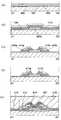
이 실시예에서, 산화물 반도체를 포함하는 반도체 장치를 제작하기 위한 방법이 도 3a 내지 도 3e를 참조하여 기술될 것이다. 이 실시예에서, 결정 영역을 가진 제 1 산화물 반도체층 및 상기 제 1 산화물 반도체층의 상기 결정 영역으로부터의 결정 성장에 의해 형성되는 제 2 산화물 반도체층이 산화물 반도체층으로서 이용되는 반도체 장치를 제작하기 위한 방법, 즉, 도 1b에 도시된 상기 반도체 장치를 제작하기 위한 방법이 상세히 기술될 것이다. 요구된 두께가 상기 제 1 산화물 반도체층에 의해서만 보장될 수 있는 경우에, 상기 제 2 산화물 반도체층은 불필요하다. 탑-게이트형 트랜지스터가 예로서 기술되었지만, 트랜지스터의 구조는 탑-게이트형 구조에 제한되지 않음을 유념한다.In this embodiment, a method for fabricating a semiconductor device including an oxide semiconductor will be described with reference to FIGS. 3A to 3E. In this embodiment, a semiconductor device is fabricated in which a first oxide semiconductor layer having a crystal region and a second oxide semiconductor layer formed by crystal growth from the crystal region of the first oxide semiconductor layer are used as the oxide semiconductor layer. A method for manufacturing, that is, a method for manufacturing the semiconductor device shown in FIG. 1B will be described in detail. If the required thickness can only be ensured by the first oxide semiconductor layer, the second oxide semiconductor layer is unnecessary. Although the top-gate transistor is described as an example, it is noted that the structure of the transistor is not limited to the top-gate structure.
먼저, 상기 절연층(302)은 상기 기판(300) 위에 형성된다. 그 후에, 제 1 산화물 반도체층이 상기 절연층(302) 위에 형성되고, 상기 제 1 산화물 반도체층의 적어도 표면을 포함하는 영역을 결정화하기 위해 제 1 열 처리가 수행되고, 그에 의해 제 1 산화물 반도체층(304)이 형성된다(도 3a 참조).First, the insulating
상기 실시예에서의 상기 기판(200)과 유사한 기판이 상기 기판(300)으로서 이용될 수 있음을 유념한다. 상술된 실시예는 그 상세한 기술에 대해 참조될 수 있다.Note that a substrate similar to the
상기 절연층(302)은 하지의 역할을 하고, 상기 실시예에 기술된 상기 절연층(202)의 방식과 유사한 방식으로 형성될 수 있다. 상술된 실시예는 그 상세한 기술에 대해 참조될 수 있다. 수소 또는 수분을 가능한 적게 함유하도록 상기 절연층(302)을 형성하는 것이 바람직함을 유념한다. 상기 절연층(302)이 제공되지 않는 구조도 또한 이용될 수 있다.The insulating
상기 제 1 산화물 반도체층은 상기 실시예에 기술된 상기 산화물 반도체층(206)의 방식과 유사한 방식으로 형성될 수 있다. 상술된 실시예는 상기 제 1 산화물 반도체층 및 그 형성 방법의 상세들에 대해 참조될 수 있다. 상기 제 1 산화물 반도체층이 이 실시예에서 상기 제 1 열 처리에 의해 의도적으로 결정화되기 때문에, 상기 제 1 산화물 반도체층은 쉽게 결정화되는 산화물 반도체를 이용하여 형성되는 것이 바람직함을 유념한다. 이러한 산화물 반도체로서, 예를 들면 ZnO가 주어질 수 있다. In-Ga-Zn-O계 산화물 반도체의 경우에서도, 예를 들면, 높은 Zn 농도를 가진 것이 쉽게 결정화된다; 금속 원소들(In, Ga 및 Zn) 중에서 Zn의 비율이 60atoms% 이상인 것이 이 목적을 위해 바람직하다. 상기 제 1 산화물 반도체층의 두께는 바람직하게는 1nm 이상 10nm 이하이다. 이 실시예에서, 상기 제 1 산화물 반도체층은 예로서 3nm의 두께를 가진다. 상기 산화물 반도체의 상기 재료, 상기 반도체 장치의 사용 등에 의존하여 적절한 두께가 변하고, 따라서 상기 두께는 상기 재료, 상기 사용 등에 의존하여 적합하게 선택될 수 있음을 유념한다.The first oxide semiconductor layer may be formed in a manner similar to that of the
상기 제 1 열 처리의 온도는 550℃ 이상 850℃ 이하, 바람직하게 600℃ 이상 750℃ 이하이다. 상기 열 처리의 시간은 1분 이상 24시간 이하가 바람직하다. 상기 열 처리의 상기 온도 및 상기 열 처리의 상기 시간은 산화물 반도체의 종류 등에 의존하여 변함을 유념한다.The temperature of the said 1st heat processing is 550 degreeC or more and 850 degrees C or less, Preferably they are 600 degreeC or more and 750 degrees C or less. As for the time of the said heat processing, 1 minute or more and 24 hours or less are preferable. Note that the temperature of the heat treatment and the time of the heat treatment vary depending on the type of oxide semiconductor and the like.
상기 제 1 열 처리가 수행되는 분위기는 수소, 수분 등을 함유하지 않는 것이 바람직하다. 예를 들면, 수분이 충분히 제거된 질소 분위기, 산소 분위기 또는 희가스(헬륨, 네온 또는 아르곤과 같이) 분위기가 이용될 수 있다.It is preferable that the atmosphere in which the first heat treatment is performed does not contain hydrogen, moisture, or the like. For example, a nitrogen atmosphere, an oxygen atmosphere, or a rare gas (such as helium, neon or argon) in which water is sufficiently removed may be used.
상기 열 처리 장치는 반드시 상기 전기로에 제한될 필요가 없고 가열된 가스와 같은 매체로부터 열 복사 또는 열 전도에 의해 가공될 대상을 가열하기 위한 장치일 수 있다. 예를 들면, 램프 급속 열 어닐(LRTA) 장치 또는 가스 급속 열 어닐(GRTA) 장치와 같은 급속 열 어닐(RTA) 장치가 이용될 수 있다. LRTA 장치는 할로겐 램프, 금속 할라이드 램프, 크세논 아크 램프, 탄소 아크 램프, 고압 나트륨 램프, 또는 고압 수은 램프와 같은 램프로부터 방출된 광의 복사(전자파)에 의해 가공될 대상을 가열하기 위한 장치이다. GRTA 장치는 고온 가스를 이용하여 열 처리를 수행하기 위한 장치이다. 상기 가스로서, 질소 또는 아르곤과 같은 희가스와 같이, 열 처리에 의해 가공될 대상과 반응하지 않는 불활성 가스가 이용된다.The heat treatment device does not necessarily need to be limited to the electric furnace and may be a device for heating an object to be processed by heat radiation or heat conduction from a medium such as a heated gas. For example, rapid thermal anneal (RTA) devices such as lamp rapid thermal anneal (LRTA) devices or gas rapid thermal anneal (GRTA) devices can be used. LRTA devices are devices for heating objects to be processed by radiation (electromagnetic waves) of light emitted from lamps such as halogen lamps, metal halide lamps, xenon arc lamps, carbon arc lamps, high pressure sodium lamps, or high pressure mercury lamps. The GRTA apparatus is a apparatus for performing heat treatment using hot gas. As the gas, an inert gas that does not react with the object to be processed by heat treatment, such as a rare gas such as nitrogen or argon, is used.
상기 제 1 열 처리를 통해, 상기 제 1 산화물 반도체층의 적어도 상기 표면을 포함하는 상기 영역이 결정화된다. 상기 결정 영역은 상기 제 1 산화물 반도체층의 상기 표면에서 상기 제 1 산화물 반도체층의 내부쪽으로의 결정 성장에 의해 형성된다. 상기 결정 영역은 일부 경우들에서 1nm 이상 10nm 이하의 평균 두께를 가진 판상 결정을 포함함을 유념한다. 또한, 상기 결정 영역은 상기 제 1 산화물 반도체층의 상기 표면에 실질적으로 평행한 ab 면을 가지고, 일부 경우들에서 상기 표면에 실질적으로 수직인 방향으로 c축 배향된 결정을 포함한다. 여기서, "실질적으로 평행한 방향"은 평행 방향에서 ±10° 내의 방향을 의미하고, "실질적으로 수직인 방향"은 수직 방향에서 ±10° 내의 방향을 의미한다.Through the first heat treatment, the region including at least the surface of the first oxide semiconductor layer is crystallized. The crystal region is formed by crystal growth from the surface of the first oxide semiconductor layer toward the inside of the first oxide semiconductor layer. Note that the crystal region includes in some cases plate crystals having an average thickness of 1 nm or more and 10 nm or less. Further, the crystal region has an ab plane substantially parallel to the surface of the first oxide semiconductor layer, and in some cases includes c-axis oriented crystals in a direction substantially perpendicular to the surface. Here, "substantially parallel direction" means a direction within ± 10 ° in a parallel direction, and "substantially vertical direction" means a direction within ± 10 ° in a vertical direction.
상기 제 1 열 처리를 통해, 상기 결정 영역이 형성되고, 또한, 상기 제 1 산화물 반도체층에서 수소(수분 및 수산기를 포함)가 제거되는 것이 바람직하다. 수소 등이 제거되는 경우에, 상기 제 1 열 처리는 6N(99.9999%) 이상(즉, 불순물들의 농도는 1ppm 이하임)의 순도를 가진, 질소 분위기, 산소 분위기, 또는 희가스(헬륨, 네온 또는 아르곤과 같이) 분위기에서 수행되는 것이 바람직하다. 7N(99.99999%) 이상(즉, 불순물들의 농도는 0.1ppm 이하임)의 순도를 가진 분위기가 더욱 바람직하다. 상기 제 1 산화물 반도체층은 20ppm 이하의 H2O 농도를 가진 초건조 공기, 바람직하게 1ppm 이하의 H2O 농도를 가진 초건조 공기에서 수행될 수 있다.It is preferable that through the first heat treatment, the crystal region is formed, and hydrogen (including water and hydroxyl groups) is removed from the first oxide semiconductor layer. When hydrogen or the like is removed, the first heat treatment is nitrogen, oxygen, or rare gas (helium, neon or argon) with a purity of at least 6N (99.9999%) (i.e. the concentration of impurities is 1 ppm or less). Preferably) in an atmosphere. More preferred is an atmosphere having a purity of 7N (99.99999%) or more (i.e., the concentration of impurities is 0.1 ppm or less). The first oxide semiconductor layer may be performed in the second drying air, preferably with a second H2 O concentration of 1ppm or less dried air with a H2 O concentration of 20ppm or less.
상기 제 1 열 처리를 통해, 상기 결정 영역이 형성되고, 또한, 산소가 상기 제 1 산화물 반도체층에 공급되는 것이 바람직하다. 예를 들면, 상기 열 처리가 수행되는 분위기는 산소 분위기로 설정되고, 그에 의해 산소가 상기 제 1 산화물 반도체층에 공급될 수 있다.It is preferable that the said crystal region is formed through the said 1st heat processing, and oxygen is supplied to the said 1st oxide semiconductor layer. For example, the atmosphere in which the heat treatment is performed is set to an oxygen atmosphere, whereby oxygen can be supplied to the first oxide semiconductor layer.
이 실시예에서, 상기 제 1 열 처리로서, 수소 등이 상기 산화물 반도체층에서 제거되도록 700℃로 1시간 동안 질소 분위기에서 열 처리가 수행된 다음, 상기 질소 분위기는 산소 분위기로 변경된다; 따라서 산소가 상기 제 1 산화물 반도체층에 공급된다. 상기 제 1 열 처리는 결정 영역을 형성하기 위해 주로 수행되어, 수소를 제거하기 위한 처리 또는 산소를 공급하기 위한 처리도 또한 별도로 수행될 수 있다는 것을 유념한다. 예를 들면, 수소를 제거하기 위한 처리 또는 산소를 공급하기 위한 처리가 수행된 후에 결정화를 위한 열 처리를 수행하는 것이 바람직하다.In this embodiment, as the first heat treatment, heat treatment is performed in a nitrogen atmosphere at 700 ° C. for 1 hour so that hydrogen or the like is removed from the oxide semiconductor layer, and then the nitrogen atmosphere is changed to an oxygen atmosphere; Thus, oxygen is supplied to the first oxide semiconductor layer. Note that the first heat treatment is mainly performed to form the crystal region, so that the treatment for removing hydrogen or the treatment for supplying oxygen may also be performed separately. For example, it is preferable to perform a heat treatment for crystallization after a treatment for removing hydrogen or a treatment for supplying oxygen is performed.
이러한 제 1 열 처리를 통해, 상기 결정 영역을 포함하고 수소(수분 및 수산기를 포함) 등이 제거되고 산소가 공급된 상기 제 1 산화물 반도체층(304)이 획득된다.Through this first heat treatment, the first
다음에, 상기 제 2 산화물 반도체층(305)은, 적어도 표면을 포함하는 상기 영역에 상기 결정 영역을 포함하는 상기 제 1 산화물 반도체층(304) 위에 형성된다(도 3b 참조). 요구된 두께가 상기 제 1 산화물 반도체층(304)에 의해서만 보장될 수 있는 경우에, 상기 제 2 산화물 반도체층(305)은 불필요하다. 이 경우, 상기 제 2 산화물 반도체층(305)을 위한 단계들은 생략될 수 있다.Next, the second
상기 제 2 산화물 반도체층(305)은 상기 실시예에 기술된 상기 산화물 반도체층(206)의 방식과 유사한 방식으로 형성될 수 있다. 상술된 실시예는 상기 제 2 산화물 반도체층(305) 및 그 형성 방법의 상세들에 대해 참조될 수 있다. 상기 제 2 산화물 반도체층(305)의 두께는 상기 제 1 산화물 반도체층(304)의 두께보다 큰 것이 바람직함을 유념한다. 상기 제 2 산화물 반도체층(305)은 상기 제 1 산화물 반도체층(304)과 상기 제 2 산화물 반도체층(305)의 두께들의 합이 1nm 이상 50nm 이하, 바람직하게 1nm 이상 10nm 이하가 되도록 형성되는 것이 바람직하다. 이 실시예에서, 상기 제 2 산화물 반도체층(305)은 예를 들면 7nm의 두께를 가진다. 상기 산화물 반도체의 재료, 상기 반도체 장치의 사용 등에 의존하여 적합한 두께가 변하고, 따라서 상기 두께는 상기 재료, 상기 사용 등에 의존하여 적합하게 선택될 수 있음을 유념한다.The second
상기 제 2 산화물 반도체층(305)은 상기 제 1 산화물 반도체층(304)과 동일한 주성분을 함유하고 결정화 후의 격자 상수가 상기 제 1 산화물 반도체층(304)의 격자 상수에 가까운(1% 이하의 미스매치) 재료를 이용하여 형성되는 것이 바람직하다. 이것은 상기 제 1 산화물 반도체층(304)의 상기 결정 영역을 종결정으로 이용한 결정 성장이 상기 제 2 산화물 반도체층(305)의 결정화시 쉽게 진행하기 때문이다. 또한, 상기 제 1 산화물 반도체층(304)과 동일한 주성분을 함유한 상기 재료가 이용되는 경우에, 양호한 계면 특성들 또는 양호한 전기 특성들이 획득될 수 있다.The second
원하는 막 품질이 상기 결정화에 의해 획득되는 경우에, 상기 제 2 산화물 반도체층(305)은 주성분이 상기 제 1 산화물 반도체층(304)의 주성분과 상이한 재료를 이용하여 형성될 수 있음을 유념한다.Note that when the desired film quality is obtained by the crystallization, the second
다음에, 제 2 열 처리는 종(seed)으로서 상기 제 1 산화물 반도체층(304)의 상기 결정 영역을 이용한 결정 성장이 진행하도록 상기 제 2 산화물 반도체층(305)에 대해 수행된다. 이와 같이, 상기 제 2 산화물 반도체층(305)이 형성된다(도 3c 참조). 상기 제 2 산화물 반도체층(305)이 형성되지 않는 경우, 이 구조는 생략될 수 있다.Next, a second heat treatment is performed on the second
상기 제 2 열 처리의 상기 온도는 550℃ 이상 850℃ 이하, 바람직하게 600℃ 이상 750℃ 이하이다. 상기 제 2 열 처리에 대한 시간은 1분 이상 100시간 이하, 바람직하게 5시간 이상 20시간 이하, 통상적으로 10시간이다. 상기 제 2 열 처리가 수행되는 분위기가 수소, 수분 등을 함유하지 않는 것이 바람직함을 유념한다.The temperature of the second heat treatment is at least 550 ° C and at most 850 ° C, preferably at least 600 ° C and at most 750 ° C. The time for the second heat treatment is 1 minute or more and 100 hours or less, preferably 5 hours or more and 20 hours or less, usually 10 hours. Note that the atmosphere in which the second heat treatment is performed does not contain hydrogen, moisture, or the like.
상기 열 처리의 분위기 및 효과의 상세들은 상기 제 1 열 처리와 동일하다. 이용될 수 있는 상기 열 처리 장치는 또한 상기 제 1 열 처리의 경우에서와 동일하다. 예를 들면, 상기 제 2 열 처리에서, 전기로의 내부는 상기 온도가 증가될 때 질소 분위기로 설정되는 반면, 상기 전기로의 내부는 냉각이 수행될 때 산소 분위기로 설정된다; 따라서, 질소 분위기가 이용되는 경우에 수소 등이 제거될 수 있고 산소 분위기가 이용되는 경우에 산소가 공급될 수 있다.Details of the atmosphere and effects of the heat treatment are the same as in the first heat treatment. The heat treatment apparatus that can be used is also the same as in the case of the first heat treatment. For example, in the second heat treatment, the interior of the electric furnace is set to a nitrogen atmosphere when the temperature is increased, while the interior of the electric furnace is set to an oxygen atmosphere when cooling is performed; Therefore, hydrogen or the like can be removed when a nitrogen atmosphere is used and oxygen can be supplied when an oxygen atmosphere is used.
상기 제 2 열 처리는 상기 방식으로 수행되고, 그에 의해 상기 제 1 산화물 반도체층(304)에서 형성된 상기 결정 영역으로부터 상기 제 2 산화물 반도체층(305)의 전체 부분으로 결정 성장이 진행한다; 이와 같이, 상기 제 2 산화물 반도체층(306)이 형성될 수 있다. 수소(수분 및 수산기를 포함) 등이 제거되고 산소가 공급되는 상기 제 2 산화물 반도체층(306)이 형성될 수 있다. 또한, 상기 제 2 열 처리를 통해, 상기 제 1 산화물 반도체층(304)의 상기 결정 영역의 배향을 개선하는 것이 또한 바람직하다.The second heat treatment is performed in the above manner, whereby crystal growth proceeds from the crystal region formed in the first
예를 들면, In-Ga-Zn-O계 산화물 반도체 재료가 상기 제 2 산화물 반도체층(306)에 이용되는 경우에, 상기 제 2 산화물 반도체층(306)은 InGaO3(ZnO)m(m : 정수)에 의해 표현되는 결정, In2Ga2ZnO7(In: Ga: Zn: 0 = 2 : 2 : 1 : 7)에 의해 표현되는 결정 등을 포함할 수 있다. 상기 제 2 열 처리로 인해, 결정과 같은 c-축이 상기 제 2 산화물 반도체층(306)의 표면에 실질적으로 수직인 방향으로 배향된다.For example, when an In—Ga—Zn—O based oxide semiconductor material is used for the second
여기서, 상술된 결정은 In, Ga 및 Zn 중 어느 것을 포함하고, a-축 및 b-축과 평행한 층들의 적층 구조를 가지도록 고려될 수 있다. 특히, 상술된 결정은 In을 함유한 층 및 In을 함유하지 않은 층(Ga 또는 Zn을 함유한 층)이 c-축 방향으로 적층되는 구조를 가진다.Here, the above-described crystal may include any of In, Ga and Zn, and may be considered to have a laminated structure of layers parallel to the a-axis and the b-axis. In particular, the above-described crystal has a structure in which a layer containing In and a layer not containing In (a layer containing Ga or Zn) are laminated in the c-axis direction.
In-Ga-Zn-O계 산화물 반도체 결정에서, 평면 방향, 즉, a-축 및 b-축과 평행한 방향으로 In을 함유한 층의 도전성이 양호하다. 전기 도전성이 주로 상기 In-Ga-Zn-O계 산화물 반도체 결정에서 In에 의해 제어된다는 사실; In 원자 중 하나의 5s 오비탈이 인접한 In 원자의 5s 오비탈과 중첩하는 사실 등으로 인해서, 캐리어 경로가 형성되는 등이다.In the In—Ga—Zn—O based oxide semiconductor crystal, the conductivity of the layer containing In in the plane direction, that is, the direction parallel to the a-axis and the b-axis is good. The fact that electrical conductivity is mainly controlled by In in the In—Ga—Zn—O based oxide semiconductor crystals; Carrier paths are formed due to the fact that the 5s orbital of one In atom overlaps with the 5s orbital of an adjacent In atom.
상기 제 1 산화물 반도체층(304)이 상기 절연층(302)과의 계면에서의 비정질 영역을 포함하는 경우에, 상기 제 2 열 처리가 상기 제 1 산화물 반도체층(304)의 상기 표면 상에 형성된 상기 결정 영역에서 상기 제 1 산화물 반도체층의 하부 표면쪽으로의 결정 성장을 촉진할 수 있고, 일부 경우들에서 상기 비정질 영역을 결정화할 수 있다. 상기 절연층(302)을 형성하기 위한 상기 재료 또는 열 처리 조건들에 의존하여 상기 비정질 영역이 남아있을 수 있음을 유념한다.When the first
상기 제 1 산화물 반도체층(304) 및 상기 제 2 산화물 반도체층(305)이 동일한 주성분을 함유하는 산화물 반도체 재료들을 이용하여 형성되는 경우에, 상기 제 1 산화물 반도체층(304) 및 상기 제 2 산화물 반도체층(306)은 일부 경우들에서 도 3c에 도시된 바와 같이 동일한 결정 구조를 가진다. 따라서, 상기 제 1 산화물 반도체층(304)과 상기 제 2 산화물 반도체층(306) 사이의 경계가 도 3c에 점선에 의해 표시되지만, 이것은 때때로 식별될 수 없고, 상기 제 1 산화물 반도체층(304) 및 상기 제 2 산화물 반도체층(306)이 때때로 하나의 층으로서 간주될 수 있다.When the first
다음에, 상기 제 1 산화물 반도체층(304) 및 상기 제 2 산화물 반도체층(306)은 마스크를 이용한 에칭과 같은 방법에 의해 가공된다; 따라서, 섬형 제 1 산화물 반도체층(304a) 및 섬형 제 2 산화물 반도체층(306a)에 형성된다(도 3d 참조). 여기서, 상기 산화물 반도체층들은 상기 제 2 열 처리 후에 상기 섬형 산화물 반도체층들로 가공되지만, 상기 산화물 반도체층들은 상기 제 2 열 처리 전에 상기 섬형 산화물 반도체층들로 가공될 수 있음을 유념한다. 이 경우, 상기 에칭은 습식 에칭이 이용되는 경우에도 높은 에칭율로 수행될 수 있다; 따라서, 상기 에칭에 요구된 시간이 단축될 수 있다는 이점이 존재한다.Next, the first
상기 제 1 산화물 반도체층(304) 및 상기 제 2 산화물 반도체층(306)을 에칭하기 위한 방법으로서, 건식 에칭 또는 습식 에칭이 이용될 수 있다. 건식 에칭 및 습식 에칭은 조합하여 이용될 수 있음은 말할 필요도 없다. 에칭 조건들(예를 들면, 에칭 가스 또는 에천트, 에칭 시간, 및 온도)은 상기 산화물 반도체층이 원하는 형상으로 에칭될 수 있도록 상기 재료에 의존하여 적합하게 설정된다. 상기 제 1 산화물 반도체층(304) 및 상기 제 2 산화물 반도체층(306)은 상기 실시예에 기술된 상기 산화물 반도체의 방식과 유사한 방식으로 에칭될 수 있다. 상술된 실시예는 그 상세한 기술에 대해 참조될 수 있다.As a method for etching the first
상기 산화물 반도체층에서 채널 형성 영역의 역할을 하는 영역이 평탄화된 표면을 가지는 것이 바람직함을 유념한다. 예를 들면, 상기 제 2 산화물 반도체층(306)의 상기 표면의 피크-투-밸리 간격(P-V)이 상기 게이트 전극(314)(상기 채널 형성 영역)과 중첩하는 영역에서 1nm 이하(바람직하게 0.5nm 이하)가 바람직하다. 상기 피크-투-밸리 간격에 대해, 예를 들면, 10㎛ × 10㎛의 영역에 대해 수행된 측정에 의해 획득된 값이 이용될 수 있음을 유념한다.Note that it is preferable that the region serving as the channel forming region in the oxide semiconductor layer has a flattened surface. For example, the peak-to-valley spacing PV of the surface of the second
다음에, 도전층이 상기 제 2 산화물 반도체층(306a)과 접촉하여 형성된다. 다음에, 상기 도전층은 상기 소스 또는 드레인 전극(308a) 및 상기 소스 또는 드레인 전극(308b)을 형성하기 위해 선택적으로 에칭된다(도 3d 참조). 상기 소스 또는 드레인 전극(308a) 및 상기 소스 또는 드레인 전극(308b)은 상기 실시예에 기술된 상기 소스 또는 드레인 전극(208a) 및 상기 소스 또는 드레인 전극(208b)의 방식과 유사한 방식으로 형성될 수 있다. 상술된 실시예는 그 상세한 기술에 대해 참조될 수 있다.Next, a conductive layer is formed in contact with the second
도 3d의 단계에서, 상기 소스 또는 드레인 전극(308a) 및 상기 소스 또는 드레인 전극(308b)과 접촉한 결정층이 일부 경우들에서 상기 제 1 산화물 반도체층(304a) 또는 상기 제 2 산화물 반도체층(306a)에서 비정질 상태에 있음을 유념한다. 따라서, 상기 제 1 산화물 반도체층(304a) 또는 상기 제 2 산화물 반도체층(306a)의 전체 영역은 반드시 결정 구조를 가질 필요가 없다.In the step of FIG. 3D, the crystalline layer in contact with the source or
다음에, 상기 게이트 절연층(312)은 상기 제 2 산화물 반도체층(306a)의 일부와 접촉하여 형성된다. 상기 게이트 절연층(312)은 상기 실시예에서 상기 게이트 절연층(212)의 방식과 유사한 방식으로 형성될 수 있다. 상술된 실시예는 그 상세한 기술에 대해 참조될 수 있다. 그 후에, 상기 게이트 전극(314)은 상기 게이트 절연층(312) 위에 상기 제 1 산화물 반도체층(304a) 및 상기 제 2 산화물 반도체층(306a)과 중첩하는 영역에서 형성된다. 그 후에, 상기 게이트 절연층(312) 및 상기 게이트 전극(314) 위에 상기 층간 절연층(316) 및 상기 층간 절연층(318)이 형성된다(도 3e 참조). 상기 게이트 전극(314), 상기 층간 절연층(316), 및 상기 층간 절연층(318)은 상기 실시예에 각각 기술된 상기 게이트 전극(214), 상기 층간 절연층(216), 및 상기 층간 절연층(218)의 방식과 유사한 방식으로 형성될 수 있다. 상술된 실시예는 그 상세한 기술에 대해 참조될 수 있다.Next, the
상기 게이트 전극(314)이 형성된 후에, 제 3 열 처리가 불활성 가스 분위기 또는 산소 분위기에서 수행되는 것이 바람직하다. 상기 제 3 열 처리의 온도는 200℃ 이상 450℃ 이하, 바람직하게 250℃ 이상 350℃ 이하이다. 예를 들면, 상기 제 3 열 처리는 250℃로 1시간 동안 산소를 함유한 분위기에서 수행될 수 있다. 상기 제 3 열 처리는 상기 트랜지스터의 전기 특성들의 변동을 감소시킬 수 있다. 상기 게이트 절연층(312)이 산소를 함유한 절연층인 경우에, 산소는 상기 제 2 산화물 절연층(306a)에 공급될 수 있다.After the
상기 제 3 열 처리가 이 실시예에서 상기 게이트 절연층(312)의 형성 후에 수행되지만, 상기 제 3 열 처리의 시간은 이에 제한되지 않음을 유념한다. 상기 제 2 열 처리와 같은 다른 처리에 의해 상기 제 2 산화물 반도체층(306a)에 산소가 공급되는 경우에, 상기 제 3 열 처리가 생략될 수 있다.Note that although the third heat treatment is performed after the formation of the
상기 단계들을 통해, 상기 제 1 산화물 반도체층(304a) 및 상기 제 2 산화물 반도체층(306a)을 포함하는 상기 트랜지스터(350)가 완성된다(도 3e 참조).Through the above steps, the
도 3e에 도시된 상기 트랜지스터(350)는 상기 절연층(302)을 사이에 구비하여 상기 기판(300) 위에 제공된 상기 제 1 산화물 반도체층(304a); 상기 제 1 산화물 반도체층(304a) 위에 제공된 상기 제 2 산화물 반도체층(306a); 상기 제 2 산화물 반도체층(306a)에 전기적으로 접속된 상기 소스 또는 드레인 전극(308a) 및 상기 소스 또는 드레인 전극(308b); 상기 제 2 산화물 반도체층(306a), 상기 소스 또는 드레인 전극(308a), 및 상기 소스 또는 드레인 전극(308b)을 덮도록 제공된 상기 게이트 절연층(312); 상기 게이트 절연층(312) 위의 상기 게이트 전극(314); 상기 게이트 절연층(312) 및 상기 게이트 전극(314) 위의 상기 층간 절연층(316); 및 상기 층간 절연층(316) 위의 상기 층간 절연층(318)을 포함한다.The
이 실시예에서 기술된 상기 트랜지스터(350)에서, 상기 제 1 산화물 반도체층(304a) 및 상기 제 2 산화물 반도체층(306a)이 고순도화되고, 상기 제 1 산화물 반도체층(304a) 및 상기 제 2 산화물 반도체층(306a)의 수소 농도는 5 × 10¹⁹/cm3 이하, 바람직하게 5 × 10¹⁸/cm3 이하, 더욱 바람직하게 5 × 10¹⁷/cm3 이하이다. 상기 제 1 산화물 반도체층(304a) 및 상기 제 2 산화물 반도체층(306a)은 대략 1 × 10¹⁴/cm3의 캐리어 밀도를 가진 일반 실리콘 웨이퍼에 비해, 충분히 낮은 캐리어 밀도(예를 들면, 1 × 10¹²/cm3 미만, 더욱 바람직하게 1.45 × 10¹⁰/cm3 미만)를 가진다. 따라서, 오프 전류가 충분히 감소된다. 예를 들면, 실내 온도에서의 상기 트랜지스터(350)의 오프 전류 밀도(상기 오프 전류가 상기 트랜지스터의 채널 폭으로 나누어지는 방식으로 얻어진 값)는 약 1 × 10-20A/㎛(10zA/㎛) 내지 1 × 10-19A/㎛(100zA/㎛)이다.In the
상기 고순도화되고 진성 산화물 반도체들인 상기 제 1 산화물 반도체층(304a) 및 상기 제 2 산화물 반도체층(306a)의 이용으로, 상기 트랜지스터의 상기 오프 전류가 충분히 감소될 수 있다.By using the first
또한, 이 실시예에서, 상기 결정 영역을 포함하는 상기 제 1 산화물 반도체층(304a) 및 상기 제 1 산화물 반도체층(304a)의 상기 결정 영역으로부터의 결정 성장에 의해 형성되는 상기 제 2 산화물 반도체층(306a)이 상기 산화물 반도체층으로서 이용된다; 따라서, 전계 효과 이동도가 개선되고, 양호한 전기 특성들을 가진 트랜지스터가 실현될 수 있다. 예를 들면, 상기 전계 효과 이동도 μ는 100cm2/V·sec보다 높을 수 있다.Further, in this embodiment, the second oxide semiconductor layer formed by crystal growth from the first
이 실시예에 기술된 바와 같이, 상기 산화물 반도체층 및 상기 게이트 절연층의 두께, 상기 소스 전극과 상기 드레인 전극의 간격 등이 각각의 미리 결정된 범위들에 있고, 그에 의해 양호한 특성들이 유지될 수 있고 소형화가 달성될 수 있다.As described in this embodiment, the thicknesses of the oxide semiconductor layer and the gate insulating layer, the spacing between the source electrode and the drain electrode, and the like are in respective predetermined ranges, whereby good characteristics can be maintained. Miniaturization can be achieved.
이 실시예에 기술된 구조들, 방법들 등은 다른 실시예들에 기술된 구조들, 방법들 등 중 어느 것과 적합하게 조합될 수 있다.The structures, methods, and the like described in this embodiment may be suitably combined with any of the structures, methods, and the like described in other embodiments.
[실시예 4]Example 4
이 실시예에서, 산화물 반도체를 포함하는 반도체 장치를 제작하기 위한 방법이 기술될 것이다. 특히, 도 1c의 상기 반도체 장치를 제작하기 위한 방법이 도 4a 내지 도 4e를 참조하여 기술될 것이다. 이 실시예에 따른 반도체 장치를 제작하기 위한 방법은 상기 실시예들 중 어느 것(특히, 실시예 2)에 기술된 반도체 장치를 제작하기 위한 방법과 공통점을 많이 가짐을 유념한다. 따라서, 상이한 점들이 주로 기술될 것이다. 이 실시예의 제작 방법과 상기 실시예들 중 어느 것(예를 들면, 실시예 3)의 일부와의 조합에 의해 도 1d에 도시된 상기 반도체 장치를 제작하는 것이 가능함을 유념한다.In this embodiment, a method for manufacturing a semiconductor device including an oxide semiconductor will be described. In particular, the method for fabricating the semiconductor device of FIG. 1C will be described with reference to FIGS. 4A-4E. Note that the method for manufacturing the semiconductor device according to this embodiment has much in common with the method for manufacturing the semiconductor device described in any of the above embodiments (particularly, Embodiment 2). Therefore, different points will be mainly described. Note that it is possible to fabricate the semiconductor device shown in FIG. 1D by the combination of the fabrication method of this embodiment and a part of any of the above embodiments (for example, Embodiment 3).
먼저, 상기 절연층(402)은 상기 기판(400) 위에 형성된다. 이후, 산화물 반도체층(406)은 상기 절연층(402) 위에 형성된다(도 4a 참조). 상술된 실시예는 그 상세한 기술에 대해 참조될 수 있다.First, the insulating
다음에, 상기 산화물 반도체층(406)은 상기 섬형 산화물 반도체층(406a)을 형성하기 위해 마스크를 이용한 에칭과 같은 방법에 의해 가공된다. 도전층(408) 및 절연층(410)이 상기 산화물 반도체층(406a)을 덮도록 형성된다(도 4b 참조). 상기 절연층(410)은 필수적인 구성요소가 아니라 나중에 형성될 상기 소스 전극 및 상기 드레인 전극의 측면들을 선택적으로 산화하는데 효과적임을 유념한다. 또한, 상기 절연층(410)은 상기 게이트 전극과 상기 소스 또는 드레인 전극 사이의 커패시턴스를 감소하는데 또한 효과적이다.Next, the
상술된 실시예는 상기 섬형 산화물 반도체층(406a)의 형성 및 열 처리의 상세한 기술에 대해 참조될 수 있다. 그 외에도, 상술된 실시예는 상기 도전층(408)의 상세한 기술에 대해 참조될 수 있다.The above-described embodiment may be referred to for the detailed description of the formation and heat treatment of the island type
상기 절연층(410)은 CVD법, 스퍼터링법 등에 의해 형성될 수 있다. 상기 절연층(410)은 산화 실리콘, 질화 실리콘, 산화질화 실리콘, 산화 알루미늄, 산화 하프늄, 산화 탄탈 등을 함유하도록 형성되는 것이 바람직하다. 상기 절연층(410)은 단층 구조 또는 적층 구조를 가질 수 있음을 유념한다. 상기 절연층(410)의 두께에 대한 특정 제약은 존재하지 않는다; 상기 절연층(410)은 예를 들면 10nm 이상 200nm 이하의 두께를 가질 수 있다.The insulating
다음에, 상기 도전층(408) 및 상기 절연층(410)은 선택적으로 에칭된다; 따라서, 상기 소스 또는 드레인 전극(408a), 상기 소스 또는 드레인 전극(408b), 상기 절연층(410a), 및 상기 절연층(410b)이 형성된다(도 4c 참조). 상세들은 상기 실시예에서의 상기 소스 및 드레인 전극들을 형성하는 공정의 상세들과 유사하다. 알루미늄, 티타늄, 몰리브덴 또는 구리와 같은 재료가 나중에 수행되는 플라즈마 산화 처리에 적합하고, 상기 소스 또는 드레인 전극(408a) 및 상기 소스 또는 드레인 전극(408b)에 대한 재료로서 이용되는 것이 바람직함을 유념한다.Next, the
그 후에, 상기 산화물 반도체층(406a)에 산소를 공급하기 위해 산화 처리가 수행된다. 상기 산화 처리에 의해, 상기 산화물 영역(411a)이 상기 소스 또는 드레인 전극(408a)의 일부에 형성되고, 상기 산화물 영역(411b)이 상기 소스 또는 드레인 전극(408b)의 일부에 형성된다(도 4d 참조). 상기 산화 처리에 의해, 산화물 영역은 또한 상기 소스 또는 드레인 전극(408a) 및 상기 소스 또는 드레인 전극(408b)의 주변부 상에 형성된다.Thereafter, an oxidation process is performed to supply oxygen to the
상기 산화 처리는 마이크로파(300MHz 내지 300GHz)로 여기된 산소 플라즈마를 이용하여 수행되는 것이 바람직하고, 이것은 플라즈마 산화 처리라고 칭해진다. 그 이유는 고밀도 플라즈마가 마이크로파로 플라즈마 여기에 의해 실현되고 상기 산화물 반도체층(406a)에 대한 손상이 충분히 감소될 수 있다는 점이다.The oxidation treatment is preferably performed using an oxygen plasma excited with microwaves (300 MHz to 300 GHz), which is called plasma oxidation treatment. The reason is that high density plasma is realized by plasma excitation with microwaves and damage to the
특히, 상기 처리는 예를 들면 산소와 아르곤의 혼합 가스를 이용하여 200℃ 내지 400℃(통상적으로, 300℃)의 기판 온도에서 50Pa 내지 5000Pa(통상적으로 500Pa)의 압력 하에서 300MHz 내지 300GHz(통상적으로, 2.45GHz)의 주파수로 수행될 수 있다.In particular, the treatment is performed at 300 MHz to 300 GHz (typically under a pressure of 50 Pa to 5000 Pa (typically 500 Pa) at a substrate temperature of 200 ° C. to 400 ° C. (typically 300 ° C.) using a mixed gas of oxygen and argon, for example. , 2.45 GHz).
상기 산화 처리에 의해, 상기 산화물 반도체층(406a)에 산소가 공급된다. 따라서, 상기 산화물 반도체층(406a)에 대한 손상이 충분히 감소될 수 있고, 또한, 산소 결핍으로 인한 에너지 갭의 결함 정도가 감소될 수 있다. 달리 말하면, 상기 산화물 반도체층(406a)의 특성들이 더욱 개선될 수 있다.By the oxidation treatment, oxygen is supplied to the
마이크로파로의 상기 플라즈마 산화 처리에 대한 제약 없이, 상기 산화물 반도체층(406a)에 대한 손상의 충분한 감소 및 상기 산화물 반도체층(406a)으로의 산소의 공급을 가능하게 하는 임의의 다른 방법이 이용될 수 있음을 유념한다. 예를 들면, 산소를 함유한 분위기에서 열 처리와 같은 방법이 이용될 수 있다.Without restriction on the plasma oxidation treatment of microwaves, any other method that allows for a sufficient reduction of damage to the
상기 산화 처리와 조합하여, 상기 산화물 반도체층(406a)으로부터 수분, 수소 등의 제거를 위한 처리가 수행될 수 있다. 이 경우, 예를 들면, 질소 또는 아르곤과 같은 가스를 이용한 플라즈마 처리가 수행될 수 있다.In combination with the oxidation treatment, a treatment for removing moisture, hydrogen, and the like from the
상기 산화 처리에 의해, 상기 산화물 영역(411a) 및 상기 산화물 영역(411b)이 상기 소스 또는 드레인 전극(408a)의 일부 및 상기 소스 또는 드레인 전극(408b)의 일부(특히, 그 측면들에 대응하는 부분들)에 각각 형성됨을 유념한다. 상기 산화물 영역들은 특히 상기 트랜지스터(450)가 소형화될 때(예를 들면, 상기 채널 길이가 1000nm 미만, 특히 70nm 이하일 때) 효과적이다. 상기 트랜지스터의 소형화로, 상기 게이트 절연층(412)이 더 작은 두께를 가져야 한다. 상기 산화물 영역들이 제공되는 이유는 상기 게이트 절연층(412)의 두께의 감소 또는 그것으로의 결함 있는 피복성에 의해 유발될 수 있는 상기 게이트 전극(414)과 상기 소스 또는 드레인 전극(408a) 사이 및 상기 게이트 전극(414)과 상기 소스 또는 드레인 전극(408b) 사이의 단락 회로를 방지할 수 있다는 점이다. 상기 산화물 영역들은 5nm 이상의 두께(특히, 10nm 이상)를 가질 때 충분히 효과적임을 유념한다.By the oxidation treatment, the
상기 산화 처리는 상기 절연층(402)의 노출된 부분의 막 품질의 개선의 관점들에서도 또한 효과적이다.The oxidation treatment is also effective in terms of improving the film quality of the exposed portion of the insulating
상기 절연층(410a) 및 상기 절연층(410b)은, 이들 절연층들이 상기 소스 또는 드레인 전극(408a) 및 상기 소스 또는 드레인 전극(408b)의 상부들의 산화를 방지하는 기능을 한다는 점에서 중요하다는 것을 유념한다. 이것은 에칭에 이용된 마스크가 남아있을 때 상기 플라즈마 처리를 수행하는 것이 상당히 어렵기 때문이다.The insulating
다음에, 상기 게이트 절연층(412)은 대기에 노출되지 않고 상기 산화물 반도체층(406a)의 일부와 접촉하여 형성된다. 그 후에, 상기 게이트 전극(414)은 상기 산화물 반도체층(406a)과 중첩하는 영역에서 상기 게이트 절연층(412) 위에 형성되고, 상기 층간 절연층(416) 및 상기 층간 절연층(418)이 상기 게이트 절연층(412) 및 상기 게이트 절연층(414) 위에 형성된다(도 4e 참조). 상술된 실시예는 그 상세한 기술에 대해 참조될 수 있다.Next, the
상기 단계들을 통해, 산화물 반도체를 포함하는 상기 트랜지스터(450)가 완성된다.Through the above steps, the
이 실시예에서, 산소 플라즈마 처리는 상기 산화물 반도체층(406a)에 산소를 공급하기 위해 상기 산화물 반도체층(406a)에 대해 수행된다. 따라서, 상기 트랜지스터(450)는 더 양호한 특성들을 가진다. 또한, 상기 소스 또는 드레인 전극의 측면에 대응하는 영역이 산화된다; 따라서, 상기 게이트 절연층의 두께의 감소에 의해 유발될 수 있는 상기 게이트 전극과 상기 소스 전극(또는 상기 드레인 전극) 사이의 단락 회로가 방지될 수 있다.In this embodiment, an oxygen plasma treatment is performed on the
또한, 상기 절연층은 상기 소스 및 드레인 전극들 위에 제공될 때, 상기 게이트 전극과 상기 소스 전극 사이 및 상기 게이트 전극과 상기 드레인 전극 사이에 형성된 커패시턴스가 감소될 수 있다; 따라서, 상기 반도체 장치는 더 고속으로 동작할 수 있다.In addition, when the insulating layer is provided over the source and drain electrodes, capacitance formed between the gate electrode and the source electrode and between the gate electrode and the drain electrode can be reduced; Thus, the semiconductor device can operate at higher speed.
이 실시예에 기술된 구조들, 방법들 등은 다른 실시예들에 기술된 구조들, 방법들 등 중 어느 것과 적합하게 조합될 수 있다.The structures, methods, and the like described in this embodiment may be suitably combined with any of the structures, methods, and the like described in other embodiments.
[실시예 5][Example 5]
이 실시예에서, 상기 실시예에 기술된 상기 트랜지스터를 포함하는 반도체 장치의 예가 도 5a 및 도 5b, 도 6a 및 도 6b, 도 7a1, 도 7a2 및 도 7b, 및 도 8a 및 도 8b를 참조하여 기술될 것이다.In this embodiment, an example of a semiconductor device including the transistor described in the above embodiment is described with reference to FIGS. 5A and 5B, 6A and 6B, 7A1, 7A2 and 7B, and 8A and 8B. Will be described.
<반도체 장치의 구조예><Structure Example of Semiconductor Device>
도 5a는 상기 실시예에 기술된 상기 트랜지스터가 다이오드로서 이용되는 경우의 회로 구성을 도시한다. 다이오드-접속된 트랜지스터(110)에서, 제 1 단자 및 게이트 단자측은 양극이고 제 2 단자쪽은 음극임을 유념한다.Fig. 5A shows a circuit configuration when the transistor described in the embodiment is used as a diode. Note that in the diode-connected
도 5b는 n-채널 트랜지스터 및 p-채널 트랜지스터가 상보적으로 조합되는 CMOS 회로의 예를 도시한다. 여기서, 가장 간단한 CMOS 회로인 CMOS 인버터 회로가 기술된다. 상기 CMOS 인버터 회로에서, 제 1 트랜지스터(112)의 게이트 전극이 제 2 트랜지스터(114)의 게이트 전극에 전기적으로 접속되고; 상기 제 1 트랜지스터(112)의 소스 전극은 일 단자 VL에 전기적으로 접속되고; 상기 제 1 트랜지스터(112)의 드레인 전극은 상기 제 2 트랜지스터(114)의 소스 전극에 전기적으로 접속되고; 상기 제 2 트랜지스터(114)의 드레인 전극은 다른 단자 VH에 전기적으로 접속된다.5B shows an example of a CMOS circuit in which an n-channel transistor and a p-channel transistor are complementarily combined. Here, a CMOS inverter circuit which is the simplest CMOS circuit is described. In the CMOS inverter circuit, the gate electrode of the
상기 제 1 트랜지스터(112)는 n-채널 트랜지스터이고, 상기 실시예에 기술된 상기 트랜지스터가 이용될 수 있다. 상기 제 2 트랜지스터(114)는 p-채널 트랜지스터이고, 상기 제 2 트랜지스터(114)는 산화물 반도체 또는 다른 재료들(예를 들면, 실리콘)을 이용하여 형성될 수 있다.The
도 6a는 그 구조가 소위 DRAM(dynamic random access memory)에 대응하는 반도체 장치의 예를 도시한다. 도 6a에 도시된 메모리 셀 어레이(120)는 복수의 메모리 셀들(130)은 매트릭스로 배열되는 구조를 가진다. 상기 메모리 셀 어레이(120)는 복수의 제 1 배선들 및 복수의 제 2 배선들을 포함한다.6A shows an example of a semiconductor device whose structure corresponds to a so-called dynamic random access memory (DRAM). The
상기 메모리 셀(130)은 트랜지스터(131) 및 커패시터(132)를 포함한다. 상기 트랜지스터(131)의 게이트 전극은 상기 제 1 배선에 전기적으로 접속된다. 상기 트랜지스터(131)의 소스 전극 및 드레인 전극 중 하나는 상기 제 2 배선에 전기적으로 접속되고, 상기 트랜지스터(131)의 상기 소스 전극 및 상기 드레인 전극 중 다른 하나는 상기 커패시터의 일 전극에 전기적으로 접속된다. 상기 커패시터의 다른 전극에는 미리 결정된 전위가 공급된다. 상기 실시예들 중 어느 것에 기술된 상기 트랜지스터는 상기 트랜지스터(131)에 적용된다.The
상기 실시예들 중 어느 것에 기술된 상기 트랜지스터는 극히 낮은 오프 전류를 가진다. 따라서, 상기 트랜지스터가 소위 DRAM으로서 인식되는 도 6a에 기술된 상기 반도체 장치에 적용되는 경우에, 실질적으로 비휘발성 메모리가 획득될 수 있다.The transistor described in any of the above embodiments has an extremely low off current. Thus, in the case where the transistor is applied to the semiconductor device described in Fig. 6A, which is recognized as a so-called DRAM, a substantially nonvolatile memory can be obtained.
도 6b는 그 구조가 소위 SRAM(static random access memory)에 대응하는 반도체 장치의 예를 도시한다. 도 6b에 도시된 메모리 셀 어레이(140)가 복수의 메모리 셀들(150)이 매트릭스로 배열되는 구조를 가진다. 상기 메모리 셀 어레이(140)는 복수의 제 1 배선들, 복수의 제 2 배선들, 복수의 제 3 배선들, 및 복수의 제 4 배선들을 포함한다.6B shows an example of a semiconductor device whose structure corresponds to a so-called static random access memory (SRAM). The
상기 메모리 셀(150)은 제 1 트랜지스터(151), 제 2 트랜지스터(152), 제 3 트랜지스터(153), 제 4 트랜지스터(154), 제 5 트랜지스터(155), 및 제 6 트랜지스터(156)를 포함한다. 상기 제 1 트랜지스터(151) 및 상기 제 2 트랜지스터(152) 각각은 선택 트랜지스터로서 기능한다. 상기 제 3 트랜지스터(153) 및 상기 제 4 트랜지스터(154) 중 하나는 n-채널 트랜지스터이고(여기서, 상기 제 4 트랜지스터(154)가 n-채널 트랜지스터이고), 상기 제 3 트랜지스터(153) 및 상기 제 4 트랜지스터(154) 중 다른 하나는 p-채널 트랜지스터이다(여기서, 상기 제 3 트랜지스터(153)가 p-채널 트랜지스터이다). 달리 말하면, 상기 제 3 트랜지스터(153) 및 상기 제 4 트랜지스터(154)는 CMOS 회로를 형성한다. 유사하게, 상기 제 5 트랜지스터(155) 및 상기 제 6 트랜지스터(156)는 CMOS 회로를 형성한다.The
상기 제 1 트랜지스터(151), 상기 제 2 트랜지스터(152), 상기 제 4 트랜지스터(154) 및 상기 제 6 트랜지스터(156)는 n-채널 트랜지스터들이고, 상기 실시예들 중 어느 것에 기술된 상기 트랜지스터는 이에 적용될 수 있다. 상기 제 3 트랜지스터(153) 및 상기 제 5 트랜지스터(155)는 p-채널 트랜지스터들이고, 이들은 산화물 반도체 또는 다른 재료들(예를 들면, 실리콘)을 이용하여 형성될 수 있다.The
<비휘발성 메모리 장치의 구조예><Structure Example of Nonvolatile Memory Device>
다음에, 상기 실시예들 중 어느 것에 따른 상기 트랜지스터를 포함하는 비휘발성 메모리 장치의 구조예가 도 7a1, 도 7a2 및 도 7b 및 도 8a 및 도 8b를 참조하여 기술될 것이다.Next, a structural example of a nonvolatile memory device including the transistor according to any of the above embodiments will be described with reference to FIGS. 7A1, 7A2 and 7B and 8A and 8B.
도 7a1에 도시된 반도체 장치에서, 제 1 배선(제 1 선, 또한 소스선이라고도 칭해짐) 및 트랜지스터(160)의 소스 전극이 서로 전기적으로 접속되고, 제 2 배선(제 2 선, 또한 비트선이라고도 칭해짐) 및 상기 트랜지스터(160)의 드레인 전극이 서로 전기적으로 접속된다. 제 3 배선(제 3 선, 또한 제 1 신호선이라고도 칭해짐) 및 트랜지스터(162)의 소스 전극 및 드레인 전극 중 하나가 서로 전기적으로 접속된다. 제 4 배선(제 4 선, 또한 제 2 신호선이라고도 칭해짐) 및 트랜지스터(162)의 게이트 전극이 서로 전기적으로 접속된다. 상기 트랜지스터(160)의 게이트 전극 및 상기 트랜지스터(162)의 상기 소스 전극 및 상기 드레인 전극이 상기 커패시터(164)의 일 전극에 전기적으로 접속되고, 제 5 배선(제 5 선, 또한 워드선이라고도 칭해짐) 및 상기 커패시터(164)의 다른 전극이 서로 전기적으로 접속된다.In the semiconductor device shown in FIG. 7A1, a first wiring (a first line, also referred to as a source line) and a source electrode of the
여기서, 상기 실시예들 중 어느 것에 기술된 산화물 반도체를 포함하는 상기 트랜지스터가 적어도 상기 트랜지스터(162)에 적용된다. 상기 실시예들 중 어느 것에 기술된 산화물 반도체를 포함하는 상기 트랜지스터가 극히 낮은 오프 전류를 가진다. 이러한 이유로, 상기 트랜지스터(160)의 상기 게이트 전극의 전위는 상기 트랜지스터(162)를 턴 오프함으로써 극히 장시간 동안 유지될 수 있다. 상기 커패시터(164)가 제공되고, 이것은 상기 트랜지스터(160)의 상기 게이트 전극에 주어진 전하의 유지 및 저장된 데이터의 판독을 용이하게 한다. 산화물 반도체를 포함하는 상기 트랜지스터(162)는 10nm 이상 1000nm 이하, 예를 들면 10nm 이상 70nm 이하의 채널 길이(L)를 가진다; 따라서, 이것은 저전력 소비 및 고속 동작의 특성들을 가진다. 상기 트랜지스터(160)는 산화물 반도체 또는 다른 재료들을 포함할 수 있다.Here, the transistor including the oxide semiconductor described in any of the above embodiments is applied to at least the
도 7a1에 도시된 상기 반도체 장치는 상기 트랜지스터(160)의 상기 게이트 전극의 전위가 유지되고, 그에 의해 데이터의 기록, 유지, 및 판독이 하기에 기술된 바와 같이 수행될 수 있는 이점을 활용한다.The semiconductor device shown in FIG. 7A1 takes advantage of the potential that the potential of the gate electrode of the
먼저, 데이터의 기록 및 유지에 관한 기술이 이루어진다. 먼저, 상기 제 4 배선의 전위는 상기 트랜지스터(162)가 턴 온되는 전위로 설정되어, 상기 트랜지스터(162)가 턴 온된다. 따라서, 상기 제 3 배선의 전위는 상기 트랜지스터(160)의 상기 게이트 전극 및 상기 커패시터(164)에 공급된다. 즉, 미리 결정된 전하가 상기 트랜지스터(160)의 상기 게이트 전극에 주어진다(기록). 여기서, 2개의 상이한 전위들(이후, 로우-레벨 전하 및 하이-레벨 전하라고 칭해짐)의 공급을 위한 전하들 중 하나가 상기 트랜지스터(160)의 상기 게이트 전극에 주어진다. 그 후, 상기 제 4 배선의 상기 전위는 상기 트랜지스터(162)가 턴 오프되는 전위로 설정되어, 상기 트랜지스터(162)는 턴 오프된다. 따라서, 상기 트랜지스터(160)의 상기 게이트 전극에 주어진 전하가 유지된다(홀딩).First, a technique relating to recording and holding of data is made. First, the potential of the fourth wiring is set to a potential at which the
상기 트랜지스터(162)의 상기 오프 전류가 상당히 작기 때문에, 상기 트랜지스터(160)의 상기 게이트 전극의 전하가 장시간 동안 유지된다.Since the off current of the
다음에, 데이터의 판독에 관한 기술이 이루어진다. 미리 결정된 전위(정전위)가 상기 제 1 배선에 공급되는 동안 상기 제 5 배선에 적합한 전위(판독 전위)를 공급함으로써, 상기 제 2 배선의 상기 전위는 상기 트랜지스터(160)의 상기 게이트 전극에 유지된 전하량에 의존하여 변한다. 이것은 일반적으로, 상기 트랜지스터(160)가 n-채널 트랜지스터일 때, 하이-레벨 전하가 상기 트랜지스터(160)의 상기 게이트 전극에 주어지는 경우의 피상 임계 전압 Vth_H는 로우-레벨 전하가 상기 트랜지스터(160)의 상기 게이트 전극에 주어지는 경우의 피상 임계 전압 Vth_L보다 낮기 때문이다. 여기서, 피상 임계 전압은 상기 제 5 배선의 상기 전위를 나타내며, 이것은 상기 트랜지스터(160)를 턴 온하는데 필요하다. 따라서, 상기 제 5 배선의 상기 전위는 Vth_H와 Vth_L 사이의 중간 전위 V0으로 설정되고, 그에 의해 상기 트랜지스터(160)의 상기 게이트 전극에 주어진 전하가 결정될 수 있다. 예를 들면, 하이-레벨 전하가 기록에 주어지는 경우에, 상기 제 5 배선의 상기 전위가 V0(> Vth_H)으로 설정될 때, 상기 트랜지스터(160)가 턴 온된다. 로우-레벨 전하가 기록에 주어지는 경우에, 상기 제 5 배선의 상기 전위가 V0(< Vth_L)으로 설정될 때에도, 상기 트랜지스터(160)는 오프 상태에 남아있다. 따라서, 저장된 데이터는 상기 제 2 배선의 상기 전위에 의해 판독될 수 있다.Next, a description regarding the reading of data is made. By supplying a potential (reading potential) suitable for the fifth wiring while a predetermined potential (static potential) is supplied to the first wiring, the potential of the second wiring is held at the gate electrode of the
데이터가 판독되지 않는 경우에, 상기 트랜지스터(160)가 상기 게이트 전극의 상태에 상관 없이 턴 오프되도록 허용하는 전위, 즉 Vth_H보다 낮은 전위가 상기 제 5 배선에 적용될 수 있다. 대안적으로, 상기 트랜지스터(160)가 상기 게이트 전극의 상태에 상관 없이 턴 온되도록 허용하는 전위, 즉 Vth_L보다 높은 전위가 상기 제 5 배선에 적용될 수 있다.In the case where data is not read, a potential that allows the
그 후에, 데이터의 재기록에 관한 기술이 이루어진다. 데이터의 재기록은 데이터의 기록 및 유지의 방식과 유사한 방식으로 수행된다. 즉, 상기 제 4 배선의 상기 전위는 상기 트랜지스터(162)를 턴 온하도록 허용하는 전위로 설정되고, 그에 의해 상기 트랜지스터(162)가 턴 온 된다. 따라서, 상기 제 3 배선의 전위(새로운 데이터에 관련된 전위)가 상기 트랜지스터(160)의 상기 게이트 전극 및 상기 커패시터(164)에 공급된다. 그 후에, 상기 제 4 배선의 상기 전위는 상기 트랜지스터(162)가 턴 오프되도록 허용하는 전위로 설정되고, 그에 의해 상기 트랜지스터(162)가 턴 오프된다. 따라서, 새로운 데이터에 관련된 전하가 상기 트랜지스터(160)의 상기 게이트 전극에 주어진다.Thereafter, a description regarding the rewriting of data is made. Rewriting of data is performed in a manner similar to that of recording and maintaining data. That is, the potential of the fourth wiring is set to a potential that allows the
개시된 발명에 따른 상기 반도체 장치에서, 상술된 바와 같이 데이터의 다른 기록에 의해 데이터가 직접 재기록될 수 있다. 그러한 이유로, 플래시 메모리 등에 필요한 소거 동작은 요구되지 않으므로, 상기 소거 동작에 의해 유발되는 동작 속도의 감소가 방지될 수 있다. 달리 말하면, 상기 반도체 장치의 고속 동작이 실현될 수 있다.In the semiconductor device according to the disclosed invention, the data can be directly rewritten by another writing of the data as described above. For that reason, an erase operation required for a flash memory or the like is not required, so that a decrease in the operation speed caused by the erase operation can be prevented. In other words, the high speed operation of the semiconductor device can be realized.
상기 트랜지스터(162)의 상기 소스 전극 또는 상기 드레인 전극은 상기 트랜지스터(160)의 상기 게이트 전극에 전기적으로 접속되고, 그에 의해 비휘발성 메모리 소자에 이용되는 플로팅 게이트 트랜지스터의 플로팅 게이트의 효과와 유사한 효과를 가짐을 유념한다. 따라서, 상기 트랜지스터(162)의 상기 소스 전극 또는 상기 드레인 전극이 상기 트랜지스터(160)의 상기 게이트 전극에 전기적으로 접속되는 도면에서의 부분은 일부 경우들에서 플로팅 게이트부 FG라고 칭해진다. 상기 트랜지스터(162)가 오프될 때, 상기 플로팅 게이트부 FG는 절연체에 임베딩되는 것으로 간주될 수 있고 따라서 전하가 상기 플로팅 게이트부 FG에 유지된다. 산화물 반도체를 포함하는 상기 트랜지스터(162)의 오프 전류량은 실리콘 반도체 등을 포함하는 트랜지스터의 오프 전류량 이하 내지 이의 십만 분의 일 이하이다; 따라서, 상기 트랜지스터(162)의 누설 전류로 인한 상기 플로팅 게이트부 FG에 축적된 전하의 손실은 무시할 수 있다. 즉, 산화물 반도체를 포함하는 상기 트랜지스터(162)로, 비휘발성 메모리 장치가 실현될 수 있다.The source electrode or the drain electrode of the
도 7a1에 도시된 상기 반도체 장치는, 도 7a1에서의 상기 반도체 장치의 트랜지스터와 같은 구성요소들이 저항 및 커패시터를 포함한다고 가정한 도 7a2에 도시된 회로 구조를 가질 수 있다. 즉, 도 7a2에서, 상기 트랜지스터(160) 및 상기 커패시터(164)는 저항 및 커패시터를 포함하는 것으로 각각 간주된다. R1 및 C1은 상기 커패시터(164)의 저항값 및 커패시턴스 값을 각각 표시한다. 상기 저항값 R1은 상기 커패시터(164)에 포함된 절연층에 의존하는 저항값에 대응한다. R2 및 C2는 상기 커패시터(160)의 저항값 및 커패시턴스 값을 각각 표시한다. 상기 저항값 R2는 상기 커패시터(160)가 온일 때의 게이트 절연층에 의존하는 저항값에 대응한다. 상기 커패시턴스 값 C2는 소위 게이트 커패시턴스(상기 게이트 전극과 상기 소스 전극 또는 상기 드레인 전극 사이에 형성된 커패시턴스)의 커패시턴스 값에 대응한다. 상기 저항값 R2는 상기 트랜지스터(160)의 상기 게이트 전극과 그 채널 형성 영역 사이의 저항값을 도시할 뿐이고, 접속 부분은 이 부분을 명확하게 보여주기 위해 점선으로 도시됨을 유념한다.The semiconductor device shown in FIG. 7A1 may have the circuit structure shown in FIG. 7A2 assuming that components such as transistors of the semiconductor device in FIG. 7A1 include a resistor and a capacitor. That is, in FIG. 7A2, the
상기 트랜지스터(162)가 오프 상태에 있는 경우에 상기 소스 전극과 상기 드레인 전극 사이의 상기 저항값(또한 유효 저항이라고도 칭해짐)이 ROS일 때 및 ROS가 R1 이하이거나 ROS가 R2 이하일 때, 전하 유지 기간(또한 데이터 유지 기간이라고도 칭해짐)은 상기 트랜지스터(162)의 오프 전류에 의해 주로 결정된다.Charge retention when the resistance value (also referred to as an effective resistance) between the source electrode and the drain electrode is ROS when the
한편, 상기 조건들이 충족되지 않을 때, 상기 트랜지스터(162)의 상기 오프 전류가 충분히 작을 때에도 상기 유지 기간을 충분히 보장하기가 어렵다. 이것은, 상기 트랜지스터(162) 이외의 부분에서 유발되는 누설이 크기 때문이다. 따라서, 이 실시예에 개시된 상기 반도체 장치가 상기 관계식을 만족하는 것이 바람직하다고 말할 수 있다.On the other hand, when the conditions are not satisfied, it is difficult to sufficiently ensure the sustain period even when the off current of the
C1 ≥ C2가 만족되는 것이 바람직하다. C1이 큰 경우, 상기 제 5 배선의 상기 전위는 상기 플로팅 게이트부 FG의 상기 전위가 상기 제 5 배선에 의해 제어될 때(예를 들면, 판독시) 낮게 유지될 수 있다.It is preferable that C1 ≧ C2 is satisfied. When C1 is large, the potential of the fifth wiring can be kept low when the potential of the floating gate portion FG is controlled by the fifth wiring (for example, when reading).
상기 관계식이 만족될 때, 더욱 바람직한 반도체 장치가 실현될 수 있다. R1 및 R2는 상기 트랜지스터(160)의 상기 게이트 절연층 및 상기 트랜지스터(162)의 게이트 절연층에 의해 제어됨을 유념한다. 동일한 관계식이 C1 및 C2에 적용된다. 따라서, 상기 게이트 절연층의 재료, 두께 등이 상기 관계식을 만족하기 위해 적합하게 설정되는 것이 바람직하다.When the above relation is satisfied, a more preferable semiconductor device can be realized. Note that R1 and R2 are controlled by the gate insulating layer of the
상기 반도체 장치와 상이한 구조를 가진 반도체 장치가 도 7b에 도시된다. 도 7b에 도시된 상기 반도체 장치에서, 상기 트랜지스터(160)의 상기 게이트 전극, 상기 트랜지스터(162)의 상기 소스 전극 및 상기 드레인 전극 중 하나, 및 상기 커패시터(164)의 일 전극이 서로 전기적으로 접속된다. 상기 트랜지스터(160)의 상기 소스 전극 및 상기 제 1 배선이 서로 전기적으로 접속된다. 상기 트랜지스터(160)의 상기 드레인 전극 및 상기 제 2 배선이 서로 전기적으로 접속된다. 상기 트랜지스터(162)의 상기 소스 전극 및 상기 드레인 전극 중 다른 하나와 상기 제 3 배선이 서로 전기적으로 접속된다. 상기 트랜지스터(162)의 제 1 게이트 전극과 상기 제 4 배선이 서로 전기적으로 접속된다. 상기 커패시터(164)의 다른 전극 및 상기 제 5 배선이 서로 전기적으로 접속된다. 상기 트랜지스터(162)의 제 2 게이트 전극 및 상기 제 6 배선이 서로 전기적으로 접속된다. 상기 제 4 배선에 인가된 것과 동일한 전위가 상기 제 6 배선에 인가될 수 있다. 대안적으로, 상기 제 6 배선이 상기 제 4 배선과 무관하게 제어되도록, 상기 제 4 배선에 인가된 것과 상이한 전위가 상기 제 6 배선에 인가될 수 있다.A semiconductor device having a structure different from that of the semiconductor device is shown in Fig. 7B. In the semiconductor device shown in FIG. 7B, the gate electrode of the
즉, 도 7b에서의 상기 반도체 장치에서, 도 7a1의 상기 반도체 장치의 상기 트랜지스터(162)는 상기 제 2 게이트 전극을 가진 상기 트랜지스터(162)와 대체된다. 따라서, 도 7b의 상기 반도체 장치는 도 7a1의 상기 반도체 장치에서 획득된 효과들 외에도, 상기 트랜지스터(162)의 전기 특성들(예를 들면, 상기 임계 전압)을 쉽게 조정하는 효과를 획득할 수 있다. 예를 들면, 상기 제 6 배선에 음의 전위의 인가에 의해, 상기 트랜지스터(162)는 용이하게 정상-오프될 수 있다.That is, in the semiconductor device of FIG. 7B, the
전자들이 다수 캐리어들인 n-채널 트랜지스터가 상기 기술에 이용되고; 정공들이 다수 캐리어들인 p-채널 트랜지스터가 상기 n-채널 트랜지스터 대신에 이용될 수 있음은 말할 필요가 없음을 유념한다.N-channel transistors in which electrons are majority carriers are used in the technique; Note that a p-channel transistor in which holes are multiple carriers can be used instead of the n-channel transistor.
다음에, 도 7a1, 도 7a2 및 도 7b에 도시된 상기 반도체 장치들의 응용예들이 도 8a 및 도 8b를 참조하여 기술된다. 도 8a 및 도 8b는 도 7a1에 도시된 복수의 반도체 장치들(이후, 또한 메모리 셀들(190)이라고도 칭해짐)을 각각 포함하는 반도체 장치들의 회로도들의 예들이다. 도 8a는 상기 메모리 셀들(190)이 직렬로 접속된 소위 NAND 반도체 장치의 회로도이고, 도 8b는 상기 메모리 셀들(190)이 병렬로 접속되는 소위 NOR 반도체 장치의 회로도이다.Next, applications of the semiconductor devices shown in FIGS. 7A1, 7A2, and 7B are described with reference to FIGS. 8A and 8B. 8A and 8B are examples of circuit diagrams of semiconductor devices each including a plurality of semiconductor devices (hereinafter also referred to as memory cells 190) shown in FIG. 7A1. 8A is a circuit diagram of a so-called NAND semiconductor device in which the
도 8a의 상기 반도체 장치는 소스선 SL, 비트선 BL, 제 1 신호선 S1, 복수의 제 2 신호선들 S2, 복수의 워드선들 WL, 및 상기 복수의 메모리 셀들(190)을 포함한다. 도 8a에서, 하나의 소스선 SL 및 하나의 비트선 BL이 상기 반도체 장치에 제공된다; 그러나, 개시된 발명의 일 실시예는 이에 제한되지 않는다. 복수의 소스선들 SL 및 복수의 비트선들 BL이 제공될 수 있다.The semiconductor device of FIG. 8A includes a source line SL, a bit line BL, a first signal line S1, a plurality of second signal lines S2, a plurality of word lines WL, and the plurality of
상기 메모리 셀들(190)의 각각에서, 상기 트랜지스터(160)의 상기 게이트 전극, 상기 트랜지스터(162)의 상기 소스 전극 및 상기 드레인 전극 중 하나, 및 상기 커패시터(164)의 일 전극이 서로 전기적으로 접속된다. 상기 제 1 신호선 S1 및 상기 트랜지스터(162)의 상기 소스 전극과 상기 드레인 전극 중 다른 하나가 서로 전기적으로 접속되고, 상기 제 2 신호선 S2와 상기 트랜지스터(162)의 상기 게이트 전극이 서로 전기적으로 접속된다. 상기 워드선 WL 및 상기 커패시터(164)의 다른 전극이 서로 전기적으로 접속된다.In each of the
또한, 상기 메모리 셀(190)에 포함된 상기 트랜지스터(160)의 상기 소스 전극은 인접한 메모리 셀(190)에서의 상기 트랜지스터(160)의 상기 드레인 전극에 전기적으로 접속된다. 상기 메모리 셀(190)에 포함된 상기 트랜지스터(160)의 상기 드레인 전극은 상기 인접한 메모리 셀(190)에서의 상기 트랜지스터(160)의 상기 소스 전극에 전기적으로 접속된다. 단부들 중 하나에 제공되는 직렬로 접속된 상기 복수의 메모리 셀들의 상기 메모리 셀(190)에 포함된 상기 트랜지스터(160)의 상기 드레인 전극은 상기 비트선에 전기적으로 접속됨을 유념한다. 다른 단부에 제공되는 직렬로 접속된 상기 복수의 메모리 셀들의 상기 메모리 셀(190)에 포함된 상기 트랜지스터(160)의 상기 소스 전극은 상기 소스선에 전기적으로 접속된다.In addition, the source electrode of the
도 8a에서의 상기 반도체 장치에서, 기록 동작 및 판독 동작이 각각의 로우에서 수행된다. 상기 기록 동작은 다음과 같이 수행된다. 상기 트랜지스터(162)가 턴 온되는 전위가 기록이 수행되는 로우의 상기 제 2 신호선 S2에 공급되어, 기록이 수행되는 상기 로우의 상기 트랜지스터(162)가 턴 온된다. 따라서, 상기 제 1 신호선 S1의 전위는 특정 로우의 상기 트랜지스터(160)의 상기 게이트 전극에 공급되어, 미리 결정된 전하가 상기 게이트 전극에 주어진다. 따라서, 데이터가 상기 특정 로우의 상기 메모리 셀에 기록될 수 있다.In the semiconductor device in Fig. 8A, a write operation and a read operation are performed in each row. The write operation is performed as follows. A potential at which the
또한, 판독 동작이 다음과 같이 수행된다. 먼저, 상기 트랜지스터(160)가 그 게이트 전극의 전하에 상관 없이 턴 온되는 전위가 판독이 수행되는 로우 이외의 로우들의 상기 워드선들 WL에 공급되어, 판독이 수행되는 상기 로우 이외의 로우들의 상기 트랜지스터들(160)이 턴 온된다. 그 후에, 상기 트랜지스터(160)의 온 상태 또는 오프 상태가 상기 트랜지스터(160)의 상기 게이트 전극의 전하에 의존하여 결정되는 전위(판독 전위)가 판독이 수행되는 상기 로우의 상기 워드선 WL에 공급된다. 그 후에, 상기 비트선 BL에 접속된 판독 회로(도시되지 않음)가 동작되도록 정전위가 상기 소스선 SL에 공급된다. 여기서, 상기 소스선 SL과 상기 비트선 BL 사이의 상기 복수의 트랜지스터들(160)은 판독이 수행되는 상기 로우의 상기 트랜지스터들(160)에 제외된다; 따라서, 상기 소스선 SL과 상기 비트선 BL 사이의 컨덕턴스는 판독이 수행되는 상기 로우의 상기 트랜지스터들(160)의 상태에 의해 결정된다. 즉, 판독 회로에 의해 판독되는 상기 비트선 BL의 전위는 판독이 수행되는 상기 로우의 상기 트랜지스터들(160)의 상기 게이트 전극의 전하에 의존한다. 이러한 방식으로, 데이터가 특정 메모리 셀로부터 판독될 수 있다.Also, the read operation is performed as follows. First, a potential at which the
도 8b의 상기 반도체 장치는 복수의 소스선들 SL, 복수의 비트선들 BL, 복수의 제 1 신호선들 S1, 복수의 제 2 신호선들 S2, 복수의 워드선들 SL 및 복수의 상기 메모리 셀들(190)을 포함한다. 상기 트랜지스터(160)의 상기 게이트 전극, 상기 트랜지스터(162)의 상기 소스 전극 및 상기 드레인 전극 중 하나, 및 상기 커패시터(164)의 일 전극이 서로 전기적으로 접속된다. 상기 소스선 SL 및 상기 트랜지스터(160)의 상기 소스 전극이 서로 전기적으로 접속된다. 상기 비트선 BL 및 상기 트랜지스터(160)의 상기 드레인 전극이 서로 전기적으로 접속된다. 상기 제 1 신호선 S1 및 상기 트랜지스터(162)의 상기 소스 전극과 상기 드레인 전극 중 다른 하나가 서로 전기적으로 접속되고, 상기 제 2 신호선 S2와 상기 트랜지스터(162)의 상기 게이트 전극이 서로 전기적으로 접속된다. 상기 워드선 WL 및 상기 커패시터(164)의 다른 전극이 서로 전기적으로 접속된다.The semiconductor device of FIG. 8B includes a plurality of source lines SL, a plurality of bit lines BL, a plurality of first signal lines S1, a plurality of second signal lines S2, a plurality of word lines SL, and a plurality of
도 8b의 상기 반도체 장치에서, 기록 동작 및 판독 동작이 각각의 로우에서 수행된다. 상기 기록 동작은 도 8a의 상기 반도체 장치의 방식과 유사한 방식으로 수행된다. 상기 판독 동작은 다음과 같이 수행된다. 먼저, 상기 트랜지스터(160)가 그 게이트 전극의 전하에 상관 없이 턴 오프되는 전위가 판독이 수행되는 로우 이외의 로우들의 상기 워드선들 WL에 공급되어, 판독이 수행되는 상기 로우 이외의 로우들의 상기 트랜지스터들(160)이 턴 오프된다. 그 후에, 상기 트랜지스터(160)의 온 상태 또는 오프 상태가 상기 트랜지스터(160)의 상기 게이트 전극의 전하에 의존하여 결정되는 전위(판독 전위)가 판독이 수행되는 상기 로우의 상기 워드선 WL에 공급된다. 그 후에, 상기 비트선 BL에 접속된 판독 회로(도시되지 않음)가 동작되도록 정전위가 상기 소스선 SL에 공급된다. 여기서, 상기 소스선 SL과 상기 비트선 BL 사이의 컨덕턴스는 판독이 수행되는 상기 로우의 상기 트랜지스터들(160)의 상태에 의해 결정된다. 즉, 판독 회로에 의해 판독되는 상기 비트선 BL의 전위는 판독이 수행되는 상기 로우의 상기 트랜지스터들(160)의 상기 게이트 전극의 전하에 의존한다. 이러한 방식으로, 데이터가 특정 메모리 셀로부터 판독될 수 있다.In the semiconductor device of Fig. 8B, a write operation and a read operation are performed in each row. The write operation is performed in a manner similar to that of the semiconductor device of FIG. 8A. The read operation is performed as follows. First, a potential at which the
이 실시예에 기술된 구조들, 방법들 등은 다른 실시예들에 기술된 구조들, 방법들 등 중 어느 것과 적합하게 조합될 수 있다.The structures, methods, and the like described in this embodiment may be suitably combined with any of the structures, methods, and the like described in other embodiments.
[실시예 6][Example 6]
이 실시예에서, 상기 실시예들 중 어느 것에 기술된 상기 반도체 장치가 전자 장치에 적용되는 경우는 도 9a 내지 도 9f를 참조하여 기술될 것이다. 이 실시예에서, 상기 반도체 장치가 컴퓨터, 모바일 폰 핸드세트(또한 모바일 폰 또는 모바일 폰 장치라고도 칭해짐), 개인 휴대 정보 단말(휴대용 게임기, 오디오 재생 장치 등을 포함), 디지털 카메라 또는 디지털 비디오 카메라와 같은 카메라, 전자 페이퍼 및 텔레비전 장치(또한 텔레비전 또는 텔레비전 수신기라고도 칭해짐)와 같은 전자 장치들에 적용되는 경우가 기술된다.In this embodiment, the case where the semiconductor device described in any of the above embodiments is applied to an electronic device will be described with reference to Figs. 9A to 9F. In this embodiment, the semiconductor device is a computer, a mobile phone handset (also referred to as a mobile phone or a mobile phone device), a personal digital assistant (including handheld game consoles, audio playback devices, etc.), digital cameras or digital video cameras. The case is applied to electronic devices such as cameras, electronic papers, and television devices (also referred to as televisions or television receivers).
도 9a는 하우징(601), 하우징(602), 표시부(603), 키보드(604) 등을 포함하는 노트북 개인용 컴퓨터를 도시한다. 상기 하우징(601) 및 상기 하우징(602)에서, 상기 실시예들 중 어느 것에 기술된 상기 반도체 장치가 제공된다. 따라서, 소형, 고속 동작, 및 저전력 소비의 특성들을 가진 노트북 개인용 컴퓨터가 실현될 수 있다.9A illustrates a notebook personal computer including a
도 9b는 표시부(613)가 구비된 본체(611), 외부 인터페이스(615), 조작 버튼들(614) 등을 포함하는 개인 휴대 정보 단말(PDA)을 도시한다. 또한, 상기 개인 휴대 정보 단말 등을 제어하는 스타일러스(612)가 제공된다. 상기 본체(611)에는, 상기 실시예들 중 어느 것에 기술된 상기 반도체 장치가 제공된다. 따라서, 소형, 고속 동작, 및 저전력 소비의 특성들을 가진 개인 휴대 정보 단말이 실현될 수 있다.FIG. 9B illustrates a personal digital assistant (PDA) including a
도 9c는 전자 페이퍼가 장착되고 2개의 하우징들, 하우징(621) 및 하우징(623)을 포함하는 전자 서적(620)을 도시한다. 상기 하우징(621) 및 상기 하우징(623)에는 각각 표시부(625) 및 표시부(627)가 구비된다. 상기 하우징(621)은 축부(637)에 의해 상기 하우징(623)과 결합되어, 상기 전자 서적(620)은 축으로서 상기 축부(637)를 이용하여 개폐될 수 있다. 상기 하우징(621)에는 전력 버튼(631), 조작 키들(633), 스피커(635) 등이 구비된다. 상기 하우징(621) 및 상기 하우징(623) 중 적어도 하나에서, 상기 실시예들 중 어느 것에 기술된 상기 반도체 장치가 제공된다. 따라서, 소형, 고속 동작, 및 저전력 소비의 특성들을 가진 전자 서적이 실현될 수 있다.9C shows an
도 9d는 2개의 하우징들, 하우징(640) 및 하우징(641)을 포함하는 모바일 폰을 도시한다. 또한, 도 9d에 도시된 바와 같이 개발된 상태에서 상기 하우징들(640 및 641)은 하나가 다른 하나와 겹쳐지도록 슬라이딩될 수 있다. 따라서, 상기 모바일 폰의 크기가 감소될 수 있고, 이것은 상기 모바일 폰을 주변에서 휴대하기 적합하게 한다. 상기 하우징(641)은 표시 패널(642), 스피커(643), 마이크로폰(644), 포인팅 디바이스(646), 카메라 렌즈(647), 외부 접속 단자(648) 등을 포함한다. 상기 하우징(640)은 상기 모바일 폰을 충전하기 위한 태양 전지(649), 외부 메모리 슬롯(650) 등을 포함한다. 그 외에도, 안테나가 상기 하우징(641)에 일체화된다. 상기 하우징들(640 및 641) 중 적어도 하나에서, 상기 실시예들 중 어느 것에 기술된 상기 반도체 장치가 제공된다. 따라서, 소형, 고속 동작, 및 저전력 소비의 특성들을 가진 모바일 폰이 실현될 수 있다.9D shows a mobile phone comprising two housings, a
도 9e는 본체(661), 표시부(667), 접안부(663), 조작 스위칭(664), 표시부(665), 배터리(666) 등을 포함하는 디지털 카메라를 도시한다. 상기 본체(661)에는, 상기 실시예들 중 어느 것에 기술된 상기 반도체 장치가 제공된다. 따라서, 소형, 고속 동작, 및 저전력 소비의 특성들을 가진 디지털 카메라가 실현될 수 있다.9E shows a digital camera including a
도 9f는 하우징(671), 표시부(673), 스탠드(675) 등을 포함하는 텔레비전 장치(670)를 도시한다. 상기 텔레비전 장치(670)는 하우징(671)의 조작 스위치 또는 원격 제어기(680)로 조작될 수 있다. 상기 하우징(671) 및 상기 원격 제어기(680)에는 상기 실시예들 중 어느 것에 기술된 상기 반도체 장치가 장착된다. 따라서, 고속 동작 및 저전력 소비의 특성들을 가진 텔레비전 장치가 실현될 수 있다.9F shows a
상술된 바와 같이, 이 실시예에 기술된 상기 전자 장치들은 상기 실시예들 중 어느 것에 따른 상기 반도체 장치가 각각 장착된다. 따라서, 소형, 고속 동작, 및 저전력 소비의 특성들을 가진 전자 장치가 실현될 수 있다.As described above, the electronic devices described in this embodiment are each equipped with the semiconductor device according to any of the embodiments. Thus, an electronic device having characteristics of small size, high speed operation, and low power consumption can be realized.
개시된 발명에 따른 트랜지스터를 이용하여, 쇼트-채널 효과가 충분히 억제된 반도체 장치가 실현될 수 있다. 컴퓨터 시뮬레이션에 의해 효과를 확인한 결과들이 도 10a 내지 도 10c, 도 11, 및 도 12를 참조하여 기술될 것이다.By using the transistor according to the disclosed invention, a semiconductor device in which the short-channel effect is sufficiently suppressed can be realized. The results of confirming the effect by computer simulation will be described with reference to FIGS. 10A to 10C, 11, and 12.
이 예의 컴퓨터 시뮬레이션에서, 그 구조가 도 1a의 구조에 대응하는 트랜지스터가 모델로서 이용되었다. 산화물 반도체층에서, 대역 갭은 3.15eV이었고, 비유전율이 15이었고, 전자 이동도가 10cm2/V·s이었음이 가정되었다. 소스 또는 드레인 전극의 전자 친화력 및 상기 산화물 반도체층의 전자 친화력은 서로 동일하다고(4.3eV) 가정되었다. 게이트 전극은 텅스텐층으로 가정되었고, 그 일함수는 4.6eV라고 가정되었다. Silvaco Data Systems Inc.에 의해 제작된 장치 시뮬레이터 "Atlas"가 계산에 이용되었다.In the computer simulation of this example, a transistor whose structure corresponds to that of FIG. 1A was used as a model. In the oxide semiconductor layer, it was assumed that the band gap was 3.15 eV, the relative dielectric constant was 15, and the electron mobility was 10 cm2 / V · s. It is assumed that the electron affinity of the source or drain electrode and the electron affinity of the oxide semiconductor layer are the same (4.3 eV). The gate electrode was assumed to be a tungsten layer and its work function was assumed to be 4.6 eV. The device simulator "Atlas" manufactured by Silvaco Data Systems Inc. was used for the calculation.
상기 계산에 따른 파라미터들로서, 상기 산화물 반도체층의 두께(tos), 게이트 절연층의 두께(d), 상기 트랜지스터의 임계 전압(Vth), 상기 트랜지스터의 채널 길이(L) 등이 이용되었다. 도 10a 내지 도 10c는 계산 결과들을 도시한다. 도 10a 내지 도 10c에서, 수평축은 상기 채널 길이 L(nm)을 표현하고, 수직 축은 상기 임계 전압 Vth을 표현한다. 도 10a 내지 도 10c에서, 상기 게이트 절연층들의 4개의 상이한 두께들에 대한 상기 채널 길이 L과 상기 임계 전압 Vth 사이의 관계가 도시된다.As parameters according to the calculation, a thickness tos of the oxide semiconductor layer, a thickness d of the gate insulating layer, a threshold voltage Vth of the transistor, a channel length L of the transistor, and the like are used. 10A-10C show the calculation results. 10A-10C, the horizontal axis represents the channel length L (nm) and the vertical axis represents the threshold voltage Vth . 10A-10C, the relationship between the channel length L and the threshold voltage Vth for four different thicknesses of the gate insulating layers is shown.
도 11에 상기 도시된 결과들로부터, 정상-오프 트랜지스터를 실현할 필요가 있는 상기 채널 길이 L(nm)의 하한이 계산될 수 있다. 도 11에서, 상기 산화물 반도체층의 상기 두께(tos)와 상기 게이트 절연층의 상기 두께(d) 사이의 관계에서, 정상-오프 트랜지스터를 실현할 필요가 있는 상기 채널 길이 L(nm)의 하한이 도시된다. 도 11에서, 상기 수평축은 비유전율 εr이 상기 게이트 절연층의 상기 두께(d)로 나누어지는 방식으로 얻어진 값(nm-1)을 표현하고, 상기 수직축은 상기 채널 길이의 허용 가능한 하한 Lmin(nm)을 표현한다. 정상-오프 트랜지스터를 실현하기 위한 조건으로서, Vth > 0이 이용되었음을 유념한다. 즉, 도 11은 상기 산화물 반도체층의 상기 두께(tos)와 상기 게이트 절연층의 상기 두께(d) 사이의 상기 관계를 고려하여 도 10a 내지 도 10c에서 Vth > 0을 만족하는 상기 채널 길이 L의 상기 하한의 플롯을 도시한다. 도면에서 곡선들은 근사선들임을 유념한다.From the results shown above in Fig. 11, the lower limit of the channel length L (nm) that needs to be realized for the normal-off transistor can be calculated. In Fig. 11, in the relation between the thickness tos of the oxide semiconductor layer and the thickness d of the gate insulating layer, the lower limit of the channel length L (nm) that needs to be realized for the normal-off transistor is shown. do. In FIG. 11, the horizontal axis represents a value (nm−1 ) obtained in such a manner that a relative dielectric constant εr is divided by the thickness d of the gate insulating layer, and the vertical axis is an allowable lower limit Lmin of the channel length. express (nm). Note that Vth > 0 was used as a condition for realizing the normal-off transistor. That is, FIG. 11 illustrates the channel length L satisfying Vth > 0 in FIGS. 10A to 10C in consideration of the relationship between the thickness tos of the oxide semiconductor layer and the thickness d of the gate insulating layer. Plot of the lower limit of. Note that the curves in the figures are approximations.
도 11로부터, tos가 30nm인 경우에, 상기 채널 길이 L은 εr/d가 1.3(nm-1) 이상 7.9(nm-1) 이하에 있을 때 20(nm) 이상 70(nm) 이하의 범위에 있음을 알았다. tos가 10nm인 경우에, 상기 채널 길이 L은 εr/d가 1.3(nm-1) 이상 7.9(nm-1) 이하에 있을 때 15(nm) 이상 40(nm) 이하의 범위에 있다. tos가 3nm인 경우에, 상기 채널 길이 L은 εr/d가 1.3(nm-1) 이상 7.9(nm-1) 이하에 있을 때 10(nm) 이상 30(nm) 이하의 범위에 있다.11, when tos is 30 nm, the channel length L is in the range of 20 (nm) or more and 70 (nm) or less when εr / d is 1.3 (nm-1 ) or more and 7.9 (nm-1 ) or less. Found out. When tos is 10 nm, the channel length L is in the range of 15 (nm) or more and 40 (nm) or less when εr / d is 1.3 (nm−1 ) or more and 7.9 (nm−1 ). When tos is 3 nm, the channel length L is in the range of 10 (nm) to 30 (nm) when εr / d is 1.3 (nm-1 ) or more and 7.9 (nm-1 ) or less.
이것은 tos가 3(nm) 이상 30(nm) 이하이고, εr/d가 1.3(nm-1) 이상 7.9(nm-1) 이하에 있을 경우, 상기 채널 길이 L이 10(nm) 이상 70(nm) 이하임을 보여준다.This means that when the tos is 3 (nm) or more and 30 (nm) or less and εr / d is 1.3 (nm-1 ) or more and 7.9 (nm-1 ), the channel length L is 10 (nm) or more and 70 ( nm) or less.
도 12는 개시된 발명에 따른 트랜지스터의 스위칭 속도(스위칭 주파수)와 그 채널 길이 L 사이의 관계를 도시한다. 도 12에서, 상기 수평축은 상기 채널 길이 L(nm)을 표현하고, 상기 수직축은 상기 스위칭 속도(GHz)를 표현한다. 여기서, 상기 스위칭 속도는 상기 스위칭에 요구된 시간의 역수 τ이다.12 shows the relationship between the switching speed (switching frequency) and its channel length L of a transistor according to the disclosed invention. In FIG. 12, the horizontal axis represents the channel length L (nm), and the vertical axis represents the switching speed (GHz). Here, the switching speed is the inverse τ of the time required for the switching.
예를 들면, 상기 채널 길이 L이 10(nm) 이상 70(nm) 이하일 때, 1/τ가 1(GHz) 이상 20(GHz) 이하인 고속 동작이 실현될 수 있음을 이해한다.For example, when the channel length L is 10 (nm) or more and 70 (nm) or less, it is understood that high speed operation with 1 / τ of 1 (GHz) or more and 20 (GHz) or less can be realized.
이 출원은 2009년 12월 25일 일본 특허청에 출원된 일본 특허 출원 일련번호 제2009-294738호에 기초하며, 그 전체 내용들은 본 명세서에 참조로서 포함된다.This application is based on Japanese Patent Application Serial No. 2009-294738 filed with the Japan Patent Office on December 25, 2009, the entire contents of which are incorporated herein by reference.
110 : 트랜지스터112 : 트랜지스터
114 : 트랜지스터120 : 메모리 셀 어레이
130 : 메모리 셀131 : 트랜지스터
132 : 커패시터140 : 메모리 셀 어레이
150 : 메모리 셀
151, 152, 153, 154, 155, 156, 160, 162 : 트랜지스터
164 : 커패시터190 : 메모리 셀
200 : 기판202 : 절연층
206 : 산화물 반도체층206a : 산화물 반도체층
208a : 소스 또는 드레인 전극208b : 소스 또는 드레인 전극
212 : 게이트 절연층214 : 게이트 전극
216, 218 : 층간 절연층218 : 층간 절연층
250 : 트랜지스터300 : 기판
302 : 절연층304 : 산화물 반도체층
304a : 산화물 반도체층305 : 산화물 반도체층
306 : 산화물 반도체층306a : 산화물 반도체층
308a : 소스 또는 드레인 전극308b : 소스 또는 드레인 전극
312 : 게이트 절연층314 : 게이트 전극
316 : 층간 절연층318 : 층간 절연층
350 : 트랜지스터400 : 기판
402 : 절연층406 : 산화물 반도체층
406a : 산화물 반도체층408 : 도전층
408a : 소스 또는 드레인 전극408b : 소스 또는 드레인 전극
410 : 절연층410a : 절연층
410b : 절연층411a : 산화물 영역
411b : 산화물 영역412 : 게이트 절연층
414 : 게이트 전극416 : 층간 절연층
418 : 층간 절연층450 : 트랜지스터
500 : 기판502 : 절연층
504a : 산화물 반도체층506a : 산화물 반도체층
508a : 소스 또는 드레인 전극508b : 소스 또는 드레인 전극
510a : 절연층510b : 절연층
511a : 산화물 영역511b : 산화물 영역
512 : 게이트 절연층514 : 게이트 전극
516 : 층간 절연층518 : 층간 절연층
550 : 트랜지스터601 : 하우징
602 : 하우징603 : 표시부
604 : 키보드611 : 본체
612 : 스타일러스613 : 표시부
614 : 조작 버튼615 : 외부 인터페이스
620 : 전자 서적621 : 하우징
623 : 하우징625 : 표시부
627 : 표시부631 : 전력 버튼
633 : 조작 키635 : 스피커
637 : 축부640 : 하우징
641 : 하우징642 : 표시 패널
643 : 스피커644 : 마이크로폰
646 : 포인팅 디바이스647 : 카메라 렌즈
648 : 외부 접속 단자649 : 태양 전지 셀
650 : 외부 메모리 슬롯661 : 본체
663 : 접안부664 : 조작 스위치
665 : 표시부666 : 배터리
667 : 표시부670 : 텔레비전 장치
671 : 하우징673 : 표시부
675 : 스탠드680 : 원격 제어기110: transistor 112: transistor
114: transistor 120: memory cell array
130: memory cell 131: transistor
132: capacitor 140: memory cell array
150: memory cell
151, 152, 153, 154, 155, 156, 160, 162: transistor
164
200: substrate 202: insulating layer
206:
208a: source or
212: gate insulating layer 214: gate electrode
216, 218: interlayer insulating layer 218: interlayer insulating layer
250: transistor 300: substrate
302: insulating layer 304: oxide semiconductor layer
304a: oxide semiconductor layer 305: oxide semiconductor layer
306:
308a: source or
312: gate insulating layer 314: gate electrode
316: interlayer insulation layer 318: interlayer insulation layer
350: transistor 400: substrate
402: insulating layer 406: oxide semiconductor layer
406a: oxide semiconductor layer 408: conductive layer
408a: source or
410: insulating
410b: insulating
411b: oxide region 412: gate insulating layer
414: gate electrode 416: interlayer insulating layer
418: interlayer insulating layer 450: transistor
500
504a:
508a: source or
510a:
511a:
512: gate insulating layer 514: gate electrode
516: Interlayer insulating layer 518: Interlayer insulating layer
550
602: housing 603: display
604: keyboard 611: main body
612: Stylus 613: display unit
614: operation button 615: external interface
620: eBook 621: housing
623: housing 625: display unit
627: display unit 631: power button
633: operation keys 635: speaker
637: shaft portion 640: housing
641
643: speaker 644: microphone
646: pointing device 647: camera lens
648: external connection terminal 649: solar cell
650: external memory slot 661: main body
663 eyepiece 664: operation switch
665: display unit 666: battery
667: display unit 670: television device
671: housing 673: display unit
675 stand 680 remote control
Claims (3)
Translated fromKorean기판 위에 산화물 반도체층을 형성하는 제 1 공정과;
상기 산화물 반도체층과 전기적으로 접속되는 소스 전극 및 드레인 전극을 형성하는 제 2 공정과;
300MHz 이상 300GHz 이하의 고주파 전력 및 산소와 아르곤의 혼합 가스를 사용한 플라즈마 처리를 수행함으로써 상기 소스 전극 및 상기 드레인 전극의 측면을 산화시키는 제 3 공정과;
상기 제 3 공정을 수행한 후, 상기 산화물 반도체층, 상기 소스 전극 및 상기 드레인 전극을 덮는 게이트 절연층을 형성하는 제 4 공정과;
상기 게이트 절연층 위에 게이트 전극을 형성하는 제 5 공정을 갖는, 반도체 장치 제작 방법.In the semiconductor device manufacturing method,
A first step of forming an oxide semiconductor layer on the substrate;
A second step of forming a source electrode and a drain electrode electrically connected to the oxide semiconductor layer;
A third step of oxidizing side surfaces of the source electrode and the drain electrode by performing plasma treatment using a high frequency power of 300 MHz or more and 300 GHz or less and a mixed gas of oxygen and argon;
A fourth step of forming a gate insulating layer covering the oxide semiconductor layer, the source electrode and the drain electrode after performing the third step;
And a fifth step of forming a gate electrode on said gate insulating layer.
상기 플라즈마 처리를 수행함으로써 상기 산화물 반도체층에 산소를 공급하는, 반도체 장치 제작 방법.The method of claim 1,
And supplying oxygen to the oxide semiconductor layer by performing the plasma treatment.
상기 제 3 공정을 수행하기 전에, 상기 산화물 반도체층의 수소를 저감시키는 처리를 수행하는, 반도체 장치 제작 방법.
3. The method according to claim 1 or 2,
Before the third process, a process of reducing hydrogen in the oxide semiconductor layer is performed.
Applications Claiming Priority (3)
| Application Number | Priority Date | Filing Date | Title |
|---|---|---|---|
| JPJP-P-2009-294738 | 2009-12-25 | ||
| JP2009294738 | 2009-12-25 | ||
| PCT/JP2010/072185WO2011077966A1 (en) | 2009-12-25 | 2010-12-03 | Semiconductor device and method for manufacturing the same |
Related Parent Applications (1)
| Application Number | Title | Priority Date | Filing Date |
|---|---|---|---|
| KR1020127019545ADivisionKR101811203B1 (en) | 2009-12-25 | 2010-12-03 | Semiconductor device and method for manufacturing the same |
Publications (2)
| Publication Number | Publication Date |
|---|---|
| KR20130054469A KR20130054469A (en) | 2013-05-24 |
| KR101301463B1true KR101301463B1 (en) | 2013-08-29 |
Family
ID=44186319
Family Applications (4)
| Application Number | Title | Priority Date | Filing Date |
|---|---|---|---|
| KR1020197007447AExpired - Fee RelatedKR102111309B1 (en) | 2009-12-25 | 2010-12-03 | Method for manufacturing semiconductor device |
| KR1020127019545AExpired - Fee RelatedKR101811203B1 (en) | 2009-12-25 | 2010-12-03 | Semiconductor device and method for manufacturing the same |
| KR1020177036007ACeasedKR20170142998A (en) | 2009-12-25 | 2010-12-03 | Method for manufacturing semiconductor device |
| KR1020137012009AExpired - Fee RelatedKR101301463B1 (en) | 2009-12-25 | 2010-12-03 | Semiconductor device and method for manufacturing the same |
Family Applications Before (3)
| Application Number | Title | Priority Date | Filing Date |
|---|---|---|---|
| KR1020197007447AExpired - Fee RelatedKR102111309B1 (en) | 2009-12-25 | 2010-12-03 | Method for manufacturing semiconductor device |
| KR1020127019545AExpired - Fee RelatedKR101811203B1 (en) | 2009-12-25 | 2010-12-03 | Semiconductor device and method for manufacturing the same |
| KR1020177036007ACeasedKR20170142998A (en) | 2009-12-25 | 2010-12-03 | Method for manufacturing semiconductor device |
Country Status (5)
| Country | Link |
|---|---|
| US (3) | US8664652B2 (en) |
| JP (4) | JP5079076B2 (en) |
| KR (4) | KR102111309B1 (en) |
| TW (3) | TWI608622B (en) |
| WO (1) | WO2011077966A1 (en) |
Families Citing this family (44)
| Publication number | Priority date | Publication date | Assignee | Title |
|---|---|---|---|---|
| KR20190093706A (en) | 2010-01-24 | 2019-08-09 | 가부시키가이샤 한도오따이 에네루기 켄큐쇼 | Display device and manufacturing method thereof |
| KR101932576B1 (en) | 2010-09-13 | 2018-12-26 | 가부시키가이샤 한도오따이 에네루기 켄큐쇼 | Semiconductor device and method for manufacturing the same |
| KR101995682B1 (en)* | 2011-03-18 | 2019-07-02 | 가부시키가이샤 한도오따이 에네루기 켄큐쇼 | Oxide semiconductor film, semiconductor device, and manufacturing method of semiconductor device |
| US9130044B2 (en) | 2011-07-01 | 2015-09-08 | Semiconductor Energy Laboratory Co., Ltd. | Semiconductor device and manufacturing method thereof |
| KR102014876B1 (en) | 2011-07-08 | 2019-08-27 | 가부시키가이샤 한도오따이 에네루기 켄큐쇼 | Semiconductor device and method for manufacturing the same |
| KR102089505B1 (en)* | 2011-09-23 | 2020-03-16 | 가부시키가이샤 한도오따이 에네루기 켄큐쇼 | Semiconductor device |
| US9018629B2 (en)* | 2011-10-13 | 2015-04-28 | Semiconductor Energy Laboratory Co., Ltd. | Semiconductor device and method for manufacturing semiconductor device |
| WO2013054933A1 (en)* | 2011-10-14 | 2013-04-18 | Semiconductor Energy Laboratory Co., Ltd. | Semiconductor device |
| TWI483344B (en) | 2011-11-28 | 2015-05-01 | Au Optronics Corp | Array substrate and manufacturing method thereof |
| TWI621185B (en) | 2011-12-01 | 2018-04-11 | 半導體能源研究所股份有限公司 | Semiconductor device and method of manufacturing semiconductor device |
| EP2786404A4 (en) | 2011-12-02 | 2015-07-15 | Semiconductor Energy Lab | SEMICONDUCTOR DEVICE AND METHOD FOR MANUFACTURING THE SAME |
| JP6053490B2 (en) | 2011-12-23 | 2016-12-27 | 株式会社半導体エネルギー研究所 | Method for manufacturing semiconductor device |
| WO2013094547A1 (en) | 2011-12-23 | 2013-06-27 | Semiconductor Energy Laboratory Co., Ltd. | Semiconductor device and method for manufacturing the same |
| KR101308809B1 (en) | 2012-01-20 | 2013-09-13 | 경희대학교 산학협력단 | Fabrication method of oxide semiconductor thin film transistor and display devices and sensor device applying it |
| TWI463670B (en)* | 2012-03-28 | 2014-12-01 | E Ink Holdings Inc | Active component |
| JP6224931B2 (en) | 2012-07-27 | 2017-11-01 | 株式会社半導体エネルギー研究所 | Semiconductor device |
| JP6059501B2 (en) | 2012-10-17 | 2017-01-11 | 株式会社半導体エネルギー研究所 | Method for manufacturing semiconductor device |
| JP6021586B2 (en) | 2012-10-17 | 2016-11-09 | 株式会社半導体エネルギー研究所 | Semiconductor device |
| JP2014082388A (en) | 2012-10-17 | 2014-05-08 | Semiconductor Energy Lab Co Ltd | Semiconductor device |
| JP6204145B2 (en) | 2012-10-23 | 2017-09-27 | 株式会社半導体エネルギー研究所 | Semiconductor device |
| WO2014065343A1 (en) | 2012-10-24 | 2014-05-01 | Semiconductor Energy Laboratory Co., Ltd. | Semiconductor device |
| US9569992B2 (en) | 2012-11-15 | 2017-02-14 | Semiconductor Energy Laboratory Co., Ltd. | Method for driving information processing device, program, and information processing device |
| TWI620323B (en)* | 2012-11-16 | 2018-04-01 | 半導體能源研究所股份有限公司 | Semiconductor device |
| JP6376788B2 (en)* | 2013-03-26 | 2018-08-22 | 株式会社半導体エネルギー研究所 | Semiconductor device and manufacturing method thereof |
| KR102537022B1 (en)* | 2013-05-20 | 2023-05-30 | 가부시키가이샤 한도오따이 에네루기 켄큐쇼 | Semiconductor device |
| TWI664731B (en)* | 2013-05-20 | 2019-07-01 | 半導體能源研究所股份有限公司 | Semiconductor device |
| CN109888022A (en)* | 2013-05-20 | 2019-06-14 | 株式会社半导体能源研究所 | semiconductor device |
| KR102290801B1 (en)* | 2013-06-21 | 2021-08-17 | 가부시키가이샤 한도오따이 에네루기 켄큐쇼 | Semiconductor device and manufacturing method thereof |
| WO2015114476A1 (en) | 2014-01-28 | 2015-08-06 | Semiconductor Energy Laboratory Co., Ltd. | Semiconductor device |
| JP2015188062A (en) | 2014-02-07 | 2015-10-29 | 株式会社半導体エネルギー研究所 | semiconductor device |
| WO2015145292A1 (en) | 2014-03-28 | 2015-10-01 | Semiconductor Energy Laboratory Co., Ltd. | Transistor and semiconductor device |
| US10109707B2 (en)* | 2014-03-31 | 2018-10-23 | Flosfia Inc. | Crystalline multilayer oxide thin films structure in semiconductor device |
| US10090388B2 (en)* | 2014-03-31 | 2018-10-02 | Flosfia Inc. | Crystalline multilayer structure and semiconductor device |
| JPWO2015151337A1 (en)* | 2014-03-31 | 2017-04-13 | 株式会社東芝 | THIN FILM TRANSISTOR, SEMICONDUCTOR DEVICE, AND METHOD FOR MANUFACTURING THIN FILM TRANSISTOR |
| US9780226B2 (en)* | 2014-04-25 | 2017-10-03 | Semiconductor Energy Laboratory Co., Ltd. | Semiconductor device and manufacturing method thereof |
| US9954113B2 (en) | 2015-02-09 | 2018-04-24 | Semiconductor Energy Laboratory Co., Ltd. | Transistor including oxide semiconductor, semiconductor device including the transistor, and electronic device including the transistor |
| JP6887243B2 (en) | 2015-12-11 | 2021-06-16 | 株式会社半導体エネルギー研究所 | Transistors, semiconductor devices, electronic devices and semi-conducting wafers |
| JP6839986B2 (en) | 2016-01-20 | 2021-03-10 | 株式会社半導体エネルギー研究所 | Manufacturing method of semiconductor device |
| US9852801B1 (en)* | 2016-12-01 | 2017-12-26 | Commissariat A L'energie Atomique Et Aux Energies Alternatives | Method for determining a leakage current through an inter-gate dielectric structure of a flash memory cell |
| JP2018170324A (en) | 2017-03-29 | 2018-11-01 | 株式会社ジャパンディスプレイ | Display device |
| JP2018170325A (en) | 2017-03-29 | 2018-11-01 | 株式会社ジャパンディスプレイ | Display device |
| JP2019129281A (en) | 2018-01-26 | 2019-08-01 | 株式会社ジャパンディスプレイ | Display device and method of manufacturing the same |
| KR102553773B1 (en)* | 2019-01-09 | 2023-07-11 | 어플라이드 머티어리얼스, 인코포레이티드 | Methods of Forming Structures in Semiconductor Devices |
| KR20220134639A (en)* | 2020-02-07 | 2022-10-05 | 가부시키가이샤 플로스피아 | Semiconductor devices and semiconductor devices |
Citations (4)
| Publication number | Priority date | Publication date | Assignee | Title |
|---|---|---|---|---|
| KR20020014201A (en)* | 2000-08-17 | 2002-02-25 | 김효근 | Method of plasma treatment for enhancing ohmic contact characteristics of ZnO semiconductor |
| US20050056826A1 (en)* | 2002-03-20 | 2005-03-17 | Joerg Appenzeller | Self-aligned nanotube field effect transistor and method of fabricating same |
| KR20080053355A (en)* | 2005-09-06 | 2008-06-12 | 캐논 가부시끼가이샤 | A field effect transistor using an amorphous oxide film as a channel layer, a method of manufacturing a field effect transistor using an amorphous oxide film as a channel layer, and a method of manufacturing an amorphous oxide film |
| KR20080076747A (en)* | 2007-02-16 | 2008-08-20 | 삼성전자주식회사 | Oxide semiconductor layer formation method and semiconductor device manufacturing method using the same |
Family Cites Families (136)
| Publication number | Priority date | Publication date | Assignee | Title |
|---|---|---|---|---|
| US4335161A (en)* | 1980-11-03 | 1982-06-15 | Xerox Corporation | Thin film transistors, thin film transistor arrays, and a process for preparing the same |
| JPS60198861A (en) | 1984-03-23 | 1985-10-08 | Fujitsu Ltd | Thin film transistor |
| JPH0244256B2 (en) | 1987-01-28 | 1990-10-03 | Kagaku Gijutsucho Mukizaishitsu Kenkyushocho | INGAZN2O5DESHIMESARERUROTSUHOSHOKEINOSOJOKOZOOJUSURUKAGOBUTSUOYOBISONOSEIZOHO |
| JPS63210023A (en) | 1987-02-24 | 1988-08-31 | Natl Inst For Res In Inorg Mater | Compound having a hexagonal layered structure represented by InGaZn↓4O↓7 and its manufacturing method |
| JPH0244260B2 (en) | 1987-02-24 | 1990-10-03 | Kagaku Gijutsucho Mukizaishitsu Kenkyushocho | INGAZN5O8DESHIMESARERUROTSUHOSHOKEINOSOJOKOZOOJUSURUKAGOBUTSUOYOBISONOSEIZOHO |
| JPH0244258B2 (en) | 1987-02-24 | 1990-10-03 | Kagaku Gijutsucho Mukizaishitsu Kenkyushocho | INGAZN3O6DESHIMESARERUROTSUHOSHOKEINOSOJOKOZOOJUSURUKAGOBUTSUOYOBISONOSEIZOHO |
| JPH0244262B2 (en) | 1987-02-27 | 1990-10-03 | Kagaku Gijutsucho Mukizaishitsu Kenkyushocho | INGAZN6O9DESHIMESARERUROTSUHOSHOKEINOSOJOKOZOOJUSURUKAGOBUTSUOYOBISONOSEIZOHO |
| JPH0244263B2 (en) | 1987-04-22 | 1990-10-03 | Kagaku Gijutsucho Mukizaishitsu Kenkyushocho | INGAZN7O10DESHIMESARERUROTSUHOSHOKEINOSOJOKOZOOJUSURUKAGOBUTSUOYOBISONOSEIZOHO |
| JPH03101556A (en) | 1989-09-14 | 1991-04-26 | Fujitsu Ltd | Isdn protocol test system |
| JPH03101556U (en)* | 1990-02-05 | 1991-10-23 | ||
| EP0445535B1 (en) | 1990-02-06 | 1995-02-01 | Sel Semiconductor Energy Laboratory Co., Ltd. | Method of forming an oxide film |
| JPH05251705A (en) | 1992-03-04 | 1993-09-28 | Fuji Xerox Co Ltd | Thin-film transistor |
| JP3181692B2 (en)* | 1992-06-26 | 2001-07-03 | 富士通株式会社 | Thin film transistor and method of manufacturing the same |
| JP3479375B2 (en) | 1995-03-27 | 2003-12-15 | 科学技術振興事業団 | Metal oxide semiconductor device in which a pn junction is formed with a thin film transistor made of a metal oxide semiconductor such as cuprous oxide, and methods for manufacturing the same |
| JP3591061B2 (en)* | 1995-06-13 | 2004-11-17 | カシオ計算機株式会社 | Method for manufacturing thin film transistor |
| KR100394896B1 (en) | 1995-08-03 | 2003-11-28 | 코닌클리케 필립스 일렉트로닉스 엔.브이. | A semiconductor device including a transparent switching element |
| US5847410A (en) | 1995-11-24 | 1998-12-08 | Semiconductor Energy Laboratory Co. | Semiconductor electro-optical device |
| JP3625598B2 (en) | 1995-12-30 | 2005-03-02 | 三星電子株式会社 | Manufacturing method of liquid crystal display device |
| JP4170454B2 (en) | 1998-07-24 | 2008-10-22 | Hoya株式会社 | Article having transparent conductive oxide thin film and method for producing the same |
| JP3837935B2 (en)* | 1998-09-16 | 2006-10-25 | セイコーエプソン株式会社 | Method for manufacturing thin film semiconductor device |
| JP2000150861A (en) | 1998-11-16 | 2000-05-30 | Tdk Corp | Oxide thin film |
| JP3276930B2 (en) | 1998-11-17 | 2002-04-22 | 科学技術振興事業団 | Transistor and semiconductor device |
| TW460731B (en) | 1999-09-03 | 2001-10-21 | Ind Tech Res Inst | Electrode structure and production method of wide viewing angle LCD |
| JP4089858B2 (en) | 2000-09-01 | 2008-05-28 | 国立大学法人東北大学 | Semiconductor device |
| KR20020038482A (en) | 2000-11-15 | 2002-05-23 | 모리시타 요이찌 | Thin film transistor array, method for producing the same, and display panel using the same |
| JP3997731B2 (en) | 2001-03-19 | 2007-10-24 | 富士ゼロックス株式会社 | Method for forming a crystalline semiconductor thin film on a substrate |
| JP2002289859A (en) | 2001-03-23 | 2002-10-04 | Minolta Co Ltd | Thin film transistor |
| JP3925839B2 (en) | 2001-09-10 | 2007-06-06 | シャープ株式会社 | Semiconductor memory device and test method thereof |
| JP4090716B2 (en) | 2001-09-10 | 2008-05-28 | 雅司 川崎 | Thin film transistor and matrix display device |
| JP4164562B2 (en) | 2002-09-11 | 2008-10-15 | 独立行政法人科学技術振興機構 | Transparent thin film field effect transistor using homologous thin film as active layer |
| WO2003040441A1 (en) | 2001-11-05 | 2003-05-15 | Japan Science And Technology Agency | Natural superlattice homologous single crystal thin film, method for preparation thereof, and device using said single crystal thin film |
| JP4083486B2 (en) | 2002-02-21 | 2008-04-30 | 独立行政法人科学技術振興機構 | Method for producing LnCuO (S, Se, Te) single crystal thin film |
| CN1445821A (en) | 2002-03-15 | 2003-10-01 | 三洋电机株式会社 | Forming method of ZnO film and ZnO semiconductor layer, semiconductor element and manufacturing method thereof |
| JP3933591B2 (en) | 2002-03-26 | 2007-06-20 | 淳二 城戸 | Organic electroluminescent device |
| JP2003298062A (en)* | 2002-03-29 | 2003-10-17 | Sharp Corp | Thin film transistor and method of manufacturing the same |
| US7339187B2 (en) | 2002-05-21 | 2008-03-04 | State Of Oregon Acting By And Through The Oregon State Board Of Higher Education On Behalf Of Oregon State University | Transistor structures |
| JP2004022625A (en) | 2002-06-13 | 2004-01-22 | Murata Mfg Co Ltd | Semiconductor device and method of manufacturing the semiconductor device |
| US7105868B2 (en) | 2002-06-24 | 2006-09-12 | Cermet, Inc. | High-electron mobility transistor with zinc oxide |
| US7067843B2 (en) | 2002-10-11 | 2006-06-27 | E. I. Du Pont De Nemours And Company | Transparent oxide semiconductor thin film transistors |
| JP4166105B2 (en) | 2003-03-06 | 2008-10-15 | シャープ株式会社 | Semiconductor device and manufacturing method thereof |
| JP2004273732A (en) | 2003-03-07 | 2004-09-30 | Sharp Corp | Active matrix substrate and manufacturing method thereof |
| JP4108633B2 (en) | 2003-06-20 | 2008-06-25 | シャープ株式会社 | THIN FILM TRANSISTOR, MANUFACTURING METHOD THEREOF, AND ELECTRONIC DEVICE |
| US7262463B2 (en) | 2003-07-25 | 2007-08-28 | Hewlett-Packard Development Company, L.P. | Transistor including a deposited channel region having a doped portion |
| US7282782B2 (en) | 2004-03-12 | 2007-10-16 | Hewlett-Packard Development Company, L.P. | Combined binary oxide semiconductor device |
| US7145174B2 (en) | 2004-03-12 | 2006-12-05 | Hewlett-Packard Development Company, Lp. | Semiconductor device |
| CN1998087B (en) | 2004-03-12 | 2014-12-31 | 独立行政法人科学技术振兴机构 | Amorphous oxide and thin film transistor |
| US7297977B2 (en) | 2004-03-12 | 2007-11-20 | Hewlett-Packard Development Company, L.P. | Semiconductor device |
| GB0409439D0 (en)* | 2004-04-28 | 2004-06-02 | Koninkl Philips Electronics Nv | Thin film transistor |
| US7211825B2 (en) | 2004-06-14 | 2007-05-01 | Yi-Chi Shih | Indium oxide-based thin film transistors and circuits |
| JP2006100760A (en) | 2004-09-02 | 2006-04-13 | Casio Comput Co Ltd | Thin film transistor and manufacturing method thereof |
| US7285501B2 (en) | 2004-09-17 | 2007-10-23 | Hewlett-Packard Development Company, L.P. | Method of forming a solution processed device |
| US7298084B2 (en) | 2004-11-02 | 2007-11-20 | 3M Innovative Properties Company | Methods and displays utilizing integrated zinc oxide row and column drivers in conjunction with organic light emitting diodes |
| AU2005302964B2 (en) | 2004-11-10 | 2010-11-04 | Canon Kabushiki Kaisha | Field effect transistor employing an amorphous oxide |
| US7829444B2 (en) | 2004-11-10 | 2010-11-09 | Canon Kabushiki Kaisha | Field effect transistor manufacturing method |
| EP2453481B1 (en) | 2004-11-10 | 2017-01-11 | Canon Kabushiki Kaisha | Field effect transistor with amorphous oxide |
| US7791072B2 (en) | 2004-11-10 | 2010-09-07 | Canon Kabushiki Kaisha | Display |
| US7453065B2 (en) | 2004-11-10 | 2008-11-18 | Canon Kabushiki Kaisha | Sensor and image pickup device |
| KR100953596B1 (en) | 2004-11-10 | 2010-04-21 | 캐논 가부시끼가이샤 | Light emitting device |
| US7863611B2 (en) | 2004-11-10 | 2011-01-04 | Canon Kabushiki Kaisha | Integrated circuits utilizing amorphous oxides |
| US7579224B2 (en) | 2005-01-21 | 2009-08-25 | Semiconductor Energy Laboratory Co., Ltd. | Method for manufacturing a thin film semiconductor device |
| TWI445178B (en) | 2005-01-28 | 2014-07-11 | Semiconductor Energy Lab | Semiconductor device, electronic device, and method of manufacturing semiconductor device |
| TWI505473B (en) | 2005-01-28 | 2015-10-21 | Semiconductor Energy Lab | Semiconductor device, electronic device, and method of manufacturing semiconductor device |
| US7858451B2 (en) | 2005-02-03 | 2010-12-28 | Semiconductor Energy Laboratory Co., Ltd. | Electronic device, semiconductor device and manufacturing method thereof |
| US7948171B2 (en) | 2005-02-18 | 2011-05-24 | Semiconductor Energy Laboratory Co., Ltd. | Light emitting device |
| US20060197092A1 (en) | 2005-03-03 | 2006-09-07 | Randy Hoffman | System and method for forming conductive material on a substrate |
| US8681077B2 (en) | 2005-03-18 | 2014-03-25 | Semiconductor Energy Laboratory Co., Ltd. | Semiconductor device, and display device, driving method and electronic apparatus thereof |
| US7544967B2 (en) | 2005-03-28 | 2009-06-09 | Massachusetts Institute Of Technology | Low voltage flexible organic/transparent transistor for selective gas sensing, photodetecting and CMOS device applications |
| US7645478B2 (en) | 2005-03-31 | 2010-01-12 | 3M Innovative Properties Company | Methods of making displays |
| US8300031B2 (en) | 2005-04-20 | 2012-10-30 | Semiconductor Energy Laboratory Co., Ltd. | Semiconductor device comprising transistor having gate and drain connected through a current-voltage conversion element |
| JP2006344849A (en) | 2005-06-10 | 2006-12-21 | Casio Comput Co Ltd | Thin film transistor |
| US7691666B2 (en) | 2005-06-16 | 2010-04-06 | Eastman Kodak Company | Methods of making thin film transistors comprising zinc-oxide-based semiconductor materials and transistors made thereby |
| US7402506B2 (en) | 2005-06-16 | 2008-07-22 | Eastman Kodak Company | Methods of making thin film transistors comprising zinc-oxide-based semiconductor materials and transistors made thereby |
| US7507618B2 (en) | 2005-06-27 | 2009-03-24 | 3M Innovative Properties Company | Method for making electronic devices using metal oxide nanoparticles |
| KR100711890B1 (en) | 2005-07-28 | 2007-04-25 | 삼성에스디아이 주식회사 | OLED display and manufacturing method thereof |
| JP2007059128A (en) | 2005-08-23 | 2007-03-08 | Canon Inc | Organic EL display device and manufacturing method thereof |
| JP4870403B2 (en)* | 2005-09-02 | 2012-02-08 | 財団法人高知県産業振興センター | Thin film transistor manufacturing method |
| JP4850457B2 (en) | 2005-09-06 | 2012-01-11 | キヤノン株式会社 | Thin film transistor and thin film diode |
| JP2007073705A (en) | 2005-09-06 | 2007-03-22 | Canon Inc | Oxide semiconductor channel thin film transistor and method for manufacturing the same |
| JP5116225B2 (en) | 2005-09-06 | 2013-01-09 | キヤノン株式会社 | Manufacturing method of oxide semiconductor device |
| JP4280736B2 (en) | 2005-09-06 | 2009-06-17 | キヤノン株式会社 | Semiconductor element |
| EP1770788A3 (en) | 2005-09-29 | 2011-09-21 | Semiconductor Energy Laboratory Co., Ltd. | Semiconductor device having oxide semiconductor layer and manufacturing method thereof |
| JP5037808B2 (en) | 2005-10-20 | 2012-10-03 | キヤノン株式会社 | Field effect transistor using amorphous oxide, and display device using the transistor |
| CN101577231B (en) | 2005-11-15 | 2013-01-02 | 株式会社半导体能源研究所 | Semiconductor device and method of manufacturing the same |
| TWI292281B (en) | 2005-12-29 | 2008-01-01 | Ind Tech Res Inst | Pixel structure of active organic light emitting diode and method of fabricating the same |
| US7867636B2 (en) | 2006-01-11 | 2011-01-11 | Murata Manufacturing Co., Ltd. | Transparent conductive film and method for manufacturing the same |
| KR20070076149A (en)* | 2006-01-18 | 2007-07-24 | 삼성전자주식회사 | Thin film transistor substrate and its manufacturing method |
| JP4977478B2 (en) | 2006-01-21 | 2012-07-18 | 三星電子株式会社 | ZnO film and method of manufacturing TFT using the same |
| WO2007089046A1 (en) | 2006-02-02 | 2007-08-09 | Chuichi Mizoguchi | Coal/biomass composite fuel |
| US7576394B2 (en) | 2006-02-02 | 2009-08-18 | Kochi Industrial Promotion Center | Thin film transistor including low resistance conductive thin films and manufacturing method thereof |
| US7977169B2 (en) | 2006-02-15 | 2011-07-12 | Kochi Industrial Promotion Center | Semiconductor device including active layer made of zinc oxide with controlled orientations and manufacturing method thereof |
| JP5110803B2 (en) | 2006-03-17 | 2012-12-26 | キヤノン株式会社 | FIELD EFFECT TRANSISTOR USING OXIDE FILM FOR CHANNEL AND METHOD FOR MANUFACTURING THE SAME |
| KR20070101595A (en) | 2006-04-11 | 2007-10-17 | 삼성전자주식회사 | ZnO TFT |
| US20070252928A1 (en) | 2006-04-28 | 2007-11-01 | Toppan Printing Co., Ltd. | Structure, transmission type liquid crystal display, reflection type display and manufacturing method thereof |
| JP5028033B2 (en) | 2006-06-13 | 2012-09-19 | キヤノン株式会社 | Oxide semiconductor film dry etching method |
| JP4999400B2 (en) | 2006-08-09 | 2012-08-15 | キヤノン株式会社 | Oxide semiconductor film dry etching method |
| JP4609797B2 (en)* | 2006-08-09 | 2011-01-12 | Nec液晶テクノロジー株式会社 | Thin film device and manufacturing method thereof |
| JP4332545B2 (en) | 2006-09-15 | 2009-09-16 | キヤノン株式会社 | Field effect transistor and manufacturing method thereof |
| JP4274219B2 (en) | 2006-09-27 | 2009-06-03 | セイコーエプソン株式会社 | Electronic devices, organic electroluminescence devices, organic thin film semiconductor devices |
| JP5164357B2 (en) | 2006-09-27 | 2013-03-21 | キヤノン株式会社 | Semiconductor device and manufacturing method of semiconductor device |
| US7622371B2 (en) | 2006-10-10 | 2009-11-24 | Hewlett-Packard Development Company, L.P. | Fused nanocrystal thin film semiconductor and method |
| US7772021B2 (en) | 2006-11-29 | 2010-08-10 | Samsung Electronics Co., Ltd. | Flat panel displays comprising a thin-film transistor having a semiconductive oxide in its channel and methods of fabricating the same for use in flat panel displays |
| JP2008140684A (en) | 2006-12-04 | 2008-06-19 | Toppan Printing Co Ltd | Color EL display and manufacturing method thereof |
| JP5117711B2 (en)* | 2006-12-15 | 2013-01-16 | 三菱電機株式会社 | Display device and manufacturing method thereof |
| KR101303578B1 (en) | 2007-01-05 | 2013-09-09 | 삼성전자주식회사 | Etching method of thin film |
| US8207063B2 (en) | 2007-01-26 | 2012-06-26 | Eastman Kodak Company | Process for atomic layer deposition |
| TWI478347B (en)* | 2007-02-09 | 2015-03-21 | Idemitsu Kosan Co | A thin film transistor, a thin film transistor substrate, and an image display device, and an image display device, and a semiconductor device |
| KR100858088B1 (en) | 2007-02-28 | 2008-09-10 | 삼성전자주식회사 | Thin film transistor and method of manufacturing the same |
| KR100851215B1 (en) | 2007-03-14 | 2008-08-07 | 삼성에스디아이 주식회사 | Thin film transistor and organic light emitting display device using same |
| JP4727684B2 (en)* | 2007-03-27 | 2011-07-20 | 富士フイルム株式会社 | Thin film field effect transistor and display device using the same |
| WO2008126879A1 (en) | 2007-04-09 | 2008-10-23 | Canon Kabushiki Kaisha | Light-emitting apparatus and production method thereof |
| JP5197058B2 (en)* | 2007-04-09 | 2013-05-15 | キヤノン株式会社 | Light emitting device and manufacturing method thereof |
| JP2009031742A (en)* | 2007-04-10 | 2009-02-12 | Fujifilm Corp | Organic electroluminescence display |
| US7795613B2 (en) | 2007-04-17 | 2010-09-14 | Toppan Printing Co., Ltd. | Structure with transistor |
| KR101325053B1 (en) | 2007-04-18 | 2013-11-05 | 삼성디스플레이 주식회사 | Thin film transistor substrate and manufacturing method thereof |
| KR20080094300A (en) | 2007-04-19 | 2008-10-23 | 삼성전자주식회사 | Thin film transistors and methods of manufacturing the same and flat panel displays comprising thin film transistors |
| KR101334181B1 (en) | 2007-04-20 | 2013-11-28 | 삼성전자주식회사 | Thin Film Transistor having selectively crystallized channel layer and method of manufacturing the same |
| CN101663762B (en) | 2007-04-25 | 2011-09-21 | 佳能株式会社 | Oxynitride semiconductor |
| JP5043499B2 (en)* | 2007-05-02 | 2012-10-10 | 財団法人高知県産業振興センター | Electronic device and method for manufacturing electronic device |
| KR101334182B1 (en)* | 2007-05-28 | 2013-11-28 | 삼성전자주식회사 | Fabrication method of ZnO family Thin film transistor |
| KR101345376B1 (en) | 2007-05-29 | 2013-12-24 | 삼성전자주식회사 | Fabrication method of ZnO family Thin film transistor |
| EP2153468B1 (en)* | 2007-05-31 | 2010-12-01 | Canon Kabushiki Kaisha | Manufacturing method of thin film transistor using oxide semiconductor |
| KR101376073B1 (en)* | 2007-06-14 | 2014-03-21 | 삼성디스플레이 주식회사 | Thin film transistor, array substrate having the transistor, and method of manufacturing the array substrate |
| JP2009065012A (en)* | 2007-09-07 | 2009-03-26 | Konica Minolta Holdings Inc | Thin film transistor |
| JP4759598B2 (en)* | 2007-09-28 | 2011-08-31 | キヤノン株式会社 | THIN FILM TRANSISTOR, MANUFACTURING METHOD THEREOF, AND DISPLAY DEVICE USING THE SAME |
| KR101413655B1 (en)* | 2007-11-30 | 2014-08-07 | 삼성전자주식회사 | Method for manufacturing oxide semiconductor thin film transistor |
| KR101270174B1 (en)* | 2007-12-03 | 2013-05-31 | 삼성전자주식회사 | Method of manufacturing oxide semiconductor thin film transistor |
| US8202365B2 (en) | 2007-12-17 | 2012-06-19 | Fujifilm Corporation | Process for producing oriented inorganic crystalline film, and semiconductor device using the oriented inorganic crystalline film |
| WO2009093625A1 (en)* | 2008-01-23 | 2009-07-30 | Idemitsu Kosan Co., Ltd. | Field-effect transistor, method for manufacturing field-effect transistor, display device using field-effect transistor, and semiconductor device |
| JP5264197B2 (en) | 2008-01-23 | 2013-08-14 | キヤノン株式会社 | Thin film transistor |
| JP2009260315A (en)* | 2008-03-26 | 2009-11-05 | Semiconductor Energy Lab Co Ltd | Method for manufacturing soi substrate, and method for manufacturing semiconductor device |
| JP5325446B2 (en) | 2008-04-16 | 2013-10-23 | 株式会社日立製作所 | Semiconductor device and manufacturing method thereof |
| JP5319961B2 (en) | 2008-05-30 | 2013-10-16 | 富士フイルム株式会社 | Manufacturing method of semiconductor device |
| KR101094902B1 (en) | 2008-06-05 | 2011-12-15 | 주식회사 하이닉스반도체 | Multi-bit Phase Change Memory Device |
| JP4623179B2 (en) | 2008-09-18 | 2011-02-02 | ソニー株式会社 | Thin film transistor and manufacturing method thereof |
| JP5451280B2 (en) | 2008-10-09 | 2014-03-26 | キヤノン株式会社 | Wurtzite crystal growth substrate, manufacturing method thereof, and semiconductor device |
| JP5575451B2 (en) | 2009-10-08 | 2014-08-20 | 三菱電機株式会社 | Thin film transistor manufacturing method |
- 2010
- 2010-12-03KRKR1020197007447Apatent/KR102111309B1/ennot_activeExpired - Fee Related
- 2010-12-03KRKR1020127019545Apatent/KR101811203B1/ennot_activeExpired - Fee Related
- 2010-12-03KRKR1020177036007Apatent/KR20170142998A/ennot_activeCeased
- 2010-12-03WOPCT/JP2010/072185patent/WO2011077966A1/enactiveApplication Filing
- 2010-12-03KRKR1020137012009Apatent/KR101301463B1/ennot_activeExpired - Fee Related
- 2010-12-15TWTW105122909Apatent/TWI608622B/ennot_activeIP Right Cessation
- 2010-12-15TWTW099143989Apatent/TWI503977B/enactive
- 2010-12-15TWTW104123763Apatent/TWI553872B/enactive
- 2010-12-21USUS12/974,099patent/US8664652B2/ennot_activeExpired - Fee Related
- 2010-12-24JPJP2010287718Apatent/JP5079076B2/enactiveActive
- 2012
- 2012-08-27JPJP2012186013Apatent/JP2013030783A/ennot_activeWithdrawn
- 2014
- 2014-01-09USUS14/151,046patent/US9006025B2/enactiveActive
- 2015
- 2015-02-16JPJP2015027139Apatent/JP5917737B2/enactiveActive
- 2015-03-24USUS14/666,761patent/US9543445B2/enactiveActive
- 2016
- 2016-03-31JPJP2016071294Apatent/JP6109372B2/ennot_activeExpired - Fee Related
Patent Citations (4)
| Publication number | Priority date | Publication date | Assignee | Title |
|---|---|---|---|---|
| KR20020014201A (en)* | 2000-08-17 | 2002-02-25 | 김효근 | Method of plasma treatment for enhancing ohmic contact characteristics of ZnO semiconductor |
| US20050056826A1 (en)* | 2002-03-20 | 2005-03-17 | Joerg Appenzeller | Self-aligned nanotube field effect transistor and method of fabricating same |
| KR20080053355A (en)* | 2005-09-06 | 2008-06-12 | 캐논 가부시끼가이샤 | A field effect transistor using an amorphous oxide film as a channel layer, a method of manufacturing a field effect transistor using an amorphous oxide film as a channel layer, and a method of manufacturing an amorphous oxide film |
| KR20080076747A (en)* | 2007-02-16 | 2008-08-20 | 삼성전자주식회사 | Oxide semiconductor layer formation method and semiconductor device manufacturing method using the same |
Also Published As
| Publication number | Publication date |
|---|---|
| TW201539766A (en) | 2015-10-16 |
| US20110156022A1 (en) | 2011-06-30 |
| KR20190029791A (en) | 2019-03-20 |
| JP2015092638A (en) | 2015-05-14 |
| JP2013030783A (en) | 2013-02-07 |
| KR20130054469A (en) | 2013-05-24 |
| JP2011151394A (en) | 2011-08-04 |
| KR20120106874A (en) | 2012-09-26 |
| WO2011077966A1 (en) | 2011-06-30 |
| TWI608622B (en) | 2017-12-11 |
| US20140127874A1 (en) | 2014-05-08 |
| KR101811203B1 (en) | 2017-12-22 |
| US9006025B2 (en) | 2015-04-14 |
| US20150194535A1 (en) | 2015-07-09 |
| TWI503977B (en) | 2015-10-11 |
| JP5079076B2 (en) | 2012-11-21 |
| US8664652B2 (en) | 2014-03-04 |
| TW201719899A (en) | 2017-06-01 |
| TW201138117A (en) | 2011-11-01 |
| KR102111309B1 (en) | 2020-05-15 |
| JP2016129265A (en) | 2016-07-14 |
| US9543445B2 (en) | 2017-01-10 |
| KR20170142998A (en) | 2017-12-28 |
| TWI553872B (en) | 2016-10-11 |
| JP5917737B2 (en) | 2016-05-18 |
| JP6109372B2 (en) | 2017-04-05 |
Similar Documents
| Publication | Publication Date | Title |
|---|---|---|
| KR101301463B1 (en) | Semiconductor device and method for manufacturing the same | |
| JP7713550B2 (en) | Semiconductor Device | |
| JP6201007B2 (en) | Semiconductor device | |
| KR101894821B1 (en) | Semiconductor device | |
| TWI474485B (en) | Semiconductor device and method of manufacturing the same |
Legal Events
| Date | Code | Title | Description |
|---|---|---|---|
| A107 | Divisional application of patent | ||
| A201 | Request for examination | ||
| A302 | Request for accelerated examination | ||
| PA0104 | Divisional application for international application | St.27 status event code:A-0-1-A10-A16-div-PA0104 St.27 status event code:A-0-1-A10-A18-div-PA0104 | |
| PA0201 | Request for examination | St.27 status event code:A-1-2-D10-D11-exm-PA0201 | |
| PA0302 | Request for accelerated examination | St.27 status event code:A-1-2-D10-D16-exm-PA0302 St.27 status event code:A-1-2-D10-D17-exm-PA0302 | |
| PG1501 | Laying open of application | St.27 status event code:A-1-1-Q10-Q12-nap-PG1501 | |
| E701 | Decision to grant or registration of patent right | ||
| PE0701 | Decision of registration | St.27 status event code:A-1-2-D10-D22-exm-PE0701 | |
| GRNT | Written decision to grant | ||
| PR0701 | Registration of establishment | St.27 status event code:A-2-4-F10-F11-exm-PR0701 | |
| PR1002 | Payment of registration fee | Fee payment year number:1 St.27 status event code:A-2-2-U10-U12-oth-PR1002 | |
| PG1601 | Publication of registration | St.27 status event code:A-4-4-Q10-Q13-nap-PG1601 | |
| FPAY | Annual fee payment | Payment date:20160722 Year of fee payment:4 | |
| PR1001 | Payment of annual fee | Fee payment year number:4 St.27 status event code:A-4-4-U10-U11-oth-PR1001 | |
| FPAY | Annual fee payment | Payment date:20170719 Year of fee payment:5 | |
| PR1001 | Payment of annual fee | Fee payment year number:5 St.27 status event code:A-4-4-U10-U11-oth-PR1001 | |
| FPAY | Annual fee payment | Payment date:20180730 Year of fee payment:6 | |
| PR1001 | Payment of annual fee | Fee payment year number:6 St.27 status event code:A-4-4-U10-U11-oth-PR1001 | |
| FPAY | Annual fee payment | Payment date:20190729 Year of fee payment:7 | |
| PR1001 | Payment of annual fee | Fee payment year number:7 St.27 status event code:A-4-4-U10-U11-oth-PR1001 | |
| PR1001 | Payment of annual fee | Fee payment year number:8 St.27 status event code:A-4-4-U10-U11-oth-PR1001 | |
| PC1903 | Unpaid annual fee | Not in force date:20210824 Payment event data comment text:Termination Category : DEFAULT_OF_REGISTRATION_FEE St.27 status event code:A-4-4-U10-U13-oth-PC1903 | |
| PC1903 | Unpaid annual fee | Ip right cessation event data comment text:Termination Category : DEFAULT_OF_REGISTRATION_FEE Not in force date:20210824 St.27 status event code:N-4-6-H10-H13-oth-PC1903 | |
| P22-X000 | Classification modified | St.27 status event code:A-4-4-P10-P22-nap-X000 |