KR101299932B1 - Semiconductor device - Google Patents
Semiconductor deviceDownload PDFInfo
- Publication number
- KR101299932B1 KR101299932B1KR1020087024906AKR20087024906AKR101299932B1KR 101299932 B1KR101299932 B1KR 101299932B1KR 1020087024906 AKR1020087024906 AKR 1020087024906AKR 20087024906 AKR20087024906 AKR 20087024906AKR 101299932 B1KR101299932 B1KR 101299932B1
- Authority
- KR
- South Korea
- Prior art keywords
- antenna
- circuit
- battery
- signal
- signal processing
- Prior art date
- Legal status (The legal status is an assumption and is not a legal conclusion. Google has not performed a legal analysis and makes no representation as to the accuracy of the status listed.)
- Expired - Fee Related
Links
Images


Classifications
- G—PHYSICS
- G06—COMPUTING OR CALCULATING; COUNTING
- G06K—GRAPHICAL DATA READING; PRESENTATION OF DATA; RECORD CARRIERS; HANDLING RECORD CARRIERS
- G06K19/00—Record carriers for use with machines and with at least a part designed to carry digital markings
- G06K19/06—Record carriers for use with machines and with at least a part designed to carry digital markings characterised by the kind of the digital marking, e.g. shape, nature, code
- G06K19/067—Record carriers with conductive marks, printed circuits or semiconductor circuit elements, e.g. credit or identity cards also with resonating or responding marks without active components
- G06K19/07—Record carriers with conductive marks, printed circuits or semiconductor circuit elements, e.g. credit or identity cards also with resonating or responding marks without active components with integrated circuit chips
- G06K19/077—Constructional details, e.g. mounting of circuits in the carrier
- H—ELECTRICITY
- H01—ELECTRIC ELEMENTS
- H01Q—ANTENNAS, i.e. RADIO AERIALS
- H01Q1/00—Details of, or arrangements associated with, antennas
- H01Q1/12—Supports; Mounting means
- H01Q1/22—Supports; Mounting means by structural association with other equipment or articles
- H01Q1/2208—Supports; Mounting means by structural association with other equipment or articles associated with components used in interrogation type services, i.e. in systems for information exchange between an interrogator/reader and a tag/transponder, e.g. in Radio Frequency Identification [RFID] systems
- H01Q1/2225—Supports; Mounting means by structural association with other equipment or articles associated with components used in interrogation type services, i.e. in systems for information exchange between an interrogator/reader and a tag/transponder, e.g. in Radio Frequency Identification [RFID] systems used in active tags, i.e. provided with its own power source or in passive tags, i.e. deriving power from RF signal
- G—PHYSICS
- G06—COMPUTING OR CALCULATING; COUNTING
- G06K—GRAPHICAL DATA READING; PRESENTATION OF DATA; RECORD CARRIERS; HANDLING RECORD CARRIERS
- G06K19/00—Record carriers for use with machines and with at least a part designed to carry digital markings
- G06K19/06—Record carriers for use with machines and with at least a part designed to carry digital markings characterised by the kind of the digital marking, e.g. shape, nature, code
- G06K19/067—Record carriers with conductive marks, printed circuits or semiconductor circuit elements, e.g. credit or identity cards also with resonating or responding marks without active components
- G06K19/07—Record carriers with conductive marks, printed circuits or semiconductor circuit elements, e.g. credit or identity cards also with resonating or responding marks without active components with integrated circuit chips
- G06K19/0701—Record carriers with conductive marks, printed circuits or semiconductor circuit elements, e.g. credit or identity cards also with resonating or responding marks without active components with integrated circuit chips at least one of the integrated circuit chips comprising an arrangement for power management
- G06K19/0702—Record carriers with conductive marks, printed circuits or semiconductor circuit elements, e.g. credit or identity cards also with resonating or responding marks without active components with integrated circuit chips at least one of the integrated circuit chips comprising an arrangement for power management the arrangement including a battery
- G—PHYSICS
- G06—COMPUTING OR CALCULATING; COUNTING
- G06K—GRAPHICAL DATA READING; PRESENTATION OF DATA; RECORD CARRIERS; HANDLING RECORD CARRIERS
- G06K19/00—Record carriers for use with machines and with at least a part designed to carry digital markings
- G06K19/06—Record carriers for use with machines and with at least a part designed to carry digital markings characterised by the kind of the digital marking, e.g. shape, nature, code
- G06K19/067—Record carriers with conductive marks, printed circuits or semiconductor circuit elements, e.g. credit or identity cards also with resonating or responding marks without active components
- G06K19/07—Record carriers with conductive marks, printed circuits or semiconductor circuit elements, e.g. credit or identity cards also with resonating or responding marks without active components with integrated circuit chips
- G06K19/0723—Record carriers with conductive marks, printed circuits or semiconductor circuit elements, e.g. credit or identity cards also with resonating or responding marks without active components with integrated circuit chips the record carrier comprising an arrangement for non-contact communication, e.g. wireless communication circuits on transponder cards, non-contact smart cards or RFIDs
- G—PHYSICS
- G06—COMPUTING OR CALCULATING; COUNTING
- G06K—GRAPHICAL DATA READING; PRESENTATION OF DATA; RECORD CARRIERS; HANDLING RECORD CARRIERS
- G06K19/00—Record carriers for use with machines and with at least a part designed to carry digital markings
- G06K19/06—Record carriers for use with machines and with at least a part designed to carry digital markings characterised by the kind of the digital marking, e.g. shape, nature, code
- G06K19/067—Record carriers with conductive marks, printed circuits or semiconductor circuit elements, e.g. credit or identity cards also with resonating or responding marks without active components
- G06K19/07—Record carriers with conductive marks, printed circuits or semiconductor circuit elements, e.g. credit or identity cards also with resonating or responding marks without active components with integrated circuit chips
- G06K19/077—Constructional details, e.g. mounting of circuits in the carrier
- G06K19/07749—Constructional details, e.g. mounting of circuits in the carrier the record carrier being capable of non-contact communication, e.g. constructional details of the antenna of a non-contact smart card
- G06K19/07766—Constructional details, e.g. mounting of circuits in the carrier the record carrier being capable of non-contact communication, e.g. constructional details of the antenna of a non-contact smart card comprising at least a second communication arrangement in addition to a first non-contact communication arrangement
- G06K19/07767—Constructional details, e.g. mounting of circuits in the carrier the record carrier being capable of non-contact communication, e.g. constructional details of the antenna of a non-contact smart card comprising at least a second communication arrangement in addition to a first non-contact communication arrangement the first and second communication means being two different antennas types, e.g. dipole and coil type, or two antennas of the same kind but operating at different frequencies
- H—ELECTRICITY
- H01—ELECTRIC ELEMENTS
- H01Q—ANTENNAS, i.e. RADIO AERIALS
- H01Q7/00—Loop antennas with a substantially uniform current distribution around the loop and having a directional radiation pattern in a plane perpendicular to the plane of the loop
- H—ELECTRICITY
- H10—SEMICONDUCTOR DEVICES; ELECTRIC SOLID-STATE DEVICES NOT OTHERWISE PROVIDED FOR
- H10D—INORGANIC ELECTRIC SEMICONDUCTOR DEVICES
- H10D84/00—Integrated devices formed in or on semiconductor substrates that comprise only semiconducting layers, e.g. on Si wafers or on GaAs-on-Si wafers
- H10D84/01—Manufacture or treatment
- H10D84/02—Manufacture or treatment characterised by using material-based technologies
- H10D84/03—Manufacture or treatment characterised by using material-based technologies using Group IV technology, e.g. silicon technology or silicon-carbide [SiC] technology
- H10D84/038—Manufacture or treatment characterised by using material-based technologies using Group IV technology, e.g. silicon technology or silicon-carbide [SiC] technology using silicon technology, e.g. SiGe
Landscapes
- Engineering & Computer Science (AREA)
- Computer Hardware Design (AREA)
- Microelectronics & Electronic Packaging (AREA)
- Physics & Mathematics (AREA)
- General Physics & Mathematics (AREA)
- Theoretical Computer Science (AREA)
- Computer Networks & Wireless Communication (AREA)
- Near-Field Transmission Systems (AREA)
- Semiconductor Integrated Circuits (AREA)
- Charge And Discharge Circuits For Batteries Or The Like (AREA)
- Thin Film Transistor (AREA)
Abstract
Translated fromKorean
Description
Translated fromKorean본 발명은 반도체 장치에 관한 것이다. 특히, 본 발명은 무선파들을 통하여 데이터를 전송 및 수신하고 전력을 수신하는 반도체 장치에 관한 것이다. 게다가, 본 발명은 반도체 장치로부터 데이터를 전송 및 수신하는 무선 파들, 안테나 및 반도체 장치 및 판독기/기입기를 통한 반도체 장치, 및 상기 반도체 장치에 전력을 공급하는 안테나 및 충전기를 사용하는 통신 시스템에 관한 것이다.The present invention relates to a semiconductor device. In particular, the present invention relates to a semiconductor device for transmitting and receiving data and receiving power over radio waves. In addition, the present invention relates to a communication system using radio waves for transmitting and receiving data from a semiconductor device, an antenna and a semiconductor device through a semiconductor device and a reader / writer, and an antenna and a charger for powering the semiconductor device. .
이런 명세서에서 반도체 장치는 반도체 특성을 사용함으로써 기능할 수 있는 모든 장치들을 말하는 것임을 주의하자.Note that in this specification, semiconductor devices refer to all devices that can function by using semiconductor characteristics.
최근 몇년에, 무선 통신을 위한 전자기 파들 같은 무선 파들을 사용하는 개별 식별 기술은 관심을 끌었다. 특히, 무선 통신에 의해 데이터를 통신하는 반도체 장치로서, RFID(무선 주파수 식별) 태그를 사용하는 개별 식별 기술은 관심을 끈다. RFID 태그(이후 간단히 RFID라 불림)는 또한 IC(집적 회로) 태그, IC 칩, RF 태그, 무선 태그, 또는 전자 태그라 불린다. RFID를 사용하는 개별 식별 기술은 개별 오브젝트의 생산, 관리 및 등등에 사용되었고 개별 인증에 적용될 것으로 예상되었다.In recent years, individual identification techniques using wireless waves, such as electromagnetic waves for wireless communication, have attracted interest. In particular, as a semiconductor device for communicating data by wireless communication, individual identification techniques using RFID (radio frequency identification) tags are of interest. RFID tags (hereinafter simply referred to as RFID) are also called IC (Integrated Circuit) tags, IC chips, RF tags, wireless tags, or electronic tags. Individual identification techniques using RFID have been used in the production, management and so on of individual objects and are expected to be applied to individual authentication.
전원이 RFID에 통합되었는지 전원이 외측으로부터 공급되었는지에 따라, RFID는 두 개의 타입으로 나뉘어질 수 있다: RFID상 정보를 포함하는 무선 파들을 전송할 수 있는 액티브 RFID, 및 외측 또는 무선 파들(캐리어 파들(액티브 타입 RFID는 인용예 1: 일본 공개 특허 번호 2005-316724; 및 패시브 타입 RFID는 인용예 2: PCT 국제 출원의 일본 번역문 2006-503376)로부터 무선 파들을 사용하여 구동되는 패시브 타입 RFID. 이들 중, 액티브 타입 RFID는 RFID를 구동하기 위한 전원부가 통합되고 셀이 전원부로서 제공되는 구조를 가진다. 게다가, 패시브 타입 RFID는 RFID를 구동하기 위한 전원부는 외측으로부터 무선 파들(캐리어 파들)의 전력을 사용하여 생성되어, 셀 없는 구조가 구현되는 구조를 가진다.Depending on whether the power is integrated in the RFID or the power is supplied from the outside, the RFID can be divided into two types: active RFID, which can transmit radio waves containing information on the RFID, and outer or radio waves (carrier waves) Active type RFID is cited as reference example 1: Japanese Laid-Open Patent No. 2005-316724; and passive type RFID is cited as example. 2: Passive type RFID is driven using radio waves from PCT international application (Japanese translation 2006-503376). The active type RFID has a structure in which a power supply unit for driving the RFID is integrated and the cell is provided as a power supply unit, and in addition, the power supply unit for driving the RFID is generated by using the power of radio waves (carrier waves) from the outside. It has a structure in which a cellless structure is implemented.
도 31은 액티브 타입 RFID의 특정 구조를 도시하는 블록도이다. 도 31의 액티브 타입 RFID(3100)에서, 안테나 회로(3101)에 의해 수신된 통신 신호는 신호 처리 회로(3102)의 복조 회로(3105) 및 증폭기(3106)에 입력된다. 통신 신호는 13.56 MHz 캐리어 같은 캐리어 또는 915 MHz 캐리어가 ASK 변조, PSK 변조, 또는 등등을 사용하여 처리된 후 전송된다. 여기서, 도 31에서, 13.56 MHz 캐리어의 예는 통신 신호로서 도시된다. 도 31에서, 신호를 처리하기 위한 기준인 클럭 신호는 요구되고, 13.56 MHz 캐리어는 클럭으로서 사용된다. 증폭기(3106)는 13.56MHz 캐리어를 증폭하고 클럭으로서 논리 회로(3107)에 공급한다. 게다가, ASK 변조 통신 신호 또는 PSK 변조 통신 신호는 복조 회로(3105)에 의해 복조된다. 복조된 신호는 분석될 논리 회로(3107)에 전송된다. 논리 회로(3107)에 의해 분석된 신호는 메모리 제어 회로(3108)에 전송되고, 이를 바탕으로 메모리 제어 회로(3108)는 메모리 회로(3109)를 제어하고, 메모리 회로(3109)에 저장된 데이터는 꺼내져서 논리 회로(3110)에 전송된다. 메모리 회로(3109)에 저장된 신호는 논리 회로(3110)에 의해 인코드 처리되고 그 다음 증폭기(3111)에 의해 증폭되어, 캐리어는 상기 신호로 변조 회로(3112)에 의해 변조된다. 여기서, 도 31의 전원은 전원 회로(3104)를 통하여 신호 처리 회로 외측에 제공된 셀(3103)에 의해 공급된다. 전력 공급 회로(3104)는 증폭기(3106), 복조 회로(3105), 논리 회로(3107), 메모리 제어 회로(3108), 메모리 회로(3109), 논리 회로(3110), 증폭기(3111), 변조 회로(3112), 및 등등에 전력을 공급한다. 이런 방식으로, 액티브 타입 RFID는 동작한다.31 is a block diagram showing a specific structure of an active type RFID. In the
도 32는 패시브 타입 RFID의 특정 구조를 도시하는 블록도이다. 도 32의 패시브 타입 RFID(3200)에서, 안테나 회로(3201)에 의해 수신된 통신 신호는 복조 회로(3205) 및 신호 처리 회로(3202)의 증폭기(3206)에 입력된다. 통신 신호는 일반적으로 13.56MHz 캐리어 또는 915MHz 캐리어 같은 캐리어가 ASK 변조, PSK 변조, 또는 등등을 사용하여 처리된 후 전송된다. 여기서, 도 32에서, 13.56MHz 캐리어의 예는 통신 신호로서 도시된다. 도 32에서, 처리 신호를 위한 기준인 클럭 신호는 요구되고, 13.56MHz 캐리어는 클럭으로서 사용된다. 증폭기(3206)는 13.56MHz 캐리어를 증폭하고 클럭으로서 논리 회로(3207)에 공급한다. 게다가, ASK 변조 통신 신호 또는 PSK 변조 통신 신호는 복조 회로(3205)에 의해 복조된다. 복조된 신호는 분석될 논리 회로(3207)에 전송된다. 논리 회로(3207)에 의해 분석된 신호는 메모리 제어 회로(3208)에 전송되고, 이를 바탕으로 메모리 제어 회로(3208)는 메모리 회로(3209)를 제어하고, 메모리 회로(3209)에 저장된 데이터는 꺼내지고 논리 회로(3210)로 전송된다. 메모리 회로(3209)에 저장된 신호는 논리 회로(3210)에 의해 인코드 처리되고 그 다음 증폭기(3211)에 의해 증폭되어, 캐리어는 신호로 변조 회로(3212)에 의해 변조된다. 다른 한편, 정류기 회로(3203)에 입력된 통신 신호는 정류되고 전원 회로(3204)에 입력된다. 전원 회로(3204)는 증폭기(3206), 복조 회로(3205), 논리 회로(3207), 메모리 제어 회로(3208), 메모리 회로(3209), 논리 회로(3210), 증폭기(3211), 변조 회로(3212), 및 등등에 전력을 공급한다. 이런 방식으로, 패시브 타입 RFID는 동작한다.32 is a block diagram showing a specific structure of a passive type RFID. In the
그러나, 도 31에 도시된 바와 같이, 구동을 위한 셀이 제공된 액티브 타입 RFID를 가진 변조기 장치의 경우, 셀은 시간에 걸쳐 소비되고, 궁극적으로 전송 및 수신 개별 정보를 위하여 요구된 전력은 개별 정보의 전송 및 수신과, 전송 및 수신을 위하여 요구된 무선파들의 밀도 설정에 따라 생성될 수 없다는 문제가 있다. 따라서, 셀의 나머지 용량 확인 및 셀의 대체가 구동을 위한 셀이 제공된 액티브 타입 RFID를 가진 반도체 장치를 계속 사용하기 위하여 생성되는 문제가 있다.However, as shown in FIG. 31, in the case of a modulator device having an active type RFID provided with a cell for driving, the cell is consumed over time, and ultimately, the power required for transmitting and receiving individual information is determined. There is a problem that it cannot be generated according to the transmission and reception, and the density setting of the radio waves required for transmission and reception. Therefore, there is a problem that the remaining capacity check and replacement of the cell is generated to continue using the semiconductor device with the active type RFID provided with the cell for driving.
게다가, 도 32에 도시된 바와 같이, 외부로부터 무선파들(캐리어 파들)의 전력을 사용하여 구동하기 위한 전원을 생성하는 패시브 타입 RFID를 가진 반도체 장치의 경우, 긴 거리로부터 신호들을 전송 및 수신하고 전송 및 수신을 위하여 요구된 무선파들을 전송하기 위한 전력을 보장하는 어려움이 있어서, 우수한 조건으로 전송 및 수신을 구현하는 것이 어렵다는 문제가 있었다. 따라서, 외측으로부터 무선파들(캐리어 파들)의 전력을 사용함으로써 구동하기 위한 전원을 생성하는 패시브 타입의 RFID를 가진 반도체 장치를 사용하기 위해, 외측으로부터 충분한 무선파들(캐리어 파들)의 전력이 공급되는 판독기/기입기 안테나로부터의 거리가 짧도록 제한되는 문제가 있다.In addition, as shown in FIG. 32, in the case of a semiconductor device having a passive type RFID which generates a power source for driving by using the power of radio waves (carrier waves) from the outside, it transmits, receives and transmits signals from a long distance. And there is a difficulty in ensuring the power for transmitting the radio waves required for reception, there was a problem that it is difficult to implement the transmission and reception under excellent conditions. Therefore, a reader supplied with sufficient radio waves (carrier waves) from the outside to use a semiconductor device having a passive type of RFID that generates a power source for driving by using the power of radio waves (carrier waves) from the outside. There is a problem that the distance from the write-in antenna is shortened.
상기 문제들의 측면에서, 본 발명의 목적은 RFID를 포함하는 반도체 장치를 제공하는 것이고, 상기 반도체 장치에서 개별 정보는 전송 및 수신될 수 있고, 개별 정보의 전송 및 수신은 구동 전원을 위한 셀의 시간에 걸쳐 품질 저하와 연관된 셀의 교체 및 셀의 나머지 용량의 확인 없이 외측으로부터 무선파들(캐리어 파들)의 충분한 전력이 구동을 위한 전원부에 공급되지 않을 때에도 우수한 조건으로 유지된다.In view of the above problems, an object of the present invention is to provide a semiconductor device comprising RFID, in which the individual information can be transmitted and received, the transmission and reception of the individual information is the time of the cell for the driving power source. Excellent conditions are maintained even when sufficient power of radio waves (carrier waves) from the outside is not supplied to the power source for driving without replacement of the cell associated with deterioration and checking of the remaining capacity of the cell.
상기 문제들을 해결하기 위하여, 본 발명은 RFID에 전력을 공급하기 위한 전원부로서 배터리(이차 전지라 불림)를 제공한다. 본 발명은 외측에 및 외측으로부터 개별 정보를 전송 및 수신하는 안테나 외에 배터리에 전력을 공급하기 위한 수단으로서 배터리를 충전하기 위한 다른 안테나를 제공한다. 이후, 본 발명의 특정 구조는 도시된다.In order to solve the above problems, the present invention provides a battery (called a secondary battery) as a power supply unit for supplying power to RFID. The present invention provides another antenna for charging the battery as a means for powering the battery in addition to the antenna for transmitting and receiving individual information from and to the outside. Thereafter, the specific structure of the present invention is shown.
본 발명의 하나의 특징은 제 1 안테나 회로; 제 2 안테나 회로; 신호 처리 회로; 및 배터리를 포함하는 반도체 장치이고, 여기서 제 1 안테나 회로는 부스터 안테나(booster antenna)를 통하여 신호를 수신하고 신호 처리 회로에 저장된 데이터를 전송하기 위하여 신호를 전송하고, 제 2 안테나 회로는 배터리를 충전하기 위한 신호를 수신한다.One feature of the invention is a first antenna circuit; Second antenna circuit; Signal processing circuits; And a battery, wherein the first antenna circuit transmits a signal to receive a signal via a booster antenna and transmit data stored in the signal processing circuit, and the second antenna circuit charges the battery. Receive a signal to
본 발명의 다른 특징은 제 1 안테나 회로; 제 2 안테나 회로; 신호 처리 회로; 및 배터리를 포함하는 반도체 장치이고, 상기 제 1 안테나 회로는 신호를 수신하고 판독기/기입기에 및 상기 판독기/기입기로부터 신호 처리 회로에 저장된 데이터를 전송하기 위한 신호를 전송하고, 상기 제 2 안테나 회로를 안테나 회를 포함하는 충전기로부터 배터리를 충전하기 위한 신호를 수신한다.Another feature of the invention is a first antenna circuit; Second antenna circuit; Signal processing circuits; And a battery, wherein the first antenna circuit is configured to receive a signal and to transmit a signal to a reader / writer and to transmit data stored in the signal processing circuit from the reader / writer, and the second antenna circuit. Receives a signal for charging the battery from the charger including the antenna.
본 발명의 다른 특징은 제 1 안테나 회로; 제 2 안테나 회로; 부스터 안테나; 신호 처리 회로; 및 배터리를 포함하는 반도체 장치이고, 상기 제 1 안테나 회로는 부스터 안테나를 통하여 신호를 수신하고 신호 처리 회로에 저장된 데이터를 전송하기 위한 신호를 전송하고, 제 2 안테나 회로는 부스터 안테나를 통하여 배터리를 충전하기 위한 신호를 수신한다.Another feature of the invention is a first antenna circuit; Second antenna circuit; Booster antennas; Signal processing circuits; And a battery, wherein the first antenna circuit receives a signal through a booster antenna and transmits a signal for transmitting data stored in the signal processing circuit, and the second antenna circuit charges the battery through a booster antenna. Receive a signal to
본 발명의 다른 특징은 제 1 안테나 회로; 제 2 안테나 회로; 부스터 안테나; 신호 처리 회로; 및 배터리를 포함하는 반도체 장치이고, 상기 제 1 안테나 회로는 신호를 수신하고 신호 처리 회로에 저장된 데이터를 전송하기 위한 신호를 전송하고, 제 2 안테나 회로는 부스터 안테나를 통하여 배터리를 충전하기 위한 신호를 수신한다.Another feature of the invention is a first antenna circuit; Second antenna circuit; Booster antennas; Signal processing circuits; And a battery, wherein the first antenna circuit transmits a signal for receiving a signal and transmitting data stored in the signal processing circuit, and the second antenna circuit supplies a signal for charging the battery through a booster antenna. Receive.
본 발명의 다른 특징은 제 1 안테나 회로; 제 2 안테나 회로; 부스터 안테나; 신호 처리 유니트; 및 배터리를 포함하는 반도체 장치이고, 상기 제 1 안테나 회로는 신호를 수신하고 부스터 안테나를 통하여 신호 처리 회로에 저장된 데이터를 전송하기 위한 신호를 전송하고, 제 2 안테나 회로는 부스터 안테나를 통하여 안테나 회로를 포함하는 충전기로부터 배터리를 충전하기 위한 신호를 수신한다.Another feature of the invention is a first antenna circuit; Second antenna circuit; Booster antennas; Signal processing unit; And a battery, wherein the first antenna circuit receives a signal and transmits a signal for transmitting data stored in the signal processing circuit through a booster antenna, and the second antenna circuit operates the antenna circuit through a booster antenna. Receives a signal for charging the battery from the charger including.
본 발명의 다른 특징은 제 1 안테나 회로; 제 2 안테나 회로; 부스터 안테나; 신호 처리 회로; 및 배터리를 포함하는 반도체 장치이고, 상기 제 1 안테나 회로는 신호를 수신하고 부스터 안테나를 통하여 판독기/기입기로 및 상기 판독기/기입기로부터 신호 처리 회로에 저장된 데이터를 전송하기 위한 신호를 전송하고, 제 2 안테나 회로는 배터리를 충전하기 위한 신호를 수신한다.Another feature of the invention is a first antenna circuit; Second antenna circuit; Booster antennas; Signal processing circuits; And a battery, wherein the first antenna circuit receives a signal and transmits a signal for transmitting data stored in the signal processing circuit to and from the reader / writer and through the booster antenna; The two antenna circuitry receives a signal for charging the battery.
본 발명의 다른 특징은 제 1 안테나 회로; 제 2 안테나 회로; 부스터 안테나; 신호 처리 회로; 및 배터리를 포함하는 반도체 장치이고, 상기 제 1 안테나 회로는 신호를 수신하고 판독기/기입기에 및 상기 판독기/기입기로부터 신호 처리 회로에 저장된 데이터를 전송하기 위한 신호를 전송하고, 제 2 안테나 회로는 부스터 안테나를 통하여 안테나 회로를 포함하는 충전기로부터 배터리를 충전하기 위한 신호를 수신한다.Another feature of the invention is a first antenna circuit; Second antenna circuit; Booster antennas; Signal processing circuits; And a battery, wherein the first antenna circuit is configured to receive a signal and to transmit a signal to a reader / writer and to transmit data stored in the signal processing circuit from the reader / writer, and the second antenna circuit includes: Receives a signal for charging a battery from a charger including an antenna circuit via a booster antenna.
본 발명의 다른 특징은 제 1 안테나 회로; 제 2 안테나 회로; 부스터 안테나; 신호 처리 회로; 및 배터리를 포함하는 반도체 장치이고, 상기 제 1 안테나 회로는 신호를 수신하고 부스터 안테나를 통하여 판독기/기입기로 및 상기 판독기/기입기로부터 신호 처리 회로에 저장된 데이터를 전송하기 위한 신호를 전송하고, 제 2 안테나 회로는 부스터 안테나를 통하여 안테나 회로를 포함하는 충전기로부터 배터리를 충전하기 위한 신호를 수신한다.Another feature of the invention is a first antenna circuit; Second antenna circuit; Booster antennas; Signal processing circuits; And a battery, wherein the first antenna circuit receives a signal and transmits a signal for transmitting data stored in the signal processing circuit to and from the reader / writer and through the booster antenna; The two antenna circuitry receives a signal for charging the battery from a charger including the antenna circuitry via a booster antenna.
본 발명의 배터리는 신호 처리 회로에 포함된 전원 회로에 전력을 공급할 수 있다.The battery of the present invention can supply power to a power supply circuit included in a signal processing circuit.
본 발명의 제 1 안테나 회로 및 제 2 안테나 회로는 전자기 유도 방법에 의해 비율 신호를 전송 및 수신할 수 있다.The first antenna circuit and the second antenna circuit of the present invention can transmit and receive a ratio signal by an electromagnetic induction method.
본 발명에서, 0.5m<M<1.5m의 관계가 만족되고, 제 1 안테나 회로에 의해 수신된 상기 신호의 주파수는 M(M은 양수이다)으로 설정되고 제 2 안테나 회로에 의해 수신된 신호의 주파수는 m(m은 양수이다)으로 설정된다.In the present invention, the relationship of 0.5 m < M < 1.5 m is satisfied, and the frequency of the signal received by the first antenna circuit is set to M (M is positive) and the frequency of the signal received by the second antenna circuit. The frequency is set to m (m is positive).
본 발명의 배터리는 리튬 셀, 니켈 금속 하이브리드 셀, 니켈 카드뮴 셀, 또는 캐패시터일 수 있다.The battery of the present invention may be a lithium cell, a nickel metal hybrid cell, a nickel cadmium cell, or a capacitor.
본 발명의 반도체 장치는 배터리를 포함한다. 그러므로, 종래 반도체 장치와 유사하게, 본 발명의 반도체 장치는 셀의 시간에 따른 품질 저하와 연관된 개별 정보를 전송 및 수신하기 위한 전력 단락을 방지할 수 있다. 게다가, 본 발명의 반도체 장치는 배터리에 전력을 공급하기 위한 신호를 수신하는 안테나를 가진다. 그러므로, 외측으로부터 무선파들의 전력이 사용될 때, 배터리는 반도체 장치와 충전기 사이의 직접적인 접속 없이 충전될 수 있다. 따라서, 본 발명의 반도체 장치는 액티브 타입 RFID 같은 셀의 나머지 용량 확인 및 상기 셀의 대체 없이 연속적으로 사용될 수 있다. 게다가, RFID를 구동하기 위한 전력은 배터리를 항상 유지되므로, RFID를 동작시키기 위한 충분한 전력은 얻어지고 판독기/기입기와 RFID 사이의 통신 거리는 연장될 수 있다.The semiconductor device of the present invention includes a battery. Therefore, similar to the conventional semiconductor device, the semiconductor device of the present invention can prevent a power short circuit for transmitting and receiving individual information associated with deterioration of quality of a cell over time. In addition, the semiconductor device of the present invention has an antenna for receiving a signal for powering a battery. Therefore, when the power of radio waves from the outside is used, the battery can be charged without a direct connection between the semiconductor device and the charger. Therefore, the semiconductor device of the present invention can be used continuously without checking the remaining capacity of the cell such as active type RFID and replacing the cell. In addition, since the power for driving the RFID is always kept in the battery, sufficient power for operating the RFID can be obtained and the communication distance between the reader / writer and the RFID can be extended.
도 1은 실시예 모드 1의 반도체 장치의 구조를 도시한다.FIG. 1 shows the structure of a semiconductor device of
도 2는 실시예 모드 1의 반도체 장치의 구조를 도시한다.2 shows the structure of a semiconductor device of
도 3a 내지 3e는 실시예 모드 1의 반도체 장치의 구조를 각각 도시한다.3A to 3E show the structure of the semiconductor device of
도 4a 및 4b는 실시예 모드 1의 반도체 장치의 구조를 각각 도시한다.4A and 4B show the structure of the semiconductor device of
도 5는 실시예 모드 1의 반도체 장치의 구조를 도시한다.Fig. 5 shows the structure of the semiconductor device in
도 6은 실시예 모드 1의 반도체 장치의 구조를 도시한다.6 shows the structure of a semiconductor device of
도 7은 실시예 모드 1의 반도체 장치의 구조를 도시한다.Fig. 7 shows the structure of the semiconductor device in
도 8은 실시예 모드 1의 반도체 장치의 구조를 도시한다.8 shows the structure of a semiconductor device of
도 9는 실시예 모드 1의 반도체 장치의 구조를 도시한다.9 shows the structure of a semiconductor device of
도 10은 실시예 모드 1의 반도체 장치의 구조를 도시한다.Fig. 10 shows the structure of the semiconductor device in
도 11a 및 11b는 실시예 모드 1의 반도체 장치의 구조를 각각 도시한다.11A and 11B show the structure of the semiconductor device in
도 12는 실시예 모드 2의 반도체 장치의 구조를 도시한다.12 shows the structure of a semiconductor device of Embodiment Mode 2. FIG.
도 13은 실시예 모드 2의 반도체 장치의 구조를 도시한다.13 shows the structure of a semiconductor device of Embodiment Mode 2. FIG.
도 14는 실시예 모드 2의 반도체 장치의 구조를 도시한다.14 shows the structure of a semiconductor device of Embodiment Mode 2. FIG.
도 15는 실시예 모드 2의 반도체 장치의 구조를 도시한다.Fig. 15 shows the structure of the semiconductor device of Example mode 2;
도 16은 실시예 모드 2의 반도체 장치의 구조를 도시한다.16 shows the structure of a semiconductor device of Embodiment Mode 2. FIG.
도 17은 실시예 모드 2의 반도체 장치의 구조를 도시한다.17 shows the structure of a semiconductor device of Embodiment Mode 2. FIG.
도 18은 실시예 모드 2의 반도체 장치의 구조를 도시한다.18 shows the structure of a semiconductor device of Embodiment Mode 2. FIG.
도 19a 내지 19d는 실시예 모드 3의 반도체 장치의 구조를 도시한다.19A to 19D show the structure of the semiconductor device of
도 20a 내지 20c는 실시예 모드 3의 반도체 장치의 구조를 도시한다.20A to 20C show the structure of the semiconductor device of
도 21a 내지 21b는 실시예 모드 3의 반도체 장치의 구조를 도시한다.21A to 21B show the structure of the semiconductor device in
도 22a 내지 22b는 실시예 모드 3의 반도체 장치의 구조를 도시한다.22A to 22B show the structure of the semiconductor device in
도 23a 내지 23b는 실시예 모드 3의 반도체 장치의 구조를 도시한다.23A to 23B show the structure of the semiconductor device of
도 24a 내지 24d는 실시예 모드 4의 반도체 장치의 구조를 도시한다.24A to 24D show the structure of the semiconductor device of Example mode 4. FIG.
도 25a 내지 25b는 실시예 모드 4의 반도체 장치의 구조를 도시한다.25A to 25B show the structure of the semiconductor device in Example mode 4. FIG.
도 26a 및 26b는 실시예 모드 4의 반도체 장치의 구조를 도시한다.26A and 26B show the structure of the semiconductor device in Embodiment Mode 4. FIG.
도 27a 및 27b는 실시예 모드 4의 반도체 장치의 구조를 도시한다.27A and 27B show the structure of the semiconductor device in Embodiment Mode 4. FIG.
도 28a 및 28b는 실시예 모드 4의 반도체 장치의 구조를 도시한다.28A and 28B show the structure of the semiconductor device in Embodiment Mode 4. FIG.
도 29a 및 29b는 실시예 모드 4의 반도체 장치의 구조를 도시한다.29A and 29B show the structure of the semiconductor device in Embodiment Mode 4. FIG.
도 30a 내지 30e는 실시예 모드의 모드를 각각 도시한다.30A to 30E show the modes of the embodiment mode, respectively.
도 31은 종래 구조를 도시한다.Fig. 31 shows a conventional structure.
도 32는 종래 구조를 도시한다.32 shows a conventional structure.
도 33a 내지 33f는 실시예 모드 5의 반도체 장치 구조를 각각 도시한다.33A to 33F show the semiconductor device structure of Example Mode 5, respectively.
이후, 본 발명의 실시예 모드들은 첨부 도면들을 참조하여 기술될 것이다. 그러나, 본 발명은 다양한 모드로 실행될 수 있다. 당업자에게 쉽게 공지된 바와 같이, 본 발명의 모드 및 세목은 본 발명의 사상 및 범위에서 벗어나지 않고 다양하게 변화될 수 있다. 따라서, 본 발명은 예시적인 모드들의 다음 설명으로 제한되는 것으로 해석되지 않는다. 동일한 참조 번호들은 하기 설명되는 본 발명의 구조들에서 여러 도면들 중 동일한 구성요소를 나타내기 위하여 공통으로 사용된다는 것이 주의된다.Hereinafter, exemplary modes of the present invention will be described with reference to the accompanying drawings. However, the present invention can be implemented in various modes. As will be readily known to those skilled in the art, the modes and details of the invention may be varied in various ways without departing from the spirit and scope of the invention. Accordingly, the present invention should not be construed as limited to the following description of exemplary modes. It is noted that like reference numerals are commonly used to denote like elements of the several figures in the structures of the present invention described below.
(실시예 모드 1)(Embodiment Mode 1)
본 발명의 RFID에 사용되는 반도체 장치는 도 1 및 2에 도시된 블록도들을 참조하여 기술될 것이다.The semiconductor device used in the RFID of the present invention will be described with reference to the block diagrams shown in Figs.
도 1의 RFID(100)는 제 1 안테나 회로(101), 제 2 안테나 회로(102), 신호 처리 회로(103), 및 배터리(104)를 포함한다. 신호 처리 회로(103)는 제 1 정류기 회로(105), 전원회로(106), 제 2 정류기 회로(107), 복조 회로(108), 증폭기(109), 논리 회로(110), 메모리 제어 회로(111), 메모리 회로(112), 논리 회로(113), 증폭기(114) 및 변조 회로(115)를 포함한다.The
게다가, 도 2는 제 1 안테나 회로(101)가 판독기/기입기(201)에 및 상기 판독기/기입기로부터 신호를 전송 및 수신하고, 제 2 안테나 회로(102)가 충전기(202)로부터 신호를 수신하는 블록도를 도시한다. 도 2에서, 제 1 안테나 회로(101)에 의해 수신된 신호는 제 1 정류기 회로(105)를 통하여 전원 회로(106)에 입력된다. 도 2에서, 제 2 안테나 회로(102)에 의해 수신된 신호는 제 2 정류기 회로(107)를 통하여 배터리(104)에 입력되고, 전력은 적당할 때 배터리(104)로부터 전원 회로(106)에 공급된다.In addition, FIG. 2 shows that the
제 1 안테나 회로(101) 및 제 2 안테나 회로(102)의 안테나들의 각각의 모양들이 특정하게 제한되지 않은 것이 주의된다. 예를들어, 도 3a에 도시된 바와 같이, 안테나(303)가 기판(301)을 통하여 신호 처리 회로(302)의 주변부를 커버하는 구조는 사용될 수 있다. 게다가, 도 3b에 도시된 바와 같이, 신호 처리 회로(302)가 기판(301) 상에 원형으로 형성된 안테나(303) 상에 중첩되도록 배열되는 구조는 사용될 수 있다. 게다가, 도 3c에 도시된 바와 같이, 기판(301) 상에서 신호 처리 회로(302)에 따라 고주파 전자기파를 수신하기 위한 안테나(303)의 모양은 사용될 수 있다. 게다가, 도 3d에 도시된 바와 같이, 기판(301) 상 신호 처리 회로(302)에 따라 180도 전방향 안테나(303)(임의의 방향으로부터 신호들을 수신할 수 있는) 가 사용될 수 있다. 게다가, 도 3e에 도시된 바와 같이, 기판(301) 상 신호 처리 회로(302)에 따라 스틱(stick) 모양으로 연장되는 안테나(303)의 모양은 사용될 수 있다. 게다가, 제 1 안테나 회로(101) 및 제 2 안테나 회로(102)의 안테나들과, 신호 처리 회로(103) 사이의 접속은 특정하게 제한되지 않는다. 안테나(303) 및 신호 처리 회로(302)는 와이어 본딩 또는 범프 본딩에 의해 접속된다. 선택적으로, 전체 표면상에 전극을 가진 칩인 신호 처리 회로(302)는 안테나(303)에 부착될 수 있다. 이 방법에서, ACF(이방성 전도성 필름)을 사용함으로써, 신호 처리 회로(302) 및 안테나(303)는 서로 부착될 수 있다. 이 실시예 모드에서, 도 3b에 도시된 모양은 제 1 안테나 회로(101) 및 제 2 안테나 회로(102)의 각각의 모양들로서 채택된다. 즉, 도 4a에 도시된 바와 같이, 제 1 안테나 회로(101) 및 제 2 안테나 회로(102) 각각은 안테나(401) 및 공진 캐패시터(402)를 포함하는 구조를 가지도록 기술되고, 안테나 회로(403)는 안테나(401) 및 공진 캐패시터(402)의 결합이다.It is noted that the shapes of the respective antennas of the
게다가, 제 1 정류기 회로(105) 및 제 2 정류기 회로(107)는 제 1 안테나 회로(101) 및 제 2 안테나 회로(102)에 의해 수신된 전자기파들에 의해 유도된 AC 신호들이 DC 신호들로 전환되는 회로들일 수 있다. 예를들어, 도 4b에 도시된 바와 같이, 정류기 회로(407)는 다이오드(404), 다이오드(405), 및 평활화 캐패시터(406)를 포함할 수 있다.In addition, the
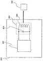
도 2의 판독기/기입기(201)는 도 5를 참조하여 기술되는 것이 주의된다. 도 5의 판독기/기입기(500)는 수신부(501), 전송부(502), 제어부(503), 인터페이스 부(504) 및 안테나 회로들(505)을 포함한다. 제어부(503)는 인터페이스부(504)를 통하여 보다 높은 레벨 장치(506)의 제어에 의해 데이터 처리 명령 및 데이터 처리 결과를 출력하기 위하여 수신부(501) 및 전송부(502)를 제어한다. 전송부(502)는 RFID(100)에 전송될 데이터 처리 명령을 변조하고 안테나 회로들(505)로부터 전자기파로서 이를 출력한다. 수신부(501)는 안테나 회로들(505)에 의해 수신된 신호를 복조하고, 제어부(503)에 데이터 처리 결과로서 이를 출력한다.It is noted that the reader /
이 실시예 모드에서, 도 5에 도시된 판독기/기입기(500)의 안테나 회로들(505)은 수신부(501) 및 전송부(502)에 접속되고 각각의 안테나 회로들(505)은 LC 병렬 공진 회로를 형성하는 공진 캐패시터(508) 및 안테나(507)를 포함한다. 안테나 회로들(505)은 데이터를 수신하는 시간에서 전기 신호로서 RFID(100)로부터 출력된 신호에 의해 안테나 회로들(505)에 유도된 기전력을 수신한다. 게다가, 데이터를 전송하는 시간에, 전류는 안테나 회로들(505)을 통하여 흐르고, 안테나 회로들(505)은 RFID(100)에 신호들을 전송한다.In this embodiment mode, the
도 2의 충전기(202)가 도 6을 참조하여 기술되는 것이 주의된다. 도 6의 충전기(600)는 전송 제어부(601) 및 안테나 회로(602)를 포함한다. 전송 제어부(601)는 RFID(100)에 전송되도록 충전하기 위한 전기 신호를 변조하고, 충전을 위한 신호는 안테나 회로(602)로부터 전송된다.It is noted that the
이 실시예 모드에서, 도 6에 도시된 충전기(600)의 안테나 회로(602)는 전송 제어부(601)에 접속되고, LC 병렬 공진 회로를 형성하는 공진 캐패시터(604) 및 안테나(603)를 포함한다. 안테나 회로(602)에서, 전류는 안테나 회로(602)를 통하여 흐르고, RFID(100)에 충전을 위한 신호는 데이터를 전송하는 시간에서 안테나(603)에 의해 전송된다.In this embodiment mode, the
도 1에서, 제 1 안테나 회로(101) 및 제 2 안테나 회로(102)는 신호 처리 회로(103)를 가진 동일한 기판상에 적층되거나, 외부 안테나들로서 제공될 수 있다는 것이 주의된다.In FIG. 1, it is noted that the
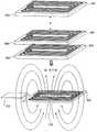
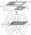
게다가, 이 실시예 모드에서, 제 1 안테나 회로(101) 및 제 2 안테나 회로(102)에 의해 수신된 신호들을 바람직하게 전자기 유도 방법에 의해 신호들의 통신을 수행한다. 따라서, 도 1 및 2의 RFID(100)는 바람직하게 제 1 코일 안테나 회로(101) 및 제 2 코일 안테나 회로(102)를 포함하는 구조를 가진다. 예를들어, 도 7은 제 1 안테나 회로 및 제 2 안테나 회로의 위치 관계, 및 RFID를 포함하는 반도체 장치의 안테나들 모양들을 도시한다. 도 7은 제 1 코일 안테나 회로(701) 및 제 2 코일 안테나 회로(702)가 각각 RFID(700)의 전면 표면 및 후면 표면상에 제공되고, 충전기의 안테나로부터의 신호가 수신되는 구조를 도시한다.In addition, in this embodiment mode, the signals received by the
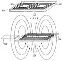
도 7에서, 전송 제어부(703)에 접속된 충전기의 안테나 회로(704)의 코일 안테나(705)가 RFID의 제 2 안테나 회로(702)에 밀접하게 될 때, AC 자기장은 충전기의 안테나 회로(704)의 코일 안테나(705)로부터 생성된다. AC 자기장은 RFID(700)의 제 2 코일 안테나 회로(702)를 통하여 통과하여, 기전력은 전자기 유도로 인해 RFID(700)의 제 2 코일 안테나 회로(702)의 단자들(안테나의 한쪽 단부와 다른쪽 단부 사이) 사이에 생성된다. RFID(700)의 배터리는 기전력에 의해 변화될 수 있다. 도 8에 도시된 바와 같이, RFID들(800)이 중첩될 때에도 RFID(800)의 기판의 전면 표면 또는 후면 표면상에 제공된 충전을 위한 제 2 안테나 회로(801)가 충전기로부터 충전될 수 있는 것이 주의된다. 도 9에 도시된 바외에, RFID(900)는 제 1 안테나 회로(901) 및 제 2 안테나 회로(902)가 동일한 기판상에서 나란히 배열될 수 있고, 충전기의 안테나 회로(704)로부터의 신호가 수신되는 구조를 가질 수 있다.In FIG. 7, when the
제 1 안테나 회로(101)와 판독기/기입기(201) 사이에서 전송 및 수신되는 신호의 주파수가 125 kHz, 13.56MHz, 915MHz, 2.45GHz, 또는 등등이고, 그 각각이 ISO 또는 등등에 의해 표준화되는 것이 주의된다. 자연스럽게, 안테나 회로(101)와 판독기/기입기(201) 사이에서 전송 및 수신되는 신호의 주파수가 이것으로 제한되지 않고, 예를들어 다음 중 임의의 것은 사용된다: 300GHz 내지 3THz의 서브밀리미터 파; 30GHz 내지 300GHz의 밀리미터파; 3GHz 내지 30GHz의 마이크로파; 300MHz 내지 3GHz의 초단파; 30MHz 내지 300MHz의 극 초단파; 3MHz 내지 30MHz의 단파; 300KHz 내지 3MHZ의 중간파; 30KHz 내지 300KHMz의 장파; 및 3KHz 내지 30KHz의 극장파. 게다가, 제 1 안테나 회로(101)와 판독기/기입기(201) 사이에서 전송되고 수신된 신호는 캐리어 파가 변조되는 신호이다. 캐리어 파의 변조 방법은 아날로그 변조 또는 디지털 변조일 수 있거나, 진폭 변조, 위상 변조, 주파수 변조, 및 확산 스펙트럼 중 임의의 것일 수 있다. 바람직하게, 진폭 변조 또는 주파수 변조는 사용될 수 있다.The frequency of the signal transmitted and received between the
제 2 안테나 회로(102)와 충전기(202) 사이에 전송되고 수신된 신호의 주파수가 m(m은 양수이다)으로 설정되고 제 1 안테나 회로(101) 및 판독기/기입기(201) 에 의해 전송 및 수신된 신호의 주파수가 M(M은 양수이다)으로 설정될 때, 0.5m<M<1.5m 및 m≠M의 관계를 만족하는 주파수는 바람직하게 사용된다. 제 2 안테나 회로(102)에 입력된 신호의 주파수가 상기 범위내에 설정될 때, 설계는 바람직한 제 1 안테나 회로(101) 및 제 2 안테나 회로(102)의 모양들을 크게 변화시키지 않고 수행될 수 있다.The frequency of the signal transmitted and received between the
전력이 두 가지 방식에 의해 도 1 및 2의 전원 회로(106)에 공급될 수 있다는 것은 주의된다: 하나의 방식은 캐리어 파의 신호가 통상적인 실시예에 기술된 패시브 타입 RFID와 유사하게 제 1 정류기 회로(105)에서 정류되도록 이루어진 전원 방식이고, 신호 처리 회로(103)의 각각의 회로를 구동하는 전원은 전원 회로(106)를 통하여 생성되고; 다른 방식은 배터리(104)가 제 2 정류기 회로(107)를 통하여 제 2 안테나 회로(102)로부터 입력된 배터리 충전 신호에 의해 충전되도록 이루어진 전원 방식이고, 배터리(104)에서 충전된 전력은 공급된다. 배터리(104)에서 충전된 전력은 통신 거리가 확장될 때 충분한 전력이 RFID(100)의 제 1 안테나 회로(101)로부터 얻어질 수 없는 경우 전원 회로(106)에 공급될 수 있다.It is noted that power can be supplied to the
도 1 및 2의 전원 회로의 예는 도 10을 참조하여 기술된다. 전원 회로는 기준 전압 회로 및 버퍼 증폭기를 포함한다. 기준 전압 회로는 레지스터(1001), 다이오드 접속 트랜지스터들(1002 및 1003)을 포함하고, 트랜지스터의 두 배의 VGS의 등가물인 기준 전압을 생성한다. 버퍼 증폭기는 트랜지스터들(1005 및 1006)을 포함하는 차동 회로; 트랜지스터들(1007 및 1008)을 포함하는 전력 미러 회로; 및 전류 공급 트랜지스터(1004), 트랜지스터(1009), 및 레지스터(1010)를 포함하는 공통 소스 증폭기를 포함한다.Examples of the power supply circuits of FIGS. 1 and 2 are described with reference to FIG. 10. The power supply circuit includes a reference voltage circuit and a buffer amplifier. The reference voltage circuit includes a
도 10에 도시된 전원 회로에서, 출력 단자로부터 흐르는 전류가 클 때, 트랜지스터(1009)에 공급되는 전류는 작고, 출력 단자로부터 흐르는 전류가 작을 때, 트랜지스터(1009)에 공급되는 전류는 크다. 따라서, 동작은 수행되어 레지스터(1010)로 흐르는 전류는 일정하다. 게다가, 출력 단자의 전위는 기준 전압 회로와 거의 동일한 값을 가진다. 여기서, 기준 전압 회로 및 버퍼 증폭기를 포함하는 전원 회로는 도시되고; 그러나, 본 발명은 도 10의 전원 회로로 제한되지 않고 다른 회로들일 수 있다.In the power supply circuit shown in Fig. 10, when the current flowing from the output terminal is large, the current supplied to the
이 명세서에서, 배터리는 충전에 의하여 계속 사용 시간에 복구할 수 있는 셀을 의미한다. 시트형 셀은 바람직하게 배터리로서 사용되는 것이 주의된다. 예를들어, 배터리는 리튬 셀, 바람직하게 젤 형 전해질을 사용하는 리튬 폴리머 셀, 리튬 이온 셀, 또는 등등을 사용하여 보다 작아질 수 있다. 자연스럽게, 임의의 셀은 셀이 충전할 수 있는 한 배터리로서 사용될 수 있고, 니켈 금속 하이브리드 셀 또는 니켈 카드듐 셀 같은 충전 및 방전 가능 셀은 사용될 수 있거나, 높은 캐패시티 또는 등등을 가진 캐패시터는 사용될 수 있다.In this specification, a battery means a cell that can be restored at a time of continuous use by charging. It is noted that the sheet cell is preferably used as a battery. For example, the battery can be smaller using lithium cells, preferably lithium polymer cells using a gel electrolyte, lithium ion cells, or the like. Naturally, any cell can be used as a battery as long as the cell can charge, and charge and dischargeable cells such as nickel metal hybrid cells or nickel cadmium cells can be used, or capacitors with high capacitance or the like can be used. have.
다음, 데이터가 판독기/기입기(201)로부터 도 1 및 2에 도시된 RFID(100)에 전송될 때의 동작은 하기에 기술된다. 제 1 안테나 회로(101)에 의해 수신된 신호는 제 1 정류기 회로(105)에 의해 반파 정류되고 평활화된다. 제 1 정류기 회로(105)에 의해 정류되고 평활화되는 전압은 전원 회로(106)에 입력된다. 전원 회로는 제 1 정류기 회로(105), 전원 회로(106), 제 2 정류기 회로(107), 복조 회 로(108), 증폭기(109), 논리 회로(110), 메모리 제어 회로(111), 메모리 회로(112), 논리 회로(113), 증폭기(114), 및 변조 회로(115)에 안정화된 전압을 공급한다.Next, the operation when data is transferred from the reader /
게다가, 제 1 안테나 회로(101)에 의해 수신된 신호는 증폭기(109)를 통하여 클럭 신호로서 논리 회로(110)에 입력된다. 게다가, 제 1 안테나 회로(101)로부터 입력된 신호는 복조 회로(108)에 의해 복조되고 데이터로서 논리 회로(110)에 입력된다.In addition, the signal received by the
논리 회로(110)에서, 입력된 데이터는 디코드된다. 판독기/기입기(201)는 변형 미러 코드, NRZ-L 코드, 또는 등등으로 인코드된 후 데이터를 전송하고 논리 회로(110)에 의해 디코드된다. 디코드된 데이터는 메모리 제어 회로(111)에 전송되고; 따라서, 메모리 회로(112)에 저장된 데이터는 판독된다. 메모리 회로(112)는 전력이 오프될 때에도 데이터를 저장할 수 있는 비휘발성 메모리 회로이고, 마스킹된 ROM 또는 등등은 사용된다.In
게다가, 판독기/기입기(201)가 도 1 및 2에 도시된 RFID(100)의 메모리 회로(112)에 저장된 데이터를 수신할 때, 동작은 다음과 같이 수행된다. 제 1 안테나 회로(101)에 의해 수신된 신호는 반파 정류되고 제 1 정류기 회로(105)에 의해 평활화된다. 반파 정류되고 제 1 정류기 회로(105)에 평활화된 전압은 전원 회로(106)에 입력된다. 전원 회로는 제 1 정류기 회로(105), 전원 회로(106), 제 2 정류기 회로(107), 복조 회로(108), 증폭기(109), 논리 회로(110), 메모리 제어 회로(111), 메모리 회로(112), 논리 회로(113), 증폭기(114), 및 변조 회로(115)에 안정된 전압을 공급한다.In addition, when the reader /
게다가, 제 1 안테나 회로(101)에 의해 수신된 AC 신호는 증폭기(109)를 통하여 논리 회로(110)에 입력되고, 논리 동작은 수행된다. 그 다음, 메모리 제어 회로(111)는 논리 회로(110)로부터 신호를 사용하여 제어되고, 메모리 회로(112)에 저장된 데이터는 호출된다. 메모리 회로(112)로부터 호출된 데이터는 논리 회로(113)에 의해 처리되고, 증폭기(114)에 의해 증폭되고, 그 다음 변조 회로(115)는 동작된다. 비록 데이터 처리가 ISO14443, ISO15693, 또는 ISO18000 같은 표준에 따라 수행되지만, 판독기/기입기와 호환성이 보장되는 한 이들 표준들과 다른 처리 시스템은 채택될 수 있다.In addition, the AC signal received by the
변조 회로(115)가 동작할 때, 제 1 안테나 회로(101)는 변화된다. 따라서, 제 1 안테나 회로(101)에서 반사된 판독기/기입기(201)의 신호는 변화한다. 판독기/기입기가 이런 변화를 판독할 때, RFID(100)의 메모리 회로(112)에 저장된 데이터는 인식될 수 있다. 상기 변조 방법은 로드 변조 방법이라 한다.When the
다음, 전력이 충전기(202)에 의해 도 1 및 2에 도시된 RFID(100)에서 충전될 때의 동작은 하기에 기술된다. 제 2 안테나 회로에 의해 수신된 신호는 제 2 정류기 회로(107)에 의해 반파 정류되고 평활화된다. 제 정류기 회로(107)에 반파 정류되고 평활화된 전압은 일단 배터리(104)에 유지된다. 배터리(104)에 유지된 전력은 전원 회로(106)에 공급될 전력으로서 사용된다. 제 1 안테나 회로에 의해 공급된 신호가 수신되지만 판독기/기입기에 신호를 전송하기 위한 전력 부족이 있을 때, 전력이 배터리에 의해 공급되는지를 결정하는 회로가 구비된 구조는 사용될 수 있다.Next, the operation when the power is charged in the
다음, 도 1에 도시된 RFID(100)의 평면도의 예는 도시된다. RFID(100)의 기능 및 크기 측면에서, RFID(100)는 제 1 안테나 회로, 제 2 안테나 회로, 신호 처리 회로, 및 배터리가 기판상에 나란히 적층되거나 배열되는 레이아웃을 가질 수 있다. 게다가, 신호 처리 회로는 제 1 안테나 회로와 연관된 회로 및 제 2 안테나 회로와 연관된 회로로 분할될 수 있다. 제 1 안테나 회로와 연관된 회로는 제 1 신호 처리 회로라 하고, 제 2 안테나 회로와 연관된 회로는 제 2 신호 처리 회로라 한다. 특히, 제 1 신호 처리 회로는 도 1의 제 2 정류기 회로(107)에 해당하고, 제 2 신호 처리 회로는 도 1의 신호 처리 회로(103)의 제 2 정류기 회로와 다른 구조에 해당한다. 도 11a 및 11b에 도시된 평면도들은 제 1 안테나 회로(1101), 제 2 안테나 회로(1102), 제 1 신호 처리 회로(1130A), 제 2 신호 처리 회로(1103B), 및 배터리(1104) 사이의 위치 관계들의 예들을 도시한다.Next, an example of the top view of the
예를들어 도 11a에 도시된 평면도의 구조는 제 1 안테나 회로(1101), 제 2 안테나 회로(1102), 제 1 신호 처리 회로(1103A), 및 제 2 신호 처리 회로(1103B)가 하나의 표면상에 제공되고; 및 배터리(1104)가 다른 표면상에 제공되는 구조일 수 있다. 게다가, 도 11b에 도시된 평면도의 구조는 제 1 안테나 회로(1101) 및 제 1 신호 처리 회로(1103A)가 하나의 표면상에 제공되고; 제 2 안테나 회로(1102) 및 제 2 신호 처리 회로(1103B)가 다른 표면상에 제공되고; 및 배터리(1104)가 제 1 신호 처리 회로(1103A)와 제 2 신호 처리 회로(1103B) 사이에 제공되는 구조일 수 있다.For example, the structure of the plan view shown in FIG. 11A is such that the
도 11a 및 도 11b에서, RFID의 배터리(1104)의 위치가 배터리(1104)를 도시함으로써 기술되고; 그러나, 본 발명이 배터리들의 종류들에 따라 이것으로 제한되지 않는다는 것이 주의된다. 예를들어, 약 10㎛ 내지 100㎛의 두께를 가지도록 얇은 리튬 이온 제 2 셀은 제 1 신호 처리 회로(1103A) 또는 제 2 신호 처리 회로(1130B)와 동시에 형성될 수 있다. 게다가, 박막 캐패시터는 배터리(1104)로서 사용될 제 1 신호 처리 회로(1103A) 또는 제 2 신호 처리 회로(1103B)와 동시에 형성될 수 있다. 보다 작고 얇게 만들어진 배터리(1104), 제 1 신호 처리 회로(1103A), 및 제 2 신호 처리 회로(1103B)를 가진 RFID를 포함하는 반도체 장치는 바람직하게 넓은 융통성 및 넓은 애플리케이션 범위로 인해 사용될 수 있다.11A and 11B, the location of the
상기된 바와 같이, 본 발명의 RFID를 포함하는 반도체 장치는 배터리를 포함한다. 그러므로, 종래 반도체 장치와 유사하게, 본 발명의 반도체 장치는 셀의 시간에 따른 품질 저하와 연관된 개별 정보를 전송 및 수신하기 위한 전력 부족을 방지할 수 있다. 게다가, 본 발명의 반도체 장치는 배터리에 전력을 공급하기 위한 신호를 수신하는 안테나를 가진다. 그러므로, 외측으로부터 무선파들의 전력이 사용될 때, 배터리는 반도체 장치와 충전기 사이의 직접적인 접속없이 충전될 수 있다. 따라서, 본 발명의 반도체 장치는 액티브 타입 RFID 같은 셀의 나머지 캐패시티 및 셀의 교체를 확인하지 않고 계속 사용될 수 있다. 게다가, 전력은 배터리로 유지되어, RFID를 동작시키기 위한 충분한 전력은 얻어지고 판독기/기입기와 RFID 사이의 통신 거리는 확장될 수 있다.As described above, the semiconductor device including the RFID of the present invention includes a battery. Therefore, similar to the conventional semiconductor device, the semiconductor device of the present invention can prevent the power shortage for transmitting and receiving individual information associated with the deterioration of quality over time of the cell. In addition, the semiconductor device of the present invention has an antenna for receiving a signal for powering a battery. Therefore, when the power of radio waves from the outside is used, the battery can be charged without a direct connection between the semiconductor device and the charger. Therefore, the semiconductor device of the present invention can be used continuously without confirming the remaining capacity of the cell and the replacement of the cell, such as an active type RFID. In addition, power is maintained by the battery so that sufficient power for operating the RFID can be obtained and the communication distance between the reader / writer and the RFID can be extended.
이 실시예 모드가 이 명세서의 다른 실시예의 설명과 결합하여 실행될 수 있 는 것은 주의된다.It is noted that this embodiment mode may be practiced in conjunction with the descriptions of other embodiments in this specification.
(실시예 모드 2)(Embodiment Mode 2)
이 실시예 모드는 도면들을 참조하여 실시예 모드 1에 도시된 RFID를 가진 반도체 장치에서 부스트 안테나 회로(이후 부스터 안테나라 함)를 가진 구조를 기술할 것이다. 이 실시예 모드에서 사용되는 도면들에서, 동일한 참조 번호들은 실시예 모드 1과 동일한 부분들에 사용되는 것이 주의된다.This embodiment mode will describe a structure having a boost antenna circuit (hereinafter referred to as booster antenna) in the semiconductor device with RFID shown in
이 실시예 모드에 기술된 부스터 안테나가 판독기/기입기로부터 신호를 수신하고 반도체 장치에 포함된 RFID의 신호 처리 회로에 이를 출력하는 안테나(이후, 제 1 칩 안테나 또는 제 1 안테나 회로라 함), 또는 반도체 장치에 포함된 충전기로부터 신호를 수신하는 안테나(이후 제 2 칩 안테나 또는 제 2 안테나 회로라 함)보다 큰 안테나(이후 부스터 안테나라 함)를 의미하는 것은 주의된다. 부스터 안테나 및 제 1 칩 안테나 또는 제 2 칩 안테나는 하나의 주파수 대역에서 공진하고 자기 결합되어, 판독기/기입기 또는 충전기에 의해 발진된 신호는 타켓 RFID로 효과적으로 전송될 수 있다. 부스터 안테나가 자기장을 통하여 코일 안테나에 접속되기 때문에, 부스터 안테나는 바람직한 칩 안테나 및 신호 처리 회로에 직접 접속되는 것이 요구되지 않는다.An antenna (hereinafter referred to as a first chip antenna or a first antenna circuit) in which the booster antenna described in this embodiment mode receives a signal from a reader / writer and outputs it to a signal processing circuit of RFID included in the semiconductor device, Or an antenna (hereinafter referred to as a booster antenna) that is larger than an antenna (hereinafter referred to as a second chip antenna or a second antenna circuit) that receives a signal from a charger included in the semiconductor device. The booster antenna and the first chip antenna or the second chip antenna are resonant and magnetically coupled in one frequency band so that the signal oscillated by the reader / writer or charger can be effectively transmitted to the target RFID. Since the booster antenna is connected to the coil antenna via a magnetic field, the booster antenna is not required to be directly connected to the desired chip antenna and signal processing circuit.
이 실시예 모드에서 RFID에 사용되는 반도체 장치는 도 12 및 13에 도시된 블록도를 참조하여 기술된다.Semiconductor devices used for RFID in this embodiment mode are described with reference to the block diagrams shown in Figs.
도 12의 RFID(100)는 제 1 안테나 회로(101), 제 2 안테나 회로(102), 부스터 안테나(1201), 신호 처리 회로(103), 및 배터리(104)를 포함한다. 신호 처리 회로(103)는 제 1 정류기 회로(105), 전원 회로(106), 제 2 정류기 회로(107), 복조 회로(108), 증폭기(109), 논리 회로(110), 메모리 제어 회로(111), 메모리 회로(112), 논리 회로(113), 증폭기(114), 및 변조 회로(115)를 포함한다.The
도 13은 부스터 안테나(1201)가 판독기/기입기(201)에 및 판독기/기입기로부터 신호를 전송 및 수신하고, 제 1 안테나 회로(101)에 자기 결합되어, 판독기/기입기로부터의 신호가 전송 및 수신되고, 제 2 안테나 회로(102)가 충전기(202)로부터 신호를 수신하는 블록도를 도시한다. 도 13에서, 부스터 안테나(1201)는 판독기/기입기(201)로부터 신호를 수신하고 전자기 유도에 따라 제 1 안테나 회로에 자기장 결합되어, 제 1 안테나 회로(101)에 의해 수신된 신호는 제 1 정류기 회로(105)를 통하여 전원 회로(106)에 입력되고 복조 회로(108) 및 증폭기(109)에 입력된다. 도 13에서 이외에, 제 2 안테나 회로(102)에 의해 수신된 신호는 제 2 정류기 회로(107)를 통하여 배터리(104)에 입력되고, 전력은 적당할 때 배터리(104)로부터 전원 회로(106)에 공급된다. 도 13에 도시된 구조에서, 판독기/기입기(201)와 RFID(100) 사이에서 신호의 전송 및 수신의 통신 거리는 실시예 모드 1보다 확장될 수 없고, 이것은 데이터가 보다 확실하게 전송 및 수신될 수 있기 때문에 바람직하다.13 shows that the
게다가, 부스터 안테나(1201)의 동조는 제 1 안테나 회로로 제한되지 않고, 부스터 안테나(1201)는 부스터 안테나(1201)가 동조되는 주파수 대역을 변화시킴으로써 다른 안테나에 자기 결합될 수 있다.In addition, tuning of the
예를들어, 도 14는 부스터 안테나(1201)가 충전기(202)로부터 신호를 수신하 고 제 2 안테나 회로(102)에 자기 결합되어, 충전기로부터의 신호가 수신되고 제 1 안테나 회로(101)가 판독기/기입기(201)에 및 상기 판독기/기입기로부터 신호를 전송 및 수신하는 블록도를 도시한다. 도 14에서, 부스터 안테나(1201)는 충전기(202)로부터 신호를 수신하고 전자기 유도에 따라 제 2 안테나 회로에 자기 결합되어, 제 2 안테나 회로(102)에 의해 수신된 신호는 제 2 정류기 회로(107)를 통하여 배터리(104)에 입력된다. 그 다음, 전력은 적당할 때 배터리(104)로부터 전원 회로(106)에 공급된다. 게다가 도 14에서, 제 1 안테나 회로(101)에 의해 수신된 신호는 제 1 정류기 회로(105)를 통하여 전원 회로(106)에 입력되고, 복조 회로(108) 및 증폭기(109)에 입력된다. 도 14에 도시된 구조에서, 충전기(202)와 RFID(100) 사이의 신호의 전송 및 수신의 통신 거리는 확장될 수 있고, 이것은 충전이 보다 확실하게 배터리로 수행될 수 있기 때문에 바람직하다.For example, FIG. 14 shows that the
게다가, 부스터 안테나(1201)의 동조는 제 1 안테나 회로 또는 제 2 안테나 어느 하나로 제한되지 않고, 부스터 안테나(1201)는 부스터 안테나(1201)가 동조되는 주파수 대역을 확장시킴으로써 다수의 안테나들에 자기 결합될 수 있다.In addition, tuning of the
예를들어, 도 15는 부스터 안테나(1201)가 판독기/기입기(201) 및 충전기(202)에 및 상기 판독기/기입기와 상기 충전기로부터 신호를 전송 및 수신하고 제 1 안테나 회로(101) 및 제 2 안테나 회로(102)에 자기 결합되어, 판독기/기입기로부터의 신호 및 충전기로부터의 신호가 전송 및 수신되는 블록도를 도시한다. 도 15에서, 부스터 안테나(1201)는 판독기/기입기(201)로부터 신호를 수신하고 전자기 유도에 따라 제 1 안테나 회로에 자기 결합되어, 제 1 안테나 회로(101)에 의 해 수신된 신호는 제 1 정류기(105)를 통하여 전원 회로(106)에 입력된다. 게다가, 도 15에서, 부스터 안테나(1201)는 충전기(202)로부터 신호를 수신하고 전자기 유도에 따라 제 2 안테나 회로에 자기 결합되어, 제 2 안테나 회로(102)에 의해 수신된 신호는 제 2 정류기 회로(107)를 통하여 배터리(104)에 입력된다. 따라서, 전력은 적당할 때 배터리(104)로부터 전원 회로(106)에 공급된다. 제 1 안테나 회로 및 제 2 안테나 회로가 동조되는 주파수들이 서로 근접하여, 부스터 안테나의 전자기 유도 효율성이 바람직하게 증가된다. 그러므로, 제 2 안테나 회로(102)와 충전기(202) 사이에서 전송 및 수신되는 신호의 주파수가 m(m은 양수이다)으로 설정되고 제 1 안테나 회로(101)와 판독기/기입기(201) 사이에서 전송 및 수신된 신호의 주파수가 M(M은 양수이다)로 설정될 때, 0.5m<M<1.5m의 관계 및 m≠M을 만족시키는 주파수는 바람직하게 사용된다. 상기 바람직한 효과외에, 제 2 안테나 회로(102)에 입력된 신호의 주파수가 상기 범위내에서 설정될 때, 설계는 제 1 안테나 회로(101) 및 제 2 안테나 회로(102)의 모양들을 크게 변화시키지 않고 수행될 수 있고, 이것은 바람직하다. 도 15에 도시된 구조에서, 판독기/기입기(201)와 RFID(100) 사이의 신호의 전송 및 수신, 그리고 충전기(202)와 RFID(100) 사이의 신호의 전송 및 수신의 통신 거리는 확장될 수 있고, 이것은 데이터가 보다 확실하게 전송 및 수신될 수 있고 충전이 보다 확실하게 배터리(104)로 수행될 수 있기 때문에 바람직하다.For example, FIG. 15 shows that the
제 1 안테나 회로(101), 제 2 안테나 회로(102), 및 부스터 안테나의 안테나 모양들이 특정하게 제한되지 않은 것이 주의된다. 예를들어, 실시예 모드 1에 기 술된 도 3b에 도시된 모양을 가진 안테나는 채택될 수 있다. 비자기 결합된 안테나 회로보다 큰 모양을 가진 안테나는 그 기능으로 인해 부스터 안테나로서 바람직하게 사용되는 것이 주의된다. 게다가, 제 1 안테나 회로(101), 제 2 안테나 회로(102), 및 부스터 안테나 각각은 실시예 모드 1에 기술된 도 4a에 도시된 바와 같이 안테나(401) 및 공진 캐패시터(402)를 포함하는 구조를 가지도록 기술되고, 안테나 회로(403)는 안테나(401) 및 공진 캐패시터(402)의 결합물을 말한다.It is noted that the antenna shapes of the
게다가, 도 12 내지 15에서 제 1 정류기 회로(105) 및 제 2 정류기 회로(107)는 실시예 모드 1에 도시된 것과 유사하고, 정류기 회로(407)는 도 4b에 도시된 바와 같이 다이오드(404), 다이오드(405), 및 평활화 캐패시터(406)를 포함한다.In addition, the
도 13 내지 15의 판독기/기입기(201)가 실시예 모드 1에 도시된 것과 유사하고, 도 5에 도시된 구조가 사용될 수 있다는 것은 주의된다.It is noted that the reader /
도 13 내지 15의 충전기(202)가 실시예 모드 1에 도시된 것과 유사하고, 도 6에 도시된 구조가 사용될 수 있다는 것은 주의된다.It is noted that the
도 13 내지 15에서, 제 1 안테나 회로(101) 및 제 2 안테나 회로(102)가 신호 처리 회로(103)를 가진 동일한 기판상에 적층되거나, 외부 안테나들로서 제공될 수 있다는 것은 주의된다.13-15, it is noted that the
이 실시예 모드에서, 제 1 안테나 회로(101), 제 2 안테나 회로(102), 및 부스터 안테나(1201)에 의해 수신된 신호들은 바람직하게 전자기 유도 방법에 의해 통신된다. 그러므로, 도 13 내지 15의 RFID(100)는 바람직하게 제 1 코일 안테나 회로(101), 제 2 코일 안테나 회로(102), 및 코일 부스터 안테나(1201)를 포함하는 구조를 가진다. 예를들어, 도 16은 제 1 안테나 회로, 제 2 안테나회로, 및 부스터 안테나 사이의 위치 관계, 및 도 14에 도시된 구조를 가진 RFID를 포함하는 반도체 장치의 안테나들의 모양들을 도시한다. 도 16은 제 1 코일 안테나 회로(1601) 및 제 2 코일 안테나 회로(1602)가 RFID(1600)의 표면상에 제공되고, 부스터 안테나(1603)가 RFID(1600)의 다른 표면상에 제공되고, 충전기의 안테나로부터의 신호가 수신되는 구조를 도시한다.In this embodiment mode, the signals received by the
도 16에서, 전송 제어부(1604)에 접속된 충전기의 안테나 회로(1605)의 코일 안테나(1606)가 RFID의 부스터 안테나(1603)에 근접할 때, AC 자기장은 충전기의 안테나 회로(1605)의 코일 안테나(1606)로부터 생성된다. AC 자기장은 RFID(1600)의 코일 부스터 안테나(1603)를 통하여 통과하고, 이에 따라 기전력은 전자기 유도로 인해 RFID(1600)의 코일 부스터 안테나(1603)의 단자들(안테나의 한쪽 단부와 다른쪽 단부 사이) 사이에 생성된다. 전자기 유도로 인한 기전력은 코일 부스터 안테나(1603)에서 생성되고, AC 자기장은 부스터 코일 자체로부터 생성된다. 그 다음, 부스터 안테나(1603)로부터 생성된 AC 자기장은 RFID(1600)의 제 2 코일 안테나 회로(1602)를 통하여 통과하여, 기전력은 전자기 유도로 인하여 RFID(1600)의 제 2 코일 안테나 회로(1602)의 단자들(안테나의 한쪽 단부와 다른쪽 단부 사이) 사이에 생성된다. RFID(1600)의 배터리는 기전력에 의해 충전될 수 있다.In Fig. 16, when the
게다가, 도 17은 도 16에 도시된 구조와 다른 구조를 도시한다. 도 17은 코일 부스터 안테나(1603)와 제 1 안테나 회로(1601) 또는 제 2 안테나 회로(1602)가 RFID(1600)의 하나의 표면상에 제공되고, 제 1 안테나 회로(1601) 및 제 2 안테나 회로(1602)의 다른 하나는 RFID(1600)의 다른 표면상에 제공되고, 여기서 충전기의 안테나로부터의 신호가 수신되는 구조를 도시한다. 도 17에서, 전송 제어부(1604)에 접속된 충전기의 안테나 회로(1605)의 코일 안테나(1606)가 RFID의 부스터 안테나(1603)에 밀접하게 될 때, AC 자기장은 충전기의 안테나 회로(1605)의 코일 안테나(1606)로부터 생성된다. AC 자기장이 RFID(1600)의 코일 부스터 안테나(1603)를 통하여 통과함으로써, 기전력은 전자기 유도로 인해 RFID(1600)의 코일 부스터 안테나(1603)의 단자들(안테나의 하나의 단부와 다른 단부 사이) 사이에 생성된다. 전자기 유도로 인한 기전력은 코일 부스터 안테나(1603)에 생성되고, AC 자기장은 부스터 코일 자체로부터 생성된다. 그 다음, 부스터 안테나(1603)로부터 생성된 AC 자기장은 RFID(1600)의 제 2 코일 안테나 회로(1602)를 통하여 통과하고, 기전력은 전자기 유도로 인해 RFID(1600)의 제 2 코일 안테나 코일(1602)의 단자들(안테나의 하나의 단부와 다른 단부 사이) 사이에 생성된다. RFID(1600)의 배터리는 기전력에 의해 충전될 수 있다. 이 실시예에서 제 1 안테나 회로, 제 2 안테나 회로, 및 부스터 안테나의 배열은 안테나들이 안테나 코일을 통하여 AC 자기장이 통과되도록 배치되게 설계될 수 있다. 게다가, 도 17에 도시된 바와 같이, 큰 영역을 유지하는 부스터 안테나 내에 제 1 안테나 회로 또는 제 2 안테나 회로를 배열함으로써, 효과적인 배열은 수행될 수 있고; 그러므로, 배터리 영역 또는 등등은 증가될 수 있고 안테나 권선들의 수는 바람직하게 증가될 수 있다.In addition, FIG. 17 shows a structure different from that shown in FIG. 17 illustrates that a
도 16 및 17에 도시된 RFID(1600)는 RFID들이 실시예 모드 1에서 도 8에 도 시된 바와 같이 중첩될 때에도 충전기로부터 충전될 수 있다.The
제 1 안테나 회로(101)와 판독기/기입기(201) 사이에서 전송되고 수신된 신호의 주파수는 실시예 모드 1과 유사하고, 그러므로, 설명들은 이 실시예 모드에서 생략되는 것이 주의된다.It is noted that the frequency of the signal transmitted and received between the
제 2 안테나 회로(102)와 충전기(202) 사이에서 전송 및 수신된 신호의 주파수가 실시예 모드 1과 유사하고; 그러므로, 설명은 이 실시예 모드에서 생략되는 것이 주의된다.The frequency of the signal transmitted and received between the
전력은 두 가지 방식으로 도 12 내지 15에서 전원 회로(106)에 공급될 수 있다는 것이 주의된다: 하나의 방식은 캐리어 파의 신호가 통상적인 실시예에 기술된 패시브 타입 RFID와 유사하게 제 1 정류기 회로(105)에서 정류되도록 이루어진 전원 방식이고, 신호 처리 회로(103)의 각각의 회로를 구동하는 전원은 전원 회로(106)를 통하여 생성되고; 다른 방식은 배터리(104)가 제 2 정류기 회로(107)를 통하여 제 2 안테나 회로(102)로부터 입력되는 배터리 충전 신호에 의해 충전되도록 이루어지는 전원 방식으로, 배터리(104)에서 충전된 전력은 공급된다. 배터리(104)에서 충전된 전력은 통신 거리가 확장할 때 RFID(100)의 제 1 안테나 회로(101)로부터 충분한 전력이 얻어질 수 없는 경우 전원 회로(106)에 공급될 수 있다.It is noted that power can be supplied to the
도 12 내지 15의 전원 회로(106)는 실시예 모드 1에서 도 10에 도시된 실시예와 유사하다; 그러므로, 설명은 이 실시예 모드에서 생략된다.The
게다가, 도 12 내지 15에 도시된 RFID의 동작은 실시예 모드 1에 기술된 동 작과 유사하고; 그러므로, 설명은 이 실시예 모드에서 생략된다.In addition, the operation of the RFID shown in Figs. 12 to 15 is similar to the operation described in
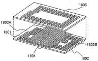
다음, 도 12에 도시된 RFID(100)의 평면도의 예는 도시된다. 도 12에 도시된 RFID(100)의 기능 및 크기 측면에서, RFID(100)는 제 1 안테나 회로, 제 2 안테나 회로, 부스터 안테나, 신호 처리 회로, 및 배터리가 기판상에 나란히 적층 또는 배열되는 레이아웃을 가질 수 있다. 게다가, 신호 처리 회로는 제 1 안테나 회로와 연관된 회로 및 제 2 안테나 안테나와 연관된 회로로 분할될 수 있다. 제 1 안테나 회로와 연관된 회로는 제 1 신호 처리 회로라 하고, 제 2 안테나 회로와 연관된 제 2 안테나 회로는 제 2 신호 처리 회로라 한다. 특히, 제 1 신호 처리 회로는 도 12의 제 2 정류기 회로(107)에 대응하고, 제 2 신호 처리 회로는 도 12의 신호 처리 회로(103)에서 제 2 정류기 회로와 다른 구조에 대응한다. 도 18에 도시된 평면도들은 제 1 안테나 회로(1801), 제 2 안테나 회로(1802), 제 1 신호 처리 회로(1803A), 제 2 신호 처리 회로(1803B), 배터리(1804), 및 부스터 안테나(1805) 사이의 위치 관계의 예를 도시한다.Next, an example of the top view of the
예로서 도 18에 도시된 평면도 구조는 제 1 안테나 회로(1801), 제 2 안테나 회로(1802), 제 1 신호 처리 회로(1803A), 및 제 2 신호 처리 회로(1803B)가 하나의 표면상에 제공되고; 부스터 안테나(1805)가 다른 표면상에 제공되고; 및 배터리(1804)가 제 1 신호 처리 회로(1803A)와 제 2 신호 처리 회로(1803B) 사이에 제공되는 구조일 수 있다.As an example, the plan view structure shown in FIG. 18 shows that the
도 18에서, RFID의 배터리(1804)의 위치는 배터리(1804)를 도시함으로써 기술되고; 그러나, 본 발명은 배터리들의 종류에 따라 이것으로 제한되지 않는다. 예를들어, 약 10㎛ 및 100㎛의 두께를 가지도록 얇은 리튬 이온 제 2 셀은 제 1 신호 처리 회로(1803A) 또는 제 2 신호 처리 회로(1803B)와 동시에 형성될 수 있다. 게다가, 박막 캐패시터는 배터리(1804)로서 사용될 제 1 신호 처리 회로(1803A) 또는 제 2 신호 처리 회로(1803B)와 동시에 형성될 수 있다. 얇은 배터리(1804)를 가진 RFID 및 작고 얇은 제 1 신호 처리 회로(1803A) 또는 제 2 신호 처리 회로(1803B)를 포함하는 반도체 장치는 바람직하게 넓은 융통성, 넓은 애플리케이션 범위, 및 짧아진 제조 처리로 인해 사용될 수 있다.In FIG. 18, the location of the
상기된 바와 같이, 본 발명의 RFID를 포함하는 반도체 장치는 배터리를 포함한다. 그러므로, 종래 반도체 장치와 유사하게, 본 발명의 반도체 장치는 셀의 시간에 따른 품질 저하와 연관된 개별 정보를 전송 및 수신하기 위한 전력 부족을 방지할 수 있다. 게다가, 본 발명의 반도체 장치는 배터리에 전력을 공급하기 위한 신호를 수신하는 안테나를 가진다. 그러므로, 외부로부터 무선 파들의 전력이 사용될 때, 배터리는 반도체 장치와 충전기 사이의 직접적인 접속 없이 충전될 수 있다. 따라서, 본 발명의 반도체 장치는 액티브 타입 RFID와 같이 셀의 나머지 캐패시티 및 셀의 교체의 확인 없이 계속하여 사용될 수 있다. 게다가, RFID를 구동하기 위한 전력은 배터리에서 항상 유지되어, RFID를 동작시키기에 충분한 전력은 얻어질 수 있고, 판독기/기입기와 RFID 사이의 통신 거리는 확장될 수 있다.As described above, the semiconductor device including the RFID of the present invention includes a battery. Therefore, similar to the conventional semiconductor device, the semiconductor device of the present invention can prevent the power shortage for transmitting and receiving individual information associated with the deterioration of quality over time of the cell. In addition, the semiconductor device of the present invention has an antenna for receiving a signal for powering a battery. Therefore, when the power of radio waves from the outside is used, the battery can be charged without a direct connection between the semiconductor device and the charger. Therefore, the semiconductor device of the present invention can be used continuously without confirmation of the remaining capacity of the cell and the replacement of the cell, like the active type RFID. In addition, the power for driving the RFID is always maintained in the battery, so that sufficient power to operate the RFID can be obtained, and the communication distance between the reader / writer and the RFID can be extended.
게다가, 이 실시예의 구조는 실시예 모드 1의 구조 외에 부스터 안테나를 가진다. 그러므로, RFID와 판독기/기입기 사이에서 데이터를 전송 및 수신하고 RFID에 의해 충전기로부터 충전을 위한 신호를 수신하기 위하여 통신이 확실하게 수행 될 수 있는 장점이 있다.In addition, the structure of this embodiment has a booster antenna in addition to the structure of
이 실시예 모드가 이런 명세서에서 다른 실시예 모드의 설명과 결합하여 실행될 수 있다는 것은 주의된다.It is noted that this embodiment mode may be practiced in conjunction with the description of other embodiment modes in this specification.
(실시예 모드 3)(Embodiment Mode 3)
이런 실시예 모드는 도면들을 참조하여 상기 실시예 모드들에 도시된 반도체 장치를 제조하기 위한 방법의 실시예를 기술할 것이다.This embodiment mode will describe an embodiment of a method for manufacturing the semiconductor device shown in the above embodiment modes with reference to the drawings.
첫째, 릴리스(release) 층(1903)은 그 사이에 배치된 절연 필름(1902)을 가진 기판(1901)의 하나의 표면상에 형성되고, 추후 베이스 필름 및 반도체 필름(1905)(예를들어 비결정질 실리콘 함유 필름)으로서 사용하는 절연 필름(1904)은 도 19a에서 적층된다. 절연 필름(1902), 릴리스 층(1903), 절연 필름(1904), 및 반도체 필름(1905)이 추후 형성되는 것은 주의된다.First, a
기판(1901)으로서, 유리 기판, 석영 기판, 금속 기판(세라믹 기판 또는 스테인레스 스틸 기판 같은), 또는 Si 기판 같은 반도체 기판이 사용될 수 있는 것은 주의된다. 게다가, 플라스틱 기판으로서, 폴리에틸렌 테레프탈레이트(PET), 폴리에틸렌 나프탈레이트(PEN), 폴리에테르 술폰(PES), 아크릴, 또는 등등으로 형성된 기판은 사용될 수 있다. 이런 과정에서, 릴리스 층(1903)은 그 사이에 배치된 절연 필름(1902)을 가진 기판(1901)의 전체 표면상에 제공된다. 그러나, 릴리스 층은 기판(1901)의 전체 표면상에 제공되고, 그 다음 릴리스 층은 만약 필요하다면 포토리소그래피 방법에 의해 선택적으로 제공될 수 있다.As the
절연 필름(1902) 및 절연 필름(1904)은 CVD 방법, 스퍼터링 방법, 또는 등등 에 의해 실리콘 옥사이드, 실리콘 니트라이드, 실리콘 옥시니트라이드(SiOxNy)(x>y>0), 또는 실리콘 니트라이드 옥사이드(SiNxOy)(x>y>0)로 형성된다. 예를들어, 절연 필름(1902) 및 절연 필름(1904)이 각각 두 개의 층 구조를 가지는 경우, 실리콘 니트라이드 옥사이드 필름은 제 1 절연 필름으로 형성되고 실리콘 옥시니트라이드 필름은 제 2 절연 필름으로서 형성될 수 있다. 선택적으로, 실리콘 니트라이드 필름은 제 1 절연 필름으로서 형성될 수 있고 제 2 옥사이드 필름은 제 2 절연 필름으로서 형성될 수 있다. 절연 필름(1902)은 불순물 엘리먼트가 기판(1901)으로부터 릴리스 층(1903) 또는 그 위에 형성된 엘리먼트에 혼합되는 것을 방지하는 차단 층으로서 기능한다. 절연 필름(1904)은 불순물 엘리먼트가 기판(1901) 및 릴리스 층(1903)으로부터 절연 필름(1904) 상에 형성된 엘리먼트로 혼합되는 것을 방지하는 차단 층으로서 기능한다. 이런 방식으로 블록킹 층으로서 각각 기능하는 절연 필름(1902) 및 절연 필름(1904)을 형성함으로써, 기판(1901)에서 Na 같은 알칼리 토류 금속 또는 알칼리 금속, 또는 릴리스 층(1903)에 포함된 불순물 엘리먼트가 절연 필름(1904) 상에 형성될 엘리먼트에 악영향을 미치는 것을 방지하는 것은 가능하다. 기판(1901)으로서 석영을 사용하는 경우, 절연 필름(1902) 및 절연 필름(1904)은 생략될 수 있다.The insulating
릴리스 층(1903)으로서, 금속 필름, 금속 필름의 적층된 층 구조 및 금속 옥사이드 필름, 또는 등등은 사용될 수 있다. 금속 필름은 텅스텐(W), 몰리브덴(Mo), 티타늄(Ti), 탄탈륨(Ta), 니오븀(Nb), 니켈(Ni), 코발트(Co), 지르코 늄(Zr), 아연(Zn), 루테늄(Ru), 로듐(Rh), 팔라듐(Pd), 오스뮴(Os) 또는 이리듐(Ir), 또는 메인 성분으로서 상기된 엘리먼트를 포함하는 합금 재료 또는 화합물 재료로부터 선택된 엘리먼트로 형성된 필름의 단일 층 또는 적층된 층들로서 형성된다. 금속 필름은 이들 재료들을 사용하여 스퍼터링 방법, 플라즈마 CVD 방법 같은 다양한 CVD 방법들, 또는 등등에 의해 형성될 수 있다. 상기된 금속 필름이 형성된 후 금속 필름 및 금속 옥사이드의 적층된 층 구조로서, 금속 필름의 옥사이드 또는 옥시니트라이드는 산소 분위기 또는 N2O 분위기에서 플라즈마 처리, 또는 산소 번위기 또는 N2O 분위기에서 열 처리를 수행함으로써 금속 필름 표면 상에 형성될 수 있다. 예를들어, 텅스텐 필름이 스퍼터링 방법, CVD 방법, 또는 등등에 의해 형성되는 경우, 금속 필름으로서, 텅스텐 옥사이드의 금속 옥사이드 필름은 텅스텐 필름상 플라즈마 처리를 수행함으로써 텅스텐 필름 표면상에 형성될 수 있다. 이 경우, 텅스텐의 옥사이드는 WOx로 표현되고 x는 2 내지 3이다. x=2(WO2), x=2.5(W2O5), x=2.75(W4O11), x=3(WO3), 및 등등의 경우들이 있다. 텅스텐의 옥사이드가 형성될 때, 상기된 x의 값은 특히 제한되지 않고, 어느 산화물이 형성되는가는 에칭 레이트 또는 등등을 바탕으로 결정될 수 있다. 선택적으로, 예를들어, 금속 필름(텅스텐 같은)은 형성될 수 있고, 실리콘 옥사이드(SiO2)의 절연 필름 또는 등등은 스퍼터링 방법에 의해 금속 필름 상에 형성될 수 있고, 금속 옥사이드는 금속 필름(예를들어, 텅스텐상에 텅스텐 옥사이드) 상에 형성될 수 있다. 게다가, 플라즈마 처리로서, 상기된 고밀도 플라즈마 처리는 예를들어 수행될 수 있다. 게다가, 금속 옥사이드 필름과 달리, 금속 니트라이드 또는 금속 옥시니트라이드는 또한 사용될 수 있다. 이 경우, 금속 필름은 질소 분위기 또는 질소 및 산소 분위기에서 플라즈마 처리 또는 열 처리될 수 있다.As the
반도체 필름(1905)은 스퍼터링 방법, LPCVD 방법, 플라즈마 CVD 방법, 또는 등등에 의해 25 내지 200nm(바람직하게 30 내지 150nm)의 두께로 형성된다.The
다음, 반도체 필름(1905)은 도 19b에 도시된 바와 같이 레이저 광으로 조사됨으로써 결정화된다. 반도체 필름(1905)은 레이저 조사 방법이 RTA 또는 어닐링 노를 사용한 열적 결정화 방법 또는 결정화를 촉진하기 위한 금속 엘리먼트를 사용하는 열적 결정화 방법과 결합될 수 있는 방법 또는 등등에 의해 결정화될 수 있다. 그 후, 얻어진 결정 반도체 필름은 목표된 모양을 가지도록 에칭된다; 이에 따라 결정 반도체 필름들(1905a 내지 1905f)을 형성한다. 그 다음, 게이트 절연 필름(1906)은 결정 반도체 필름들(1905a 내지 1905f)을 커버하기 위하여 형성된다.Next, the
게이트 절연 필름(1906)은 CVD 방법, 스퍼터링 방법, 또는 등등에 의해 실리콘 옥사이드, 실리콘 니트라이드, 실리콘 옥시니트라이드(SiOxNy)(x>y>0), 또는 실리콘 니트라이드 옥사이드(SiNxOy)(x>y>0) 같은 절연 재료로 형성된다. 예를들어, 게이트 절연 필름(1906)이 두 개의 층 구조를 가지는 경우, 실리콘 옥시니트라이드 필름은 제 1 절연 필름으로서 형성되고 실리콘 니트라이드 옥사이드 필름은 제 2 절연 필름으로서 형성될 수 있다. 선택적으로, 실리콘 옥사이드 필름은 제 1 절연 필름으로서 형성될 수 있고 실리콘 니트라이드 필름은 제 2 절연 필름으로서 형성될 수 있다.
결정질 반도체 필름들(1905a 내지 1905f)의 제조 단계의 예는 이하에 짧게 기술될 것이다. 첫째, 50 내지 60nm의 두께를 가진 비결정질 반도체 필름은 플라즈마 CVD 방법에 의해 형성된다. 다음, 결정화를 촉진하기 위한 금속 엘리먼트인 니켈 함유 용액은 비결정질 반도체 필름 상에 보유되고, 탈수소반응 처리(한 시간 동안 500℃에서) 및 열적 결정화 처리(4시간 동안 550℃에서)는 비결정질 반도체 필름상에서 수행되어; 결정질 반도체 필름을 형성한다. 그 후, 결정질 반도체 필름은 레이저 광이 조사되고, 포토리소그래피 방법은 사용되어, 결정질 반도체 필름들(1905a 내지 1905f)은 형성된다. 결정화를 촉진하기 위한 금속 엘리먼트를 사용하는 열적 결정화를 수행하지 않고, 비결정질 반도체 필름은 레이저 광 조사에 의해서만 결정화될 수 있다는 것이 주의된다.Examples of the manufacturing steps of the
결정화에 사용된 레이저 발진기로서, 연속 파 레이저 빔(CW 레이저 빔) 또는 펄스파 레이저 빔(펄스 레이저 빔)은 사용될 수 있다. 여기에 사용될 수 있는 레이저 빔으로서, 하나 또는 그 이상의 다음에서 방출되는 레이저 빔은 사용될 수 있다: Ar 레이저, Kr 레이저 또는 익사이머 레이저 같은 가스 레이저; 도판트로서 하나 또는 그 이상의 Nd, Yb, Cr, Ti, Ho, Er, Tm 및 Ta가 부가되는 매체가 단일 결정 YAG, YVO4, 고토감란석(Mg2SiO4), YAlO3, GdVo4, 또는 다결정질(세라믹) YAG, Y2O3, YVO4, YAlO3, GdVO4인 레이저; 유리 레이저; 루비 레이저; 알렉사트라이트 레 이저; Ti:사파이어 레이저; 구리 기상 레이저; 또는 금 기상 레이저. 상기 레이저 빔들의 기본 파들 또는 상기 기본파들의 제 2 내지 제 4 고조파들이 사용될 때 큰 그레인 크기를 가진 결정들을 얻는 것은 가능하다. 예를들어, Nd:YVO4 레이저(1064nm의 기본파)의 제 2 고조파(532nm) 또는 제 3 고조파(355nm)는 사용될 수 있다. 이 때 레이저의 에너지 밀도는 약 0.01 내지 100MW/cm2(바람직하게, 0.1 내지 10 MW/cm2)이도록 요구된다. 조사는 약 10 내지 2000 cm/sec의 스캐닝 속도로 수행된다. 도판트로서 하나 또는 그 이상의 Nd, Yb, Cr, Ti, Ho, Er, Tm 및 Ta가 부가된 매체로서 단일 결정 YAG, YVO4, 고토감람석(Mg2SiO4), YAlO3, 또는 GdVO4 또는 다결정(세라믹) YAG, Y2O3, YVO4, YAlO3, 또는 GdVO4를 사용하는 레이저; Ar 이온 레이저; 또는 Ti 사파이어 레이저는 계속 발진될 수 있다. 게다가, 이들의 펄스 발진은 Q 스위치 동작, 모드 동기화 또는 등등을 수행함으로써 10 MHz 또는 그 이상의 반복 속도로 수행될 수 있다. 레이저 빔이 10MHz 또는 그 이상의 반복율로 발진되는 경우, 반도체 필름이 레이저에 의해 용융된 후 및 고형화되기 전에, 반도체 필름은 다음 펄스로 조사된다. 그러므로, 낮은 반복율을 가진 펄스 레이저를 사용하는 경우와 달리, 고체-액체 인터페이스는 반도체 필름에서 계속하여 이동될 수 있고, 이에 따라 스캐닝 방향으로 계속 성장하는 결정 그레인들은 얻어질 수 있다.As the laser oscillator used for crystallization, a continuous wave laser beam (CW laser beam) or a pulse wave laser beam (pulse laser beam) can be used. As a laser beam that can be used here, one or more laser beams emitted may be used: gas lasers such as Ar lasers, Kr lasers or excimer lasers; As the dopant, the medium to which one or more of Nd, Yb, Cr, Ti, Ho, Er, Tm and Ta is added is selected from single crystals YAG, YVO4 , Gotoranite (Mg2 SiO4 ), YAlO3 , GdVo4 , Or a laser which is polycrystalline (ceramic) YAG, Y2 O3 , YVO4 , YAlO3 , GdVO4 ; Glass laser; Ruby laser; Alexalite laser; Ti: sapphire laser; Copper vapor laser; Or gold vapor laser. It is possible to obtain crystals with large grain size when the fundamental waves of the laser beams or the second to fourth harmonics of the fundamental waves are used. For example, a second harmonic (532 nm) or third harmonic (355 nm) of an Nd: YVO4 laser (fundamental wave of 1064 nm) may be used. The energy density of the laser is then required to be about 0.01 to 100 MW / cm2 (preferably 0.1 to 10 MW / cm2 ). Irradiation is performed at a scanning speed of about 10-2000 cm / sec. Single crystals YAG, YVO4 , Gobletolite (Mg2 SiO4 ), YAlO3 , or GdVO4 , as media doped with one or more of Nd, Yb, Cr, Ti, Ho, Er, Tm and Ta Laser using polycrystalline (ceramic) YAG, Y2 O3 , YVO4 , YAlO3 , or GdVO4 ; Ar ion laser; Alternatively, the Ti sapphire laser may continue to oscillate. In addition, their pulse oscillation can be performed at a repetition rate of 10 MHz or more by performing Q switch operation, mode synchronization or the like. When the laser beam is oscillated at a repetition rate of 10 MHz or more, after the semiconductor film is melted by the laser and before solidified, the semiconductor film is irradiated with the next pulse. Therefore, unlike the case of using a pulsed laser having a low repetition rate, the solid-liquid interface can be continuously moved in the semiconductor film, and thus crystal grains which continue to grow in the scanning direction can be obtained.
선택적으로, 게이트 절연 필름(1906)은 표면들을 산화 또는 질화시키기 위하 여 반도체 필름들(1905a 내지 1905f)상에 상기된 고밀도 플라즈마 처리를 수행함으로써 형성될 수 있다. 예를들어, 필름은 He, Ar, Kr 또는 Xe 및 산소, 질소 옥사이드(NO2), 암모니아, 질소, 수소 또는 등등 같은 희가스의 혼합된 가스를 도입하는 플라즈마 처리에 의해 형성될 수 있다. 이 경우 플라즈마의 여기가 마이크로파의 도입에 의해 수행될 때, 고밀도 플라즈마는 낮은 전자 온도로 생성될 수 있다. 고밀도 플라즈마에 의해 생성된 산소 기(OH기가 포함되는 경우가 있다) 또는 질소 기(NH 기가 포함되는 경우가 있다)에 의해, 반도체 필름의 표면은 산화 또는 질화될 수 있다.Alternatively, the
상기 고밀도 플라즈마 처리에 의해, 1 내지 20nm, 통상적으로 5 내지 10nm의 두께를 가진 절연 필름은 반도체 필름상에 형성된다. 이 경우 반응이 고형 단계 반응이기 때문에, 절연 필름와 반도체 필름 사이의 인터페이스 상태 밀도는 극히 낮을 수 있다. 상기 고밀도 플라즈마 처리가 직접적으로 반도체 필름(결정 실리콘, 또는 다결정 실리콘)을 산화(또는 질화)하기 때문에, 형성될 절연 필름의 두께 비평탄도는 이상적으로 극히 작을 수 있다. 게다가, 산화는 매우 바람직한 조건을 형성하는 결정 실리콘의 결정 그레인 경계에서도 강화되지 않는다. 즉, 여기에 도시된 고밀도 플라즈마 처리에 의한 반도체 필름 표면의 고형 단계 산화에 의해, 우수한 균일성 및 낮은 인터페이스 상태 밀도를 가진 절연 필름은 결정 그레인 경계에서 이상 산화 반응 없이 형성될 수 있다.By the high density plasma treatment, an insulating film having a thickness of 1 to 20 nm, typically 5 to 10 nm is formed on the semiconductor film. In this case, since the reaction is a solid phase reaction, the interface state density between the insulating film and the semiconductor film may be extremely low. Since the high density plasma treatment directly oxidizes (or nitrides) the semiconductor film (crystalline silicon, or polycrystalline silicon), the thickness non-flatness of the insulating film to be formed may ideally be extremely small. In addition, oxidation is not enhanced at the crystal grain boundaries of crystalline silicon, which forms very desirable conditions. That is, by solid phase oxidation of the surface of the semiconductor film by the high density plasma treatment shown here, an insulating film having excellent uniformity and low interface state density can be formed without abnormal oxidation reaction at the crystal grain boundaries.
게이트 절연 필름(1906)으로서, 고밀도 플라즈마 처리에 의해 형성된 절연 필름은 그 자체적으로 사용될 수 있거나, 실리콘 옥사이드, 실리콘 옥시니트라이드, 실리콘 니트라이드 또는 등등의 절연 필름은 적층된 층들을 형성하기 위하여 플라즈마 또는 열적 반응을 사용하는 CVD 방법에 의해 형성될 수 있다. 임의의 경우, 게이트 절연 필름의 일부 또는 전체 게이트 절연 필름의 고밀도 플라즈마에 의해 형성된 절연 필름을 포함하는 트랜지스터는 비평탄도 특성을 감소시킬 수 있다.As the
게다가, 연속적인 파 레이저 빔 또는 10MHz 또는 그 이상의 반복율로 발진되는 레이저 빔으로 반도체 필름을 조사하고 결정화를 위하여 하나의 방향으로 반도체 필름을 스캐닝함으로써 얻어진 반도체 필름들(1905a 내지 1905f)은 빔의 스캐닝 방향으로 결정이 성장하는 특성을 가진다. 스캐닝 방향이 채널 길이 방향(채널 형성 영역이 형성될 때 캐리어가 흐르는 방향) 으로 정렬되고 상기된 게이트 절연 층이 사용되도록 트랜지스터가 배치될 때, 보다 작은 특성 변형 및 높은 전자 자기장 이동성을 가진 박막 트랜지스터(TFT)는 얻어질 수 있다.In addition, the
다음, 제 1 전도성 필름 및 제 2 전도성 필름은 게이트 절연 필름(1906) 상에 적층된다. 여기서, 제 1 전도성 필름은 CVD 방법, 스퍼터링 방법 또는 등등에 의해 20 내지 100nm의 두께로 형성된다. 제 2 전도성 필름은 100 내지 400nm의 두께로 형성된다. 제 1 전도성 필름 및 제 2 전도성 필름은 탄탈륨(Ta), 텅스텐(W), 티타늄(Ti), 몰리브덴(Mo), 알루미늄(Al), 구리(Cu), 크롬(Cr), 니오븀(Nb) 또는 등등, 또는 메인 성분으로서 상기된 엘리먼트를 포함하는 합금 재료 또는 합성 재료로부터 선택된 엘리먼트를 사용하여 형성된다. 선택적으로, 상기 필름은 다공성 같은 불순물 엘리먼트로 도핑된 다결정 실리콘을 특징으로 하는 반도체 재료를 사 용하여 형성된다. 제 1 전도성 필름 및 제 2 전도성 필름의 결합의 예들로서, 티타늄 니트라이드 필름 및 텅스텐 필름, 텅스텐 니트라이드 필름 및 텅스텐 필름, 몰리브덴 니트라이드 필름 및 몰리브덴 필름, 및 등등은 제공될 수 있다. 텅스텐 및 탄탈륨 니트라이드가 높은 열 저항성을 가지기 때문에, 열적 활성화를 위한 열 처리는 제 1 전도성 필름 및 제 2 전도성 필름이 형성된 후 수행될 수 있다. 게다가, 두 개의 층 구조 대신 3개의 층 구조의 경우, 몰리브덴 필름, 알루미늄 필름 및 몰리브덴 필름의 적층된 층 구조는 채택될 수 있다.Next, the first conductive film and the second conductive film are laminated on the
다음, 저항 마스크는 폴리리소그래피 방법을 사용하여 형성되고, 게이트 전극 및 게이트 라인을 형성하기 위한 에칭 처리는 수행되어, 게이트 전극들(1907)은 반도체 필름들(1905a 및 1905f) 상에 형성된다. 여기서, 게이트 전극들(1907) 중 하나가 제 1 전도성 필름(1907a) 및 제 2 전도성 필름(1907b)의 적층 구조를 가진 실시예는 도시된다.Next, a resist mask is formed using a polylithography method, and an etching process for forming a gate electrode and a gate line is performed, so that
다음, 도 19c에 도시된 바와 같이, 게이트 전극들(1907)은 마스크들로서 사용되고, n 타입 전도성 제공 불순물 엘리먼트는 이온 도핑 방법 또는 이온 주입 방법에 의해 반도체 필름들(1905a 내지 1905f)에 저농도로 부가된다. 그 다음, 레지스트 마스크는 포토리소그래피 방법에 의해 선택적으로 형성되고 p 타입 전도성 부가 불순물 엘리먼트는 반도체 필름들(1905a 내지 1905f)에 고농도로 부가된다. 전도성을 나타내는 불순물 엘리먼트로서, 인(P), 비소(As), 또는 등등은 사용될 수 있다. p 타입 전도성을 나타내는 불순물 엘리먼트로서, 붕소(B), 알루미늄(Al), 갈륨(Ga), 또는 등등은 사용될 수 있다. 여기서, 인(P)은 n 타입 전도성을 부가하 는 불순물 엘리먼트로서 사용되고 반도체 필름들(1905a 내지 1905f)에 선택적으로 도입되어, 1×10¹⁵ 내지 1×10¹⁹/cm3의 농도로 인(P)을 포함하고 따라서 n 타입 불순물 영역들(1908)은 형성된다. 게다가, 붕소(B)는 n 타입 전도성을 제공하는 불순물 엘리먼트로서 사용되고 선택적으로 반도체 필름들(1905c 및 1905e)에 도입되어, 1×10¹⁹ 내지 1×10²⁰/cm3의 농도로 붕소(B)를 포함하여, p 타입 불순물 영역들(1909)은 형성된다.Next, as shown in FIG. 19C, the
다음, 절연 필름은 게이트 절연 필름(1906) 및 게이트 전극들(1907)을 커버하기 위하여 형성된다. 절연 필름은 플라즈마 CVD 방법, 스퍼터링 방법, 또는 등등에 의해 실리콘 같은 무기 재료, 실리콘 산화물, 또는 실리콘 질화물, 또는 유기 수지 같은 유기 재료를 포함하는 단일 층 또는 필름의 적층된 층들로서 형성된다. 다음, 절연 필름은 수직 방향으로 주로 에칭하는 이방성 에칭에 의해 선택적으로 에칭되어, 게이트 전극들(1907)의 측면 구조들과 접촉하는 절연 필름들(1910)(측벽들이라 함)은 형성된다. 절연 필름들(1910)은 LDD(가볍게 도핑된 드레인) 영역들이 형성될 때 도핑을 위한 마스크들로서 사용된다.Next, an insulating film is formed to cover the
다음, 마스크들로서 포토리소그래피 방법에 의해 형성된 레지스터 마스크, 게이트 전극들(1907) 및 절연 필름들(1910)을 사용하여, n 타입 전도성을 제공하는 불순물 엘리먼트는 반도체 필름들(1905a,1905b,1905d, 및 1905f)에 고농도로 부가되어, n 타입 불순물 영역들(1911)은 형성된다. 여기서 인(P)은 n 타입 전도성을 부가하는 불순물 엘리먼트로서 사용되고 반도체 필름들(1905a,1905b,1905d 및 1905f)에 선택적으로 도입되어, 1×10¹⁹ 내지 1×10²⁰/cm3의 농도로 인들(P)을 포함하고, 따라서 불순물 영역들(1908)보다 높은 농도를 가진 n 타입 불순물 영역들(1911)은 형성된다.Next, using a resist mask,
상기된 단계들에서, n 채널 박막 트랜지스터들(1900a,1900b,1900d, 및 1900f), 및 p 채널 박막 트랜지스터들(1900c 및 1900e)은 도 19d에 도시된 바와 같이 형성된다.In the steps described above, the n channel
n 채널 박막 트랜지스터(1900a)에서, 채널 형성 영역은 게이트 전극들(1907) 중 하나와 오버랩하는 반도체 필름(1905a)의 영역에 형성되고; 소스 영역 또는 드레인 영역을 형성하는 불순물 영역들(1911)은 게이트 전극들(1907) 및 절연 필름들(1910)과 오버랩하지 않는 영역들에 형성되고; 및 가볍게 도핑된 드레인 영역들(LDD 영역들)은 절연 필름(1910)과 오버랩하고 채널 형성 영역과 불순물 영역들(1911) 사이에 있는 영역들에 형성된다. 게다가, n 채널 박막 트랜지스터들(1900b, 1900d 및 1900f)은 유사하게 채널 형성 영역들, 가볍게 도핑된 드레인 영역들, 및 불순물 영역들(1911)을 구비한다.In the n-channel
게다가, p 채널 박막 트랜지스터(1900c)에서, 채널 형성 영역은 게이트 전극들(1907) 중 하나와 오버랩하는 반도체 필름(1905c)의 영역에 형성되고, 소스 영역 또는 드레인 영역을 형성하는 불순물 영역들(1909)은 게이트 전극들(1907) 중 하나와 오버랩하지 않는 영역들에 형성된다. 게다가, p 채널 박막 트랜지스터(1900e)는 채널 형성 영역 및 불순물 형성 영역들(1909)을 유사하게 구비한다. p 채널 박 막 트랜지스터들(1900c 및 1900e)이 LDD 영역을 구비하지 않지만; p 채널 박막 트랜지스터가 LDD 영역을 구비할 수 있고 n 채널 박막 트랜지스터가 LDD 영역을 필수적으로 구비하지 않는 것이 주의된다.In addition, in the p-channel
다음, 도 20a에 도시된 바와 같이, 절연 필름은 반도체 필름들(1905a 내지 1905f), 게이트 전극들(1907), 및 등등을 커버하기 위하여 단일 층 또는 적층된 층들에 형성되고; 이에 따라 절연 필름 상에 박막 트랜지스터들(1900a 내지 1900f)의 소스 영역들 또는 드레인 영역들을 형성하는 불순물 영역들(1909 및 1911)에 전기적으로 접속되는 전도성 필름(1913)을 형성한다. 절연 필름은 CVD 방법, 스퍼터링 방법, SOG 방법, 드롭릿(droplet) 방출 방법, 스크린 프린팅 방법, 또는 등등에 의해 실리콘 산화물 또는 실리콘 질화물 같은 무기 재료, 폴리이미드 같은 유기 재료, 폴리아미드, 벤조사이클로부텐, 아크릴, 또는 에폭시, 실록산 재료, 또는 등등을 사용하여 단일 층 또는 적층된 층들로 형성될 수 있다. 여기서, 절연 필름은 두 개의 층 구조를 가지며, 실리콘 니트라이드 옥사이드 필름은 제 1 절연 필름(1912a)으로서 형성되고 실리콘 옥시니트라이드 필름은 제 2 절연 필름(1912b)으로서 형성된다. 게다가, 전도성 필름(1913)은 반도체 필름들(1905a 내지 1905f)의 소스 전극들 또는 드레인 전극들을 형성한다.Next, as shown in FIG. 20A, an insulating film is formed in a single layer or stacked layers to cover the
절연 필름들(1912a 및 1912b)이 형성되기 전 또는 절연 필름들(1912a 및 1912b)의 하나 또는 그 이상의 박막들이 형성된 후, 반도체 필름의 결정성을 복구하고, 반도체 필름에 부가되었던 불순물 엘리먼트를 활성화하거나, 반도체 필름을 수소처리하기 위한 열 처리는 수행될 수 있다. 열 처리를 위하여, 열 어닐링, 레 이저 어닐링 방법, RAT 방법, 또는 등등은 채택될 수 있다.Before the insulating
전도성 필름(1913)은 알루미늄(Al), 텅스텐(W), 티타늄(Ti), 탄탈륨(Ta), 몰리브덴(Mo), 니켈(Ni), 플래티늄(Pt), 구리(Cu), 금(Au), 은(Ag), 망간(Mn), 네오디뮴(Nd), 탄소(C), 또는 실리콘(Si), 또는 CVD 방법, 스퍼터링 방법, 또는 등등에 의해 메인 성분으로서 상기된 엘리먼트를 포함하는 합금 재료 또는 합성 재료로부터 선택된 엘리먼트를 사용하여 단일 층 또는 적층된 층들로 형성된다. 메인 성분으로서 알루미늄 함유 합금 재료는 메인 성분으로서 알루미늄을 포함하는 재료에 대응하고 니켈, 또는 메인 성분으로서 알루미늄을 포함하고 또한 티켈 및 탄소 및 실리콘 중 하나 또는 모두를 포함하는 합금 재료에 대응한다. 전도성 필름(1913)은 바람직하게 예를들어 배리어 필름, 알루미늄-실리콘(Al-Si) 필름 및 배리어 필름의 적층된 구조, 또는 배리어 필름, 알루미늄 실리콘(Al-Si) 필름, 티타늄 니트라이드(TiN) 필름 및 배리어 필름의 적층된 층 구조를 사용한다. 배리어 필름이 티타늄, 티타늄 질화물, 몰리브덴, 또는 몰리브덴의 질화물에 의해 형성된 박막에 대응한다는 것이 주의된다. 저저항을 가지며 값싼 알루미늄 및 알루미늄 실리콘은 전도성 필름(1913)을 형성하기 위한 최적 재료들이다. 게다가, 알루미늄 또는 알루미늄 실리콘의 힐록(hillock) 생성은 상부 및 하부 배리어 층들이 형성될 때 방지될 수 있다. 게다가, 배리어 필름이 크게 감소할 수 있는 엘리먼트인 티타늄을 사용하여 형성될 때, 비록 얇은 자연 산화물 필름이 결정 반도체 필름상에 형성되어도, 자연 산화물 막은 감소되어, 결정질 반도체 필름과 바람직한 접촉은 얻어질 수 있다.The
다음, 절연 필름(1914)은 전도성 필름(1913)을 커버하기 위하여 형성되고, 반도체 필름들(1905a 및 1905f)의 소스 전극들 또는 드레인 전극들을 형성하는 전도성 필름(1913)에 전기적으로 접속될 전도성 필름들(1915a 및 1915b)은 절연 필름(1914) 상에 형성된다. 반도체 필름들(1905b 및 1905e)의 소스 전극들 또는 드레인 전극들을 형성하는 전도성 필름(1913)에 전기적으로 접속될 전도성 필름들(1916a 및 1916b)은 형성된다. 전도성 필름들(1916a 및 1916b)이 전도성 필름들(1915a 및 1915b)과 동시에 동일한 재료로 형성될 수 있는 것은 주의된다. 전도성 필름들(1915a 및 1915b), 및 전도성 필름들(1916a 및 1916b)은 전도성 필름(1913)에 대해 제공된 임의의 재료를 사용하여 형성될 수 있다.Next, an insulating
다음, 도 20b에 도시된 바와 같이, 안테나들로서 기능하는 전도성 필름들(1917a 및 1917b)은 전도성 필름들(1916a 및 1916b)에 전기적으로 접속되도록 형성된다.Next, as shown in FIG. 20B, the
절연 필름(1914)이 실리콘 옥사이드(SiOx), 실리콘 니트라이드(SiNx), 실리콘 옥시니트라이드(SiOxNy)(x>y), 또는 실리콘 니트라이드 옥사이드(SiNxOy) 같은 산소 및/또는 질소 함유 절연 필름, DLC(카본 같은 다이아몬드) 같은 탄소 함유 필름, 에폭시, 폴리이미드, 폴리아미드, 폴리비닐, 네놀, 벤조사이클로부텐, 또는 아크릴 같은 유기 재료, 또는 실록산 수지 같은 실록산 재료의 단일 층 구조; 또는 CVD 방법, 스퍼터링 방법, 또는 등등에 의해 적층된 구조를 구비할 수 있다는 것은 주의된다. 실록산 재료가 Si-O-Si 본드들을 가진 재료에 대응하는 것은 주의된다. 실록산은 실리콘(Si) 및 산소(O)의 본드로 형성된 골격 구조를 가진다. 치환기로서, 적어도 수소(예를들어, 알킬 그룹 또는 방향족 하이드로카본)을 포함하는 유기 그룹은 사용된다. 치환기로서, 플루오로 그룹은 또한 사용될 수 있다. 선택적으로, 적어도 수소 및 플루오로 그룹을 포함하는 유기 그룹은 치환기로서 사용될 수 있다.The insulating
전도성 필름들(1917a 및 1917b)은 CVD 방법, 스퍼터링 방법, 스크린 프린팅 방법 또는 사진요판술 프린팅 방법 같은 프린팅 방법, 드롭릿 방출 방법, 분산 방법, 도금 방법, 또는 등등을 사용하여 전도성 재료로 형성된다. 전도성 재료는 알루미늄(Al), 티타늄(Ti), 은(Ag), 구리(Cu), 금(Au), 백금(Pt), 니켈(Ni), 팔라듐(Pd), 탄탈륨(Ta), 또는 몰리브덴(Mo), 주 성분으로서 상기된 엘리먼트를 포함하는 합금 재료 또는 합성 재료로부터 선택된 엘리먼트이다. 전도성 필름들은 단일층 구조 또는 적층된 층 구조를 가지도록 형성된다.
예를들어, 스크린 프린팅 방법을 사용하여 안테나들로서 기능하는 전도성 필름들(1917a 및 1917b)을 형성하는 경우, 전도성 필름들(1917a 및 1917b)은 몇 nm 내지 몇십 ㎛의 그레인 크기를 가진 전도성 입자들이 유기산에 용해되거나 분산되는 전도성 페이스트를 선택적으로 프린팅함으로써 제공될 수 있다. 전도성 입자들로서, 임의의 은(Ag), 금(Au), 구리(Cu), 니켈(Ni), 백금(Pt), 팔라듐(Pd), 탄탈륨(Ta), 몰리브덴(Mo), 티타늄(Ti), 및 등등의 금속 입자들, 은 할로겐화물 미세 입자들, 또는 분산 나노 입자들 중 하나 또는 그 이상의 종류의 금속 입자들은 사용될 수 있다. 게다가, 전도성 페이스트에 포함된 유기 수지로서, 바인더, 용매, 분산제, 및 금속 입자들의 코팅 부재로서 기능하는 유기 수지로부터 선택된 하나 또는 그 이상의 유기 수지들은 사용될 수 있다. 통상적으로, 에폭시 수지 또는 실리콘 수지 같은 유기 수지는 사용될 수 있다. 게다가, 전도성 필름이 형성될 때, 베이킹은 바람직하게 전도성 페이스트가 인가된 후 수행될 수 있다. 예를들어, 전도성 페이스트에 대한 재료로서 주 성분(예를들어 그레인 크기는 1nm 내지 100nm 범위이다)으로서 은을 포함하는 미세 입자들을 사용하는 경우, 전도성 필름은 150 내지 300℃의 온도에서 베이킹에 의한 경화를 통해 얻어질 수 있다. 선택적으로, 주 성분으로서 납땜 또는 납 없는 땜납을 포함하는 미세 입자들은 또한 사용될 수 있다; 상기 경우, 20㎛ 또는 그 미만의 그레인 크기를 가진 미세 입자들은 바람직하게 사용된다. 땜납 또는 납 없는 땜납은 저비용과 같이 장점을 가진다.For example, when forming the
게다가, 각각의 전도성 필름들(1915a 및 1915b)은 추후 처리시 이 실시예 모드의 반도체 장치에 포함된 배터리에 전기적으로 접속되는 배선으로서 기능할 수 있다. 게다가, 안테나들로서 기능하는 전도성 필름들(1917a 및 1917b)이 형성될 때, 다른 전도성 필름은 전도성 필름들(1915a 및 1915b)에 전기적으로 접속되도록 독립적으로 형성되고, 전도성 필름은 배터리에 접속된 와이어링으로서 사용될 수 있다. 도 20b의 전도성 필름들(1917a 및 1917b)이 실시예 모드 1에 도시된 제 1 안테나 회로 및 제 2 안테나 회로에 대응하는 것이 주의된다.In addition, each of the
다음, 도 20c에 도시된 바와 같이, 절연 필름(1918)이 전도성 필름들(1917a 및 1917b)을 커버하도록 형성된 후, 박막 필름 트랜지스터들(1900a 내지 1900f), 전도성 필름들(1917a 및 1917b), 및 등등을 포함하는 층(이후 "엘리먼트 형성 층 1919"이라 함)은 기판(1901)으로부터 벗겨진다. 여기서, 개구부들은 박막 트랜지스터들(1900a 내지 1900f)이 레이저 광 조사선(예를들어, UV 광)에 의해 형성되지 않는 영역에 형성되고, 그 다음 엘리먼트 형성 층(1919)은 물리적 힘을 사용하여 기판(1901)으로부터 벗겨질 수 있다. 선택적으로, 엘리먼트 형성 층(1919)이 기판(1901)으로부터 벗겨지기 전에, 에칭제는 릴리스 층(1903)을 선택적으로 제거하기 위하여 형성된 개구부들에 도입될 수 있다. 에칭제로서, 가스 또는 액체 함유 할로겐 플루오르화물 또는 인터할로겐 화합물은 사용된다. 예를들어, 염소 플루오라이드(ClF3)는 할로겐 플루오라이드를 포함하는 가스로서 사용된다. 따라서, 엘리먼트 형성 층(1919)은 기판(1901)으로부터 벗겨진다. 릴리스 층(1903)은 전체적으로 제거되는 대신 부분적으로 남겨질 수 있다. 릴리스 층(1903)의 일부를 남김으로써, 에칭제의 소비는 감소될 수 있고 릴리스 층을 제거하기 위한 시간은 단축될 수 있다. 게다가, 엘리먼트 형성 층(1919)은 릴리스 층(1903)이 제거된 후에도 기판(1901)에 유지될 수 있다. 게다가, 기판(1901)은 엘리먼트 형성 층(1919)이 벗겨진 후 재사용되고; 그러므로, 비용은 감소될 수 있다.Next, as shown in FIG. 20C, after the insulating
절연 필름(1918)은 실리콘 옥사이드(SiOx), 실리콘 니트라이드(SiNx), 실리콘 옥시니트라이드(SiOxNy)(x>y), 또는 실리콘 니트라이드 옥사이드(SiNxOy)(x>y), 또는 실리콘 니트라이드 옥사이드(SiNxOy)(x>y) 같은 산소 및/또는 질소를 포함하는 절연 필름, 에폭시, 폴리이미드, 폴리아미드, 폴리비닐 페놀, 벤조사이클로부텐, 또는 아크릴 같은 유기 재료, 또는 실록산 수지 같은 실록산 재료의 단일 층 구조; 또는 CVD 방법, 스퍼터링 방법, 또는 등등에 의한 적층된 층 구조를 구비할 수 있다.The insulating
이 실시예 모드에서, 도 21a에 도시된 바와 같이, 개구부들이 레이저 광 조사선에 의해 엘리먼트 형성 층(1919)에 형성된 후, 제 1 시트 재료(1920)는 엘리먼트 형성 층(1919)의 하나의 표면(절연 필름 1918이 노출된 표면)에 부착되고, 그 다음 엘리먼트 형성 층(1919)은 기판(1901)으로부터 벗겨진다.In this embodiment mode, as shown in FIG. 21A, after the openings are formed in the
다음, 도 21b에 도시된 바와 같이, 제 2 시트 재료(1921)는 열 처리 및 압력 처리 중 하나 또는 양쪽에 의해 엘리먼트 형성 층(1919)의 다른 표면(벗겨짐에 의해 노출된 표면)에 부착된다. 제 1 시트 재료(1920) 및 제 2 시트 재료(1921)로서, 핫 용융 필름 또는 등등은 사용될 수 있다.Next, as shown in FIG. 21B, the
제 1 시트 재료(1920) 및 제 2 시트 재료(1921)로서, 정전기 또는 등등을 방지하기 위한 정전기 방지 처리가 수행되는 필름(이후 정전기 방지 필름이라 함)은 사용될 수 있다. 정전기 방지 필름으로서, 수지에 분산된 정전기 방지 재료를 가진 필름, 그 위에 부착된 정전기 방지 재료를 가진 필름, 및 등등은 예들로서 제공될 수 있다. 정전기 방지 재료를 구비한 필름은 그 표면들 중 하나에 제공된 정전기 방지 재료를 가진 필름, 또는 그 표면들 각각에 제공된 정전기 방지 재료를 가진 필름일 수 있다. 그 표면들 중 하나에 제공된 정전기 방지 재료를 가진 필름에 대해, 상기 필름은 정전기 방지 재료가 필름의 내부측면 또는 필름의 외부 측면에 배치될 수 있도록 층에 부착될 수 있다. 정전기 방지 재료는 필름의 전체 표면, 또는 필름의 일부상에 제공될 수 있다. 여기서 정전기 방지 재료로서, 금속, 인듐 주석 산화물(ITO), 양향성 계면 활성제 같은 계면 활성제, 양이온 계면 활성제, 또는 비이온 계면 활성제는 사용될 수 있다. 이 외에, 정전기 방지 재료로서, 카르복실 그룹 및 측면 체인상 4기 암모니움 염기재료, 또는 등등을 가진 교차 결합된 공중합체를 포함하는 수지 재료는 사용될 수 있다. 부착, 혼합, 또는 필름에 하나의 재료를 인가함으로써, 정전기 방지 필름은 형성될 수 있다. 정전기 방지 필름을 사용하여 밀봉을 수행함으로써, 상업적 제품으로서 외측으로부터 정전기로 인한 처리된 반도체 엘리먼트상 악 영향들은 감소될 수 있다.As the
배터리가 전도성 필름들(1915a 및 1915b)에 접속되도록 형성되는 것은 주의된다. 그러나, 배터리와 접속은 엘리먼트 형성 층(1919)이 기판(1901)(도 20b 또는 도 20c의 단계에서)으로부터 벗겨지기 전에 수행될 수 있고; 배터리와의 접속은 엘리먼트 형성 층(1919)이 기판(1901)(도 21a의 단계)으로부터 벗겨진 후 수행되고; 또는 배터리와의 접속은 엘리먼트 형성 층(1919)이 제 1 시트 재료 및 제 2 시트 재료(도 21b의 단계에서)로 밀봉된 후 수행될 수 있다. 엘리먼트 형성 층(1919) 및 배터리가 접속되도록 형성되는 예는 하기 도 22a 내지 23b를 참조하여 기술된다.It is noted that the battery is formed to be connected to the
도 22a에서, 각각 전도성 필름들(1915a 및 1915b)에 전기적으로 접속되는 전도성 필름들(1931a 및 1931b)은 안테나들로서 기능하는 전도성 필름(1917a 및 1917b)이 형성됨과 동시에 형성된다. 다음, 절연 필름(1918)은 전도성 필름들(1917a,1917b,1931a, 및 1931b)을 커버하기 위하여 형성된다. 그 다음, 개구부들(1932a 및 1932b)은 전도성 필름들(1931a 및 1931b)의 표면들이 노출되도록 형성 된다. 그 다음, 도 22a에 도시된 바와 같이, 개구부들이 레이저 광 조사선에 의하여 엘리먼트 형성 층(1919)에 형성된 후, 제 1 시트 재료(1920)는 엘리먼트 형성 층(1919)의 하나의 표면(절연 필름 1918이 노출된 표면)에 부착되고, 그 다음 엘리먼트 형성 층(1919)은 기판(1901)으로부터 벗겨진다.In FIG. 22A,
다음, 도 22b에 도시된 바와 같이, 제 2 시트 재료(1921)는 엘리먼트 형성 층(1919)의 다른 표면(벗겨짐에 의해 노출된 표면)에 부착되고, 그 다음 엘리먼트 형성 층(1919)은 제 1 시트 재료(1920)로부터 벗겨진다. 따라서, 여기서, 약한 접착을 가진 시트 재료는 제 1 시트 재료(1920)로서 사용된다. 그 다음, 각각 개구부들(1932a 및 1932b)을 통하여 전도성 필름들(1931a 및 1931b)에 전기적으로 접속된 전도성 필름들(1934a 및 1934b)은 선택적으로 형성된다.Next, as shown in FIG. 22B, the
전도성 필름들(1934a 및 1934b)은 CVD 방법, 스퍼터링 방법, 스크린 프린팅 방법 또는 사진 요판술 프린팅 방법 같은 프린팅 방법, 드롭릿 방출 방법, 분산 방법, 도금 방법, 또는 등등을 사용하여 전도성 재료로 형성된다. 전도성 재료는 알루미늄(Al), 티타늄(Ti), 은(Ag), 구리(Cu), 금(Au), 백금(Pt), 니켈(Ni), 팔라듐(Pd), 탄탈륨(Ta), 또는 몰리브덴(Mo), 주 성분으로서 상기된 엘리먼트를 포함하는 합금 재료 또는 합성 재료로부터 선택된 엘리먼트이다. 전도성 필름들은 단일 층 구조 또는 적층된 층 구조를 가지도록 형성된다.
엘리먼트 형성 층(1919)이 기판(1901)으로부터 벗겨지는 예, 및 전도성 필름들(1934a 및 1934b)이 형성되는 예는 여기에 도시된다. 그러나, 전도성 필름들(1934a 및 1934b)이 형성된 후, 엘리먼트 형성 층(1919)은 기판(1901)으로부터 벗겨질 수 있다.An example in which the
다음, 도 23a에 도시된 바와 같이, 다수의 엘리먼트들이 기판상에 형성되는 경우, 엘리먼트 형성 층(1919)은 엘리먼트에 의해 분리된다. 레이저 조사 장치, 다이싱 장치, 스크라이빙 장치, 또는 등등은 분리를 위하여 사용될 수 있다. 여기서, 기판상에 형성된 다수의 엘리먼트들은 레이저 강 조사에 의해 서로 분리된다.Next, as shown in FIG. 23A, when multiple elements are formed on the substrate, the
다음, 도 23b에 도시된 바와 같이, 분리된 엘리먼트는 배터리의 접속 단자들에 전기적으로 접속된다. 여기서 기판들(1935a 및 1935b) 상에 제공된 배터리의 접속 단자들로서 사용하는 전도성 필름들(1936a 및 1936b)은 각각 엘리먼트 형성 층(1919) 상에 제공된 전도성 필름들(1934a 및 1934b)에 접속된다. 여기서, 전도성 필름(1934a) 및 전도성 필름(1936a), 또는 전도성 필름(1934b) 및 전도성 필름(1936b)이 서로 전기적으로 접속되도록 이방성 전도성 필름(ACF) 또는 이방성 전도성 페이스트(ACP) 같은 접착 특성을 가진 재료를 통하여 서로 압축 본딩되는 경우는 도시된다. 여기서, 접착 특성을 가진 수지(1937)에 포함된 전도성 입자들(1938)이 접속에 사용되는 예는 도시된다. 게다가, 접속은 은 페이스트, 구리 페이스트, 탄소 페이스트 같은 전도성 접착제를 사용하고; 납땜 본딩을 사용하고; 또는 등등을 사용하여 수행될 수 있다.Next, as shown in FIG. 23B, the separated element is electrically connected to the connection terminals of the battery. The
배터리가 엘리먼트보다 클 때, 다수의 엘리먼트들은 도 22a 내지 23b에 도시된 바와 같이 하나의 기판상에 형성되고, 상기 엘리먼트는 분리된 후 배터리에 접속된다. 그러므로, 하나의 기판상에 형성될 수 있는 엘리먼트들의 수는 증가될 수 있고, 이에 따라 반도체 장치는 저비용으로 형성될 수 있다.When the battery is larger than the element, multiple elements are formed on one substrate as shown in Figs. 22A-23B, and the element is separated and then connected to the battery. Therefore, the number of elements that can be formed on one substrate can be increased, and thus the semiconductor device can be formed at low cost.
상기된 실시예 모드에 도시된 바와 같이, 부스터 안테나가 기판상에 제공될 수 있다는 것은 주의된다.As shown in the embodiment mode described above, it is noted that a booster antenna may be provided on the substrate.
이 실시예 모드가 상기 엘리먼트 모드들 중 임의의 것과 자유롭게 결합될 수 있는 것은 주의된다.It is noted that this embodiment mode may be freely combined with any of the element modes.
(실시예 모드 4)(Example mode 4)
이 실시예 모드는 도면들을 참조하여 상기 실시예 모드 및 제조 방법과 다른 반도체 장치의 실시예를 기술할 것이다.This embodiment mode will describe an embodiment of a semiconductor device different from the above embodiment mode and manufacturing method with reference to the drawings.
첫째, 도 24a 내지 24d에 도시된 바와 같이, 릴리스 층(2403)은 그 사이에 배치된 절연 필름(2402)을 가진 기판(2401) 표면상에 형성되고, 그 다음 베이스 필름 및 전도성 필름(2405)으로서 기능하는 절연 필름(2404)은 적층된다. 절연 필름(2402), 릴리스 층(2403), 절연 필름(2404), 및 전도성 필름(2405)이 순차적으로 형성될 수 있다는 것이 주의된다.First, as shown in FIGS. 24A-24D, a
전도성 필름(2405)이 텅스텐(W), 몰리브덴(Mo), 티타늄(Ti), 탄탈륨(Ta), 노비듐(Nb), 니켈(Ni), 코발트(Co), 지르코늄(Zr), 아연(Zn), 루티늄(Ru), 로듐(Rh), 팔라듐(Pd), 오스뮴(Os), 또는 이리듐(Ir), 또는 주 성분으로서 상기된 엘리먼트를 포함하는 합금 재료 또는 화합물 재료로부터 선택된 엘리먼트로 형성된 필름의 단일 층 또는 적층된 층들로서 형성된다는 것이 주의된다. 전도성 필름은 이들 재료들을 사용하는 스퍼터링 방법, 플라즈마 CVD 방법과 같은 다양한 CVD 방법 등에 의해 형성될 수 있다.The
게다가, 각각의 기판(2401), 절연 필름(2402), 릴리스 층(2403), 및 절연 필 름(2404)은 상기 실시예 모드에서 기술된 임의의 재료의 기판(1901), 절연 필름(1902), 릴리스 층(1903), 및 절연 필름(1904)을 사용하여 형성될 수 있다.In addition, each
다음, 도 24b에 도시된 바와 같이, 전도성 필름(2405)은 전도성 필름들(2405a 내지 2405e)을 형성하기 위하여 선택적으로 에칭되고, 절연 필름들(2406 및 2407)은 전도성 필름들(2405a 내지 2405e)을 커버하기 위하여 적층된다.Next, as shown in FIG. 24B, the
절연 필름(2406) 및 절연 필름(2407)은 CVD 방법, 스퍼터링 방법, 또는 등등에 의해 실리콘 옥사이드, 실리콘 니트라이드, 실리콘 옥시니트라이드(SiOxNy)(x>y>0), 또는 실리콘 니트라이드 옥사이드(SiNxOy)(x>y>0) 같은 절연 재료로 형성된다. 예를들어, 실리콘 니트라이드 옥사이드는 절연 필름(2406)으로서 사용될 수 있고 실리콘 옥시니트라이드는 절연 필름(2407)으로서 사용될 수 있다. 게다가, 비록 두 개의 절연 필름들이 적층된 예가 여기에 도시되었지만, 절연 필름(2406) 또는 절연 필름(2407)은 제공될 수 있거나, 3 또는 그 이상의 절연 필름들은 적층될 수 있다.The insulating
다음, 도 24c에 도시된 바와 같이, 반도체 필름들(2408a 내지 2408d)은 전도성 필름들(2405a 내지 2405d)을 통하여 선택적으로 형성된다. 여기서, 비결정질 반도체 필름(예를들어 비결정질 실리콘 필름)은 스퍼터링 방법, LPCVD 방법, 플라즈마 CVD 방법, 또는 등등에 의해 절연 필름(2407) 상에 25 내지 200nm(바람직하게, 30 내지 150 nm의 두께로)로 형성되고, 비결정질 반도체 필름은 결정화된다. 그 다음, 에칭은 선택적으로 수행되어, 반도체 필름들(2408a 내지 2408d)은 형성된 다. 상기 실시예 모드에 도시된 방법은 반도체 필름, 결정화 방법, 또는 등등의 재료를 위하여 사용될 수 있다. 게다가, 절연 필름(2406), 절연 필름(2407), 및 비결정질 반도체 필름은 순차적으로 형성될 수 있다.Next, as shown in FIG. 24C, the
절연 필름(2407)의 표면이 전도성 필름들(2405a 내지 2405d)로 인해 비평탄화를 가질 때, 절연 필름(2407) 상에 비결정질 반도체 필름을 형성하기 전에 평탄화 과정이 절연 필름(2407) 상에서 수행되고 절연 필름(2407)의 표면이 평판화되는 것은 바람직하다. 평탄화 과정으로서, CMP 방법 같은 폴리싱 처리는 사용될 수 있다. 도 24a에 도시된 바와 같이, CMP 방법 같은 폴리싱 처리를 수행함으로써, 반도체 필름은 절연 필름(2407) 상에 형성될 수 있고, 상기 절연 필름의 표면은 평탄화되고; 그러므로, 엘리먼트가 반도체 필름들(2408a 내지 2408d)을 사용하여 형성될 때, 엘리먼트 특성상 악영향은 감소될 수 있다.When the surface of the insulating
다음, 도 24d에 도시된 바와 같이, 게이트 절연 필름(2409)은 반도체 필름들(2408a 내지 2408d)을 커버하기 위하여 형성되고, 게이트 전극들(2410)은 반도체 필름들(2408a 내지 2408c)을 커버하기 위하여 선택적으로 형성된다. 그 다음, 불순물 엘리먼트는 마스크로서 게이트 전극들(2410)을 사용함으로써 불순물 영역들(2411)을 형성하기 위하여 반도체 필름들(2408a 내지 2408d)에 부가된다. 불순 엘리먼트로서, n 타입 전도성 또는 p 타입 전도성을 부가하는 불순물 엘리먼트는 반도체 필름들(2408a 내지 2408d)에 부가된다. n 타입 전도성을 나타내는 불순물 엘리먼트로서, 인(P), 비소(As), 또는 등등이 사용될 수 있다. p 타입 전도성을 나타내는 불순물 엘리먼트로서, 붕소(B), 알루미늄(Al), 갈륨(Ga), 또는 등등이 사 용될 수 있다. 여기서, n 타입 전도성을 부가하는 불순물 엘리먼트인 인(P)은 반도체 필름들(2408a 내지 2408d)에 도입되어, 1×10¹⁹ 내지 1×10²⁰/cm3의 농도로 인들(P)을 포함하여, n 타입 불순물 영역들(2411)이 형성된다. 본 발명이 이것으로 제한되지 않고, p 타입 불순물 영역은 p 타입 불순물을 부가하는 불순물 엘리먼트를 부가함으로써 형성될 수 있거나, n 타입 전도성 및 p 타입 전도성을 부가하는 불순물 엘리먼트는 반도체 필름들(2408a 내지 2408d)에 선택적으로 도입될 수 있다. 여기서, 게이트 전극들(2410)중 하나가 제 1 전도성 필름(2410a) 및 제 2 전도성 필름(2410b)의 적층된 층 구조를 가지는 예는 도시된다.Next, as shown in FIG. 24D, a
상기된 단계들에서, n 채널 박막 트랜지스터들(2400a 내지 2400c) 및 캐패시터로서 기능하는 엘리먼트(2400d)는 도 24d에 도시된 바와 같이 형성될 수 있다.In the steps described above, the n-channel
n 채널 박막 트랜지스터(2400a)에서, 채널 형성 영역은 게이트 전극들(2410) 중 하나와 오버랩하는 반도체 필름(2408a)의 영역에 형성되고; 및 소스 영역 또는 드레인 영역을 형성하는 불순 영역들(2411)은 게이트 전극(2410)과 오버랩하지 않는 채널 형성 영역에 인접하여 형성된다. 게다가, 각각의 n 채널 박막 트랜지스터들(2400b 및 2400c)은 채널 형성 영역 및 소스 영역과 드레인 영역을 형성하는 불순물 영역들(2411)을 유사하게 구비한다.In the n-channel
엘리먼트(2400d)에서, 캐패시터는 전도성 필름(2405d), 절연 필름들(2406 및 2407), 및 불순물 엘리먼트가 도입된 불순물 영역들(2411) 중 하나의 적층된 층 구조에 의해 형성된다.In
n 채널 박막 트랜지스터들(2400a 내지 2400c)이 제공된 예가 여기에 도시되지만; p 채널 박막 트랜지스터는 제공되고; 또는 상기된 실시예 모드에서 도시된 바와 같이, 절연 필름은 게이트 전극들(2410)의 측면 표면들과 접촉하여 제공될 수 있고, 가볍게 도핑된 드레인 영역들(LDD 영역들)은 n 채널 박막 트랜지스터들(2400a 내지 2400c)의 반도체 필름들에 제공될 수 있다는 것이 주의된다.An example provided with n channel
여기서, 도 27a에 도시된 바와 같이, 전도성 필름들(2405a 내지 2405c)이 반도체 필름들(2408a 내지 2408c)(전도성 필름들 2405a 내지 2405c가 박막 트랜지스터들 2400a 내지 2400c의 채널 형성 영역들 및 불순물 영역들 2411과 오버랩하도록 형성됨)보다 크게 형성되는 예는 도시되지만; 본 발명은 이것으로 제한되지 않는다. 예를들어, 도 27b에 도시된 바와 같이, 전도성 필름들(2405a 내지 2405c)은 불순물 영역들(2411)의 일부 및 박막 트랜지스터들(2400a 내지 2400c)의 채널 영역들의 전체 영역과 오버랩하도록 제공될 수 있고; 전도성 필름들(2405a 내지 2405c)은 불순물 영역들(2411)의 일부 및 채널 형성 영역들의 일부와 오버랩하도록 제공되고; 도는 전도성 필름들(2405a 내지 2405c)은 채널 형성 영역들의 일부만과 오버랩하도록 제공될 수 있다. 이런 방식으로 전도성 필름들(2405a 내지 2405c)을 제공하는 경우, 특히, CMP 같은 폴리싱 처리는 수행되어 절연 필름(2407)은 바람직하게 평탄화된다.Here, as shown in FIG. 27A, the
도 24a 내지 24d에 도시된 바와 같이, 이 실시예 모드는 각각의 전도성 필름들(2405a 내지 2405c)이 그 사이에 배치된 반도체 필름을 가진 게이트 전극의 대향 측면상에 제공되는 구조를 도시한다. 상기 구조에서, 정전기는 전도성 필름 들(2405a 내지 2405c)을 통하여 누설하여, 반도체 필름들에서 정전기 집중으로 인한 반도체 층의 정전기 방전(ESD)은 감소될 수 있다. 그러므로, 이 구조는 바람직하게 사용된다.As shown in Figs. 24A to 24D, this embodiment mode shows a structure in which respective
게다가, 이 실시예 모드에서 전도성 필름들(2405a 내지 2405c)에 정전위를 인가함으로써, 보다 작은 트랜지스터 크기와 연관된 짧은 채널 효과는 감소될 수 있다. 따라서, 트랜지스터의 특성을 나타내는 ID-VG 곡선의 곡선 왜곡은 감소될 수 있다. 게다가, 이 실시예 모드에서 전도성 필름들(2405a 내지 2405c)에 정전위를 인가함으로써, 임계값은 바람직하게 제어될 수 있다. 이 때, 전도성 필름들(2405a 내지 2405c)에 인가되는 전위는 바람직하게 GND 전위(O V)와 다른 전위이고, 인가된 전위는 트랜지스터의 임계값의 시프트 정보에 따라 적당하게 설정될 수 있다.In addition, by applying a potential to the
상기 바람직한 효과 외에, 특히 이 실시예에서, 도 27b에 도시된 바와 같이, 그 사이에 배치된 반도체 필름을 가진 게이트 전극의 대향 측면상에 배치된 전도성 필름들(2405a 내지 2405c) 각각의 크기는 반도체 필름들의 크기보다 클 수 있고, 따라서 트랜지스터의 반도체 층의 물리적 세기는 증가된다. 그러므로, 트랜지스터에 인가된 물리적 힘에 따른 트랜지스터의 브레이크다운은 방지될 수 있다.In addition to the above preferred effects, in particular in this embodiment, the size of each of the
게다가, 게이트 전극들(2410)이 그 사이에 배치된 반도체 필름을 가진 게이트 전극에 대해 대향 측면인 전도성 필름들(2405a 내지 2405c)의 각각과 반대 기능을 가질 때, 또는 게이트 전극들(2410) 및 각각의 전도성 필름들(2405a 내지 2405c)이 동일한 기능을 가질 때, 서로 기능들을 상보할 수 있다. 예를들어, 트랜 지스터의 온 및 오프는 전도성 필름들(2405a 내지 2405c)에 인가된 전위에 의해 제어될 수 있고, 단채널 효과는 억제될 수 있고 트랜지스터의 임계값은 게이트 전극들(2410)로부터 정전위를 인가함으로써 제어될 수 있다. 트랜지스터의 온 및 오프를 확실하게 제어하기 위하여, 트랜지스터의 온 및 오프는 게이트 전극들(2410) 및 전도성 필름들(2505a 내지 2405c) 양쪽에 의해 제어될 수 있다.In addition, when the
안테나 회로가 이 실시예 모드에서 전도성 필름들(2405a 내지 2405c)이 형성되는 것과 동시에 전도성 필름들 상에 형성될 수 있다는 것은 주의된다. 동시에 전도성 필름들 및 안테나 회로를 형성함으로써, 단계들의 수는 감소되고 마스크들의 수는 바람직하게 감소될 수 있다. 게다가, 전도성 필름들(2405a 내지 2405c)은 바람직하게 반도체 필름들 사이의 와이어링으로서 사용할 수 있다.It is noted that the antenna circuit can be formed on the conductive films at the same time that the
다음, 도 25a에 도시된 바와 같이, 절연 필름(2412)은 박막 트랜지스터들(2400a 내지 2400c) 및 엘리먼트(2400d)를 커버하기 위하여 형성된다. 박막 트랜지스터들(2400a 내지 2400c)의 소스 영역들 또는 드레인 영역들을 형성하는 불순물 영역들(2411)에 전기적으로 접속된 전도성 필름(2413)은 절연 필름(2412) 상에 형성된다.Next, as shown in FIG. 25A, an insulating
절연 필름(2412)은 CVD 방법, 스퍼터링 방법, SOG 방법, 드롭릿 방출 방법, 스크린 프린팅 방법, 또는 등등에 의해 실리콘 산화물 또는 실리콘 질화물 같은 무기 재료, 폴리이미드, 폴리아미드, 벤조사이클로부텐, 아크릴, 또는 에폭시, 실록산 재료 또는 등등 같은 유기 재료, 또는 등등을 사용하여 단일 층 또는 적층된 층들로 형성된다.The insulating
전도성 필름(2413)은 상기 실시예 모드에 기술된 전도성 필름(1913)의 임의의 재료를 사용하여 형성될 수 있다.
다음, 도 25b에 도시된 바와 같이, 절연 필름(2414)은 전도성 필름(2413)을 커버하기 위하여 형성되고, 박막 트랜지스터들(2400a 내지 2400c)의 소스 전극들 또는 드레인 전극들을 형성하는 전도성 필름(2413)에 전기적으로 접속된 전도성 필름들(2415a 및 2415b)은 절연 필름(2414) 상에 형성된다. 따라서, 안테나들로서 기능하는 전도성 필름들(2416a 및 2416b)은 전도성 필름들(2415a 및 2415b)에 전기적으로 접속되도록 형성된다. 도 25b의 전도성 필름들(2416a 및 2416b)이 실시예 모드 1에 도시된 제 1 안테나 회로 및 제 2 안테나 회로에 대응한다는 것이 주의된다.Next, as shown in FIG. 25B, an insulating
다음, 절연 필름(2417)이 전도성 필름들(2416a 및 2416b)을 커버하기 위하여 형성된 후, 박막 트랜지스터들(2400a 내지 2400c), 엘리먼트(2400d), 전도성 필름들(2416a 및 2416b), 및 등등을 포함하는 층(이후 "엘리먼트 형성 층 2420"이라 함)은 기판(2401)으로부터 벗겨진다. 벗김 방법으로서, 상기 실시예에 도시된 상기 실시예 모드에서 도시된 임의의 방법들은 사용될 수 있다.Next, after the insulating
여기서, 도 26a에 도시된 바와 같이, 개구부들이 레이저 광 조사에 의해 엘리먼트 형성 층(2420)에 형성된 후, 제 1 시트 재료(2418)는 엘리먼트 형성 층(2420)의 하나의 표면(절연 막 2417이 노출된 표면)에 접착되고, 그 다음 엘리먼트 형성 층(2420)은 기판(2401)으로부터 벗겨진다.Here, as shown in FIG. 26A, after the openings are formed in the
다음, 도 26b에 도시된 바와 같이, 제 2 시트 재료(2419)가 열 처리 및 압력 처리중 하나 또는 모두에 의해 엘리먼트 형성 층(2420)의 다른 표면(벗겨짐에 의해 노출된 표면)에 부착된다. 제 1 시트 재료(2418) 및 제 2 시트 재료(2419)로서, 핫 용융 필름 또는 등등은 사용될 수 있다.Next, as shown in FIG. 26B, the
상기된 처리에 의해, 반도체 장치는 형성될 수 있다. 이 실시예 모드에서, 캐패시터를 형성하는 엘리먼트(2400d)는 배터리로서 사용될 수 있다. 게다가, 배터리는 엘리먼트(2400d)로부터 독립적으로 제공될 수 있다. 이 경우, 배터리는 상기 실시예 모드에 도시된 임의의 방법들을 사용하여 제공될 수 있다.By the above-described processing, the semiconductor device can be formed. In this embodiment mode, the
이 실시예 모드에 도시된 반도체 장치가 이것으로 제한되지 않는 것이 주의된다. 예를들어, 배터리 또는 안테나로서 기능하는 전도성 필름은 박막 트랜지스터들(2400a 내지 2400c) 아래에 제공될 수 있다.Note that the semiconductor device shown in this embodiment mode is not limited to this. For example, a conductive film that functions as a battery or antenna may be provided below the
배터리가 박막 트랜지스터들(2400a 내지 2400c) 아래에 제공되는 예는 도 28a 및 28b에 도시된다. 여기서, 전도성 필름(2431a)이 박막 트랜지스터(2400b)의 소스 전극 또는 드레인 전극으로서 기능한 전도성 필름(2413)에 전기적으로 접속되도록 제공되고, 배터리의 접속 와이어링을 형성하는 전도성 필름(2431a) 및 전도성 필름(2433a)이 엘리먼트 형성 층(2420) 아래에 접속되는(엘리먼트 형성 층 2420은 기판 2401로부터 벗겨지고 노출되는 영역임) 예는 도시된다. 게다가, 여기서, 박막 트랜지스터가 캐패시터를 형성하는 엘리먼트(2400d) 대신 제공되고; 전도성 필름(2433b)이 박막 트랜지스터의 소스 전극 또는 드레인 전극으로서 기능하는 전도성 필름(2413)에 전기적으로 접속되도록 제공되고; 및 배터리의 접속 와이어링을 형성하는 전도성 필름(2433b) 및 전도성 필름(2433a)이 엘리먼트 형성 층(2420) 아 래에 접속되는(엘리먼트 형성 층 2420은 기판 2401로부터 벗겨지고 노출되는 표면) 예는 도시된다.An example in which a battery is provided below the
이런 방식으로 박막 트랜지스터를 제공하는 경우, 도 25a에서, 박막 트랜지스터들(2400a 내지 2400c)의 불순물 영역들(2411)이 노출되기 때문에, 제 2 개구부들은 제 1 개구부들이 게이트 절연 필름(2409) 및 절연 필름(2412)에 형성됨과 동시에 절연 필름들(2406 및 2407), 게이트 절연 필름(2409), 및 절연 필름(2412)에 형성되고, 전도성 필름(2413)은 제 1 개구부들을 충전하기 위하여 제공되고; 및 전도성 필름들(2431a 및 2431b)은 제 2 개구부들을 충전하기 위하여 형성된다. 제 1 개구부들 및 제 2 개구부들은 동시에 형성될 수 있다. 제 1 개구부들이 형성될 때, 반도체 필름들(2408a 내지 2408c)은 정지부로서 기능하고, 제 2 개구들은 형성되고, 릴리스 층(2403)은 정지부로서 기능한다. 그 다음, 도 28a에 기술된 바와 같이, 안테나들로서 기능하는 전도성 필름들(2416a 및 2416b)은 형성되고, 그 다음 엘리먼트 형성 층(2420)은 기판(2401)으로부터 벗겨진다.In the case of providing the thin film transistor in this manner, in FIG. 25A, since the
그 다음, 도 28b에 도시된 바와 같이, 기판(2432) 상에 제공된 배터리의 접속 와이어링으로서 사용하는 전도성 필름들(2433a 및 2433b)은 각각 기판(2401)으로부터 벗겨지는 엘리먼트 형성 층(2420)의 노출 표면상에 제공된 전도성 필름들(2431a 및 2431b)에 접속된다. 여기서, 전도성 필름(2431a) 및 전도성 필름(2433a), 또는 전도성 필름(2431b) 및 전도성 필름(2433b)이 전기적으로 접속되도록 이방성 전도성 필름(ACF) 또는 이방성 전도성 페이스트(ACP) 같은 접착 특성을 가진 재료를 통하여 서로 압축 본딩되는 경우가 도시된다. 여기서, 전도성 입 자들(2435)이 접착 특성을 가진 수지(2434)에 포함되는 예는 도시된다. 게다가, 접속부는 은 페이스트, 구리 페이스트, 또는 탄소 페이스트 같은 전도성 접착제; 땜납 본딩; 또는 등등을 사용하여 수행될 수 있다.Then, as shown in FIG. 28B, the conductive films 2433a and 2433b, which are used as connection wiring of a battery provided on the substrate 2432, each have an
이 실시예 모드에서, 안테나뿐 아니라 배터리로서 기능하는 전도성 필름은 박막 트랜지스터들(2400a 내지 2400c) 아래에 제공될 수 있다. 도 29a 및 29b는 도 28a 및 28b에 기술된 안테나로서 기능한 전도성 필름(2416b)이 박막 트랜지스터들(2400a 내지 2400c) 아래에 제공되는 예를 도시한다.In this embodiment mode, a conductive film that functions as a battery as well as an antenna may be provided below the
여기서, 전도성 필름(2431c)이 박막 트랜지스터(2400c)의 소스 전극 또는 드레인 전극으로서 기능하는 전도성 필름(2413)에 전기적으로 접속되도록 제공되고, 안테나로서 기능하는 전도성 필름(2431c) 및 전도성 필름(2416b)이 엘리먼트 형성 층(2420) 아래에 접속되는(엘리먼트 형성 층 2420은 기판 2401으로부터 벗겨지고 노출되는 표면) 예는 도시된다. 게다가, 배터리가 도 28a 및 28b와 유사하게 제공되는 예는 도시된다.Here, the
이런 방식으로 박막 트랜지스터를 제공하는 경우, 도 25a에서, 박막 트랜지스터들(2400a 내지 2400c)의 불순물 영역들(2411)이 노출되기 때문에, 도 29a에 도시된 바와 같이, 제 2 개구부들은 제 1 개구부들이 게이트 절연 필름(2409) 및 절연 필름(2412)에 형성됨과 동시에 절연 필름들(2406 및 2407), 게이트 절연 필름(2409), 및 절연 필름(2412)에 형성되고; 전도성 필름(2413)이 제 1 개구부들을 충전하기 위하여 제공되고; 및 전도성 필름들(2431a, 2431b 및 2431c)은 제 2 개구부들을 충전하기 위하여 형성된다. 제 1 개구부들 및 제 2 개구부들은 동시에 형 성될 수 있다. 제 1 개구부들이 형성될 때, 반도체 필름들(2408a 내지 2408c)은 정지부들로서 기능하고 제 2 개구부들이 형성될 때, 릴리스 층(2403)은 정지부로서 기능한다. 그 다음, 도 28a에 기술된 바와 같이, 안테나로서 기능하는 전도성 필름(2416a)이 형성되고, 그 다음 엘리먼트 형성 층(2420)은 기판(2401)으로부터 벗겨진다.In the case of providing the thin film transistor in this manner, in FIG. 25A, since the
그 다음, 도 29b에 도시된 바와 같이, 기판(2432) 상에 제공된 배터리의 접속 와이어링으로서 사용하는 전도성 필름들(2433a 및 2433b)은 각각 기판(2401)으로부터 벗겨지는 엘리먼트 형성 층(2420)의 노출 표면상에 제공된 전도성 필름들(2431a 및 2431b)에 접속된다. 게다가, 기판(2401)으로부터 벗겨진 엘리먼트 형성 층(2420)의 노출 표면상에 형성된 전도성 필름(2431c)은 기판(2436) 상에 제공된 안테나로서 기능하는 전도성 필름(2416b)에 접속된다.Then, as shown in FIG. 29B, the conductive films 2433a and 2433b, which are used as connection wiring of a battery provided on the substrate 2432, each have an
배터리 및 안테나가 박막 트랜지스터들(2400a 내지 2400c) 또는 등등을 구비한 엘리먼트보다 큰 경우, 엘리먼트 형성 층 및 배터리 또는 안테나는 도 28a 내지 29b에 도시된 바와 같이 바람직하게 서로 부착된다. 배터리 및 안테나가 엘리먼트보다 큰 경우, 다수의 엘리먼트들은 하나의 기판상에 형성되고, 엘리먼트는 분리된 후 배터리 및 안테나에 접착된다. 그러므로, 반도체 장치는 저비용으로 형성될 수 있다.When the battery and the antenna are larger than the element with the
이 실시예 모드가 상기 실시예 모드들 중 임의의 것과 자유롭게 결합하여 실행될 수 있는 것은 주의된다.It is noted that this embodiment mode may be executed in any combination with any of the above embodiment modes.
(실시예 모드 5)(Embodiment Mode 5)
이 실시예 모드는 도면들을 참조하여 상기 실시예 모드들에 도시된 반도체 장치에서 제 1 안테나, 제 2 안테나, 신호 처리 회로, 배터리, 및 부스터 안테나의 접속 구조를 기술할 것이다.This embodiment mode will describe a connection structure of a first antenna, a second antenna, a signal processing circuit, a battery, and a booster antenna in the semiconductor device shown in the above embodiment modes with reference to the drawings.
첫째, 도 33a는 신호 처리 회로(9901), 신호 처리 회로의 상부 전극(9902), 신호 처리 회로의 하부 전극(9903), 배터리(9904), 배터리의 측면 전극(9905), 기판(9906), 및 안테나 회로(9907)를 포함하는 구조를 도시한다. 도 33a에서, 신호 처리 회로(9901)는 신호 처리 회로(9901) 위 및 아래에 제공된 전극들을 포함하고; 배터리는 배터리의 측면 부분에 전극을 포함하고; 안테나 회로는 안테나 회로의 상부 부분에 전극을 포함한다. 게다가, 배터리(9904), 신호 처리 회로(9901), 및 안테나 회로를 가진 기판(9906)은 순차적으로 적층된다.First, Fig. 33A shows a
이 실시예 모드에서 상부 부분, 하부 부분, 및 측면 부분이 도면을 참조하여 설명을 위하여 명명되고, 실제 접속시, 각각의 부분의 위치는 도면이 가진 모양과 비교하여 지정되고 접속될 수 있다는 것이 주의된다.Note that in this embodiment mode the upper part, the lower part, and the side part are named for description with reference to the drawings, and in actual connection, the position of each part can be specified and connected in comparison with the shape of the drawing. do.
이 실시예 모드에서 안테나 회로(9907)가 상기 실시예 모드들에 기술된 제 1 안테나 회로 또는 제 2 안테나 회로를 말하는 것이 주의된다. 게다가, 안테나 회로(9907) 및 신호 처리 회로(9901)는 안테나 회로의 단자 부분에 접속된다.It is noted that in this embodiment mode, the
게다가, 이 실시예 모드에 도시된 각각의 구성요소 사이의 접속은 하나의 부분이 하나의 부분에 접속되는 것을 도시하도록 기술된다. 그러나, 각각의 구성요소 사이의 접속들의 실제 수는 이것으로 제한되지 않고, 이 실시예 모드에 도시된 접속은 다수의 위치들에서 수행된다.In addition, the connection between each component shown in this embodiment mode is described to show that one part is connected to one part. However, the actual number of connections between each component is not limited to this, and the connection shown in this embodiment mode is performed at multiple locations.
상부 전극 및 하부 전극이 신호 처리 회로에 접속되는 구조로서, 전기 접속이 상기 실시예 모드의 도 22b에 도시된 트랜지스터의 상부 부분에서 수행되는 구조는 사용될 수 있거나, 전기 접속이 상기 실시예 모드의 도 29b에 도시된 트랜지스터의 하부 부분에서 수행되는 구조는 사용될 수 있다는 것이 주의된다. 이외에, 측면 표면을 통해 상부 전극 및 하부 전극이 접속된 측면 전극은 스퍼터링 방법, 도금 방법 등을 사용하여 형성될 수 있다.As the structure in which the upper electrode and the lower electrode are connected to the signal processing circuit, a structure in which the electrical connection is performed in the upper portion of the transistor shown in Fig. 22B of the embodiment mode can be used, or the electrical connection is a diagram of the embodiment mode. Note that the structure performed in the lower portion of the transistor shown in 29b can be used. In addition, the side electrode to which the upper electrode and the lower electrode are connected through the side surface may be formed using a sputtering method, a plating method, or the like.
다음, 도 33b는 도 33a의 것과 다른 구조를 도시한다. 도 33b는 신호 처리 회로(9901), 신호 처리 회로의 상부 전극(9912), 신호 처리 회로의 측면 전극(9913), 배터리(9904), 배터리의 측면 전극(9905), 기판(9906), 및 안테나 회로(9907)를 포함하는 구조를 도시한다. 도 33b에서, 신호 처리 회로(9901)는 신호 처리 회로의 측면 표면을 둘러싸도록 배터리 측면으로부터 기판 측면으로 연장하는 배터리 측면 및 측면 전극(9913)에 접속된 상부 전극의 두 개의 전극들을 포함하고; 배터리는 배터리의 측면 부분에 전극을 포함하고; 및 안테나 회로는 안테나 회로의 상부 부분에 전극을 포함한다. 게다가, 배터리(9904), 신호 처리 회로(9901), 및 안테나 회로를 가진 기판(9906)은 순차적으로 적층된다.33B shows a structure different from that of FIG. 33A. 33B shows a
다음, 도 33c는 도 33a 및 33b와 다른 구조를 도시한다. 도 33c는 신호 처리 회로(9901), 신호 처리 회로의 상부 전극(9902), 배터리(9904), 배터리의 측면 전극(9905), 기판(9906) 및 부스터 안테나(9909)를 포함하는 구조를 도시한다. 도 33c에서, 신호 처리 회로(9901)는 배터리 측면에 접속된 상부 전극을 포함하고; 배터리는 배터리의 측면 부분에 전극을 포함하고; 및 부스터 안테나는 부스터 안테나 의 상부 부분에 전극을 포함한다. 게다가, 배터리(9904), 신호 처리 회로(9901), 및 부스터 안테나를 가진 기판(9906)은 순차적으로 적층된다.33C shows a structure different from that of FIGS. 33A and 33B. FIG. 33C shows a structure including a
도 33a 및 33b에 도시된 구조들과 달리, 도 33c는 상기 실시예 모드들에 기술된 제 1 안테나 회로 및 제 2 안테나 회로가 신호 처리 회로를 구비한 구조를 도시한다.Unlike the structures shown in Figs. 33A and 33B, Fig. 33C shows a structure in which the first antenna circuit and the second antenna circuit described in the above embodiment modes are provided with signal processing circuits.
다음, 도 33d는 도 33a 내지 33c와 다른 구조를 도시한다. 도 33d는 신호 처리 회로(9901), 신호 처리 회로의 상부 전극(9902), 신호 처리 회로의 하부 전극(9903), 배터리(9904), 배터리의 하부 전극(9915), 기판(9906), 및 안테나 회로(9907)를 포함하는 구조를 도시한다. 도 33d에서, 신호 처리 회로(9901)는 신호 처리 회로(9901) 위 및 아래에 제공된 전극들을 포함하고; 배터리는 배터리의 하부 부분의 전극을 포함하고; 안테나 회로는 안테나 회로의 상부 부분에 전극을 포함한다. 게다가, 배터리(9904), 신호 처리 회로(9901), 및 안테나 회로를 가진 기판(9906)은 순차적으로 적층된다.33D shows a structure different from that of FIGS. 33A to 33C. 33D shows a
다음, 도 33e는 도 33a 내지 33d와 다른 구조를 도시한다. 도 33e는 신호 처리 회로(9901), 신호 처리 회로의 상부 전극(9912), 신호 처리 회로의 측면 전극(9913), 배터리(9904), 배터리의 하부 전극(9915), 기판(9906), 및 안테나 회로(9907)를 포함하는 구조를 도시한다. 도 33e에서, 신호 처리 회로(9901)는 배터리 측면에 접속된 상부 전극 및 신호 처리 회로의 측면 표면을 둘러싸기 위하여 배터리 측면으로부터 기판 측면으로 연장하는 측면 전극(9913)의 두 개의 전극들을 포함하고; 배터리는 배터리의 하부 부분에 전극을 포함하고; 및 안테나 회로는 안 테나 회로의 상부 부분에 전극을 포함한다. 게다가, 배터리(9904), 신호 처리 회로(9901), 및 안테나 회로를 가진 기판(9906)은 순차적으로 적층된다.33E shows a structure different from that of FIGS. 33A to 33D. 33E shows a
다음, 도 33f는 도 33a 내지 33e와 다른 구조를 도시한다. 도 33f는 신호 처리 회로(9901), 신호 처리 회로의 상부 전극(9902), 배터리(9904), 배터리의 하부 전극(9915), 기판(9906) 및 부스터 안테나(9909)를 포함하는 구조를 도시한다. 도 33f에서, 신호 처리 회로(9901)는 배터리 측면에 접속된 상부 전극을 포함하고; 배터리는 배터리의 하부 부분에 전극을 포함하고; 및 부스터 안테나는 부스터 안테나의 상부 부분에 전극을 포함한다. 게다가, 배터리(9904), 신호 처리 회로(9901), 및 부스터 안테나를 가진 기판(9906)은 순차적으로 적층된다.33F shows a structure different from that of FIGS. 33A to 33E. FIG. 33F illustrates a structure including a
도 33a,33b,33d 및 33e에 도시된 구조들과 달리, 도 33f는 상기 실시예 모드들에 기술된 제 1 안테나 회로 및 제 2 안테나 회로가 신호 처리 회로를 구비하는 구조를 도시한다.Unlike the structures shown in Figs. 33A, 33B, 33D, and 33E, Fig. 33F shows a structure in which the first antenna circuit and the second antenna circuit described in the above embodiment modes have signal processing circuits.
상기된 바와 같이, 이 실시예 모드에서 안테나 회로, 신호 처리 회로, 배터리, 및 부스터 안테나는 다양한 방식으로 접속될 수 있다. 도 33a 내지 33f에 도시된 임의의 구조들을 사용함으로써, 안테나 회로, 신호 처리 회로, 및 배터리는 직접 접속될 수 있다; 그러므로, 와이어링은 접속을 수행하기 위하여 기판의 외부 주변부로 연장되도록 요구받지 않는다. 게다가, 안테나 회로의 크기들, 신호 처리 회로, 및 배터리가 적당할 때 조절될 때, RFID를 포함하는 반도체 장치는 바람직하게 보다 작아질 수 있다.As mentioned above, in this embodiment mode, the antenna circuit, signal processing circuit, battery, and booster antenna can be connected in various ways. By using any of the structures shown in Figs. 33A-33F, the antenna circuit, signal processing circuit, and battery can be directly connected; Therefore, the wiring is not required to extend to the outer periphery of the substrate to make the connection. In addition, when the sizes of the antenna circuit, the signal processing circuit, and the battery are adjusted when appropriate, the semiconductor device including the RFID can be preferably smaller.
이 실시예 모드가 상기된 실시예 모드들 중 임의의 것과 자유롭게 결합하여 실행될 수 있다는 것은 주의된다.It is noted that this embodiment mode may be executed in any combination with any of the above described embodiment modes.
(실시예 모드 6)(Embodiment Mode 6)
이 실시예 모드는 무선 통신(이후 RFID라 함)에 의해 데이터를 통신하는 본 발명의 반도체 장치의 애플리케이션들을 기술할 것이다. 본 발명의 반도체 장치는 예를들어 지폐들, 동전들, 증권들, 베어러 본드(bearer bond)들, 증명서들(운전 면허들, 영주 카드들, 및 등등), 물체들을 감싸기 위한 컨테이너들(포장지, 병들, 및 등등), 기록 매체(DVD 소프트웨어, 비디오 테이프들, 및 등등), 차량들(자전거들 및 등등), 개인 소지품들(백들, 안경들, 및 등등), 음식들, 플랜트들, 동물들, 인간 몸들, 옷들, 일용품들, 전자 장치들 같은 제품들, 또는 수화물의 선적 태그들, 및 등등에 통합된 소위 ID 라벨, ID 태그, 또는 ID 카드로서 사용될 수 있다. 전자 장치들은 액정 디스플레이 장치, EL 디스플레이 장치, 텔레비젼 세트(또한 텔레비젼, TV 수신기, 또는 텔레비젼 수신기라 함), 모바일 폰, 및 등등을 포함한다.This embodiment mode will describe applications of the semiconductor device of the present invention for communicating data by wireless communication (hereinafter referred to as RFID). The semiconductor device of the present invention comprises, for example, bills, coins, securities, bearer bonds, certificates (driver's licenses, permanent residence cards, and the like), containers for wrapping objects (packaging paper, Bottles, and the like), recording media (DVD software, video tapes, and the like), vehicles (bikes and the like), personal belongings (bags, glasses, and the like), foods, plants, animals , Products such as human bodies, clothes, daily necessities, electronic devices, or shipping tags of luggage, and the like can be used as so-called ID labels, ID tags, or ID cards. Electronic devices include liquid crystal display devices, EL display devices, television sets (also called televisions, TV receivers, or television receivers), mobile phones, and the like.
이 실시예 모드는 본 발명의 애플리케이션 및 도 30a 내지 30e를 참조하여 구비된 물품의 예를 기술할 것이다.This embodiment mode will describe an application of the present invention and an example of an article provided with reference to FIGS. 30A-30E.
도 30a는 본 발명의 RFID를 포함하는 반도체 장치의 완제품들의 상태의 예를 도시한다. 라벨 보드(독립된 페이퍼)(3001) 상에, RFID(3002)를 각각 통합한 다수의 ID 라벨들(3003)은 형성된다. ID 라벨들(3003)은 박스(3004)에 넣어진다. 게다가, ID 라벨(3003) 상에서, 상업적 제품 또는 서비스 정보(예를들어, 제품 이름, 브랜드, 상표명, 상표 소유자, 판매자, 제조자, 및 등등)은 기입되고, 상업 제품(상업 제품의 일종)에 유일한 ID 번호는 위조, 특허 및 상표 같은 지적 재산권들의 불법, 불공정 경쟁 같은 위법을 쉽게 예상할 수 있게 통합된 RFID에 할당된다. 게다가, 예를들어 제조 지역, 판매 지역, 품질, 원 재료, 효력, 용도, 품질, 모양, 가격, 제조 방법, 사용 방향, 제조 시간, 사용 시간, 만료 일, 상업적 제조 명령들, 상업적 제품의 지재권 정보 및 등등 같은 상업적 제품 또는 라벨의 컨테이너상에 명확하게 기입하기에 너무 많은 다수의 정보는 RFID에 입력되어, 상인 및 소비자는 간단한 판독기를 사용하여 정보에 액세스할 수 있다. 제조자가 정보, 또는 등등을 쉽게 재기입 또는 삭제할 수 있고, 판매자 또는 소비자는 정보, 또는 등등을 재기입 또는 삭제할 수 없다.30A shows an example of states of finished products of the semiconductor device including the RFID of the present invention. On the label board (independent paper) 3001, a plurality of
도 30b는 통합된 RFID(3012)를 가진 라벨 모양 ID 태그(3011)를 도시한다. 상업 제품들상 ID 태그(3011)를 장착함으로써, 상업적 제품들의 관리는 용이해진다. 예를들어, 상업적 제품의 이동은 상업적 제품의 경로를 추적하여 얻어질 수 있다. 이런 방식으로, ID 태그를 제공함으로써, 소위 추적성이 우수한 상업 제품들이 분배될 수 있다.30B shows a label
도 30c는 본 발명의 RFID(3022)를 포함하는 ID 카드(3021)의 완제품의 상태의 예를 도시한다. ID 카드(3021)는 캐쉬 카드, 신용 카드, 선불 카드, 전자 티켓, 전자 화폐, 전화 카드, 및 멤버쉽 카드 같은 모든 종류의 카드들을 포함한다.30C shows an example of the state of the finished product of the
도 30d는 베어러 본드(3031)의 완제품 상태를 도시한다. 베어러 본드(3031)는 통합된 RFID(3032)를 가지며, 수지는 RFID를 보호하기 위하여 주변부에 몰딩되고, 필터는 수지에 포함된다. 베어러 본드(3031)는 본 발명의 ID 라벨, ID 태그, 또는 IC 카드와 동일한 방식으로 만들어질 수 있다. 베어러 본드들은 스탬프들, 티켓들, 입장권들, 상품 쿠폰들, 책 쿠폰들, 문방구 쿠폰들, 맥주 쿠폰들, 쌀 쿠폰들, 다양한 선물 쿠폰들, 다양한 서비스 쿠폰들, 및 등등을 포함하고; 말할 필요 없이, 본 발명은 이들로 제한되지 않는다. 게다가, 본 발명의 RFID(3032)는 지폐들, 동전들, 증권들, 베어러 본드들, 증명서들, 또는 등등을 구비할 수 있어서, 인증 기능은 제공될 수 있다. 게다가, 인증 기능이 사용될 때, 이들의 위조는 방지될 수 있다.30D shows the finished state of the
도 30e는 본 발명의 RFID(3042)를 포함하는 ID 라벨(3041)이 부착된 책(3043)을 도시한다. 본 발명의 RFID(3042)는 상품들의 표면에 부착되거나 상품들에 통합됨으로써 상품들에 고정된다. 도 30e에 도시된 바와 같이, RFID(3042)는 각각의 상품들에 고정되어, RFID(3042)는 종이에 내장되어 책에 고정되거나, RFID(3042)는 유기 수지에 내장되어 유기 수지로 만들어진 패키징 케이스에 고정된다. 본 발명의 RFID(3042)는 작고, 얇고, 가볍고; 그러므로, 상품들의 설계는 RFID(3042)가 상품들에 고정된 후 손상되지 않는다.30E shows a
비록 여기에 도시되지 않았지만, 본 발명의 RFID가 포장 물체들을 위한 컨테이너들, 기록 매체, 개인 소지품들, 음식들, 옷들, 생활소품, 전자 장치들, 및 등등에 장착될 때, 검사 시스템 또는 등등은 보다 효과적으로 수행될 수 있다. RFID는 또한 차량들에 제공됨으로써 위조 또는 도난이 방지된다. 게다가, RFID가 동물들 같은 생물들에 주입될 때, 각각의 생물은 쉽게 식별될 수 있다. 게다가, RFID가 가축들 같은 생물들에 주입될 때, 생년, 성별, 혈통 및 등등은 쉽게 식별될 수 있다.Although not shown here, when the RFID of the present invention is mounted on containers for packaging objects, recording media, personal belongings, foods, clothes, daily necessities, electronic devices, and the like, an inspection system or the like Can be performed more effectively. RFID is also provided to vehicles to prevent forgery or theft. In addition, when RFID is injected into organisms such as animals, each organism can be easily identified. In addition, when RFID is injected into living things such as livestock, the birth year, sex, lineage, and the like can be easily identified.
상기된 바와 같이, 본 발명의 RFID는 임의의 상품들에 제공될 수 있고 사용될 수 있다.As mentioned above, the RFID of the present invention can be provided and used in any goods.
이 실시예 모드는 상기 실시예 모드들 중 임의의 것과 자유롭게 결합하여 실행될 수 있다.This embodiment mode may be executed in any combination with any of the above embodiment modes.
이 출원은 전체 내용이 여기에 참조로써 통합된 2006년 3월 10일 일본특허청에 출원된 일본특허출원 2006-066808을 바탕으로 한다.This application is based on Japanese Patent Application No. 2006-066808 filed with the Japan Patent Office on March 10, 2006, the entire contents of which are hereby incorporated by reference.
Claims (13)
Translated fromKoreanApplications Claiming Priority (3)
| Application Number | Priority Date | Filing Date | Title |
|---|---|---|---|
| JPJP-P-2006-00066808 | 2006-03-10 | ||
| JP2006066808 | 2006-03-10 | ||
| PCT/JP2007/054609WO2007105607A1 (en) | 2006-03-10 | 2007-03-02 | Semiconductor device |
Publications (2)
| Publication Number | Publication Date |
|---|---|
| KR20080113057A KR20080113057A (en) | 2008-12-26 |
| KR101299932B1true KR101299932B1 (en) | 2013-08-27 |
Family
ID=38509431
Family Applications (1)
| Application Number | Title | Priority Date | Filing Date |
|---|---|---|---|
| KR1020087024906AExpired - Fee RelatedKR101299932B1 (en) | 2006-03-10 | 2007-03-02 | Semiconductor device |
Country Status (6)
| Country | Link |
|---|---|
| US (1) | US8232880B2 (en) |
| JP (2) | JP4536745B2 (en) |
| KR (1) | KR101299932B1 (en) |
| CN (1) | CN101401112B (en) |
| TW (1) | TWI521440B (en) |
| WO (1) | WO2007105607A1 (en) |
Families Citing this family (64)
| Publication number | Priority date | Publication date | Assignee | Title |
|---|---|---|---|---|
| US7712674B1 (en)* | 2005-02-22 | 2010-05-11 | Eigent Technologies Llc | RFID devices for verification of correctness, reliability, functionality and security |
| WO2007105606A1 (en) | 2006-03-15 | 2007-09-20 | Semiconductor Energy Laboratory Co., Ltd. | Semiconductor device |
| US8132026B2 (en)* | 2006-06-02 | 2012-03-06 | Semiconductor Energy Laboratory Co., Ltd. | Power storage device and mobile electronic device having the same |
| US7965180B2 (en) | 2006-09-28 | 2011-06-21 | Semiconductor Energy Laboratory Co., Ltd. | Wireless sensor device |
| US7791012B2 (en)* | 2006-09-29 | 2010-09-07 | Semiconductor Energy Laboratory Co., Ltd. | Semiconductor device comprising photoelectric conversion element and high-potential and low-potential electrodes |
| US7881693B2 (en) | 2006-10-17 | 2011-02-01 | Semiconductor Energy Laboratory Co., Ltd. | Semiconductor device |
| US8044813B1 (en) | 2006-11-16 | 2011-10-25 | Semiconductor Energy Laboratory Co., Ltd. | Radio field intensity measurement device, and radio field intensity detector and game console using the same |
| US8099140B2 (en)* | 2006-11-24 | 2012-01-17 | Semiconductor Energy Laboratory Co., Ltd. | Wireless power supply system and wireless power supply method |
| JP2008161045A (en) | 2006-11-28 | 2008-07-10 | Semiconductor Energy Lab Co Ltd | Semiconductor device, method for charging semiconductor device, and communication system using the semiconductor device |
| JP5100355B2 (en) | 2006-12-22 | 2012-12-19 | 株式会社半導体エネルギー研究所 | Temperature control device |
| JP5161552B2 (en) | 2006-12-26 | 2013-03-13 | 株式会社半導体エネルギー研究所 | Semiconductor memory device and semiconductor device |
| JP5210613B2 (en)* | 2006-12-27 | 2013-06-12 | 株式会社半導体エネルギー研究所 | Semiconductor device |
| JP5178181B2 (en) | 2006-12-27 | 2013-04-10 | 株式会社半導体エネルギー研究所 | Display device |
| KR20080062052A (en)* | 2006-12-29 | 2008-07-03 | 동부일렉트로닉스 주식회사 | CMOS image sensor and its manufacturing method |
| US8143844B2 (en)* | 2007-01-19 | 2012-03-27 | Semiconductor Energy Laboratory Co., Ltd. | Charging device |
| JP2008243189A (en)* | 2007-02-26 | 2008-10-09 | Semiconductor Energy Lab Co Ltd | Storage device |
| US7750852B2 (en)* | 2007-04-13 | 2010-07-06 | Semiconductor Energy Laboratory Co., Ltd. | Semiconductor device |
| US20090021352A1 (en)* | 2007-07-18 | 2009-01-22 | Murata Manufacturing Co., Ltd. | Radio frequency ic device and electronic apparatus |
| EP2019425A1 (en) | 2007-07-27 | 2009-01-28 | Semiconductor Energy Laboratory Co., Ltd. | Semiconductor device and method for manufacturing the same |
| US8121539B2 (en)* | 2007-08-27 | 2012-02-21 | Nokia Corporation | Antenna arrangement |
| US9317798B2 (en) | 2007-08-29 | 2016-04-19 | Intelleflex Corporation | Inverted F antenna system and RFID device having same |
| US8228236B2 (en)* | 2007-08-29 | 2012-07-24 | Intelleflex Corporation | Inverted F antenna with coplanar feed and RFID device having same |
| JP5248240B2 (en)* | 2007-08-30 | 2013-07-31 | 株式会社半導体エネルギー研究所 | Semiconductor device |
| JP2009087928A (en)* | 2007-09-13 | 2009-04-23 | Semiconductor Energy Lab Co Ltd | Semiconductor device and manufacturing method thereof |
| JP5403903B2 (en)* | 2007-12-04 | 2014-01-29 | ルネサスエレクトロニクス株式会社 | Semiconductor device, manufacturing method thereof, and signal transmission / reception method using the semiconductor device |
| AT506438B1 (en)* | 2008-01-22 | 2012-04-15 | Evva Sicherheitstechnologie | READER FOR NAHFELD OR RFID APPLICATIONS |
| JP5442950B2 (en)* | 2008-01-29 | 2014-03-19 | ルネサスエレクトロニクス株式会社 | Semiconductor device, manufacturing method thereof, signal transmission / reception method using the semiconductor device, and tester device |
| US8547227B2 (en)* | 2008-09-10 | 2013-10-01 | Avery Dennison Corporation | RF communication device with energy enhancement |
| KR101596228B1 (en)* | 2008-10-02 | 2016-02-22 | 가부시키가이샤 한도오따이 에네루기 켄큐쇼 | Semiconductor device |
| JP2010263690A (en)* | 2009-05-01 | 2010-11-18 | Panasonic Electric Works Co Ltd | Transmission system |
| US8655272B2 (en)* | 2009-07-07 | 2014-02-18 | Nokia Corporation | Wireless charging coil filtering |
| US8427101B2 (en)* | 2009-11-18 | 2013-04-23 | Nokia Corporation | Wireless energy repeater |
| US9094054B2 (en)* | 2009-11-30 | 2015-07-28 | Broadcom Corporation | IC controlled wireless power operation and applications thereof including control channel communication configuration |
| US8528827B2 (en) | 2010-06-18 | 2013-09-10 | Semiconductor Energy Laboratory Co., Ltd. | Antenna, semiconductor device, and method of manufacturing antenna |
| DE112011102500T5 (en) | 2010-07-28 | 2013-06-20 | Semiconductor Energy Laboratory Co., Ltd. | Wireless power supply system and wireless power supply method |
| JP5755067B2 (en) | 2010-07-30 | 2015-07-29 | 株式会社半導体エネルギー研究所 | Wireless power feeding system and wireless power feeding method |
| JP5755066B2 (en) | 2010-07-30 | 2015-07-29 | 株式会社半導体エネルギー研究所 | Wireless power feeding system and wireless power feeding method |
| US9391476B2 (en) | 2010-09-09 | 2016-07-12 | Semiconductor Energy Laboratory Co., Ltd. | Power feeding device, wireless power feeding system using the same and wireless power feeding method |
| WO2012070634A1 (en) | 2010-11-26 | 2012-05-31 | Semiconductor Energy Laboratory Co., Ltd. | Power transmission device and wireless power transmission system including the same |
| US9054544B2 (en) | 2010-12-22 | 2015-06-09 | Semiconductor Energy Laboratory Co., Ltd. | Power feeding device, power receiving device, and wireless power feed system |
| US9065302B2 (en) | 2010-12-24 | 2015-06-23 | Semiconductor Energy Laboratory Co., Ltd. | Wireless power feeding system |
| KR101924989B1 (en)* | 2011-01-07 | 2018-12-04 | 가부시키가이샤 한도오따이 에네루기 켄큐쇼 | Method for manufacturing power storage device |
| KR20120084659A (en) | 2011-01-20 | 2012-07-30 | 가부시키가이샤 한도오따이 에네루기 켄큐쇼 | Power feeding device and wireless power feeding system |
| US9325205B2 (en) | 2011-03-04 | 2016-04-26 | Semiconductor Energy Laboratory Co., Ltd. | Method for driving power supply system |
| JP5780894B2 (en) | 2011-09-16 | 2015-09-16 | 株式会社半導体エネルギー研究所 | Contactless power supply system |
| JP2013078171A (en) | 2011-09-29 | 2013-04-25 | Semiconductor Energy Lab Co Ltd | Power receiving device and non-contact power supply system |
| EP2579389A1 (en)* | 2011-10-03 | 2013-04-10 | Gemalto SA | High mechanic resistance loop antenna for a passport |
| JP6016596B2 (en) | 2011-12-07 | 2016-10-26 | 株式会社半導体エネルギー研究所 | Contactless power supply system |
| TWI669895B (en) | 2011-12-16 | 2019-08-21 | 日商半導體能源研究所股份有限公司 | Portable information terminal |
| JP6088234B2 (en) | 2011-12-23 | 2017-03-01 | 株式会社半導体エネルギー研究所 | Power receiving device, wireless power feeding system |
| WO2013147799A1 (en) | 2012-03-29 | 2013-10-03 | Advanced Bionics Ag | Implantable antenna assemblies |
| US9391674B2 (en) | 2012-04-26 | 2016-07-12 | Semiconductor Energy Laboratory Co., Ltd. | Power feeding system and power feeding method |
| CN102663487B (en)* | 2012-04-26 | 2016-06-08 | 南京矿通科技有限公司 | There is identifing source card, have the control method of identifing source card and work attendance station-keeping system |
| US8905317B1 (en)* | 2012-06-07 | 2014-12-09 | Amazon Technologies, Inc. | Co-located passive UHF RFID tag and NFC antenna in compact electronic devices |
| US9390850B2 (en) | 2012-07-13 | 2016-07-12 | Semiconductor Energy Laboratory Co., Ltd. | Power transmitting device, power feeding system, and power feeding method |
| CN105284056B (en)* | 2013-06-14 | 2017-09-05 | 瑞萨电子株式会社 | Communication control unit and mounting board |
| EP3062874B1 (en) | 2013-10-31 | 2018-02-21 | Advanced Bionics AG | Headpieces and implantable cochlear stimulation systems including the same |
| US9396428B2 (en)* | 2013-11-08 | 2016-07-19 | Gurbinder S Brar | Method for anchoring a linear induction generator to living tissue for RFID signal transmission |
| DE102015102288B4 (en)* | 2015-02-18 | 2019-02-07 | Infineon Technologies Ag | Chip card reader assembly |
| JP2018507678A (en)* | 2015-03-06 | 2018-03-15 | パワーバイプロキシ リミテッド | Wireless power transfer adapter |
| US10420175B2 (en) | 2015-09-25 | 2019-09-17 | Intel Corporation | Wireless warmers |
| KR101806019B1 (en)* | 2016-04-19 | 2017-12-07 | 재단법인대구경북과학기술원 | Thin film transistor device |
| CN211033618U (en)* | 2019-07-19 | 2020-07-17 | 鼎贞(厦门)实业有限公司 | Radio frequency identification gasket for sealing bottle opening |
| KR102475206B1 (en)* | 2020-11-20 | 2022-12-07 | 가부시키가이샤 알박 | High frequency power circuit, plasma processing device and plasma processing method |
Citations (2)
| Publication number | Priority date | Publication date | Assignee | Title |
|---|---|---|---|---|
| JPH10307898A (en)* | 1997-05-09 | 1998-11-17 | Toppan Printing Co Ltd | Rechargeable contactless IC card system |
| JP2000137779A (en)* | 1998-10-30 | 2000-05-16 | Hitachi Maxell Ltd | Non-contact information medium and its manufacturing method |
Family Cites Families (40)
| Publication number | Priority date | Publication date | Assignee | Title |
|---|---|---|---|---|
| NL8901659A (en)* | 1989-06-30 | 1991-01-16 | Nedap Nv | MULTIPASS SYSTEM. |
| US5790946A (en)* | 1993-07-15 | 1998-08-04 | Rotzoll; Robert R. | Wake up device for a communications system |
| JP3427663B2 (en)* | 1996-06-18 | 2003-07-22 | 凸版印刷株式会社 | Non-contact IC card |
| CA2343412A1 (en)* | 1998-09-11 | 2000-03-23 | William C. Maloney | Object control and tracking system with zonal transition detection |
| US6837438B1 (en) | 1998-10-30 | 2005-01-04 | Hitachi Maxell, Ltd. | Non-contact information medium and communication system utilizing the same |
| JP2000172812A (en) | 1998-12-08 | 2000-06-23 | Hitachi Maxell Ltd | Noncontact information medium |
| JP2001067446A (en) | 1999-08-27 | 2001-03-16 | Toppan Printing Co Ltd | Non-contact type IC card |
| US6509217B1 (en) | 1999-10-22 | 2003-01-21 | Damoder Reddy | Inexpensive, reliable, planar RFID tag structure and method for making same |
| US20020049714A1 (en) | 2000-05-11 | 2002-04-25 | Shunpei Yamazaki | Communication system |
| JP2002042076A (en) | 2000-07-21 | 2002-02-08 | Dainippon Printing Co Ltd | Non-contact data carrier and booklet having non-contact data carrier |
| US7209771B2 (en)* | 2000-12-22 | 2007-04-24 | Terahop Networks, Inc. | Battery powered wireless transceiver having LPRF component and second wake up receiver |
| JP2003006592A (en) | 2001-06-21 | 2003-01-10 | Matsushita Electric Ind Co Ltd | Information transceiver |
| US6944424B2 (en)* | 2001-07-23 | 2005-09-13 | Intermec Ip Corp. | RFID tag having combined battery and passive power source |
| JP2003070187A (en)* | 2001-08-27 | 2003-03-07 | Toshiba Eng Co Ltd | Non-contacting data carrier device and method for charging built-in secondary battery |
| US6737302B2 (en) | 2001-10-31 | 2004-05-18 | Semiconductor Energy Laboratory Co., Ltd. | Manufacturing method for field-effect transistor |
| US7215976B2 (en)* | 2001-11-30 | 2007-05-08 | Symbol Technologies, Inc. | RFID device, system and method of operation including a hybrid backscatter-based RFID tag protocol compatible with RFID, bluetooth and/or IEEE 802.11x infrastructure |
| JP3866594B2 (en)* | 2002-03-15 | 2007-01-10 | Necエレクトロニクス株式会社 | Delay circuit, semiconductor memory device, and control method of semiconductor memory device |
| JP2003299255A (en) | 2002-04-02 | 2003-10-17 | Nippon Telegr & Teleph Corp <Ntt> | Portable charging device |
| CN1706205B (en) | 2002-10-18 | 2012-04-25 | 赛宝技术公司 | System and method for minimizing unwanted re-negotiation of a passive RFID tag |
| US7072697B2 (en)* | 2002-10-22 | 2006-07-04 | Nokia Corporation | Method and device for transponder aided wake-up of a low power radio device by a wake-up event |
| US7652359B2 (en) | 2002-12-27 | 2010-01-26 | Semiconductor Energy Laboratory Co., Ltd. | Article having display device |
| US7603144B2 (en)* | 2003-01-02 | 2009-10-13 | Cymbet Corporation | Active wireless tagging system on peel and stick substrate |
| JP2004343410A (en)* | 2003-05-15 | 2004-12-02 | Hitachi Maxell Ltd | Non-contact communication information carrier |
| JP2005235615A (en) | 2004-02-20 | 2005-09-02 | Hitachi Maxell Ltd | Adapter panel, electronic device, and cable connector recognition system |
| JP2005316724A (en) | 2004-04-28 | 2005-11-10 | Matsushita Electric Works Ltd | Active rfid tag |
| JP2005323019A (en)* | 2004-05-07 | 2005-11-17 | Pegasus Net Kk | Booster antenna for rfid tag |
| JP2005352434A (en)* | 2004-05-11 | 2005-12-22 | Seiko Epson Corp | Electro-optical device, method of manufacturing electro-optical device, and electronic apparatus |
| JP4611093B2 (en) | 2004-05-12 | 2011-01-12 | セイコーインスツル株式会社 | Radio power generation circuit |
| JP2006004015A (en)* | 2004-06-15 | 2006-01-05 | Ts Photon:Kk | Battery-less type program controllable rfid transponder with logic circuit |
| US20060012464A1 (en)* | 2004-07-01 | 2006-01-19 | Zvi Nitzan | Battery-assisted backscatter RFID transponder |
| JP2006024087A (en)* | 2004-07-09 | 2006-01-26 | Nec Corp | Radio device, its manufacturing method, its inspecting method and inspecting device, radio apparatus, and its manufacturing method |
| US20060103533A1 (en)* | 2004-11-15 | 2006-05-18 | Kourosh Pahlavan | Radio frequency tag and reader with asymmetric communication bandwidth |
| CN102360442B (en) | 2006-03-10 | 2015-01-07 | 株式会社半导体能源研究所 | Semiconductor device and operating method thereof |
| WO2007105606A1 (en) | 2006-03-15 | 2007-09-20 | Semiconductor Energy Laboratory Co., Ltd. | Semiconductor device |
| WO2007105663A1 (en) | 2006-03-15 | 2007-09-20 | Semiconductor Energy Laboratory Co., Ltd. | Electric power supply system and electric power supply system for motor vehicle |
| WO2007108371A1 (en)* | 2006-03-15 | 2007-09-27 | Semiconductor Energy Laboratory Co., Ltd. | Semiconductor device |
| CN101454788A (en) | 2006-05-31 | 2009-06-10 | 株式会社半导体能源研究所 | Semiconductor device and IC label, IC label and IC card having such semiconductor device |
| US8132026B2 (en) | 2006-06-02 | 2012-03-06 | Semiconductor Energy Laboratory Co., Ltd. | Power storage device and mobile electronic device having the same |
| JP4955465B2 (en)* | 2007-06-11 | 2012-06-20 | 株式会社タムラ製作所 | Booster antenna |
| JP4885093B2 (en)* | 2007-06-11 | 2012-02-29 | 株式会社タムラ製作所 | Booster antenna coil |
- 2007
- 2007-03-02KRKR1020087024906Apatent/KR101299932B1/ennot_activeExpired - Fee Related
- 2007-03-02CNCN2007800085830Apatent/CN101401112B/ennot_activeExpired - Fee Related
- 2007-03-02WOPCT/JP2007/054609patent/WO2007105607A1/enactiveApplication Filing
- 2007-03-07JPJP2007057268Apatent/JP4536745B2/ennot_activeExpired - Fee Related
- 2007-03-07TWTW096107881Apatent/TWI521440B/ennot_activeIP Right Cessation
- 2007-03-09USUS11/716,018patent/US8232880B2/ennot_activeExpired - Fee Related
- 2010
- 2010-04-21JPJP2010098076Apatent/JP5025758B2/ennot_activeExpired - Fee Related
Patent Citations (2)
| Publication number | Priority date | Publication date | Assignee | Title |
|---|---|---|---|---|
| JPH10307898A (en)* | 1997-05-09 | 1998-11-17 | Toppan Printing Co Ltd | Rechargeable contactless IC card system |
| JP2000137779A (en)* | 1998-10-30 | 2000-05-16 | Hitachi Maxell Ltd | Non-contact information medium and its manufacturing method |
Also Published As
| Publication number | Publication date |
|---|---|
| JP4536745B2 (en) | 2010-09-01 |
| US8232880B2 (en) | 2012-07-31 |
| JP2007272879A (en) | 2007-10-18 |
| TW200802120A (en) | 2008-01-01 |
| JP2010225163A (en) | 2010-10-07 |
| KR20080113057A (en) | 2008-12-26 |
| US20070229279A1 (en) | 2007-10-04 |
| CN101401112B (en) | 2013-01-02 |
| JP5025758B2 (en) | 2012-09-12 |
| TWI521440B (en) | 2016-02-11 |
| CN101401112A (en) | 2009-04-01 |
| WO2007105607A1 (en) | 2007-09-20 |
Similar Documents
| Publication | Publication Date | Title |
|---|---|---|
| KR101299932B1 (en) | Semiconductor device | |
| JP6017621B2 (en) | Power supply system | |
| JP5890552B2 (en) | Method for manufacturing semiconductor device | |
| KR101416507B1 (en) | Wireless communication device | |
| US8400278B2 (en) | Semiconductor device and IC label, IC tag, and IC card having the same | |
| JP5386074B2 (en) | Power receiving device | |
| JP5192732B2 (en) | Semiconductor device and IC label, IC tag, and IC card including the semiconductor device | |
| JP5469799B2 (en) | Semiconductor device that communicates data by wireless communication | |
| CN101154823A (en) | Wireless power storage device, semiconductor device provided with same, and method for operating same | |
| HK1127935A (en) | Semiconductor device | |
| HK1128099B (en) | Semiconductor device |
Legal Events
| Date | Code | Title | Description |
|---|---|---|---|
| PA0105 | International application | St.27 status event code:A-0-1-A10-A15-nap-PA0105 | |
| R17-X000 | Change to representative recorded | St.27 status event code:A-3-3-R10-R17-oth-X000 | |
| PG1501 | Laying open of application | St.27 status event code:A-1-1-Q10-Q12-nap-PG1501 | |
| A201 | Request for examination | ||
| P11-X000 | Amendment of application requested | St.27 status event code:A-2-2-P10-P11-nap-X000 | |
| P13-X000 | Application amended | St.27 status event code:A-2-2-P10-P13-nap-X000 | |
| PA0201 | Request for examination | St.27 status event code:A-1-2-D10-D11-exm-PA0201 | |
| R17-X000 | Change to representative recorded | St.27 status event code:A-3-3-R10-R17-oth-X000 | |
| E902 | Notification of reason for refusal | ||
| PE0902 | Notice of grounds for rejection | St.27 status event code:A-1-2-D10-D21-exm-PE0902 | |
| E13-X000 | Pre-grant limitation requested | St.27 status event code:A-2-3-E10-E13-lim-X000 | |
| P11-X000 | Amendment of application requested | St.27 status event code:A-2-2-P10-P11-nap-X000 | |
| P13-X000 | Application amended | St.27 status event code:A-2-2-P10-P13-nap-X000 | |
| E701 | Decision to grant or registration of patent right | ||
| PE0701 | Decision of registration | St.27 status event code:A-1-2-D10-D22-exm-PE0701 | |
| GRNT | Written decision to grant | ||
| PR0701 | Registration of establishment | St.27 status event code:A-2-4-F10-F11-exm-PR0701 | |
| PR1002 | Payment of registration fee | St.27 status event code:A-2-2-U10-U12-oth-PR1002 Fee payment year number:1 | |
| PG1601 | Publication of registration | St.27 status event code:A-4-4-Q10-Q13-nap-PG1601 | |
| FPAY | Annual fee payment | Payment date:20160719 Year of fee payment:4 | |
| PR1001 | Payment of annual fee | St.27 status event code:A-4-4-U10-U11-oth-PR1001 Fee payment year number:4 | |
| FPAY | Annual fee payment | Payment date:20170719 Year of fee payment:5 | |
| PR1001 | Payment of annual fee | St.27 status event code:A-4-4-U10-U11-oth-PR1001 Fee payment year number:5 | |
| FPAY | Annual fee payment | Payment date:20180718 Year of fee payment:6 | |
| PR1001 | Payment of annual fee | St.27 status event code:A-4-4-U10-U11-oth-PR1001 Fee payment year number:6 | |
| FPAY | Annual fee payment | Payment date:20190718 Year of fee payment:7 | |
| PR1001 | Payment of annual fee | St.27 status event code:A-4-4-U10-U11-oth-PR1001 Fee payment year number:7 | |
| PR1001 | Payment of annual fee | St.27 status event code:A-4-4-U10-U11-oth-PR1001 Fee payment year number:8 | |
| PR1001 | Payment of annual fee | St.27 status event code:A-4-4-U10-U11-oth-PR1001 Fee payment year number:9 | |
| PC1903 | Unpaid annual fee | St.27 status event code:A-4-4-U10-U13-oth-PC1903 Not in force date:20220821 Payment event data comment text:Termination Category : DEFAULT_OF_REGISTRATION_FEE | |
| PC1903 | Unpaid annual fee | St.27 status event code:N-4-6-H10-H13-oth-PC1903 Ip right cessation event data comment text:Termination Category : DEFAULT_OF_REGISTRATION_FEE Not in force date:20220821 | |
| P22-X000 | Classification modified | St.27 status event code:A-4-4-P10-P22-nap-X000 |