KR101296984B1 - Charge balance field effect transistor - Google Patents
Charge balance field effect transistorDownload PDFInfo
- Publication number
- KR101296984B1 KR101296984B1KR1020127027097AKR20127027097AKR101296984B1KR 101296984 B1KR101296984 B1KR 101296984B1KR 1020127027097 AKR1020127027097 AKR 1020127027097AKR 20127027097 AKR20127027097 AKR 20127027097AKR 101296984 B1KR101296984 B1KR 101296984B1
- Authority
- KR
- South Korea
- Prior art keywords
- gate
- trenches
- trench
- gate trenches
- adjacent
- Prior art date
- Legal status (The legal status is an assumption and is not a legal conclusion. Google has not performed a legal analysis and makes no representation as to the accuracy of the status listed.)
- Active
Links
- 230000005669field effectEffects0.000titleclaimsabstractdescription9
- 210000000746body regionAnatomy0.000claimsabstractdescription111
- 239000004065semiconductorSubstances0.000claimsabstractdescription44
- 239000004020conductorSubstances0.000claimsabstractdescription32
- 239000003989dielectric materialSubstances0.000claimsabstractdescription23
- 238000000034methodMethods0.000claimsdescription86
- 229910021420polycrystalline siliconInorganic materials0.000claimsdescription12
- 229920005591polysiliconPolymers0.000claimsdescription12
- 238000000407epitaxyMethods0.000description65
- XUIMIQQOPSSXEZ-UHFFFAOYSA-NSiliconChemical group[Si]XUIMIQQOPSSXEZ-UHFFFAOYSA-N0.000description48
- 229910052710siliconInorganic materials0.000description48
- 239000010703siliconSubstances0.000description48
- 239000000758substrateSubstances0.000description46
- 239000002019doping agentSubstances0.000description22
- 230000008569processEffects0.000description22
- 238000012545processingMethods0.000description20
- 239000007943implantSubstances0.000description18
- 238000002513implantationMethods0.000description13
- 238000007796conventional methodMethods0.000description12
- 238000002347injectionMethods0.000description12
- 239000007924injectionSubstances0.000description12
- 239000000463materialSubstances0.000description8
- 230000015556catabolic processEffects0.000description7
- 238000005530etchingMethods0.000description7
- 239000005380borophosphosilicate glassSubstances0.000description6
- 238000009792diffusion processMethods0.000description6
- 239000000945fillerSubstances0.000description6
- 150000004767nitridesChemical class0.000description5
- 230000001681protective effectEffects0.000description5
- 125000006850spacer groupChemical group0.000description5
- 230000007423decreaseEffects0.000description4
- 230000005684electric fieldEffects0.000description4
- 229910052751metalInorganic materials0.000description4
- 239000002184metalSubstances0.000description4
- 239000002210silicon-based materialSubstances0.000description4
- 238000011161developmentMethods0.000description3
- 238000004519manufacturing processMethods0.000description3
- 229920002120photoresistant polymerPolymers0.000description3
- 230000002829reductive effectEffects0.000description3
- 230000001105regulatory effectEffects0.000description3
- TVZRAEYQIKYCPH-UHFFFAOYSA-N3-(trimethylsilyl)propane-1-sulfonic acidChemical compoundC[Si](C)(C)CCCS(O)(=O)=OTVZRAEYQIKYCPH-UHFFFAOYSA-N0.000description2
- 230000000903blocking effectEffects0.000description2
- 238000000151depositionMethods0.000description2
- 238000005468ion implantationMethods0.000description2
- 230000036961partial effectEffects0.000description2
- 239000010409thin filmSubstances0.000description2
- JBRZTFJDHDCESZ-UHFFFAOYSA-NAsGaChemical compound[As]#[Ga]JBRZTFJDHDCESZ-UHFFFAOYSA-N0.000description1
- ZOXJGFHDIHLPTG-UHFFFAOYSA-NBoronChemical compound[B]ZOXJGFHDIHLPTG-UHFFFAOYSA-N0.000description1
- 229910002601GaNInorganic materials0.000description1
- 229910001218Gallium arsenideInorganic materials0.000description1
- JMASRVWKEDWRBT-UHFFFAOYSA-NGallium nitrideChemical compound[Ga]#NJMASRVWKEDWRBT-UHFFFAOYSA-N0.000description1
- 238000000137annealingMethods0.000description1
- 230000015572biosynthetic processEffects0.000description1
- 229910052796boronInorganic materials0.000description1
- 239000002131composite materialSubstances0.000description1
- 230000003247decreasing effectEffects0.000description1
- 238000013461designMethods0.000description1
- 238000011982device technologyMethods0.000description1
- 230000000694effectsEffects0.000description1
- 238000010438heat treatmentMethods0.000description1
- 230000006872improvementEffects0.000description1
- 150000002500ionsChemical class0.000description1
- 238000012986modificationMethods0.000description1
- 230000004048modificationEffects0.000description1
- 238000000059patterningMethods0.000description1
- 238000000206photolithographyMethods0.000description1
- 230000008439repair processEffects0.000description1
- 230000002441reversible effectEffects0.000description1
- 230000035945sensitivityEffects0.000description1
- HBMJWWWQQXIZIP-UHFFFAOYSA-Nsilicon carbideChemical compound[Si+]#[C-]HBMJWWWQQXIZIP-UHFFFAOYSA-N0.000description1
- 229910010271silicon carbideInorganic materials0.000description1
- 238000004088simulationMethods0.000description1
- 230000001360synchronised effectEffects0.000description1
Images


Classifications
- H—ELECTRICITY
- H10—SEMICONDUCTOR DEVICES; ELECTRIC SOLID-STATE DEVICES NOT OTHERWISE PROVIDED FOR
- H10D—INORGANIC ELECTRIC SEMICONDUCTOR DEVICES
- H10D30/00—Field-effect transistors [FET]
- H10D30/01—Manufacture or treatment
- H10D30/021—Manufacture or treatment of FETs having insulated gates [IGFET]
- H10D30/028—Manufacture or treatment of FETs having insulated gates [IGFET] of double-diffused metal oxide semiconductor [DMOS] FETs
- H10D30/0291—Manufacture or treatment of FETs having insulated gates [IGFET] of double-diffused metal oxide semiconductor [DMOS] FETs of vertical DMOS [VDMOS] FETs
- H10D30/0297—Manufacture or treatment of FETs having insulated gates [IGFET] of double-diffused metal oxide semiconductor [DMOS] FETs of vertical DMOS [VDMOS] FETs using recessing of the gate electrodes, e.g. to form trench gate electrodes
- H—ELECTRICITY
- H01—ELECTRIC ELEMENTS
- H01L—SEMICONDUCTOR DEVICES NOT COVERED BY CLASS H10
- H01L21/00—Processes or apparatus adapted for the manufacture or treatment of semiconductor or solid state devices or of parts thereof
- H01L21/02—Manufacture or treatment of semiconductor devices or of parts thereof
- H01L21/04—Manufacture or treatment of semiconductor devices or of parts thereof the devices having potential barriers, e.g. a PN junction, depletion layer or carrier concentration layer
- H01L21/18—Manufacture or treatment of semiconductor devices or of parts thereof the devices having potential barriers, e.g. a PN junction, depletion layer or carrier concentration layer the devices having semiconductor bodies comprising elements of Group IV of the Periodic Table or AIIIBV compounds with or without impurities, e.g. doping materials
- H01L21/26—Bombardment with radiation
- H01L21/263—Bombardment with radiation with high-energy radiation
- H01L21/265—Bombardment with radiation with high-energy radiation producing ion implantation
- H01L21/26506—Bombardment with radiation with high-energy radiation producing ion implantation in group IV semiconductors
- H01L21/26513—Bombardment with radiation with high-energy radiation producing ion implantation in group IV semiconductors of electrically active species
- H—ELECTRICITY
- H10—SEMICONDUCTOR DEVICES; ELECTRIC SOLID-STATE DEVICES NOT OTHERWISE PROVIDED FOR
- H10D—INORGANIC ELECTRIC SEMICONDUCTOR DEVICES
- H10D30/00—Field-effect transistors [FET]
- H10D30/01—Manufacture or treatment
- H10D30/021—Manufacture or treatment of FETs having insulated gates [IGFET]
- H10D30/025—Manufacture or treatment of FETs having insulated gates [IGFET] of vertical IGFETs
- H—ELECTRICITY
- H10—SEMICONDUCTOR DEVICES; ELECTRIC SOLID-STATE DEVICES NOT OTHERWISE PROVIDED FOR
- H10D—INORGANIC ELECTRIC SEMICONDUCTOR DEVICES
- H10D30/00—Field-effect transistors [FET]
- H10D30/01—Manufacture or treatment
- H10D30/021—Manufacture or treatment of FETs having insulated gates [IGFET]
- H10D30/028—Manufacture or treatment of FETs having insulated gates [IGFET] of double-diffused metal oxide semiconductor [DMOS] FETs
- H10D30/0291—Manufacture or treatment of FETs having insulated gates [IGFET] of double-diffused metal oxide semiconductor [DMOS] FETs of vertical DMOS [VDMOS] FETs
- H10D30/0295—Manufacture or treatment of FETs having insulated gates [IGFET] of double-diffused metal oxide semiconductor [DMOS] FETs of vertical DMOS [VDMOS] FETs using recessing of the source electrodes
- H—ELECTRICITY
- H10—SEMICONDUCTOR DEVICES; ELECTRIC SOLID-STATE DEVICES NOT OTHERWISE PROVIDED FOR
- H10D—INORGANIC ELECTRIC SEMICONDUCTOR DEVICES
- H10D30/00—Field-effect transistors [FET]
- H10D30/60—Insulated-gate field-effect transistors [IGFET]
- H10D30/63—Vertical IGFETs
- H—ELECTRICITY
- H10—SEMICONDUCTOR DEVICES; ELECTRIC SOLID-STATE DEVICES NOT OTHERWISE PROVIDED FOR
- H10D—INORGANIC ELECTRIC SEMICONDUCTOR DEVICES
- H10D30/00—Field-effect transistors [FET]
- H10D30/60—Insulated-gate field-effect transistors [IGFET]
- H10D30/64—Double-diffused metal-oxide semiconductor [DMOS] FETs
- H10D30/66—Vertical DMOS [VDMOS] FETs
- H10D30/668—Vertical DMOS [VDMOS] FETs having trench gate electrodes, e.g. UMOS transistors
- H—ELECTRICITY
- H10—SEMICONDUCTOR DEVICES; ELECTRIC SOLID-STATE DEVICES NOT OTHERWISE PROVIDED FOR
- H10D—INORGANIC ELECTRIC SEMICONDUCTOR DEVICES
- H10D62/00—Semiconductor bodies, or regions thereof, of devices having potential barriers
- H10D62/10—Shapes, relative sizes or dispositions of the regions of the semiconductor bodies; Shapes of the semiconductor bodies
- H10D62/102—Constructional design considerations for preventing surface leakage or controlling electric field concentration
- H10D62/103—Constructional design considerations for preventing surface leakage or controlling electric field concentration for increasing or controlling the breakdown voltage of reverse-biased devices
- H10D62/105—Constructional design considerations for preventing surface leakage or controlling electric field concentration for increasing or controlling the breakdown voltage of reverse-biased devices by having particular doping profiles, shapes or arrangements of PN junctions; by having supplementary regions, e.g. junction termination extension [JTE]
- H10D62/109—Reduced surface field [RESURF] PN junction structures
- H10D62/111—Multiple RESURF structures, e.g. double RESURF or 3D-RESURF structures
- H—ELECTRICITY
- H10—SEMICONDUCTOR DEVICES; ELECTRIC SOLID-STATE DEVICES NOT OTHERWISE PROVIDED FOR
- H10D—INORGANIC ELECTRIC SEMICONDUCTOR DEVICES
- H10D62/00—Semiconductor bodies, or regions thereof, of devices having potential barriers
- H10D62/10—Shapes, relative sizes or dispositions of the regions of the semiconductor bodies; Shapes of the semiconductor bodies
- H10D62/113—Isolations within a component, i.e. internal isolations
- H10D62/115—Dielectric isolations, e.g. air gaps
- H10D62/116—Dielectric isolations, e.g. air gaps adjoining the input or output regions of field-effect devices, e.g. adjoining source or drain regions
- H—ELECTRICITY
- H10—SEMICONDUCTOR DEVICES; ELECTRIC SOLID-STATE DEVICES NOT OTHERWISE PROVIDED FOR
- H10D—INORGANIC ELECTRIC SEMICONDUCTOR DEVICES
- H10D62/00—Semiconductor bodies, or regions thereof, of devices having potential barriers
- H10D62/10—Shapes, relative sizes or dispositions of the regions of the semiconductor bodies; Shapes of the semiconductor bodies
- H10D62/13—Semiconductor regions connected to electrodes carrying current to be rectified, amplified or switched, e.g. source or drain regions
- H10D62/149—Source or drain regions of field-effect devices
- H10D62/151—Source or drain regions of field-effect devices of IGFETs
- H10D62/156—Drain regions of DMOS transistors
- H10D62/157—Impurity concentrations or distributions
- H—ELECTRICITY
- H10—SEMICONDUCTOR DEVICES; ELECTRIC SOLID-STATE DEVICES NOT OTHERWISE PROVIDED FOR
- H10D—INORGANIC ELECTRIC SEMICONDUCTOR DEVICES
- H10D62/00—Semiconductor bodies, or regions thereof, of devices having potential barriers
- H10D62/10—Shapes, relative sizes or dispositions of the regions of the semiconductor bodies; Shapes of the semiconductor bodies
- H10D62/17—Semiconductor regions connected to electrodes not carrying current to be rectified, amplified or switched, e.g. channel regions
- H10D62/393—Body regions of DMOS transistors or IGBTs
- H—ELECTRICITY
- H10—SEMICONDUCTOR DEVICES; ELECTRIC SOLID-STATE DEVICES NOT OTHERWISE PROVIDED FOR
- H10D—INORGANIC ELECTRIC SEMICONDUCTOR DEVICES
- H10D64/00—Electrodes of devices having potential barriers
- H10D64/111—Field plates
- H10D64/117—Recessed field plates, e.g. trench field plates or buried field plates
- H—ELECTRICITY
- H10—SEMICONDUCTOR DEVICES; ELECTRIC SOLID-STATE DEVICES NOT OTHERWISE PROVIDED FOR
- H10D—INORGANIC ELECTRIC SEMICONDUCTOR DEVICES
- H10D64/00—Electrodes of devices having potential barriers
- H10D64/20—Electrodes characterised by their shapes, relative sizes or dispositions
- H10D64/23—Electrodes carrying the current to be rectified, amplified, oscillated or switched, e.g. sources, drains, anodes or cathodes
- H10D64/251—Source or drain electrodes for field-effect devices
- H10D64/256—Source or drain electrodes for field-effect devices for lateral devices wherein the source or drain electrodes are recessed in semiconductor bodies
- H—ELECTRICITY
- H01—ELECTRIC ELEMENTS
- H01L—SEMICONDUCTOR DEVICES NOT COVERED BY CLASS H10
- H01L21/00—Processes or apparatus adapted for the manufacture or treatment of semiconductor or solid state devices or of parts thereof
- H01L21/02—Manufacture or treatment of semiconductor devices or of parts thereof
- H01L21/04—Manufacture or treatment of semiconductor devices or of parts thereof the devices having potential barriers, e.g. a PN junction, depletion layer or carrier concentration layer
- H01L21/18—Manufacture or treatment of semiconductor devices or of parts thereof the devices having potential barriers, e.g. a PN junction, depletion layer or carrier concentration layer the devices having semiconductor bodies comprising elements of Group IV of the Periodic Table or AIIIBV compounds with or without impurities, e.g. doping materials
- H01L21/26—Bombardment with radiation
- H01L21/263—Bombardment with radiation with high-energy radiation
- H01L21/265—Bombardment with radiation with high-energy radiation producing ion implantation
- H01L21/26586—Bombardment with radiation with high-energy radiation producing ion implantation characterised by the angle between the ion beam and the crystal planes or the main crystal surface
- H—ELECTRICITY
- H01—ELECTRIC ELEMENTS
- H01L—SEMICONDUCTOR DEVICES NOT COVERED BY CLASS H10
- H01L2924/00—Indexing scheme for arrangements or methods for connecting or disconnecting semiconductor or solid-state bodies as covered by H01L24/00
- H01L2924/0001—Technical content checked by a classifier
- H01L2924/0002—Not covered by any one of groups H01L24/00, H01L24/00 and H01L2224/00
Landscapes
- Physics & Mathematics (AREA)
- Engineering & Computer Science (AREA)
- High Energy & Nuclear Physics (AREA)
- Computer Hardware Design (AREA)
- Power Engineering (AREA)
- Condensed Matter Physics & Semiconductors (AREA)
- General Physics & Mathematics (AREA)
- Manufacturing & Machinery (AREA)
- Health & Medical Sciences (AREA)
- Microelectronics & Electronic Packaging (AREA)
- Toxicology (AREA)
- Chemical & Material Sciences (AREA)
- Crystallography & Structural Chemistry (AREA)
- Electrodes Of Semiconductors (AREA)
- Insulated Gate Type Field-Effect Transistor (AREA)
- Element Separation (AREA)
- Metal-Oxide And Bipolar Metal-Oxide Semiconductor Integrated Circuits (AREA)
Abstract
Translated fromKoreanDescription
Translated fromKorean관련 출원의 상호 참조Cross Reference of Related Application
본 출원은 2005년 6월 10일자 미국 가출원 제60/689,229호를 우선권 주장의 기초로 하고, 상기 가출원은 여하한 목적으로 참조에 의해 그 전체가 본 명세서에 편입된다.This application is based on a priority claim of US Provisional Application No. 60 / 689,229, filed Jun. 10, 2005, which is incorporated herein by reference in its entirety for any purpose.
본 출원은 2004년 12월 29일자 미국 특허 출원 제11/026,276호 및 2006년 5월 24일자 미국 특허 출원 제11/441,386호와 관련되고, 상기 양 출원은 여하한 목적으로 참조에 의해 그 전체가 편입된다.
This application is related to US Patent Application No. 11 / 026,276, filed Dec. 29, 2004, and US Patent Application No. 11 / 441,386, filed May 24, 2006, both of which are incorporated by reference in their entirety for any purpose. It is incorporated.
본 발명은 반도체 전력 디바이스 기술에 관한 것이고, 보다 구체적으로, 전하 균형 전계 효과 트랜지스터 및 그 제조 방법에 관한 것이다.
TECHNICAL FIELD The present invention relates to semiconductor power device technology, and more particularly, to a charge balanced field effect transistor and a method of manufacturing the same.
고전류 스위치에 대한 디바이스 구조의 개발은, 평면 게이트 수직 DMOS로부터 실드 전극을 갖는 게이트들을 포함하는 트랜치 게이트 구조물로 진행되어 왔다. 초기의 개발 프로젝트는 특정 온-상태(on-state) 저항 RSP를 감소시키는 것에 초점을 맞추었다. 그 이후, 게이트 전하(디바이스를 온 및 오프시키기 위해 필요한 전하임)와 같은 다른 성능 속성들이 개발 목적에 추가되었다. 보다 최근에는, 이와 같은 장점이 되는 특징들이, 스위치에 대한 특정 응용 제품에 따라 결정되는 특정한 고유 목적이 되었다.Development of device structures for high current switches has progressed from planar gate vertical DMOS to trench gate structures that include gates with shield electrodes. Early development projects focused on reducing the specific on-state resistance RSP . Since then, other performance attributes, such as gate charge (the charge required to turn the device on and off), have been added to the development purpose. More recently, these advantageous features have become a specific inherent purpose, which depends on the particular application for the switch.
MOSFET의 스위칭 속도에 대한 그 영향 때문에, 특정 온-저항과 게이트-드레인 전하의 곱 RSP×QGD는 많은 전자 시스템에서 널리 사용되는 동기형 버크 컨버터(synchronous buck converter) 내의 최상측 스위치에 대한 FOM(figure-of-merit)이라고 불린다. 유사하게, 그 전력 소모가 전도 손실에 의존하는 하측 MOSFET은 전체 게이트 전하 RSP×QG에 따라 정해지는 FOM을 기초로 평가된다. 실드 게이트(shielded gate) 구조는 이러한 FOM들 양쪽 모두를 상당히 개선할 수 있다. 또한, 실드 전극(shield electrode)의 깊이를 증가시킴으로써 전하 균형이 개선될 수 있는데, 상기 전하 균형은, 주어진 드리프트 영역 농도에 대한 평행 평면 항복 전압을 상승시킴으로써 RSP를 감소시킬 수 있다.Because of its effect on the switching speed of the MOSFET, the product of the specific on-resistance and gate-drain charge, RSP × QGD, is the FOM for the top switch in the synchronous buck converter, which is widely used in many electronic systems. It is called figure-of-merit. Similarly, the lower MOSFET whose power consumption depends on the conduction losses is evaluated based on the FOM which is determined according to the total gate charge RSP × QG. The shielded gate structure can significantly improve both of these FOMs. In addition, the charge balance can be improved by increasing the depth of the shield electrode, which can reduce the RSP by raising the parallel plane breakdown voltage for a given drift region concentration.
저전압 MOSFET에 대해 그러한 전하 균형 디바이스 구조를 구현하는 것은, 캐리어(carrier) 타입의 비균형을 야기하는 처리 및 물질의 변동성 - 상기 캐리어 타입의 비균형은 항복 전압의 저하를 야기함 - 으로 인해 곤란한 것으로 밝혀졌다. 전하 균형이 드리프트 영역 내에 평탄한 전기장을 야기한다고 가정하면, 도핑 농도 N과 드리프트 영역의 컬럼(column)들의 폭 W의 곱은 반도체 유전율과 임계 전기장의 곱을 전자의 전하 q로 나눈 값보다 작아야 한다:Implementing such a charge balanced device structure for low voltage MOSFETs is difficult due to the processing and material variability that results in carrier type imbalance, where the unbalance of the carrier type causes a drop in breakdown voltage. Turned out. Assuming that charge balance causes a flat electric field in the drift region, the product of the doping concentration N and the width W of the columns of the drift region should be less than the product of the semiconductor permittivity and the critical electric field divided by the charge of the electron q:

따라서, 보다 낮은 BVDSS의 목표는 보다 높은 도핑 농도를 요구하여, 드리프트 영역 컬럼의 폭이 전하 균형을 유지하기 위해 감소되어야 한다. 예를 들면, 약 2×1016cm-3의 드리프트 영역 농도를 갖는 30V의 디바이스는 최적의 전하 균형을 위해 약 1.4㎛보다 좁은 메사 폭을 요구한다. 그러나, 이러한 조건은 2×1016cm-3의 농도가 전하 균형 없이 30V를 지지할 수 있으므로, RSP를 개선하지는 않는다. 만약 상기 농도가 드리프트 영역 저항을 2배 감소시킨다면, 요구되는 메사 폭은 약 0.7㎛로 절반이 된다. 이러한 세밀한 크기는, 전자 사태(avalanche) 견고성에 필요한 고농도의 본체 접합과 같은, 셀 구조 내에 맞춰져야 하는 모든 형상들을 고려하면서 달성하기는 곤란하다.
Therefore, the goal of lower BVDSS requires higher doping concentration, so the width of the drift region column must be reduced to maintain charge balance. For example, a 30V device with a drift region concentration of about 2 × 1016 cm−3 requires mesa widths narrower than about 1.4 μm for optimal charge balance. However, this condition does not improve RSP since a concentration of 2 × 1016 cm−3 can support 30V without charge balance. If the concentration reduces the drift region resistance twice, the required mesa width is halved to about 0.7 μm. This fine size is difficult to achieve, taking into account all shapes that must fit within the cell structure, such as the high concentration of body bonds required for avalanche robustness.
대부분의 전하 균형 구조에서, 드리프트 영역은 고농도로 도핑된 n-타입 기판 상의 n-타입 영역이다. 소정의 변형례에서는, 반대의 극성 전하를 제공하기 위해 트랜치 측벽이 붕소로 주입된다. 저전압 디바이스에 대하여, 각각의 이러한 방법들은 전하 비균형과 RSP, QGD 및 BVDSS를 포함하는 성능 특성에서의 상대적으로 큰 편차를 야기하는 처리 변동성으로 인해 어려움을 겪을 수 있다. 상기 처리 변동성은 에피택시층의 농도, p-웰 깊이에 비례하는 게이트 전극 깊이, 메사의 폭 및 실드 유전체 두께를 포함하는 다수의 원인으로부터 발생한다.In most charge balance structures, the drift region is an n-type region on a heavily doped n-type substrate. In certain variations, trench sidewalls are implanted with boron to provide opposite polar charges. For low voltage devices, each of these methods can suffer from process variations that cause chargeimbalance and relatively large deviations in performance characteristics including RSP , QGD and BVDSS . The process variability arises from a number of causes including the concentration of the epitaxy layer, the gate electrode depth proportional to the p-well depth, the width of the mesa and the shield dielectric thickness.
따라서, 개선된 전하 균형 MOSFET 셀 구조물과 그 제조 방법에 대한 필요성이 존재한다.
Accordingly, there is a need for an improved charge balanced MOSFET cell structure and method of manufacturing the same.
본 발명의 일 실시예에 의하면, 전계 효과 트랜지스터가 다음과 같이 형성된다. 제1 도전성 타입의 반도체 영역이 제공되고, 제2 도전성 타입의 에피택시층이 상기 반도체 영역 위에서 연장된다. 상기 에피택시층을 통해 연장되고 상기 반도체 영역 내에서 종단되는 트랜치가 형성된다. 상기 트랜치의 측벽을 따라 제1 도전성 타입의 영역을 형성하기 위해, 상기 제1 도전성 타입의 도펀트의 두 가지 경로의 경사진 주입이 수행된다. 상기 트랜치의 상측 측벽을 따라 연장되는 상기 제1 도전성 타입의 영역의 일부분의 도전성 타입을 상기 제2 도전성 타입으로 전환하기 위해, 상기 제2 도전성 타입의 도펀트의 문턱 전압 조정 주입이 수행된다. 상기 트랜치의 양측에 위치되는 상기 제1 도전성 타입의 소스 영역이 형성된다.According to one embodiment of the present invention, a field effect transistor is formed as follows. A semiconductor region of a first conductivity type is provided, and an epitaxy layer of a second conductivity type extends over the semiconductor region. A trench is formed which extends through the epitaxy layer and terminates in the semiconductor region. To form an area of the first conductivity type along the sidewalls of the trench, an inclined implant of two paths of the dopant of the first conductivity type is performed. A threshold voltage regulated injection of the dopant of the second conductivity type is performed to convert the conductivity type of a portion of the region of the first conductivity type extending along the upper sidewall of the trench to the second conductivity type. Source regions of the first conductivity type are formed on both sides of the trench.
본 발명의 다른 실시예에 의하면, MOSFET은 반도체 영역 내로 연장되는 트랜치 및 상기 트랜치의 하부 내의 실드 전극을 포함한다. 상기 실드 전극은 실드 유전체에 의해 상기 반도체 영역으로부터 절연된다. 게이트 전극은 상기 트랜치의 상부 내에 상기 실드 전극의 위에 위치하되 상기 실드 전극으로부터 절연된다. 상기 반도체 영역은 제1 도전성 타입의 기판 및 상기 기판 위의 제2 도전성 타입의 제1 실리콘 영역을 포함한다. 상기 제1 실리콘 영역은 상기 게이트 전극의 최상면과 바닥면 사이의 깊이까지 연장되는 제1 부분을 포함한다. 상기 제1 실리콘 영역은 상기 실드 전극의 최상면과 바닥면 사이의 깊이까지 연장되는 제2 부분을 포함한다. 상기 반도체 영역은 상기 트랜치와 상기 제1 실리콘 영역의 상기 제2 부분 사이의 상기 제1 도전성 타입의 제2 실리콘 영역을 더 포함한다. 상기 제2 실리콘 영역은, 측방향으로 점차적으로 변하는 도핑 농도를 갖고, 상기 도핑 농도는 상기 트랜치 측벽으로부터 멀어지는 방향으로 감소한다. 상기 반도체 영역은 또한, 상기 제1 실리콘 영역 내의, 상기 트랜치에 인접하는 상기 제1 도전성 타입의 소스 영역을 포함한다.According to another embodiment of the present invention, the MOSFET includes a trench extending into the semiconductor region and a shield electrode in the bottom of the trench. The shield electrode is insulated from the semiconductor region by a shield dielectric. A gate electrode is positioned over the shield electrode in the top of the trench and insulated from the shield electrode. The semiconductor region includes a substrate of a first conductivity type and a first silicon region of a second conductivity type over the substrate. The first silicon region includes a first portion extending to a depth between a top surface and a bottom surface of the gate electrode. The first silicon region includes a second portion extending to a depth between the top and bottom surfaces of the shield electrode. The semiconductor region further includes a second silicon region of the first conductivity type between the trench and the second portion of the first silicon region. The second silicon region has a doping concentration that gradually changes laterally, and the doping concentration decreases in a direction away from the trench sidewalls. The semiconductor region also includes a source region of the first conductivity type in the first silicon region adjacent to the trench.
본 발명의 다른 실시예에 따르면, FET가 다음과 같이 형성된다. 제1 도전성 타입의 반도체 영역이 제공되고, 제2 도전성의 에피택시층이 상기 반도체 영역 위에서 연장된다. 상기 에피택시층 내로 연장되고 상기 에피택시층 내에서 종단되는 상측 트랜치부를 형성하기 위해 제1 실리콘 식각이 수행된다. 상기 상측 트랜치부의 바닥면을 제외하고, 상기 상측 트랜치부의 측벽을 따라서 그리고 상기 상측 트랜치부에 인접한 메사 영역 위에서 연장되는 보호 물질이 형성된다. 상기 상측 트랜치부의 상기 바닥면으로부터 상기 에피택시층을 통해 연장되고 상기 반도체 영역 내에서 종단되는 하측 트랜치부를 형성하기 위해, 제2 실리콘 식각이 수행된다. 상기 하측 트랜치부는 상기 상측 트랜치부보다 좁다. 상기 하측 트랜치부의 측벽을 따라 제1 도전성 타입의 실리콘 영역을 형성하기 위해, 상기 제1 도전성 타입의 도펀트의 두 가지 경로의 경사진 주입이 수행된다. 상기 보호 물질이 상기 주입 도펀트가 상기 상측 트랜치부의 측벽 및 상기 상측 트랜치부에 인접한 상기 메사 영역으로 진입하는 것을 차단한다.According to another embodiment of the present invention, the FET is formed as follows. A first conductive type semiconductor region is provided, and a second conductive epitaxy layer extends over the semiconductor region. First silicon etching is performed to form an upper trench that extends into the epitaxy layer and terminates in the epitaxy layer. Except for the bottom surface of the upper trench, a protective material is formed that extends along the sidewalls of the upper trench and above the mesa region adjacent to the upper trench. A second silicon etch is performed to form a lower trench portion that extends through the epitaxy layer from the bottom surface of the upper trench portion and terminates in the semiconductor region. The lower trench portion is narrower than the upper trench portion. To form a silicon region of the first conductivity type along the sidewalls of the lower trench, an inclined implant of two paths of the dopant of the first conductivity type is performed. The protective material prevents the implantation dopant from entering the sidewalls of the upper trench and into the mesa region adjacent to the upper trench.
본 발명의 또 다른 실시예에 따르면, MOSFET은 반도체 영역 내로 연장되는 트랜치를 포함한다. 상기 트랜치는 하부 및 상부를 포함하고, 상기 하부는 상기 상부보다 좁다. 상기 MOSFET은 실드 유전체에 의해 상기 반도체 영역으로부터 절연되는, 상기 트랜치의 상기 하부 내의 실드 전극을 더 포함한다. 게이트 전극은 상기 트랜치의 상기 상부 내에 존재하고, 상기 게이트 전극은 상기 실드 전극의 위에 위치하되 상기 실드 전극으로부터 절연된다. 상기 반도체 영역은, 제1 도전성 타입의 기판 및 상기 기판 위의 제2 도전성 타입의 제1 실리콘 영역을 포함한다. 상기 제1 실리콘 영역은 상기 게이트 전극의 최상면과 바닥면 사이의 깊이까지 연장되는 제1 부분을 포함한다. 상기 제1 실리콘 영역은 상기 실드 전극의 최상면과 바닥면 사이의 깊이까지 연장되는 제2 부분을 포함한다. 상기 반도체 영역은 하측 트랜치부와 상기 제1 실리콘 영역의 상기 제2 부분 사이의 상기 제1 도전성 타입의 제2 실리콘 영역을 더 포함한다. 상기 제2 실리콘 영역은, 측방향으로 점차적으로 변하는 도핑 농도를 갖고, 상기 도핑 농도는 상기 하측 트랜치부의 측벽으로부터 멀어지는 방향으로 감소한다. 상측 트랜치부에 인접하는 상기 제1 도전성 타입의 소스 영역이 상기 제1 실리콘 영역 내에 존재한다.According to another embodiment of the present invention, the MOSFET includes a trench extending into the semiconductor region. The trench includes a lower portion and an upper portion, and the lower portion is narrower than the upper portion. The MOSFET further includes a shield electrode in the bottom of the trench, insulated from the semiconductor region by a shield dielectric. A gate electrode is present in the top of the trench and the gate electrode is positioned above the shield electrode and insulated from the shield electrode. The semiconductor region includes a substrate of a first conductivity type and a first silicon region of a second conductivity type on the substrate. The first silicon region includes a first portion extending to a depth between a top surface and a bottom surface of the gate electrode. The first silicon region includes a second portion extending to a depth between the top and bottom surfaces of the shield electrode. The semiconductor region further includes a second silicon region of the first conductivity type between a lower trench portion and the second portion of the first silicon region. The second silicon region has a doping concentration that gradually changes laterally, and the doping concentration decreases in a direction away from the sidewall of the lower trench portion. A source region of the first conductivity type adjacent to the upper trench is present in the first silicon region.
본 발명의 다른 실시예에 따르면, MOSFET이 다음과 같이 형성된다. 제1 도전성 타입의 기판이 제공되고, 상기 제1 도전성의 에피택시층이 상기 기판 위에서 연장된다. 상기 에피택시층 내로 연장되고 상기 에피택시층 내에서 종단되는 상측 트랜치부를 형성하기 위해 제1 실리콘 식각이 수행된다. 상기 상측 트랜치부의 바닥면을 제외하고, 상기 상측 트랜치부의 측벽을 따라서 그리고 상기 상측 트랜치부에 인접한 메사 영역 위에서 연장되는 보호 물질이 형성된다. 상기 상측 트랜치부의 상기 바닥면으로부터 상기 에피택시층을 통해 연장되고 상기 기판 내에서 종단되는 하측 트랜치부를 형성하기 위해 제2 실리콘 식각이 수행되며, 상기 하측 트랜치부는 상기 상측 트랜치부보다 좁다. 상기 하측 트랜치부의 측벽을 따라 제1 도전성 타입의 실리콘 영역을 형성하기 위해, 상기 제1 도전성 타입의 도펀트의 두 가지 경로의 경사진 주입이 수행되며, 상기 보호 물질이 상기 주입 도펀트가 상기 상측 트랜치부의 측벽 및 상기 상측 트랜치부에 인접한 상기 메사 영역으로 진입하는 것을 차단한다. 상기 하측 트랜치부의 측벽 및 바닥면을 덮는 실드 유전체가 형성된다. 상기 하측 트랜치부 내에 실드 전극이 형성된다. 상기 상측 트랜치부의 측벽을 따라 게이트 유전체층이 형성된다. 상기 상측 트랜치부 내에 상기 실드 전극 위에 위치하되 상기 실드 전극으로부터 절연되는 게이트 전극이 형성된다.According to another embodiment of the present invention, a MOSFET is formed as follows. A substrate of a first conductivity type is provided, wherein the epitaxial layer of the first conductivity extends over the substrate. First silicon etching is performed to form an upper trench that extends into the epitaxy layer and terminates in the epitaxy layer. Except for the bottom surface of the upper trench, a protective material is formed that extends along the sidewalls of the upper trench and above the mesa region adjacent to the upper trench. A second silicon etch is performed to form a lower trench portion extending from the bottom surface of the upper trench portion through the epitaxy layer and terminating in the substrate, wherein the lower trench portion is narrower than the upper trench portion. To form a silicon region of a first conductivity type along the sidewalls of the lower trench, an inclined implant of two paths of the dopant of the first conductivity type is performed, wherein the protective material is formed by the implantation dopant of the upper trench portion. Blocking entry into the mesa region adjacent to the sidewalls and the upper trench. A shield dielectric covering the sidewalls and bottom of the lower trench is formed. A shield electrode is formed in the lower trench portion. A gate dielectric layer is formed along sidewalls of the upper trench portion. A gate electrode is formed on the shield electrode and insulated from the shield electrode in the upper trench.
본 발명의 다른 실시예에 따르면, MOSFET은 반도체 영역 내로 연장되는 트랜치를 포함한다. 상기 트랜치는 하부 및 상부를 포함하고, 상기 하부는 상기 상부보다 좁다. 상기 MOSFET은 실드 유전체에 의해 상기 반도체 영역으로부터 절연되는, 상기 트랜치의 상기 하부 내의 실드 전극을 더 포함한다. 게이트 전극이 상기 트랜치의 상기 상부 내에 존재하고, 상기 실드 전극의 위에 위치하되 상기 실드 전극으로부터 절연된다. 상기 반도체 영역은, 제1 도전성 타입의 기판, 상기 기판 위의 상기 제1 도전성 타입의 에피택시층, 및 상기 에피택시층 내의 제2 도전성 타입의 본체 영역을 포함한다. 상기 제1 도전성 타입의 소스 영역이 상기 본체 영역 내에 존재하고, 상기 본체 영역과 상기 기판의 경계 및 상기 소스 영역이 채널 영역을 정의한다. 상기 제1 도전성 타입의 실리콘 영역이 상기 트랜치의 상기 하부의 측벽을 따라서, 그리고 상기 채널 영역의 하부 내로 연장된다. 상기 실리콘 영역은 측방향으로 점차적으로 변하는 도핑 농도를 갖고, 상기 도핑 농도는 상기 트랜치의 측벽으로부터 멀어지는 방향으로 감소한다.According to another embodiment of the present invention, the MOSFET includes a trench extending into the semiconductor region. The trench includes a lower portion and an upper portion, and the lower portion is narrower than the upper portion. The MOSFET further includes a shield electrode in the bottom of the trench, insulated from the semiconductor region by a shield dielectric. A gate electrode is present in the top of the trench and is located above the shield electrode and insulated from the shield electrode. The semiconductor region includes a substrate of a first conductivity type, an epitaxy layer of the first conductivity type on the substrate, and a body region of a second conductivity type in the epitaxy layer. A source region of the first conductivity type is present in the body region, and a boundary between the body region and the substrate and the source region define a channel region. A silicon region of the first conductivity type extends along the bottom sidewall of the trench and into the bottom of the channel region. The silicon region has a doping concentration that gradually changes laterally, and the doping concentration decreases in a direction away from the sidewalls of the trench.
본 발명의 다른 실시예에 따르면, MOSFET은 다음과 같이 형성된다. 제1 도전성 타입의 기판이 제공되고, 상기 제1 도전성 타입의 에피택시층이 상기 기판 위에서 연장된다. 상기 에피택시층을 통해 연장되고 상기 기판 내에서 종단되는 게이트 트랜치가 형성된다. 상기 게이트 트랜치의 측벽 및 바닥면을 덮는 실드 유전체가 형성된다. 상기 게이트 트랜치 내에 실드 전극이 형성된다. 상기 게이트 트랜치의 상측 측벽을 따라 게이트 유전체층이 형성된다. 상기 실드 전극 위에 위치하되 상기 실드 전극으로부터 절연되는 게이트 전극이 상기 게이트 트랜치 내에 형성된다. 상기 에피택시층을 통해 연장되고 상기 기판 내에서 종단되며, 상기 게이트 트랜치로부터 측방향으로 이격되는 깊은 딤플(dimple)이 형성된다. 상기 깊은 딤플이 상기 제2 도전체 타입의 실리콘 물질로 채워진다.According to another embodiment of the present invention, the MOSFET is formed as follows. A substrate of a first conductivity type is provided, wherein an epitaxy layer of the first conductivity type extends over the substrate. A gate trench is formed which extends through the epitaxy layer and terminates in the substrate. A shield dielectric is formed covering the sidewalls and bottom of the gate trench. A shield electrode is formed in the gate trench. A gate dielectric layer is formed along the upper sidewalls of the gate trench. A gate electrode positioned on the shield electrode and insulated from the shield electrode is formed in the gate trench. A deep dimple is formed that extends through the epitaxy layer and terminates in the substrate and is laterally spaced apart from the gate trench. The deep dimple is filled with a silicon material of the second conductor type.
본 발명의 다른 실시예에 따르면, MOSFET은 제1 도전성 타입의 기판 및 상기 기판 위의 상기 제1 도전성 타입의 에피택시층을 포함한다. 게이트 트랜치가 상기 에피택시층을 통해 연장되고 상기 기판 내에서 종단된다. 실드 유전체가 상기 게이트 트랜치의 측벽 및 바닥면을 덮는다. 실드 전극이 상기 게이트 트랜치의 하부 내에 존재한다. 게이트 유전체층이 상기 게이트 트랜치의 상측 측벽을 따라 연장된다. 게이트 전극이 상기 게이트 트랜치 내에 존재하고, 상기 실드 전극 위에 위치하되 상기 실드 전극으로부터 절연된다. 깊은 딤플이 상기 에피택시층을 통해 연장되고 상기 기판 내에서 종단되며, 상기 게이트 트랜치로부터 측방향으로 이격된다. 상기 깊은 딤플이 상기 제2 도전성 타입의 실리콘 물질로 채워진다.According to another embodiment of the invention, a MOSFET comprises a substrate of a first conductivity type and an epitaxy layer of said first conductivity type on said substrate. A gate trench extends through the epitaxy layer and terminates in the substrate. Shield dielectric covers sidewalls and bottom surfaces of the gate trench. A shield electrode is present in the bottom of the gate trench. A gate dielectric layer extends along the upper sidewall of the gate trench. A gate electrode is present in the gate trench and is positioned over the shield electrode and insulated from the shield electrode. Deep dimples extend through the epitaxy layer and terminate in the substrate and are laterally spaced from the gate trench. The deep dimple is filled with a silicon material of the second conductivity type.
본 발명의 다른 실시예에 따르면, MOSFET가 다음과 같이 형성된다. 제1 도전성 타입의 기판이 제공된다. 상기 제1 도전성 타입의 에피택시층이 상기 기판 위에 형성된다. 상기 에피택시층을 통해 연장되고 상기 기판 내에서 종단되는 복수의 게이트 트랜치들이 형성된다. 각각의 게이트 트랜치의 측벽 및 바닥면을 덮는 실드 유전체가 형성된다. 실드 전극이 각각의 게이트 트랜치 내에 형성된다. 게이트 유전체층이 각각의 게이트 트랜치의 상측 측벽을 따라 형성된다. 상기 실드 전극 위에 위치하되 상기 실드 전극으로부터 절연되는 게이트 전극이 각각의 게이트 트랜치 내에 형성된다. 상기 에피택시층을 통해 연장되고 상기 기판 내에서 종단되는 제2 도전성 타입의 복수의 필러들을 형성하기 위해, 인접한 게이트 트랜치들 사이의 메사 영역 내로 상기 제2 도전성 타입의 도펀트의 복수의 이온 주입이 수행되며, 제2 도전성 타입의 각각의 필러는 모든 두 개의 게이트 트랜치들 사이에 위치된다.According to another embodiment of the present invention, a MOSFET is formed as follows. A substrate of a first conductivity type is provided. An epitaxial layer of the first conductivity type is formed on the substrate. A plurality of gate trenches are formed that extend through the epitaxy layer and terminate in the substrate. A shield dielectric is formed covering the sidewalls and bottom surface of each gate trench. Shield electrodes are formed in each gate trench. A gate dielectric layer is formed along the upper sidewalls of each gate trench. A gate electrode positioned over the shield electrode but insulated from the shield electrode is formed in each gate trench. A plurality of ion implantation of the dopant of the second conductivity type is performed into a mesa region between adjacent gate trenches to form a plurality of fillers of the second conductivity type extending through the epitaxy layer and terminating within the substrate. Each filler of the second conductivity type is located between all two gate trenches.
본 발명의 다른 실시예에 따르면, FET가 다음과 같이 형성된다. 복수의 게이트 트랜치 및 복수의 비-게이트 트랜치를 포함하는 복수의 트랜치가 제1 도전성 타입의 반도체 영역 내에 형성된다. 인접한 트랜치들 사이에서 상기 반도체 영역 내에 제2 도전성 타입의 본체 영역이 형성된다. 상기 게이트 및 비-게이트 트랜치의 각각의 바닥부가 유전체 물질로 채워진다. 각각의 게이트 트랜치 내에서 상기 유전체 물질 위에 게이트 전극이 형성된다. 상기 제2 도전성 타입의 도전성 물질이 각각의 비-게이트 트랜치의 측벽을 따라 상기 본체 영역과 접속하도록, 각각의 비-게이트 트랜치 내에서 상기 유전체 물질 위에 상기 도전성 물질이 형성된다.According to another embodiment of the present invention, the FET is formed as follows. A plurality of trenches including a plurality of gate trenches and a plurality of non-gate trenches are formed in a semiconductor region of the first conductivity type. A body region of a second conductivity type is formed in the semiconductor region between adjacent trenches. The bottom of each of the gate and non-gate trenches is filled with a dielectric material. Within each gate trench, a gate electrode is formed over the dielectric material. The conductive material is formed over the dielectric material in each non-gate trench so that the conductive material of the second conductivity type connects with the body region along the sidewall of each non-gate trench.
본 발명의 다른 실시예에 따르면, FET가 다음과 같이 형성된다. 복수의 게이트 트랜치 및 복수의 비-게이트 트랜치를 포함하는 복수의 트랜치가 제1 도전성 타입의 반도체 영역 내에 형성된다. 각각의 게이트 및 비-게이트 트랜치의 바닥부 내에 실드 전극이 형성된다. 인접한 트랜치들 사이에서 상기 반도체 영역 내에 제2 도전성의 본체 영역이 형성된다. 각각의 비-게이트 트랜치 내에서 상기 실드 전극 위에 유전체층이 형성된다. 상기 제2 도전성 타입의 도전성 물질이 상기 비-게이트 트랜치의 측벽을 따라 본체 영역과 접속하도록, 각각의 비-게이트 트랜치 내에서 상기 유전체 물질 위에 상기 도전성 물질이 형성된다.According to another embodiment of the present invention, the FET is formed as follows. A plurality of trenches including a plurality of gate trenches and a plurality of non-gate trenches are formed in a semiconductor region of the first conductivity type. Shield electrodes are formed in the bottom of each gate and non-gate trench. A second conductive body region is formed in the semiconductor region between adjacent trenches. A dielectric layer is formed over the shield electrode in each non-gate trench. The conductive material is formed over the dielectric material in each non-gate trench so that the conductive material of the second conductivity type connects with the body region along the sidewall of the non-gate trench.
본 발명의 다른 실시예에 따르면, FET가 다음과 같이 형성된다. 복수의 게이트 트랜치 및 복수의 비-게이트 트랜치를 포함하는 복수의 트랜치가 제1 도전성 타입의 반도체 영역 내에 형성된다. 인접한 트랜치들 사이에서 상기 반도체 영역 내에 제2 도전성 타입의 본체 영역이 형성된다. 각각의 게이트 트랜치의 바닥부 내에 실드 전극이 형성된다. 각각의 비-게이트 트랜치 내에 실드 전극이 형성되며, 각각의 비-게이트 트랜치 내의 상기 실드 전극은 상기 본체 영역의 바닥면보다 위에 최상면을 갖는다. 상기 제2 도전성 타입의 도전성 물질이 상기 비-게이트 트랜치의 측벽을 따라 상기 본체 영역과 접속하도록, 각각의 비-게이트 트랜치에 상기 도전성 물질이 형성되며, 상기 도전성 물질은 각각의 비-게이트 트랜치 내의 상기 실드 전극과 접속된다.According to another embodiment of the present invention, the FET is formed as follows. A plurality of trenches including a plurality of gate trenches and a plurality of non-gate trenches are formed in a semiconductor region of the first conductivity type. A body region of a second conductivity type is formed in the semiconductor region between adjacent trenches. Shield electrodes are formed in the bottom of each gate trench. A shield electrode is formed in each non-gate trench, and the shield electrode in each non-gate trench has a top surface above the bottom surface of the body region. The conductive material is formed in each non-gate trench so that the conductive material of the second conductivity type connects with the body region along the sidewall of the non-gate trench, and the conductive material is formed in each non-gate trench. It is connected with the said shield electrode.
본 발명의 다른 실시예에 따르면, FET가 다음과 같이 형성된다. 복수의 게이트 트랜치 및 복수의 비-게이트 트랜치를 포함하는 복수의 트랜치가 제1 도전성 타입의 반도체 영역 내에 형성된다. 각각의 게이트 및 비-게이트 트랜치의 바닥부 내에 실드 전극이 형성된다. 인접한 트랜치들 사이에서 상기 반도체 영역 내에 제2 도전성 타입의 본체 영역이 형성된다. 각각의 비-게이트 트랜치 내에서 상기 실드 전극 위에 유전체층이 형성된다. 각각의 본체 영역 내에 고농도 본체 영역을 형성하기 위해, 각각의 비-게이트 트랜치의 노출된 상측 측벽 내로 상기 제2 도전성 타입의 도펀트의 두 가지 경로의 경사진 주입이 수행된다.According to another embodiment of the present invention, the FET is formed as follows. A plurality of trenches including a plurality of gate trenches and a plurality of non-gate trenches are formed in a semiconductor region of the first conductivity type. Shield electrodes are formed in the bottom of each gate and non-gate trench. A body region of a second conductivity type is formed in the semiconductor region between adjacent trenches. A dielectric layer is formed over the shield electrode in each non-gate trench. To form a highly concentrated body region within each body region, two paths of inclined implantation of the dopant of the second conductivity type are performed into the exposed upper sidewalls of each non-gate trench.
본 발명의 다른 실시예에 따르면, FET가 다음과 같이 형성된다. 복수의 게이트 트랜치 및 복수의 비-게이트 트랜치를 포함하는 복수의 트랜치가 제1 도전성 타입의 반도체 영역 내에 형성된다. 인접한 트랜치들 사이에서 상기 반도체 영역 내에 제2 도전성 타입의 본체 영역이 형성된다. 상기 게이트 및 비-게이트 트랜치의 각각의 바닥부가 유전체 물질로 채워진다. 각각의 게이트 트랜치 내에서 상기 유전체 물질 위에 게이트 전극이 형성된다. 각각의 본체 영역 내에 고농도 본체 영역을 형성하기 위해, 각각의 비-게이트 트랜치의 노출된 상측 측벽 내로 상기 제2 도전성 타입의 도펀트의 두 가지 경로의 경사진 주입이 수행된다.According to another embodiment of the present invention, the FET is formed as follows. A plurality of trenches including a plurality of gate trenches and a plurality of non-gate trenches are formed in a semiconductor region of the first conductivity type. A body region of a second conductivity type is formed in the semiconductor region between adjacent trenches. The bottom of each of the gate and non-gate trenches is filled with a dielectric material. Within each gate trench, a gate electrode is formed over the dielectric material. To form a highly concentrated body region within each body region, two paths of inclined implantation of the dopant of the second conductivity type are performed into the exposed upper sidewalls of each non-gate trench.
이하의 상세한 설명 및 첨부된 도면은 본 발명의 본질과 이점에 대한 보다 나은 이해를 제공한다.
The following detailed description and the annexed drawings provide a better understanding of the nature and advantages of the present invention.
도 1a 내지 1d는, 본 발명의 일 실시예에 따른, p-타입 에피택시층을 이용하여 n-채널 전하 균형 MOSFET을 형성하는 바람직한 처리 흐름을 도시하는 단순화된 단면도이다.
도 2a 내지 2e는, 본 발명의 다른 실시예에 따른, p-타입 에피택시층을 이용하여 n-채널 전하 균형 MOSFET을 형성하는 바람직한 처리 흐름을 도시하는 단순화된 단면도이다.
도 3a 내지 3e는, 본 발명의 다른 실시예에 따른, n-타입 에피택시층을 이용하여 n-채널 전하 균형 MOSFET을 형성하는 바람직한 처리 흐름을 도시하는 단순화된 단면도이다.
도 4는 본 발명의 일 실시예에 따른, 실리콘으로 채워진 트랜치를 포함하는 전하 균형 실드 게이트 MOSFET을 도시하는 단순화된 바람직한 단면도이다.
도 5a 및 5b는 본 발명의 일 실시예에 따른, 다수의 이온 주입 단계를 이용하여 전하 균형 MOSFET을 형성하는 바람직한 처리 흐름을 도시하는 단순화된 단면도이다.
도 6a 내지 6g는 본 발명의 일 실시예에 따른, 게이트 트랜치(gated trench)들 사이에 편입된 자기 정렬된 비-게이트(non-gated) 트랜치를 포함하는 트랜치 게이트 FET를 형성하는 바람직한 처리 흐름을 도시하는 단순화된 단면도이다.
도 7a 내지 7h는 본 발명의 일 실시예에 따른, 게이트 트랜치들 사이에 편입된 자기 정렬된 비-게이트 트랜치를 포함하는 실드 게이트 FET를 형성하는 바람직한 처리 흐름을 도시하는 단순화된 단면도이다.
도 8a 내지 8h는 본 발명의 다른 실시예에 따른, 게이트 트랜치들 사이에 편입된 자기 정렬된 비-게이트 트랜치를 포함하는 실드 게이트 FET를 형성하는 또 다른 바람직한 처리 흐름을 도시하는 단순화된 단면도이다.
도 9는 고농도의 본체 영역이 비-게이트 트랜치 내부가 아닌 본체 영역 내에 형성되는, 비-게이트 트랜치를 포함하는 실드 게이트 FET의 단순화된 단면도이다.
도 10은 고농도의 본체 영역이 비-게이트 트랜치 내부가 아닌 본체 영역 내에 형성되는, 비-게이트 트랜치를 포함하는 트랜치 게이트 FET의 단순화된 단면도이다.1A-1D are simplified cross-sectional views illustrating a preferred process flow for forming an n-channel charge balance MOSFET using a p-type epitaxy layer, in accordance with an embodiment of the present invention.
2A-2E are simplified cross-sectional views illustrating a preferred process flow for forming an n-channel charge balance MOSFET using a p-type epitaxy layer, in accordance with another embodiment of the present invention.
3A-3E are simplified cross-sectional views illustrating a preferred process flow for forming an n-channel charge balance MOSFET using an n-type epitaxy layer, in accordance with another embodiment of the present invention.
4 is a simplified preferred cross-sectional view illustrating a charge balanced shield gate MOSFET including a trench filled with silicon, in accordance with an embodiment of the present invention.
5A and 5B are simplified cross-sectional views illustrating a preferred process flow for forming a charge balanced MOSFET using multiple ion implantation steps, according to one embodiment of the invention.
6A-6G illustrate a preferred process flow for forming trench gate FETs including self-aligned non-gated trenches incorporated between gate trenches, in accordance with an embodiment of the present invention. It is a simplified cross-sectional view shown.
7A-7H are simplified cross-sectional views illustrating a preferred process flow for forming a shield gate FET that includes a self-aligned non-gate trench incorporated between gate trenches, in accordance with an embodiment of the present invention.
8A-8H are simplified cross-sectional views illustrating another preferred process flow for forming a shield gate FET that includes self-aligned non-gate trenches incorporated between gate trenches, in accordance with another embodiment of the present invention.
9 is a simplified cross-sectional view of a shield gate FET including a non-gate trench, wherein a high concentration of body region is formed within the body region and not inside the non-gate trench.
FIG. 10 is a simplified cross-sectional view of a trench gate FET including a non-gate trench, wherein a high concentration of body region is formed within the body region rather than inside the non-gate trench.
본 발명의 일 실시예에 따르면, n-채널 실드 게이트 MOSFET이 기존의 n-타입 에피택시층이 아닌 p-타입 에피택시층 내에 형성되는데, 상기 n-채널 실드 게이트 MOSFET은 저전압 응용 제품에 특히 유용하지만 이에 한정되지는 않는다. 이는, p-타입 본체 영역을 형성하는 것과 연관된 처리 단계들을 제거하는 것과 같이, 처리의 단순화에 대한 기회를 제공한다.According to one embodiment of the invention, an n-channel shield gate MOSFET is formed in a p-type epitaxy layer rather than a conventional n-type epitaxy layer, which is particularly useful for low voltage applications. But it is not limited thereto. This provides an opportunity for simplification of processing, such as removing processing steps associated with forming a p-type body region.
도 1a 내지 1d는 본 발명의 일 실시예에 따른 전하 균형 MOSFET을 형성하는 처리 시퀀스를 도시하는 단순화된 단면도이다. 도 1a에서, p-타입 에피택시층 44가 실리콘 기판 42 위에 형성된다(예를 들면, 실리콘의 선택적인 에피택시 성장에 의함). 일 실시예에서, 최초 웨이퍼 물질은 기판 42와 그 위에 놓인 p-타입 에피택시층 44를 포함한다. 기존의 트랜치 식각(etching)이, 에피택시층 44를 통해 연장되고 기판 42 내에서 종단되는 트랜치 46을 형성하기 위해 수행된다. 어닐링 단계가 손상된 실리콘을 보수하고 트랜치 모서리를 둥글게 만들기 위해 선택적으로 행해질 수 있다.1A-1D are simplified cross-sectional views illustrating a processing sequence for forming a charge balance MOSFET in accordance with one embodiment of the present invention. In FIG. 1A, a p-
도 1b에서, 두 가지 경로의 경사진 주입(two-pass angled implant) 50이 공지의 기술을 이용하여 트랜치 측벽과 바닥을 따라 n-타입 영역 48을 형성하기 위해 수행된다. 도시되지는 않았지만, 메사(mesa) 영역은 주입 도펀트의 수취로부터 차단된다. 확산(diffusion) 및 드라이빙(driving) 단계가 상기 주입된 이온을 실리콘 내로 더 멀리 드라이빙하기 위해 선택적으로 사용될 수 있다. 도 1c에서, 실드 유전체 53 및 실드 전극 54가 기존의 기술을 이용하여 트랜치 46의 하부 내에 형성된다. 인터-폴리 유전체(inter-poly dielectric; IPD) 56이 실드 전극 54 위에 형성된다. 공지의 방법을 이용하여, 상측 트랜치 측벽을 덮는 게이트 유전체 53이 형성된 후, 리세스 게이트 전극 58이 IPD층 56 위에 형성된다.In FIG. 1B, two-pass
도 1d에서, p-타입 도펀트의 문턱(threshold) 전압(Vt) 조정 주입이 p-타입 영역 62를 형성하기 위해 공지의 기술을 이용하여 수행된다. Vt 주입의 도핑 농도는, 상기 주입이 채널 영역을 따라 연장되는 n-타입 영역 48의 일부를 카운터-도핑(counter-doping)하고, 원하는 도핑 농도가 트랜지스터의 상기 채널 영역에서 획득되도록 선택된다. 기존의 소스 주입이 n+ 소스 영역 64를 형성하기 위해 행해진다. 또한, 상기 소스 확산을 위한 열 공급(thermal budget)은 Vt 조정 주입에서의 드라이빙에 도움이 된다. 고농도 본체 영역 66이 기존의 기술을 이용하여 형성된다. 도 1d에서 알 수 있듯이, p-타입 에피택시층 44의 많은 부분은 여전히 p-도핑된 채 유지된다. 디바이스를 완성하기 위해, BPSG(borophosphosilicate glass)와 같은 유전체층 68이 트랜치 46과 소스 영역 64의 일부를 덮기 위해 증착되고 패턴화된다. 소스 상호 접속층 70(예를 들면, 금속을 포함함)이 소스 영역들 64 및 고농도의 본체 영역들 66과 전기적으로 접속하기 위해 상기 구조물 위에 형성된다.In FIG. 1D, threshold voltage Vt regulated implantation of the p-type dopant is performed using known techniques to form the p-
상기 단계들과 연관된 가열 사이클 동안, n-타입 영역 48 및 기판 42 모두의 n-타입 도펀트들이 외부 확산(out-diffusion)된다. 결과적으로, 외부 확산된 n-타입 영역 48의 도핑 농도는 트랜치 부근에서 가장 크고, 트랜치의 측벽으로부터 멀어지는 방향으로 점차 감소한다. 유사하게, 기판 42로부터 에피택시층 44로의 도펀트의 외부 확산은, 점차적으로 변하는 n-타입 영역을 형성하게 하는데, 상기 n-타입 영역은 기판 42와 에피택시층 44 사이의 원래의 경계(도 1c 및 2d에서 점선으로 도시됨)로부터 최상면을 향해 점차 감소하는 도핑 농도를 갖는다. 이는 효율적으로 기판 42와 에피택시층 44 사이의 경계를 위로 이동시킨다.During the heating cycle associated with the above steps, n-type dopants in both n-
도 1d에서, 인접한 p-타입 에피택시층 44의 부분들과 함께 트랜지스터 채널 영역 아래로 연장되는 n-타입 영역 48의 부분들은 전하 균형 구조의 컬럼(column)들을 형성한다. 도 1a 내지 1d에 도시된 상기 단계들로부터 알 수 있듯이, 이러한 p-타입 및 n-타입의 전하 밸런스 구조의 컬럼들은 자기 정렬 방식으로 형성된다는 점에서 유리하다. 실드 게이트 구조와 함께 상기 전하 균형 구조는 게이트-드레인 전하 Qgd 및 온-저항 양쪽 모두를 감소시키고 항복 전압을 증가시킨다. 이러한 개선은, 웰 영역(본체 영역이라고도 함)을 형성하는 처리 단계가 제거된 단순한 처리를 이용하여 달성된다. 일 실시예에서, 상기 다양한 영역들의 도전성 타입이 p-채널 MOSFET이 획득되도록 반전될 수 있다. 다른 실시예에서, 기판 42는 동일한 도전성 타입의 실리콘의 다른 도핑 농도를 갖는 다수의 층을 포함한다.In FIG. 1D, portions of n-
도 1a 내지 1d의 실시예의 일 변형례에서는, 매우 저농도로 도핑된 p-타입 에피택시층이 사용되고, 그 후 p-타입 도펀트의 두 가지 경로의 경사진 주입이 트랜치의 측벽을 따라 p-타입 영역을 형성하기 위해 수행된다. 다음으로, n-타입 도펀트의 두 가지 경로의 경사진 주입이 트랜치의 측벽을 따라 n-타입 영역을 형성하기 위해 수행된다. 도핑 농도, 주입 에너지 및 다른 주입 파라미터들은, p-타입 영역이 n-타입 영역보다 측방향으로 더욱 연장되어 상기 p-타입 및 n-타입 영역들이 전하 균형 구조의 컬럼을 두 개 형성한다는 점을 보증하도록 적절히 선택될 수 있다. 상기 전하 균형 구조의 상기 p-타입 및 n-타입 컬럼들은 주입 단계를 이용하여 도핑될 수 있으므로, 도핑 변동성으로부터 상기 에피택시층 내에 야기되는 소정의 전하 불균형이 제거될 수 있다.In one variation of the embodiment of FIGS. 1A-1D, a very lightly doped p-type epitaxy layer is used, after which the inclined injection of two paths of the p-type dopant is followed by the p-type region along the sidewalls of the trench. Is performed to form. Next, an inclined implant of two paths of n-type dopant is performed to form an n-type region along the sidewall of the trench. Doping concentration, implantation energy and other implant parameters ensure that the p-type region extends laterally than the n-type region so that the p-type and n-type regions form two columns of charge balanced structure. May be appropriately selected. The p-type and n-type columns of the charge balancing structure can be doped using an implantation step, so that any charge imbalance caused in the epitaxy layer can be eliminated from doping variability.
따라서, p-타입 본체 및 n-타입 측벽 주입과 드라이브-인 조건을 신중하게 최적화함으로써, p-타입 본체의 전하 균형 및 게이트 중첩이 기존의 기술에 비해 크게 강화된다. 결과적으로, 보다 낮은 특정 온-상태 저항 및 더욱더 낮은 게이트-드레인 전하가 성취된다. 바람직한 구조의 시뮬레이션은, 기존의 실드 게이트 구조에 비해 적어도 10-20% 더 낮은 RSP와 절반의 게이트-드레인 전하를 나타내고 있다.Thus, by carefully optimizing the p-type body and n-type sidewall implantation and drive-in conditions, the charge balance and gate overlap of the p-type body are greatly enhanced over conventional techniques. As a result, lower specific on-state resistances and even lower gate-drain charges are achieved. Simulations of the preferred structure show at least 10-20% lower RSP and half the gate-drain charge compared to conventional shield gate structures.
다른 방법에서, 얕은 트랜치가 식각되고 산화물층 및 질화물층이 메사 및 트랜치 측벽을 이후의 깊은 트랜치 식각으로부터 보호하기 위해 형성된다. 질화물이 상기 얕은 트랜치의 측벽 상에 잔존하면서, 보다 깊은 트랜치 측벽이 경사진 주입을 위해 노출된다. 이는 주입이 상기 에피택시 영역의 하부에 대해 행해지고, 상기 채널 영역에 대해서는 행해지지 않도록 제한하여, p-타입 에피택시층이 채널로서, 그리고 전하 균형 목적을 위한 깊은 접합부로서 작동할 수 있도록 한다. 그러한 구조를 획득하는 바람직한 처리 흐름이 도 2a 내지 2d에 도시되어 있다.In another method, shallow trenches are etched and oxide and nitride layers are formed to protect the mesa and trench sidewalls from subsequent deep trench etching. As nitride remains on the sidewalls of the shallow trench, deeper trench sidewalls are exposed for inclined implantation. This restricts implantation to be made to the bottom of the epitaxy region and not to the channel region, allowing the p-type epitaxy layer to act as a channel and as a deep junction for charge balancing purposes. A preferred process flow for obtaining such a structure is shown in FIGS. 2A-2D.
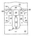
도 2a에서, p-타입 에피택시층 82가 고농도로 도핑된 n-타입 기판 80 위에 형성된다(예를 들면, 실리콘의 선택적인 에피택시 성장에 의함). 트랜치 84가 에피택시층 82 내의 중간의 깊이까지 식각된다. 제1 유전체층 86(예를 들면, 산화물을 포함함)이 트랜치 84의 측벽과 바닥을 덮고 트랜치 84에 인접한 실리콘 메사의 최상측 상에서 연장되도록 형성된다. 도면으로부터 알 수 있듯이, 상기 실리콘 메사 위에서 연장되는 상기 제1 유전체층 86의 일부가 트랜치 84 내부의 상기 제1 유전체층 86의 일부보다 더 두껍도록, 상기 제1 유전체층 86을 형성하는 것이 바람직하다. 상기 메사 영역 위의 보다 두꺼운 유전체를 획득하는 한가지 방법은, 예를 들면, 2006년 5월 24일자 출원되고 공동 양도된 미국 특허 출원 제11/441,386호의 도 13A 내지 13L에 도시된 것과 유사한 방식으로 ONO의 복합층을 형성하는 것이며, 상기 출원은 참조에 의해 그 전체가 본 명세서에 편입된다. 공지의 기술을 이용하여, 제2 유전체층(예를 들면, 질화물을 포함함)이 제1 유전체층 86 위에 형성되고, 유전체(예를 들면, 질화물) 스페이서 87을 형성하기 위해 식각된다.In FIG. 2A, a p-
도 2b에서, 유전체 스페이서 87이 보호 스페이서로서 기능하면서, 에피택시층 82가 트랜치 바닥을 따라 노출될 때까지 상기 제1 유전체층 86의 노출된 부분들이 식각된다. 상기 제1 유전체층 86이 상기 트랜치 바닥보다 상기 메사 영역 위에서 더 두꺼운 두께를 갖도록 형성된다면, 메사 표면은 상기 식각 후에도 (비록 더 얇지만) 상기 제1 실리콘층에 의해 덮인 상태로 유지된다.In FIG. 2B, while
도 2c에서, 실리콘 식각이 더 수행되고, 이로써 트랜치 84의 노출된 바닥면이 에피택시층 82를 완전히 통과해 기판 80 내로 연장되어 보다 깊은 트랜치 85가 형성된다. 따라서, 트랜치 85는 그 상부보다 더 좁은 하부를 포함한다. 상기 제1 유전체층 86 및 유전체 스페이서 87이 메사 표면 및 상측 트랜치 측벽을 보호하면서, 트랜치 85의 노출된 하측 측벽을 따라 n-타입 실리콘 영역 88을 형성하기 위해 n-타입 도펀트의 두 가지 경로의 경사진 주입 83이 수행된다. 도시된 바와 같이, n-타입 층 88은 기판 80과 합체된다. 유전체 스페이서 87은 상기 주입이 상기 채널 영역 내로 진입하는 것을 방지한다.In FIG. 2C, further silicon etching is performed, whereby the exposed bottom surface of
도 2e에서, 유전체 스페이스 87 및 제1 유전체층 86이 기존의 기술을 이용하여 제거된다. 실드 유전체 89 및 실드 전극 90이 기존의 기술을 이용하여 트랜치 85의 하부 내에 형성된다. 인터-폴리 유전체(inter-poly dielectric; IPD)층 92가 공지의 방법을 이용하여 실드 전극 90 위에 형성된다. 게이트 유전체 96 및 게이트 전극 94가 기존의 기술을 이용하여 IPD층 92 위에 형성된다. 소스 영역 93 및 고농도 본체 영역 95가 공지의 기술을 이용하여 형성된다. BPSG와 같은 유전체층 97이 게이트 94 및 소스 영역 93의 일부를 덮기 위해 상기 구조물의 최상측 위에 증착되고 패턴화되며, 소스 상호 접속층(도시되지 않음)이 소스 영역들 93 및 고농도 본체 영역들 95와 전기적으로 접속하도록 형성된다.In FIG. 2E,
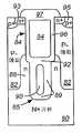
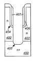
도 2a 내지 2e에 도시된 것과 유사한 처리가 p-타입 에피택시층이 아닌 n-타입 에피택시층 내에 실드 게이트 구조물을 형성하기 위해 수행될 수 있다. n-타입 도펀트의 두 가지 경로의 경사진 주입은 상기 채널 영역의 바닥부로의 본체 확산을 억제하는데, 이는 채널 저항을 감소시킨다는 점에서 유리하다. 이러한 주입은 또한 트랜치 측벽에서 나타나는 높은 전기장의 완화를 돕는다. 그러한 구조를 형성하는 바람직한 처리 흐름이 3a 내지 3e에 도시되어 있다. 도 3a에서, n-타입 에피택시층 402가 n-타입 기판 400 위에, 예를 들면, 선택적인 에피택시 성장을 이용하여 형성된다. 도 3e의 실드 게이트 구조물을 형성하게 하는 이후의 모든 단계들은, 도 3e에서, 소스 영역 413 및 고농도 본체 영역 415를 형성하기 이전에 p-타입 도펀트의 본체 주입이 본체 영역 418을 형성하기 위해 수행된다는 점을 제외하고는 도 2a 내지 2e에서의 대응 단계들과 유사하다. 도 3d 및 3e로부터 알 수 있듯이, 두 가지 경로의 경사진 주입에 의해 형성된 실리콘 영역 408은 채널 영역 내로 확산되고, 이로써 채널 저항을 감소시킨다.Processing similar to that shown in FIGS. 2A-2E may be performed to form the shield gate structure in the n-type epitaxy layer but not the p-type epitaxy layer. Inclined injection of two paths of n-type dopant inhibits body diffusion into the bottom of the channel region, which is advantageous in that it reduces channel resistance. This injection also helps to alleviate the high electric fields that appear in the trench sidewalls. Preferred process flows for forming such a structure are shown in 3a to 3e. In FIG. 3A, an n-
본 발명의 다른 실시예에 따르면, 전하 균형 실드 게이트 MOSFET이 n-타입 에피택시층 및 에피택시적으로 성장된 p-타입 실리콘으로 채워지는 깊은 딤플(dimple)을 이용하여 형성된다. 이러한 실시예가 도 4의 바람직한 단면도를 이용하여 설명될 것이다. 도 4에서, 모든 두 개의 게이트 트랜치들 131 사이에서, 깊은 딤플 133이 본체 영역 136 및 n-타입 에피택시층 132를 통해 연장되고 고농도로 도핑된 n-타입 기판 130 내에서 종단된다. 딤플 133은 p-타입 실리콘 물질 134로 채워진다. n-타입 에피택시층 132 및 딤플 133 내의 실리콘 물질 134의 도핑 농도는 이들 두 영역 사이에서 전하 균형이 획득되도록 선택된다. 그 외의 게이트 트랜치 구조는 이전의 실시예들와 유사하므로, 설명이 생략될 것이다.According to another embodiment of the present invention, a charge balanced shield gate MOSFET is formed using a deep dimple filled with an n-type epitaxy layer and epitaxially grown p-type silicon. This embodiment will be described using the preferred cross section of FIG. In FIG. 4, between all two
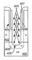
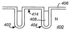
도 4의 상기 구조를 형성하는 방법의 예시는 이하와 같다. n-타입 에피택시층 132가 고농도로 도핑된 n-타입 기판 130 위에 형성된다(예를 들면, 선택적인 에피택시 성장에 의함). p-타입 도전성의 본체 영역 136이 에피택시층 132 내로 도펀트를 주입함으로써 형성된다. 본체 영역 136이 채널 영역을 형성할 만큼의 깊이까지 연장된다. 그 후 실리콘 식각이, 본체 영역 136을 통해 연장되고 기판 130 내에서 종단되는 깊은 딤플 133을 형성하기 위해 수행된다. 선택적인 에피택시 성장 처리가 깊은 딤플 133을 p-타입 실리콘 134로 채우기 위해 행해진다. 게이트 트랜치 131과 그 내부의 다양한 물질들은 물론, 소스 영역 140, 고농도 본체 영역 138 및 다른 구조적 형상들이 공지의 기술에 따라 형성된다. 일 실시예에서는 게이트 트랜치 및 게이트와 실드 전극이 상기 깊은 딤플이 형성되기 전에 형성된다. 딤플 133을 기판-에피택시층의 경계 아래로 연장시킴으로써, 필러(pillar)의 바닥에서의 높은 전기장이 완화된다는 점에서 유리하다. 이는 보다 얇은 n-타입 에피택시층을 가능하게 하여 온-상태 저항을 감소시킨다.An example of a method of forming the structure of FIG. 4 is as follows. An n-
도 5a 및 5b는 도 4의 깊은 p-타입 영역 134를 형성하는 다른 방법을 도시한다. 도 5a 및 5b에 도시된 바와 같이, p-타입 필러 164가 얕은 딤플 168을 통해 n-타입 에피택시층 162 내로 p-타입 도펀트의 다수의 고에너지 주입 172를 수행함으로써 형성된다. 도시된 바와 같이, 상기 딤플의 깊이는 다른 소스 영역들 166의 것보다 조금 더 깊다. 주입 172는 딤플 168의 바닥면 내로 행해지므로, 상기 딤플의 깊이는 p-타입 필러의 깊이에 대한 기준점을 설정한다. 상기 주입 172의 분량 및 에너지는 p-타입 필러 164 내의 요구된 도핑 프로파일을 획득하도록 조정될 수 있다. 상기 처리의 종료시 확산이 매우 적게 일어나므로, 최종 p-타입 필러 164 및 n-타입 에피택시층 162 모두의 도핑 프로파일은 상대적으로 편평하다. 이로써 처리 감도가 개선된다.5A and 5B illustrate another method of forming the deep p-
본 발명의 다른 실시예에 따르면, 전하 균형 MOSFET(특히 저전압 응용 제품에 이용되지만 이에 한정되지는 않음)에 대한 추가적 방법 및 구조들은 게이트 트랜치들 사이에 비-게이트(non-gated) 실드 트랜치를 이용한다. 이러한 실시예들이 이하에 기재되어 있다.According to another embodiment of the present invention, additional methods and structures for charge balanced MOSFETs (particularly, but not limited to, low voltage applications) use non-gated shield trenches between the gate trenches. . These embodiments are described below.
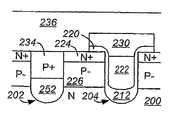
기존의 트랜치 게이트 FET보다 높은 항복 전압을 획득하기 위하여 드레인-소스 간 높은 역 바이어스(reverse bias) 하에서의 고갈(depletion)을 제어하기 위해, 전하 균형 트랜치 게이트 FET는 메사의 폭과 드리프트 영역(전형적으로, 에피택시층임)의 도핑 농도에 의존한다. 메사의 폭은, 인접한 게이트 트랜치들 사이의 메사의 중앙에 연속된 고농도 본체 접촉 영역을 정의하기 위한 포토리소그라피의 성능에 의해 제한된다. 그러나, 본 발명의 일 실시예에 따르면, 게이트 트랜치들 사이에 산재된 추가적인 비-게이트 실드 트랜치의 사용에 의해 동일한 항복 전압에 대한 드리프트 영역 저항성을 감소시키고, 효율적으로 디바이스의 온-상태를 약화시키며, 개선된 전하 균형 특성을 달성할 수 있다.To control the depletion under high reverse bias between drain and source to obtain higher breakdown voltages than conventional trench gate FETs, charge balanced trench gate FETs are typically designed for mesa widths and drift regions (typically, Depending on the doping concentration of the epitaxy layer). The width of the mesa is limited by the ability of photolithography to define a continuous high concentration body contact area in the center of the mesa between adjacent gate trenches. However, according to one embodiment of the present invention, the use of additional non-gate shield trenches interspersed between the gate trenches reduces drift region resistance to the same breakdown voltage and effectively weakens the on-state of the device. Thus, improved charge balance characteristics can be achieved.
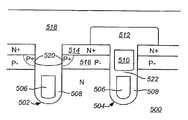
도 6a 내지 6g는 본 발명의 일 실시예에 따른, 게이트 트랜치들 사이에 편입된 자기 정렬된 비-게이트 트랜치를 포함하는 트랜치 게이트 FET를 형성하는 바람직한 처리 흐름을 도시하는 단순화된 단면도이다. 도 6a에서, 기존의 기술을 이용하여, 트랜치 202 및 204가 실리콘 영역 200 내로 식각된다. 일 실시예에서, 실리콘 영역 200은 고농도로 도핑된 n-타입 기판 및 상기 기판 위의 n-타입 에피택시층을 포함한다.6A-6G are simplified cross-sectional views illustrating a preferred process flow for forming a trench gate FET that includes self-aligned non-gate trenches incorporated between gate trenches, in accordance with one embodiment of the present invention. In FIG. 6A, using conventional techniques,
트랜치 202는 비-게이트 트랜치라고 할 것이고, 트랜치 204는 게이트 트랜치라고 할 것이다. 메사 표면 208 위에서 연장되고 트랜치 202 및 204의 측벽과 바닥면을 덮는 유전체층 206(예를 들면, 성장된 산화물임)이 공지의 기술을 이용하여 형성된다. 도 6b에서, 상기 트랜치들을 채우고 상기 메사 영역 위에서 연장되는 유전체 물질 210(예를 들면, SACVD와 같은 증착된 박막임)이 기존의 방법을 이용하여 증착된다. 도 6c에서, 상기 트랜치들 내에 잔존하는 상기 유전체 물질 210의 최상면이 메사 표면 208과 실질적으로 동일 평면상에 존재하도록, 평탄화 처리가 공지의 기술을 이용하여 수행된다.Trench 202 will be referred to as a non-gate trench and
도 6d에서, 기존의 방법을 이용하여, 마스크층(예를 들면, 포토레지스트)이 비-게이트 트랜치 202를 덮는 마스크 영역 214를 형성하기 위해 증착되고 패턴화되며, 게이트 유전체 204의 바닥을 따라 두꺼운 바닥측 유전체(thick bottom dielectric; TBD) 212를 형성하기 위해, 게이트 트랜치 204 내의 유전체층 206 및 유전체 물질 210이 우묵하게 된다(recessed). 도 6e에서, 마스크 영역 214가 제거되고, 게이트 트랜치 204의 측벽을 덮고 메사 표면과 비-게이트 트랜치 202 위에서 연장되는 게이트 유전체층 220(예를 들면, 산화물을 포함함)이 기존의 기술을 이용하여 형성된다. 게이트 트랜치 204 내에 리세스(recessed) 게이트 전극 222를 형성하기 위해, 폴리실리콘층이 증착되고 게이트 트랜치 204 내로 우묵하게 된다. 순차적으로, 실리콘 영역 200 내에 p-타입 본체 영역 226을 형성하고 본체 영역 226 내에 고농도로 도핑된 n-타입 소스 영역을 형성하기 위해, 기존의 블랭킷 본체 및 소스 주입이 디바이스의 활성 영역에서 수행된다.In FIG. 6D, using a conventional method, a mask layer (eg, photoresist) is deposited and patterned to form a
도 6f에서, 공지의 기술을 이용하여, 게이트 트랜치 204 위에서만 연장되는 유전체 캡(cap) 230을 형성하기 위해, 유전체층(예를 들면, BPSG를 포함함)이 상기 구조물 위에 형성되고, 패턴화 및 식각된다. 비-게이트 트랜치 202 내의 유전체 물질 206 및 210을 본체 영역 226의 측벽을 부분적으로 노출시킬 만큼 우묵하게 하기 위해, 동일한 유전체 식각이 사용될 수 있다. 따라서, 유전체 영역 252가 비-게이트 트랜치 202의 바닥을 따라 잔존한다.In FIG. 6F, using a known technique, a dielectric layer (including, for example, BPSG) is formed over the structure to form a
도 6g에서, 비-게이트 트랜치 202가 고농도 본체 영역 234를 형성하기 위해 도전성 물질(예를 들면, 고농도로 도핑된 p-타입 폴리실리콘)로 채워진다. 소스 상호 접속층 236(예를 들면, 금속을 포함함)이 소스 영역들 224 및 고농도 본체 영역들 234와 접속하도록 상기 구조물 위에 형성된다. 일 실시예에서는 고농도 본체 영역 234를 형성함에 있어서, 소스 영역 224의 측벽을 부분적으로 노출시키기 위하여, 증착된 상기 도전성 물질이 비-게이트 트랜치 202 내로 우묵하게 된다. 이는 소스 상호 접속층 230이 소스 영역 224의 측벽과 직접 접속할 수 있도록 하여, 소스 접속 저항을 감소시킨다.In FIG. 6G,
도면으로부터 알 수 있듯이, 소스 영역 224는 상기 트랜치들에 자기 정렬된다. 스트라이프(stripe) 형태의 셀 구조가 사용되는 일 실시예에서는, 도 6a 내지 6g에서 도시된 상기 처리 시퀀스가, 역시 자기 정렬되는 연속된 고농도 본체 영역 234를 형성하도록 한다. 최종 구조물의 이들 및 다른 자기 정렬된 형상들은 매우 조밀한 셀 피치를 달성하게 한다. 또한, 상기 소스 및 고농도 본체 영역의 각각을 형성함에 있어서 전형적으로 요구되는 마스크 단계가 제거되고, 이로써 비용이 감소되고 처리 복잡도가 최소화된다.As can be seen from the figure, the
일 실시예에서, 하나의 비-게이트 트랜치가 모든 두 개의 게이트 트랜치들 사이에 형성된다. 다른 실시예에서, 게이트-드레인 용량을 감소시키기 위해 게이트 트랜치에 대한 비-게이트 트랜치의 보다 큰 비율이 사용된다(예를 들면, 두 개 또는 그 이상의 비-게이트 트랜치가 모든 두 개의 게이트 트랜치들 사이에 형성됨). 또 다른 실시예에서는, 비-게이트 및 게이트 트랜치를 동시에 형성하는 대신, 비-게이트 트랜치가 게이트 트랜치와 다른 처리 단계에서 형성된다. 이는 추가적인 처리 단계를 야기하는 한편, 이러한 실시예는 처리 및 구조의 다양한 특징을 최적화함에 있어서 유연성을 제공한다.In one embodiment, one non-gate trench is formed between all two gate trenches. In other embodiments, a larger ratio of non-gate trenches to gate trenches is used to reduce gate-drain capacity (e.g., two or more non-gate trenches between all two gate trenches). Formed on). In another embodiment, instead of forming the non-gate and gate trenches simultaneously, the non-gate trenches are formed in different processing steps than the gate trenches. This results in additional processing steps, while this embodiment provides flexibility in optimizing various features of the processing and structure.
도 7a 내지 7h는 본 발명의 일 실시예에 따른, 게이트 트랜치들 사이에 편입된 자기 정렬된 비-게이트 트랜치를 포함하는 실드 게이트 FET를 형성하는 다른 바람직한 처리 흐름을 도시하는 단순화된 단면도이다. 도 7a에서, 게이트 트랜치 304 및 비-게이트 트랜치 302가 n-타입 실리콘 영역 300 내로 식각된다. 일 실시예에서, 실리콘 영역 300은 고농도로 도핑된 n-타입 기판 및 상기 기판 위의 n-타입 에피택시층을 포함한다. 이러한 실시예의 일 변형례에서는 트랜치 302 및 304가 상기 에피택시층 내에서 종단되고, 다른 변형례에서는 트랜치 320 및 304가 상기 에피택시층을 통해 연장되고 상기 기판 내에서 종단된다.7A-7H are simplified cross-sectional views illustrating another preferred process flow for forming a shield gate FET that includes a self-aligned non-gate trench incorporated between gate trenches, in accordance with an embodiment of the present invention. In FIG. 7A,
도 7a에서, 메사 표면 308 위에서 연장되고 트랜치 302 및 304의 측벽 및 바닥면을 덮는 실드 유전체층 306(예를 들면, 산화물을 포함함)이 공지의 기술을 이용하여 형성된다. 트랜치 302 및 304 내에 실드 전극 310을 형성하기 위해, 폴리실리콘층이 기존의 기술을 이용하여 증착되고 트랜치 302 및 304 내로 깊이 우묵하게 된다. 도 7b에서, 상기 트랜치들을 채우고 상기 메사 영역 위에서 연장되는 유전체 물질 312(예를 들면, SACVD를 이용하는 증착된 박막)가 기존의 방법을 이용하여 증착된다. 도 7c에서, 상기 트랜치 내에 잔존하는 유전체 물질 312의 최상면이 메사 표면 308과 실질적으로 동일 평면상에 존재하도록, 공지의 기술을 이용하여 평탄화 처리가 수행된다.In FIG. 7A, a shield dielectric layer 306 (including, for example, oxide) that extends over the
도 7d에서, 기존의 방법을 이용하여, 비-게이트 트랜치 302를 덮는 마스크 영역 314를 형성하기 위해 마스크층(예를 들면, 포토레지스트)이 증착되고 패턴화되며, 실드 전극 310 위에 전극 간 유전체 316(inter-electrode dielectric; IED)을 형성하기 위해, 게이트 트랜치 304 내의 유전체층 306 및 유전체 물질 312가 미리 정해진 깊이까지 우묵하게 된다. 도 7e에서, 마스크 영역 314가 제거되고, 게이트 트랜치 304의 상측 측벽을 덮고 메사 표면 및 비-게이트 트랜치 302 위에서 연장되는 게이트 유전체층 322(예를 들면, 산화물을 포함함)가 기존의 기술을 이용하여 형성된다. 게이트 트랜치 304 내에 리세스 게이트 전극 324를 형성하기 위해, 폴리실리콘층이 증착되고 게이트 트랜치 304 내로 우묵하게 된다. 도 7f에서, 실리콘 영역 300 내에 p-타입 본체 영역 328을 형성하고, 본체 영역 328 내에 고농도로 도핑된 n-타입 소스 영역 326을 형성하기 위해, 기존의 블랭킷 본체 및 소스 주입이 본 디바이스의 활성 영역에서 순차적으로 수행된다.In FIG. 7D, using an existing method, a mask layer (eg, photoresist) is deposited and patterned to form a
도 7g에서, 게이트 트랜치 304 위에 유전체 캡 330을 형성하기 위해, 공지의 기술을 이용하여 유전체층(예를 들면, BPSG를 포함함)이 상기 구조물 위에 형성되고 패턴화 및 식각된다. 비-게이트 트랜치 302 내의 유전체 물질 306 및 310을 본체 영역 328의 측벽을 부분적으로 노출시킬 만큼 우묵하게 하기 위해, 동일한 유전체 식각이 사용될 수 있다. 따라서, 유전체 물질 325가 비-게이트 트랜치 302 내에 실드 전극 310 위에 잔존한다. 비-게이트 트랜치 302가 고농도 본체 영역 332를 형성하기 위해 도전성 물질(예를 들면, 고농도로 도핑된 p-타입 폴리실리콘)로 채워진다. 소스 상호 접속층 334(예를 들면, 금속을 포함함)가 소스 영역들 326 및 고농도 본체 영역들 332와 접속하도록, 상기 구조물 위에 형성된다. 일 실시예에서는 고농도 본체 영역 332를 형성함에 있어서, 소스 영역 326의 측벽을 부분적으로 노출시키기 위하여, 증착된 상기 도전성 물질이 비-게이트 트랜치 302 내로 우묵하게 된다. 이는 소스 상호 접속층 334가 소스 영역 326의 측벽과 직접 접속할 수 있도록 하여, 소스 접속 저항을 감소시킨다.In FIG. 7G, to form
이전의 실시예에서와 같이, 소스 영역 326은 상기 트랜치들에 자기 정렬되고, 스트라이프 형태의 셀 구조가 사용되는 일 실시예에서는, 도 7a 내지 7h에서 도시된 상기 처리 시퀀스가, 역시 자기 정렬되는 연속된 고농도 본체 영역 332를 형성하게 한다. 최종 구조물의 이들 및 다른 자기 정렬된 형상들은 매우 조밀한 셀 피치를 달성하게 한다. 또한, 상기 비-게이트 트랜치 내의 실드 전극은 동일한 항복 전압에 대해 드리프트 영역 저항이 감소될 수 있도록 한다. 또한, 상기 소스 및 고농도 본체 영역의 각각을 형성함에 있어서 전형적으로 요구되는 마스크 단계가 제거되고, 이로써 비용이 감소되고 처리 복잡도가 최소화된다.As in the previous embodiment, the
상기 게이트 및 비-게이트 트랜치 내의 실드 전극들은 제3차원에서 상기 소스 상호 접속층에 전기적으로 접속될 수 있고, 또는 부유(floating)하게 될 수도 있다. 일 실시예에서, 하나의 비-게이트 트랜치가 모든 두 개의 게이트 트랜치들 사이에 형성된다. 다른 실시예에서, 게이트-드레인 용량을 감소시키기 위해 게이트 실드 트랜치에 대한 비-게이트 트랜치의 보다 큰 비율이 사용된다(예를 들면, 두 개 또는 그 이상의 비-게이트 트랜치가 모든 두 개의 게이트 트랜치들 사이에 형성됨). 또 다른 실시예에서는, 비-게이트 및 게이트 트랜치를 동시에 형성하는 대신, 비-게이트 트랜치가 게이트 트랜치와 다른 처리 단계에서 형성된다. 이는 추가적인 처리 단계를 야기하는 한편, 이러한 실시예는 처리 및 구조의 다양한 특징을 최적화함에 있어서 유연성을 제공한다.Shield electrodes in the gate and non-gate trenches may be electrically connected to the source interconnect layer in a third dimension, or may be floating. In one embodiment, one non-gate trench is formed between all two gate trenches. In another embodiment, a larger ratio of non-gate trench to gate shield trench is used to reduce the gate-drain capacity (e.g., two or more non-gate trenches are used for all two gate trenches). Formed between). In another embodiment, instead of forming the non-gate and gate trenches simultaneously, the non-gate trenches are formed in different processing steps than the gate trenches. This results in additional processing steps, while this embodiment provides flexibility in optimizing various features of the processing and structure.
도 8a 내지 8h는 본 발명의 다른 실시예에 따른, 게이트 트랜치들 사이에 편입된 자기 정렬된 비-게이트 트랜치를 포함하는 실드 게이트 FET를 형성하는 또 다른 바람직한 처리 흐름을 도시하는 단순화된 단면도이다. 도 8a에서, 게이트 트랜치 404 및 비-게이트 트랜치 402가 n-타입 실리콘 영역 400 내로 식각된다. 일 실시예에서, 실리콘 영역 400은 고농도로 도핑된 n-타입 기판 및 상기 기판 위의 n-타입 에피택시층을 포함한다. 이러한 실시예의 일 변형례에서는 트랜치 402 및 404가 상기 에피택시층 내에서 종단되고, 다른 변형례에서는 트랜치 402 및 404가 상기 에피택시층을 통해 연장되고 상기 기판 내에서 종단된다.8A-8H are simplified cross-sectional views illustrating another preferred process flow for forming a shield gate FET that includes self-aligned non-gate trenches incorporated between gate trenches, in accordance with another embodiment of the present invention. In FIG. 8A,
도 8a에서, 메사 표면 414 위에서 연장되고 트랜치 402 및 404의 측벽 및 바닥면을 덮는 실드 유전체층 406(예를 들면, 산화물을 포함함)이 공지의 기술을 이용하여 형성된다. 도시된 바와 같이, 폴리실리콘층이 증착되고 실드 유전체층 406의 최상면의 조금 아래로 에치-백(etch-back)된다. 도 8b에서, 기존의 방법을 이용하여, 비-게이트 트랜치 402를 덮는 마스크 영역 412를 형성하기 위해 마스크층(예를 들면, 포토레지스트)이 증착되고 패턴화된다. 도 8c에서, 게이트 트랜치 404에 실드 전극 410을 형성하기 위해 게이트 트랜치 404 내의 폴리실리콘 410이 상기 트랜치 내로 깊이 우묵하게 된다. 도시된 바와 같이, 마스크 영역 412가 제거되고 실드 유전체층 406이 에치-백 된다.In FIG. 8A, a shield dielectric layer 406 (eg including oxide) is formed using known techniques that extend over the
도 8d에서, 게이트 트랜치 404의 상측 측벽을 덮고 실드 전극 410, 메사 표면 및 비-게이트 트랜치 402 위에서 연장되는 게이트 유전체층 420(예를 들면, 산화물을 포함함)이 기존의 기술을 이용하여 성장된다. 게이트 트랜치 404 내에 리세스 게이트 전극 418을 형성하기 위해, 폴리실리콘층이 증착되고 게이트 트랜치 404 내로 우묵하게 된다. 도 8e에서, 실리콘 영역 400 내에 p-타입 본체 영역 424를 형성하고, 본체 영역 424 내에 고농도로 도핑된 n-타입 소스 영역 422를 형성하기 위해, 기존의 블랭킷 본체 및 소스 주입이 본 디바이스의 활성 영역에서 수행된다.In FIG. 8D, a gate dielectric layer 420 (including oxides) covering the upper sidewalls of the
도 8f에서, 게이트 트랜치 404 위에 유전체 캡 426을 형성하기 위해, 공지의 기술을 이용하여 유전체층(예를 들면, BPSG를 포함함)이 상기 구조물 위에 형성되고 패턴화 및 식각된다. 비-게이트 트랜치 402 내의 실드 유전체 406을 본체 영역 424의 측벽을 부분적으로 노출시킬 만큼 우묵하게 하기 위해, 동일한 유전체 식각이 사용될 수 있다. 도 8g에서, 도전성 물질(예를 들면, 고농도로 도핑된 p-타입 폴리실리콘)이 비-게이트 트랜치 402를 채우기 위해 증착되고 에치-백되어, 비-게이트 트랜치 402 내에 고농도 본체 영역 430을 형성한다. 도 8h에서, 소스 상호 접속층 432(예를 들면, 금속을 포함함)가 소스 영역들 422 및 고농도 본체 영역들 430과 접속하도록, 상기 구조물 위에 형성된다.In FIG. 8F, to form
도면으로부터 알 수 있듯이, 소스 영역 422는 상기 트랜치들에 자기 정렬된다. 스트라이프 형태의 셀 구조가 사용되는 실시예에서는, 도 8a 내지 8h에 도시된 상기 처리 시퀀스가, 역시 자기 정렬되는 연속된 고농도 본체 영역 430을 형성하게 한다. 최종 구조물의 이들 및 다른 자기 정렬된 형상들은 매우 조밀한 셀 피치를 달성하게 한다. 또한, 상기 비-게이트 트랜치 내의 실드 전극은 항복 전압을 저하시키지 않으면서 드리프트 영역 저항성이 감소될 수 있도록 한다. 또한, 상기 소스 및 고농도 본체 영역의 각각을 형성함에 있어서 전형적으로 요구되는 마스크 단계가 제거되고, 이로써 비용이 감소되고 처리 복잡도가 최소화된다.As can be seen from the figure,
도면으로부터 알 수 있듯이, 비-게이트 트랜치 402 내의 실드 전극 408은 고농도 본체 영역 430을 거쳐 소스 상호 접속부 432에 전기적으로 접속된다. 일 실시예에서, 하나의 비-게이트 트랜치가 모든 두 개의 게이트 트랜치들 사이에 형성된다. 다른 실시예에서, 게이트-드레인 용량을 감소시키기 위해 게이트 실드 트랜치에 대한 비-게이트 트랜치의 보다 큰 비율이 사용된다(예를 들면, 두 개 또는 그 이상의 비-게이트 트랜치가 모든 두 개의 게이트 트랜치들 사이에 형성됨). 또 다른 실시예에서는, 비-게이트 및 게이트 트랜치를 동시에 형성하는 대신, 비-게이트 트랜치가 게이트 트랜치와 다른 처리 단계에서 형성된다. 이는 추가적인 처리 단계를 야기하는 한편, 이러한 실시예는 처리 및 구조의 다양한 특징을 최적화함에 있어서 유연성을 제공한다.As can be seen from the figure, the
도 9는 고농도 본체 영역이 비-게이트 트랜치 내부가 아닌 본체 영역 내에 형성되는, 비-게이트 트랜치를 포함하는 실드 게이트 FET의 단순화된 단면도이다. 고농도 본체 영역 520이 본체 영역 516 내에 형성되고, 소스 상호 접속층 518이 비-게이트 트랜치 502의 상부 내로 연장되고 상기 비-게이트 트랜치 502의 상부를 채운다는 점을 제외하고는, 도 9의 실드 게이트 FET 구조는 도 7h의 것과 유사하다. 도시된 바와 같이, 소스 상호 접속층은 소스 영역 514와 메사 표면 및 상기 소스 영역의 측벽을 따라 전기적으로 접속하고, 고농도 본체 영역 520과 그 측벽을 따라 접속한다. 도 9의 상기 FET의 나머지 구조적 특징은 도 7h의 것들과 유사하므로, 설명되지 않을 것이다.9 is a simplified cross-sectional view of a shield gate FET that includes a non-gate trench, in which a high concentration body region is formed within the body region rather than inside the non-gate trench. The shield gate of FIG. 9 except that a high
도 9의 FET 구조물을 형성하는 처리 흐름은 이하의 변경 사항들을 제외하고는 도 7a 내지 7h에 도시된 것들과 유사하다. 도 7g에서, 비-게이트 트랜치 302 내의 유전체 물질 306 및 310을 우묵하게 하여 본체 영역 328의 측벽이 부분적으로 노출된 후, 비-게이트 트랜치 302의 노출된 측벽들로의 p-타입 도펀트의 두 가지 경로의 경사진 주입이, 본체 영역 내에 고농도 본체 영역 520(도 9)을 형성하기 위해 수행된다. 일 실시예에서, 상기 두 가지 경로의 경사진 주입을 수행함에 있어서 마스크가 사용되지 않고, 상기 비-게이트 트랜치 부근에서의 상기 소스 영역들의 유효한 도핑 농도가 상기 고농도 본체 주입에 의해 어떠한 유의미한 영향도 받지 않도록, 상기 고농도 본체 주입 분량이 소스 영역들보다 낮게 선택된다.The process flow forming the FET structure of FIG. 9 is similar to those shown in FIGS. 7A-7H except for the following changes. In FIG. 7G, two portions of the p-type dopant to the exposed sidewalls of the
도 7h에서, 상기 구조물 위에 소스 상호 접속층을 증착할 때 상기 소스 상호 접속층은 비-게이트 트랜치를 채우므로, 도 9에 도시된 바와 같이, 상기 고농도 본체 영역들 및 상기 소스 영역들과, 그들의 측벽을 따라 전기적으로 접속한다. 도 9의 실시예는 상기한 도 7h에서 도시된 실시예들과 동일한 특징 및 이점을 갖는다. 또한, 상기한 도 7a 내지 7h의 실시예들에 대한 대체적 변형례 및 실시예들이 도 9의 FET 구조에도 적용된다.In FIG. 7H, when depositing a source interconnect layer over the structure, the source interconnect layer fills a non-gate trench, so as shown in FIG. 9, the high concentration body regions and the source regions and their Electrically connect along the sidewalls. The embodiment of FIG. 9 has the same features and advantages as the embodiments shown in FIG. 7H described above. In addition, alternative variations and embodiments of the embodiments of FIGS. 7A-7H described above also apply to the FET structure of FIG. 9.
도 10은 상기 고농도 본체 영역이 상기 비-게이트 트랜치 내부가 아닌 본체 영역 내에 형성되는, 비-게이트 트랜치를 포함하는 트랜치 게이트 FET의 단순화된 단면도이다. 고농도 본체 영역 620이 본체 영역 618 내에 형성되고 소스 상호 접속층 622가 비-게이트 트랜치 602의 상부 내로 연장되고 상기 비-게이트 트랜치 602의 상부를 채운다는 점을 제외하고는, 도 10의 트랜치 게이트 FET 구조는 도 6g의 것과 유사하다. 도시된 바와 같이, 소스 상호 접속층은 소스 영역 514와 메사 표면 및 상기 소스 영역의 측벽을 따라 전기적으로 접속하고, 고농도 본체 영역 520과 그 측벽을 따라 접속한다. 도 10의 상기 FET의 나머지 구조적 특징은 도 6g의 것들과 유사하므로, 설명되지 않을 것이다.FIG. 10 is a simplified cross-sectional view of a trench gate FET including a non-gate trench, wherein the heavily doped body region is formed within the body region rather than inside the non-gate trench. The trench gate FET of FIG. 10, except that a high concentration body region 620 is formed within the
도 10의 FET 구조를 형성하는 처리 흐름은 이하의 변경 사항들을 제외하고는 도 6a 내지 6g에서 도시된 것들과 유사하다. 도 6f에서, 비-게이트 트랜치 202 내의 유전체 물질 206 및 210을 우묵하게 하여 본체 영역 226의 측벽이 부분적으로 노출된 후, 비-게이트 트랜치 202의 노출된 측벽들로의 p-타입 도펀트의 두 가지 경로의 경사진 주입이 상기 본체 영역 내에 고농도 본체 영역 620(도 10)을 형성하기 위해 수행된다. 일 실시예에서, 상기 두 가지 경로의 경사진 주입을 수행함에 있어서 마스크가 사용되지 않고, 상기 비-게이트 트랜치 부근에서의 상기 소스 영역들의 유효한 도핑 농도가 상기 고농도 본체 주입에 의해 어떠한 유의미한 영향도 받지 않도록, 상기 고농도 본체 주입 분량이 소스 영역들보다 낮게 선택된다.The process flow forming the FET structure of FIG. 10 is similar to those shown in FIGS. 6A-6G with the following changes. In FIG. 6F, two portions of the p-type dopant to the exposed sidewalls of the
도 6g에서, 상기 구조물 위에 소스 상호 접속층을 증착할 때 상기 소스 상호 접속층은 비-게이트 트랜치를 채우므로, 도 10에 도시된 바와 같이, 상기 고농도 본체 영역들 및 상기 소스 영역들과, 그들의 측벽을 따라 전기적으로 접속한다. 도 10의 실시예는 상기한 도 6g에서 도시된 실시예들과 동일한 특징 및 이점을 갖는다. 또한, 상기한 도 6a 내지 6g의 실시예들에 대한 대체적 변형례 및 실시예들이 도 10의 FET 구조에도 적용된다.In FIG. 6G, when depositing a source interconnect layer over the structure, the source interconnect layer fills a non-gate trench, so that the high concentration body regions and the source regions, as shown in FIG. Electrically connect along the sidewalls. The embodiment of FIG. 10 has the same features and advantages as the embodiments shown in FIG. 6G described above. In addition, alternative variations and embodiments to the embodiments of FIGS. 6A-6G described above also apply to the FET structure of FIG. 10.
본 발명의 다양한 구조 및 방법이, 다른 이점들 및 특징들 가운데 더욱더 낮은 온-저항, 보다 높은 차단(blocking) 성능 및 보다 높은 효율을 달성하기 위해, 2004년 12월 29일자로 출원되고 참조를 통해 그 전체가 본 명세서에 편입된 공동 양도된 미국 출원 제11/026,276호에서 개시된, 다수의 전하 균형 및 실드 게이트 기술들(예를 들면, 도 2A 및 2B, 3A 및 3B, 4A 내지 4E, 5B 및 5C, 6 내지 8, 9A 내지 9C, 10 내지 24의 것들)은 물론, 다른 디바이스 구조물 및 제조 처리들 중 하나 또는 그 이상의 것과 결합될 수 있다. 또한, 최적화된 성능 및 구조적 특성을 갖는 전하 균형 실드 게이트 디바이스를 획득하기 위해, 상기 참조된, 공동 양도된 2006년 5월 24일자 미국 특허 출원 제11/441,386호에 개시된 다양한 실드 게이트 구조들(예를 들면, 도 4 내지 7의 것들) 및 그 형성 방법들 중 하나 또는 그 이상이 본 명세서에 개시된 전하 균형 기술들(예를 들면, 도 3a 내지 3e, 4, 5a 및 5b, 7a 내지 7h, 8a 내지 8h, 9 및 10) 중 하나 또는 그 이상과 결합될 수 있다는 점에서 유리하다.Various structures and methods of the present invention are filed on December 29, 2004 and incorporated by reference to achieve lower on-resistance, higher blocking performance and higher efficiency, among other advantages and features. A number of charge balance and shield gate techniques (e.g., FIGS. 2A and 2B, 3A and 3B, 4A to 4E, 5B, and those disclosed in commonly assigned US application Ser. No. 11 / 026,276, incorporated herein in its entirety) 5C, 6-8, 9A-9C, 10-24) as well as one or more of other device structures and fabrication processes. In addition, various shield gate structures disclosed in US Patent Application No. 11 / 441,386, issued May 24, 2006, referenced above, to obtain a charge balanced shield gate device having optimized performance and structural characteristics (e.g., For example, one or more of those of FIGS. 4-7 and methods of forming the same may be described in the charge balancing techniques disclosed herein (eg, FIGS. 3A-3E, 4, 5A and 5B, 7A-7H, 8A). To 8h, 9 and 10) in that it is advantageous in that it can be combined.
본 명세서에 기재된 서로 다른 실시예들의 단면도들은 같은 비율로 축적되어 있지 않을 수 있고, 그 자체가 가능한 변형례들을 대응하는 구조들의 구성 설계 내로 제한하도록 의도된 것이 아니다.The cross-sectional views of the different embodiments described herein may not be accumulated in the same proportions, and are not intended to limit the possible variations by themselves into the constructional design of the corresponding structures.
다수의 특정 실시예들이 도시되고 상기 기재되었지만, 본 발명의 실시예들은 그에 한정되지 않는다. 예를 들면, 상기한 다양한 실시예들이 기존의 실리콘에 구현되어 있지만, 이러한 실시예들 및 이들의 자명한 변형례들은 또한 실리콘 카바이드(silicon carbide), 갈륨 비화물(gallium arsenide), 갈륨 질화물(gallium nitride) 또는 다른 반도체 물질에 구현될 수 있다. 다른 실시예에서는, 상기 실시예들이 n-채널 트랜지스터의 맥락에서 기재된 한편, p-채널의 대응 트랜지스터가 단순히 다양한 영역들의 도전성 타입을 역전시킴으로써 형성될 수 있다. 또한, 본 명세서에 기재된 다양한 트랜지스터는, 6방 정계형, 타원형 또는 사각형 모양의 셀을 포함하는 개방형 또는 폐쇄형 셀 구조로 형성될 수 있다. 나아가, 본 발명의 실시예들은 MOSFET에 한정되지 않는다. 예를 들면, 상기한 MOSFET의 IGBT 대응물을 형성하기 위해 필요한 변경은 본 개시의 관점에서 본 발명이 속하는 기술 분야에서 통상의 지식을 자긴 자에게 자명할 것이다. 또한, 본 명세서에 기재된 소정의 실시예들은 저전압 응용 제품에 특히 유용한 한편, 고전력 응용 제품에 보다 적합하며 본 발명과 동일한 이점들 및 특징들 중 많은 것들을 갖는 트랜지스터를 형성하기 위해, 본 명세서에 기재된 처리 흐름 및 구조가 본 개시의 관점에서 본 발명이 속하는 기술 분야에서 통상의 지식을 가진 자에 의해 수정될 수 있다. 나아가, 본 발명의 하나 또는 그 이상의 실시예들의 특징은 본 발명의 범위로부터 벗어나지 아니한 채 본 발명의 다른 실시예들의 하나 또는 그 이상의 특징들과 결합될 수 있다.While a number of specific embodiments have been shown and described above, embodiments of the invention are not so limited. For example, while the various embodiments described above are implemented in conventional silicon, these embodiments and their obvious variations are also silicon carbide, gallium arsenide, gallium nitride. nitride) or other semiconductor material. In other embodiments, while the above embodiments are described in the context of n-channel transistors, corresponding transistors in the p-channel may be formed by simply inverting the conductivity type of the various regions. In addition, the various transistors described herein may be formed in an open or closed cell structure including cells of hexagonal, elliptical, or square shapes. Furthermore, embodiments of the present invention are not limited to MOSFETs. For example, modifications necessary to form the IGBT counterpart of the MOSFET described above will be apparent to those of ordinary skill in the art in view of the present disclosure. In addition, while certain embodiments described herein are particularly useful for low voltage applications, the processes described herein to form transistors that are more suitable for high power applications and have many of the same advantages and features as the present invention. The flow and structure may be modified by one of ordinary skill in the art in view of the present disclosure. Furthermore, features of one or more embodiments of the invention can be combined with one or more features of other embodiments of the invention without departing from the scope of the invention.
따라서, 본 발명의 범위는 상기 기재의 참조에 의해서가 아닌, 첨부된 청구항들 및 상기 청구항들의 모든 범위의 균등물들의 참조에 의하여 결정되어야 한다.Accordingly, the scope of the present invention should be determined by reference to the appended claims and equivalents of all scopes of the claims, rather than by reference to the above description.
Claims (48)
Translated fromKorean제1 도전성 타입의 반도체 영역 내로 연장되는 복수의 트랜치 - 상기 복수의 트랜치는 복수의 게이트 트랜치 및 복수의 비-게이트 트랜치를 포함함 -;
제2 도전성 타입의 복수의 본체 영역 - 상기 복수의 본체 영역의 각각은 상기 복수의 트랜치 중 각각의 인접하는 두 개의 트랜치들 사이의 상기 반도체 영역 내에 위치됨 -;
상기 복수의 게이트 트랜치 및 상기 복수의 비-게이트 트랜치의 각각의 바닥부를 채우는 유전체 물질;
복수의 게이트 전극 - 상기 복수의 게이트 전극의 각각은 상기 복수의 게이트 트랜치 중 하나의 게이트 트랜치 내에 위치됨 -; 및
각각의 비-게이트 트랜치 내에 위치된 제2 도전성 타입의 도전성 물질 - 상기 도전성 물질은 각각의 비-게이트 트랜치와 인접하는, 대응되는 본체 영역들과 상기 비-게이트 트랜치의 측벽을 따라 접속함 -;
을 포함하는 FET.
In a field effect transistor (FET),
A plurality of trenches extending into a semiconductor region of a first conductivity type, the plurality of trenches comprising a plurality of gate trenches and a plurality of non-gate trenches;
A plurality of body regions of a second conductivity type, each of the plurality of body regions located in the semiconductor region between two adjacent trenches of each of the plurality of trenches;
A dielectric material filling each bottom of the plurality of gate trenches and the plurality of non-gate trenches;
A plurality of gate electrodes, each of the plurality of gate electrodes being located within a gate trench of one of the plurality of gate trenches; And
A conductive material of a second conductivity type located within each non-gate trench, the conductive material connecting along corresponding sidewalls of the non-gate trench with corresponding body regions adjacent each non-gate trench;
FET comprising a.
제1 도전성 타입의 복수의 소스 영역 - 상기 복수의 소스 영역의 각각은 상기 복수의 본체 영역 중 하나의 본체 영역 내에 위치됨 -; 및
상기 복수의 소스 영역의 각각 및 각각의 비-게이트 트랜치 내에 위치된 상기 도전성 물질과 접속하는 소스 상호 접속층을 더 포함하고,
각각의 비-게이트 트랜치 내에 위치된 상기 도전성 물질은 상기 비-게이트 트랜치와 인접하는 소스 영역들과 상기 비-게이트 트랜치의 측벽을 따라 접속하는 FET.
The method of claim 1,
A plurality of source regions of a first conductivity type, each of the plurality of source regions being located within one body region of the plurality of body regions; And
A source interconnect layer in contact with the conductive material located in each of the plurality of source regions and in each non-gate trench,
The conductive material located within each non-gate trench connects source regions adjacent to the non-gate trench along sidewalls of the non-gate trench.
상기 복수의 비-게이트 트랜치의 각각의 바닥부를 채우는 상기 유전체 물질은 상기 비-게이트 트랜치 내에서, 상기 비-게이트 트랜치와 인접하는 상기 본체 영역의 바닥면보다 위에 최상면을 갖는 FET.
The method of claim 1,
The dielectric material filling each bottom of the plurality of non-gate trenches has a top surface within the non-gate trench, above the bottom surface of the body region adjacent to the non-gate trench.
각각의 본체 영역 내에 위치된 상기 소스 영역은 그 측방향을 따라서 각각의 인접하는 두 개의 트랜치들에 의해 경계가 지어진 각각의 메사 영역의 전체 폭을 가로질러 연장되는 FET.
The method of claim 2,
The source region located within each body region extends across the entire width of each mesa region bounded by two adjacent trenches along its lateral direction.
각각의 비-게이트 트랜치 내에 위치된 상기 도전성 물질은 제2 도전성 타입의 폴리실리콘을 포함하는 FET.
The method of claim 1,
Wherein the conductive material located in each non-gate trench comprises polysilicon of a second conductivity type.
상기 복수의 게이트 트랜치 중 각각의 인접하는 두 개의 게이트 트랜치들 사이에 상기 복수의 비-게이트 트랜치 중 하나가 위치되는 FET.
The method of claim 1,
One of the plurality of non-gate trenches positioned between two adjacent two gate trenches of the plurality of gate trenches.
상기 복수의 게이트 트랜치 중 각각의 인접하는 두 개의 게이트 트랜치들 사이에 상기 복수의 비-게이트 트랜치 중 두 개 또는 그 이상의 비-게이트 트랜치들이 형성되는 FET.
The method of claim 1,
Two or more non-gate trenches of the plurality of non-gate trenches are formed between each two adjacent gate trenches of the plurality of gate trenches.
제1 도전성 타입의 반도체 영역 내로 연장되는 복수의 트랜치 - 상기 복수의 트랜치는 복수의 게이트 트랜치 및 복수의 비-게이트 트랜치를 포함함 -;
제2 도전성 타입의 복수의 본체 영역 - 상기 복수의 본체 영역의 각각은 상기 복수의 트랜치 중 각각의 인접하는 두 개의 트랜치들 사이의 상기 반도체 영역 내에 위치됨 -;
복수의 실드 전극 - 상기 복수의 실드 전극의 각각은 상기 복수의 게이트 트랜치 및 상기 복수의 비-게이트 트랜치의 각각의 바닥부에 위치됨 -;
각각의 비-게이트 트랜치 내에서 상기 실드 전극 위에 위치된 유전체층; 및
각각의 비-게이트 트랜치 내에서 상기 유전체층 위에 위치되는 제2 도전성 타입의 도전성 물질 - 상기 도전성 물질은 각각의 비-게이트 트랜치와 인접하는 상기 본체 영역과 상기 비-게이트 트랜치의 측벽을 따라 접속함 -
을 포함하는 FET.
In a field effect transistor (FET),
A plurality of trenches extending into a semiconductor region of a first conductivity type, the plurality of trenches comprising a plurality of gate trenches and a plurality of non-gate trenches;
A plurality of body regions of a second conductivity type, each of the plurality of body regions located in the semiconductor region between two adjacent trenches of each of the plurality of trenches;
A plurality of shield electrodes, each of the plurality of shield electrodes located at a bottom of each of the plurality of gate trenches and the plurality of non-gate trenches;
A dielectric layer positioned over the shield electrode in each non-gate trench; And
A conductive material of a second conductivity type positioned over the dielectric layer in each non-gate trench, the conductive material connecting along the sidewall of the non-gate trench and the body region adjacent to each non-gate trench;
FET comprising a.
제1 도전성 타입의 복수의 소스 영역 - 상기 복수의 소스 영역의 각각은, 상기 복수의 트랜치 중 각각의 인접하는 두 개의 트랜치들 사이의 상기 반도체 영역 내에 위치되는 각각의 본체 영역 내에 위치됨 -; 및
상기 소스 영역 및 상기 도전성 물질과 접속하는 소스 상호 접속층을 더 포함하고,
각각의 비-게이트 트랜치 내에 위치된 상기 도전성 물질은, 각각의 비-게이트 트랜치와 인접하는 상기 소스 영역들과 상기 비-게이트 트랜치의 측벽을 따라 접속하는 FET.
10. The method of claim 9,
A plurality of source regions of a first conductivity type, each of the plurality of source regions being located in a respective body region located in the semiconductor region between two adjacent trenches of each of the plurality of trenches; And
A source interconnect layer in contact with said source region and said conductive material,
The conductive material located within each non-gate trench connects along the sidewalls of the non-gate trench with the source regions adjacent to each non-gate trench.
상기 복수의 소스 영역의 각각은 그 측방향을 따라서 각각의 인접하는 두 개의 트랜치들에 의해 경계가 지어진 각각의 메사 영역의 전체 폭을 가로질러 연장되는 FET.
The method of claim 10,
Each of the plurality of source regions extends across the entire width of each mesa region bounded by two adjacent trenches along its lateral direction.
각각이 상기 복수의 게이트 트랜치 및 상기 복수의 비-게이트 트랜치의 각각의 바닥부 내에 위치된 상기 복수의 실드 전극은 상기 소스 상호 접속층에 전기적으로 접속되는 FET.
The method of claim 10,
And the plurality of shield electrodes, each located within each bottom of the plurality of gate trenches and the plurality of non-gate trenches, are electrically connected to the source interconnect layer.
상기 복수의 게이트 트랜치 및 상기 복수의 비-게이트 트랜치의 각각의 하측 측벽 및 바닥면을 덮는 실드 유전체층;
상기 복수의 게이트 트랜치 내에 위치되고 상기 실드 전극 위에서 연장되는 전극 간 유전체층; 및
복수의 게이트 전극 - 상기 복수의 게이트 전극 중 하나는 각각의 게이트 트랜치 내에서 상기 전극 간 유전체층 위에 위치됨 -
을 더 포함하는 FET.
10. The method of claim 9,
A shield dielectric layer covering lower sidewalls and bottom surfaces of each of the plurality of gate trenches and the plurality of non-gate trenches;
An inter-electrode dielectric layer located within said plurality of gate trenches and extending over said shield electrode; And
A plurality of gate electrodes, one of the plurality of gate electrodes positioned over the inter-electrode dielectric layer within each gate trench
FET further comprising.
상기 복수의 비-게이트 트랜치 중 하나의 비-게이트 트랜치 내에 위치된 상기 도전성 물질은 상기 비-게이트 트랜치와 인접하는 상기 본체 영역의 깊이보다 얕은 깊이까지 연장되는 FET.
10. The method of claim 9,
The conductive material located within one non-gate trench of the plurality of non-gate trenches extends to a depth shallower than a depth of the body region adjacent to the non-gate trench.
각각의 비-게이트 트랜치 내에 위치된 상기 도전성 물질은 제2 도전성 타입의 폴리실리콘층을 포함하는 FET.
10. The method of claim 9,
Wherein the conductive material located within each non-gate trench comprises a polysilicon layer of a second conductivity type.
상기 복수의 게이트 트랜치 중 각각의 인접하는 두 개의 게이트 트랜치들 사이에 상기 복수의 비-게이트 트랜치 중 하나가 배치되는 FET.
10. The method of claim 9,
One of the plurality of non-gate trenches disposed between two adjacent two gate trenches of the plurality of gate trenches.
상기 복수의 게이트 트랜치 중 각각의 인접하는 두 개의 게이트 트랜치들 사이에 상기 복수의 비-게이트 트랜치 중 두 개 또는 그 이상의 비-게이트 트랜치들이 형성되는 FET.
10. The method of claim 9,
Two or more non-gate trenches of the plurality of non-gate trenches are formed between each two adjacent gate trenches of the plurality of gate trenches.
제1 도전성 타입의 반도체 영역 내로 연장되는 복수의 트랜치 - 상기 복수의 트랜치는 복수의 게이트 트랜치 및 복수의 비-게이트 트랜치를 포함함 -;
제2 도전성 타입의 복수의 본체 영역 - 상기 복수의 본체 영역의 각각은 상기 복수의 트랜치 중 각각의 인접하는 두 개의 트랜치들 사이의 상기 반도체 영역 내에 위치됨 -;
복수의 실드 전극 - 상기 복수의 실드 전극의 각각은 상기 복수의 게이트 트랜치 및 상기 복수의 비-게이트 트랜치의 각각의 바닥부에 위치되고, 각각의 비-게이트 트랜치 내의 상기 실드 전극은 인접하는 본체 영역들의 바닥면보다 위에 최상면을 가짐 -; 및
각각의 비-게이트 트랜치 내에 위치되는 제2 도전성 타입의 도전성 물질 - 상기 도전성 물질은 각각의 비-게이트 트랜치와 인접하는 상기 본체 영역들과 상기 비-게이트 트랜치의 측벽을 따라 접속함 -
을 포함하되,
상기 도전성 물질은 각각의 비-게이트 트랜치 내에 위치된 상기 실드 전극과 접속되는 FET.
In a field effect transistor (FET),
A plurality of trenches extending into a semiconductor region of a first conductivity type, the plurality of trenches comprising a plurality of gate trenches and a plurality of non-gate trenches;
A plurality of body regions of a second conductivity type, each of the plurality of body regions located in the semiconductor region between two adjacent trenches of each of the plurality of trenches;
A plurality of shield electrodes-each of the plurality of shield electrodes is located at a bottom of each of the plurality of gate trenches and the plurality of non-gate trenches, the shield electrode in each non-gate trench is an adjacent body region. Having a top surface above the bottom of the field; And
A conductive material of a second conductivity type located within each non-gate trench, the conductive material connecting the body regions adjacent to each non-gate trench along a sidewall of the non-gate trench;
Including,
The conductive material is connected with the shield electrode located within each non-gate trench.
제1 도전성 타입의 복수의 소스 영역 - 상기 복수의 소스 영역의 각각은 상기 복수의 본체 영역 중 하나의 본체 영역 내에 위치됨 -; 및
상기 복수의 소스 영역의 각각 및 각각의 비-게이트 트랜치 내에 위치된 상기 도전성 물질과 접속하는 소스 상호 접속층을 더 포함하고,
각각의 비-게이트 트랜치 내에 위치된 상기 도전성 물질은 상기 비-게이트 트랜치와 인접하는 소스 영역들과 상기 비-게이트 트랜치의 측벽을 따라 접속하는 FET.
21. The method of claim 20,
A plurality of source regions of a first conductivity type, each of the plurality of source regions being located within one body region of the plurality of body regions; And
A source interconnect layer in contact with the conductive material located in each of the plurality of source regions and in each non-gate trench,
The conductive material located within each non-gate trench connects source regions adjacent to the non-gate trench along sidewalls of the non-gate trench.
상기 복수의 소스 영역의 각각은 그 측방향을 따라서 각각의 인접하는 두 개의 트랜치들에 의해 경계가 지어진 각각의 메사 영역의 전체 폭을 가로질러 연장되는 FET.
The method of claim 21,
Each of the plurality of source regions extends across the entire width of each mesa region bounded by two adjacent trenches along its lateral direction.
각각이 상기 복수의 게이트 트랜치 및 상기 복수의 비-게이트 트랜치의 각각의 바닥부에 위치된 상기 복수의 실드 전극은 상기 소스 상호 접속층에 전기적으로 접속되는 FET.
The method of claim 22,
And the plurality of shield electrodes, each of which is located at a bottom of each of the plurality of gate trenches and the plurality of non-gate trenches, is electrically connected to the source interconnect layer.
상기 복수의 게이트 트랜치의 각각의 하측 측벽 및 바닥면을 덮는 실드 유전체층;
각각의 게이트 트랜치의 상측 측벽을 덮고 각각의 게이트 트랜치 내의 상기 실드 전극 위에서 연장되는 게이트 유전체층; 및
각각의 게이트 트랜치 내에서 상기 게이트 유전체층 위에 위치된 게이트 전극을 더 포함하는 FET.
21. The method of claim 20,
A shield dielectric layer covering lower sidewalls and bottom surfaces of each of the plurality of gate trenches;
A gate dielectric layer covering an upper sidewall of each gate trench and extending over the shield electrode in each gate trench; And
And a gate electrode positioned over the gate dielectric layer in each gate trench.
상기 복수의 비-게이트 트랜치 중 하나의 비-게이트 트랜치 내에 위치된 상기 도전성 물질은 상기 비-게이트 트랜치와 인접하는 상기 본체 영역의 깊이보다 얕은 깊이까지 연장되는 FET.
21. The method of claim 20,
The conductive material located within one non-gate trench of the plurality of non-gate trenches extends to a depth shallower than a depth of the body region adjacent to the non-gate trench.
각각의 비-게이트 트랜치 내에 위치된 상기 도전성 물질은 제2 도전성 타입의 폴리실리콘을 포함하는 FET.
21. The method of claim 20,
Wherein the conductive material located in each non-gate trench comprises polysilicon of a second conductivity type.
상기 복수의 게이트 트랜치 중 각각의 인접하는 두 개의 게이트 트랜치들 사이에 상기 복수의 비-게이트 트랜치 중 하나가 배치되는 FET.
21. The method of claim 20,
One of the plurality of non-gate trenches disposed between two adjacent two gate trenches of the plurality of gate trenches.
상기 복수의 게이트 트랜치 중 각각의 인접하는 두 개의 게이트 트랜치들 사이에 상기 복수의 비-게이트 트랜치 중 두 개 또는 그 이상의 비-게이트 트랜치들이 형성되는 FET.
21. The method of claim 20,
Two or more non-gate trenches of the plurality of non-gate trenches are formed between each two adjacent gate trenches of the plurality of gate trenches.
제1 도전성 타입의 반도체 영역 내로 연장되는 복수의 트랜치 - 상기 복수의 트랜치는 복수의 게이트 트랜치 및 복수의 비-게이트 트랜치를 포함함 -;
복수의 실드 전극 - 상기 복수의 실드 전극의 각각은 상기 복수의 게이트 트랜치 및 상기 복수의 비-게이트 트랜치의 각각의 바닥부에 위치됨 -;
각각의 비-게이트 트랜치 내에 위치된 상기 실드 전극 위에 위치된 유전체층; 및
제2 도전성 타입의 복수의 본체 영역 - 상기 복수의 본체 영역의 각각은 상기 복수의 트랜치 중 각각의 인접하는 두 개의 트랜치들 사이의 상기 반도체 영역 내에 위치되고, 각각의 본체 영역은 고농도 본체 영역을 포함하며, 각각의 고농도 본체 영역은 각각의 비-게이트 트랜치의 측벽에 인접함 -
을 포함하는 FET.
In a field effect transistor (FET),
A plurality of trenches extending into a semiconductor region of a first conductivity type, the plurality of trenches comprising a plurality of gate trenches and a plurality of non-gate trenches;
A plurality of shield electrodes, each of the plurality of shield electrodes located at a bottom of each of the plurality of gate trenches and the plurality of non-gate trenches;
A dielectric layer located over the shield electrode located within each non-gate trench; And
A plurality of body regions of a second conductivity type, each of the plurality of body regions being located in the semiconductor region between two adjacent trenches of each of the plurality of trenches, each body region comprising a high concentration body region; Each high concentration body region is adjacent to a sidewall of each non-gate trench.
FET comprising a.
제1 도전성 타입의 복수의 소스 영역 - 상기 복수의 소스 영역의 각각은 상기 복수의 본체 영역 중 하나의 본체 영역 내에 위치됨 -; 및
상기 복수의 소스 영역의 각각의 상면과 접속하는 소스 상호 접속층을 더 포함하되,
상기 소스 상호 접속층이 상기 복수의 비-게이트 트랜치의 각각의 상부를 채우고, 각각의 비-게이트 트랜치의 상측 측벽을 따라 각각의 소스 영역 및 고농도 본체 영역과 접속하는 FET.
32. The method of claim 31,
A plurality of source regions of a first conductivity type, each of the plurality of source regions being located within one body region of the plurality of body regions; And
Further comprising a source interconnect layer in contact with each top surface of the plurality of source regions,
The source interconnect layer fills each top of the plurality of non-gate trenches and connects with respective source regions and high concentration body regions along upper sidewalls of each non-gate trench.
상기 복수의 소스 영역의 각각은 그 측방향을 따라서 각각의 인접하는 두 개의 트랜치들에 의해 경계가 지어진 각각의 메사 영역의 전체 폭을 가로질러 연장되는 FET.
33. The method of claim 32,
Each of the plurality of source regions extends across the entire width of each mesa region bounded by two adjacent trenches along its lateral direction.
각각이 상기 복수의 게이트 트랜치 및 상기 복수의 비-게이트 트랜치의 각각의 바닥부에 위치된 상기 복수의 실드 전극은 상기 소스 상호 접속층에 전기적으로 접속되는 FET.
33. The method of claim 32,
And the plurality of shield electrodes, each of which is located at a bottom of each of the plurality of gate trenches and the plurality of non-gate trenches, is electrically connected to the source interconnect layer.
상기 소스 상호 접속층은 각각의 비-게이트 트랜치 내로 각각의 인접하는 본체 영역들의 깊이보다 얕은 깊이까지 연장되는 FET.
33. The method of claim 32,
The source interconnect layer extends into each non-gate trench to a depth shallower than the depth of each adjacent body region.
상기 복수의 게이트 트랜치 및 상기 복수의 비-게이트 트랜치의 각각의 하측 측벽 및 바닥면을 덮는 실드 유전체층;
상기 복수의 게이트 트랜치 내에 위치된 상기 실드 전극 위에서 연장되는 전극 간 유전체층; 및
복수의 게이트 전극 - 상기 복수의 게이트 전극의 각각은 각각의 게이트 트랜치 내의 상기 전극 간 유전체층 위에 위치됨 -
을 더 포함하는 FET.
32. The method of claim 31,
A shield dielectric layer covering lower sidewalls and bottom surfaces of each of the plurality of gate trenches and the plurality of non-gate trenches;
An inter-electrode dielectric layer extending over the shield electrode located within the plurality of gate trenches; And
A plurality of gate electrodes, each of the plurality of gate electrodes positioned over the inter-electrode dielectric layer in a respective gate trench;
FET further comprising.
상기 복수의 게이트 트랜치 중 각각의 인접하는 두 개의 게이트 트랜치들 사이에 상기 복수의 비-게이트 트랜치 중 하나가 배치되는 FET.
32. The method of claim 31,
One of the plurality of non-gate trenches disposed between two adjacent two gate trenches of the plurality of gate trenches.
상기 복수의 게이트 트랜치 중 각각의 인접하는 두 개의 게이트 트랜치들 사이에 상기 복수의 비-게이트 트랜치 중 두 개 또는 그 이상의 비-게이트 트랜치들이 형성되는 FET.
32. The method of claim 31,
Two or more non-gate trenches of the plurality of non-gate trenches are formed between each two adjacent gate trenches of the plurality of gate trenches.
제1 도전성 타입의 반도체 영역 내로 연장되는 복수의 트랜치 - 상기 복수의 트랜치는 복수의 게이트 트랜치 및 복수의 비-게이트 트랜치를 포함함 -;
제2 도전성 타입의 복수의 본체 영역 - 상기 복수의 본체 영역의 각각은 상기 복수의 트랜치 중 각각의 인접하는 두 개의 트랜치들 사이의 상기 반도체 영역 내에 위치되고, 각각의 본체 영역은 고농도 본체 영역을 포함하며, 각각의 고농도 본체 영역은 각각의 비-게이트 트랜치의 측벽에 인접함 -;
상기 복수의 게이트 트랜치 및 상기 복수의 비-게이트 트랜치의 각각의 바닥부를 채우는 유전체 물질; 및
각각의 게이트 트랜치 내에서 상기 유전체 물질 위에 위치되는 게이트 전극
을 포함하는 FET.
In a field effect transistor (FET),
A plurality of trenches extending into a semiconductor region of a first conductivity type, the plurality of trenches comprising a plurality of gate trenches and a plurality of non-gate trenches;
A plurality of body regions of a second conductivity type, each of the plurality of body regions being located in the semiconductor region between two adjacent trenches of each of the plurality of trenches, each body region comprising a high concentration body region; Each high concentration body region is adjacent to a sidewall of each non-gate trench;
A dielectric material filling each bottom of the plurality of gate trenches and the plurality of non-gate trenches; And
A gate electrode located above the dielectric material in each gate trench
FET comprising a.
제1 도전성 타입의 복수의 소스 영역 - 상기 복수의 소스 영역의 각각은 상기 복수의 본체 영역 중 하나의 본체 영역 내에 위치됨 -; 및
상기 복수의 소스 영역의 각각의 상면과 접속하는 소스 상호 접속층을 더 포함하되,
상기 소스 상호 접속층이 상기 복수의 비-게이트 트랜치의 각각의 상부를 채우고, 각각의 비-게이트 트랜치의 상측 측벽을 따라 각각의 소스 영역 및 고농도 본체 영역과 접속하는 FET.
42. The method of claim 41,
A plurality of source regions of a first conductivity type, each of the plurality of source regions being located within one body region of the plurality of body regions; And
Further comprising a source interconnect layer in contact with each top surface of the plurality of source regions,
The source interconnect layer fills each top of the plurality of non-gate trenches and connects with respective source regions and high concentration body regions along upper sidewalls of each non-gate trench.
상기 복수의 소스 영역의 각각은 그 측방향을 따라서 각각의 인접하는 두 개의 트랜치들에 의해 경계가 지어진 각각의 메사 영역의 전체 폭을 가로질러 연장되는 FET.
43. The method of claim 42,
Each of the plurality of source regions extends across the entire width of each mesa region bounded by two adjacent trenches along its lateral direction.
상기 소스 상호 접속층은 각각의 비-게이트 트랜치 내로 상기 본체 영역의 깊이보다 얕은 깊이까지 연장되는 FET.
43. The method of claim 42,
The source interconnect layer extends into each non-gate trench to a depth shallower than the depth of the body region.
상기 복수의 비-게이트 트랜치의 각각의 바닥부를 채우는 상기 유전체 물질은 상기 비-게이트 트랜치 내에서, 상기 비-게이트 트랜치와 인접하는 상기 본체 영역의 바닥면보다 위에 최상면을 갖는 FET.
42. The method of claim 41,
The dielectric material filling each bottom of the plurality of non-gate trenches has a top surface within the non-gate trench, above the bottom surface of the body region adjacent to the non-gate trench.
상기 복수의 게이트 트랜치 중 각각의 인접하는 두 개의 게이트 트랜치들 사이에 상기 복수의 비-게이트 트랜치 중 하나가 배치되는 FET.
42. The method of claim 41,
One of the plurality of non-gate trenches disposed between two adjacent two gate trenches of the plurality of gate trenches.
상기 복수의 게이트 트랜치 중 각각의 인접하는 두 개의 게이트 트랜치들 사이에 상기 복수의 비-게이트 트랜치 중 두 개 또는 그 이상의 비-게이트 트랜치들이 형성되는 FET.42. The method of claim 41,
Two or more non-gate trenches of the plurality of non-gate trenches are formed between each two adjacent gate trenches of the plurality of gate trenches.
Applications Claiming Priority (3)
| Application Number | Priority Date | Filing Date | Title |
|---|---|---|---|
| US68922905P | 2005-06-10 | 2005-06-10 | |
| US60/689,229 | 2005-06-10 | ||
| PCT/US2006/022474WO2006135746A2 (en) | 2005-06-10 | 2006-06-08 | Charge balance field effect transistor |
Related Parent Applications (1)
| Application Number | Title | Priority Date | Filing Date |
|---|---|---|---|
| KR1020087000543ADivisionKR101296922B1 (en) | 2005-06-10 | 2006-06-08 | Charge balance field effect transistor |
Publications (2)
| Publication Number | Publication Date |
|---|---|
| KR20120123159A KR20120123159A (en) | 2012-11-07 |
| KR101296984B1true KR101296984B1 (en) | 2013-08-14 |
Family
ID=37532833
Family Applications (2)
| Application Number | Title | Priority Date | Filing Date |
|---|---|---|---|
| KR1020127027097AActiveKR101296984B1 (en) | 2005-06-10 | 2006-06-08 | Charge balance field effect transistor |
| KR1020087000543AActiveKR101296922B1 (en) | 2005-06-10 | 2006-06-08 | Charge balance field effect transistor |
Family Applications After (1)
| Application Number | Title | Priority Date | Filing Date |
|---|---|---|---|
| KR1020087000543AActiveKR101296922B1 (en) | 2005-06-10 | 2006-06-08 | Charge balance field effect transistor |
Country Status (8)
| Country | Link |
|---|---|
| US (8) | US7393749B2 (en) |
| JP (1) | JP2008546216A (en) |
| KR (2) | KR101296984B1 (en) |
| CN (2) | CN101536163B (en) |
| AT (1) | AT504290A2 (en) |
| DE (1) | DE112006001516T5 (en) |
| TW (2) | TWI542020B (en) |
| WO (1) | WO2006135746A2 (en) |
Families Citing this family (157)
| Publication number | Priority date | Publication date | Assignee | Title |
|---|---|---|---|---|
| US6838722B2 (en)* | 2002-03-22 | 2005-01-04 | Siliconix Incorporated | Structures of and methods of fabricating trench-gated MIS devices |
| US7166890B2 (en) | 2003-10-21 | 2007-01-23 | Srikant Sridevan | Superjunction device with improved ruggedness |
| KR100538101B1 (en)* | 2004-07-07 | 2005-12-21 | 삼성전자주식회사 | Semiconductor device and method of manufacturing for the same |
| US9202758B1 (en)* | 2005-04-19 | 2015-12-01 | Globalfoundries Inc. | Method for manufacturing a contact for a semiconductor component and related structure |
| KR101296984B1 (en) | 2005-06-10 | 2013-08-14 | 페어차일드 세미컨덕터 코포레이션 | Charge balance field effect transistor |
| TWI400757B (en)* | 2005-06-29 | 2013-07-01 | Fairchild Semiconductor | Method for forming a shadow gate field effect transistor |
| DE102005041358B4 (en)* | 2005-08-31 | 2012-01-19 | Infineon Technologies Austria Ag | Field plate trench transistor and method for its production |
| KR100731141B1 (en)* | 2005-12-29 | 2007-06-22 | 동부일렉트로닉스 주식회사 | Semiconductor device and manufacturing method thereof |
| JP5017865B2 (en)* | 2006-01-17 | 2012-09-05 | 富士電機株式会社 | Semiconductor device |
| US7492003B2 (en)* | 2006-01-24 | 2009-02-17 | Siliconix Technology C. V. | Superjunction power semiconductor device |
| US7659588B2 (en) | 2006-01-26 | 2010-02-09 | Siliconix Technology C. V. | Termination for a superjunction device |
| US8236651B2 (en)* | 2009-08-14 | 2012-08-07 | Alpha And Omega Semiconductor Incorporated | Shielded gate trench MOSFET device and fabrication |
| US8193580B2 (en) | 2009-08-14 | 2012-06-05 | Alpha And Omega Semiconductor, Inc. | Shielded gate trench MOSFET device and fabrication |
| US8618601B2 (en)* | 2009-08-14 | 2013-12-31 | Alpha And Omega Semiconductor Incorporated | Shielded gate trench MOSFET with increased source-metal contact |
| US7319256B1 (en)* | 2006-06-19 | 2008-01-15 | Fairchild Semiconductor Corporation | Shielded gate trench FET with the shield and gate electrodes being connected together |
| US7612406B2 (en)* | 2006-09-08 | 2009-11-03 | Infineon Technologies Ag | Transistor, memory cell array and method of manufacturing a transistor |
| US7544571B2 (en)* | 2006-09-20 | 2009-06-09 | Fairchild Semiconductor Corporation | Trench gate FET with self-aligned features |
| JP2008103378A (en)* | 2006-10-17 | 2008-05-01 | Nec Electronics Corp | Semiconductor device and manufacturing method thereof |
| KR100811275B1 (en)* | 2006-12-28 | 2008-03-07 | 주식회사 하이닉스반도체 | Method for manufacturing a semiconductor device having a bulb type recess channel |
| US7564096B2 (en)* | 2007-02-09 | 2009-07-21 | Fairchild Semiconductor Corporation | Scalable power field effect transistor with improved heavy body structure and method of manufacture |
| US20080296673A1 (en)* | 2007-05-29 | 2008-12-04 | Alpha & Omega Semiconductor, Ltd | Double gate manufactured with locos techniques |
| KR100849192B1 (en)* | 2007-08-13 | 2008-07-30 | 주식회사 하이닉스반도체 | Semiconductor device manufacturing method |
| US7633121B2 (en)* | 2007-10-31 | 2009-12-15 | Force-Mos Technology Corp. | Trench MOSFET with implanted drift region |
| US7772668B2 (en) | 2007-12-26 | 2010-08-10 | Fairchild Semiconductor Corporation | Shielded gate trench FET with multiple channels |
| KR100902585B1 (en)* | 2007-12-28 | 2009-06-11 | 주식회사 동부하이텍 | Trench gate type MOS transistor and manufacturing method thereof |
| US7833862B2 (en)* | 2008-03-03 | 2010-11-16 | Infineon Technologies Austria Ag | Semiconductor device and method for forming same |
| US8546876B2 (en) | 2008-03-20 | 2013-10-01 | Micron Technology, Inc. | Systems and devices including multi-transistor cells and methods of using, making, and operating the same |
| US7969776B2 (en) | 2008-04-03 | 2011-06-28 | Micron Technology, Inc. | Data cells with drivers and methods of making and operating the same |
| US8815744B2 (en)* | 2008-04-24 | 2014-08-26 | Fairchild Semiconductor Corporation | Technique for controlling trench profile in semiconductor structures |
| US20100308400A1 (en)* | 2008-06-20 | 2010-12-09 | Maxpower Semiconductor Inc. | Semiconductor Power Switches Having Trench Gates |
| US7936009B2 (en)* | 2008-07-09 | 2011-05-03 | Fairchild Semiconductor Corporation | Shielded gate trench FET with an inter-electrode dielectric having a low-k dielectric therein |
| US8278702B2 (en)* | 2008-09-16 | 2012-10-02 | Fairchild Semiconductor Corporation | High density trench field effect transistor |
| US7847350B2 (en)* | 2008-10-09 | 2010-12-07 | Hvvi Semiconductors, Inc. | Transistor structure having a trench drain |
| US8378416B2 (en)* | 2008-12-01 | 2013-02-19 | Maxpower Semiconductor, Inc. | MOS-gated power devices, methods, and integrated circuits |
| US8174067B2 (en) | 2008-12-08 | 2012-05-08 | Fairchild Semiconductor Corporation | Trench-based power semiconductor devices with increased breakdown voltage characteristics |
| US8304829B2 (en) | 2008-12-08 | 2012-11-06 | Fairchild Semiconductor Corporation | Trench-based power semiconductor devices with increased breakdown voltage characteristics |
| US8227855B2 (en) | 2009-02-09 | 2012-07-24 | Fairchild Semiconductor Corporation | Semiconductor devices with stable and controlled avalanche characteristics and methods of fabricating the same |
| US8148749B2 (en) | 2009-02-19 | 2012-04-03 | Fairchild Semiconductor Corporation | Trench-shielded semiconductor device |
| US7989293B2 (en)* | 2009-02-24 | 2011-08-02 | Maxpower Semiconductor, Inc. | Trench device structure and fabrication |
| US8072027B2 (en)* | 2009-06-08 | 2011-12-06 | Fairchild Semiconductor Corporation | 3D channel architecture for semiconductor devices |
| US8049276B2 (en) | 2009-06-12 | 2011-11-01 | Fairchild Semiconductor Corporation | Reduced process sensitivity of electrode-semiconductor rectifiers |
| KR101643338B1 (en)* | 2009-06-15 | 2016-08-10 | 주식회사 동부하이텍 | Method for fabricating of the trench gate mosfet |
| US7952141B2 (en) | 2009-07-24 | 2011-05-31 | Fairchild Semiconductor Corporation | Shield contacts in a shielded gate MOSFET |
| WO2011019378A1 (en)* | 2009-08-14 | 2011-02-17 | Alpha And Omega Semiconductor Incorporated | Shielded gate trench mosfet device and fabrication |
| US8252647B2 (en)* | 2009-08-31 | 2012-08-28 | Alpha & Omega Semiconductor Incorporated | Fabrication of trench DMOS device having thick bottom shielding oxide |
| US20110049638A1 (en)* | 2009-09-01 | 2011-03-03 | Stmicroelectronics S.R.L. | Structure for high voltage device and corresponding integration process |
| US9425305B2 (en) | 2009-10-20 | 2016-08-23 | Vishay-Siliconix | Structures of and methods of fabricating split gate MIS devices |
| US9419129B2 (en) | 2009-10-21 | 2016-08-16 | Vishay-Siliconix | Split gate semiconductor device with curved gate oxide profile |
| US20120220092A1 (en)* | 2009-10-21 | 2012-08-30 | Vishay-Siliconix | Method of forming a hybrid split gate simiconductor |
| US8148310B2 (en)* | 2009-10-24 | 2012-04-03 | Wai Mun Lee | Composition and method for cleaning semiconductor substrates comprising an alkyl diphosphonic acid |
| US8148311B2 (en) | 2009-10-24 | 2012-04-03 | Wai Mun Lee | Composition and method for cleaning semiconductor substrates comprising an alkyl diphosphonic acid |
| US8129778B2 (en)* | 2009-12-02 | 2012-03-06 | Fairchild Semiconductor Corporation | Semiconductor devices and methods for making the same |
| US8247296B2 (en)* | 2009-12-09 | 2012-08-21 | Semiconductor Components Industries, Llc | Method of forming an insulated gate field effect transistor device having a shield electrode structure |
| CN102103997B (en)* | 2009-12-18 | 2012-10-03 | 上海华虹Nec电子有限公司 | Structure of groove type power MOS (Metal Oxide Semiconductor) device and preparation method thereof |
| CN102130169B (en)* | 2010-01-20 | 2013-10-23 | 上海华虹Nec电子有限公司 | Power MOS (Metal Oxide Semiconductor) device structure with shielding grid and manufacturing method thereof |
| US20110198689A1 (en)* | 2010-02-17 | 2011-08-18 | Suku Kim | Semiconductor devices containing trench mosfets with superjunctions |
| KR101728363B1 (en) | 2010-03-02 | 2017-05-02 | 비쉐이-실리코닉스 | Structures and methods of fabricating dual gate devices |
| US8431457B2 (en) | 2010-03-11 | 2013-04-30 | Alpha And Omega Semiconductor Incorporated | Method for fabricating a shielded gate trench MOS with improved source pickup layout |
| JP5569162B2 (en)* | 2010-06-10 | 2014-08-13 | 富士電機株式会社 | Semiconductor device and manufacturing method of semiconductor device |
| US20120018800A1 (en)* | 2010-07-22 | 2012-01-26 | Suku Kim | Trench Superjunction MOSFET with Thin EPI Process |
| US11244896B2 (en)* | 2019-01-27 | 2022-02-08 | Taiwan Semiconductor Manufacturing Company, Ltd. | Package structure and manufacturing method thereof |
| CN102623339A (en)* | 2011-01-26 | 2012-08-01 | 上海华虹Nec电子有限公司 | Method for improving thickness uniformity of intermediate oxide layer of double-layer grid MOS structure |
| JP5729331B2 (en) | 2011-04-12 | 2015-06-03 | 株式会社デンソー | Semiconductor device manufacturing method and semiconductor device |
| DE112012002136B4 (en) | 2011-05-18 | 2025-03-27 | Vishay-Siliconix | Semiconductor devices |
| US8680607B2 (en)* | 2011-06-20 | 2014-03-25 | Maxpower Semiconductor, Inc. | Trench gated power device with multiple trench width and its fabrication process |
| US8829603B2 (en) | 2011-08-18 | 2014-09-09 | Alpha And Omega Semiconductor Incorporated | Shielded gate trench MOSFET package |
| US8680613B2 (en) | 2012-07-30 | 2014-03-25 | Alpha And Omega Semiconductor Incorporated | Termination design for high voltage device |
| US9224852B2 (en) | 2011-08-25 | 2015-12-29 | Alpha And Omega Semiconductor Incorporated | Corner layout for high voltage semiconductor devices |
| US8785279B2 (en) | 2012-07-30 | 2014-07-22 | Alpha And Omega Semiconductor Incorporated | High voltage field balance metal oxide field effect transistor (FBM) |
| TWI462295B (en)* | 2011-11-15 | 2014-11-21 | Anpec Electronics Corp | Ditch type power transistor component and manufacturing method thereof |
| KR101862345B1 (en) | 2012-02-27 | 2018-07-05 | 삼성전자주식회사 | Semiconductor device including metal-oxide-semiconductor field effect transistors and methods of fabricating the same |
| US20130224919A1 (en)* | 2012-02-28 | 2013-08-29 | Yongping Ding | Method for making gate-oxide with step-graded thickness in trenched dmos device for reduced gate-to-drain capacitance |
| CN102569411B (en)* | 2012-03-02 | 2014-12-03 | 成都芯源系统有限公司 | Semiconductor device and manufacturing method thereof |
| US8896060B2 (en) | 2012-06-01 | 2014-11-25 | Taiwan Semiconductor Manufacturing Company, Ltd. | Trench power MOSFET |
| US8969955B2 (en)* | 2012-06-01 | 2015-03-03 | Taiwan Semiconductor Manufacturing Company, Ltd. | Power MOSFET and methods for forming the same |
| JP2013258327A (en)* | 2012-06-13 | 2013-12-26 | Toshiba Corp | Semiconductor device and method of manufacturing the same |
| KR101893615B1 (en)* | 2012-06-15 | 2018-08-31 | 매그나칩 반도체 유한회사 | Semiconductor Device and Fabricating Method Thereof |
| TWI470790B (en)* | 2012-07-13 | 2015-01-21 | Ubiq Semiconductor Corp | Ditch-type gate MOS half-field effect transistor |
| KR101792276B1 (en) | 2012-08-23 | 2017-11-02 | 매그나칩 반도체 유한회사 | Semiconductor Device and Fabricating Method Thereof |
| JP2014056913A (en) | 2012-09-12 | 2014-03-27 | Sumitomo Electric Ind Ltd | Silicon carbide semiconductor device |
| JP5811973B2 (en) | 2012-09-12 | 2015-11-11 | 住友電気工業株式会社 | Method for manufacturing silicon carbide semiconductor device |
| CN103681850B (en)* | 2012-09-13 | 2016-07-20 | 台湾积体电路制造股份有限公司 | Power mosfet and forming method thereof |
| JP2014060336A (en)* | 2012-09-19 | 2014-04-03 | Toshiba Corp | Semiconductor device |
| US9105546B2 (en)* | 2012-09-19 | 2015-08-11 | Semiconductor Components Industries, Llc | Imaging systems with backside illuminated near infrared imaging pixels |
| WO2014102979A1 (en)* | 2012-12-27 | 2014-07-03 | 株式会社日立製作所 | Semiconductor device and method for manufacturing same |
| US8900990B2 (en)* | 2012-12-31 | 2014-12-02 | Stmicroelectronics, Inc. | System and method of combining damascenes and subtract metal etch for advanced back end of line interconnections |
| US20140273374A1 (en)* | 2013-03-15 | 2014-09-18 | Joseph Yedinak | Vertical Doping and Capacitive Balancing for Power Semiconductor Devices |
| US10249721B2 (en) | 2013-04-04 | 2019-04-02 | Infineon Technologies Austria Ag | Semiconductor device including a gate trench and a source trench |
| JP2014216572A (en)* | 2013-04-26 | 2014-11-17 | 株式会社東芝 | Semiconductor device |
| FI124741B (en)* | 2013-07-05 | 2015-01-15 | Ensto Oy | Double wall socket |
| US9666663B2 (en) | 2013-08-09 | 2017-05-30 | Infineon Technologies Ag | Semiconductor device with cell trench structures and contacts and method of manufacturing a semiconductor device |
| US9570553B2 (en)* | 2013-08-19 | 2017-02-14 | Infineon Technologies Austria Ag | Semiconductor chip with integrated series resistances |
| US9076838B2 (en) | 2013-09-13 | 2015-07-07 | Infineon Technologies Ag | Insulated gate bipolar transistor with mesa sections between cell trench structures and method of manufacturing |
| US20150118810A1 (en)* | 2013-10-24 | 2015-04-30 | Madhur Bobde | Buried field ring field effect transistor (buf-fet) integrated with cells implanted with hole supply path |
| DE102013111966B4 (en)* | 2013-10-30 | 2017-11-02 | Infineon Technologies Ag | Field effect semiconductor device and method for its production |
| US9385228B2 (en) | 2013-11-27 | 2016-07-05 | Infineon Technologies Ag | Semiconductor device with cell trench structures and contacts and method of manufacturing a semiconductor device |
| JP2015133380A (en)* | 2014-01-10 | 2015-07-23 | 株式会社東芝 | Semiconductor device |
| US9553179B2 (en) | 2014-01-31 | 2017-01-24 | Infineon Technologies Ag | Semiconductor device and insulated gate bipolar transistor with barrier structure |
| US9761702B2 (en) | 2014-02-04 | 2017-09-12 | MaxPower Semiconductor | Power MOSFET having planar channel, vertical current path, and top drain electrode |
| US9093522B1 (en)* | 2014-02-04 | 2015-07-28 | Maxpower Semiconductor, Inc. | Vertical power MOSFET with planar channel and vertical field plate |
| US9184248B2 (en) | 2014-02-04 | 2015-11-10 | Maxpower Semiconductor Inc. | Vertical power MOSFET having planar channel and its method of fabrication |
| CN104867832B (en)* | 2014-02-21 | 2017-10-20 | 北大方正集团有限公司 | The manufacture method of vertical double-diffusion metal-oxide-semiconductor field effect transistor |
| US9269779B2 (en) | 2014-07-21 | 2016-02-23 | Semiconductor Components Industries, Llc | Insulated gate semiconductor device having a shield electrode structure |
| US20170213908A1 (en)* | 2014-07-25 | 2017-07-27 | United Silicon Carbide, Inc. | Self-aligned shielded-gate trench mos-controlled silicon carbide switch with reduced miller capacitance and method of manufacturing the same |
| US10234486B2 (en) | 2014-08-19 | 2019-03-19 | Vishay/Siliconix | Vertical sense devices in vertical trench MOSFET |
| DE102014114184B4 (en)* | 2014-09-30 | 2018-07-05 | Infineon Technologies Ag | A method of manufacturing a semiconductor device and semiconductor device |
| JP2016100466A (en)* | 2014-11-21 | 2016-05-30 | トヨタ自動車株式会社 | Semiconductor device and manufacturing method of semiconductor device |
| US9455136B2 (en)* | 2015-01-23 | 2016-09-27 | Infineon Technologies Austria Ag | Controlling the reflow behaviour of BPSG films and devices made thereof |
| DE102015215024B4 (en)* | 2015-08-06 | 2019-02-21 | Infineon Technologies Ag | Wide bandgap semiconductor device and method of operating a semiconductor device |
| JP6584857B2 (en)* | 2015-08-11 | 2019-10-02 | 株式会社東芝 | Semiconductor device |
| US10505028B2 (en) | 2015-09-16 | 2019-12-10 | Fuji Electric Co., Ltd. | Semiconductor device including a shoulder portion and manufacturing method |
| CN105355560A (en)* | 2015-10-27 | 2016-02-24 | 上海华虹宏力半导体制造有限公司 | Manufacturing method for trench gate MOSFET with shield gate |
| JP6115678B1 (en)* | 2016-02-01 | 2017-04-19 | 富士電機株式会社 | Silicon carbide semiconductor device and method for manufacturing silicon carbide semiconductor device |
| CN109314142B (en)* | 2016-04-07 | 2021-12-17 | 日立能源瑞士股份公司 | Short Channel Trench Power MOSFETs |
| JP6649183B2 (en)* | 2016-05-30 | 2020-02-19 | 株式会社東芝 | Semiconductor device |
| US10024900B2 (en)* | 2016-06-09 | 2018-07-17 | United States Of America As Represented By The Administrator Of Nasa. | Solid state ephemeral electric potential and electric field sensor |
| DE102016114229B3 (en)* | 2016-08-01 | 2017-12-07 | Infineon Technologies Austria Ag | TRANSISTOR COMPONENT COMPRISING A FIELD ELECTRODE COMPRISING TWO LAYERS AND ITS MANUFACTURING METHOD |
| CN106057868A (en)* | 2016-08-09 | 2016-10-26 | 电子科技大学 | Longitudinal super-junction enhanced MIS HEMT device |
| CN106057906B (en)* | 2016-08-22 | 2018-11-23 | 电子科技大学 | A kind of accumulation type DMOS with p type buried layer |
| AR106244A1 (en)* | 2016-09-30 | 2017-12-27 | Esteban Benitez Carlos | CIBER-PERSONAL PERSONAL PROTECTION DEVICE |
| JP6848317B2 (en)* | 2016-10-05 | 2021-03-24 | 富士電機株式会社 | Semiconductor devices and methods for manufacturing semiconductor devices |
| CN108269763B (en)* | 2016-12-30 | 2020-01-21 | 联华电子股份有限公司 | Method for manufacturing semiconductor element |
| JP6840611B2 (en)* | 2017-04-21 | 2021-03-10 | 株式会社東芝 | Semiconductor devices and their manufacturing methods |
| DE102017108738B4 (en)* | 2017-04-24 | 2022-01-27 | Infineon Technologies Ag | SiC SEMICONDUCTOR DEVICE WITH AN OFFSET IN A TRENCH BOTTOM AND MANUFACTURING METHOD THEREOF |
| TWI631705B (en)* | 2017-08-25 | 2018-08-01 | 帥群微電子股份有限公司 | Semiconductor device and method for manufacturing the same |
| US10896885B2 (en)* | 2017-09-13 | 2021-01-19 | Polar Semiconductor, Llc | High-voltage MOSFET structures |
| CN107871787B (en)* | 2017-10-11 | 2021-10-12 | 矽力杰半导体技术(杭州)有限公司 | Method for manufacturing trench MOSFET |
| TW201926470A (en)* | 2017-12-06 | 2019-07-01 | 力祥半導體股份有限公司 | Trench gate MOSFET |
| US10818788B2 (en)* | 2017-12-15 | 2020-10-27 | Alpha And Omega Semiconductor (Cayman) Ltd. | Schottky diode integrated into superjunction power MOSFETs |
| US10340372B1 (en)* | 2017-12-20 | 2019-07-02 | Semiconductor Components Industries, Llc | Transistor device having a pillar structure |
| US10453856B1 (en) | 2018-03-28 | 2019-10-22 | Macronix International Co., Ltd. | Low resistance vertical channel 3D memory |
| US10515810B2 (en) | 2018-04-10 | 2019-12-24 | Macronix International Co., Ltd. | Self-aligned di-silicon silicide bit line and source line landing pads in 3D vertical channel memory |
| TWI653672B (en) | 2018-04-16 | 2019-03-11 | 世界先進積體電路股份有限公司 | Semiconductor devices and methods for forming the same |
| US10615263B2 (en) | 2018-06-11 | 2020-04-07 | Vanguard International Semiconductor Corporation | Semiconductor devices and methods for forming the same |
| CN111192915A (en)* | 2018-11-15 | 2020-05-22 | 苏州东微半导体有限公司 | Semiconductor power device and its manufacturing method |
| JP2020167333A (en)* | 2019-03-29 | 2020-10-08 | ローム株式会社 | Semiconductor device |
| US11217541B2 (en) | 2019-05-08 | 2022-01-04 | Vishay-Siliconix, LLC | Transistors with electrically active chip seal ring and methods of manufacture |
| CN110400846B (en)* | 2019-08-19 | 2024-12-20 | 无锡橙芯微电子科技有限公司 | MOS structure with stepped deep groove shielded gate and manufacturing method |
| US11218144B2 (en) | 2019-09-12 | 2022-01-04 | Vishay-Siliconix, LLC | Semiconductor device with multiple independent gates |
| US11342424B2 (en)* | 2020-04-13 | 2022-05-24 | Semiconductor Components Industries, Llc | Electronic device including a transistor and a shield electrode |
| US20210384346A1 (en)* | 2020-06-03 | 2021-12-09 | Nami MOS CO., LTD. | Shielded gate trench mosfet having super junction surrounding lower portion of trenched gates |
| CN111599685B (en)* | 2020-06-28 | 2023-08-11 | 上海华虹宏力半导体制造有限公司 | A kind of power semiconductor device and its manufacturing method |
| CN112185816B (en)* | 2020-08-14 | 2022-04-08 | 江苏东海半导体股份有限公司 | A high-efficiency shielded gate trench MOSFET and its manufacturing method |
| US11527626B2 (en)* | 2020-10-30 | 2022-12-13 | Monolithic Power Systems, Inc. | Field-plate trench FET and associated method for manufacturing |
| CN112510081B (en)* | 2020-11-30 | 2023-03-14 | 西安微电子技术研究所 | Reinforcing structure and preparation method of radiation-resistant groove type MOS (metal oxide semiconductor) tube for satellite |
| DE102020215331A1 (en) | 2020-12-04 | 2022-06-09 | Robert Bosch Gesellschaft mit beschränkter Haftung | Vertical power transistor |
| CN112436052A (en)* | 2020-12-09 | 2021-03-02 | 南京紫竹微电子有限公司 | Integrated circuit system with super junction transistor mechanism and method of manufacturing the same |
| CN114975576B (en)* | 2021-02-19 | 2025-08-26 | 苏州东微半导体股份有限公司 | semiconductor power devices |
| CN113066867B (en)* | 2021-03-15 | 2022-09-09 | 无锡新洁能股份有限公司 | High reliability silicon carbide MOSFET device and process method thereof |
| KR102500888B1 (en) | 2021-05-31 | 2023-02-17 | 주식회사 키파운드리 | Split Gate Power MOSFET and Method for Manufacturing The Same |
| DE102021121138B3 (en)* | 2021-08-13 | 2023-02-02 | Infineon Technologies Ag | SEMICONDUCTOR DEVICES AND METHOD OF MANUFACTURING A SEMICONDUCTOR DEVICE |
| CN114420564A (en)* | 2022-03-28 | 2022-04-29 | 深圳市美浦森半导体有限公司 | MOS (Metal oxide semiconductor) device with separated gate groove and manufacturing method thereof |
| US20250120119A1 (en)* | 2023-10-06 | 2025-04-10 | Wolfspeed, Inc. | Gate trench power semiconductor devices having shaped deep support shields that reduce cell pitch and on-state resistance |
| CN117316992A (en)* | 2023-11-29 | 2023-12-29 | 深圳基本半导体有限公司 | Silicon carbide MOSFET device with double-gate structure and preparation method thereof |
| CN117373914B (en)* | 2023-12-08 | 2024-05-24 | 芯联集成电路制造股份有限公司 | Transistor device and manufacturing method thereof, semiconductor integrated circuit and manufacturing method thereof |
| DE102023212762A1 (en) | 2023-12-15 | 2025-06-18 | Robert Bosch Gesellschaft mit beschränkter Haftung | Vertical field-effect transistor structure and method for producing a vertical field-effect transistor structure |
| CN119653844B (en)* | 2025-02-13 | 2025-07-04 | 安徽长飞先进半导体股份有限公司 | Semiconductor device and manufacturing method thereof, power module, power conversion circuit and vehicle |
Citations (4)
| Publication number | Priority date | Publication date | Assignee | Title |
|---|---|---|---|---|
| US6316807B1 (en) | 1997-12-05 | 2001-11-13 | Naoto Fujishima | Low on-resistance trench lateral MISFET with better switching characteristics and method for manufacturing same |
| JP2003273354A (en) | 2002-03-18 | 2003-09-26 | Fuji Electric Co Ltd | Semiconductor device and method of manufacturing the same |
| JP2004363498A (en) | 2003-06-06 | 2004-12-24 | Toyota Motor Corp | Power semiconductor device and method of manufacturing the same |
| JP2005116649A (en) | 2003-10-06 | 2005-04-28 | Matsushita Electric Ind Co Ltd | Vertical gate semiconductor device and manufacturing method thereof |
Family Cites Families (159)
| Publication number | Priority date | Publication date | Assignee | Title |
|---|---|---|---|---|
| US4326332A (en) | 1980-07-28 | 1982-04-27 | International Business Machines Corp. | Method of making a high density V-MOS memory array |
| US4324038A (en) | 1980-11-24 | 1982-04-13 | Bell Telephone Laboratories, Incorporated | Method of fabricating MOS field effect transistors |
| GB2089119A (en) | 1980-12-10 | 1982-06-16 | Philips Electronic Associated | High voltage semiconductor devices |
| JPS58106870A (en) | 1981-12-18 | 1983-06-25 | Nissan Motor Co Ltd | Power MOSFET |
| US4541001A (en) | 1982-09-23 | 1985-09-10 | Eaton Corporation | Bidirectional power FET with substrate-referenced shield |
| FR2566179B1 (en) | 1984-06-14 | 1986-08-22 | Commissariat Energie Atomique | METHOD FOR SELF-POSITIONING OF A LOCALIZED FIELD OXIDE WITH RESPECT TO AN ISOLATION TRENCH |
| US4824793A (en) | 1984-09-27 | 1989-04-25 | Texas Instruments Incorporated | Method of making DRAM cell with trench capacitor |
| US4682405A (en) | 1985-07-22 | 1987-07-28 | Siliconix Incorporated | Methods for forming lateral and vertical DMOS transistors |
| US4941026A (en) | 1986-12-05 | 1990-07-10 | General Electric Company | Semiconductor devices exhibiting minimum on-resistance |
| US5164325A (en) | 1987-10-08 | 1992-11-17 | Siliconix Incorporated | Method of making a vertical current flow field effect transistor |
| US4893160A (en) | 1987-11-13 | 1990-01-09 | Siliconix Incorporated | Method for increasing the performance of trenched devices and the resulting structure |
| US4914058A (en) | 1987-12-29 | 1990-04-03 | Siliconix Incorporated | Grooved DMOS process with varying gate dielectric thickness |
| DE68926793T2 (en) | 1988-03-15 | 1997-01-09 | Toshiba Kawasaki Kk | Dynamic RAM |
| US5283201A (en) | 1988-05-17 | 1994-02-01 | Advanced Power Technology, Inc. | High density power device fabrication process |
| JPH0216763A (en) | 1988-07-05 | 1990-01-19 | Toshiba Corp | Manufacturing method of semiconductor device |
| US4949854A (en)* | 1988-12-09 | 1990-08-21 | Harnischfeger Corporation | Anti-sway crane reeving apparatus |
| US4954854A (en)* | 1989-05-22 | 1990-09-04 | International Business Machines Corporation | Cross-point lightly-doped drain-source trench transistor and fabrication process therefor |
| US5126807A (en) | 1990-06-13 | 1992-06-30 | Kabushiki Kaisha Toshiba | Vertical MOS transistor and its production method |
| US5242845A (en) | 1990-06-13 | 1993-09-07 | Kabushiki Kaisha Toshiba | Method of production of vertical MOS transistor |
| JP2904635B2 (en) | 1992-03-30 | 1999-06-14 | 株式会社東芝 | Semiconductor device and manufacturing method thereof |
| US5233215A (en) | 1992-06-08 | 1993-08-03 | North Carolina State University At Raleigh | Silicon carbide power MOSFET with floating field ring and floating field plate |
| US5430324A (en) | 1992-07-23 | 1995-07-04 | Siliconix, Incorporated | High voltage transistor having edge termination utilizing trench technology |
| US5558313A (en) | 1992-07-24 | 1996-09-24 | Siliconix Inorporated | Trench field effect transistor with reduced punch-through susceptibility and low RDSon |
| US5365102A (en) | 1993-07-06 | 1994-11-15 | North Carolina State University | Schottky barrier rectifier with MOS trench |
| JP3400846B2 (en) | 1994-01-20 | 2003-04-28 | 三菱電機株式会社 | Semiconductor device having trench structure and method of manufacturing the same |
| JP3481287B2 (en) | 1994-02-24 | 2003-12-22 | 三菱電機株式会社 | Manufacturing method of semiconductor device |
| US5583368A (en) | 1994-08-11 | 1996-12-10 | International Business Machines Corporation | Stacked devices |
| US7118988B2 (en)* | 1994-08-15 | 2006-10-10 | Buerger Jr Walter Richard | Vertically wired integrated circuit and method of fabrication |
| JP3325736B2 (en) | 1995-02-09 | 2002-09-17 | 三菱電機株式会社 | Insulated gate semiconductor device |
| JP3291957B2 (en) | 1995-02-17 | 2002-06-17 | 富士電機株式会社 | Vertical trench MISFET and method of manufacturing the same |
| US5567634A (en) | 1995-05-01 | 1996-10-22 | National Semiconductor Corporation | Method of fabricating self-aligned contact trench DMOS transistors |
| US6049108A (en) | 1995-06-02 | 2000-04-11 | Siliconix Incorporated | Trench-gated MOSFET with bidirectional voltage clamping |
| JPH0945899A (en)* | 1995-07-27 | 1997-02-14 | Sony Corp | Method of manufacturing semiconductor device having vertical transistor |
| US5629543A (en) | 1995-08-21 | 1997-05-13 | Siliconix Incorporated | Trenched DMOS transistor with buried layer for reduced on-resistance and ruggedness |
| US5689128A (en) | 1995-08-21 | 1997-11-18 | Siliconix Incorporated | High density trenched DMOS transistor |
| FR2738394B1 (en) | 1995-09-06 | 1998-06-26 | Nippon Denso Co | SILICON CARBIDE SEMICONDUCTOR DEVICE, AND MANUFACTURING METHOD THEREOF |
| US5879971A (en) | 1995-09-28 | 1999-03-09 | Motorola Inc. | Trench random access memory cell and method of formation |
| US5679966A (en) | 1995-10-05 | 1997-10-21 | North Carolina State University | Depleted base transistor with high forward voltage blocking capability |
| US5637898A (en) | 1995-12-22 | 1997-06-10 | North Carolina State University | Vertical field effect transistors having improved breakdown voltage capability and low on-state resistance |
| US5814858A (en) | 1996-03-15 | 1998-09-29 | Siliconix Incorporated | Vertical power MOSFET having reduced sensitivity to variations in thickness of epitaxial layer |
| DE19611045C1 (en) | 1996-03-20 | 1997-05-22 | Siemens Ag | Field effect transistor e.g. vertical MOS type |
| US5894149A (en) | 1996-04-11 | 1999-04-13 | Mitsubishi Denki Kabushiki Kaisha | Semiconductor device having high breakdown voltage and method of manufacturing the same |
| US6236099B1 (en) | 1996-04-22 | 2001-05-22 | International Rectifier Corp. | Trench MOS device and process for radhard device |
| US5767004A (en) | 1996-04-22 | 1998-06-16 | Chartered Semiconductor Manufacturing, Ltd. | Method for forming a low impurity diffusion polysilicon layer |
| US5808340A (en) | 1996-09-18 | 1998-09-15 | Advanced Micro Devices, Inc. | Short channel self aligned VMOS field effect transistor |
| US5998822A (en)* | 1996-11-28 | 1999-12-07 | Nippon Steel Semiconductor Corp. | Semiconductor integrated circuit and a method of manufacturing the same |
| JPH10256550A (en) | 1997-01-09 | 1998-09-25 | Toshiba Corp | Semiconductor device |
| KR100218260B1 (en) | 1997-01-14 | 1999-09-01 | 김덕중 | Manufacturing method of trench gate type MOS transistor |
| US6057558A (en) | 1997-03-05 | 2000-05-02 | Denson Corporation | Silicon carbide semiconductor device and manufacturing method thereof |
| KR100225409B1 (en) | 1997-03-27 | 1999-10-15 | 김덕중 | Trench di-Moose and preparation method thereof |
| US6096608A (en) | 1997-06-30 | 2000-08-01 | Siliconix Incorporated | Bidirectional trench gated power mosfet with submerged body bus extending underneath gate trench |
| JP3502531B2 (en) | 1997-08-28 | 2004-03-02 | 株式会社ルネサステクノロジ | Method for manufacturing semiconductor device |
| US6051468A (en) | 1997-09-15 | 2000-04-18 | Magepower Semiconductor Corp. | Method of forming a semiconductor structure with uniform threshold voltage and punch-through tolerance |
| US6337499B1 (en) | 1997-11-03 | 2002-01-08 | Infineon Technologies Ag | Semiconductor component |
| GB9723468D0 (en) | 1997-11-07 | 1998-01-07 | Zetex Plc | Method of semiconductor device fabrication |
| US6429481B1 (en) | 1997-11-14 | 2002-08-06 | Fairchild Semiconductor Corporation | Field effect transistor and method of its manufacture |
| US5945724A (en) | 1998-04-09 | 1999-08-31 | Micron Technology, Inc. | Trench isolation region for semiconductor device |
| US6137152A (en) | 1998-04-22 | 2000-10-24 | Texas Instruments - Acer Incorporated | Planarized deep-shallow trench isolation for CMOS/bipolar devices |
| US6262453B1 (en) | 1998-04-24 | 2001-07-17 | Magepower Semiconductor Corp. | Double gate-oxide for reducing gate-drain capacitance in trenched DMOS with high-dopant concentration buried-region under trenched gate |
| US6104054A (en) | 1998-05-13 | 2000-08-15 | Texas Instruments Incorporated | Space-efficient layout method to reduce the effect of substrate capacitance in dielectrically isolated process technologies |
| US5998833A (en) | 1998-10-26 | 1999-12-07 | North Carolina State University | Power semiconductor devices having improved high frequency switching and breakdown characteristics |
| US6156606A (en) | 1998-11-17 | 2000-12-05 | Siemens Aktiengesellschaft | Method of forming a trench capacitor using a rutile dielectric material |
| US6084264A (en) | 1998-11-25 | 2000-07-04 | Siliconix Incorporated | Trench MOSFET having improved breakdown and on-resistance characteristics |
| GB9826041D0 (en) | 1998-11-28 | 1999-01-20 | Koninkl Philips Electronics Nv | Trench-gate semiconductor devices and their manufacture |
| US6351018B1 (en) | 1999-02-26 | 2002-02-26 | Fairchild Semiconductor Corporation | Monolithically integrated trench MOSFET and Schottky diode |
| DE19913375B4 (en) | 1999-03-24 | 2009-03-26 | Infineon Technologies Ag | Method for producing a MOS transistor structure |
| US6316806B1 (en) | 1999-03-31 | 2001-11-13 | Fairfield Semiconductor Corporation | Trench transistor with a self-aligned source |
| US6188105B1 (en) | 1999-04-01 | 2001-02-13 | Intersil Corporation | High density MOS-gated power device and process for forming same |
| US6198127B1 (en) | 1999-05-19 | 2001-03-06 | Intersil Corporation | MOS-gated power device having extended trench and doping zone and process for forming same |
| US6433385B1 (en) | 1999-05-19 | 2002-08-13 | Fairchild Semiconductor Corporation | MOS-gated power device having segmented trench and extended doping zone and process for forming same |
| US6291298B1 (en) | 1999-05-25 | 2001-09-18 | Advanced Analogic Technologies, Inc. | Process of manufacturing Trench gate semiconductor device having gate oxide layer with multiple thicknesses |
| DE50015742D1 (en) | 1999-06-25 | 2009-10-29 | Infineon Technologies Ag | TRENCH MOS TRANSISTOR |
| US6274905B1 (en) | 1999-06-30 | 2001-08-14 | Fairchild Semiconductor Corporation | Trench structure substantially filled with high-conductivity material |
| GB9917099D0 (en) | 1999-07-22 | 1999-09-22 | Koninkl Philips Electronics Nv | Cellular trench-gate field-effect transistors |
| GB9922764D0 (en) | 1999-09-28 | 1999-11-24 | Koninkl Philips Electronics Nv | Manufacture of trench-gate semiconductor devices |
| JP4091242B2 (en)* | 1999-10-18 | 2008-05-28 | セイコーインスツル株式会社 | Vertical MOS transistor and manufacturing method thereof |
| US6461918B1 (en) | 1999-12-20 | 2002-10-08 | Fairchild Semiconductor Corporation | Power MOS device with improved gate charge performance |
| US6285060B1 (en) | 1999-12-30 | 2001-09-04 | Siliconix Incorporated | Barrier accumulation-mode MOSFET |
| US6653740B2 (en) | 2000-02-10 | 2003-11-25 | International Rectifier Corporation | Vertical conduction flip-chip device with bump contacts on single surface |
| US6376878B1 (en) | 2000-02-11 | 2002-04-23 | Fairchild Semiconductor Corporation | MOS-gated devices with alternating zones of conductivity |
| JP2001244461A (en) | 2000-02-28 | 2001-09-07 | Toyota Central Res & Dev Lab Inc | Vertical semiconductor device |
| AU5172001A (en) | 2000-03-17 | 2001-10-03 | Gen Semiconductor Inc | Trench dmos transistor having a double gate structure |
| US6376315B1 (en) | 2000-03-31 | 2002-04-23 | General Semiconductor, Inc. | Method of forming a trench DMOS having reduced threshold voltage |
| US6580123B2 (en) | 2000-04-04 | 2003-06-17 | International Rectifier Corporation | Low voltage power MOSFET device and process for its manufacture |
| WO2001088997A2 (en) | 2000-05-13 | 2001-11-22 | Koninklijke Philips Electronics N.V. | Trench-gate semiconductor device and method of making the same |
| US6472678B1 (en) | 2000-06-16 | 2002-10-29 | General Semiconductor, Inc. | Trench MOSFET with double-diffused body profile |
| JP4528460B2 (en) | 2000-06-30 | 2010-08-18 | 株式会社東芝 | Semiconductor element |
| US6555895B1 (en) | 2000-07-17 | 2003-04-29 | General Semiconductor, Inc. | Devices and methods for addressing optical edge effects in connection with etched trenches |
| US6921939B2 (en) | 2000-07-20 | 2005-07-26 | Fairchild Semiconductor Corporation | Power MOSFET and method for forming same using a self-aligned body implant |
| US6445035B1 (en) | 2000-07-24 | 2002-09-03 | Fairchild Semiconductor Corporation | Power MOS device with buried gate and groove |
| US6437386B1 (en) | 2000-08-16 | 2002-08-20 | Fairchild Semiconductor Corporation | Method for creating thick oxide on the bottom surface of a trench structure in silicon |
| US6696726B1 (en) | 2000-08-16 | 2004-02-24 | Fairchild Semiconductor Corporation | Vertical MOSFET with ultra-low resistance and low gate charge |
| US6472708B1 (en) | 2000-08-31 | 2002-10-29 | General Semiconductor, Inc. | Trench MOSFET with structure having low gate charge |
| GB0022149D0 (en) | 2000-09-09 | 2000-10-25 | Zetex Plc | Implantation method |
| US6680232B2 (en) | 2000-09-22 | 2004-01-20 | Fairchild Semiconductor Corporation | Trench etch with incremental oxygen flow |
| US6593620B1 (en) | 2000-10-06 | 2003-07-15 | General Semiconductor, Inc. | Trench DMOS transistor with embedded trench schottky rectifier |
| US6365942B1 (en) | 2000-12-06 | 2002-04-02 | Fairchild Semiconductor Corporation | MOS-gated power device with doped polysilicon body and process for forming same |
| US6710403B2 (en) | 2002-07-30 | 2004-03-23 | Fairchild Semiconductor Corporation | Dual trench power MOSFET |
| US6916745B2 (en) | 2003-05-20 | 2005-07-12 | Fairchild Semiconductor Corporation | Structure and method for forming a trench MOSFET having self-aligned features |
| US7132712B2 (en) | 2002-11-05 | 2006-11-07 | Fairchild Semiconductor Corporation | Trench structure having one or more diodes embedded therein adjacent a PN junction |
| US6677641B2 (en) | 2001-10-17 | 2004-01-13 | Fairchild Semiconductor Corporation | Semiconductor structure with improved smaller forward voltage loss and higher blocking capability |
| US7345342B2 (en)* | 2001-01-30 | 2008-03-18 | Fairchild Semiconductor Corporation | Power semiconductor devices and methods of manufacture |
| US6870220B2 (en)* | 2002-08-23 | 2005-03-22 | Fairchild Semiconductor Corporation | Method and apparatus for improved MOS gating to reduce miller capacitance and switching losses |
| US6803626B2 (en)* | 2002-07-18 | 2004-10-12 | Fairchild Semiconductor Corporation | Vertical charge control semiconductor device |
| EP1271654B1 (en)* | 2001-02-01 | 2017-09-20 | Mitsubishi Denki Kabushiki Kaisha | Semiconductor device and method of manufacturing the same |
| WO2002069394A1 (en) | 2001-02-27 | 2002-09-06 | Fairchild Semiconductor Corporation | Process for depositing and planarizing bpsg for dense trench mosfet application |
| US6683346B2 (en)* | 2001-03-09 | 2004-01-27 | Fairchild Semiconductor Corporation | Ultra dense trench-gated power-device with the reduced drain-source feedback capacitance and Miller charge |
| JP4073176B2 (en) | 2001-04-02 | 2008-04-09 | 新電元工業株式会社 | Semiconductor device and manufacturing method thereof |
| DE10127885B4 (en) | 2001-06-08 | 2009-09-24 | Infineon Technologies Ag | Trench power semiconductor device |
| JP4225711B2 (en)* | 2001-06-29 | 2009-02-18 | 株式会社東芝 | Semiconductor device and manufacturing method thereof |
| US6849898B2 (en) | 2001-08-10 | 2005-02-01 | Siliconix Incorporated | Trench MIS device with active trench corners and thick bottom oxide |
| KR100400079B1 (en)* | 2001-10-10 | 2003-09-29 | 한국전자통신연구원 | Method for fabricating trench-gated power semiconductor device |
| JP3701227B2 (en) | 2001-10-30 | 2005-09-28 | 三菱電機株式会社 | Semiconductor device and manufacturing method thereof |
| US6573569B2 (en) | 2001-11-06 | 2003-06-03 | Fairchild Semiconductor Corporation | Trench MOSFET with low gate charge |
| US6635535B2 (en) | 2001-11-20 | 2003-10-21 | Fairchild Semiconductor Corporation | Dense trench MOSFET with decreased etch sensitivity to deposition and etch processing |
| US6657254B2 (en) | 2001-11-21 | 2003-12-02 | General Semiconductor, Inc. | Trench MOSFET device with improved on-resistance |
| US7078296B2 (en) | 2002-01-16 | 2006-07-18 | Fairchild Semiconductor Corporation | Self-aligned trench MOSFETs and methods for making the same |
| US6777747B2 (en) | 2002-01-18 | 2004-08-17 | Fairchild Semiconductor Corporation | Thick buffer region design to improve IGBT self-clamped inductive switching (SCIS) energy density and device manufacturability |
| DE10210138B4 (en)* | 2002-03-07 | 2005-07-21 | Infineon Technologies Ag | Field effect controllable vertical semiconductor device and method of making the same |
| DE10212149B4 (en)* | 2002-03-19 | 2007-10-04 | Infineon Technologies Ag | Transistor arrangement with shield electrode outside of an active cell array and reduced gate-drain capacitance |
| TWI248136B (en) | 2002-03-19 | 2006-01-21 | Infineon Technologies Ag | Method for fabricating a transistor arrangement having trench transistor cells having a field electrode |
| US7091573B2 (en) | 2002-03-19 | 2006-08-15 | Infineon Technologies Ag | Power transistor |
| US6838722B2 (en) | 2002-03-22 | 2005-01-04 | Siliconix Incorporated | Structures of and methods of fabricating trench-gated MIS devices |
| DE10214151B4 (en) | 2002-03-28 | 2007-04-05 | Infineon Technologies Ag | Semiconductor device with increased breakdown voltage in the edge region |
| TW573344B (en) | 2002-05-24 | 2004-01-21 | Nanya Technology Corp | Separated gate flash memory and its manufacturing method |
| WO2003103036A1 (en) | 2002-05-31 | 2003-12-11 | Koninklijke Philips Electronics N.V. | Trench-gate semiconductor device and method of manufacturing |
| US6841825B2 (en) | 2002-06-05 | 2005-01-11 | Shindengen Electric Manufacturing Co., Ltd. | Semiconductor device |
| US6867099B2 (en) | 2002-08-27 | 2005-03-15 | Powerchip Semiconductor Corp. | Spilt-gate flash memory structure and method of manufacture |
| CN100438411C (en) | 2002-11-14 | 2008-11-26 | 华为技术有限公司 | Network traffic statistical method of IP device |
| DE10258467B3 (en)* | 2002-12-13 | 2004-09-30 | Infineon Technologies Ag | Power semiconductor component used as a power transistor has a field electrode formed in the lower region of the trenches away from the upper surface of the semiconductor body |
| JP4202149B2 (en) | 2003-01-28 | 2008-12-24 | ローム株式会社 | Semiconductor device and manufacturing method thereof |
| TW583748B (en) | 2003-03-28 | 2004-04-11 | Mosel Vitelic Inc | The termination structure of DMOS device |
| US7652326B2 (en) | 2003-05-20 | 2010-01-26 | Fairchild Semiconductor Corporation | Power semiconductor devices and methods of manufacture |
| DE10345347A1 (en)* | 2003-09-19 | 2005-04-14 | Atmel Germany Gmbh | Method of making a lateral drift region dopant profile DMOS transistor |
| DE10353387B4 (en)* | 2003-11-14 | 2008-07-24 | Infineon Technologies Ag | Method for producing a power transistor arrangement and power transistor arrangement |
| US7052982B2 (en)* | 2003-12-19 | 2006-05-30 | Third Dimension (3D) Semiconductor, Inc. | Method for manufacturing a superjunction device with wide mesas |
| JP4537702B2 (en)* | 2003-12-26 | 2010-09-08 | ルネサスエレクトロニクス株式会社 | Semiconductor device and manufacturing method thereof |
| JP4903055B2 (en)* | 2003-12-30 | 2012-03-21 | フェアチャイルド・セミコンダクター・コーポレーション | Power semiconductor device and manufacturing method thereof |
| US7416948B2 (en) | 2003-12-30 | 2008-08-26 | Fairchild Semiconductor Corporation | Trench FET with improved body to gate alignment |
| US7045857B2 (en) | 2004-03-26 | 2006-05-16 | Siliconix Incorporated | Termination for trench MIS device having implanted drain-drift region |
| US7183610B2 (en) | 2004-04-30 | 2007-02-27 | Siliconix Incorporated | Super trench MOSFET including buried source electrode and method of fabricating the same |
| US7352036B2 (en) | 2004-08-03 | 2008-04-01 | Fairchild Semiconductor Corporation | Semiconductor power device having a top-side drain using a sinker trench |
| US7285822B2 (en)* | 2005-02-11 | 2007-10-23 | Alpha & Omega Semiconductor, Inc. | Power MOS device |
| JP4896001B2 (en)* | 2005-02-16 | 2012-03-14 | 新電元工業株式会社 | Semiconductor device |
| CN101185169B (en) | 2005-04-06 | 2010-08-18 | 飞兆半导体公司 | Trench gate field effect transistor and method of forming the same |
| US7541643B2 (en) | 2005-04-07 | 2009-06-02 | Kabushiki Kaisha Toshiba | Semiconductor device |
| US7382019B2 (en) | 2005-04-26 | 2008-06-03 | Fairchild Semiconductor Corporation | Trench gate FETs with reduced gate to drain charge |
| US7553740B2 (en) | 2005-05-26 | 2009-06-30 | Fairchild Semiconductor Corporation | Structure and method for forming a minimum pitch trench-gate FET with heavy body region |
| WO2006127914A2 (en) | 2005-05-26 | 2006-11-30 | Fairchild Semiconductor Corporation | Trench-gate field effect transistors and methods of forming the same |
| US20060273380A1 (en)* | 2005-06-06 | 2006-12-07 | M-Mos Sdn.Bhd. | Source contact and metal scheme for high density trench MOSFET |
| US7842347B2 (en) | 2005-06-09 | 2010-11-30 | Lexmark International, Inc. | Inkjet printing of layers |
| KR101296984B1 (en) | 2005-06-10 | 2013-08-14 | 페어차일드 세미컨덕터 코포레이션 | Charge balance field effect transistor |
| US7648877B2 (en) | 2005-06-24 | 2010-01-19 | Fairchild Semiconductor Corporation | Structure and method for forming laterally extending dielectric layer in a trench-gate FET |
| EP1786036A1 (en) | 2005-11-11 | 2007-05-16 | STMicroelectronics S.r.l. | Floating gate non-volatile memory cell and process for manufacturing |
| US7560787B2 (en) | 2005-12-22 | 2009-07-14 | Fairchild Semiconductor Corporation | Trench field plate termination for power devices |
| US7449354B2 (en) | 2006-01-05 | 2008-11-11 | Fairchild Semiconductor Corporation | Trench-gated FET for power device with active gate trenches and gate runner trench utilizing one-mask etch |
| US7807536B2 (en) | 2006-02-10 | 2010-10-05 | Fairchild Semiconductor Corporation | Low resistance gate for power MOSFET applications and method of manufacture |
| US7521773B2 (en) | 2006-03-31 | 2009-04-21 | Fairchild Semiconductor Corporation | Power device with improved edge termination |
| US7319256B1 (en) | 2006-06-19 | 2008-01-15 | Fairchild Semiconductor Corporation | Shielded gate trench FET with the shield and gate electrodes being connected together |
- 2006
- 2006-06-08KRKR1020127027097Apatent/KR101296984B1/enactiveActive
- 2006-06-08ATAT0923806Apatent/AT504290A2/ennot_activeApplication Discontinuation
- 2006-06-08DEDE112006001516Tpatent/DE112006001516T5/ennot_activeWithdrawn
- 2006-06-08USUS11/450,903patent/US7393749B2/enactiveActive
- 2006-06-08CNCN2006800206309Apatent/CN101536163B/ennot_activeExpired - Fee Related
- 2006-06-08KRKR1020087000543Apatent/KR101296922B1/enactiveActive
- 2006-06-08CNCN201310021899.0Apatent/CN103094348B/ennot_activeExpired - Fee Related
- 2006-06-08JPJP2008515966Apatent/JP2008546216A/enactivePending
- 2006-06-08WOPCT/US2006/022474patent/WO2006135746A2/enactiveApplication Filing
- 2006-06-09TWTW102107823Apatent/TWI542020B/enactive
- 2006-06-09TWTW095120583Apatent/TWI416741B/enactive
- 2008
- 2008-05-22USUS12/125,242patent/US7514322B2/enactiveActive
- 2009
- 2009-04-06USUS12/418,949patent/US7625799B2/enactiveActive
- 2009-10-20USUS12/582,487patent/US7767524B2/enactiveActive
- 2010
- 2010-06-23USUS12/822,008patent/US7955920B2/enactiveActive
- 2011
- 2011-06-02USUS13/152,041patent/US8278705B2/enactiveActive
- 2012
- 2012-10-01USUS13/633,038patent/US8592895B2/enactiveActive
- 2013
- 2013-10-31USUS14/068,781patent/US8742401B2/enactiveActive
Patent Citations (4)
| Publication number | Priority date | Publication date | Assignee | Title |
|---|---|---|---|---|
| US6316807B1 (en) | 1997-12-05 | 2001-11-13 | Naoto Fujishima | Low on-resistance trench lateral MISFET with better switching characteristics and method for manufacturing same |
| JP2003273354A (en) | 2002-03-18 | 2003-09-26 | Fuji Electric Co Ltd | Semiconductor device and method of manufacturing the same |
| JP2004363498A (en) | 2003-06-06 | 2004-12-24 | Toyota Motor Corp | Power semiconductor device and method of manufacturing the same |
| JP2005116649A (en) | 2003-10-06 | 2005-04-28 | Matsushita Electric Ind Co Ltd | Vertical gate semiconductor device and manufacturing method thereof |
Also Published As
| Publication number | Publication date |
|---|---|
| KR101296922B1 (en) | 2013-08-14 |
| WO2006135746A3 (en) | 2009-04-30 |
| CN101536163A (en) | 2009-09-16 |
| US8278705B2 (en) | 2012-10-02 |
| WO2006135746A2 (en) | 2006-12-21 |
| US20100038708A1 (en) | 2010-02-18 |
| US7393749B2 (en) | 2008-07-01 |
| US20100258855A1 (en) | 2010-10-14 |
| US20080258213A1 (en) | 2008-10-23 |
| US7625799B2 (en) | 2009-12-01 |
| TWI416741B (en) | 2013-11-21 |
| DE112006001516T5 (en) | 2008-04-17 |
| US8742401B2 (en) | 2014-06-03 |
| US20140054691A1 (en) | 2014-02-27 |
| AT504290A2 (en) | 2008-04-15 |
| US8592895B2 (en) | 2013-11-26 |
| US20090191678A1 (en) | 2009-07-30 |
| US20060281249A1 (en) | 2006-12-14 |
| US7514322B2 (en) | 2009-04-07 |
| CN103094348B (en) | 2016-08-10 |
| US7767524B2 (en) | 2010-08-03 |
| TW200705680A (en) | 2007-02-01 |
| CN103094348A (en) | 2013-05-08 |
| JP2008546216A (en) | 2008-12-18 |
| KR20120123159A (en) | 2012-11-07 |
| TW201330286A (en) | 2013-07-16 |
| US20130181282A1 (en) | 2013-07-18 |
| KR20080032080A (en) | 2008-04-14 |
| CN101536163B (en) | 2013-03-06 |
| US7955920B2 (en) | 2011-06-07 |
| TWI542020B (en) | 2016-07-11 |
| US20110303975A1 (en) | 2011-12-15 |
Similar Documents
| Publication | Publication Date | Title |
|---|---|---|
| KR101296984B1 (en) | Charge balance field effect transistor | |
| US6673681B2 (en) | Process for forming MOS-gated power device having segmented trench and extended doping zone | |
| US9245949B2 (en) | Nanotube semiconductor devices | |
| KR101255401B1 (en) | Structures and methods for forming shielded gate field effect transistors | |
| EP1803159B1 (en) | Mos-gated transistor with reduced miller capacitance | |
| US6198127B1 (en) | MOS-gated power device having extended trench and doping zone and process for forming same | |
| CN1909245B (en) | Semiconductor structure with improved on resistance and breakdown voltage performance | |
| US7233043B2 (en) | Triple-diffused trench MOSFET | |
| HK1103168B (en) | Semiconductor structure with improved on resistance and breakdown voltage performance | |
| HK1109495A1 (en) | Field effect transistor and method of its manufacture | |
| HK1103167B (en) | Semiconductor structure with improved on resistance and breakdown voltage performance |
Legal Events
| Date | Code | Title | Description |
|---|---|---|---|
| A107 | Divisional application of patent | ||
| PA0104 | Divisional application for international application | Comment text:Divisional Application for International Patent Patent event code:PA01041R01D Patent event date:20121017 | |
| PG1501 | Laying open of application | ||
| A201 | Request for examination | ||
| PA0201 | Request for examination | Patent event code:PA02012R01D Patent event date:20121116 Comment text:Request for Examination of Application | |
| E902 | Notification of reason for refusal | ||
| PE0902 | Notice of grounds for rejection | Comment text:Notification of reason for refusal Patent event date:20130215 Patent event code:PE09021S01D | |
| E701 | Decision to grant or registration of patent right | ||
| PE0701 | Decision of registration | Patent event code:PE07011S01D Comment text:Decision to Grant Registration Patent event date:20130516 | |
| GRNT | Written decision to grant | ||
| PR0701 | Registration of establishment | Comment text:Registration of Establishment Patent event date:20130808 Patent event code:PR07011E01D | |
| PR1002 | Payment of registration fee | Payment date:20130808 End annual number:3 Start annual number:1 | |
| PG1601 | Publication of registration | ||
| FPAY | Annual fee payment | Payment date:20160801 Year of fee payment:4 | |
| PR1001 | Payment of annual fee | Payment date:20160801 Start annual number:4 End annual number:4 | |
| FPAY | Annual fee payment | Payment date:20180801 Year of fee payment:6 | |
| PR1001 | Payment of annual fee | Payment date:20180801 Start annual number:6 End annual number:6 | |
| FPAY | Annual fee payment | Payment date:20190801 Year of fee payment:7 | |
| PR1001 | Payment of annual fee | Payment date:20190801 Start annual number:7 End annual number:7 |