KR101296911B1 - Apparatus For Fabricating Flat Panel Display, Detector Static Electricity Quantity Thereof And Method For Detecting - Google Patents
Apparatus For Fabricating Flat Panel Display, Detector Static Electricity Quantity Thereof And Method For DetectingDownload PDFInfo
- Publication number
- KR101296911B1 KR101296911B1KR1020050132294AKR20050132294AKR101296911B1KR 101296911 B1KR101296911 B1KR 101296911B1KR 1020050132294 AKR1020050132294 AKR 1020050132294AKR 20050132294 AKR20050132294 AKR 20050132294AKR 101296911 B1KR101296911 B1KR 101296911B1
- Authority
- KR
- South Korea
- Prior art keywords
- susceptor
- amount
- static electricity
- light
- substrate
- Prior art date
- Legal status (The legal status is an assumption and is not a legal conclusion. Google has not performed a legal analysis and makes no representation as to the accuracy of the status listed.)
- Expired - Fee Related
Links
Images


Classifications
- H—ELECTRICITY
- H01—ELECTRIC ELEMENTS
- H01L—SEMICONDUCTOR DEVICES NOT COVERED BY CLASS H10
- H01L21/00—Processes or apparatus adapted for the manufacture or treatment of semiconductor or solid state devices or of parts thereof
- H01L21/67—Apparatus specially adapted for handling semiconductor or electric solid state devices during manufacture or treatment thereof; Apparatus specially adapted for handling wafers during manufacture or treatment of semiconductor or electric solid state devices or components ; Apparatus not specifically provided for elsewhere
- H01L21/68—Apparatus specially adapted for handling semiconductor or electric solid state devices during manufacture or treatment thereof; Apparatus specially adapted for handling wafers during manufacture or treatment of semiconductor or electric solid state devices or components ; Apparatus not specifically provided for elsewhere for positioning, orientation or alignment
- G—PHYSICS
- G02—OPTICS
- G02F—OPTICAL DEVICES OR ARRANGEMENTS FOR THE CONTROL OF LIGHT BY MODIFICATION OF THE OPTICAL PROPERTIES OF THE MEDIA OF THE ELEMENTS INVOLVED THEREIN; NON-LINEAR OPTICS; FREQUENCY-CHANGING OF LIGHT; OPTICAL LOGIC ELEMENTS; OPTICAL ANALOGUE/DIGITAL CONVERTERS
- G02F1/00—Devices or arrangements for the control of the intensity, colour, phase, polarisation or direction of light arriving from an independent light source, e.g. switching, gating or modulating; Non-linear optics
- G02F1/01—Devices or arrangements for the control of the intensity, colour, phase, polarisation or direction of light arriving from an independent light source, e.g. switching, gating or modulating; Non-linear optics for the control of the intensity, phase, polarisation or colour
- G02F1/13—Devices or arrangements for the control of the intensity, colour, phase, polarisation or direction of light arriving from an independent light source, e.g. switching, gating or modulating; Non-linear optics for the control of the intensity, phase, polarisation or colour based on liquid crystals, e.g. single liquid crystal display cells
- G02F1/1306—Details
- G02F1/1309—Repairing; Testing
- C—CHEMISTRY; METALLURGY
- C23—COATING METALLIC MATERIAL; COATING MATERIAL WITH METALLIC MATERIAL; CHEMICAL SURFACE TREATMENT; DIFFUSION TREATMENT OF METALLIC MATERIAL; COATING BY VACUUM EVAPORATION, BY SPUTTERING, BY ION IMPLANTATION OR BY CHEMICAL VAPOUR DEPOSITION, IN GENERAL; INHIBITING CORROSION OF METALLIC MATERIAL OR INCRUSTATION IN GENERAL
- C23C—COATING METALLIC MATERIAL; COATING MATERIAL WITH METALLIC MATERIAL; SURFACE TREATMENT OF METALLIC MATERIAL BY DIFFUSION INTO THE SURFACE, BY CHEMICAL CONVERSION OR SUBSTITUTION; COATING BY VACUUM EVAPORATION, BY SPUTTERING, BY ION IMPLANTATION OR BY CHEMICAL VAPOUR DEPOSITION, IN GENERAL
- C23C16/00—Chemical coating by decomposition of gaseous compounds, without leaving reaction products of surface material in the coating, i.e. chemical vapour deposition [CVD] processes
- C23C16/44—Chemical coating by decomposition of gaseous compounds, without leaving reaction products of surface material in the coating, i.e. chemical vapour deposition [CVD] processes characterised by the method of coating
- C23C16/458—Chemical coating by decomposition of gaseous compounds, without leaving reaction products of surface material in the coating, i.e. chemical vapour deposition [CVD] processes characterised by the method of coating characterised by the method used for supporting substrates in the reaction chamber
- C23C16/4582—Rigid and flat substrates, e.g. plates or discs
- C23C16/4583—Rigid and flat substrates, e.g. plates or discs the substrate being supported substantially horizontally
- C23C16/4585—Devices at or outside the perimeter of the substrate support, e.g. clamping rings, shrouds
- C—CHEMISTRY; METALLURGY
- C23—COATING METALLIC MATERIAL; COATING MATERIAL WITH METALLIC MATERIAL; CHEMICAL SURFACE TREATMENT; DIFFUSION TREATMENT OF METALLIC MATERIAL; COATING BY VACUUM EVAPORATION, BY SPUTTERING, BY ION IMPLANTATION OR BY CHEMICAL VAPOUR DEPOSITION, IN GENERAL; INHIBITING CORROSION OF METALLIC MATERIAL OR INCRUSTATION IN GENERAL
- C23C—COATING METALLIC MATERIAL; COATING MATERIAL WITH METALLIC MATERIAL; SURFACE TREATMENT OF METALLIC MATERIAL BY DIFFUSION INTO THE SURFACE, BY CHEMICAL CONVERSION OR SUBSTITUTION; COATING BY VACUUM EVAPORATION, BY SPUTTERING, BY ION IMPLANTATION OR BY CHEMICAL VAPOUR DEPOSITION, IN GENERAL
- C23C16/00—Chemical coating by decomposition of gaseous compounds, without leaving reaction products of surface material in the coating, i.e. chemical vapour deposition [CVD] processes
- C23C16/44—Chemical coating by decomposition of gaseous compounds, without leaving reaction products of surface material in the coating, i.e. chemical vapour deposition [CVD] processes characterised by the method of coating
- C23C16/50—Chemical coating by decomposition of gaseous compounds, without leaving reaction products of surface material in the coating, i.e. chemical vapour deposition [CVD] processes characterised by the method of coating using electric discharges
- C—CHEMISTRY; METALLURGY
- C23—COATING METALLIC MATERIAL; COATING MATERIAL WITH METALLIC MATERIAL; CHEMICAL SURFACE TREATMENT; DIFFUSION TREATMENT OF METALLIC MATERIAL; COATING BY VACUUM EVAPORATION, BY SPUTTERING, BY ION IMPLANTATION OR BY CHEMICAL VAPOUR DEPOSITION, IN GENERAL; INHIBITING CORROSION OF METALLIC MATERIAL OR INCRUSTATION IN GENERAL
- C23C—COATING METALLIC MATERIAL; COATING MATERIAL WITH METALLIC MATERIAL; SURFACE TREATMENT OF METALLIC MATERIAL BY DIFFUSION INTO THE SURFACE, BY CHEMICAL CONVERSION OR SUBSTITUTION; COATING BY VACUUM EVAPORATION, BY SPUTTERING, BY ION IMPLANTATION OR BY CHEMICAL VAPOUR DEPOSITION, IN GENERAL
- C23C16/00—Chemical coating by decomposition of gaseous compounds, without leaving reaction products of surface material in the coating, i.e. chemical vapour deposition [CVD] processes
- C23C16/44—Chemical coating by decomposition of gaseous compounds, without leaving reaction products of surface material in the coating, i.e. chemical vapour deposition [CVD] processes characterised by the method of coating
- C23C16/52—Controlling or regulating the coating process
- G—PHYSICS
- G02—OPTICS
- G02F—OPTICAL DEVICES OR ARRANGEMENTS FOR THE CONTROL OF LIGHT BY MODIFICATION OF THE OPTICAL PROPERTIES OF THE MEDIA OF THE ELEMENTS INVOLVED THEREIN; NON-LINEAR OPTICS; FREQUENCY-CHANGING OF LIGHT; OPTICAL LOGIC ELEMENTS; OPTICAL ANALOGUE/DIGITAL CONVERTERS
- G02F1/00—Devices or arrangements for the control of the intensity, colour, phase, polarisation or direction of light arriving from an independent light source, e.g. switching, gating or modulating; Non-linear optics
- G02F1/01—Devices or arrangements for the control of the intensity, colour, phase, polarisation or direction of light arriving from an independent light source, e.g. switching, gating or modulating; Non-linear optics for the control of the intensity, phase, polarisation or colour
- G02F1/13—Devices or arrangements for the control of the intensity, colour, phase, polarisation or direction of light arriving from an independent light source, e.g. switching, gating or modulating; Non-linear optics for the control of the intensity, phase, polarisation or colour based on liquid crystals, e.g. single liquid crystal display cells
- C—CHEMISTRY; METALLURGY
- C23—COATING METALLIC MATERIAL; COATING MATERIAL WITH METALLIC MATERIAL; CHEMICAL SURFACE TREATMENT; DIFFUSION TREATMENT OF METALLIC MATERIAL; COATING BY VACUUM EVAPORATION, BY SPUTTERING, BY ION IMPLANTATION OR BY CHEMICAL VAPOUR DEPOSITION, IN GENERAL; INHIBITING CORROSION OF METALLIC MATERIAL OR INCRUSTATION IN GENERAL
- C23C—COATING METALLIC MATERIAL; COATING MATERIAL WITH METALLIC MATERIAL; SURFACE TREATMENT OF METALLIC MATERIAL BY DIFFUSION INTO THE SURFACE, BY CHEMICAL CONVERSION OR SUBSTITUTION; COATING BY VACUUM EVAPORATION, BY SPUTTERING, BY ION IMPLANTATION OR BY CHEMICAL VAPOUR DEPOSITION, IN GENERAL
- C23C16/00—Chemical coating by decomposition of gaseous compounds, without leaving reaction products of surface material in the coating, i.e. chemical vapour deposition [CVD] processes
- C23C16/44—Chemical coating by decomposition of gaseous compounds, without leaving reaction products of surface material in the coating, i.e. chemical vapour deposition [CVD] processes characterised by the method of coating
- C23C16/458—Chemical coating by decomposition of gaseous compounds, without leaving reaction products of surface material in the coating, i.e. chemical vapour deposition [CVD] processes characterised by the method of coating characterised by the method used for supporting substrates in the reaction chamber
- C23C16/4582—Rigid and flat substrates, e.g. plates or discs
Landscapes
- Chemical & Material Sciences (AREA)
- Physics & Mathematics (AREA)
- Engineering & Computer Science (AREA)
- Nonlinear Science (AREA)
- General Chemical & Material Sciences (AREA)
- Organic Chemistry (AREA)
- Metallurgy (AREA)
- Mechanical Engineering (AREA)
- Materials Engineering (AREA)
- Chemical Kinetics & Catalysis (AREA)
- General Physics & Mathematics (AREA)
- Optics & Photonics (AREA)
- Crystallography & Structural Chemistry (AREA)
- Plasma & Fusion (AREA)
- Power Engineering (AREA)
- Microelectronics & Electronic Packaging (AREA)
- Computer Hardware Design (AREA)
- Manufacturing & Machinery (AREA)
- Condensed Matter Physics & Semiconductors (AREA)
- Chemical Vapour Deposition (AREA)
- Container, Conveyance, Adherence, Positioning, Of Wafer (AREA)
- Physical Vapour Deposition (AREA)
Abstract
Translated fromKoreanDescription
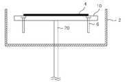
Translated fromKorean도 1은 종래 진공증착 공정에 이용되는 평판표시소자의 제조장치의 단면도.1 is a cross-sectional view of an apparatus for manufacturing a flat panel display device used in a conventional vacuum deposition process.
도 2a는 진공증착 공정 후 발생 되는 정전기에 의해 기판이 휘어지는 것을 도시한 단면도.Figure 2a is a cross-sectional view showing that the substrate is bent by the static electricity generated after the vacuum deposition process.
도 2b는 종래 육안을 통해 정전기량을 검출하는 것을 도시한 단면도.Figure 2b is a cross-sectional view showing the detection of the amount of static electricity through the conventional naked eye.
도 3은 본 발명의 제1 실시예에 따른 진공증착 공정에 이용되는 평판표시소자의 제조장치의 단면도.3 is a cross-sectional view of an apparatus for manufacturing a flat panel display device used in a vacuum deposition process according to a first embodiment of the present invention.
도 4는 본 발명의 제1 실시예에 따른 정전기량 검출장치의 블럭 구성도.4 is a block diagram of the static electricity amount detecting device according to the first embodiment of the present invention.
도 5는 본 발명의 제1 실시예에 따른 정전기량 검출방법의 흐름도.5 is a flowchart of a static electricity amount detecting method according to the first embodiment of the present invention.
도 6은 본 발명의 제2 실시예에 따른 진공증착 공정에 이용되는 평판표시소자의 제조장치의 단면도.6 is a cross-sectional view of a manufacturing apparatus of a flat panel display device used in a vacuum deposition process according to a second embodiment of the present invention.
본 발명은 평판표시소자의 제조장치에 관한 것으로, 특히 진공증착 공정시 발생되는 정전기량을 정확하게 검출할 수 있는 정전기량 검출장치 및 검출방법에 관한 것이다.BACKGROUND OF THE INVENTION 1. Field of the Invention The present invention relates to an apparatus for manufacturing a flat panel display element, and more particularly, to an electrostatic amount detecting device and a detection method capable of accurately detecting an amount of static electricity generated during a vacuum deposition process.
최근의 정보화 사회에서 표시소자는 시각정보 전달매체로서 그 중요성이 어느 때보다 강조되고 있다. 현재 주류를 이루고 있는 음극선관(Cathode Ray Tube) 또는 브라운관은 무게와 부피가 큰 문제점이 있다.In today's information society, display elements are more important than ever as visual information transfer media. Cathode Ray Tube (CRT) or cathode ray tube, which is currently mainstream, has a problem in weight and volume.
평판표시소자에는 액정표시소자(Liquid Crystal Display : LCD), 전계 방출 표시소자(Field Emission Display : FED), 유기 발광다이오드 표시소자( Orgarnic Light Emitting Diode Display : OLED) 등이 있고 이들 대부분이 실용화되어 시판되고 있다.The flat panel display device includes a liquid crystal display (LCD), a field emission display (FED), and an organic light emitting diode display (OLED), and most of them are commercially available. It is becoming.
이 중 액정표시소자는 전자제품의 경박단소 추세를 만족할 수 있고, 양산성이 향상되고 있어 많은 응용분야에서 음극선관을 빠른 속도로 대체하고 있다.Among these, liquid crystal display devices can satisfy the light and thin trend of electronic products, and mass production is improving, and thus, cathode ray tubes are rapidly replaced in many applications.
통상, 액정표시소자(Liquid Crystal Display : " LCD" 라 함)에서는 액정패널 상에 매트릭스 형태로 배열된 액정셀들의 광투과율을 공급되는 비디오 데이타 신호를 조절함으로써 데이타 신호에 해당하는 화상을 패널 상에 표시하게 된다.In general, a liquid crystal display ("LCD") controls a video data signal supplied with light transmittance of liquid crystal cells arranged in a matrix form on a liquid crystal panel to display an image corresponding to the data signal on the panel. Will be displayed.
이러한 액정표시소자는 액정층에 전계를 인가하기 위한 전극들, 액정셀 별로 데이타 공급을 절환하기 위한 박막트랜지스터, 외부에서 공급되는 데이타를 액정셀들에 공급하는 신호배선 및 박막트랜지스터의 제어신호를 공급하기 위한 신호배선 등이 형성된 하판과, 칼라필터등이 형성된 상판과, 상판과 하판 사이에 형성되어 일정한 셀갭을 확보하는 스페이서와, 스페이서에 의해 상하판 사이에 마련된 공간에 채워진 액정으로 구성된다.The liquid crystal display device includes electrodes for applying an electric field to the liquid crystal layer, a thin film transistor for switching data supply for each liquid crystal cell, a signal line for supplying externally supplied data to the liquid crystal cells, and a control signal for the thin film transistor. A lower plate on which signal wirings and the like are formed, an upper plate on which color filters and the like are formed, a spacer formed between the upper plate and the lower plate to secure a constant cell gap, and a liquid crystal filled in a space provided between the upper and lower plates by the spacer.
이러한 액정표시소자를 포함하는 평판표시소자의 제조방법에 있어서, 박막트랜지스터의 채널부로 포함되는 활성층과 박막트랜지스터를 보호하는 보호막은 통상 PECVD(Plasma Enhanced Chemical Vapor Deposition) 공정을 이용하여 형성되게 된다. 이러한 PECVD공정은 도 1에 도시된 바와 같은 평판표시소자의 제조장치에 의해 수행되게 된다.In the method of manufacturing a flat panel display device including the liquid crystal display device, the active layer included in the channel portion of the thin film transistor and the protective film for protecting the thin film transistor are usually formed using a PECVD (Plasma Enhanced Chemical Vapor Deposition) process. This PECVD process is performed by the apparatus for manufacturing a flat panel display device as shown in FIG.
도 1에 도시된 평판표시소자의 제조장치는 증착공정이 수행되는 프로세서 챔버(2)와, 프로세서 챔버(2) 내에서 기판(4)을 가열함과 아울러 플라즈마를 발생시키기 위한 하부전극으로 이용되는 서셉터(10)를 구비한다. 서셉터(10) 상에는 기판(4)을 지지하기 위한 리프트 핀(6: Lift Pin)이 설치된다. 기판(4)은 로보트 암(미도시)에 의해 서셉터(10) 상으로 이송되거나 증착공정 후 반송되어 진다. 서셉터(10)는 지지대(20)에 고정되고, 이에 의해 프로세서 챔버(2) 내에서 소정의 높이에 위치하게 된다. 이러한 서셉터(10)는 지지대(20)에 연결된 타임벨트(미도시: Time Belt)에 의해 수직방향으로 이동되게 된다.The apparatus for manufacturing a flat panel display device shown in FIG. 1 is used as a lower electrode for generating a plasma while heating a
타임벨트는 모터(미도시)에 의해 구동되어 지지대(20)를 원하는 높이로 이동시킴으로써 서셉터(10)가 프로세스별 해당 포지션으로 이동되게 한다.The time belt is driven by a motor (not shown) to move the
이러한 구성을 가지는 평판표시소자의 제조장치는 기판이 로드된 서셉터(10)를 증착공정을 진행할 수 있는 포지션으로 상승시키고, 기판(4)에 열 및 전압을 인가하여 가스 및 플라즈마에 의해 필요로 하는 막이 유리기판(4) 위에 증착되게 한 다.The apparatus for manufacturing a flat panel display device having such a configuration raises the
그런데, 상기와 같은 증착 공정이 끝나게 되면 RF(Radio Frequency) 방전에 의해 기판과 서셉터(10)사이에 높은 전하가 대전 되며, 이렇게 대전 된 전하(정전기)는 기판과 서셉터를 강하게 부착시키는 원인이 된다.However, when the above deposition process is completed, high charge is charged between the substrate and the
따라서, 도 2a에 도시된 바와 같이, 증착 공정이 종료된 후 서셉터(50) 하강시 리프트 핀(46)이 위치하지 않는 기판의 중앙부는 대전 된 전하에 의해, 기판이 서셉터와 제대로 분리되지 않고 휘어지는 문제가 발생한다.Therefore, as shown in FIG. 2A, the center portion of the substrate where the
이를 방지 하기 위해 일반적으로 증착 공정 완료 후 별도의 제전공정을 거치게 된다. 구체적으로 제전공정은 챔버의 가스 주입구를 통해 He, Ne 과 같은 불활성 가스 또는 N2 가스를 주입하고, 400 W 정도의 RF 파워를 인가하여 주입된 비반응성 가스를 플라즈마 상태로 만든다. 정전기량이 많을수록 RF 파워의 인가시간을 증가시켜야 하며, 이에 의해 더 많이 생성된 비반응성 플라즈마는 기판의 중앙부에 대전 된 전하들을 중화시킨다.In order to prevent this, after the deposition process is completed, a separate static elimination process is generally performed. Specifically, the antistatic process injects an inert gas such as He, Ne or N2 gas through the gas inlet of the chamber, and applies the RF power of about 400 W to make the injected non-reactive gas into a plasma state. The greater the amount of static electricity, the more time the RF power should be applied, and the more non-reactive plasma generated thereby neutralizes the charges charged in the center of the substrate.
그러나, 기판과 접촉되는 서셉터의 상측에 발생 되는 정전기를 제전 처리하여 완전히 제거하기 위해서는 챔버 내의 환경변화 등 여러 요인들로 인해 수시로 변하는 정전기량에 상응하여 RF 파워 인가 시간을 조정하여야 한다.However, in order to completely remove the static electricity generated on the upper side of the susceptor in contact with the substrate, the RF power application time must be adjusted according to the amount of static electricity that changes frequently due to various factors such as environmental changes in the chamber.
이를 위해서는 변화된 정전기량에 대한 정확한 검출이 선행되어야 하는바, 도 2에 도시된 바와 같이 종래에는 챔버(42)의 외부창(70)을 통해 사용자의 육안(80)을 통해 변화된 정전기량을 검출하였다. 즉, 증착 공정이 완료된 후, 서셉터 (50) 하강시 서셉터(50)상에 발생 된 정전기로 인해 기판이 휘어졌다가 서셉터(50)로부터 완전히 분리되는 시점을 육안(80)으로 확인하고, 이때의 서셉터(50) 하강위치에 비례하여 대략적인 정전기량을 검출하였다.To this end, accurate detection of the changed amount of static electricity must be preceded. As shown in FIG. 2, the amount of static electricity changed through the user's naked eye 80 is detected through the
그러나, 이와 같은 종래 정전기량 검출장치 및 방법은 사용자의 육안 확인에만 의존하여 정전기량을 검출함으로 인해, 사용자에게 불편함을 부여하였고 더불어, 발생 된 정확한 정전기량을 판단할 수 없었기에 제전처리 후 잔존하는 정전기에 의해 기판이 파손되는 문제점이 있었다.However, such a conventional static electricity amount detecting device and method has caused inconvenience to the user due to detecting the static electricity amount only by visual confirmation of the user, and since the exact amount of generated static electricity could not be determined, it remains after the static electricity treatment. There was a problem that the substrate is damaged by the static electricity.
따라서, 본 발명의 목적은 수시로 변화되는 정전기량을 정확히 검출할 수 있는 평판표시소자의 제조장치 및 그의 정전기량 검출장치 및 검출방법을 제공하는 데 있다.Accordingly, it is an object of the present invention to provide an apparatus for manufacturing a flat panel display device capable of accurately detecting the amount of static electricity that changes frequently, an apparatus for detecting the amount of static electricity, and a method for detecting the same.
더불어, 본 발명의 또 다른 목적은 제전처리 후 잔존하는 정전기에 의해 기판이 파손되는 것을 방지할 수 있는 평판표시소자의 제조장치 및 그의 정전기량 검출장치 및 검출방법을 제공하는 데 있다.In addition, another object of the present invention is to provide an apparatus for manufacturing a flat panel display device, an electrostatic amount detecting device thereof, and a detecting method capable of preventing a substrate from being damaged by static electricity remaining after the static elimination treatment.
상기 목적을 달성하기 위하여, 본 발명의 제1 실시예에 따른 평판표시소자의 제조장치는 기판을 지지하기 위한 다수의 리프트 핀과; 상기 리프트 핀이 관통되고 승강 가능하게 구동되는 서셉터와; 정전기에 의해 상기 서셉터와 상기 기판이 부착 된 후, 상기 서셉터의 하강으로 인해 상기 서셉터와 상기 기판이 분리되는 시점을 감지하고, 그때의 상기 서셉터의 이동거리를 감지하여 상기 서셉터상의 정전기량을 검출하기 위한 정전기량 검출수단을 포함하는 것을 특징으로 한다.In order to achieve the above object, a manufacturing apparatus of a flat panel display device according to a first embodiment of the present invention includes a plurality of lift pins for supporting a substrate; A susceptor through which the lift pins are penetrated and driven to move up and down; After the susceptor and the substrate are attached by static electricity, the susceptor and the substrate is separated by the falling of the susceptor, and the movement distance of the susceptor at that time is sensed so that the susceptor moves on the susceptor. And static electricity amount detecting means for detecting static electricity amount.
상기 정전기량 검출수단은, 상기 서셉터의 하강시에 상기 서셉터와 상기 기판 사이에 형성되는 공간에 광을 투과시키기 위한 발광부와; 상기 투과된 광을 수광하기 위한 수광부와; 상기 서셉터의 이동거리를 센싱하기 위한 이동거리감지부와; 상기 수광부를 통한 검출 광량과 상기 이동거리 감지값을 이용하여 상기 서셉터상의 정전기량을 검출하는 제어부를 포함하는 것을 특징으로 한다.The static electricity amount detecting means includes: a light emitting part for transmitting light to a space formed between the susceptor and the substrate when the susceptor is lowered; A light receiving unit for receiving the transmitted light; A movement distance sensing unit for sensing a movement distance of the susceptor; And a controller configured to detect the amount of static electricity on the susceptor by using the amount of light detected by the light receiver and the movement distance detection value.
상기 제어부는, 상기 검출 광량이 소정의 기준 광량값 이상이 되면 그때의 상기 이동거리 감지값을 저장하고, 상기 저장된 이동거리 감지값에 따른 정전기량을 검출하는 것을 특징으로 한다.The control unit may store the movement distance detection value at that time when the detection light amount is equal to or greater than a predetermined reference light amount value, and detect the static electricity amount according to the stored movement distance detection value.
상기 제어부는, 소정의 룩 업 테이블에 구축된 정전기량 값들 중에 상기 저장된 이동거리 감지값과 링크되는 정전기량 값을 상기 서셉터상의 정전기량으로 검출하는 것을 특징으로 한다.The controller may detect, as the static electricity amount on the susceptor, the static electricity value linked to the stored moving distance sensing value among the static electricity values established in a predetermined lookup table.
상기 제어부를 통해 검출된 정전기량을 표시하기 위한 표시부를 더 구비하는 것을 특징으로 한다.And a display unit for displaying the amount of static electricity detected through the control unit.
또한, 상기 목적을 달성하기 위하여, 본 발명의 제1 실시예에 따른 정전기량 검출장치는 상기 서셉터의 이동시에 상기 서셉터와 상기 기판 사이에 형성되는 공간에 광을 투과시키기 위한 발광부와; 상기 투과된 광을 수광하기 위한 수광부와; 상기 서셉터의 이동거리를 센싱하기 위한 이동거리감지부와; 상기 수광부를 통한 검출 광량과 상기 이동거리 감지값을 이용하여 상기 서셉터상의 정전기량을 검출하는 제어부를 포함하는 것을 특징으로 한다.In addition, in order to achieve the above object, the electrostatic amount detecting device according to the first embodiment of the present invention includes a light emitting unit for transmitting light to the space formed between the susceptor and the substrate when the susceptor moves; A light receiving unit for receiving the transmitted light; A movement distance sensing unit for sensing a movement distance of the susceptor; And a controller configured to detect the amount of static electricity on the susceptor by using the amount of light detected by the light receiver and the movement distance detection value.
또한, 상기 목적을 달성하기 위하여, 본 발명의 제1 실시예에 따른 정전기량 검출방법은 기판을 지지하기 위한 다수의 리프트 핀, 및 상기 리프트 핀이 관통되고 승강 가능하게 구동되는 서셉터를 가지는 증착장비에서 상기 서셉터상의 정전기량을 검출하는 방법에 있어서, 상기 서셉터의 이동시에 상기 서셉터와 상기 기판 사이에 형성되는 공간에 광을 투과시킴과 동시에, 상기 서셉터의 이동시에 상기 서셉터의 이동거리를 센싱하는 제1 단계와; 상기 투과된 광량과 상기 이동거리 감지값을 이용하여 상기 서셉터상의 정전기량을 검출하는 제2 단계를 포함하는 것을 특징으로 한다.In addition, in order to achieve the above object, the electrostatic amount detection method according to the first embodiment of the present invention is a deposition having a plurality of lift pins for supporting a substrate, and a susceptor through which the lift pins are driven and liftable A method of detecting an amount of static electricity on the susceptor in an equipment, the method comprising: transmitting light to a space formed between the susceptor and the substrate when the susceptor is moved, and at the time of movement of the susceptor A first step of sensing a moving distance; And detecting the amount of static electricity on the susceptor by using the transmitted light amount and the movement distance detection value.
상기 제2 단계는, 상기 투과된 광량이 소정의 기준 광량값 이상이 되면 그때의 상기 이동거리 감지값을 저장하는 제2-1 단계와; 소정의 룩 업 테이블에 구축된 정전기량 값들 중에 상기 저장된 이동거리 감지값과 링크되는 정전기량 값을 상기 서셉터상의 정전기량으로 검출하는 제2-2 단계를 포함하는 것을 특징으로 한다.The second step may include: a second step of storing the moving distance detection value at the time when the transmitted light amount is equal to or greater than a predetermined reference light amount value; And a step 2-2 of detecting the amount of static electricity linked to the stored moving distance sensing value as the amount of static electricity on the susceptor among the static electricity values established in the predetermined lookup table.
또한, 상기 목적을 달성하기 위하여, 본 발명의 제2 실시예에 따른 평판표시소자의 제조장치는 기판을 지지하기 위한 다수의 리프트 핀과; 상기 리프트 핀이 관통되고 승강 가능하게 구동되는 서셉터와; 정전기에 의해 상기 서셉터와 상기 기판이 부착된 후, 상기 리프트 핀의 상승으로 인해 상기 서셉터와 상기 기판이 분리되는 시점을 감지하고, 그때의 상기 리프트 핀의 이동거리를 감지하여 상기 서셉터상의 정전기량을 검출하기 위한 정전기량 검출수단을 포함하는 것을 특징으로 한 다.In addition, in order to achieve the above object, a manufacturing apparatus of a flat panel display device according to a second embodiment of the present invention includes a plurality of lift pins for supporting a substrate; A susceptor through which the lift pins are penetrated and driven to move up and down; After the susceptor and the substrate are attached by static electricity, the time when the susceptor and the substrate is separated by the lift pin is sensed, and the moving distance of the lift pin at that time is sensed to It characterized in that it comprises a static electricity amount detecting means for detecting the static electricity amount.
상기 목적 외에 본 발명의 다른 목적 및 특징들은 첨부도면을 참조한 실시 예에 대한 설명을 통하여 명백하게 드러나게 될 것이다.Other objects and features of the present invention in addition to the above object will be apparent from the description of the embodiments with reference to the accompanying drawings.
이하, 도 3 내지 도 6을 참조하여 본 발명의 바람직한 실시 예에 대하여 설명하기로 한다.Hereinafter, exemplary embodiments of the present invention will be described with reference to FIGS. 3 to 6.
도 3은 본 발명의 제1 실시예에 따른 평판표시소자의 제조장치에 대한 단면도이다.3 is a cross-sectional view of an apparatus for manufacturing a flat panel display device according to a first embodiment of the present invention.
도 3을 참조하면, 본 발명의 제1 실시예에 따른 평판표시소자의 제조장치는 증착공정이 수행되는 프로세서 챔버(102)와, 프로세서 챔버(102) 내에서 기판(104)을 지지하기 위한 다수의 리프트 핀(106:Lift Pin)과, 상기 리프트 핀이 관통되고 승강 가능하게 구동되는 서셉터(110)와, 정전기에 의해 상기 서셉터(110)와 기판(104)이 부착된 후, 서셉터(110)의 하강으로 인해 서셉터(110)와 기판(104)이 분리되는 시점을 감지하고, 그때의 서셉터(110)의 이동거리를 감지하여 서셉터(110)상의 정전기량을 검출하기 위한 정전기량 검출수단을 구비한다.Referring to FIG. 3, an apparatus for manufacturing a flat panel display device according to a first exemplary embodiment of the present invention includes a
정전기량 검출수단은 서셉터(110) 하강시 서셉터(110)와 기판(104)이 분리되는 시점을 감지하기 위한 기판(104)과 서셉터(110) 사이에 형성되는 공간을 횡단하여 진행하는 광을 발생시키는 발광센서(116) 및 이를 수광하는 수광센서(118)와, 서셉터(110) 하강시 서셉터(110)의 이동거리를 감지하기 위한 이동거리 감지센서(122)를 구비한다.The amount of static electricity detecting means proceeds across the space formed between the
이러한 구성수단을 가지는 본 발명의 제1 실시예에 따른 평판표시소자의 제 조장치를 이용하여 서셉터상의 정전기량을 검출하는 과정을 살펴보면 다음과 같다.Looking at the process of detecting the amount of static electricity on the susceptor using the manufacturing apparatus of the flat panel display device according to the first embodiment of the present invention having such a configuration as follows.
증착공정이 완료된 기판(104)이 로봇암(미도시)에 의해 후속 공정으로 반송되도록 하기 위해 서셉터(110)는 소정 거리만큼 아래로 하강한다.The
이때, 서셉터(110)는 지지대(120)에 고정되어 있기 때문에 지지대(120)에 연결된 타임벨트(114: Time Belt)와, 타임벨트(114)를 구동하기 위한 모터(112)에 의해 수직방향으로 이동되게 된다.At this time, since the
한편, 증착공정을 위한 RF 방전에 의해 기판(104)과 서셉터(110)사이에 높은 전하가 대전 되어 있으며, 이로 인해 서셉터 하강시 리프트 핀이 위치하지 않는 기판의 중앙부는 정전기에 의해 기판과 서셉터가 제대로 분리되지 않고 그 결과 기판은 휘어진다. 이러한 이유로 대전된 전하를 중화시키기 위한 제전처리가 행해지는데, 완전한 제전을 위해서는 선행적으로 정확한 정전기량이 검출되어야 한다.On the other hand, high charge is charged between the
따라서, 정확한 정전기량의 검출을 위해, 모터(112)에 의해 구동되는 타임벨트(114)의 작동으로 지지대(120)에 고정된 서셉터(110)가 지지대(120)와 함께 하강하는 순간, 서셉터(110)의 일측 근방에 설치되어 있는 발광센서(116)는 광을 발생시켜 기판(104)과 서셉터(110) 사이에 형성되는 공간으로 광을 횡단시킨다. 횡단 된 광은 서셉터(110)의 타측 근방에 설치되어 있는 수광센서(118)에 의해 수광된다. 여기서, 수광센서(118)에 의해 수광된 광량값이 기판(104)과 서셉터(110)가 완전히 분리되는 시점을 판단하기 위해 미리 정해진 기준광량값 이상이 될 때까지, 발광센서(116)는 도시하지 않은 제어부의 제어에 의해 발광한다.Therefore, for accurate detection of the amount of static electricity, the moment the
또한, 정확한 정전기량의 검출을 위해, 모터(112)에 의해 구동되는 타임벨트 (114)의 작동으로 지지대(120)에 고정된 서셉터(110)가 지지대(120)와 함께 하강하는 순간, 서셉터(110)의 하강거리를 감지하기 위한 이동거리 감지센서(122)는 센싱동작을 시작한다. 여기서 이동거리 감지센서(122)는 하나의 모듈내에 집적된 발·수광부로 구성되어, 발광부로부터 발생된 광이 지지대(120)의 일측에 설치된 피감지부(124)로부터 반사되면 수광부를 통해 그 반사광을 수광한다. 그리고, 이동거리 감지센서(122)는 수광된 광을 전기적 신호로 변환하고, 전기적 신호의 전류량에 근거하여 서셉터의 이동거리(하강거리)를 센싱한다.In addition, in order to accurately detect the amount of static electricity, the moment when the
이러한 이동거리 감지센서(122)는 도시하지 않은 제어부의 제어에 의해 서셉터(110)의 하강순간부터 시작하여 일정시점(기판과 서셉터가 완전히 분리되는 시점)까지 계속하여 서셉터의 이동거리를 센싱한다.The
도시하지 않은 제어부는 수광센서에 의해 수광된 빛의 광량이 기준광량값 이상이 될 때의 서셉터(110)의 이동거리를 이용하여 서셉터(110)상의 정전기량을 검출한다. 이에 대해서는 도 4를 통해 상세히 설명하기로 한다.The control unit (not shown) detects the amount of static electricity on the
도 4는 본 발명의 제1 실시예에 따른 정전기량 검출장치에 대한 블럭 구성도이다.4 is a block diagram of the static electricity amount detecting device according to the first embodiment of the present invention.
도 4를 참조하면, 본 발명의 제1 실시예에 따른 정전기량 검출장치는 서셉터의 하강시에 서셉터와 기판 사이에 형성되는 공간에 광을 투과시키기 위한 발광부(216)와, 투과된 광을 수광하기 위한 수광부(218)와, 서셉터의 이동거리를 센싱하기 위한 이동거리감지부(240)와, 수광부(218)를 통한 검출 광량과 이동거리 감지값을 이용하여 서셉터상의 정전기량을 검출하는 제어부(250)와, 검출된 정전기량을 표시하기 위한 표시부(260)를 구비한다.Referring to FIG. 4, the electrostatic amount detecting device according to the first embodiment of the present invention includes a
증착공정을 위한 RF 방전에 의해 기판과 서셉터 사이에 발생되는 정전기량을 검출하기 위해, 제어부(250)는 서셉터 하강과 동시에 발광부(216)에 제어신호를 인가하여 발광부(216)로 하여금 기판과 서셉터 사이에 형성되는 공간으로 광을 투과시키게 한다.In order to detect the amount of static electricity generated between the substrate and the susceptor by the RF discharge for the deposition process, the
또한, 제어부(250)는 서셉터 하강과 동시에 이동거리감지부(240)에 제어신호를 인가하여 서셉터의 이동거리(하강거리)를 실시간으로 감지하게 한다.In addition, the
발광부(216)로부터 발광된 광은 기판과 서셉터 사이에 형성되는 공간을 투과하여 수광부(218)로 수광된다. 수광부(218)에서 수광된 광은 광전변환부(220)를 거쳐 전기적 신호로 변환되어 A/D변환부(222)로 입력된다. A/D변환부(222)를 통해 입력된 아날로그 신호는 디지털 신호로 변환되어 제어부(250)로 입력된다.Light emitted from the
서셉터 하강시 리프트 핀이 위치하지 않는 기판의 중앙부는 정전기로 인해 어느 시점(기판과 서셉터가 완전히 분리되는 시점)까지는 기판과 서셉터가 제대로 분리되지 않고 붙어있는 상태를 유지하므로 그 결과 투과되는 광은 기판에 의해 반사되거나 간섭되어 발광량 대비 수광량은 현저히 저하된다.When the susceptor is lowered, the center part of the board where the lift pin is not located remains at the point where the board and the susceptor are not properly separated and adhered to each other due to the static electricity. Light is reflected or interfered by the substrate so that the amount of light received is significantly lower than the amount of light emitted.
따라서, 제어부(250)는 기판과 서셉터가 완전히 분리되는 시점을 판단하기 위해 미리 설정된 소정의 기준 광량값과 상기 A/D변환부(222)에 의해 입력되는 디지털 신호값을 비교한다. 비교결과, 디지털 신호값이 기준광량값 이상이 되면 제어부(250)는 기판과 서셉터가 완전히 분리되었다고 판단한다.Accordingly, the
이때, 제어부(250)는 이동거리감지부(240)로터 실시간으로 입력받는 서셉터 의 이동거리 감지값들 중에서 상기 디지털 신호값이 기준광량값 이상이 될 때의 이동거리 감지값을 저장한다. 저장된 이동거리 감지값은 서셉터의 이동거리에 상응되게 메모리부(미도시)의 룩업 테이블에 미리 설정된 정전기량값에 링크되며, 이렇게 링크된 정전기량값이 서셉터상의 정전기량으로 검출된다.At this time, the
상기 검출된 정전기량은 표시부(260)를 통해 사용자에게 현시될 수 있으며, 사용자는 이를 기초로 하여 RF 파워(통상 400W) 인가시간을 조정함으로써, 서셉터상의 정전기를 제거할 수 있다.The detected amount of static electricity may be displayed to the user through the
도 5는 본 발명의 제1 실시예에 따른 정전기량 검출방법의 흐름도이다.5 is a flowchart of a static electricity amount detecting method according to the first embodiment of the present invention.
도 5를 참조하면, 먼저 서셉터는 증착공정이 완료된 기판이 후속공정으로 이송되도록 로봇암의 진입공간을 마련하기 위해 소정거리만큼 하강한다. (S310)Referring to FIG. 5, the susceptor is first lowered by a predetermined distance to prepare an entry space of the robot arm so that the substrate on which the deposition process is completed is transferred to the subsequent process. (S310)
그런데, 증착공정을 위한 RF 방전에 의해 기판과 서셉터 사이에는 소정의 정전기가 발생되고, 이로 인해 서셉터 하강시 리프트 핀이 위치하지 않는 기판의 중앙부는 정전기로 인해 어느 시점(기판과 서셉터가 완전히 분리되는 시점)까지는 기판과 서셉터가 제대로 분리되지 않고 붙어있는 상태를 유지한다. (S320)However, a predetermined static electricity is generated between the substrate and the susceptor by the RF discharge for the deposition process. As a result, the center portion of the substrate where the lift pin is not located when the susceptor descends is discharged at some point due to the static electricity. The substrate and susceptor are not separated properly but remain attached. (S320)
따라서, 발생되는 정전기량을 검출하기 위해, 제어부의 제어신호에 의해 서셉터 하강과 동시에 발광부는 기판과 서셉터 사이에 형성되는 공간으로 광을 투과시킨다.Therefore, in order to detect the amount of static electricity generated, the light emitter transmits light to a space formed between the substrate and the susceptor at the same time as the susceptor is lowered by the control signal of the controller.
또한, 제어부의 제어신호에 의해 서셉터 하강과 동시에 이동거리감지부는 서셉터의 이동거리(하강거리)를 실시간으로 감지한다. (S330)In addition, the movement distance detection unit detects the movement distance (falling distance) of the susceptor in real time at the same time as the susceptor falls by the control signal of the controller. (S330)
발광부로부터 발광 된 광은 기판과 서셉터 사이에 형성되는 공간을 투과하여 수광부로 수광된다. 수광부에서 수광된 광은 광전변환부를 거쳐 전기적 신호로 변환되고 다시 A/D변환부를 거침으로써 디지털 신호로 변환되어 제어부로 입력된다. 이때 이동거리감지부에 의해 감지된 서셉터의 이동거리도 실시간으로 제어부로 입력된다. (S340)The light emitted from the light emitting part is received by the light receiving part through the space formed between the substrate and the susceptor. The light received by the light receiving unit is converted into an electrical signal through the photoelectric conversion unit and then converted into a digital signal through the A / D conversion unit and input to the controller. At this time, the movement distance of the susceptor detected by the movement distance detection unit is also input to the controller in real time. (S340)
제어부는 기판과 서셉터가 완전히 분리되는 시점을 판단하기 위해 미리 설정된 소정의 기준 광량값과 A/D변환부를 거친 디지털 신호값을 비교한다. 비교결과, 디지털 신호값이 기준광량값에 미달 되면 제어부는 기판과 서셉터가 완전히 분리되지 않았다고 판단하여 디지털 신호값이 기준광량값에 도달될 때까지 계속해서 상기 디지털 신호값과 감지된 이동거리값을 입력받는다. (S350)The controller compares a predetermined reference light quantity value preset with a digital signal value passed through the A / D converter to determine when the substrate and the susceptor are completely separated. As a result of the comparison, if the digital signal value is lower than the reference light intensity value, the controller determines that the substrate and the susceptor are not completely separated, and the digital signal value and the detected moving distance value are continued until the digital signal value reaches the reference light intensity value. Get input. (S350)
비교결과, 디지털 신호값이 기준광량값 이상이 되면 제어부는 기판과 서셉터가 완전히 분리되었다고 판단하고, 이때의 서셉터의 이동거리 감지값을 저장한다. (S360)As a result of the comparison, when the digital signal value is equal to or greater than the reference light quantity value, the controller determines that the substrate and the susceptor are completely separated, and stores the movement distance detection value of the susceptor at this time. (S360)
저장된 이동거리 감지값은 서셉터의 이동거리에 상응되게 메모리부(미도시)의 룩업 테이블에 미리 설정된 정전기량값에 링크되며, 이렇게 링크된 정전기량값이 서셉터상의 정전기량으로 검출된다. (S370)The stored movement distance detection value is linked to a static electricity value preset in a look-up table of a memory unit (not shown) corresponding to the movement distance of the susceptor, and the linked static electricity value is detected as the static electricity amount on the susceptor. (S370)
검출된 정전기량은 표시부를 통해 사용자에게 현시된다. (S380)The amount of static electricity detected is manifested to the user through the display. (S380)
도 5는 본 발명의 제2 실시예에 따른 평판표시소자의 제조장치에 대한 단면도이다.5 is a cross-sectional view of an apparatus for manufacturing a flat panel display device according to a second exemplary embodiment of the present invention.
도 5를 참조하면, 본 발명의 제2 실시예에 따른 평판표시소자의 제조장치는 증착공정이 수행되는 프로세서 챔버(302)와, 프로세서 챔버(302) 내에서 기판(304) 을 지지하기 위한 다수의 리프트 핀(306:Lift Pin)과, 상기 리프트 핀이 관통되고 승강 가능하게 구동되는 서셉터(310)와, 정전기에 의해 상기 서셉터(310)와 기판(304)이 부착된 후, 리프트 핀(306)의 상승으로 인해 서셉터(310)와 기판(304)이 분리되는 시점을 감지하고, 그때의 리프트 핀(306)의 이동거리를 감지하여 서셉터(310)상의 정전기량을 검출하기 위한 정전기량 검출수단을 구비한다.Referring to FIG. 5, an apparatus for manufacturing a flat panel display device according to a second exemplary embodiment includes a
정전기량 검출수단은 리프트 핀(306) 상승시 서셉터(310)와 기판(304)이 분리되는 시점을 감지하기 위해 기판(304)과 서셉터(310) 사이에 형성되는 공간을 횡단하여 진행하는 광을 발생시키는 발광센서(316) 및 이를 수광하는 수광센서(318)와, 리프트 핀(306) 상승시 서셉터(310)의 이동거리를 감지하기 위한 이동거리 감지센서(322)를 구비한다.The electrostatic amount detecting means travels across the space formed between the
이러한 구성수단을 가지는 본 발명의 제2 실시예에 따른 평판표시소자의 제조장치를 이용하여 서셉터상의 정전기량을 검출하는 과정을 살펴보면 다음과 같다.Looking at the process of detecting the amount of static electricity on the susceptor using the apparatus for manufacturing a flat panel display device according to a second embodiment of the present invention having such a configuration as follows.
증착공정이 완료된 기판(304)이 로봇암(미도시)에 의해 후속 공정으로 반송되도록 하기 위해 리프트 핀(306)은 모터(312)에 의해 소정 거리만큼 위로 상승한다.The lift pins 306 are lifted up by a distance by the
이때, 서셉터(310)는 지지대(320)에 고정되어 있으므로 로봇암이 진입할 수 있는 공간이 마련되게 된다.At this time, since the
한편, 증착공정을 위한 RF 방전에 의해 기판(304)과 서셉터(310)사이에 높은 전하가 대전 되어 있으며, 이로 인해 리프트 핀(306) 상승시 리프트 핀(306)이 위치하지 않는 기판의 중앙부는 정전기에 의해 기판(304)과 서셉터(310)가 제대로 분 리되지 않고 그 결과 기판(304)은 휘어진다. 이러한 이유로 대전된 전하를 중화시키기 위한 제전처리가 행해지는데, 완전한 제전을 위해서는 선행적으로 정확한 정전기량이 검출되어야 한다.On the other hand, high charge is charged between the
따라서, 정확한 정전기량의 검출을 위해, 모터(312)에 의해 리프트 핀(306)이 상승하는 순간, 서셉터(310)의 일측 근방에 설치되어 있는 발광센서(316)는 광을 발생시켜 기판(304)과 서셉터(310) 사이에 형성되는 공간으로 광을 횡단시킨다. 횡단 된 광은 서셉터(310)의 타측 근방에 설치되어 있는 수광센서(318)에 의해 수광된다. 여기서, 수광센서(318)에 의해 수광된 광량값이 기판(304)과 서셉터(310)가 완전히 분리되는 시점을 판단하기 위해 미리 정해진 기준광량값 이상이 될 때까지, 발광센서(316)는 도시하지 않은 제어부의 제어에 의해 발광한다.Therefore, for accurate detection of the amount of static electricity, the moment the
또한, 정확한 정전기량의 검출을 위해, 모터(312)에 의해 리프트 핀(306)이 상승하는 순간, 리프트 핀(306)의 상승거리를 감지하기 위한 이동거리 감지센서(322)는 센싱동작을 시작한다. 여기서 이동거리 감지센서(322)는 하나의 모듈내에 집적된 발·수광부로 구성되어, 발광부로부터 발생된 광이 리프트 핀(306)의 일측에 설치된 피감지부(324)로부터 반사되면 수광부를 통해 그 반사광을 수광한다. 그리고, 이동거리 감지센서(322)는 수광된 광을 전기적 신호로 변환하고, 전기적 신호의 전류량에 근거하여 리프트 핀(306)의 이동거리(상승거리)를 센싱한다.In addition, to accurately detect the amount of static electricity, the moment the
이러한 이동거리 감지센서(322)는 도시하지 않은 제어부의 제어에 의해 리프트 핀(306)의 상승순간부터 시작하여 일정시점(기판과 서셉터가 완전히 분리되는 시점)까지 계속하여 리프트 핀(306)의 이동거리를 센싱한다.The movement
도시하지 않은 제어부는 수광센서(318)에 의해 수광된 빛의 광량이 기준광량값 이상이 될 때의 리프트 핀(306)의 이동거리를 이용하여 서셉터(310)상의 정전기량을 검출한다.The controller (not shown) detects the amount of static electricity on the
이러한 정전기량에 대한 구체적인 검출방법에 대해서는 제1 실시예에서 설명한 바와 같으므로 이하에서는 생략하기로 한다.The specific detection method for the amount of static electricity is as described in the first embodiment and will be omitted below.
한편, 본 발명의 제2 실시예에 따른 평판표시소자의 제조장치도 검출된 정전기량을 표시하기 위해 표시부를 더 구비한다.Meanwhile, the apparatus for manufacturing a flat panel display device according to the second embodiment of the present invention further includes a display unit for displaying the detected amount of static electricity.
상술한 바와 같이, 본 발명에 따른 평판표시소자의 제조장치 및 그의 정전기량 검출장치 및 검출방법은 별도의 광센서를 이용하여 기판과 서셉터의 분리되는 시점을 정확히 판단하고 그때의 서셉터 하강거리(또는 리프트 핀의 상승거리)에 상응되는 정전기량값을 서셉터상의 정전기량으로 검출함으로써, 수시로 변하는 서셉터상의 정전기량을 정확히 검출할 수 있다.As described above, the apparatus for manufacturing a flat panel display device according to the present invention, an apparatus for detecting the amount of static electricity thereof, and a method for detecting the same, accurately determine a time point at which the substrate and the susceptor are separated using a separate optical sensor, and the susceptor falling distance at that time. By detecting the amount of static electricity corresponding to (or the lift distance of the lift pins) the amount of static electricity on the susceptor, it is possible to accurately detect the amount of static electricity on the susceptor that changes frequently.
이에 따라, 제전처리시 RF파워 인가시간을 검출된 정전기량에 맞추어 정확히 조정할 수 있으므로, 간편하면서도 효과적으로 정전기를 제거할 수 있다.Accordingly, since the RF power application time can be accurately adjusted according to the detected amount of static electricity during the antistatic treatment, the static electricity can be easily and effectively removed.
또한, 본 발명에 따른 평판표시소자의 제조장치 및 그의 정전기량 검출장치 및 검출방법은 수시로 변하는 서셉터상의 정전기량을 정확히 검출하여 그에 맞는 제전처리를 함으로써, 잔존하는 정전기에 의해 기판이 파손되는 것을 방지할 수 있다.In addition, the apparatus for manufacturing a flat panel display device according to the present invention, an apparatus for detecting the amount of static electricity, and a method for detecting the same according to the present invention accurately detect an amount of static electricity on a susceptor that changes from time to time and perform an antistatic treatment accordingly, thereby preventing the substrate from being damaged by the remaining static electricity. It can prevent.
이상 설명한 내용을 통해 당업자라면 본 발명의 기술사상을 일탈하지 아니하는 범위에서 다양한 변경 및 수정이 가능함을 알 수 있을 것이다. 따라서, 본 발명의 기술적 범위는 명세서의 상세한 설명에 기재된 내용으로 한정되는 것이 아니라 특허 청구의 범위에 의해 정하여져야만 할 것이다.It will be apparent to those skilled in the art that various modifications and variations can be made in the present invention without departing from the spirit or scope of the invention. Therefore, the technical scope of the present invention should not be limited to the contents described in the detailed description of the specification, but should be defined by the claims.
Claims (16)
Translated fromKoreanPriority Applications (2)
| Application Number | Priority Date | Filing Date | Title |
|---|---|---|---|
| KR1020050132294AKR101296911B1 (en) | 2005-12-28 | 2005-12-28 | Apparatus For Fabricating Flat Panel Display, Detector Static Electricity Quantity Thereof And Method For Detecting |
| US11/433,560US9170441B2 (en) | 2005-12-28 | 2006-05-15 | Apparatus for fabricating flat panel display, and apparatus and method for detecting quantity of static electricity thereof |
Applications Claiming Priority (1)
| Application Number | Priority Date | Filing Date | Title |
|---|---|---|---|
| KR1020050132294AKR101296911B1 (en) | 2005-12-28 | 2005-12-28 | Apparatus For Fabricating Flat Panel Display, Detector Static Electricity Quantity Thereof And Method For Detecting |
Publications (2)
| Publication Number | Publication Date |
|---|---|
| KR20070069807A KR20070069807A (en) | 2007-07-03 |
| KR101296911B1true KR101296911B1 (en) | 2013-08-14 |
Family
ID=38193214
Family Applications (1)
| Application Number | Title | Priority Date | Filing Date |
|---|---|---|---|
| KR1020050132294AExpired - Fee RelatedKR101296911B1 (en) | 2005-12-28 | 2005-12-28 | Apparatus For Fabricating Flat Panel Display, Detector Static Electricity Quantity Thereof And Method For Detecting |
Country Status (2)
| Country | Link |
|---|---|
| US (1) | US9170441B2 (en) |
| KR (1) | KR101296911B1 (en) |
Cited By (1)
| Publication number | Priority date | Publication date | Assignee | Title |
|---|---|---|---|---|
| US12235287B2 (en) | 2021-11-29 | 2025-02-25 | Samsung Electronics Co., Ltd. | Substrate processing apparatus |
Families Citing this family (404)
| Publication number | Priority date | Publication date | Assignee | Title |
|---|---|---|---|---|
| KR101296911B1 (en)* | 2005-12-28 | 2013-08-14 | 엘지디스플레이 주식회사 | Apparatus For Fabricating Flat Panel Display, Detector Static Electricity Quantity Thereof And Method For Detecting |
| US8986456B2 (en) | 2006-10-10 | 2015-03-24 | Asm America, Inc. | Precursor delivery system |
| US10378106B2 (en) | 2008-11-14 | 2019-08-13 | Asm Ip Holding B.V. | Method of forming insulation film by modified PEALD |
| US9394608B2 (en) | 2009-04-06 | 2016-07-19 | Asm America, Inc. | Semiconductor processing reactor and components thereof |
| US8877655B2 (en) | 2010-05-07 | 2014-11-04 | Asm America, Inc. | Systems and methods for thin-film deposition of metal oxides using excited nitrogen-oxygen species |
| US8802201B2 (en) | 2009-08-14 | 2014-08-12 | Asm America, Inc. | Systems and methods for thin-film deposition of metal oxides using excited nitrogen-oxygen species |
| US8883270B2 (en) | 2009-08-14 | 2014-11-11 | Asm America, Inc. | Systems and methods for thin-film deposition of metal oxides using excited nitrogen—oxygen species |
| US9312155B2 (en) | 2011-06-06 | 2016-04-12 | Asm Japan K.K. | High-throughput semiconductor-processing apparatus equipped with multiple dual-chamber modules |
| US9793148B2 (en) | 2011-06-22 | 2017-10-17 | Asm Japan K.K. | Method for positioning wafers in multiple wafer transport |
| US10364496B2 (en) | 2011-06-27 | 2019-07-30 | Asm Ip Holding B.V. | Dual section module having shared and unshared mass flow controllers |
| US10854498B2 (en) | 2011-07-15 | 2020-12-01 | Asm Ip Holding B.V. | Wafer-supporting device and method for producing same |
| US20130023129A1 (en) | 2011-07-20 | 2013-01-24 | Asm America, Inc. | Pressure transmitter for a semiconductor processing environment |
| US9096931B2 (en) | 2011-10-27 | 2015-08-04 | Asm America, Inc | Deposition valve assembly and method of heating the same |
| US9341296B2 (en) | 2011-10-27 | 2016-05-17 | Asm America, Inc. | Heater jacket for a fluid line |
| US9017481B1 (en) | 2011-10-28 | 2015-04-28 | Asm America, Inc. | Process feed management for semiconductor substrate processing |
| US9005539B2 (en) | 2011-11-23 | 2015-04-14 | Asm Ip Holding B.V. | Chamber sealing member |
| US9167625B2 (en) | 2011-11-23 | 2015-10-20 | Asm Ip Holding B.V. | Radiation shielding for a substrate holder |
| US9202727B2 (en) | 2012-03-02 | 2015-12-01 | ASM IP Holding | Susceptor heater shim |
| US8946830B2 (en) | 2012-04-04 | 2015-02-03 | Asm Ip Holdings B.V. | Metal oxide protective layer for a semiconductor device |
| TWI622664B (en) | 2012-05-02 | 2018-05-01 | Asm智慧財產控股公司 | Phase stable film, structure and device comprising the same, and method of forming same |
| US8728832B2 (en) | 2012-05-07 | 2014-05-20 | Asm Ip Holdings B.V. | Semiconductor device dielectric interface layer |
| US8933375B2 (en) | 2012-06-27 | 2015-01-13 | Asm Ip Holding B.V. | Susceptor heater and method of heating a substrate |
| US9558931B2 (en) | 2012-07-27 | 2017-01-31 | Asm Ip Holding B.V. | System and method for gas-phase sulfur passivation of a semiconductor surface |
| US9117866B2 (en)* | 2012-07-31 | 2015-08-25 | Asm Ip Holding B.V. | Apparatus and method for calculating a wafer position in a processing chamber under process conditions |
| US9169975B2 (en) | 2012-08-28 | 2015-10-27 | Asm Ip Holding B.V. | Systems and methods for mass flow controller verification |
| US9659799B2 (en) | 2012-08-28 | 2017-05-23 | Asm Ip Holding B.V. | Systems and methods for dynamic semiconductor process scheduling |
| US9021985B2 (en) | 2012-09-12 | 2015-05-05 | Asm Ip Holdings B.V. | Process gas management for an inductively-coupled plasma deposition reactor |
| US9324811B2 (en) | 2012-09-26 | 2016-04-26 | Asm Ip Holding B.V. | Structures and devices including a tensile-stressed silicon arsenic layer and methods of forming same |
| US10714315B2 (en) | 2012-10-12 | 2020-07-14 | Asm Ip Holdings B.V. | Semiconductor reaction chamber showerhead |
| CN102956432B (en)* | 2012-10-19 | 2015-07-22 | 京东方科技集团股份有限公司 | Atmospheric-pressure plasma processing device of display substrate |
| US9640416B2 (en) | 2012-12-26 | 2017-05-02 | Asm Ip Holding B.V. | Single-and dual-chamber module-attachable wafer-handling chamber |
| US8894870B2 (en) | 2013-02-01 | 2014-11-25 | Asm Ip Holding B.V. | Multi-step method and apparatus for etching compounds containing a metal |
| US20160376700A1 (en) | 2013-02-01 | 2016-12-29 | Asm Ip Holding B.V. | System for treatment of deposition reactor |
| US9484191B2 (en) | 2013-03-08 | 2016-11-01 | Asm Ip Holding B.V. | Pulsed remote plasma method and system |
| US9589770B2 (en) | 2013-03-08 | 2017-03-07 | Asm Ip Holding B.V. | Method and systems for in-situ formation of intermediate reactive species |
| US8993054B2 (en) | 2013-07-12 | 2015-03-31 | Asm Ip Holding B.V. | Method and system to reduce outgassing in a reaction chamber |
| US9018111B2 (en) | 2013-07-22 | 2015-04-28 | Asm Ip Holding B.V. | Semiconductor reaction chamber with plasma capabilities |
| US9396934B2 (en) | 2013-08-14 | 2016-07-19 | Asm Ip Holding B.V. | Methods of forming films including germanium tin and structures and devices including the films |
| US9793115B2 (en) | 2013-08-14 | 2017-10-17 | Asm Ip Holding B.V. | Structures and devices including germanium-tin films and methods of forming same |
| US9240412B2 (en) | 2013-09-27 | 2016-01-19 | Asm Ip Holding B.V. | Semiconductor structure and device and methods of forming same using selective epitaxial process |
| US9556516B2 (en) | 2013-10-09 | 2017-01-31 | ASM IP Holding B.V | Method for forming Ti-containing film by PEALD using TDMAT or TDEAT |
| US9605343B2 (en) | 2013-11-13 | 2017-03-28 | Asm Ip Holding B.V. | Method for forming conformal carbon films, structures conformal carbon film, and system of forming same |
| US10179947B2 (en) | 2013-11-26 | 2019-01-15 | Asm Ip Holding B.V. | Method for forming conformal nitrided, oxidized, or carbonized dielectric film by atomic layer deposition |
| US10683571B2 (en) | 2014-02-25 | 2020-06-16 | Asm Ip Holding B.V. | Gas supply manifold and method of supplying gases to chamber using same |
| US10167557B2 (en) | 2014-03-18 | 2019-01-01 | Asm Ip Holding B.V. | Gas distribution system, reactor including the system, and methods of using the same |
| US9447498B2 (en) | 2014-03-18 | 2016-09-20 | Asm Ip Holding B.V. | Method for performing uniform processing in gas system-sharing multiple reaction chambers |
| US11015245B2 (en) | 2014-03-19 | 2021-05-25 | Asm Ip Holding B.V. | Gas-phase reactor and system having exhaust plenum and components thereof |
| US9404587B2 (en) | 2014-04-24 | 2016-08-02 | ASM IP Holding B.V | Lockout tagout for semiconductor vacuum valve |
| US10858737B2 (en) | 2014-07-28 | 2020-12-08 | Asm Ip Holding B.V. | Showerhead assembly and components thereof |
| US9543180B2 (en) | 2014-08-01 | 2017-01-10 | Asm Ip Holding B.V. | Apparatus and method for transporting wafers between wafer carrier and process tool under vacuum |
| US9890456B2 (en) | 2014-08-21 | 2018-02-13 | Asm Ip Holding B.V. | Method and system for in situ formation of gas-phase compounds |
| US9657845B2 (en) | 2014-10-07 | 2017-05-23 | Asm Ip Holding B.V. | Variable conductance gas distribution apparatus and method |
| US10941490B2 (en) | 2014-10-07 | 2021-03-09 | Asm Ip Holding B.V. | Multiple temperature range susceptor, assembly, reactor and system including the susceptor, and methods of using the same |
| KR102300403B1 (en) | 2014-11-19 | 2021-09-09 | 에이에스엠 아이피 홀딩 비.브이. | Method of depositing thin film |
| KR102263121B1 (en) | 2014-12-22 | 2021-06-09 | 에이에스엠 아이피 홀딩 비.브이. | Semiconductor device and manufacuring method thereof |
| US9478415B2 (en) | 2015-02-13 | 2016-10-25 | Asm Ip Holding B.V. | Method for forming film having low resistance and shallow junction depth |
| US10529542B2 (en) | 2015-03-11 | 2020-01-07 | Asm Ip Holdings B.V. | Cross-flow reactor and method |
| US10276355B2 (en) | 2015-03-12 | 2019-04-30 | Asm Ip Holding B.V. | Multi-zone reactor, system including the reactor, and method of using the same |
| US10458018B2 (en) | 2015-06-26 | 2019-10-29 | Asm Ip Holding B.V. | Structures including metal carbide material, devices including the structures, and methods of forming same |
| US10600673B2 (en) | 2015-07-07 | 2020-03-24 | Asm Ip Holding B.V. | Magnetic susceptor to baseplate seal |
| US9899291B2 (en) | 2015-07-13 | 2018-02-20 | Asm Ip Holding B.V. | Method for protecting layer by forming hydrocarbon-based extremely thin film |
| US10043661B2 (en) | 2015-07-13 | 2018-08-07 | Asm Ip Holding B.V. | Method for protecting layer by forming hydrocarbon-based extremely thin film |
| US10083836B2 (en) | 2015-07-24 | 2018-09-25 | Asm Ip Holding B.V. | Formation of boron-doped titanium metal films with high work function |
| US10087525B2 (en) | 2015-08-04 | 2018-10-02 | Asm Ip Holding B.V. | Variable gap hard stop design |
| US9647114B2 (en) | 2015-08-14 | 2017-05-09 | Asm Ip Holding B.V. | Methods of forming highly p-type doped germanium tin films and structures and devices including the films |
| US9711345B2 (en) | 2015-08-25 | 2017-07-18 | Asm Ip Holding B.V. | Method for forming aluminum nitride-based film by PEALD |
| US9960072B2 (en) | 2015-09-29 | 2018-05-01 | Asm Ip Holding B.V. | Variable adjustment for precise matching of multiple chamber cavity housings |
| US9909214B2 (en) | 2015-10-15 | 2018-03-06 | Asm Ip Holding B.V. | Method for depositing dielectric film in trenches by PEALD |
| US10211308B2 (en) | 2015-10-21 | 2019-02-19 | Asm Ip Holding B.V. | NbMC layers |
| US10322384B2 (en) | 2015-11-09 | 2019-06-18 | Asm Ip Holding B.V. | Counter flow mixer for process chamber |
| US9455138B1 (en) | 2015-11-10 | 2016-09-27 | Asm Ip Holding B.V. | Method for forming dielectric film in trenches by PEALD using H-containing gas |
| US9905420B2 (en) | 2015-12-01 | 2018-02-27 | Asm Ip Holding B.V. | Methods of forming silicon germanium tin films and structures and devices including the films |
| US9607837B1 (en) | 2015-12-21 | 2017-03-28 | Asm Ip Holding B.V. | Method for forming silicon oxide cap layer for solid state diffusion process |
| US9735024B2 (en) | 2015-12-28 | 2017-08-15 | Asm Ip Holding B.V. | Method of atomic layer etching using functional group-containing fluorocarbon |
| US9627221B1 (en) | 2015-12-28 | 2017-04-18 | Asm Ip Holding B.V. | Continuous process incorporating atomic layer etching |
| US11139308B2 (en) | 2015-12-29 | 2021-10-05 | Asm Ip Holding B.V. | Atomic layer deposition of III-V compounds to form V-NAND devices |
| US10468251B2 (en) | 2016-02-19 | 2019-11-05 | Asm Ip Holding B.V. | Method for forming spacers using silicon nitride film for spacer-defined multiple patterning |
| US9754779B1 (en) | 2016-02-19 | 2017-09-05 | Asm Ip Holding B.V. | Method for forming silicon nitride film selectively on sidewalls or flat surfaces of trenches |
| US10529554B2 (en) | 2016-02-19 | 2020-01-07 | Asm Ip Holding B.V. | Method for forming silicon nitride film selectively on sidewalls or flat surfaces of trenches |
| US10501866B2 (en) | 2016-03-09 | 2019-12-10 | Asm Ip Holding B.V. | Gas distribution apparatus for improved film uniformity in an epitaxial system |
| US10343920B2 (en) | 2016-03-18 | 2019-07-09 | Asm Ip Holding B.V. | Aligned carbon nanotubes |
| US9892913B2 (en) | 2016-03-24 | 2018-02-13 | Asm Ip Holding B.V. | Radial and thickness control via biased multi-port injection settings |
| US10190213B2 (en) | 2016-04-21 | 2019-01-29 | Asm Ip Holding B.V. | Deposition of metal borides |
| US10865475B2 (en) | 2016-04-21 | 2020-12-15 | Asm Ip Holding B.V. | Deposition of metal borides and silicides |
| US10087522B2 (en) | 2016-04-21 | 2018-10-02 | Asm Ip Holding B.V. | Deposition of metal borides |
| US10032628B2 (en) | 2016-05-02 | 2018-07-24 | Asm Ip Holding B.V. | Source/drain performance through conformal solid state doping |
| US10367080B2 (en) | 2016-05-02 | 2019-07-30 | Asm Ip Holding B.V. | Method of forming a germanium oxynitride film |
| KR102592471B1 (en) | 2016-05-17 | 2023-10-20 | 에이에스엠 아이피 홀딩 비.브이. | Method of forming metal interconnection and method of fabricating semiconductor device using the same |
| US11453943B2 (en) | 2016-05-25 | 2022-09-27 | Asm Ip Holding B.V. | Method for forming carbon-containing silicon/metal oxide or nitride film by ALD using silicon precursor and hydrocarbon precursor |
| US10388509B2 (en) | 2016-06-28 | 2019-08-20 | Asm Ip Holding B.V. | Formation of epitaxial layers via dislocation filtering |
| US10612137B2 (en) | 2016-07-08 | 2020-04-07 | Asm Ip Holdings B.V. | Organic reactants for atomic layer deposition |
| US9859151B1 (en) | 2016-07-08 | 2018-01-02 | Asm Ip Holding B.V. | Selective film deposition method to form air gaps |
| US9793135B1 (en) | 2016-07-14 | 2017-10-17 | ASM IP Holding B.V | Method of cyclic dry etching using etchant film |
| US10714385B2 (en) | 2016-07-19 | 2020-07-14 | Asm Ip Holding B.V. | Selective deposition of tungsten |
| KR102354490B1 (en) | 2016-07-27 | 2022-01-21 | 에이에스엠 아이피 홀딩 비.브이. | Method of processing a substrate |
| KR102532607B1 (en) | 2016-07-28 | 2023-05-15 | 에이에스엠 아이피 홀딩 비.브이. | Substrate processing apparatus and method of operating the same |
| US9887082B1 (en) | 2016-07-28 | 2018-02-06 | Asm Ip Holding B.V. | Method and apparatus for filling a gap |
| US10177025B2 (en) | 2016-07-28 | 2019-01-08 | Asm Ip Holding B.V. | Method and apparatus for filling a gap |
| US9812320B1 (en) | 2016-07-28 | 2017-11-07 | Asm Ip Holding B.V. | Method and apparatus for filling a gap |
| US10395919B2 (en) | 2016-07-28 | 2019-08-27 | Asm Ip Holding B.V. | Method and apparatus for filling a gap |
| US10090316B2 (en) | 2016-09-01 | 2018-10-02 | Asm Ip Holding B.V. | 3D stacked multilayer semiconductor memory using doped select transistor channel |
| US10410943B2 (en) | 2016-10-13 | 2019-09-10 | Asm Ip Holding B.V. | Method for passivating a surface of a semiconductor and related systems |
| US10643826B2 (en) | 2016-10-26 | 2020-05-05 | Asm Ip Holdings B.V. | Methods for thermally calibrating reaction chambers |
| US10435790B2 (en) | 2016-11-01 | 2019-10-08 | Asm Ip Holding B.V. | Method of subatmospheric plasma-enhanced ALD using capacitively coupled electrodes with narrow gap |
| US10229833B2 (en) | 2016-11-01 | 2019-03-12 | Asm Ip Holding B.V. | Methods for forming a transition metal nitride film on a substrate by atomic layer deposition and related semiconductor device structures |
| US10714350B2 (en) | 2016-11-01 | 2020-07-14 | ASM IP Holdings, B.V. | Methods for forming a transition metal niobium nitride film on a substrate by atomic layer deposition and related semiconductor device structures |
| US10643904B2 (en) | 2016-11-01 | 2020-05-05 | Asm Ip Holdings B.V. | Methods for forming a semiconductor device and related semiconductor device structures |
| US10134757B2 (en) | 2016-11-07 | 2018-11-20 | Asm Ip Holding B.V. | Method of processing a substrate and a device manufactured by using the method |
| KR102546317B1 (en) | 2016-11-15 | 2023-06-21 | 에이에스엠 아이피 홀딩 비.브이. | Gas supply unit and substrate processing apparatus including the same |
| US10340135B2 (en) | 2016-11-28 | 2019-07-02 | Asm Ip Holding B.V. | Method of topologically restricted plasma-enhanced cyclic deposition of silicon or metal nitride |
| KR102762543B1 (en) | 2016-12-14 | 2025-02-05 | 에이에스엠 아이피 홀딩 비.브이. | Substrate processing apparatus |
| US11447861B2 (en) | 2016-12-15 | 2022-09-20 | Asm Ip Holding B.V. | Sequential infiltration synthesis apparatus and a method of forming a patterned structure |
| US11581186B2 (en) | 2016-12-15 | 2023-02-14 | Asm Ip Holding B.V. | Sequential infiltration synthesis apparatus |
| US9916980B1 (en) | 2016-12-15 | 2018-03-13 | Asm Ip Holding B.V. | Method of forming a structure on a substrate |
| KR102700194B1 (en) | 2016-12-19 | 2024-08-28 | 에이에스엠 아이피 홀딩 비.브이. | Substrate processing apparatus |
| TWI601962B (en)* | 2016-12-21 | 2017-10-11 | 財團法人工業技術研究院 | Static electricity detecting system and method |
| US10269558B2 (en) | 2016-12-22 | 2019-04-23 | Asm Ip Holding B.V. | Method of forming a structure on a substrate |
| US10867788B2 (en) | 2016-12-28 | 2020-12-15 | Asm Ip Holding B.V. | Method of forming a structure on a substrate |
| US11390950B2 (en) | 2017-01-10 | 2022-07-19 | Asm Ip Holding B.V. | Reactor system and method to reduce residue buildup during a film deposition process |
| US10655221B2 (en) | 2017-02-09 | 2020-05-19 | Asm Ip Holding B.V. | Method for depositing oxide film by thermal ALD and PEALD |
| US10468261B2 (en) | 2017-02-15 | 2019-11-05 | Asm Ip Holding B.V. | Methods for forming a metallic film on a substrate by cyclical deposition and related semiconductor device structures |
| US10529563B2 (en) | 2017-03-29 | 2020-01-07 | Asm Ip Holdings B.V. | Method for forming doped metal oxide films on a substrate by cyclical deposition and related semiconductor device structures |
| US10283353B2 (en) | 2017-03-29 | 2019-05-07 | Asm Ip Holding B.V. | Method of reforming insulating film deposited on substrate with recess pattern |
| US10103040B1 (en) | 2017-03-31 | 2018-10-16 | Asm Ip Holding B.V. | Apparatus and method for manufacturing a semiconductor device |
| USD830981S1 (en) | 2017-04-07 | 2018-10-16 | Asm Ip Holding B.V. | Susceptor for semiconductor substrate processing apparatus |
| KR102457289B1 (en) | 2017-04-25 | 2022-10-21 | 에이에스엠 아이피 홀딩 비.브이. | Method for depositing a thin film and manufacturing a semiconductor device |
| US10446393B2 (en) | 2017-05-08 | 2019-10-15 | Asm Ip Holding B.V. | Methods for forming silicon-containing epitaxial layers and related semiconductor device structures |
| US10770286B2 (en) | 2017-05-08 | 2020-09-08 | Asm Ip Holdings B.V. | Methods for selectively forming a silicon nitride film on a substrate and related semiconductor device structures |
| US10892156B2 (en) | 2017-05-08 | 2021-01-12 | Asm Ip Holding B.V. | Methods for forming a silicon nitride film on a substrate and related semiconductor device structures |
| US10504742B2 (en) | 2017-05-31 | 2019-12-10 | Asm Ip Holding B.V. | Method of atomic layer etching using hydrogen plasma |
| US10886123B2 (en) | 2017-06-02 | 2021-01-05 | Asm Ip Holding B.V. | Methods for forming low temperature semiconductor layers and related semiconductor device structures |
| US12040200B2 (en) | 2017-06-20 | 2024-07-16 | Asm Ip Holding B.V. | Semiconductor processing apparatus and methods for calibrating a semiconductor processing apparatus |
| US11306395B2 (en) | 2017-06-28 | 2022-04-19 | Asm Ip Holding B.V. | Methods for depositing a transition metal nitride film on a substrate by atomic layer deposition and related deposition apparatus |
| US10685834B2 (en) | 2017-07-05 | 2020-06-16 | Asm Ip Holdings B.V. | Methods for forming a silicon germanium tin layer and related semiconductor device structures |
| KR20190009245A (en) | 2017-07-18 | 2019-01-28 | 에이에스엠 아이피 홀딩 비.브이. | Methods for forming a semiconductor device structure and related semiconductor device structures |
| US11374112B2 (en) | 2017-07-19 | 2022-06-28 | Asm Ip Holding B.V. | Method for depositing a group IV semiconductor and related semiconductor device structures |
| US10541333B2 (en) | 2017-07-19 | 2020-01-21 | Asm Ip Holding B.V. | Method for depositing a group IV semiconductor and related semiconductor device structures |
| US11018002B2 (en) | 2017-07-19 | 2021-05-25 | Asm Ip Holding B.V. | Method for selectively depositing a Group IV semiconductor and related semiconductor device structures |
| US10590535B2 (en) | 2017-07-26 | 2020-03-17 | Asm Ip Holdings B.V. | Chemical treatment, deposition and/or infiltration apparatus and method for using the same |
| US10312055B2 (en) | 2017-07-26 | 2019-06-04 | Asm Ip Holding B.V. | Method of depositing film by PEALD using negative bias |
| US10605530B2 (en) | 2017-07-26 | 2020-03-31 | Asm Ip Holding B.V. | Assembly of a liner and a flange for a vertical furnace as well as the liner and the vertical furnace |
| TWI815813B (en) | 2017-08-04 | 2023-09-21 | 荷蘭商Asm智慧財產控股公司 | Showerhead assembly for distributing a gas within a reaction chamber |
| US10692741B2 (en) | 2017-08-08 | 2020-06-23 | Asm Ip Holdings B.V. | Radiation shield |
| US10770336B2 (en) | 2017-08-08 | 2020-09-08 | Asm Ip Holding B.V. | Substrate lift mechanism and reactor including same |
| US11769682B2 (en) | 2017-08-09 | 2023-09-26 | Asm Ip Holding B.V. | Storage apparatus for storing cassettes for substrates and processing apparatus equipped therewith |
| US11139191B2 (en) | 2017-08-09 | 2021-10-05 | Asm Ip Holding B.V. | Storage apparatus for storing cassettes for substrates and processing apparatus equipped therewith |
| US10249524B2 (en) | 2017-08-09 | 2019-04-02 | Asm Ip Holding B.V. | Cassette holder assembly for a substrate cassette and holding member for use in such assembly |
| US10236177B1 (en) | 2017-08-22 | 2019-03-19 | ASM IP Holding B.V.. | Methods for depositing a doped germanium tin semiconductor and related semiconductor device structures |
| USD900036S1 (en) | 2017-08-24 | 2020-10-27 | Asm Ip Holding B.V. | Heater electrical connector and adapter |
| US11830730B2 (en) | 2017-08-29 | 2023-11-28 | Asm Ip Holding B.V. | Layer forming method and apparatus |
| US11295980B2 (en) | 2017-08-30 | 2022-04-05 | Asm Ip Holding B.V. | Methods for depositing a molybdenum metal film over a dielectric surface of a substrate by a cyclical deposition process and related semiconductor device structures |
| US11056344B2 (en) | 2017-08-30 | 2021-07-06 | Asm Ip Holding B.V. | Layer forming method |
| KR102491945B1 (en) | 2017-08-30 | 2023-01-26 | 에이에스엠 아이피 홀딩 비.브이. | Substrate processing apparatus |
| KR102401446B1 (en) | 2017-08-31 | 2022-05-24 | 에이에스엠 아이피 홀딩 비.브이. | Substrate processing apparatus |
| US10607895B2 (en) | 2017-09-18 | 2020-03-31 | Asm Ip Holdings B.V. | Method for forming a semiconductor device structure comprising a gate fill metal |
| KR102630301B1 (en) | 2017-09-21 | 2024-01-29 | 에이에스엠 아이피 홀딩 비.브이. | Method of sequential infiltration synthesis treatment of infiltrateable material and structures and devices formed using same |
| US10844484B2 (en) | 2017-09-22 | 2020-11-24 | Asm Ip Holding B.V. | Apparatus for dispensing a vapor phase reactant to a reaction chamber and related methods |
| US10658205B2 (en) | 2017-09-28 | 2020-05-19 | Asm Ip Holdings B.V. | Chemical dispensing apparatus and methods for dispensing a chemical to a reaction chamber |
| US10403504B2 (en) | 2017-10-05 | 2019-09-03 | Asm Ip Holding B.V. | Method for selectively depositing a metallic film on a substrate |
| US10319588B2 (en) | 2017-10-10 | 2019-06-11 | Asm Ip Holding B.V. | Method for depositing a metal chalcogenide on a substrate by cyclical deposition |
| US10923344B2 (en) | 2017-10-30 | 2021-02-16 | Asm Ip Holding B.V. | Methods for forming a semiconductor structure and related semiconductor structures |
| US10910262B2 (en) | 2017-11-16 | 2021-02-02 | Asm Ip Holding B.V. | Method of selectively depositing a capping layer structure on a semiconductor device structure |
| KR102443047B1 (en) | 2017-11-16 | 2022-09-14 | 에이에스엠 아이피 홀딩 비.브이. | Method of processing a substrate and a device manufactured by the same |
| US11022879B2 (en) | 2017-11-24 | 2021-06-01 | Asm Ip Holding B.V. | Method of forming an enhanced unexposed photoresist layer |
| CN111344522B (en) | 2017-11-27 | 2022-04-12 | 阿斯莫Ip控股公司 | Including clean mini-environment device |
| WO2019103613A1 (en) | 2017-11-27 | 2019-05-31 | Asm Ip Holding B.V. | A storage device for storing wafer cassettes for use with a batch furnace |
| US10290508B1 (en) | 2017-12-05 | 2019-05-14 | Asm Ip Holding B.V. | Method for forming vertical spacers for spacer-defined patterning |
| US10872771B2 (en) | 2018-01-16 | 2020-12-22 | Asm Ip Holding B. V. | Method for depositing a material film on a substrate within a reaction chamber by a cyclical deposition process and related device structures |
| TWI799494B (en) | 2018-01-19 | 2023-04-21 | 荷蘭商Asm 智慧財產控股公司 | Deposition method |
| KR102695659B1 (en) | 2018-01-19 | 2024-08-14 | 에이에스엠 아이피 홀딩 비.브이. | Method for depositing a gap filling layer by plasma assisted deposition |
| USD903477S1 (en) | 2018-01-24 | 2020-12-01 | Asm Ip Holdings B.V. | Metal clamp |
| US11018047B2 (en) | 2018-01-25 | 2021-05-25 | Asm Ip Holding B.V. | Hybrid lift pin |
| USD880437S1 (en) | 2018-02-01 | 2020-04-07 | Asm Ip Holding B.V. | Gas supply plate for semiconductor manufacturing apparatus |
| US10535516B2 (en) | 2018-02-01 | 2020-01-14 | Asm Ip Holdings B.V. | Method for depositing a semiconductor structure on a surface of a substrate and related semiconductor structures |
| US11081345B2 (en) | 2018-02-06 | 2021-08-03 | Asm Ip Holding B.V. | Method of post-deposition treatment for silicon oxide film |
| US10896820B2 (en) | 2018-02-14 | 2021-01-19 | Asm Ip Holding B.V. | Method for depositing a ruthenium-containing film on a substrate by a cyclical deposition process |
| WO2019158960A1 (en) | 2018-02-14 | 2019-08-22 | Asm Ip Holding B.V. | A method for depositing a ruthenium-containing film on a substrate by a cyclical deposition process |
| US10731249B2 (en) | 2018-02-15 | 2020-08-04 | Asm Ip Holding B.V. | Method of forming a transition metal containing film on a substrate by a cyclical deposition process, a method for supplying a transition metal halide compound to a reaction chamber, and related vapor deposition apparatus |
| US10658181B2 (en) | 2018-02-20 | 2020-05-19 | Asm Ip Holding B.V. | Method of spacer-defined direct patterning in semiconductor fabrication |
| KR102636427B1 (en) | 2018-02-20 | 2024-02-13 | 에이에스엠 아이피 홀딩 비.브이. | Substrate processing method and apparatus |
| US10975470B2 (en) | 2018-02-23 | 2021-04-13 | Asm Ip Holding B.V. | Apparatus for detecting or monitoring for a chemical precursor in a high temperature environment |
| US11473195B2 (en) | 2018-03-01 | 2022-10-18 | Asm Ip Holding B.V. | Semiconductor processing apparatus and a method for processing a substrate |
| US11629406B2 (en) | 2018-03-09 | 2023-04-18 | Asm Ip Holding B.V. | Semiconductor processing apparatus comprising one or more pyrometers for measuring a temperature of a substrate during transfer of the substrate |
| US11114283B2 (en) | 2018-03-16 | 2021-09-07 | Asm Ip Holding B.V. | Reactor, system including the reactor, and methods of manufacturing and using same |
| KR102646467B1 (en) | 2018-03-27 | 2024-03-11 | 에이에스엠 아이피 홀딩 비.브이. | Method of forming an electrode on a substrate and a semiconductor device structure including an electrode |
| US10510536B2 (en) | 2018-03-29 | 2019-12-17 | Asm Ip Holding B.V. | Method of depositing a co-doped polysilicon film on a surface of a substrate within a reaction chamber |
| US11230766B2 (en) | 2018-03-29 | 2022-01-25 | Asm Ip Holding B.V. | Substrate processing apparatus and method |
| US11088002B2 (en) | 2018-03-29 | 2021-08-10 | Asm Ip Holding B.V. | Substrate rack and a substrate processing system and method |
| KR102501472B1 (en) | 2018-03-30 | 2023-02-20 | 에이에스엠 아이피 홀딩 비.브이. | Substrate processing method |
| KR102600229B1 (en) | 2018-04-09 | 2023-11-10 | 에이에스엠 아이피 홀딩 비.브이. | Substrate supporting device, substrate processing apparatus including the same and substrate processing method |
| TWI811348B (en) | 2018-05-08 | 2023-08-11 | 荷蘭商Asm 智慧財產控股公司 | Methods for depositing an oxide film on a substrate by a cyclical deposition process and related device structures |
| US12025484B2 (en) | 2018-05-08 | 2024-07-02 | Asm Ip Holding B.V. | Thin film forming method |
| US12272527B2 (en) | 2018-05-09 | 2025-04-08 | Asm Ip Holding B.V. | Apparatus for use with hydrogen radicals and method of using same |
| KR20190129718A (en) | 2018-05-11 | 2019-11-20 | 에이에스엠 아이피 홀딩 비.브이. | Methods for forming a doped metal carbide film on a substrate and related semiconductor device structures |
| KR102596988B1 (en) | 2018-05-28 | 2023-10-31 | 에이에스엠 아이피 홀딩 비.브이. | Method of processing a substrate and a device manufactured by the same |
| US11718913B2 (en) | 2018-06-04 | 2023-08-08 | Asm Ip Holding B.V. | Gas distribution system and reactor system including same |
| TWI840362B (en) | 2018-06-04 | 2024-05-01 | 荷蘭商Asm Ip私人控股有限公司 | Wafer handling chamber with moisture reduction |
| US11286562B2 (en) | 2018-06-08 | 2022-03-29 | Asm Ip Holding B.V. | Gas-phase chemical reactor and method of using same |
| US10797133B2 (en) | 2018-06-21 | 2020-10-06 | Asm Ip Holding B.V. | Method for depositing a phosphorus doped silicon arsenide film and related semiconductor device structures |
| KR102568797B1 (en) | 2018-06-21 | 2023-08-21 | 에이에스엠 아이피 홀딩 비.브이. | Substrate processing system |
| TWI873894B (en) | 2018-06-27 | 2025-02-21 | 荷蘭商Asm Ip私人控股有限公司 | Cyclic deposition methods for forming metal-containing material and films and structures including the metal-containing material |
| KR102854019B1 (en) | 2018-06-27 | 2025-09-02 | 에이에스엠 아이피 홀딩 비.브이. | Periodic deposition method for forming a metal-containing material and films and structures comprising the metal-containing material |
| US10612136B2 (en) | 2018-06-29 | 2020-04-07 | ASM IP Holding, B.V. | Temperature-controlled flange and reactor system including same |
| KR102686758B1 (en) | 2018-06-29 | 2024-07-18 | 에이에스엠 아이피 홀딩 비.브이. | Method for depositing a thin film and manufacturing a semiconductor device |
| US10755922B2 (en) | 2018-07-03 | 2020-08-25 | Asm Ip Holding B.V. | Method for depositing silicon-free carbon-containing film as gap-fill layer by pulse plasma-assisted deposition |
| US10388513B1 (en) | 2018-07-03 | 2019-08-20 | Asm Ip Holding B.V. | Method for depositing silicon-free carbon-containing film as gap-fill layer by pulse plasma-assisted deposition |
| US10767789B2 (en) | 2018-07-16 | 2020-09-08 | Asm Ip Holding B.V. | Diaphragm valves, valve components, and methods for forming valve components |
| US10483099B1 (en) | 2018-07-26 | 2019-11-19 | Asm Ip Holding B.V. | Method for forming thermally stable organosilicon polymer film |
| US11053591B2 (en) | 2018-08-06 | 2021-07-06 | Asm Ip Holding B.V. | Multi-port gas injection system and reactor system including same |
| US10883175B2 (en) | 2018-08-09 | 2021-01-05 | Asm Ip Holding B.V. | Vertical furnace for processing substrates and a liner for use therein |
| US10829852B2 (en) | 2018-08-16 | 2020-11-10 | Asm Ip Holding B.V. | Gas distribution device for a wafer processing apparatus |
| US11430674B2 (en) | 2018-08-22 | 2022-08-30 | Asm Ip Holding B.V. | Sensor array, apparatus for dispensing a vapor phase reactant to a reaction chamber and related methods |
| KR102707956B1 (en) | 2018-09-11 | 2024-09-19 | 에이에스엠 아이피 홀딩 비.브이. | Method for deposition of a thin film |
| US11024523B2 (en) | 2018-09-11 | 2021-06-01 | Asm Ip Holding B.V. | Substrate processing apparatus and method |
| US11049751B2 (en) | 2018-09-14 | 2021-06-29 | Asm Ip Holding B.V. | Cassette supply system to store and handle cassettes and processing apparatus equipped therewith |
| CN110970344B (en) | 2018-10-01 | 2024-10-25 | Asmip控股有限公司 | Substrate holding apparatus, system comprising the same and method of using the same |
| US11232963B2 (en) | 2018-10-03 | 2022-01-25 | Asm Ip Holding B.V. | Substrate processing apparatus and method |
| KR102592699B1 (en) | 2018-10-08 | 2023-10-23 | 에이에스엠 아이피 홀딩 비.브이. | Substrate support unit and apparatuses for depositing thin film and processing the substrate including the same |
| US10847365B2 (en) | 2018-10-11 | 2020-11-24 | Asm Ip Holding B.V. | Method of forming conformal silicon carbide film by cyclic CVD |
| US10811256B2 (en) | 2018-10-16 | 2020-10-20 | Asm Ip Holding B.V. | Method for etching a carbon-containing feature |
| KR102605121B1 (en) | 2018-10-19 | 2023-11-23 | 에이에스엠 아이피 홀딩 비.브이. | Substrate processing apparatus and substrate processing method |
| KR102546322B1 (en) | 2018-10-19 | 2023-06-21 | 에이에스엠 아이피 홀딩 비.브이. | Substrate processing apparatus and substrate processing method |
| USD948463S1 (en) | 2018-10-24 | 2022-04-12 | Asm Ip Holding B.V. | Susceptor for semiconductor substrate supporting apparatus |
| US10381219B1 (en) | 2018-10-25 | 2019-08-13 | Asm Ip Holding B.V. | Methods for forming a silicon nitride film |
| US12378665B2 (en) | 2018-10-26 | 2025-08-05 | Asm Ip Holding B.V. | High temperature coatings for a preclean and etch apparatus and related methods |
| US11087997B2 (en) | 2018-10-31 | 2021-08-10 | Asm Ip Holding B.V. | Substrate processing apparatus for processing substrates |
| KR102748291B1 (en) | 2018-11-02 | 2024-12-31 | 에이에스엠 아이피 홀딩 비.브이. | Substrate support unit and substrate processing apparatus including the same |
| US11572620B2 (en) | 2018-11-06 | 2023-02-07 | Asm Ip Holding B.V. | Methods for selectively depositing an amorphous silicon film on a substrate |
| US11031242B2 (en) | 2018-11-07 | 2021-06-08 | Asm Ip Holding B.V. | Methods for depositing a boron doped silicon germanium film |
| US10818758B2 (en) | 2018-11-16 | 2020-10-27 | Asm Ip Holding B.V. | Methods for forming a metal silicate film on a substrate in a reaction chamber and related semiconductor device structures |
| US10847366B2 (en) | 2018-11-16 | 2020-11-24 | Asm Ip Holding B.V. | Methods for depositing a transition metal chalcogenide film on a substrate by a cyclical deposition process |
| US10559458B1 (en) | 2018-11-26 | 2020-02-11 | Asm Ip Holding B.V. | Method of forming oxynitride film |
| US12040199B2 (en) | 2018-11-28 | 2024-07-16 | Asm Ip Holding B.V. | Substrate processing apparatus for processing substrates |
| US11217444B2 (en) | 2018-11-30 | 2022-01-04 | Asm Ip Holding B.V. | Method for forming an ultraviolet radiation responsive metal oxide-containing film |
| KR102636428B1 (en) | 2018-12-04 | 2024-02-13 | 에이에스엠 아이피 홀딩 비.브이. | A method for cleaning a substrate processing apparatus |
| US11158513B2 (en) | 2018-12-13 | 2021-10-26 | Asm Ip Holding B.V. | Methods for forming a rhenium-containing film on a substrate by a cyclical deposition process and related semiconductor device structures |
| TWI874340B (en) | 2018-12-14 | 2025-03-01 | 荷蘭商Asm Ip私人控股有限公司 | Method of forming device structure, structure formed by the method and system for performing the method |
| TWI866480B (en) | 2019-01-17 | 2024-12-11 | 荷蘭商Asm Ip 私人控股有限公司 | Methods of forming a transition metal containing film on a substrate by a cyclical deposition process |
| KR102727227B1 (en) | 2019-01-22 | 2024-11-07 | 에이에스엠 아이피 홀딩 비.브이. | Semiconductor processing device |
| CN111524788B (en) | 2019-02-01 | 2023-11-24 | Asm Ip私人控股有限公司 | Method for forming topologically selective films of silicon oxide |
| KR102626263B1 (en) | 2019-02-20 | 2024-01-16 | 에이에스엠 아이피 홀딩 비.브이. | Cyclical deposition method including treatment step and apparatus for same |
| TWI873122B (en) | 2019-02-20 | 2025-02-21 | 荷蘭商Asm Ip私人控股有限公司 | Method of filling a recess formed within a surface of a substrate, semiconductor structure formed according to the method, and semiconductor processing apparatus |
| TWI845607B (en) | 2019-02-20 | 2024-06-21 | 荷蘭商Asm Ip私人控股有限公司 | Cyclical deposition method and apparatus for filling a recess formed within a substrate surface |
| TWI838458B (en) | 2019-02-20 | 2024-04-11 | 荷蘭商Asm Ip私人控股有限公司 | Apparatus and methods for plug fill deposition in 3-d nand applications |
| TWI842826B (en) | 2019-02-22 | 2024-05-21 | 荷蘭商Asm Ip私人控股有限公司 | Substrate processing apparatus and method for processing substrate |
| KR102858005B1 (en) | 2019-03-08 | 2025-09-09 | 에이에스엠 아이피 홀딩 비.브이. | Method for Selective Deposition of Silicon Nitride Layer and Structure Including Selectively-Deposited Silicon Nitride Layer |
| KR102782593B1 (en) | 2019-03-08 | 2025-03-14 | 에이에스엠 아이피 홀딩 비.브이. | Structure Including SiOC Layer and Method of Forming Same |
| US11742198B2 (en) | 2019-03-08 | 2023-08-29 | Asm Ip Holding B.V. | Structure including SiOCN layer and method of forming same |
| JP2020167398A (en) | 2019-03-28 | 2020-10-08 | エーエスエム・アイピー・ホールディング・ベー・フェー | Door openers and substrate processing equipment provided with door openers |
| KR102809999B1 (en) | 2019-04-01 | 2025-05-19 | 에이에스엠 아이피 홀딩 비.브이. | Method of manufacturing semiconductor device |
| KR20200123380A (en) | 2019-04-19 | 2020-10-29 | 에이에스엠 아이피 홀딩 비.브이. | Layer forming method and apparatus |
| KR20200125453A (en) | 2019-04-24 | 2020-11-04 | 에이에스엠 아이피 홀딩 비.브이. | Gas-phase reactor system and method of using same |
| KR20200130121A (en) | 2019-05-07 | 2020-11-18 | 에이에스엠 아이피 홀딩 비.브이. | Chemical source vessel with dip tube |
| US11289326B2 (en) | 2019-05-07 | 2022-03-29 | Asm Ip Holding B.V. | Method for reforming amorphous carbon polymer film |
| KR20200130652A (en) | 2019-05-10 | 2020-11-19 | 에이에스엠 아이피 홀딩 비.브이. | Method of depositing material onto a surface and structure formed according to the method |
| JP7598201B2 (en) | 2019-05-16 | 2024-12-11 | エーエスエム・アイピー・ホールディング・ベー・フェー | Wafer boat handling apparatus, vertical batch furnace and method |
| JP7612342B2 (en) | 2019-05-16 | 2025-01-14 | エーエスエム・アイピー・ホールディング・ベー・フェー | Wafer boat handling apparatus, vertical batch furnace and method |
| USD975665S1 (en) | 2019-05-17 | 2023-01-17 | Asm Ip Holding B.V. | Susceptor shaft |
| USD947913S1 (en) | 2019-05-17 | 2022-04-05 | Asm Ip Holding B.V. | Susceptor shaft |
| USD935572S1 (en) | 2019-05-24 | 2021-11-09 | Asm Ip Holding B.V. | Gas channel plate |
| USD922229S1 (en) | 2019-06-05 | 2021-06-15 | Asm Ip Holding B.V. | Device for controlling a temperature of a gas supply unit |
| KR20200141002A (en) | 2019-06-06 | 2020-12-17 | 에이에스엠 아이피 홀딩 비.브이. | Method of using a gas-phase reactor system including analyzing exhausted gas |
| KR20200141931A (en) | 2019-06-10 | 2020-12-21 | 에이에스엠 아이피 홀딩 비.브이. | Method for cleaning quartz epitaxial chambers |
| KR20200143254A (en) | 2019-06-11 | 2020-12-23 | 에이에스엠 아이피 홀딩 비.브이. | Method of forming an electronic structure using an reforming gas, system for performing the method, and structure formed using the method |
| USD944946S1 (en) | 2019-06-14 | 2022-03-01 | Asm Ip Holding B.V. | Shower plate |
| USD931978S1 (en) | 2019-06-27 | 2021-09-28 | Asm Ip Holding B.V. | Showerhead vacuum transport |
| KR20210005515A (en) | 2019-07-03 | 2021-01-14 | 에이에스엠 아이피 홀딩 비.브이. | Temperature control assembly for substrate processing apparatus and method of using same |
| JP7499079B2 (en) | 2019-07-09 | 2024-06-13 | エーエスエム・アイピー・ホールディング・ベー・フェー | Plasma device using coaxial waveguide and substrate processing method |
| CN112216646A (en) | 2019-07-10 | 2021-01-12 | Asm Ip私人控股有限公司 | Substrate supporting assembly and substrate processing device comprising same |
| KR20210010307A (en) | 2019-07-16 | 2021-01-27 | 에이에스엠 아이피 홀딩 비.브이. | Substrate processing apparatus |
| KR20210010816A (en) | 2019-07-17 | 2021-01-28 | 에이에스엠 아이피 홀딩 비.브이. | Radical assist ignition plasma system and method |
| KR102860110B1 (en) | 2019-07-17 | 2025-09-16 | 에이에스엠 아이피 홀딩 비.브이. | Methods of forming silicon germanium structures |
| US11643724B2 (en) | 2019-07-18 | 2023-05-09 | Asm Ip Holding B.V. | Method of forming structures using a neutral beam |
| TWI839544B (en) | 2019-07-19 | 2024-04-21 | 荷蘭商Asm Ip私人控股有限公司 | Method of forming topology-controlled amorphous carbon polymer film |
| KR20210010817A (en) | 2019-07-19 | 2021-01-28 | 에이에스엠 아이피 홀딩 비.브이. | Method of Forming Topology-Controlled Amorphous Carbon Polymer Film |
| TWI851767B (en) | 2019-07-29 | 2024-08-11 | 荷蘭商Asm Ip私人控股有限公司 | Methods for selective deposition utilizing n-type dopants and/or alternative dopants to achieve high dopant incorporation |
| CN112309900A (en) | 2019-07-30 | 2021-02-02 | Asm Ip私人控股有限公司 | Substrate processing apparatus |
| US12169361B2 (en) | 2019-07-30 | 2024-12-17 | Asm Ip Holding B.V. | Substrate processing apparatus and method |
| CN112309899A (en) | 2019-07-30 | 2021-02-02 | Asm Ip私人控股有限公司 | Substrate processing apparatus |
| US11587815B2 (en) | 2019-07-31 | 2023-02-21 | Asm Ip Holding B.V. | Vertical batch furnace assembly |
| US11227782B2 (en) | 2019-07-31 | 2022-01-18 | Asm Ip Holding B.V. | Vertical batch furnace assembly |
| US11587814B2 (en) | 2019-07-31 | 2023-02-21 | Asm Ip Holding B.V. | Vertical batch furnace assembly |
| CN112323048B (en) | 2019-08-05 | 2024-02-09 | Asm Ip私人控股有限公司 | Liquid level sensor for chemical source container |
| CN112342526A (en) | 2019-08-09 | 2021-02-09 | Asm Ip私人控股有限公司 | Heater assembly including cooling device and method of using same |
| USD965044S1 (en) | 2019-08-19 | 2022-09-27 | Asm Ip Holding B.V. | Susceptor shaft |
| USD965524S1 (en) | 2019-08-19 | 2022-10-04 | Asm Ip Holding B.V. | Susceptor support |
| JP2021031769A (en) | 2019-08-21 | 2021-03-01 | エーエスエム アイピー ホールディング ビー.ブイ. | Production apparatus of mixed gas of film deposition raw material and film deposition apparatus |
| KR20210024423A (en) | 2019-08-22 | 2021-03-05 | 에이에스엠 아이피 홀딩 비.브이. | Method for forming a structure with a hole |
| USD949319S1 (en) | 2019-08-22 | 2022-04-19 | Asm Ip Holding B.V. | Exhaust duct |
| USD940837S1 (en) | 2019-08-22 | 2022-01-11 | Asm Ip Holding B.V. | Electrode |
| USD979506S1 (en) | 2019-08-22 | 2023-02-28 | Asm Ip Holding B.V. | Insulator |
| USD930782S1 (en) | 2019-08-22 | 2021-09-14 | Asm Ip Holding B.V. | Gas distributor |
| KR20210024420A (en) | 2019-08-23 | 2021-03-05 | 에이에스엠 아이피 홀딩 비.브이. | Method for depositing silicon oxide film having improved quality by peald using bis(diethylamino)silane |
| US11286558B2 (en) | 2019-08-23 | 2022-03-29 | Asm Ip Holding B.V. | Methods for depositing a molybdenum nitride film on a surface of a substrate by a cyclical deposition process and related semiconductor device structures including a molybdenum nitride film |
| KR102806450B1 (en) | 2019-09-04 | 2025-05-12 | 에이에스엠 아이피 홀딩 비.브이. | Methods for selective deposition using a sacrificial capping layer |
| KR102733104B1 (en) | 2019-09-05 | 2024-11-22 | 에이에스엠 아이피 홀딩 비.브이. | Substrate processing apparatus |
| US11562901B2 (en) | 2019-09-25 | 2023-01-24 | Asm Ip Holding B.V. | Substrate processing method |
| CN112593212B (en) | 2019-10-02 | 2023-12-22 | Asm Ip私人控股有限公司 | Method for forming topologically selective silicon oxide film by cyclic plasma enhanced deposition process |
| TW202128273A (en) | 2019-10-08 | 2021-08-01 | 荷蘭商Asm Ip私人控股有限公司 | Gas injection system, reactor system, and method of depositing material on surface of substratewithin reaction chamber |
| KR20210042810A (en) | 2019-10-08 | 2021-04-20 | 에이에스엠 아이피 홀딩 비.브이. | Reactor system including a gas distribution assembly for use with activated species and method of using same |
| TWI846953B (en) | 2019-10-08 | 2024-07-01 | 荷蘭商Asm Ip私人控股有限公司 | Substrate processing device |
| TWI846966B (en) | 2019-10-10 | 2024-07-01 | 荷蘭商Asm Ip私人控股有限公司 | Method of forming a photoresist underlayer and structure including same |
| US12009241B2 (en) | 2019-10-14 | 2024-06-11 | Asm Ip Holding B.V. | Vertical batch furnace assembly with detector to detect cassette |
| TWI834919B (en) | 2019-10-16 | 2024-03-11 | 荷蘭商Asm Ip私人控股有限公司 | Method of topology-selective film formation of silicon oxide |
| US11637014B2 (en) | 2019-10-17 | 2023-04-25 | Asm Ip Holding B.V. | Methods for selective deposition of doped semiconductor material |
| KR102845724B1 (en) | 2019-10-21 | 2025-08-13 | 에이에스엠 아이피 홀딩 비.브이. | Apparatus and methods for selectively etching films |
| KR20210050453A (en) | 2019-10-25 | 2021-05-07 | 에이에스엠 아이피 홀딩 비.브이. | Methods for filling a gap feature on a substrate surface and related semiconductor structures |
| US11646205B2 (en) | 2019-10-29 | 2023-05-09 | Asm Ip Holding B.V. | Methods of selectively forming n-type doped material on a surface, systems for selectively forming n-type doped material, and structures formed using same |
| KR20210054983A (en) | 2019-11-05 | 2021-05-14 | 에이에스엠 아이피 홀딩 비.브이. | Structures with doped semiconductor layers and methods and systems for forming same |
| US11501968B2 (en) | 2019-11-15 | 2022-11-15 | Asm Ip Holding B.V. | Method for providing a semiconductor device with silicon filled gaps |
| KR102861314B1 (en) | 2019-11-20 | 2025-09-17 | 에이에스엠 아이피 홀딩 비.브이. | Method of depositing carbon-containing material on a surface of a substrate, structure formed using the method, and system for forming the structure |
| US11450529B2 (en) | 2019-11-26 | 2022-09-20 | Asm Ip Holding B.V. | Methods for selectively forming a target film on a substrate comprising a first dielectric surface and a second metallic surface |
| CN112951697B (en) | 2019-11-26 | 2025-07-29 | Asmip私人控股有限公司 | Substrate processing apparatus |
| CN120432376A (en) | 2019-11-29 | 2025-08-05 | Asm Ip私人控股有限公司 | Substrate processing apparatus |
| CN112885692B (en) | 2019-11-29 | 2025-08-15 | Asmip私人控股有限公司 | Substrate processing apparatus |
| JP7527928B2 (en) | 2019-12-02 | 2024-08-05 | エーエスエム・アイピー・ホールディング・ベー・フェー | Substrate processing apparatus and substrate processing method |
| KR20210070898A (en) | 2019-12-04 | 2021-06-15 | 에이에스엠 아이피 홀딩 비.브이. | Substrate processing apparatus |
| KR20210078405A (en) | 2019-12-17 | 2021-06-28 | 에이에스엠 아이피 홀딩 비.브이. | Method of forming vanadium nitride layer and structure including the vanadium nitride layer |
| KR20210080214A (en) | 2019-12-19 | 2021-06-30 | 에이에스엠 아이피 홀딩 비.브이. | Methods for filling a gap feature on a substrate and related semiconductor structures |
| JP7730637B2 (en) | 2020-01-06 | 2025-08-28 | エーエスエム・アイピー・ホールディング・ベー・フェー | Gas delivery assembly, components thereof, and reactor system including same |
| JP7636892B2 (en) | 2020-01-06 | 2025-02-27 | エーエスエム・アイピー・ホールディング・ベー・フェー | Channeled Lift Pins |
| US11993847B2 (en) | 2020-01-08 | 2024-05-28 | Asm Ip Holding B.V. | Injector |
| KR20210093163A (en) | 2020-01-16 | 2021-07-27 | 에이에스엠 아이피 홀딩 비.브이. | Method of forming high aspect ratio features |
| KR102675856B1 (en) | 2020-01-20 | 2024-06-17 | 에이에스엠 아이피 홀딩 비.브이. | Method of forming thin film and method of modifying surface of thin film |
| TWI889744B (en) | 2020-01-29 | 2025-07-11 | 荷蘭商Asm Ip私人控股有限公司 | Contaminant trap system, and baffle plate stack |
| TW202513845A (en) | 2020-02-03 | 2025-04-01 | 荷蘭商Asm Ip私人控股有限公司 | Semiconductor structures and methods for forming the same |
| KR20210100010A (en) | 2020-02-04 | 2021-08-13 | 에이에스엠 아이피 홀딩 비.브이. | Method and apparatus for transmittance measurements of large articles |
| US11776846B2 (en) | 2020-02-07 | 2023-10-03 | Asm Ip Holding B.V. | Methods for depositing gap filling fluids and related systems and devices |
| KR20210103956A (en) | 2020-02-13 | 2021-08-24 | 에이에스엠 아이피 홀딩 비.브이. | Substrate processing apparatus including light receiving device and calibration method of light receiving device |
| TW202146691A (en) | 2020-02-13 | 2021-12-16 | 荷蘭商Asm Ip私人控股有限公司 | Gas distribution assembly, shower plate assembly, and method of adjusting conductance of gas to reaction chamber |
| TWI855223B (en) | 2020-02-17 | 2024-09-11 | 荷蘭商Asm Ip私人控股有限公司 | Method for growing phosphorous-doped silicon layer |
| CN113410160A (en) | 2020-02-28 | 2021-09-17 | Asm Ip私人控股有限公司 | System specially used for cleaning parts |
| KR20210113043A (en) | 2020-03-04 | 2021-09-15 | 에이에스엠 아이피 홀딩 비.브이. | Alignment fixture for a reactor system |
| KR20210116240A (en) | 2020-03-11 | 2021-09-27 | 에이에스엠 아이피 홀딩 비.브이. | Substrate handling device with adjustable joints |
| US11876356B2 (en) | 2020-03-11 | 2024-01-16 | Asm Ip Holding B.V. | Lockout tagout assembly and system and method of using same |
| KR102775390B1 (en) | 2020-03-12 | 2025-02-28 | 에이에스엠 아이피 홀딩 비.브이. | Method for Fabricating Layer Structure Having Target Topological Profile |
| US12173404B2 (en) | 2020-03-17 | 2024-12-24 | Asm Ip Holding B.V. | Method of depositing epitaxial material, structure formed using the method, and system for performing the method |
| KR102755229B1 (en) | 2020-04-02 | 2025-01-14 | 에이에스엠 아이피 홀딩 비.브이. | Thin film forming method |
| TWI887376B (en) | 2020-04-03 | 2025-06-21 | 荷蘭商Asm Ip私人控股有限公司 | Method for manufacturing semiconductor device |
| TWI888525B (en) | 2020-04-08 | 2025-07-01 | 荷蘭商Asm Ip私人控股有限公司 | Apparatus and methods for selectively etching silcon oxide films |
| KR20210128343A (en) | 2020-04-15 | 2021-10-26 | 에이에스엠 아이피 홀딩 비.브이. | Method of forming chromium nitride layer and structure including the chromium nitride layer |
| US11821078B2 (en) | 2020-04-15 | 2023-11-21 | Asm Ip Holding B.V. | Method for forming precoat film and method for forming silicon-containing film |
| US11996289B2 (en) | 2020-04-16 | 2024-05-28 | Asm Ip Holding B.V. | Methods of forming structures including silicon germanium and silicon layers, devices formed using the methods, and systems for performing the methods |
| KR20210130646A (en) | 2020-04-21 | 2021-11-01 | 에이에스엠 아이피 홀딩 비.브이. | Method for processing a substrate |
| KR20210132600A (en) | 2020-04-24 | 2021-11-04 | 에이에스엠 아이피 홀딩 비.브이. | Methods and systems for depositing a layer comprising vanadium, nitrogen, and a further element |
| CN113555279A (en) | 2020-04-24 | 2021-10-26 | Asm Ip私人控股有限公司 | Methods of forming vanadium nitride-containing layers and structures comprising the same |
| KR20210132612A (en) | 2020-04-24 | 2021-11-04 | 에이에스엠 아이피 홀딩 비.브이. | Methods and apparatus for stabilizing vanadium compounds |
| TW202208671A (en) | 2020-04-24 | 2022-03-01 | 荷蘭商Asm Ip私人控股有限公司 | Methods of forming structures including vanadium boride and vanadium phosphide layers |
| KR102866804B1 (en) | 2020-04-24 | 2025-09-30 | 에이에스엠 아이피 홀딩 비.브이. | Vertical batch furnace assembly comprising a cooling gas supply |
| KR102783898B1 (en) | 2020-04-29 | 2025-03-18 | 에이에스엠 아이피 홀딩 비.브이. | Solid source precursor vessel |
| KR20210134869A (en) | 2020-05-01 | 2021-11-11 | 에이에스엠 아이피 홀딩 비.브이. | Fast FOUP swapping with a FOUP handler |
| JP7726664B2 (en) | 2020-05-04 | 2025-08-20 | エーエスエム・アイピー・ホールディング・ベー・フェー | Substrate processing system for processing a substrate |
| KR102788543B1 (en) | 2020-05-13 | 2025-03-27 | 에이에스엠 아이피 홀딩 비.브이. | Laser alignment fixture for a reactor system |
| TW202146699A (en) | 2020-05-15 | 2021-12-16 | 荷蘭商Asm Ip私人控股有限公司 | Method of forming a silicon germanium layer, semiconductor structure, semiconductor device, method of forming a deposition layer, and deposition system |
| KR20210143653A (en) | 2020-05-19 | 2021-11-29 | 에이에스엠 아이피 홀딩 비.브이. | Substrate processing apparatus |
| KR102795476B1 (en) | 2020-05-21 | 2025-04-11 | 에이에스엠 아이피 홀딩 비.브이. | Structures including multiple carbon layers and methods of forming and using same |
| KR20210145079A (en) | 2020-05-21 | 2021-12-01 | 에이에스엠 아이피 홀딩 비.브이. | Flange and apparatus for processing substrates |
| TWI873343B (en) | 2020-05-22 | 2025-02-21 | 荷蘭商Asm Ip私人控股有限公司 | Reaction system for forming thin film on substrate |
| KR20210146802A (en) | 2020-05-26 | 2021-12-06 | 에이에스엠 아이피 홀딩 비.브이. | Method for depositing boron and gallium containing silicon germanium layers |
| TWI876048B (en) | 2020-05-29 | 2025-03-11 | 荷蘭商Asm Ip私人控股有限公司 | Substrate processing device |
| TW202212620A (en) | 2020-06-02 | 2022-04-01 | 荷蘭商Asm Ip私人控股有限公司 | Apparatus for processing substrate, method of forming film, and method of controlling apparatus for processing substrate |
| TW202208659A (en) | 2020-06-16 | 2022-03-01 | 荷蘭商Asm Ip私人控股有限公司 | Method for depositing boron containing silicon germanium layers |
| TW202218133A (en) | 2020-06-24 | 2022-05-01 | 荷蘭商Asm Ip私人控股有限公司 | Method for forming a layer provided with silicon |
| TWI873359B (en) | 2020-06-30 | 2025-02-21 | 荷蘭商Asm Ip私人控股有限公司 | Substrate processing method |
| US12431354B2 (en) | 2020-07-01 | 2025-09-30 | Asm Ip Holding B.V. | Silicon nitride and silicon oxide deposition methods using fluorine inhibitor |
| TW202202649A (en) | 2020-07-08 | 2022-01-16 | 荷蘭商Asm Ip私人控股有限公司 | Substrate processing method |
| KR20220010438A (en) | 2020-07-17 | 2022-01-25 | 에이에스엠 아이피 홀딩 비.브이. | Structures and methods for use in photolithography |
| KR20220011092A (en) | 2020-07-20 | 2022-01-27 | 에이에스엠 아이피 홀딩 비.브이. | Method and system for forming structures including transition metal layers |
| TWI878570B (en) | 2020-07-20 | 2025-04-01 | 荷蘭商Asm Ip私人控股有限公司 | Method and system for depositing molybdenum layers |
| US12322591B2 (en) | 2020-07-27 | 2025-06-03 | Asm Ip Holding B.V. | Thin film deposition process |
| KR20220021863A (en) | 2020-08-14 | 2022-02-22 | 에이에스엠 아이피 홀딩 비.브이. | Method for processing a substrate |
| US12040177B2 (en) | 2020-08-18 | 2024-07-16 | Asm Ip Holding B.V. | Methods for forming a laminate film by cyclical plasma-enhanced deposition processes |
| TW202228863A (en) | 2020-08-25 | 2022-08-01 | 荷蘭商Asm Ip私人控股有限公司 | Method for cleaning a substrate, method for selectively depositing, and reaction system |
| US11725280B2 (en) | 2020-08-26 | 2023-08-15 | Asm Ip Holding B.V. | Method for forming metal silicon oxide and metal silicon oxynitride layers |
| TW202229601A (en) | 2020-08-27 | 2022-08-01 | 荷蘭商Asm Ip私人控股有限公司 | Method of forming patterned structures, method of manipulating mechanical property, device structure, and substrate processing system |
| TW202217045A (en) | 2020-09-10 | 2022-05-01 | 荷蘭商Asm Ip私人控股有限公司 | Methods for depositing gap filing fluids and related systems and devices |
| USD990534S1 (en) | 2020-09-11 | 2023-06-27 | Asm Ip Holding B.V. | Weighted lift pin |
| KR20220036866A (en) | 2020-09-16 | 2022-03-23 | 에이에스엠 아이피 홀딩 비.브이. | Silicon oxide deposition method |
| USD1012873S1 (en) | 2020-09-24 | 2024-01-30 | Asm Ip Holding B.V. | Electrode for semiconductor processing apparatus |
| TWI889903B (en) | 2020-09-25 | 2025-07-11 | 荷蘭商Asm Ip私人控股有限公司 | Semiconductor processing method |
| US12009224B2 (en) | 2020-09-29 | 2024-06-11 | Asm Ip Holding B.V. | Apparatus and method for etching metal nitrides |
| KR20220045900A (en) | 2020-10-06 | 2022-04-13 | 에이에스엠 아이피 홀딩 비.브이. | Deposition method and an apparatus for depositing a silicon-containing material |
| CN114293174A (en) | 2020-10-07 | 2022-04-08 | Asm Ip私人控股有限公司 | Gas supply unit and substrate processing apparatus including the same |
| TW202229613A (en) | 2020-10-14 | 2022-08-01 | 荷蘭商Asm Ip私人控股有限公司 | Method of depositing material on stepped structure |
| TW202232565A (en) | 2020-10-15 | 2022-08-16 | 荷蘭商Asm Ip私人控股有限公司 | Method of manufacturing semiconductor device, and substrate treatment apparatus using ether-cat |
| TW202217037A (en) | 2020-10-22 | 2022-05-01 | 荷蘭商Asm Ip私人控股有限公司 | Method of depositing vanadium metal, structure, device and a deposition assembly |
| TW202223136A (en) | 2020-10-28 | 2022-06-16 | 荷蘭商Asm Ip私人控股有限公司 | Method for forming layer on substrate, and semiconductor processing system |
| TW202229620A (en) | 2020-11-12 | 2022-08-01 | 特文特大學 | Deposition system, method for controlling reaction condition, method for depositing |
| TW202229795A (en) | 2020-11-23 | 2022-08-01 | 荷蘭商Asm Ip私人控股有限公司 | A substrate processing apparatus with an injector |
| TW202235649A (en) | 2020-11-24 | 2022-09-16 | 荷蘭商Asm Ip私人控股有限公司 | Methods for filling a gap and related systems and devices |
| TW202235675A (en) | 2020-11-30 | 2022-09-16 | 荷蘭商Asm Ip私人控股有限公司 | Injector, and substrate processing apparatus |
| US12255053B2 (en) | 2020-12-10 | 2025-03-18 | Asm Ip Holding B.V. | Methods and systems for depositing a layer |
| TW202233884A (en) | 2020-12-14 | 2022-09-01 | 荷蘭商Asm Ip私人控股有限公司 | Method of forming structures for threshold voltage control |
| US11946137B2 (en) | 2020-12-16 | 2024-04-02 | Asm Ip Holding B.V. | Runout and wobble measurement fixtures |
| TW202232639A (en) | 2020-12-18 | 2022-08-16 | 荷蘭商Asm Ip私人控股有限公司 | Wafer processing apparatus with a rotatable table |
| TW202226899A (en) | 2020-12-22 | 2022-07-01 | 荷蘭商Asm Ip私人控股有限公司 | Plasma treatment device having matching box |
| TW202242184A (en) | 2020-12-22 | 2022-11-01 | 荷蘭商Asm Ip私人控股有限公司 | Precursor capsule, precursor vessel, vapor deposition assembly, and method of loading solid precursor into precursor vessel |
| TW202231903A (en) | 2020-12-22 | 2022-08-16 | 荷蘭商Asm Ip私人控股有限公司 | Transition metal deposition method, transition metal layer, and deposition assembly for depositing transition metal on substrate |
| USD980814S1 (en) | 2021-05-11 | 2023-03-14 | Asm Ip Holding B.V. | Gas distributor for substrate processing apparatus |
| USD981973S1 (en) | 2021-05-11 | 2023-03-28 | Asm Ip Holding B.V. | Reactor wall for substrate processing apparatus |
| USD980813S1 (en) | 2021-05-11 | 2023-03-14 | Asm Ip Holding B.V. | Gas flow control plate for substrate processing apparatus |
| USD1023959S1 (en) | 2021-05-11 | 2024-04-23 | Asm Ip Holding B.V. | Electrode for substrate processing apparatus |
| USD990441S1 (en) | 2021-09-07 | 2023-06-27 | Asm Ip Holding B.V. | Gas flow control plate |
| USD1060598S1 (en) | 2021-12-03 | 2025-02-04 | Asm Ip Holding B.V. | Split showerhead cover |
Citations (3)
| Publication number | Priority date | Publication date | Assignee | Title |
|---|---|---|---|---|
| JPH04162448A (en)* | 1990-10-24 | 1992-06-05 | Japan Synthetic Rubber Co Ltd | Vacuum treatment equipment with electrostatic chuck device |
| KR20030085572A (en)* | 2001-03-27 | 2003-11-05 | 램 리서치 코포레이션 | Acoustic detection of dechucking and apparatus therefor |
| JP4282100B2 (en)* | 1997-08-20 | 2009-06-17 | 東京エレクトロン株式会社 | Method for removing object to be attracted in electrostatic chuck and electrostatic chuck |
Family Cites Families (5)
| Publication number | Priority date | Publication date | Assignee | Title |
|---|---|---|---|---|
| US6632321B2 (en)* | 1998-01-06 | 2003-10-14 | Applied Materials, Inc | Method and apparatus for monitoring and controlling wafer fabrication process |
| KR100776515B1 (en)* | 2000-12-28 | 2007-11-16 | 엘지.필립스 엘시디 주식회사 | Vacuum deposition equipment |
| KR100387525B1 (en)* | 2001-02-05 | 2003-06-18 | 삼성전자주식회사 | system for detecting position of semiconductor wafer and method of detecting wafer position |
| KR101296911B1 (en)* | 2005-12-28 | 2013-08-14 | 엘지디스플레이 주식회사 | Apparatus For Fabricating Flat Panel Display, Detector Static Electricity Quantity Thereof And Method For Detecting |
| KR20070069802A (en)* | 2005-12-28 | 2007-07-03 | 엘지.필립스 엘시디 주식회사 | Manufacturing apparatus of flat panel display device and substrate damage prevention method using same |
- 2005
- 2005-12-28KRKR1020050132294Apatent/KR101296911B1/ennot_activeExpired - Fee Related
- 2006
- 2006-05-15USUS11/433,560patent/US9170441B2/ennot_activeExpired - Fee Related
Patent Citations (3)
| Publication number | Priority date | Publication date | Assignee | Title |
|---|---|---|---|---|
| JPH04162448A (en)* | 1990-10-24 | 1992-06-05 | Japan Synthetic Rubber Co Ltd | Vacuum treatment equipment with electrostatic chuck device |
| JP4282100B2 (en)* | 1997-08-20 | 2009-06-17 | 東京エレクトロン株式会社 | Method for removing object to be attracted in electrostatic chuck and electrostatic chuck |
| KR20030085572A (en)* | 2001-03-27 | 2003-11-05 | 램 리서치 코포레이션 | Acoustic detection of dechucking and apparatus therefor |
Cited By (1)
| Publication number | Priority date | Publication date | Assignee | Title |
|---|---|---|---|---|
| US12235287B2 (en) | 2021-11-29 | 2025-02-25 | Samsung Electronics Co., Ltd. | Substrate processing apparatus |
Also Published As
| Publication number | Publication date |
|---|---|
| US9170441B2 (en) | 2015-10-27 |
| KR20070069807A (en) | 2007-07-03 |
| US20070146621A1 (en) | 2007-06-28 |
Similar Documents
| Publication | Publication Date | Title |
|---|---|---|
| KR101296911B1 (en) | Apparatus For Fabricating Flat Panel Display, Detector Static Electricity Quantity Thereof And Method For Detecting | |
| US20070144673A1 (en) | Apparatus for fabricating flat panel display and method for preventing substrate damage using the same | |
| KR102520693B1 (en) | Deposition Apparatus | |
| KR101182226B1 (en) | Coating apparatus, coating method thereof, and method for making organic film using the same | |
| WO2019027801A1 (en) | Active monitoring system for substrate breakage prevention | |
| KR100764628B1 (en) | Chemical Vapor Deposition Equipment for Flat Panel Displays | |
| US12211712B2 (en) | Apparatus for manufacturing display device | |
| KR100738877B1 (en) | Chemical Vapor Deposition Equipment for Flat Panel Displays | |
| KR20150053593A (en) | Chemical Vapor Deposition apparatus for Flat Display | |
| KR20150060281A (en) | Thin layers deposition apparatus and method of thin layers deposition | |
| KR100714882B1 (en) | Chemical Vapor Deposition Equipment for Flat Panel Displays | |
| KR100776515B1 (en) | Vacuum deposition equipment | |
| CN109809188B (en) | Transfer device and transfer method | |
| US11307441B2 (en) | Manufacturing for display panel | |
| KR20050008950A (en) | Deposition Apparatus And Method of using the same | |
| KR100821181B1 (en) | Board Carrier | |
| KR101800915B1 (en) | Chemical Vapor Deposition Apparatus for Flat Panel Display | |
| KR100667133B1 (en) | Lift Pins for Evaporation Equipment | |
| KR20120100520A (en) | Apparatus and method for fabricating organic electro luminescence display device, apparatus and method of forming thin film | |
| KR100626280B1 (en) | Susceptor drive device of vacuum deposition equipment | |
| KR101341422B1 (en) | Chemical Vapor Deposition Apparatus for Flat Display | |
| KR101268959B1 (en) | Encapsulation Apparatus for Flat Display Device and method for Encapsulating thereof | |
| KR20060066545A (en) | Scribing device | |
| KR101285534B1 (en) | Apparatus for deposition organic material for electro luminescence display device | |
| KR100658280B1 (en) | Apparatus for conveying substrate |
Legal Events
| Date | Code | Title | Description |
|---|---|---|---|
| PA0109 | Patent application | St.27 status event code:A-0-1-A10-A12-nap-PA0109 | |
| PG1501 | Laying open of application | St.27 status event code:A-1-1-Q10-Q12-nap-PG1501 | |
| R17-X000 | Change to representative recorded | St.27 status event code:A-3-3-R10-R17-oth-X000 | |
| PN2301 | Change of applicant | St.27 status event code:A-3-3-R10-R13-asn-PN2301 St.27 status event code:A-3-3-R10-R11-asn-PN2301 | |
| A201 | Request for examination | ||
| PA0201 | Request for examination | St.27 status event code:A-1-2-D10-D11-exm-PA0201 | |
| R18-X000 | Changes to party contact information recorded | St.27 status event code:A-3-3-R10-R18-oth-X000 | |
| R18-X000 | Changes to party contact information recorded | St.27 status event code:A-3-3-R10-R18-oth-X000 | |
| R18-X000 | Changes to party contact information recorded | St.27 status event code:A-3-3-R10-R18-oth-X000 | |
| PE0902 | Notice of grounds for rejection | St.27 status event code:A-1-2-D10-D21-exm-PE0902 | |
| PE0902 | Notice of grounds for rejection | St.27 status event code:A-1-2-D10-D21-exm-PE0902 | |
| P11-X000 | Amendment of application requested | St.27 status event code:A-2-2-P10-P11-nap-X000 | |
| P13-X000 | Application amended | St.27 status event code:A-2-2-P10-P13-nap-X000 | |
| E701 | Decision to grant or registration of patent right | ||
| PE0701 | Decision of registration | St.27 status event code:A-1-2-D10-D22-exm-PE0701 | |
| GRNT | Written decision to grant | ||
| PR0701 | Registration of establishment | St.27 status event code:A-2-4-F10-F11-exm-PR0701 | |
| PR1002 | Payment of registration fee | St.27 status event code:A-2-2-U10-U11-oth-PR1002 Fee payment year number:1 | |
| PG1601 | Publication of registration | St.27 status event code:A-4-4-Q10-Q13-nap-PG1601 | |
| FPAY | Annual fee payment | Payment date:20160712 Year of fee payment:4 | |
| PR1001 | Payment of annual fee | St.27 status event code:A-4-4-U10-U11-oth-PR1001 Fee payment year number:4 | |
| PR1001 | Payment of annual fee | St.27 status event code:A-4-4-U10-U11-oth-PR1001 Fee payment year number:5 | |
| PR1001 | Payment of annual fee | St.27 status event code:A-4-4-U10-U11-oth-PR1001 Fee payment year number:6 | |
| FPAY | Annual fee payment | Payment date:20190723 Year of fee payment:7 | |
| PR1001 | Payment of annual fee | St.27 status event code:A-4-4-U10-U11-oth-PR1001 Fee payment year number:7 | |
| PR1001 | Payment of annual fee | St.27 status event code:A-4-4-U10-U11-oth-PR1001 Fee payment year number:8 | |
| PR1001 | Payment of annual fee | St.27 status event code:A-4-4-U10-U11-oth-PR1001 Fee payment year number:9 | |
| PC1903 | Unpaid annual fee | St.27 status event code:A-4-4-U10-U13-oth-PC1903 Not in force date:20220809 Payment event data comment text:Termination Category : DEFAULT_OF_REGISTRATION_FEE | |
| PC1903 | Unpaid annual fee | St.27 status event code:N-4-6-H10-H13-oth-PC1903 Ip right cessation event data comment text:Termination Category : DEFAULT_OF_REGISTRATION_FEE Not in force date:20220809 |