KR101294569B1 - Touch panel and method for manufacturing the same - Google Patents
Touch panel and method for manufacturing the sameDownload PDFInfo
- Publication number
- KR101294569B1 KR101294569B1KR1020110064111AKR20110064111AKR101294569B1KR 101294569 B1KR101294569 B1KR 101294569B1KR 1020110064111 AKR1020110064111 AKR 1020110064111AKR 20110064111 AKR20110064111 AKR 20110064111AKR 101294569 B1KR101294569 B1KR 101294569B1
- Authority
- KR
- South Korea
- Prior art keywords
- transparent electrode
- substrate
- touch panel
- forming
- electrode
- Prior art date
- Legal status (The legal status is an assumption and is not a legal conclusion. Google has not performed a legal analysis and makes no representation as to the accuracy of the status listed.)
- Active
Links
Images


Classifications
- G—PHYSICS
- G06—COMPUTING OR CALCULATING; COUNTING
- G06F—ELECTRIC DIGITAL DATA PROCESSING
- G06F3/00—Input arrangements for transferring data to be processed into a form capable of being handled by the computer; Output arrangements for transferring data from processing unit to output unit, e.g. interface arrangements
- G06F3/01—Input arrangements or combined input and output arrangements for interaction between user and computer
- G06F3/03—Arrangements for converting the position or the displacement of a member into a coded form
- G06F3/041—Digitisers, e.g. for touch screens or touch pads, characterised by the transducing means
- G06F3/044—Digitisers, e.g. for touch screens or touch pads, characterised by the transducing means by capacitive means
- G06F3/0446—Digitisers, e.g. for touch screens or touch pads, characterised by the transducing means by capacitive means using a grid-like structure of electrodes in at least two directions, e.g. using row and column electrodes
- G—PHYSICS
- G06—COMPUTING OR CALCULATING; COUNTING
- G06F—ELECTRIC DIGITAL DATA PROCESSING
- G06F3/00—Input arrangements for transferring data to be processed into a form capable of being handled by the computer; Output arrangements for transferring data from processing unit to output unit, e.g. interface arrangements
- G06F3/01—Input arrangements or combined input and output arrangements for interaction between user and computer
- G06F3/03—Arrangements for converting the position or the displacement of a member into a coded form
- G06F3/041—Digitisers, e.g. for touch screens or touch pads, characterised by the transducing means
- G06F3/0416—Control or interface arrangements specially adapted for digitisers
- G06F3/04164—Connections between sensors and controllers, e.g. routing lines between electrodes and connection pads
- G—PHYSICS
- G06—COMPUTING OR CALCULATING; COUNTING
- G06F—ELECTRIC DIGITAL DATA PROCESSING
- G06F3/00—Input arrangements for transferring data to be processed into a form capable of being handled by the computer; Output arrangements for transferring data from processing unit to output unit, e.g. interface arrangements
- G06F3/01—Input arrangements or combined input and output arrangements for interaction between user and computer
- G06F3/03—Arrangements for converting the position or the displacement of a member into a coded form
- G06F3/041—Digitisers, e.g. for touch screens or touch pads, characterised by the transducing means
- G06F3/044—Digitisers, e.g. for touch screens or touch pads, characterised by the transducing means by capacitive means
- G06F3/0445—Digitisers, e.g. for touch screens or touch pads, characterised by the transducing means by capacitive means using two or more layers of sensing electrodes, e.g. using two layers of electrodes separated by a dielectric layer
- H—ELECTRICITY
- H05—ELECTRIC TECHNIQUES NOT OTHERWISE PROVIDED FOR
- H05K—PRINTED CIRCUITS; CASINGS OR CONSTRUCTIONAL DETAILS OF ELECTRIC APPARATUS; MANUFACTURE OF ASSEMBLAGES OF ELECTRICAL COMPONENTS
- H05K1/00—Printed circuits
- H05K1/02—Details
- H05K1/0277—Bendability or stretchability details
- H05K1/028—Bending or folding regions of flexible printed circuits
- H—ELECTRICITY
- H05—ELECTRIC TECHNIQUES NOT OTHERWISE PROVIDED FOR
- H05K—PRINTED CIRCUITS; CASINGS OR CONSTRUCTIONAL DETAILS OF ELECTRIC APPARATUS; MANUFACTURE OF ASSEMBLAGES OF ELECTRICAL COMPONENTS
- H05K1/00—Printed circuits
- H05K1/02—Details
- H05K1/0296—Conductive pattern lay-out details not covered by sub groups H05K1/02 - H05K1/0295
- H05K1/0298—Multilayer circuits
- G—PHYSICS
- G06—COMPUTING OR CALCULATING; COUNTING
- G06F—ELECTRIC DIGITAL DATA PROCESSING
- G06F2203/00—Indexing scheme relating to G06F3/00 - G06F3/048
- G06F2203/041—Indexing scheme relating to G06F3/041 - G06F3/045
- G06F2203/04102—Flexible digitiser, i.e. constructional details for allowing the whole digitising part of a device to be flexed or rolled like a sheet of paper
- G—PHYSICS
- G06—COMPUTING OR CALCULATING; COUNTING
- G06F—ELECTRIC DIGITAL DATA PROCESSING
- G06F2203/00—Indexing scheme relating to G06F3/00 - G06F3/048
- G06F2203/041—Indexing scheme relating to G06F3/041 - G06F3/045
- G06F2203/04103—Manufacturing, i.e. details related to manufacturing processes specially suited for touch sensitive devices
- G—PHYSICS
- G06—COMPUTING OR CALCULATING; COUNTING
- G06F—ELECTRIC DIGITAL DATA PROCESSING
- G06F2203/00—Indexing scheme relating to G06F3/00 - G06F3/048
- G06F2203/041—Indexing scheme relating to G06F3/041 - G06F3/045
- G06F2203/04104—Multi-touch detection in digitiser, i.e. details about the simultaneous detection of a plurality of touching locations, e.g. multiple fingers or pen and finger
- G—PHYSICS
- G06—COMPUTING OR CALCULATING; COUNTING
- G06F—ELECTRIC DIGITAL DATA PROCESSING
- G06F2203/00—Indexing scheme relating to G06F3/00 - G06F3/048
- G06F2203/041—Indexing scheme relating to G06F3/041 - G06F3/045
- G06F2203/04111—Cross over in capacitive digitiser, i.e. details of structures for connecting electrodes of the sensing pattern where the connections cross each other, e.g. bridge structures comprising an insulating layer, or vias through substrate
- H—ELECTRICITY
- H05—ELECTRIC TECHNIQUES NOT OTHERWISE PROVIDED FOR
- H05K—PRINTED CIRCUITS; CASINGS OR CONSTRUCTIONAL DETAILS OF ELECTRIC APPARATUS; MANUFACTURE OF ASSEMBLAGES OF ELECTRICAL COMPONENTS
- H05K2201/00—Indexing scheme relating to printed circuits covered by H05K1/00
- H05K2201/01—Dielectrics
- H05K2201/0137—Materials
- H05K2201/0145—Polyester, e.g. polyethylene terephthalate [PET], polyethylene naphthalate [PEN]
- H—ELECTRICITY
- H05—ELECTRIC TECHNIQUES NOT OTHERWISE PROVIDED FOR
- H05K—PRINTED CIRCUITS; CASINGS OR CONSTRUCTIONAL DETAILS OF ELECTRIC APPARATUS; MANUFACTURE OF ASSEMBLAGES OF ELECTRICAL COMPONENTS
- H05K2201/00—Indexing scheme relating to printed circuits covered by H05K1/00
- H05K2201/05—Flexible printed circuits [FPCs]
- H—ELECTRICITY
- H05—ELECTRIC TECHNIQUES NOT OTHERWISE PROVIDED FOR
- H05K—PRINTED CIRCUITS; CASINGS OR CONSTRUCTIONAL DETAILS OF ELECTRIC APPARATUS; MANUFACTURE OF ASSEMBLAGES OF ELECTRICAL COMPONENTS
- H05K2201/00—Indexing scheme relating to printed circuits covered by H05K1/00
- H05K2201/10—Details of components or other objects attached to or integrated in a printed circuit board
- H05K2201/10007—Types of components
- H05K2201/10128—Display
Landscapes
- Engineering & Computer Science (AREA)
- General Engineering & Computer Science (AREA)
- Theoretical Computer Science (AREA)
- Human Computer Interaction (AREA)
- Physics & Mathematics (AREA)
- General Physics & Mathematics (AREA)
- Microelectronics & Electronic Packaging (AREA)
- Computer Networks & Wireless Communication (AREA)
- Position Input By Displaying (AREA)
Abstract
Translated fromKoreanDescription
Translated fromKorean본 기재는 터치 패널 및 이의 제조 방법에 관한 것이다.The present disclosure relates to a touch panel and a method of manufacturing the same.
최근 다양한 전자 제품에서 디스플레이 장치에 표시된 화상에 손가락 또는 스타일러스(stylus) 등의 입력 장치를 접촉하는 방식으로 입력을 하는 터치 패널이 적용되고 있다.2. Description of the Related Art In recent years, a touch panel has been applied to an image displayed on a display device in various electronic products by a method of touching an input device such as a finger or a stylus.
터치 패널은 크게 저항막 방식의 터치 패널과 정전 용량 방식의 터치 패널로 구분될 수 있다. 저항막 방식의 터치 패널은 입력 장치의 압력에 의하여 유리와 전극이 단락되어 위치가 검출된다. 정전 용량 방식의 터치 패널은 손가락이 접촉했을 때 전극 사이의 정전 용량이 변화하는 것을 감지하여 위치가 검출된다.The touch panel can be largely divided into a resistance film type touch panel and a capacitive type touch panel. In the resistive touch panel, the glass and the electrode are short-circuited by the pressure of the input device and the position is detected. A capacitance type touch panel senses a change in electrostatic capacitance between electrodes when a finger touches them, thereby detecting the position.
특히 상기 정전 용량 방식의 터치 패널은 멀티 터치(Multi-touch)가 가능하다는 장점이 있다. 멀티 터치는 동시에 여러 개의 터치 포인트를 인식하는 기술로, 일반적인 하나의 터치 포인트만 인식을 하는 것보다 더 다양한 조작을 할 수 있다. 터치를 통해서 위치 변화만 입력할 수 있었기 때문에 다양한 조작을 위하여 보조 단추 같은 별도의 조작이 필요했던 기존의 터치방식과는 달리, 감지되는 터치 포인트의 갯수에 따라 터치에 대한 장치의 반응을 지정할 수도 있고 터치포인트 간격 변화를 통한 조작도 가능하기 때문에 더 직관적이고 쉽고 편하게 조작할 수 있다.In particular, the capacitive touch panel has an advantage of being capable of multi-touch. Multi-touch is a technology for recognizing multiple touch points at the same time, it is possible to perform a variety of operations than to recognize only one common touch point. Unlike the conventional touch method, which requires a separate operation such as an auxiliary button for various operations because only the position change can be input through the touch, the response of the device to the touch can be specified according to the number of detected touch points. It is also possible to operate by changing the touch point interval, which makes operation more intuitive, easy and comfortable.
최근 이러한 멀치 터치가 가능한 터치 패널에 곡면 글래스(glass)를 적용한 터치 패널이 요구되고 있다.Recently, a touch panel using curved glass is required for a touch panel capable of such a multitude touch.
실시예는 두께를 감소할 수 있고, 베젤(bezel)을 줄일 수 있는 터치 패널 및 이의 제조 방법을 제공하고자 한다.Embodiments provide a touch panel and a method of manufacturing the same, which can reduce the thickness and reduce the bezel.
실시예에 따른 터치 패널은, 기판; 상기 기판의 어느 한 면에 위치하고, 투명 전극이 위치하는 투명 전극용 기재; 상기 투명 전극용 기재의 어느 한면에 위치하고, 일 방향으로 연장되는 제1 투명 전극; 및 상기 투명 전극용 기재의 어느 한면에 위치하고, 상기 제1 투명 전극과 교차하는 방향으로 연장되는 제2 투명 전극을 포함한다.A touch panel according to an embodiment includes a substrate; A substrate for transparent electrodes positioned on one surface of the substrate and having transparent electrodes; A first transparent electrode positioned on one surface of the substrate for transparent electrode and extending in one direction; And a second transparent electrode positioned on one surface of the substrate for transparent electrode and extending in a direction crossing the first transparent electrode.
실시예에 따른 터치 패널의 제조 방법은, 기판 및 투명 전극용 기재를 준비하는 단계; 상기 투명 전극용 기재에 투명 전극을 형성하는 단계; 상기 투명 전극용 기재에 배선 전극 물질을 증착하는 단계; 및 상기 투명 전극용 기재에 반사방지층을 형성하는 단계를 포함한다.According to one or more exemplary embodiments, a method of manufacturing a touch panel includes preparing a substrate and a substrate for a transparent electrode; Forming a transparent electrode on the substrate for the transparent electrode; Depositing a wiring electrode material on the transparent electrode substrate; And forming an anti-reflection layer on the transparent electrode substrate.
실시예에 따른 터치 패널은 투명 전극이 투명 전극용 기재인 폴리 에틸렌 테레프탈레이트(poly(ethylene terephthalate), PET) 필름에 형성되기 때문에, 터치 패널의 유연성(flexibility)을 확보할 수 있다.In the touch panel according to the embodiment, since the transparent electrode is formed on a polyethylene terephthalate (poly (ethylene terephthalate) (PET)) film, which is a substrate for the transparent electrode, flexibility of the touch panel may be secured.
상기 투명 전극은 제1 투명 전극 및 제2 투명 전극을 포함하고, 상기 제1 투명 전극 및 상기 제2 투명 전극이 서로 다른 층에 위치한다. 이를 통해, 센싱을 더욱 민감하게 할 수 있고 터치의 정확성을 향상할 수 있다. 또한 최근 주목받고 있는 멀티 센싱이 가능한 터치 패널을 제공할 수 있다. 특히, 멀치 터치가 가능하고 곡면 글래스(glass)를 적용한 터치 패널을 제공할 수 있다.The transparent electrode includes a first transparent electrode and a second transparent electrode, and the first transparent electrode and the second transparent electrode are positioned on different layers. This makes the sensing more sensitive and improves the accuracy of the touch. In addition, the present invention can provide a touch panel capable of multi-sensing. In particular, it is possible to provide a touch panel in which mulch touch is possible and curved glass is applied.
본 실시예에서는 기판에 바로 투명 전극이 형성되는 것이 아니므로, 상기 투명 전극의 전기적 특성을 제어하기 용이하다. 또한, 상기 투명 전극이 상기 투명 전극용 기재에 형성되므로 얇은 두께를 유지할 수 있다.In this embodiment, since the transparent electrode is not formed directly on the substrate, it is easy to control the electrical characteristics of the transparent electrode. In addition, since the transparent electrode is formed on the substrate for the transparent electrode, a thin thickness can be maintained.
상기 투명 전극용 기재는 하드코팅층을 포함할 수 있다. 상기 하드코팅층 및 상기 절연층이 인덱스 매칭(index matching)될 수 있다. 이러한 인덱스 매칭에 의하여 투과율, 반사율, 색차(b*, yellowish) 특성을 최적화할 수 있다. 더욱이, 인덱스 매칭에 의하여 투명 전도성 물질로 형성된 제1 및 제2 투명 전극을 보이지 않도록(invisible) 할 수 있다. 이에 의하여 터치 패널이 적용된 디스플레이 장치의 시인성을 향상할 수 있다.The substrate for the transparent electrode may include a hard coating layer. The hard coating layer and the insulating layer may be index matching. By such index matching, transmittance, reflectance, and color difference (b *, yellowish) characteristics can be optimized. Furthermore, the first and second transparent electrodes formed of the transparent conductive material may be invisible by index matching. As a result, the visibility of the display device to which the touch panel is applied can be improved.
한편, 실시예에 따른 터치 패널은 곡면을 포함하는 기판을 포함할 수 있다. 이를 통해, 실시예에 따른 터치 패널이 적용된 디스플레이 장치는 곡면의 시각적인 안정감을 줄 수 있다. 또한, 상기 터치 패널의 터치감도를 향상시킬 수 있다. 특히, 상기 터치 패널이 핸드폰에 적용되었을 때, 사용성이 향상될 수 있고, 상기 핸드폰을 손에 쥐었을 때 그립감이 좋아 안정감을 줄 수 있다. 또한, 상기 핸드폰으로 통화 시 얼굴 라인에 밀착되는 느낌을 주어 사용감을 향상시킬 수 있다.Meanwhile, the touch panel according to the embodiment may include a substrate including a curved surface. Through this, the display device to which the touch panel is applied according to the embodiment can give a visual stability of the curved surface. In addition, the touch sensitivity of the touch panel may be improved. In particular, when the touch panel is applied to the mobile phone, usability can be improved, and when the mobile phone is held in the hand, the grip is good and the stability can be given. In addition, the user can improve the feel by giving a feeling of being in close contact with the face line when talking on the mobile phone.
한편, 실시예에 따른 터치 패널의 제조 방법에서 배선 전극이 얇은 선폭으로 형성되어 좁은 더미 영역을 구현할 수 있다. 이에 따라 유효 영역의 면적이 넓어지고 디자인의 다양성을 확보할 수 있다.Meanwhile, in the method of manufacturing the touch panel according to the embodiment, the wiring electrode may be formed to have a thin line width to implement a narrow dummy region. As a result, the area of the effective area can be widened and the diversity of designs can be ensured.
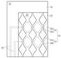
도 1은 실시예에 따른 터치 패널의 개략적인 평면도이다.
도 2는 도 1의 A 부분을 확대하여 도시한 평면도이다.
도 3은 도 1의 B-B'를 따라서 절단한 단면을 도시한 단면도이다.
도 4는 제2 실시예에 따른 터치 패널의 단면도이다.
도 5는 제3 실시예에 따른 터치 패널의 단면도이다.
도 6은 제4 실시예에 따른 터치 패널의 단면도이다.
도 7은 실시예에 따른 터치 패널의 제조 방법의 공정 흐름도이다.1 is a schematic plan view of a touch panel according to an embodiment.
FIG. 2 is an enlarged plan view of portion A of FIG. 1.
3 is a cross-sectional view taken along the line BB ′ of FIG. 1.
4 is a cross-sectional view of a touch panel according to a second embodiment.
5 is a cross-sectional view of a touch panel according to a third embodiment.
6 is a cross-sectional view of a touch panel according to a fourth embodiment.
7 is a process flowchart of a method of manufacturing a touch panel according to an embodiment.
실시예들의 설명에 있어서, 각 층(막), 영역, 패턴 또는 구조물들이 기판, 각 층(막), 영역, 패드 또는 패턴들의 “상/위(on)”에 또는 “하/아래(under)”에 형성된다는 기재는, 직접(directly) 또는 다른 층을 개재하여 형성되는 것을 모두 포함한다. 각 층의 상/위 또는 하/아래에 대한 기준은 도면을 기준으로 설명한다.In the description of embodiments, each layer, region, pattern, or structure may be “on” or “under” the substrate, each layer, region, pad, or pattern. Substrate formed in ”includes all formed directly or through another layer. The criteria for top / bottom or bottom / bottom of each layer are described with reference to the drawings.
도면에서 각 층(막), 영역, 패턴 또는 구조물들의 두께나 크기는 설명의 명확성 및 편의를 위하여 변형될 수 있으므로, 실제 크기를 전적으로 반영하는 것은 아니다.The thickness or the size of each layer (film), region, pattern or structure in the drawings may be modified for clarity and convenience of explanation, and thus does not entirely reflect the actual size.
이하, 첨부한 도면을 참조하여 본 발명의 실시예를 상세하게 설명하면 다음과 같다.Hereinafter, embodiments of the present invention will be described in detail with reference to the accompanying drawings.
먼저 도 1 내지 도 3을 참조하여, 제1 실시예에 따른 터치 패널을 상세하게 설명한다. 도 1은 실시예에 따른 터치 패널의 개략적인 평면도이다. 도 2는 도 1의 A 부분을 확대하여 도시한 평면도이다. 도 3은 도 1의 B-B'를 따라서 절단한 단면을 도시한 단면도이다.First, the touch panel according to the first embodiment will be described in detail with reference to FIGS. 1 to 3. 1 is a schematic plan view of a touch panel according to an embodiment. FIG. 2 is an enlarged plan view of portion A of FIG. 1. 3 is a cross-sectional view taken along the line BB ′ of FIG. 1.
도 1 내지 도 3을 참조하면, 제1 실시예에 따른 터치 패널(100)에는, 입력 장치의 위치를 감지하는 유효 영역(AA)과, 이 유효 영역(AA)의 외곽으로 위치하는 더미 영역(DA)이 정의된다.1 to 3, the
여기서, 유효 영역(AA)에는 입력 장치를 감지할 수 있도록 투명 전극(30)이 형성될 수 있다. 그리고 더미 영역(DA)에는 투명 전극(30)에 연결되는 배선(40) 및 이 배선(40)을 외부 회로(도시하지 않음, 이하 동일)에 연결하는 인쇄 회로 기판 등이 위치할 수 있다. 이러한 더미 영역(DA)에는 외곽 더미층(20)이 형성될 수 있으며, 이 외곽 더미층(20)에는 로고(logo)(20a) 등이 형성될 수 있다. 이러한 터치 패널(100)을 좀더 상세하게 설명하면 다음과 같다.Here, the
제1 실시예에 따른 터치 패널(100)은, 기판(10), 외곽 더미층(20), 광학용 투명 접착제(60), 투명 전극(30), 배선(40), 절연층(50), 투명 전극용 기재(70) 및 반사 방지층(80)을 포함할 수 있다.The
상기 기판(10)은 유리 기판 또는 플라스틱 기판으로 이루어질 수 있다.The
그러나 실시예가 이에 한정되는 것은 아니고, 상기 기판(10)은 곡면성형된 유리(glass)일 수 있다. 따라서, 상기 기판(10)의 적어도 어느 한면은 곡면을 포함할 수 있다. 상기 곡면은 오목한 형상일 수 있다. 또는, 상기 곡면은 볼록한 형상일 수 있다.However, the embodiment is not limited thereto, and the
이를 통해, 실시예에 따른 터치 패널(100)이 적용된 디스플레이 장치는 곡면의 시각적인 안정감을 줄 수 있다. 또한, 상기 터치 패널(100)의 터치감도를 향상시킬 수 있다. 특히, 상기 터치 패널(100)이 핸드폰에 적용되었을 때, 사용성이 향상될 수 있고, 상기 핸드폰을 손에 쥐었을 때 그립감이 좋아 안정감을 줄 수 있다. 또한, 상기 핸드폰으로 통화 시 얼굴 라인에 밀착되는 느낌을 주어 사용감을 향상시킬 수 있다.Through this, the display device to which the
상기 기판(10)과 상기 투명 전극용 기재(70) 사이에 광학용 투명 접착제(60)(optically clear adhesive, OCA)가 위치할 수 있다. 상기 광학용 투명 접착제(60)는 상기 기판(10)과 상기 투명 전극용 기재(70)를 합착할 수 있다. 상기 광학용 투명 접착제(60)는 터치 패널의 투과율을 크게 저하시키지 않으면서도, 상기 기판(10) 및 상기 투명 전극용 기재(70)를 합착할 수 있다.An optically
이어서, 상기 투명 전극용 기재(70)는 상기 기판(10)의 어느 한면에 위치할 수 있다. 상기 투명 전극용 기재(70)는 폴리 에틸렌 테레프탈레이트(poly (ethylene terephthalate), PET) 필름을 포함할 수 있다. 그러나 실시예가 이에 한정되는 것은 아니고, 상기 투명 전극(30)이 형성될 수 있는 다양한 물질을 포함할 수 있다.Subsequently, the
상기 투명 전극(30)은 제1 투명 전극(32) 및 제2 투명 전극(34)을 포함할 수 있다.The
상기 제1 및 제2 투명 전극(32, 34)은 손가락 등의 입력 장치가 접촉되었는지 감지하는 센서부(32a, 34a)와, 이러한 센서부(32a, 34a)를 연결하는 연결부(32b, 34b)를 포함한다. 제1 투명 전극(32)의 연결부(32b)는 센서부(32a)를 제1 방향(도면의 좌우 방향)으로 연결하고, 제2 투명 전극(34)의 연결부(34b)는 센서부(34a)를 제2 방향(도면의 상하 방향)으로 연결한다.The first and second
상기 투명 전극(30)은 손가락 등의 입력 장치가 접촉되었는지를 감지할 수 있는 다양한 형상으로 형성될 수 있다.The
이러한 투명 전극(30)은 광의 투과를 방해하지 않으면서 전기가 흐를 수 있도록 투명 전도성 물질을 포함할 수 있다. 이를 위하여 투명 전극(30)은 인듐 주석 산화물(indium tin oxide), 인듐 아연 산화물(indium zinc oxide), 구리 산화물(copper oxide), 주석 산화물(tin oxide), 아연 산화물(zinc oxide), 티타늄 산화물(titanium oxide) 등의 금속 산화물이나 탄소 나노 튜브(carbon nano tube, CNT), 전도성 고분자 물질 등의 다양한 물질을 포함할 수 있다.The
상기 제1 투명 전극(32) 및 상기 제2 투명 전극(34)이 상기 투명 전극용 기재(70)의 동일한 면에 위치할 수 있다. 구체적으로, 상기 투명 전극용 기재(70)의 일 면에 상기 제2 투명 전극(34)이 위치하고, 상기 제2 투명 전극(34) 상에 상기 제1 투명 전극(32)이 위치할 수 있다.The first
상기 제1 투명 전극(32) 및 상기 제2 투명 전극(34)이 상기 투명 전극용 기재(70)인 폴리 에틸렌 테레프탈레이트(poly(ethylene terephthalate), PET) 필름에 형성되기 때문에, 터치 패널의 유연성(flexibility)을 확보할 수 있다.Since the first
종래에는, 터치 패널의 두께를 줄이고자, 기판(10)에 직접 투명 전극이 형성되었다. 특히, 상기 기판(10)이 곡면을 포함할 경우, 상기 곡면 부분에 위치한 투명 전극의 전기적 특성을 제어하기 어렵다는 문제가 있었다.Conventionally, in order to reduce the thickness of the touch panel, a transparent electrode is formed directly on the
본 실시예에서는 기판(10)에 바로 투명 전극이 형성되는 것이 아니므로, 상기 투명 전극의 전기적 특성을 제어하기 용이하다. 또한, 상기 투명 전극(30)이 상기 투명 전극용 기재(70)에 형성되므로 얇은 두께를 유지할 수 있다.In this embodiment, since the transparent electrode is not formed directly on the
이어서, 상기 제1 투명 전극(32) 및 상기 제2 투명 전극(34) 사이에 절연층(50)이 위치할 수 있다. 즉, 상기 제2 투명 전극(34)에 전면적으로 절연층(50)이 위치될 수 있다. 이로써, 상기 제1 투명 전극(32) 및 상기 제2 투명 전극(34)의 전기적 단락을 방지할 수 있다.Subsequently, an insulating
상기 절연층(50)은 실리콘 산화물과 같은 금속 산화물, 폴리머 및 아크릴계 수지 등으로 이루어질 수 있다.The insulating
이러한 제1 및 제2 투명 전극(32, 34)을 절연층(50)을 사이에 두고 서로 다른 층에 위치시킴으로써 센싱을 더욱 민감하게 할 수 있고 이에 의해 터치의 정확성을 향상할 수 있다. 또한 최근 주목받고 있는 멀티 터치가 가능한 터치 패널을 제공할 수 있다. 특히, 멀치 터치가 가능하고 곡면 글래스(glass)를 적용한 터치 패널을 제공할 수 있다. 멀티 터치는 동시에 여러 개의 터치 포인트를 인식하는 기술로, 일반적인 하나의 터치 포인트만 인식을 하는 것보다 더 다양한 조작을 할 수 있다. 터치를 통해서 위치 변화만 입력할 수 있었기 때문에 다양한 조작을 위하여 보조 단추 같은 별도의 조작이 필요했던 기존의 터치방식과는 달리, 감지되는 터치 포인트의 갯수에 따라 터치에 대한 장치의 반응을 지정할 수도 있고 터치포인트 간격 변화를 통한 조작도 가능하기 때문에 더 직관적이고 쉽고 편하게 조작할 수 있다.By positioning the first and second
상기 투명 전극용 기재(70)는 하드코팅층(도시하지 않음, 이하 동일)을 포함할 수 있고, 상기 하드코팅층 및 상기 절연층(50)이 인덱스 매칭(index matching)될 수 있다. 이러한 인덱스 매칭에 의하여 투과율, 반사율, 색차(b*, yellowish) 특성을 최적화할 수 있다. 더욱이, 인덱스 매칭에 의하여 투명 전도성 물질로 형성된 제1 및 제2 투명 전극(32, 34)을 보이지 않도록(invisible) 할 수 있다. 이에 의하여 터치 패널(100)이 적용된 디스플레이 장치의 시인성을 향상할 수 있다.The
이와 같은 터치 패널(100)에 손가락 등의 입력 장치가 접촉되면, 입력 장치가 접촉된 부분에서 정전 용량의 차이가 발생되고, 이 차이가 발생된 부분을 접촉 위치로 검출할 수 있다.When an input device such as a finger contacts the
기판(10)의 더미 영역(DA)으로 투명 전극(30)에 연결되는 배선(40) 및 이 배선(40)에 연결되는 인쇄 회로 기판(도시하지 않음, 이하 동일)이 형성된다. 이러한 배선(40)은 더미 영역(DA)에 위치하므로 전기 전도성이 우수한 금속으로 이루어질 수 있다. 인쇄 회로 기판으로는 다양한 형태의 인쇄 회로 기판이 적용될 수 있는데, 일례로 플렉서블 인쇄 회로 기판(flexible printed circuit board, FPCB) 등이 적용될 수 있다.A
상기 반사 방지층(80)은 반사에 의한 눈부심이나 화면이 보이지 않는 현상을 막기 위해 가시광 영역의 빛의 반사율을 낮추는 역할을 한다. 즉, 반사 방지층(80)은 반사의 악영향을 효과적으로 감소시켜 우수한 해상도를 제공할 수 있고 시인성을 향상할 수 있다. 또한, 터치 패널(100)의 투과율을 90% 이상, 바람직하게는 92% 이상, 최대로는 99%까지 향상하는 역할을 할 수 있다.The
이러한 반사 방지층(80)은 굴절률이 1.35 내지 2.7인 산화물 또는 불화물을 포함할 수 있다. 이러한 굴절률은 반사 방지에 적합한 범위로 결정된 것이며, 이러한 반사 방지층(80)은 서로 다른 굴절률을 가지는 물질을 한 층 이상 적층하여 형성될 수 있다.The
상기 반사 방지층(80)이 상기 투명 전극용 기재(70)에 밀착하여 형성됨으로써, 터치 패널의 두께를 감소할 수 있다.Since the
도면에 도시하지 않았으나, 상기 투명 전극(30) 및 배선(40)을 덮으면서 비산 방지 필름이 형성될 수 있다. 비산 방지 필름은 터치 패널(100)이 충격에 의해 파손될 때 파편이 비산되는 것을 방지하기 위한 것으로, 다양한 물질 및 구조로 형성될 수 있다.Although not shown in the drawings, a shatterproof film may be formed while covering the
이하, 도 4를 참조하여 제2 실시예에 따른 터치 패널을 좀더 상세하게 설명한다. 명확하고 간략한 설명을 위하여 제1 실시예와 동일 또는 극히 유사한 부분에 대해서는 상세한 설명을 생략하고, 서로 다른 부분만을 상세하게 설명한다.Hereinafter, the touch panel according to the second exemplary embodiment will be described in more detail with reference to FIG. 4. For the sake of clarity and simplicity, detailed descriptions of parts that are the same as or similar to those of the first embodiment will be omitted, and only different parts will be described in detail.
도 4는 제2 실시예에 따른 터치 패널의 단면도이다.4 is a cross-sectional view of a touch panel according to a second embodiment.
제2 실시예에 따른 터치 패널(200)에서는 상기 제1 투명 전극(32) 및 상기 제2 투명 전극(34)이 상기 투명 전극용 기재(70)를 사이에 두고 서로 다른 면에 위치할 수 있다. 즉, 상기 제1 투명 전극(32)이 상기 투명 전극용 기재(70)의 상면에 위치할 수 있고, 상기 제2 투명 전극(34)이 상기 투명 전극용 기재(70)의 하면에 위치할 수 있다.In the
상기 투명 전극용 기재(70)가 상기 제1 투명 전극(32) 및 상기 제2 투명 전극(34)의 전기적 단락을 방지할 수 있다. 따라서, 별도의 절연층을 생략할 수 있다.The transparent
종래에는 투명 전극용 기재(70)에 하나의 투명 전극만이 형성되어 2층(2 layer) 정전 용량 방식의 터치 패널에서는 두 개 이상의 투명 전극용 기재(70) 및 이를 접착하는 다수의 광학용 투명 접착제(60)가 필요하였다. 이에 따라 터치 패널의 두께가 두꺼워지고, 투과율 및 시인성이 저하된다는 문제가 있었다.In the related art, only one transparent electrode is formed on the
본 실시예에서는 하나의 투명 전극용 기재(70)에 제1 및 제 2 투명전극(32, 34)이 모두 형성될 수 있어 이러한 문제점을 개선할 수 있다.In the present exemplary embodiment, both the first and second
또한 이러한 제1 및 제2 투명 전극(32, 34)을 투명 전극용 기재(70)를 사이에 두고 서로 다른 층에 위치시킴으로써 센싱을 더욱 민감하게 할 수 있고 이에 의해 터치의 정확성을 향상할 수 있다.In addition, by placing the first and second
이하 도 5를 참조하여, 제3 실시예예 따른 터치 패널을 설명한다. 명확하고 간략한 설명을 위하여 제1 실시예와 동일 또는 극히 유사한 부분에 대해서는 상세한 설명을 생략하고, 서로 다른 부분만을 상세하게 설명한다.Hereinafter, a touch panel according to a third embodiment will be described with reference to FIG. 5. For the sake of clarity and simplicity, detailed descriptions of parts that are the same as or similar to those of the first embodiment will be omitted, and only different parts will be described in detail.
도 5는 제3 실시예에 따른 터치 패널의 단면도이다.5 is a cross-sectional view of a touch panel according to a third embodiment.
제3 실시예에 따른 터치 패널(300)은 상기 반사 방지층(80)이 반사방지 필름으로 형성될 수 있다. 즉, 상기 반사 방지층(80)이 필름 형태로 형성될 수 있다. 제3 실시예에 따른 터치 패널(300)은 상기 반사 방지층(80)이 필름 형태인 점을 제외하고는 상기 제1 실시예에 따른 터치 패널(100)과 동일할 수 있다.In the
이하, 도 6을 참조하여, 제4 실시예예 따른 터치 패널을 설명한다. 명확하고 간략한 설명을 위하여 제2 실시예와 동일 또는 극히 유사한 부분에 대해서는 상세한 설명을 생략하고, 서로 다른 부분만을 상세하게 설명한다.Hereinafter, the touch panel according to the fourth embodiment will be described with reference to FIG. 6. For the sake of clarity and simplicity, detailed descriptions of parts identical or extremely similar to those of the second embodiment will be omitted, and only different parts will be described in detail.
도 6은 제4 실시예에 따른 터치 패널의 단면도이다.6 is a cross-sectional view of a touch panel according to a fourth embodiment.
제4 실시예에 따른 터치 패널(400)은 상기 상기 반사 방지층(80)이 반사방지 필름으로 형성될 수 있다. 즉, 상기 반사 방지층(80)이 필름 형태로 형성될 수 있다. 제4 실시예에 따른 터치 패널(400)은 상기 반사 방지층(80)이 필름 형태인 점을 제외하고는 상기 제2 실시예에 따른 터치 패널(200)과 동일할 수 있다.In the
도 7을 참조하여, 실시예에 따른 터치 패널의 제조 방법을 설명한다.A method of manufacturing a touch panel according to an embodiment will be described with reference to FIG. 7.
도 7은 실시예에 따른 터치 패널의 제조 방법의 공정 흐름도이다.7 is a process flowchart of a method of manufacturing a touch panel according to an embodiment.
실시예에 따른 터치 패널의 제조 방법은, 기판 및 투명 전극용 기재 준비하는 단계(ST100), 투명 전극을 형성하는 단계(ST200), 배선 전극 물질을 증착하는 단계(ST300) 및 반사 방지층을 형성하는 단계(ST400)를 포함할 수 있다.The method of manufacturing a touch panel according to the embodiment includes preparing a substrate and a substrate for a transparent electrode (ST100), forming a transparent electrode (ST200), depositing a wiring electrode material (ST300), and forming an anti-reflection layer. Step ST400 may be included.
상기 기판 및 투명 전극용 기재를 준비하는 단계(ST100)에서는 기판을 준비할 수 있고, 상기 투명 전극용 기재로는 폴리 에틸렌 테레프탈레이트 필름을 준비할 수 있다. 상기 기판은 곡면을 포함할 수 있다.In the preparing of the substrate and the substrate for the transparent electrode (ST100), a substrate may be prepared, and the polyethylene terephthalate film may be prepared as the substrate for the transparent electrode. The substrate may include a curved surface.
이어서, 상기 투명 전극을 형성하는 단계(ST200)는 상기 투명 전극용 기재에 투명 전극을 형성할 수 있다. 상기 투명 전극을 형성하는 단계(ST200)에서는 일 방향으로 연장되는 제1 투명 전극 및 상기 제1 투명 전극과 교차하는 방향으로 연장되는 제2 투명 전극을 형성하는 단계를 포함할 수 있다.Subsequently, the forming of the transparent electrode (ST200) may form a transparent electrode on the substrate for the transparent electrode. The forming of the transparent electrode (ST200) may include forming a first transparent electrode extending in one direction and a second transparent electrode extending in a direction crossing the first transparent electrode.
도 3 및 도 5를 참조하면, 상기 투명 전극을 형성하는 단계(ST200)는 상기 제1 투명 전극(32) 및 상기 제2 투명 전극(34)이 상기 투명 전극용 기재(70)의 동일한 면에 형성되고, 상기 제1 투명 전극(32) 및 상기 제2 투명 전극(34) 사이에 절연층(50)을 형성하는 단계를 더 포함할 수 있다.3 and 5, the forming of the transparent electrode (ST200) may include forming the transparent electrode on the same side of the
상기 제1 및 제2 투명 전극(32, 34)은 증착 등에 의하여 형성될 수 있는데, 일례로 반응성 스퍼터링에 의하여 형성될 수 있다. 이때, 제1 및 제2 투명 전극(32, 34)이 인듐 주석 산화물로 형성될 경우에, 주석의 함량이 10% 이하일 수 있다. 이에 의하여 투과율을 향상시키고, 이후에 어닐링(annealing) 공정으로 인듐 주석 화합물을 결정화하여 전기 전도도를 향상할 수 있다. 그러나 실시예가 이에 한정되는 것은 아니며 다양한 방법으로 제1 및 제2 투명 전극(32, 34)을 형성할 수 있음은 물론이다.The first and second
상기 절연층을 형성하는 단계는 절연물질을 코팅하는 단계를 포함하고, 상기 절연물질이 유기물을 포함할 수 있다. 상기 코팅하는 단계에서는 습식 코팅이 이루어질 수 있다. 이때 상기 절연물질은 폴리머 또는 아크릴계 수지를 포함할 수 있다.The forming of the insulating layer may include coating an insulating material, and the insulating material may include an organic material. The coating may be a wet coating. In this case, the insulating material may include a polymer or an acrylic resin.
또한, 상기 절연층을 형성하는 단계는 절연물질을 증착하는 단계를 포함하고, 상기 절연물질이 무기물을 포함할 수 있다. 이때, 상기 절연물질은 질화실리콘(SiNx) 또는 산화실리콘(SiO2)을 포함할 수 있다.In addition, the forming of the insulating layer may include depositing an insulating material, and the insulating material may include an inorganic material. In this case, the insulating material may include silicon nitride (SiNx ) or silicon oxide (SiO2 ).
이어서, 배선 전극 물질을 증착하는 단계(ST300)는 상기 투명 전극용 기재에서 이루어질 수 있다. 이 단계에서 배선 전극 물질은 앞서 설명한 투명 전극 형성 방법과 동일한 방법으로 증착할 수 있다. 따라서, 배선 전극 물질은 스퍼터링 또는 반응성 스퍼터링의 방법으로 증착할 수 있다. 반응성 스퍼터링 공정으로 배선 전극을 형성할 경우, 산소 또는 질소의 분위기에서 진행될 수 있다.Subsequently, the deposition of the wiring electrode material (ST300) may be performed on the transparent electrode substrate. In this step, the wiring electrode material may be deposited by the same method as the method of forming the transparent electrode. Thus, the wiring electrode material can be deposited by the method of sputtering or reactive sputtering. When the wiring electrode is formed by the reactive sputtering process, it may proceed in an atmosphere of oxygen or nitrogen.
배선 전극 물질은 크롬(Cr), 알루미늄(Al), 은(Ag), 구리(Cu). 니켈(Ni) 및 몰리브덴(Mo) 또는 이들을 포함하는 합금을 포함할 수 있다,The wiring electrode materials are chromium (Cr), aluminum (Al), silver (Ag) and copper (Cu). Nickel (Ni) and molybdenum (Mo) or an alloy containing them,
그러나 실시예가 이에 한정되는 것은 아니므로, 배선 전극 물질이 크롬(Cr) 산화물, 알루미늄(Al) 산화물, 은(Ag) 산화물, 구리(Cu) 산화물. 니켈(Ni) 산화물 및 몰리브덴(Mo) 산화물을 포함할 수 있다.However, the embodiment is not limited thereto, and the wiring electrode material may be chromium (Cr) oxide, aluminum (Al) oxide, silver (Ag) oxide, or copper (Cu) oxide. It may include nickel (Ni) oxide and molybdenum (Mo) oxide.
배선 전극 물질을 증착하는 단계(ST300)이후에, 상기 배선 전극 물질을 에칭하여 배선 전극을 형성하는 단계를 더 포함할 수 있다. 구체적으로, 배선 전극 물질을 습식 식각(wet etching)의 방법으로 형성할 수 있다. 습식 식각은 화학 약품을 이용하는 방법으로, 화학 약품내에 포함된 성분이 에칭하고자 하는 물질과 화학 반응을 일으켜 에칭하고자 하는 성분이 약품 용액 중에 녹아내리면서 에칭되는 기술을 말한다. 일례로, 본 실시예에서는, FeCl3 수용액 또는 NaOH 수용액을 이용하여 에칭할 수 있다.After depositing the wiring electrode material (ST300), the method may further include etching the wiring electrode material to form the wiring electrode. Specifically, the wiring electrode material may be formed by wet etching. Wet etching is a method of using a chemical, and refers to a technique in which a component contained in a chemical chemically reacts with a substance to be etched and is etched while the component to be etched is dissolved in a chemical solution. For example, in this embodiment, it can be etched using FeCl3 aqueous solution or NaOH aqueous solution.
이러한 습식 식각 방법을 통해 얇은 선폭을 가지는 배선 전극을 형성할 수 있다. 구체적으로, 배선 전극의 선폭이 10 um 내지 100 um 가 될 수 있다.Through the wet etching method, a wiring electrode having a thin line width can be formed. Specifically, the line width of the wiring electrode may be 10 um to 100 um.
본 실시예에서는 배선 전극의 선폭을 얇게 형성하여 좁은 더미 영역을 구현할 수 있다. 일례로, 더미 영역(도 1의 참조 부호 DA, 이하 동일)이 2 mm로 형성되어 터치 패널의 유효 영역(도 1의 참조 부호 AA, 이하 동일) 및 디자인의 다양성을 확보할 수 있다. 또한, 배선 전극의 선폭이 얇기 때문에, 더미 영역(DA)내에서 많은 수의 배선 전극이 형성될 수 있어 터치 패널의 해상도를 높일 수 있다.In this embodiment, a narrow dummy region may be realized by forming a thin line width of the wiring electrode. For example, a dummy area (reference numeral DA of FIG. 1, hereinafter identical) is formed to be 2 mm, thereby securing a variety of designs and an effective area of the touch panel (reference numeral AA of FIG. 1, hereinafter identical). In addition, since the line width of the wiring electrode is thin, a large number of wiring electrodes can be formed in the dummy area DA, so that the resolution of the touch panel can be increased.
종래에는 배선 전극 형성 시 인쇄 공정으로 형성하였고, 이러한 인쇄 공정으로 형성할 경우, 100 um 이하의 선폭 구현이 어려웠다. 따라서, 넓은 선폭을 가지는 배선 전극을 가리기 위해 적어도 5 내지 10 mm 의 더미 영역(DA)이 필요하였다. 이로 인해 유효 영역(AA)이 줄어들고 디자인에 제약이 있다는 문제점이 있었다.Conventionally, the wiring electrode was formed by a printing process, and when formed by such a printing process, it was difficult to realize a line width of 100 um or less. Therefore, at least 5 to 10 mm of dummy area DA was required to cover the wiring electrode having a wide line width. As a result, there is a problem that the effective area (AA) is reduced and the design is limited.
이어서, 상기 반사 방지층을 형성하는 단계(ST400)는 반사방지물질을 코팅하는 단계를 포함할 수 있다.Subsequently, the forming of the antireflective layer (ST400) may include coating an antireflective material.
도 3 및 도 4를 참조하면, 상기 반사 방지층(80)이 코팅으로 형성되어 상기 투명 전극용 기재(70)에 밀착하여 형성될 수 있다. 따라서, 터치 패널의 두께를 감소할 수 있다.3 and 4, the
그러나 실시예가 이에 한정되는 것은 아니고, 상기 반사 방지층을 형성하는 단계(ST400)는 반사방지 필름을 형성하는 단계를 포함할 수 있다.However, the embodiment is not limited thereto, and the forming of the antireflective layer (ST400) may include forming an antireflective film.
도 5 및 도 6을 참조하면, 상기 투명 전극용 기재(70)의 하면에 반사방지 필름이 형성될 수 있다.5 and 6, an anti-reflection film may be formed on the lower surface of the
상술한 실시예에 설명된 특징, 구조, 효과 등은 본 발명의 적어도 하나의 실시예에 포함되며, 반드시 하나의 실시예에만 한정되는 것은 아니다. 나아가, 각 실시예에서 예시된 특징, 구조, 효과 등은 실시예들이 속하는 분야의 통상의 지식을 가지는 자에 의하여 다른 실시예들에 대해서도 조합 또는 변형되어 실시 가능하다. 따라서 이러한 조합과 변형에 관계된 내용들은 본 발명의 범위에 포함되는 것으로 해석되어야 할 것이다.The features, structures, effects and the like described in the foregoing embodiments are included in at least one embodiment of the present invention and are not necessarily limited to one embodiment. Further, the features, structures, effects, and the like illustrated in the embodiments may be combined or modified in other embodiments by those skilled in the art to which the embodiments belong. Therefore, it should be understood that the present invention is not limited to these combinations and modifications.
또한, 이상에서 실시예들을 중심으로 설명하였으나 이는 단지 예시일 뿐 본 발명을 한정하는 것이 아니며, 본 발명이 속하는 분야의 통상의 지식을 가진 자라면 본 실시예의 본질적인 특성을 벗어나지 않는 범위에서 이상에 예시되지 않은 여러 가지의 변형과 응용이 가능함을 알 수 있을 것이다. 예를 들어, 실시예들에 구체적으로 나타난 각 구성 요소는 변형하여 실시할 수 있는 것이다. 그리고 이러한 변형과 응용에 관계된 차이점들은 첨부한 청구 범위에서 규정하는 본 발명의 범위에 포함되는 것으로 해석되어야 할 것이다.While the present invention has been particularly shown and described with reference to exemplary embodiments thereof, it is clearly understood that the same is by way of illustration and example only and is not to be construed as limiting the scope of the present invention. It can be seen that various modifications and applications are possible. For example, each component specifically shown in the embodiments may be modified. It is to be understood that the present invention may be embodied in many other specific forms without departing from the spirit or essential characteristics thereof.
Claims (18)
Translated fromKorean상기 기판의 어느 한 면에 위치하고, 투명 전극이 위치하는 투명 전극용 기재;
상기 투명 전극용 기재의 어느 한면에 위치하고, 일 방향으로 연장되는 제1 투명 전극; 및
상기 투명 전극용 기재의 어느 한면에 위치하고, 상기 제1 투명 전극과 교차하는 방향으로 연장되는 제2 투명 전극을 포함하고,
상기 투명 전극용 기재는 상기 기판과 이격되어 배치되고,
상기 제1 투명 전극과 상기 제2 투명 전극은 서로 다른 층에 배치되는 터치 패널.At least one side of the substrate comprises a curved surface;
A substrate for transparent electrodes positioned on one surface of the substrate and having transparent electrodes;
A first transparent electrode positioned on one surface of the substrate for transparent electrode and extending in one direction; And
A second transparent electrode positioned on one surface of the substrate for transparent electrode and extending in a direction crossing the first transparent electrode;
The substrate for transparent electrode is disposed spaced apart from the substrate,
The first transparent electrode and the second transparent electrode are disposed on different layers.
상기 제1 투명 전극 및 상기 제2 투명 전극이 상기 투명 전극용 기재의 동일한 면에 위치하고, 상기 제1 투명 전극 및 상기 제2 투명 전극 사이에 절연층이 위치하는 터치 패널.The method of claim 1,
And the first transparent electrode and the second transparent electrode are located on the same side of the substrate for the transparent electrode, and an insulating layer is positioned between the first transparent electrode and the second transparent electrode.
상기 투명 전극용 기재는 하드코팅층을 포함하고,
상기 하드코팅층 및 상기 절연층이 인덱스 매칭되는 터치 패널.The method of claim 2,
The transparent electrode base material includes a hard coating layer,
And the hard coating layer and the insulating layer are index matched.
상기 제1 투명 전극 및 상기 제2 투명 전극은 상기 투명 전극용 기재의 서로 반대되는 면에 위치하는 터치 패널.The method of claim 1,
The first transparent electrode and the second transparent electrode are located on opposite surfaces of the substrate for transparent electrode.
상기 투명 전극용 기재는 폴리 에틸렌 테레프탈레이트(poly(ethylene terephthalate), PET) 필름을 포함하는 터치 패널.The method of claim 1,
The transparent electrode substrate is a touch panel comprising a polyethylene terephthalate (poly (ethylene terephthalate), PET) film.
상기 투명 전극용 기재의 어느 한 면에 위치하는 반사방지층을 더 포함하는 터치 패널.The method of claim 1,
The touch panel further comprises an anti-reflection layer located on one side of the substrate for transparent electrode.
상기 기판 및 상기 투명 전극용 기재 사이에 광학용 투명 접착제(optically clear adhesive, OCA)가 포함되는 터치 패널.The method of claim 1,
An optically clear adhesive (OCA) is included between the substrate and the substrate for transparent electrode.
상기 기판의 적어도 어느 한 면은 곡면을 포함하는 터치 패널.The method of claim 1,
At least one surface of the substrate comprises a curved surface.
상기 투명 전극용 기재에 투명 전극을 형성하는 단계;
상기 투명 전극용 기재에 배선 전극 물질을 증착하는 단계; 및
상기 투명 전극용 기재에 반사방지층을 형성하는 단계를 포함하고,
상기 투명 전극을 형성하는 단계는 일 방향으로 연장되는 제1 투명 전극 및 상기 제1 투명 전극과 교차하는 방향으로 연장되는 제2 투명 전극을 형성하는 단계를 포함하고,
상기 제1 투명 전극과 상기 제2 투명 전극은 서로 다른 층에 배치되는 터치 패널의 제조 방법.Preparing at least one surface of the substrate including a curved surface and a substrate for the transparent electrode spaced apart from the substrate;
Forming a transparent electrode on the substrate for the transparent electrode;
Depositing a wiring electrode material on the transparent electrode substrate; And
Forming an anti-reflection layer on the transparent electrode substrate;
The forming of the transparent electrode includes forming a first transparent electrode extending in one direction and a second transparent electrode extending in a direction crossing the first transparent electrode,
The first transparent electrode and the second transparent electrode is a manufacturing method of the touch panel disposed on different layers.
상기 투명 전극을 형성하는 단계는 일 방향으로 연장되는 제1 투명 전극 및 상기 제1 투명 전극과 교차하는 방향으로 연장되는 제2 투명 전극을 형성하는 단계를 포함하는 터치 패널의 제조 방법.10. The method of claim 9,
The forming of the transparent electrode may include forming a first transparent electrode extending in one direction and a second transparent electrode extending in a direction crossing the first transparent electrode.
상기 투명 전극을 형성하는 단계는 상기 제1 투명 전극 및 상기 제2 투명 전극이 상기 투명 전극용 기재의 동일한 면에 형성되고, 상기 제1 투명 전극 및 상기 제2 투명 전극 사이에 절연층을 형성하는 단계를 더 포함하는 터치 패널의 제조 방법.The method of claim 10,
The forming of the transparent electrode may include forming the insulating layer between the first transparent electrode and the second transparent electrode on the same surface of the substrate for the transparent electrode, and forming the insulating layer between the first transparent electrode and the second transparent electrode. Method of manufacturing a touch panel further comprising the step.
상기 절연층을 형성하는 단계는 절연물질을 코팅하는 단계를 포함하고, 상기 절연물질이 유기물을 포함하는 터치 패널의 제조 방법.12. The method of claim 11,
The forming of the insulating layer may include coating an insulating material, and the insulating material includes an organic material.
상기 절연층을 형성하는 단계는 절연물질을 증착하는 단계를 포함하고, 상기 절연물질이 무기물을 포함하는 터치 패널의 제조 방법.12. The method of claim 11,
The forming of the insulating layer may include depositing an insulating material, and the insulating material includes an inorganic material.
상기 투명 전극용 기재는 하드코팅층을 포함하고,
상기 하드코팅층 및 상기 절연층이 인덱스 매칭되는 터치 패널의 제조 방법.12. The method of claim 11,
The transparent electrode base material includes a hard coating layer,
The hard coating layer and the insulating layer is a manufacturing method of the touch panel index matching.
상기 배선 전극 물질을 증착하는 단계 이후에, 상기 배선 전극 물질을 에칭하여 배선 전극을 형성하는 단계를 더 포함하는 터치 패널의 제조 방법.10. The method of claim 9,
After depositing the wiring electrode material, etching the wiring electrode material to form a wiring electrode.
상기 배선 전극의 선폭이 10 um 내지 100 um 인 터치 패널의 제조 방법.16. The method of claim 15,
The line width of the said wiring electrode is a manufacturing method of the touch panel of 10um-100um.
상기 반사방지층을 형성하는 단계는 반사방지물질을 코팅하는 단계를 포함하는 터치 패널의 제조 방법.10. The method of claim 9,
Forming the anti-reflective layer comprises the step of coating an anti-reflective material.
상기 반사방지층을 형성하는 단계는 반사방지 필름을 형성하는 단계를 포함하는 터치 패널의 제조 방법.10. The method of claim 9,
Forming the anti-reflection layer comprises the step of forming an anti-reflection film.
Priority Applications (12)
| Application Number | Priority Date | Filing Date | Title |
|---|---|---|---|
| KR1020110064111AKR101294569B1 (en) | 2011-06-29 | 2011-06-29 | Touch panel and method for manufacturing the same |
| JP2014518811AJP6185462B2 (en) | 2011-06-29 | 2012-06-29 | Touch panel and manufacturing method thereof |
| PCT/KR2012/005200WO2013002609A2 (en) | 2011-06-29 | 2012-06-29 | Touch panel and method for manufacturing the same |
| CN201711157929.5ACN107885401B (en) | 2011-06-29 | 2012-06-29 | Touch panel and method for manufacturing the same |
| TW101123571ATWI612458B (en) | 2011-06-29 | 2012-06-29 | Touch panel and method for manufacturing the same |
| CN201280042477.5ACN103765359B (en) | 2011-06-29 | 2012-06-29 | Touch panel and method for manufacturing same |
| EP12805392.3AEP2726964B1 (en) | 2011-06-29 | 2012-06-29 | Touch panel and method for manufacturing the same |
| US14/130,259US9433089B2 (en) | 2011-06-29 | 2012-06-29 | Touch panel and method for manufacturing the same |
| US15/222,541US9933890B2 (en) | 2011-06-29 | 2016-07-28 | Touch panel and method for manufacturing the same |
| US15/792,383US10088948B2 (en) | 2011-06-29 | 2017-10-24 | Touch panel and method for manufacturing the same |
| US16/059,754US10310666B2 (en) | 2011-06-29 | 2018-08-09 | Touch panel and method for manufacturing the same |
| US16/393,189US10592043B2 (en) | 2011-06-29 | 2019-04-24 | Touch panel and method for manufacturing the same |
Applications Claiming Priority (1)
| Application Number | Priority Date | Filing Date | Title |
|---|---|---|---|
| KR1020110064111AKR101294569B1 (en) | 2011-06-29 | 2011-06-29 | Touch panel and method for manufacturing the same |
Publications (2)
| Publication Number | Publication Date |
|---|---|
| KR20130002885A KR20130002885A (en) | 2013-01-08 |
| KR101294569B1true KR101294569B1 (en) | 2013-08-07 |
Family
ID=47424710
Family Applications (1)
| Application Number | Title | Priority Date | Filing Date |
|---|---|---|---|
| KR1020110064111AActiveKR101294569B1 (en) | 2011-06-29 | 2011-06-29 | Touch panel and method for manufacturing the same |
Country Status (7)
| Country | Link |
|---|---|
| US (5) | US9433089B2 (en) |
| EP (1) | EP2726964B1 (en) |
| JP (1) | JP6185462B2 (en) |
| KR (1) | KR101294569B1 (en) |
| CN (2) | CN103765359B (en) |
| TW (1) | TWI612458B (en) |
| WO (1) | WO2013002609A2 (en) |
Families Citing this family (17)
| Publication number | Priority date | Publication date | Assignee | Title |
|---|---|---|---|---|
| KR101294569B1 (en) | 2011-06-29 | 2013-08-07 | 엘지이노텍 주식회사 | Touch panel and method for manufacturing the same |
| CN103576950B (en)* | 2012-07-24 | 2016-08-24 | 宸鸿科技(厦门)有限公司 | Contact panel and preparation method thereof |
| US9213781B1 (en) | 2012-09-19 | 2015-12-15 | Placemeter LLC | System and method for processing image data |
| JP2014194749A (en)* | 2013-02-27 | 2014-10-09 | Hosiden Corp | Touch panel |
| WO2015184440A2 (en) | 2014-05-30 | 2015-12-03 | Placemeter Inc. | System and method for activity monitoring using video data |
| JP6639098B2 (en)* | 2015-03-20 | 2020-02-05 | 富士フイルム株式会社 | Touch panel member, touch panel, and touch panel display device |
| US10043078B2 (en) | 2015-04-21 | 2018-08-07 | Placemeter LLC | Virtual turnstile system and method |
| US10380431B2 (en) | 2015-06-01 | 2019-08-13 | Placemeter LLC | Systems and methods for processing video streams |
| KR102555153B1 (en)* | 2015-12-03 | 2023-07-14 | 삼성디스플레이 주식회사 | Touch panel |
| KR102513362B1 (en) | 2015-12-11 | 2023-03-24 | 삼성디스플레이 주식회사 | Liquid crystal display panel and method of manufacturing the same |
| CN105630263A (en)* | 2015-12-22 | 2016-06-01 | 昆山国显光电有限公司 | Touch panel, touch display screen as well as manufacturing method and equipment of touch panel |
| CN108022565B (en)* | 2016-11-02 | 2021-03-30 | 群创光电股份有限公司 | Adjusting method and display |
| US11042254B2 (en)* | 2016-11-02 | 2021-06-22 | Innolux Corporation | Touch display devices |
| WO2018199402A1 (en) | 2017-04-24 | 2018-11-01 | 엘지전자 주식회사 | Curved glass manufacturing method |
| CN109212802B (en)* | 2017-07-06 | 2021-05-18 | 京东方科技集团股份有限公司 | Touch panel, preparation method thereof and display device |
| KR102218695B1 (en)* | 2018-09-17 | 2021-02-19 | 동우 화인켐 주식회사 | Touch sensor and method of manufacturing the same |
| KR102361287B1 (en)* | 2019-04-29 | 2022-02-11 | 주식회사 아모그린텍 | Touch screen panel and method for manufacturing the same |
Citations (3)
| Publication number | Priority date | Publication date | Assignee | Title |
|---|---|---|---|---|
| KR20080096976A (en)* | 2007-04-30 | 2008-11-04 | 안영수 | Capacitive touch screen and manufacturing method |
| KR100942763B1 (en)* | 2009-03-30 | 2010-02-18 | (주) 월드비젼 | Capacitive touch sensor integrated with window panel and mathod for manufacturing there of |
| KR20100124365A (en)* | 2009-05-19 | 2010-11-29 | 일진디스플레이(주) | Upper plate for touch panel |
Family Cites Families (37)
| Publication number | Priority date | Publication date | Assignee | Title |
|---|---|---|---|---|
| US4412213A (en) | 1978-11-30 | 1983-10-25 | Futaba Denshi Kogyo K.K. | Driving circuit for a fluorescent display apparatus having fewer leads |
| US4686332A (en) | 1986-06-26 | 1987-08-11 | International Business Machines Corporation | Combined finger touch and stylus detection system for use on the viewing surface of a visual display device |
| JPS576882A (en)* | 1980-06-16 | 1982-01-13 | Hitachi Ltd | Liquid crystal display element |
| JPH11134100A (en)* | 1997-10-31 | 1999-05-21 | Alps Electric Co Ltd | Coordinate input device and production thereof |
| CN1145089C (en)* | 1999-03-25 | 2004-04-07 | 时至准钟表股份有限公司 | Timepiece with liquid crystal display panel |
| US6436265B1 (en)* | 1999-03-29 | 2002-08-20 | Canon Kabushiki Kaisha | Microstructure array, and apparatus and method for forming the microstructure array, and a mold for fabricating a microstructure array |
| US6787253B2 (en)* | 2001-06-27 | 2004-09-07 | Bridgestone Corporation | Transparent electroconductive film and touch panel |
| JP2004240548A (en)* | 2003-02-04 | 2004-08-26 | Asahi Glass Co Ltd | Cover glass for pen input device |
| JP2008090517A (en)* | 2006-09-29 | 2008-04-17 | Pentel Corp | Manufacturing method of coordinate input panel |
| CN100582875C (en)* | 2007-04-13 | 2010-01-20 | 群康科技(深圳)有限公司 | Touch screen display apparatus |
| JP5094250B2 (en)* | 2007-07-10 | 2012-12-12 | 株式会社ジャパンディスプレイイースト | Display device |
| US8022939B2 (en) | 2007-10-12 | 2011-09-20 | Epson Imaging Devices Corporation | Touch panel, electro optical device, and electronic apparatus |
| US8629841B2 (en) | 2008-04-30 | 2014-01-14 | Apple Inc. | Multi-touch sensor patterns and stack-ups |
| CN102047207B (en)* | 2008-05-29 | 2013-10-02 | 日本写真印刷株式会社 | Protection panel having touch input function |
| JP2010061425A (en)* | 2008-09-04 | 2010-03-18 | Hitachi Displays Ltd | Touch panel and display device using the same |
| CN101727249B (en) | 2008-10-31 | 2012-02-01 | 宸鸿光电科技股份有限公司 | Manufacturing method of curved capacitive touch panel |
| KR101521219B1 (en) | 2008-11-10 | 2015-05-18 | 엘지전자 주식회사 | Mobile terminal using flexible display and operation method thereof |
| US8982051B2 (en) | 2009-03-30 | 2015-03-17 | Microsoft Technology Licensing, Llc | Detecting touch on a surface |
| JP4958020B2 (en) | 2009-03-31 | 2012-06-20 | 大日本印刷株式会社 | Touch panel sensor, laminate for manufacturing touch panel sensor, and method for manufacturing touch panel sensor |
| CN101989141A (en)* | 2009-07-30 | 2011-03-23 | 胜华科技股份有限公司 | touch display device |
| JP2011059834A (en)* | 2009-09-08 | 2011-03-24 | Hosiden Corp | Touch panel and electronic equipment |
| JP5359736B2 (en)* | 2009-09-28 | 2013-12-04 | 大日本印刷株式会社 | Electrode film for touch panel and touch panel |
| JP2011095903A (en)* | 2009-10-28 | 2011-05-12 | Applied Vacuum Coating Technologies Co Ltd | Touch pad structure |
| TWI386713B (en) | 2009-11-02 | 2013-02-21 | Au Optronics Corp | Touch sensing panel |
| WO2011070801A1 (en)* | 2009-12-10 | 2011-06-16 | 凸版印刷株式会社 | Conductive substrate, method for producing same, and touch panel |
| KR101048948B1 (en) | 2010-02-22 | 2011-07-12 | 삼성모바일디스플레이주식회사 | Manufacturing Method of Touch Screen Panel |
| KR101049006B1 (en) | 2010-02-22 | 2011-07-12 | 삼성모바일디스플레이주식회사 | Touch screen panel and its manufacturing method |
| CN201689397U (en)* | 2010-02-23 | 2010-12-29 | 禾威科技股份有限公司 | Touch module |
| KR101113457B1 (en) | 2010-05-10 | 2012-03-05 | 삼성모바일디스플레이주식회사 | Curved Touch Screen Panel and Fabricating Method for the Same |
| WO2012015284A2 (en)* | 2010-07-30 | 2012-02-02 | Lg Innotek Co., Ltd. | Touch panel |
| CN101963864B (en)* | 2010-10-14 | 2013-03-13 | 北京富纳特创新科技有限公司 | Touch screen |
| CN101976164B (en)* | 2010-10-18 | 2013-06-05 | 汕头超声显示器有限公司 | Capacitor touch screen |
| TWI537778B (en)* | 2011-04-06 | 2016-06-11 | Sitronix Technology Corp | Touch panel sensing structure |
| KR101294569B1 (en)* | 2011-06-29 | 2013-08-07 | 엘지이노텍 주식회사 | Touch panel and method for manufacturing the same |
| CN103092387B (en)* | 2011-10-27 | 2016-08-03 | 宸鸿科技(厦门)有限公司 | Contact panel |
| KR102178797B1 (en)* | 2013-10-04 | 2020-11-16 | 삼성디스플레이 주식회사 | Display device comprising touch sensors |
| JP6302741B2 (en)* | 2013-12-19 | 2018-03-28 | 株式会社ジャパンディスプレイ | Display device |
- 2011
- 2011-06-29KRKR1020110064111Apatent/KR101294569B1/enactiveActive
- 2012
- 2012-06-29CNCN201280042477.5Apatent/CN103765359B/enactiveActive
- 2012-06-29EPEP12805392.3Apatent/EP2726964B1/enactiveActive
- 2012-06-29WOPCT/KR2012/005200patent/WO2013002609A2/enactiveApplication Filing
- 2012-06-29TWTW101123571Apatent/TWI612458B/enactive
- 2012-06-29CNCN201711157929.5Apatent/CN107885401B/enactiveActive
- 2012-06-29USUS14/130,259patent/US9433089B2/enactiveActive
- 2012-06-29JPJP2014518811Apatent/JP6185462B2/enactiveActive
- 2016
- 2016-07-28USUS15/222,541patent/US9933890B2/enactiveActive
- 2017
- 2017-10-24USUS15/792,383patent/US10088948B2/enactiveActive
- 2018
- 2018-08-09USUS16/059,754patent/US10310666B2/enactiveActive
- 2019
- 2019-04-24USUS16/393,189patent/US10592043B2/enactiveActive
Patent Citations (3)
| Publication number | Priority date | Publication date | Assignee | Title |
|---|---|---|---|---|
| KR20080096976A (en)* | 2007-04-30 | 2008-11-04 | 안영수 | Capacitive touch screen and manufacturing method |
| KR100942763B1 (en)* | 2009-03-30 | 2010-02-18 | (주) 월드비젼 | Capacitive touch sensor integrated with window panel and mathod for manufacturing there of |
| KR20100124365A (en)* | 2009-05-19 | 2010-11-29 | 일진디스플레이(주) | Upper plate for touch panel |
Also Published As
| Publication number | Publication date |
|---|---|
| US9433089B2 (en) | 2016-08-30 |
| TW201305890A (en) | 2013-02-01 |
| US10088948B2 (en) | 2018-10-02 |
| EP2726964A2 (en) | 2014-05-07 |
| US9933890B2 (en) | 2018-04-03 |
| US20180046315A1 (en) | 2018-02-15 |
| KR20130002885A (en) | 2013-01-08 |
| WO2013002609A2 (en) | 2013-01-03 |
| US20160334927A1 (en) | 2016-11-17 |
| CN107885401B (en) | 2020-12-22 |
| JP6185462B2 (en) | 2017-08-23 |
| US20140333850A1 (en) | 2014-11-13 |
| CN103765359A (en) | 2014-04-30 |
| WO2013002609A3 (en) | 2013-04-11 |
| CN107885401A (en) | 2018-04-06 |
| TWI612458B (en) | 2018-01-21 |
| US20190250761A1 (en) | 2019-08-15 |
| CN103765359B (en) | 2017-12-26 |
| EP2726964B1 (en) | 2020-02-19 |
| US10310666B2 (en) | 2019-06-04 |
| US20180348952A1 (en) | 2018-12-06 |
| JP2014523030A (en) | 2014-09-08 |
| EP2726964A4 (en) | 2015-03-25 |
| US10592043B2 (en) | 2020-03-17 |
Similar Documents
| Publication | Publication Date | Title |
|---|---|---|
| KR101294569B1 (en) | Touch panel and method for manufacturing the same | |
| US10120229B2 (en) | Touch panel and method for manufacturing the same | |
| JP4874145B2 (en) | Transparent sheet and transparent touch switch | |
| US9891656B2 (en) | Touch panel and method for manufacturing the same | |
| JP2016514873A (en) | Transparent electrode pattern laminate and touch screen panel provided with the same | |
| US20150169104A1 (en) | Touch panel | |
| KR101241632B1 (en) | Method for manufacturing touch panel | |
| KR101386333B1 (en) | Input device and manufacturing method thereof | |
| KR101199138B1 (en) | Touch panel | |
| CN105468184B (en) | Transparent electrode laminate and touch screen panel including the same | |
| KR20120127984A (en) | Capacitive touch screen panel using multi-layer thin film and manufacturing process thereof | |
| KR102008736B1 (en) | Touch panel and method for driving the same | |
| KR20240129787A (en) | Foldable Touch Panel And Manufacturing Methods Thereof |
Legal Events
| Date | Code | Title | Description |
|---|---|---|---|
| A201 | Request for examination | ||
| PA0109 | Patent application | St.27 status event code:A-0-1-A10-A12-nap-PA0109 | |
| PA0201 | Request for examination | St.27 status event code:A-1-2-D10-D11-exm-PA0201 | |
| PE0902 | Notice of grounds for rejection | St.27 status event code:A-1-2-D10-D21-exm-PE0902 | |
| PG1501 | Laying open of application | St.27 status event code:A-1-1-Q10-Q12-nap-PG1501 | |
| P11-X000 | Amendment of application requested | St.27 status event code:A-2-2-P10-P11-nap-X000 | |
| P13-X000 | Application amended | St.27 status event code:A-2-2-P10-P13-nap-X000 | |
| E701 | Decision to grant or registration of patent right | ||
| PE0701 | Decision of registration | St.27 status event code:A-1-2-D10-D22-exm-PE0701 | |
| GRNT | Written decision to grant | ||
| PR0701 | Registration of establishment | St.27 status event code:A-2-4-F10-F11-exm-PR0701 | |
| PR1002 | Payment of registration fee | St.27 status event code:A-2-2-U10-U11-oth-PR1002 Fee payment year number:1 | |
| PG1601 | Publication of registration | St.27 status event code:A-4-4-Q10-Q13-nap-PG1601 | |
| PN2301 | Change of applicant | St.27 status event code:A-5-5-R10-R13-asn-PN2301 St.27 status event code:A-5-5-R10-R11-asn-PN2301 | |
| FPAY | Annual fee payment | Payment date:20160707 Year of fee payment:4 | |
| PR1001 | Payment of annual fee | St.27 status event code:A-4-4-U10-U11-oth-PR1001 Fee payment year number:4 | |
| R18-X000 | Changes to party contact information recorded | St.27 status event code:A-5-5-R10-R18-oth-X000 | |
| FPAY | Annual fee payment | Payment date:20170704 Year of fee payment:5 | |
| PR1001 | Payment of annual fee | St.27 status event code:A-4-4-U10-U11-oth-PR1001 Fee payment year number:5 | |
| FPAY | Annual fee payment | Payment date:20180710 Year of fee payment:6 | |
| PR1001 | Payment of annual fee | St.27 status event code:A-4-4-U10-U11-oth-PR1001 Fee payment year number:6 | |
| R18-X000 | Changes to party contact information recorded | St.27 status event code:A-5-5-R10-R18-oth-X000 | |
| FPAY | Annual fee payment | Payment date:20190711 Year of fee payment:7 | |
| PR1001 | Payment of annual fee | St.27 status event code:A-4-4-U10-U11-oth-PR1001 Fee payment year number:7 | |
| R18-X000 | Changes to party contact information recorded | St.27 status event code:A-5-5-R10-R18-oth-X000 | |
| PR1001 | Payment of annual fee | St.27 status event code:A-4-4-U10-U11-oth-PR1001 Fee payment year number:8 | |
| PN2301 | Change of applicant | St.27 status event code:A-5-5-R10-R13-asn-PN2301 St.27 status event code:A-5-5-R10-R11-asn-PN2301 | |
| P22-X000 | Classification modified | St.27 status event code:A-4-4-P10-P22-nap-X000 | |
| PR1001 | Payment of annual fee | St.27 status event code:A-4-4-U10-U11-oth-PR1001 Fee payment year number:9 | |
| PR1001 | Payment of annual fee | St.27 status event code:A-4-4-U10-U11-oth-PR1001 Fee payment year number:10 | |
| PR1001 | Payment of annual fee | St.27 status event code:A-4-4-U10-U11-oth-PR1001 Fee payment year number:11 | |
| PR1001 | Payment of annual fee | St.27 status event code:A-4-4-U10-U11-oth-PR1001 Fee payment year number:12 | |
| PR1001 | Payment of annual fee | St.27 status event code:A-4-4-U10-U11-oth-PR1001 Fee payment year number:13 |