KR101294449B1 - Integrated circuits and manufacturing methods thereof - Google Patents
Integrated circuits and manufacturing methods thereofDownload PDFInfo
- Publication number
- KR101294449B1 KR101294449B1KR1020110078272AKR20110078272AKR101294449B1KR 101294449 B1KR101294449 B1KR 101294449B1KR 1020110078272 AKR1020110078272 AKR 1020110078272AKR 20110078272 AKR20110078272 AKR 20110078272AKR 101294449 B1KR101294449 B1KR 101294449B1
- Authority
- KR
- South Korea
- Prior art keywords
- metal structure
- diffusion region
- metal
- region
- distance
- Prior art date
- Legal status (The legal status is an assumption and is not a legal conclusion. Google has not performed a legal analysis and makes no representation as to the accuracy of the status listed.)
- Active
Links
Images


Classifications
- H—ELECTRICITY
- H10—SEMICONDUCTOR DEVICES; ELECTRIC SOLID-STATE DEVICES NOT OTHERWISE PROVIDED FOR
- H10D—INORGANIC ELECTRIC SEMICONDUCTOR DEVICES
- H10D64/00—Electrodes of devices having potential barriers
- H10D64/20—Electrodes characterised by their shapes, relative sizes or dispositions
- H10D64/27—Electrodes not carrying the current to be rectified, amplified, oscillated or switched, e.g. gates
- H10D64/311—Gate electrodes for field-effect devices
- H10D64/411—Gate electrodes for field-effect devices for FETs
- H—ELECTRICITY
- H10—SEMICONDUCTOR DEVICES; ELECTRIC SOLID-STATE DEVICES NOT OTHERWISE PROVIDED FOR
- H10D—INORGANIC ELECTRIC SEMICONDUCTOR DEVICES
- H10D30/00—Field-effect transistors [FET]
- H—ELECTRICITY
- H10—SEMICONDUCTOR DEVICES; ELECTRIC SOLID-STATE DEVICES NOT OTHERWISE PROVIDED FOR
- H10D—INORGANIC ELECTRIC SEMICONDUCTOR DEVICES
- H10D30/00—Field-effect transistors [FET]
- H10D30/01—Manufacture or treatment
- H10D30/021—Manufacture or treatment of FETs having insulated gates [IGFET]
- H10D30/028—Manufacture or treatment of FETs having insulated gates [IGFET] of double-diffused metal oxide semiconductor [DMOS] FETs
- H10D30/0291—Manufacture or treatment of FETs having insulated gates [IGFET] of double-diffused metal oxide semiconductor [DMOS] FETs of vertical DMOS [VDMOS] FETs
- H—ELECTRICITY
- H10—SEMICONDUCTOR DEVICES; ELECTRIC SOLID-STATE DEVICES NOT OTHERWISE PROVIDED FOR
- H10D—INORGANIC ELECTRIC SEMICONDUCTOR DEVICES
- H10D64/00—Electrodes of devices having potential barriers
- H10D64/20—Electrodes characterised by their shapes, relative sizes or dispositions
- H10D64/27—Electrodes not carrying the current to be rectified, amplified, oscillated or switched, e.g. gates
Landscapes
- Metal-Oxide And Bipolar Metal-Oxide Semiconductor Integrated Circuits (AREA)
- Insulated Gate Type Field-Effect Transistor (AREA)
Abstract
Translated fromKoreanDescription
Translated fromKorean본 출원은 참고에 의해 전체 내용이 본 명세서에 포함되는, 2010년 5월 26일자로 출원된 "집적 회로 및 집적 회로의 제조 방법(INTEGRATED CIRCUITS AND MANUFACTURING METHOD THEREOF)"을 명칭으로 하는 미국 특허 출원 제 12/787,966 호의 일부 연속 출원이다.This application is a US patent application entitled "INTEGRATED CIRCUITS AND MANUFACTURING METHOD THEREOF", filed May 26, 2010, the entire contents of which are incorporated herein by reference. Some serial applications of 12 / 787,966.
본 발명은 개괄적으로 말하여 반도체 소자 분야에 관한 것으로, 보다 구체적으로 설명하자면, 집적 회로 및 집적 회로를 형성하기 위한 방법에 관한 것이다.The present invention relates generally to the field of semiconductor devices, and more specifically, to an integrated circuit and a method for forming an integrated circuit.
반도체 집적 회로(IC) 산업은 급속한 성장을 이루었다. IC의 재료 및 디자인의 기술적 진보에 의해 세대를 거듭할수록 IC는 점점 소형화되고 복잡해져 왔다. 그러나, 이러한 진보로 인해 IC의 처리 및 제조 과정도 보다 복잡해졌으며, 따라서, 이러한 진보를 실현하기 위해서는, IC의 처리 및 제조와 관련하여서도 유사한 개발이 요구된다.The semiconductor integrated circuit (IC) industry has achieved rapid growth. Due to technological advances in IC materials and designs, ICs have become smaller and more complex over generations. However, these advances have resulted in more complex processing and manufacturing processes for ICs, and therefore, similar developments are required for the processing and manufacturing of ICs in order to realize these advances.
IC의 발전 과정을 살펴 보면, 기하학적 크기[즉, 일 제조 공정을 사용하여 생성될 수 있는 가장 작은 구성 요소(또는 라인)]는 감소된 반면, 기능상 밀도(즉, 칩 단위 면적 당 상호 접속 소자의 개수)는 일반적으로 증가되어 왔다. 이러한 크기 축소 공정은 일반적으로, 생산 효율을 증대시키며 관련 비용을 낮춤으로써 여러 장점을 제공한다. 또한, 크기 축소를 통해 비교적 높은 전력 허용 손실(power dissipation) 값을 얻을 수 있으며, 이것은 상보형 금속 산화 반도체(CMOS) 소자와 같은 전력 소비율이 낮은 소자를 사용하여 표명될 수도 있다.Looking at the evolution of ICs, the geometric size (ie, the smallest component (or line) that can be generated using one manufacturing process) is reduced, while the functional density (i.e. the interconnect device per chip area) is reduced. Number has generally been increased. This size reduction process generally offers several advantages by increasing production efficiency and lowering associated costs. In addition, the size reduction can result in a relatively high power dissipation value, which may be manifested using low power consumption devices such as complementary metal oxide semiconductor (CMOS) devices.
본 발명의 목적은 개선된 집적 회로 및 집적 회로를 형성하기 위한 방법을 제공하는 것이다.It is an object of the present invention to provide an improved integrated circuit and a method for forming the integrated circuit.
본 발명의 일 태양에 있어서, 집적 회로는 제 1 유형 트랜지스터를 위한 제 1 확산 영역을 포함한다. 제 1 유형 트랜지스터는 제 1 드레인 영역과 제 1 소오스 영역을 포함한다. 제 2 유형 트랜지스터를 위한 제 2 확산 영역은 제 1 확산 영역으로부터 분리되어 있다. 제 2 유형 트랜지스터는 제 2 드레인 영역과 제 2 소오스 영역을 포함한다. 게이트 전극이 라우팅 방향으로 제 1 확산 영역과 제 2 확산 영역을 가로질러 연속적으로 연장한다. 제 1 금속 구조체가 상기 제 1 소오스 영역과 전기적으로 결합된다. 제 2 금속 구조체가 상기 제 2 드레인 영역과 전기적으로 결합된다. 제 3 금속 구조체가 제 1 및 제 2 금속 구조체 위에 배치되어 이들 금속 구조체와 전기적으로 결합된다. 제 1 금속 구조체의 폭은 제 3 금속 구조체의 폭과 실질적으로 동일하거나 보다 크다.In one aspect of the invention, an integrated circuit includes a first diffusion region for a first type transistor. The first type transistor includes a first drain region and a first source region. The second diffusion region for the second type transistor is separated from the first diffusion region. The second type transistor includes a second drain region and a second source region. The gate electrode extends continuously across the first diffusion region and the second diffusion region in the routing direction. A first metal structure is electrically coupled with the first source region. A second metal structure is electrically coupled with the second drain region. Third metal structures are disposed over and electrically coupled to the first and second metal structures. The width of the first metal structure is substantially equal to or greater than the width of the third metal structure.
본 발명에 따르면, 개선된 반도체 집적 회로 및 이를 형성하기 위한 방법을 달성할 수 있다.According to the present invention, an improved semiconductor integrated circuit and a method for forming the same can be achieved.
본 발명이 첨부 도면을 참조하여 아래의 상세한 설명을 읽음으로써 가장 잘 이해될 것이다. 당 산업 분야에 있어서의 표준 실시에 따른 다양한 특징부는 실제 크기로 도시되어 있지는 않으며 단지 예시를 위해 사용되고 있다. 사실, 다양한 특징부의 개수 및 치수는 설명의 명확성을 위해 임의로 증가 또는 감소될 수도 있다.
도 1a는 예시적인 집적 회로의 예시적인 층 배치도를 개략적으로 도시한 도면이다.
도 1b는 도 1a의 선 1B-1B를 따라 취한 예시적인 집적 회로를 도시한 단면도이다.
도 2a는 예시적인 집적 회로의 예시적인 층 배치도를 개략적으로 도시한 도면이다.
도 2b는 도 2a의 선 2B-2B를 따라 취한 예시적인 집적 회로를 도시한 단면도이다.
도 3은 예시적인 집적 회로 형성 방법을 도시한 순서도이다.
도 4a 내지 도 4e는 도 2a의 선 2B-2B를 따라 취한 다른 예시적인 집적 회로 형성 방법을 개략적으로 도시한 단면도이다.
도 5는 기판 보드 상에 배치된 예시적인 집적 회로를 포함하는 시스템을 개략적으로 도시한 도면이다.
도 6은 예시적인 집적 회로의 예시적인 층 배치도를 개략적으로 도시한 도면이다.The invention will be best understood by reading the following detailed description with reference to the accompanying drawings. Various features in accordance with standard practice in the industry are not shown to scale, and are used for illustrative purposes only. In fact, the number and dimensions of the various features may be arbitrarily increased or reduced for clarity of explanation.
1A is a schematic illustration of an exemplary layer layout of an exemplary integrated circuit.
FIG. 1B is a cross-sectional view illustrating an exemplary integrated circuit taken along
2A is a schematic illustration of an exemplary layer layout of an exemplary integrated circuit.
FIG. 2B is a cross-sectional view illustrating an exemplary integrated circuit taken along
3 is a flow chart illustrating an exemplary integrated circuit formation method.
4A-4E are cross-sectional views schematically illustrating another exemplary integrated circuit formation method taken along
5 is a schematic illustration of a system including an exemplary integrated circuit disposed on a substrate board.
6 is a schematic illustration of an exemplary layer layout of an exemplary integrated circuit.
CMOS 소자의 경우, 트랜지스터의 소오스/드레인(S/D) 영역과 금속 층(M1) 사이의 전기 접속을 위해 콘택 플러그(contact plug)가 일반적으로 사용되고 있다. 일반적으로, 콘택 플러그는 층간 유전체(ILD) 층에 형성되어 있는 콘택 홀에 배치되어 있다. 마스크 층에 표시되는 콘택 홀은 정사각형이다. 마스크 층 상의 정사각형 패턴이 ILD 층으로 전사되어 원형이 된다. 따라서, 콘택 플러그는 상면도로 보아 실질적으로 원형이며, 트랜지스터가 형성되는 웨이퍼 표면과 직교한다. CMOS 소자의 기하학적 크기가 감소하면 트랜지스터의 S/D 저항이 증가함을 알 수 있다. 증가된 S/D 저항은 트랜지스터 또는 회로의 전기 성능, 예를 들어, 작동 전류, 속도, 주파수 등을 손상시킨다.In the case of a CMOS device, a contact plug is generally used for electrical connection between the source / drain (S / D) region of the transistor and the metal layer M1. In general, contact plugs are disposed in contact holes formed in an interlayer dielectric (ILD) layer. The contact holes shown in the mask layer are square. The square pattern on the mask layer is transferred to the ILD layer to be circular. Thus, the contact plug is substantially circular in top view and orthogonal to the wafer surface on which the transistor is formed. It can be seen that as the geometric size of the CMOS device decreases, the S / D resistance of the transistor increases. Increased S / D resistance compromises the electrical performance of the transistor or circuit, for example, operating current, speed, frequency, and the like.
아래의 설명을 통해 본 발명의 서로 다른 특징을 실시하기 위한 다수의 서로 다른 실시예 또는 예가 제공됨이 이해될 것이다. 본 발명을 간단 명료하게 설명하기 위하여 특정 예의 구성 요소 및 장치가 아래에 설명된다. 물론, 아래의 설명은 단지 예시를 위한 것으로 본 발명의 범위를 제한할 의도는 없다. 또한, 본 발명의 다양한 예에 있어서 도면 부호 및/또는 문자가 반복 사용될 수도 있다. 이러한 반복 사용은 단순성 및 명료성을 위한 것으로, 설명되고 있는 다양한 실시예 및/또는 구성 사이의 관계를 지시하는 것은 아니다. 더욱이, 본 발명의 일 특징부 상에 존재하는, 연결된 및/또는 결합된 다른 특징부의 형성 방법과 관련하여, 일부 실시예에 있어서는 이들 특징부가 직접 접촉하는 방식으로 형성될 수도 있으며, 또한, 다른 실시예에 있어서는 이들 특징부 사이에 추가 특징부가 개재되어 특징부들이 직접 접촉하지 않는 방식으로 형성될 수도 있다. 또한, 공간상 상대적인 개념의 용어들, 예를 들어, "하부", "상부", "수평", "수직", "위", "아래", "상", "하", "상부", "저부" 등 뿐만 아니라 그 파생어(예를 들어, "수평 방향으로", "하방으로", "상방으로", 등)가 본 발명의 일 특징부와 다른 특징부 사이의 관계의 용이한 이해를 돕기 위해 사용된다. 이러한 공간상 상대적인 개념의 용어들은 특징부를 포함하는 소자의 서로 다른 배향 상태를 나타내기 위한 의도로 사용된다.It will be understood from the following description that a number of different embodiments or examples are provided to practice different features of the invention. Specific examples of components and devices are described below to simplify and clarify the present invention. Of course, the following description is for illustration only and is not intended to limit the scope of the invention. In addition, reference numerals and / or letters may be used repeatedly in various examples of the present invention. Such repeated use is for simplicity and clarity and does not indicate a relationship between the various embodiments and / or configurations that are being described. Moreover, with respect to methods of forming other connected and / or combined features present on one feature of the present invention, in some embodiments, these features may be formed in a direct contact manner, and also in other implementations. In an example, additional features may be interposed between these features in such a way that the features do not directly contact. Also, terms of spatially relative concepts such as "bottom", "top", "horizontal", "vertical", "up", "bottom", "top", "bottom", "top", “Bottom” and the like, as well as derivatives thereof (eg, “horizontally”, “downward,” “upward,” etc.) facilitate the understanding of the relationship between one feature of the present invention and another feature. Used to help. These spatially relative terms are used with the intention of indicating different orientation states of the device including the features.
도 1a는 예시적인 집적 회로의 예시적인 층 배치도를 개략적으로 도시한 도면이다. 도 1a의 예시도에는 확산 층, 게이트 전극 층 및 금속 구조체가 중첩 배치된 상태가 단순한 형태로 도시되어 있다. 도 1a에서, 집적 회로(100)는 N 타입 트랜지스터(105)에 전기적으로 결합되어 있는 P 타입 트랜지스터(101)를 포함할 수도 있다. 일부 실시예에서, 집적 회로(100)는 디지털 회로, 아날로그 회로, 혼합형 신호 회로, 정적 램(SRAM) 회로, 매입형 SRAM 회로, 동적 램(DRAM) 회로, 매입형 DRAM 회로, 예를 들어, FLASH EPROM, E2PROME과 같은 비휘발성 메모리 회로, 현장 프로그램 가능 게이트 회로, 또는 그 조합 회로일 수도 있다. 일부 실시예에서, P 타입 트랜지스터(101)와 N 타입 트랜지스터(105)는 CMOS 소자를 구비한 인버터, 논리 게이트 회로, 증폭기, 충전 펌프 회로, 또는 다른 회로에 전개될 수도 있다.1A is a schematic illustration of an exemplary layer layout of an exemplary integrated circuit. In the exemplary view of FIG. 1A, a state in which a diffusion layer, a gate electrode layer, and a metal structure are overlapped is illustrated in a simple form. In FIG. 1A, the integrated
도 1a를 참조하면, 집적 회로(100)는 확산 영역(110, 120)을 포함할 수 있다. 확산 영역(110)은 P 타입 트랜지스터(101)의 소오스 영역(111)과 드레인 영역(113)을 포함할 수 있다. 확산 영역(120)은 N 타입 트랜지스터(105)의 소오스 영역(121)과 드레인 영역(123)을 포함할 수 있다. 확산 영역(110)은 절연 구조체(115)에 의해 확산 영역(120)으로부터 이격 배치될 수 있다. 절연 구조체(115)는 쉘로우 트렌치 절연(ST1:shallow trench isolation) 구조체 및/또는 실리콘 부분 산화(LOCOS:local oxidation of silicon) 구조체를 포함할 수 있다. 일부 실시예에서, 확산 영역(110, 120)은 폭(W1, W2)이 서로 다르다. 다른 실시예에서, 확산 영역(110)의 폭(W1)이 확산 영역(120)의 폭(W2) 보다 크다.Referring to FIG. 1A, the
도 1a를 참조하면, 게이트 전극(130)은 게이트 전극(130)의 배선 방향으로 확산 영역(110, 120)을 가로질러 연속적으로 연장할 수 있다. 일부 실시예에서, 게이트 전극(130)은 P 타입 트랜지스터(101)와 N 타입 트랜지스터(105)용 게이트 전극부(130a, 130b)를 포함할 수 있다. 게이트 전극부(130a, 130b)는 전압을 수신하여, P 타입 트랜지스터(101)와 N 타입 트랜지스터(105)의 온-오프(on-off)를 제어하도록 구성될 수 있다. 도 1a의 배선 방향은 단지 예시적인 것임에 주목하여야 한다. 다른 실시예에서, 배선 방향은 수평 방향 또는 수평 방향에 대하여 경사진 방향일 수 있다.Referring to FIG. 1A, the
도 1a를 다시 참조하면, 금속 구조체(140)가 P 타입 트랜지스터(101)의 소오스 영역(111)과 전기적으로 결합될 수 있다. 금속 구조체(140)와 확산 영역(110)은 배선 방향으로 거리(D1)에 걸쳐 중첩될 수 있다. 금속 구조체(150)가 P 타입 트랜지스터(101)와 N 타입 트랜지스터(105)의 드레인 영역(113, 123)과 전기적으로 결합될 수 있다. 금속 구조체(150)와 확산 영역(110)은 배선 방향으로 거리(D2)에 걸쳐 중첩될 수 있다. 거리(D1)가 거리(D2)보다 길다. 일부 실시예에서, 금속 구조체(140)는 소오스 영역(111)과 직접 접촉한다. 금속 구조체(150)는 드레인 영역(113, 123)과 직접 접촉한다.Referring back to FIG. 1A, the
도 1a를 참조하면, 금속 구조체(160)는 N 타입 트랜지스터(101)의 소오스 영역(121)과 전기적으로 결합될 수 있다. 금속 구조체(160)와 확산 영역(120)은 배선 방향으로 거리(D3)로 중첩될 수 있다. 금속 구조체(150)와 확산 영역(120)은 배선 방향으로 거리(D4)로 중첩될 수 있다. 일부 실시예에서, 거리(D3)가 거리(D4)보다 길다. 다른 실시예에서, 거리(D3)가 거리(D2)보다 길다. 일부 실시예에서, 금속 구조체(160)는 소오스 영역(121)과 직접 접촉한다.Referring to FIG. 1A, the
도 1a에 도시된 구조체는 예시적으로 간단한 형태로 도시되어 있음에 주목하여야 한다. 일부 실시예에서, 거리(D1)와 거리(D2)의 합이 실질적으로 폭(W1)과 동일할 수 있다. 다른 실시예에서, 거리(D1)와 거리(D2)의 합이 폭(W1)보다 크거나 작을 수 있다. 또 다른 실시예에서, 거리(D3)와 거리(D4)의 합이 실질적으로 폭(W2)과 동일할 수 있다. 또 다른 실시예에서, 거리(D3)와 거리(D4)의 합이 폭(W2)보다 크거나 작을 수 있다.It should be noted that the structure shown in FIG. 1A is illustratively shown in simple form. In some embodiments, the sum of the distance D1 and the distance D2 may be substantially equal to the width W1 . In another embodiment, the sum of the distance D1 and the distance D2 may be greater than or less than the width W1 . In yet another embodiment, the sum of the distance D3 and the distance D4 may be substantially equal to the width W2 . In yet another embodiment, the sum of the distance D3 and the distance D4 may be greater than or less than the width W2 .
또한, 용어 "금속 구조체"가 예정된 거리로 연속적으로 연장하는 금속 라인, 금속 와이어, 금속 로프, 금속 스트링, 금속 코드, 금속 슬레이트 또는 금속 구조체를 의미할 수 있음에 주목하여야 한다. 일부 실시예에서, 금속 구조체(140, 150, 160)는 금속 제로(M0) 층으로 간주될 수 있다.It should also be noted that the term “metal structure” may mean a metal line, metal wire, metal rope, metal string, metal cord, metal slate or metal structure that extends continuously to a predetermined distance. In some embodiments,
일부 실시예에서, 거리(D1) 대 폭(W1)의 비는 대략 0.75:1 내지 1:1이며, 거리(D2) 대 폭(W1)의 비는 대략 0.1:1 내지 0.33:1이다. 다른 실시예에서, 거리(D3) 대 폭(W2)의 비는 대략 0.75:1 내지 1:1이며, 거리(D4) 대 폭(W2)의 비는 대략 0.1:1 내지 0.33:1이다.In some embodiments, the ratio of distance D1 to width W1 is approximately 0.75: 1 to 1: 1, and the ratio of distance D2 to width W1 is approximately 0.1: 1 to 0.33: 1 In another embodiment, the ratio of distance D3 to width W2 is approximately 0.75: 1 to 1: 1, and the ratio of distance D4 to width W2 is approximately 0.1: 1 to 0.33: 1
금속 구조체(140, 150, 160)는 개개의 소오스 영역과 드레인 영역을 전기적으로 결합하기 위하여 각각 확산 영역(110) 및/또는 확산 영역(120)에 걸쳐 적어도 부분적으로 연장할 수 있음에 주목하여야 한다. 이러한 적어도 부분적으로 연속적으로 연장하는 구조체에 의해, 트랜지스터의 소오스/드레인(S/D) 저항이 감소될 수 있다.It should be noted that the
또한, 거리(D2) 및 거리(D4)는 각각 확산 영역(110)의 일 가장자리(110a)로부터 반대측 가장자리(110b)로 그리고 확산 영역(120)의 일 가장자리(120a)로부터 반대측 가장자리(120b)로 연속적으로 연장하지 않음에 주목하여야 한다. 금속 구조체(150)는 라우팅 방향으로 확산 영역(110, 120)을 완전히 덮는 형태로 형성되어 있지 않다. 이러한 구조체에 의해, 각각의 금속 구조체(140, 150, 160)와 게이트 전극부(130) 사이의 기생 용량 및/또는 금속 구조체(140, 150, 160) 중의 기생 용량이 감소될 수 있다. 저항 및/또는 기생 용량을 변경함으로써, 바람직한 수준의 전기 특성, 예를 들어, 집적 회로(100)의 작동 속도, 작동 주파수 등이 달성될 수 있다.Further, distance D2 and distance D4 are each from one
표 1에는 다양한 핑거(finger)를 구비한 적어도 하나의 인버터에 대한 속도 시뮬레이션 결과가 기재되어 있다. 표 1에 나타내어진 바와 같이, D1/W1, D2/W1, D3/W2 및 D4/W2의 크기를 갖는 기부 구조가 사용되고 있다. 상기 각각의 기부 구조는 라우팅 방향으로 확산 영역(110 또는 120)을 완전히 덮는 형태의 금속 구조체(140, 150, 160)를 구비한다. 기부 구조의 시뮬레이션 속도는 1로 가정하기로 한다.Table 1 lists the speed simulation results for at least one inverter with various fingers. As shown in Table 1, base structures having sizes D1 / W1 , D2 / W1 , D3 / W2, and D4 / W2 are used. Each base structure includes
기부 구조와 비교하여, 중간 열에 나타내어진 바와 같이, D1/W1과 D3/W2의 비는 1/1이며 D2/W1과 D4/W2의 비는 0.33/1인 예시적인 구조는 각각 1개의 핑거 구조와, 4개의 핑거 구조 그리고 24개의 핑거 구조에 대하여 9.6%, 8.8% 및 8.4%의 속도 이득을 제공할 수 있다. 우측 열에 나타내어진 바와 같이, D1/W1과 D3/W2의 비는 0.75/1이며 D2/W1과 D4/W2의 비는 0.33/1인 다른 예시적인 구조는 각각 1개의 핑거 구조와, 4개의 핑거 구조 그리고 24개의 핑거 구조에 대하여 10.4%, 8.9% 및 8.1%의 속도 이득을 제공할 수 있다. D1/W1, D2/W1, D3/W2 및 D4/W2의 수정 및/또는 변경을 통해 인버터의 예상하지 못한 속도 이득을 달성할 수도 있음을 알 수 있을 것이다.Compared to the base structure, as shown in the middle row, the ratio of D1 / W1 to D3 / W2 is 1/1 and the ratio of D2 / W1 and D4 / W2 is 0.33 / 1 The conventional structure can provide speed gains of 9.6%, 8.8% and 8.4% for one finger structure, four finger structures and 24 finger structures, respectively. As shown in the right column, the other exemplary structures in which the ratio of D1 / W1 to D3 / W2 are 0.75 / 1 and the ratio of D2 / W1 and D4 / W2 are 0.33 / 1 are each 1 Speed gains of 10.4%, 8.9% and 8.1% for four finger structures, four finger structures and 24 finger structures. It will be appreciated that modifications and / or changes to D1 / W1 , D2 / W1 , D3 / W2 and D4 / W2 may achieve unexpected speed gains of the inverter.
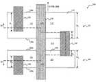
도 1b는 도 1a의 선 1B-1B를 따라 취한 예시적인 집적 회로를 도시한 단면도이다. 주목하는 바와 같이, 도 1a는 집적 회로(100)의 여러 개의 층의 배치도를 간단한 형태로 도시한 도면이다. 도 1b의 단면도를 통해 집적 회로(100)의 추가 특징부를 알 수 있다.FIG. 1B is a cross-sectional view illustrating an exemplary integrated circuit taken along
도 1b를 참조하면, P 타입 트랜지스터(101)와 N 타입 트랜지스터(105)가 기판(103)에 형성될 수 있다. 주목하는 바와 같이, P 타입 트랜지스터(101)와 N 타입 트랜지스터(105)는 절연 구조체(115)에 의해 분리될 수 있다. 일부 실시예에서, 기판(103)은 단원소 반도체 재료, 화합물 반도체 재료, 합금 반도체 재료 또는 다른 적당한 재료 또는 그 조합물을 포함할 수도 있다. 단원소 반도체 재료는 단결정질, 다결정질 또는 무정형 구조의 실리콘 또는 게르마늄을 포함할 수 있다. 화합물 반도체 재료는 탄화 규소, 갈륨 비소, 인화 갈륨, 인화 인듐, 비화 인듐 및 인듐 안티몬을 포함할 수 있다. 합금 반도체 재료는 SiGe, GaAsP, AlInAs, AlGaAs, GaInAs, GaInP 및 GaInAsP를 포함할 수 있다. 일 실시예에서, 합금 반도체 기판은 Si와 Ge 조성이 일 위치에서의 일 비율로부터 다른 위치에서의 다른 비율로 변하는 기울기를 갖는 SiGe 특징을 나타낼 수도 있다. 다른 실시예에서, SiGe 합금이 실리콘 기판 위에 형성된다. 다른 실시예에서, SiGe 기판에 변형 응력이 인가된다. 또한, 반도체 기판은 실리콘 온 인슐레이터(SOI)와 같은 절연체 상의 반도체 또는 박막 트랜지스터(TFT)일 수도 있다. 일부 예에서, 반도체 기판은 도핑 에피텍셜 층 또는 매립 층을 포함할 수도 있다. 다른 예에서, 화합물 반도체 기판은 복층 구조체를 포함할 수도 있으며, 또는 복층 화합물 반도체 구조체를 포함할 수도 있다.Referring to FIG. 1B, a
일부 실시예에서, N 타입 웰(well) 영역(107) 및/또는 P 타입 웰 영역(109)이 각각 P 타입 트랜지스터(101)와 N 타입 트랜지스터(105)용 기판(103)에 임의로 형성될 수 있다. N 타입 웰 영역(107)은 비소(As), 인(P), 다른 5족 성분 또는 그 조합 성분과 같은 도펀트를 구비할 수 있다. P 타입 웰 영역(109)은 붕소(B) 및/또는 다른 3족 성분과 같은 도펀트를 포함할 수 있다.In some embodiments, N
도 1b를 참조하면, P 타입 트랜지스터(101)는 소오스 영역(111)과 드레인 영역(113)을 포함할 수 있다. 일부 실시예에서, 소오스 영역(111)과 드레인 영역(113)은 P 타입 트랜지스터(101)의 채널(도면 부호가 표시되지 않음)에 응력을 인가할 수 있는 구조체(111c 또는 113c)를 각각 포함할 수 있다. 채널의 응력 구조체는 P 타입 트랜지스터(101)의 전기적 특성, 예를 들어, 전류량을 변경하도록 채널 내부의 캐리어의 이동성을 변경할 수 있다. 일부 실시예에서, 소오스 영역(111)과 드레인 영역(113)의 구조체(111c, 113c)는 각각 돌출 소오스 및 돌출 드레인으로 간주할 수 있다. 다른 실시예에서, 각각의 구조체(111c, 113c)는 단일 SiGe 또는 SiXGe1-x 층, 복층 SiGe 또는 SiXGe1-x구조체, 에피텍셜 구조체, 화합물 재료 구조체, P 타입 트랜지스터(101)의 캐리어 이동성을 변경할 수 있는 다른 재료, 또는 그 조합물을 포함할 수 있다.Referring to FIG. 1B, the P-
일부 실시예에서, 소오스 영역(111)과 드레인 영역(113)은 각각, P 타입 저농도 도핑 드레인(LDD)(113a, 113b)을 임의로 포함할 수 있다. P 타입 LDD(113a, 113b)는 각각 N 타입 웰 영역(107)의 도펀트와 정반대 유형의 도펀트를 포함할 수 있다. 다른 실시예에서, 소오스 영역(111)과 드레인 영역(113)은 각각 실리사이드 영역(111b, 113b)을 포함할 수 있다. 실리사이드 영역(111b, 113b)은 니켈 실리사이드(NiSi), 니켈 플라티늄 실리사이드(NiPtSi), 니켈 플라티늄 게르마늄 실리사이드(NiPtGeSi), 니켈 게르마늄 실리사이드(NiGeSi), 이테르븀 실리사이드(YbSi), 플라티늄 실리사이드(PtSi), 이리듐 실리사이드(IrSi), 에르븀 실리사이드(ErSi), 코발트 실리사이드(CoSi), 다른 적당한 재료 또는 그 조합 재료와 같은 적어도 하나의 재료를 포함할 수도 있다.In some embodiments,
도 1b를 다시 참조하면, 게이트 전극부(130a)는 계면 유전 층(117a)을 포함할 수 있다. 계면 유전 층(117a)은 기판(103) 위에 배치될 수 있다. 이러한 계면 유전 층(117a)은 산화 실리콘, 질화 실리콘, 질산화 실리콘, 다른 게이트 유전 재료 또는 그 조합물과 같은 재료를 포함할 수도 있다.Referring back to FIG. 1B, the
일부 실시예에서, 게이트 전극부(130a)는 적어도 하나의 고유전 상수(k)를 갖춘 층과, 적어도 하나의 금속 일 함수(work function) 층을 포함할 수 있는 복층 구조체(131)를 포함할 수 있다. 상기 적어도 하나의 고유전 상수 층은 계면 층(117a) 위에 형성될 수 있다. 고유전 층은 HfO2, HfSiO, HfSiON, HfTaO, HfTiO, HfZrO, 다른 적당한 고유전 재료 또는 그 조합물과 같은 고유전 재료를 포함할 수 있다. 일부 실시예에서, 고유전 재료는 또한, 금속 산화물, 금속 질화물, 금속 규산염, 전이 금속 산화물, 전이 금속 질화물, 전이 금속 규산염, 금속 질산화물, 금속 알루미네이트, 지르코늄 실리케이트, 지르코늄 알루미네이트, 산화 실리콘, 질화 실리콘, 질산화 실리콘, 산화 지르코늄, 산화 티타늄, 산화 알루미늄, 하프늄 디옥사이드 알루미나 합금, 다른 적당한 재료 또는 그 조합물 중에서 선택될 수도 있다.In some embodiments, the
일부 실시예에서, 복층 구조체(131)의 적어도 하나의 금속 일 함수 층은 적어도 하나의 P 금속 일 함수 층과 적어도 하나의 N 금속 일 함수 층을 포함할 수 있다. 다른 실시예에서, 게이트 전극부(130a)의 적어도 하나의 일 금속 일 함수 층은 N 타입 금속 일 함수 층 없이 단지 적어도 하나의 P 타입 금속 일 함수 층을 포함할 수 있다. 일부 실시예에서, P 타입 일 함수 층의 재료는 루테늄, 팔라듐, 플라티늄, 코발트, 니켈, 전도성 금속 산화물과 같은 조성물 및/또는 다른 적당한 재료를 포함할 수 있다. N 타입 금속 재료는 하프늄, 지르코늄, 티타늄, 탄탈륨, 알루미늄, 금속 탄화물(예를 들어, 탄화 하프늄, 탄화 지르코늄, 탄화 티타늄, 탄화 알루미늄), 알루미나이드와 같은 조성물 및/또는 다른 적당한 재료를 포함할 수 있다.In some embodiments, at least one metal work function layer of the
일부 실시예에서, 복층 구조체(131)는 적어도 하나의 확산 배리어를 포함할 수 있다. 적어도 하나의 확산 배리어는 게이트 유전 재료와 일 함수 금속 재료의 사이에 배치될 수 있다. 확산 배리어는 일 함수 금속 재료의 금속 이온이 게이트 유전 재료 내로 확산되는 것을 방지하도록 구성될 수 있다. 확산 배리어는 산화 알루미늄, 알루미늄, 질화 알루미늄, 티타늄, 질화 티타늄(TiN), 탄탈륨, 질화 탄탈륨, 다른 적당한 재료 및/또는 그 조합 재료와 같은 적어도 하나의 재료를 포함할 수도 있다.In some embodiments, the
도 1b를 참조하면, 게이트 전극부(130a)는 전도성 층(135a)을 포함할 수 있다. 전도성 층(135a)은 복층 구조체(131)에 의해 둘러싸이도록 형성될 수 있다. 이러한 전도성 층(135a)은 알루미늄, 구리, Ti, TiN, TaN, Ta, TaC, TaSiN, W, WN, MoN, MoON, RuO2 및/또는 다른 적당한 재료와 같은 적어도 하나의 재료로 형성될 수 있다.Referring to FIG. 1B, the
도 1b를 다시 참조하면, N 타입 트랜지스터(105)는 소오스 영역(121)과 드레인 영역(123)을 포함할 수 있다. 일부 실시예에서, 소오스 영역(121)과 드레인 영역(123)은 각각, N 타입 저농도 도핑 드레인(LDD)(121a, 123a)을 임의로 포함할 수 있다. N 타입 LDD(121a, 123a)는 P 타입 웰 영역(109)의 도펀트와 정반대 유형의 도펀트를 포함할 수 있다. 다른 실시예에서, 소오스 영역(121)과 드레인 영역(123)은 각각 실리사이드 영역(121b, 123b)을 포함할 수 있다. 실리사이드 영역(121b, 123b)은 실리사이드 영역(111b, 113b)의 금속 재료와 동일하거나 유사한 금속 재료를 포함할 수 있다.Referring back to FIG. 1B, the N-
다른 실시예에서, 소오스 영역(121)과 드레인 영역(123)은 각각 응력 구조체(도시하지 않음)를 포함할 수 있다. 응력 구조체는 N 타입 트랜지스터(105)의 채널에서의 캐리어의 이동성을 변경할 수 있다. 일부 실시예에서, 응력 구조체는 각각, 단일 SiC 또는 SixC1-x 층, 복층 SiC 또는 SixC1-x구조체, 에피텍셜 구조체, 화합물 재료 구조체, N 타입 트랜지스터(105)의 캐리어 이동성을 변경할 수 있는 다른 재료 또는 그 조합물을 포함할 수 있다.In other embodiments, the
도 1b를 다시 참조하면, 게이트 전극부(130b)는 계면 유전 층(117b)을 포함할 수 있다. 계면 유전 층(117b)은 기판(103) 위에 배치될 수 있다. 계면 유전 층(117b)은 산화 실리콘, 질화 실리콘, 질산화 실리콘, 다른 게이트 유전 재료 및/또는 그 조합물과 같은 재료를 포함할 수도 있다.Referring back to FIG. 1B, the
일부 실시예에서, 게이트 전극부(130b)는 적어도 하나의 고유전 상수(k) 층과 적어도 하나의 금속 일 함수 층을 포함할 수 있는 복층 구조체(133)를 포함할 수 있다. 적어도 하나의 고유전 층은 계면 층(117b) 위에 형성될 수 있다. 일부 실시예에서, 복층 구조체(133)의 적어도 하나의 고유전 층은 복층 구조체(131)의 고유전 층과 동일하거나 유사할 수 있다.In some embodiments, the
일부 실시예에서, 게이트 전극부(130b)의 적어도 하나의 금속 일 함수 층은 P 타입 금속 일 함수 층 없이 단지 적어도 하나의 N 타입 금속 일 함수 층을 포함할 수 있다. 일부 실시예에서, N 타입 금속 재료는 하프늄, 지르코늄, 티타늄, 탄탈륨, 알루미늄, 금속 탄화물(예를 들어, 탄화 하프늄, 탄화 지르코늄, 탄화 티타늄, 탄화 알루미늄), 알루미나이드와 같은 조성물 및/또는 다른 적당한 재료를 포함할 수 있다.In some embodiments, at least one metal work function layer of
일부 실시예에서, 복층 구조체(133)는 적어도 하나의 확산 배리어를 포함할 수 있다. 적어도 하나의 확산 배리어는 게이트 유전 재료와 일 함수 금속 재료의 사이에 배치될 수 있다. 확산 배리어는 일 함수 금속 재료의 금속 이온이 게이트 유전 재료 내로 확산되는 것을 방지하도록 구성될 수 있다. 확산 배리어는 산화 알루미늄, 알루미늄, 질화 알루미늄, 티타늄, 질화 티타늄(TiN), 탄탈륨, 질화 탄탈륨, 다른 적당한 재료 및/또는 그 조합 재료와 같은 적어도 하나의 재료를 포함할 수도 있다.In some embodiments, the
도 1b를 참조하면, 게이트 전극부(130b)는 전도성 층(135b)을 포함할 수 있다. 전도성 층(135b)은 복층 구조체(133)에 의해 둘러싸이도록 형성될 수 있다. 이러한 전도성 층(135b)은 전도성 층(135a)의 재료와 동일하거나 유사한 적어도 하나의 재료로 형성될 수 있다.Referring to FIG. 1B, the
도 1b를 참조하면, 스페이서(141a, 141b)가 각각, 게이트 전극부(130a, 130b)의 측벽에 임의로 배치될 수 있다. 스페이서(141a, 141b)는 산화 실리콘, 질화 실리콘, 질산화 실리콘, 다른 유전 재료 또는 그 조합 재료와 같은 적어도 하나의 재료로 형성될 수 있다.Referring to FIG. 1B, spacers 141a and 141b may be arbitrarily disposed on sidewalls of the
도 1b를 참조하면, 적어도 하나의 유전 층(151)이 기판(103) 위에 스페이서(104a, 104b)의 둘레에 배치될 수 있다. 적어도 하나의 유전 층(151)은 인 도핑 규산염 유리(PSG), 붕소 도핑 규산염 유리(BSG), 붕소 인 도핑 규산염 유리(BPSG), 비도핑 규산염 유리(USG), 산화 실리콘, 질화 실리콘, 질산화 실리콘, 저유전 상수 재료, 다른 유전 재료 또는 그 조합 재료와 같은 적어도 하나의 재료를 포함할 수 있다.Referring to FIG. 1B, at least one
일부 실시예에서, 적어도 하나의 식각 저지 층(ESL:etch stop layer)(153)이 적어도 하나의 유전 층(151) 위에 배치될 수 있다. 적어도 하나의 ESL(153)은 질화 실리콘, 질산화 실리콘, 실리콘 탄화물, 실리콘 옥시카바이드, 다른 유전 재료 또는 그 조합 재료와 같은 적어도 하나의 재료를 포함할 수 있다.In some embodiments, at least one etch stop layer (ESL) 153 may be disposed over at least one
도 1b를 참조하면, 적어도 하나의 유전 층(153)이 적어도 하나의 ESL(153) 위에 배치될 수 있다. 적어도 하나의 유전 층(153)은 예를 들어, 플라즈마 강화 옥사이드(PEOX), 비도핑 규산염 유리(USG), 인 도핑 규산염 유리(PSG), 붕소 도핑 규산염 유리(BSG), 붕소 인 도핑 규산염 유리(BPSG), 산화 실리콘, 질화 실리콘, 질산화 실리콘, 저유전 상수 재료, 다른 유전 재료 또는 그 조합 재료와 같은 적어도 하나의 재료를 포함할 수 있다.Referring to FIG. 1B, at least one
도 1b에서, 금속 구조체(140, 150, 160)는 유전 층(151, 155)과 ESL(153)을 관통하여 배치될 수 있다. 일부 실시예에서, 금속 구조체(140, 150, 160)는 각각 바닥 영역에 적어도 하나의 배리어 층(도시하지 않음)을 포함할 수 있다. 배리어 층은 산화 알루미늄, 알루미늄, 질화 알루미늄, 티타늄, 질화 티타늄(TiN), 탄탈륨, 질화 탄탈륨, 다른 적당한 재료 및/또는 그 조합물과 같은 적어도 하나의 재료를 포함할 수도 있다. 다른 실시예에서, 금속 구조체(140, 150, 160)는 각각, 알루미늄, 구리, Ti, TiN, TaN, Ta, TaC, TaSiN, W, WN, MoN, MoON, RuO2 및/또는 다른 적당한 재료와 같은 적어도 하나의 재료로 형성될 수 있다.In FIG. 1B, the
일부 실시예에서, 금속 구조체(140, 160)는 소오스 영역(111, 121)과 직접 접촉할 수 있다. 금속 구조체(150)는 드레인 영역(113, 123)과 직접 접촉할 수 있다. 다른 실시예에서, 금속 구조체(140, 160)는 실리사이드 영역(111b, 121b)과 직접 접촉할 수 있다. 금속 구조체(150)는 실리사이드 영역(113b, 123b)과 직접 접촉할 수 있다.In some embodiments, the
일부 실시예에서, 다른 유전 재료, 비아 플러그(via plug), 금속 영역 및/또는 금속 라인(도시하지 않음)이 상호 접속을 위한 게이트 전극부(130a, 130b)의 위에 형성될 수 있다. 유전 층은 산화 실리콘, 질화 실리콘, 질산화 실리콘, 저유전 상수 재료, 초저유전 상수 재료 또는 그 조합물과 같은 재료를 포함할 수도 있다. 비아 플러그, 금속 영역 및/또는 금속 라인은 텅스텐, 알루미늄, 구리, 티타늄, 탄탈륨, 질화 티타늄, 질화 탄탈륨, 니켈 실리사이드, 코발트 실리사이드, 다른 적절한 전도성 재료 및/또는 그 조합물과 같은 재료를 포함할 수 있다. 비아 플러그, 금속 영역 및/또는 금속 라인이 증착, 포토리소그래피 및 에칭 공정 및/또는 그 조합 공정과 같은 다른 적당한 공정에 의해 형성될 수 있다.In some embodiments, other dielectric materials, via plugs, metal regions and / or metal lines (not shown) may be formed over the
도 2a는 예시적인 집적 회로의 예시적인 층 배치도를 개략적으로 도시한 도면이다. 도 1a에서와 동일한 도 2a의 항목은 도 1에서의 도면 부호에 100을 더한 숫자로 지시되어 있다. 도 2a에서, 집적 회로(200)는 각각 소오스 영역(211, 221)과 드레인 영역(213, 223) 중 하나와 직접 접촉하는 복수 개의 금속 구조체, 예를 들어, 금속 구조체(270a 내지 270d)를 포함할 수 있다. 일부 실시예에서, 금속 구조체(270a 내지 270d)는 라우팅 방향으로 개개의 금속 구조체(240, 250, 260)와 적어도 부분적으로 중첩될 수 있다.2A is a schematic illustration of an exemplary layer layout of an exemplary integrated circuit. Items in FIG. 2A that are the same as in FIG. 1A are indicated by numerals plus 100 in FIG. 1. In FIG. 2A, integrated
일부 실시예에서, 각각의 금속 구조체(270a 내지 270d)의 폭은 개개의 금속 구조체(240, 250, 260)의 폭과 실질적으로 동일할 수 있다. 다른 실시예에서, 금속 구조체(270a 내지 270d)는 개개의 금속 구조체(240, 250, 260)보다 넓거나 좁을 수 있다. 일부 실시예에서, 금속 구조체(270a 내지 270d)는 M01 금속 구조체로 간주할 수 있으며, 금속 구조체(240, 250, 260)는 M02 금속 구조체로 간주할 수 있다.In some embodiments, the width of each
일부 실시예에서, 각각의 금속 구조체(270a 내지 270d)는 확산 영역(210)의 일 가장자리(210a)로부터 반대측 가장자리(210b)로 또는 확산 영역(220)의 일 가장자리(220a)로부터 반대측 가장자리(220b)로 연속적으로 연장할 수 있다. 다른 실시예에서, 각각의 금속 구조체(270a 내지 270d)는 확산 영역(210)에 걸쳐 연장할 수 있으며, 또는 확산 영역(210)의 폭(W1')의 대략 5% 이하의 거리만큼 가장자리(210a, 210b)로부터 짧게 연장할 수 있다. 또 다른 실시예에서, 각각의 금속 구조체(270a 내지 270d)는 확산 영역(220)에 걸쳐 연장할 수 있으며, 또는 확산 영역(220)의 폭(W2')의 대략 5% 이하의 거리만큼 가장자리(220a, 220b)로부터 짧게 연장할 수 있다.In some embodiments, each
일부 실시예에서, 금속 구조체(240)와 확산 영역(210)은 라우팅 방향으로 거리(D1')에 걸쳐 중첩될 수 있다. 금속 구조체(250)와 확산 영역(210)은 라우팅 방향으로 거리(D2')에 걸쳐 중첩될 수 있다. 거리(D1')가 거리(D2')보다 길다. 금속 구조체(260)와 확산 영역(220)은 라우팅 방향으로 거리(D3')에 걸쳐 중첩될 수 있다. 금속 구조체(250)와 확산 영역(210)은 라우팅 방향으로 거리(D4')에 걸쳐 중첩될 수 있다. 일부 실시예에서, 거리(D3')가 거리(D4')보다 길다. 다른 실시예에서, 거리(D3')가 거리(D2')보다 길다. 또 다른 실시예에서, 도 1a를 참조하여 전술한 거리(D1, D2, D3 및/또는 D4)가 각각 거리(D1', D2', D3' 및/또는 D4')보다 길 수도 있다.In some embodiments,
일부 실시예에서, 거리(D1')와 거리(D2')의 합이 실질적으로 폭(W1')과 동일할 수 있다. 다른 실시예에서, 거리(D1')와 거리(D2')의 합이 폭(W1')보다 크거나 작을 수 있다. 또 다른 실시예에서, 거리(D3')와 거리(D4')의 합이 실질적으로 폭(W2')과 동일할 수 있다. 또 다른 실시예에서, 거리(D3')와 거리(D4')의 합이 폭(W2')보다 크거나 작을 수 있다.In some embodiments, the sum of the distance D1 ′ and the distance D2 ′ may be substantially equal to the width W1 ′ . In another embodiment, the sum of the distance D1 ′ and the distance D2 ′ may be greater or less than the width W1 ′ . In yet another embodiment, the sum of the distance D3 ' and the distance D4' may be substantially equal to the width W2 ' . In yet another embodiment, the sum of the distance D3 ' and the distance D4' may be greater or less than the width W2 ' .
도 2b는 도 2a의 선 2B-2B를 따라 취한 예시적인 집적 회로를 도시한 단면도이다. 도 2b에서, 금속 구조체(270a 내지 270d)는 각각 소오스 영역(211)과, 드레인 영역(213, 223) 그리고 소오스 영역(221)과 직접 접촉할 수 있다. 금속 구조체(240, 250, 260)는 각각, 금속 구조체(270a 내지 270d)를 통해 소오스 영역(211), 드레인 영역(213, 223) 그리고 소오스 영역(221)과 전기적으로 결합될 수 있다. 일부 실시예에서, 금속 구조체(270a 내지 270d)는 유전 층(251)과 ESL(253)을 관통하여 배치되어, 각각 실리사이드 영역(211b, 213b, 221b, 223b)과 직접 접촉할 수 있다.FIG. 2B is a cross-sectional view illustrating an exemplary integrated circuit taken along
일부 실시예에서, 각각의 금속 구조체(270a 내지 270d)는 바닥 영역에 적어도 하나의 배리어 층(도시하지 않음)을 포함할 수 있다. 배리어 층은 산화 알루미늄, 알루미늄, 질화 알루미늄, 티타늄, 질화 티타늄(TiN), 탄탈륨, 질화 탄탈륨, 다른 적당한 재료 및/또는 그 조합 재료와 같은 적어도 하나의 재료를 포함할 수도 있다. 일부 실시예에서, 각각의 금속 구조체(270a 내지 270d)는 알루미늄, 구리, Ti, TiN, TaN, Ta, TaC, TaSiN, W, WN, MoN, MoON, RuO2, 및/또는 다른 적당한 재료와 같은 적어도 하나의 재료로 형성될 수 있다. 다른 실시예에서, 금속 구조체(270a 내지 270d)는 각각 텅스텐으로 형성될 수 있으며, 금속 구조체(240, 250, 260)는 각각 구리로 형성될 수 있다.In some embodiments, each
일부 실시예에서, 금속 구조체(270a 내지 270d)의 상면은 전도성 층(235a, 235b)의 상면과 실질적으로 동일한 평면일 수 있다. 용어 "실질적으로 동일한 평면"은 금속 구조체(270a 내지 270d)의 상면이 예를 들어, ESL(253)의 두께에 해당하는 거리만큼 전도성 층(235a, 235b)의 상면보다 높게 위치할 수 있음을 의미할 수 있다. 일부 실시예에서, 용어 "실질적으로 동일한 평면"은 에치 백(etch back) 공정 또는 화학 기계적 연마(CMP) 공정으로부터 초래하는 금속 구조체(270a 내지 270d)의 상면 상의 과잉 연마(dishing) 효과로 인해 금속 구조체(270a 내지 270d)의 상면이 ESL(253)의 상면보다 낮게 위치할 수 있음을 의미할 수 있다. 다른 실시예에서, 용어 "실질적으로 동일한 평면"은 에치 백(etch back) 공정 또는 화학 기계적 연마(CMP) 공정으로부터 초래하는 금속 구조체(270a 내지 270d)의 상면 상의 과잉 연마 효과로 인해 금속 구조체(270a 내지 270d)의 상면이 전도성 층(235a, 235b)의 상면보다 낮게 위치할 수 있음을 의미할 수 있다.In some embodiments, the top surfaces of the
도 2a 및 도 2b를 참조하면, 금속 구조체(270a 내지 270d)가 금속 구조체(240, 250, 260)와 개개의 소오스 영역(211), 드레인 영역(213, 223) 및 소오스 영역(221) 사이의 전기 접속부용으로 전개될 수 있음을 알 수 있다. 금속 구조체(270a 내지 270d)는 실질적으로 라우팅 방향으로 개개의 확산 영역(210, 220)을 덮을 수 있다. 소오스 영역과 드레인 영역에 대한 금속 구조체(270a 내지 270d)의 저항은 바람직하게 감소될 수 있다. 일부 실시예에서, 전기 접속부용으로 전개될 수 있는 금속 구조체(240, 250, 260)의 중첩 거리(D1' 내지 D4')가 감소될 수 있다. 또한, 금속 구조체(270a 내지 270d)의 상면은 전도성 층(235a, 235b)의 상면과 실질적으로 동일한 평면일 수 있음을 알 수 있다. 금속 구조체(270a 및 270b) 사이 및 금속 구조체(270c 및 270d) 사이의 기생 용량은 낮다.2A and 2B,
도 3은 집적 회로를 형성하기 위한 예시적인 일 방법을 도시한 순서도이다. 도 4a 내지 도 4e는 도 2a의 선 2B-2B를 따라 취한 집적 회로(200)를 형성하기 위한 다른 예시적인 방법을 개략적으로 도시한 단면도이다. 도 3에서, 집적 회로를 형성하기 위한 방법(300)은 기판 상의 제 1 확산 영역과 제 2 확산 영역을 형성하는 단계(공정(310))를 포함할 수 있다.3 is a flow chart illustrating one exemplary method for forming an integrated circuit. 4A-4E are schematic cross-sectional views of another exemplary method for forming the
일부 실시예에서, 공정(310)에서는 도 2a 및 도 4a에 도시된 바와 같이 기판(203) 상에 확산 영역(210, 220)이 형성될 수 있다. 일부 실시예에서, 공정(310)은 확산 영역(220)으로부터 확산 영역(210)을 분리하는 절연 구조체(215)를 형성하는 단계를 포함할 수 있다. 일부 실시예에서, 절연 구조체(215)의 형성은 포토리소그래피 공정에 의해 반도체 기판(203)을 패터닝하는 단계와, 기판에 트렌치를 에칭(예를 들어, 건식 에칭, 습식 에칭 및/또는 플라즈마 에칭 공정을 사용)하는 단계, 그리고 유전 재료로 트렌치를 충전(예를 들어, 화학 증착 공정을 사용)하는 단계를 포함할 수도 있다. 일부 실시예에서, 절연 구조체(215)는 산화 실리콘 또는 질화 실리콘으로 충전된 열 산화 라이너 층과 같은 복층 구조체를 포함할 수도 있다. 일부 실시예에서, 공정(310)은 STI 공정 또는 LOCOS 공정으로 간주할 수 있다.In some embodiments, in process 310,
도 4a를 참조하면, 일부 실시예에서, N 타입 웰 영역(207) 및/또는 P 타입 웰 영역(209)이 각각 확산 영역(201)과 확산 영역(205)에 임의로 형성될 수 있다. N 타입 웰 영역(207) 및/또는 P 타입 웰 영역(209)은, 예를 들어, 포토리소그래피 공정 및 이온 이식 공정에 의해 형성될 수 있다. 일부 실시예에서, N 타입 웰 영역(207) 및/또는 P 타입 웰 영역(209)의 도펀트를 활성화하기 위하여 열처리 공정 및/또는 급속 열처리 공정(RTP)이 수행될 수 있다.Referring to FIG. 4A, in some embodiments, an N
도 3을 참조하면, 방법(300)은 제 1 확산 영역에 제 1 유형의 트랜지스터를 형성하기 위해 드레인 영역과 소오스 영역을 형성하는 단계(공정(320))를 포함할 수 있다. 도 4a에 도시된 바와 같은 P 타입 트랜지스터(201)를 형성하는 일부 실시예에서, 공정(320)에서는 소오스 영역(211)과 드레인 영역(213)을 형성할 수 있다. 일부 실시예에서, 소오스 영역(211)과 드레인 영역(213)은 각각, 예를 들어, 포토리소그래피 및 이온 이식 공정에 의해 형성될 수 있는 P 타입 고농도 도핑 영역을 포함할 수 있다.Referring to FIG. 3,
다른 실시예에서, 공정(320)은 소오스 영역(211)과 드레인 영역(213)에 각각 구조체(211c, 213c)를 형성하는 단계를 포함할 수 있다. 구조체(211c, 213c)는 P 타입 트랜지스터(201)의 채널에 응력을 인가할 수 있다. 일부 실시예에서, 구조체(211c, 213c)는 에피텍셜 공정, 감압 화학 증착(RPCVD) 공정, 분자 빔 에피택시(MBE) 공정, 화학 증착(CVD) 공정, 금속 유기 화학 증착(MOCVD) 공정, 원자 층 증착(ALD) 공정, 복층 에피택셜 공정 또는 그 조합 방법에 의해 형성될 수 있다.In another embodiment, the
일부 실시예에서, 공정(320)은 임의로, 스페이서(241a)의 아래에 P 타입 LDD(211a, 213a)를 형성하는 단계를 포함할 수 있다. P 타입 LDD(211a, 213a)는, 예를 들어, 경사각 이온 이식 공정에 의해 형성될 수 있다. 일부 실시예에서, 게이트 전극부를 형성하는 공정(340)에 앞서, 실리사이드 영역이 기판(211c, 213c) 상에 형성될 수 있다. 이러한 공정을 실리사이드 전기 형성 공정으로 간주할 수 있다. 다른 실시예에서, 공정(320)은 도 4c를 참조하여 아래에 설명되는 실리사이드 영역(211b, 211c)을 형성하는 단계를 포함할 수 있다. 다른 일부 실시예에서, 소오스 영역(211)과 드레인 영역(213)의 도펀트를 활성화하기 위하여 열처리 공정 및/또는 급속 열처리 공정(RTP)이 임의로 수행될 수 있다.In some embodiments,
도 3을 참조하면, 방법(300)은 제 2 확산 영역에 제 2 유형의 트랜지스터를 형성하기 위해 드레인 영역과 소오스 영역을 형성하는 단계[공정(330)]를 포함할 수 있다. 도 4a에 도시된 바와 같은 N 타입 트랜지스터(205)를 형성하는 일부 실시예에서, 공정(330)에서는 소오스 영역(221)과 드레인 영역(223)을 형성할 수 있다. 일부 실시예에서, 소오스 영역(221)과 드레인 영역(223)은 각각, 예를 들어, 포토리소그래피 및 이온 이식 공정에 의해 형성될 수 있는 N 타입 고농도 도핑 영역을 포함할 수 있다.Referring to FIG. 3,
다른 실시예에서, 공정(330)은 소오스 영역(211)과 드레인 영역(213)에 각각 응력 구조체(도시하지 않음)를 형성하는 단계를 포함할 수 있다. 상기 응력 구조체는 구조체(211c, 213c)에 의해 제공되는 응력과 반대 방향으로 N 타입 트랜지스터(205)의 채널에 응력을 인가할 수 있다. 이러한 응력 구조체는 에피텍셜 공정, 감압 화학 증착(RPCVD) 공정, 분자 빔 에피택시(MBE) 공정, 화학 증착(CVD) 공정, 금속 유기 화학 증착(MOCVD) 공정, 원자 층 증착(ALD) 공정, 복층 에피택셜 공정 또는 그 조합 방법에 의해 형성될 수 있다.In another embodiment,
일부 실시예에서, 공정(330)은 임의로, 스페이서(241b)의 아래에 N 타입 LDD(221a, 223a)를 형성하는 단계를 포함할 수 있다. N 타입 LDD(221a, 223a)는, 예를 들어, 경사각 이온 이식 공정에 의해 형성될 수 있다. 일부 실시예에서, 게이트 전극부를 형성하는 공정(340)에 앞서, 실리사이드 영역이 소오스 영역(211)과 드레인 영역(213)에 형성될 수 있다. 이러한 공정을 실리사이드 전기 형성 공정으로 간주할 수 있다. 다른 실시예에서, 공정(330)은 도 4c를 참조하여 아래에 설명되는 실리사이드 영역(221b, 221c)을 형성하는 단계를 포함할 수 있다. 다른 일부 실시예에서, 소오스 영역(221)과 드레인 영역(223)의 도펀트를 활성화하기 위하여 열처리 공정 및/또는 급속 열처리 공정(RTP)이 임의로 수행될 수 있다. 도 3을 참조하여 전술한 공정(320, 330)의 순서는 바뀔 수 있음에 주목하여야 한다. 예를 들어, 공정(330)이 공정(320)보다 먼저 수행될 수 있다. 또한, 각각의 공정(320, 330)의 공정 단계 및/또는 그 순서가 변경 및/또는 뒤바뀔 수 있음에 주목하여야 한다. 본 출원의 영역이 전술한 바로만 제한되는 것은 아니다.In some embodiments,
도 3을 참조하면, 방법(300)은 제 1 확산 영역과 제 2 확산 영역을 가로질러 연속적으로 연장하는 게이트 전극을 형성하는 단계를 포함할 수 있다(공정(340)). 일부 실시예에서, 방법은 도 2a에 도시된 바와 같은 게이트 전극(230)을 형성하는 단계를 포함할 수 있다.Referring to FIG. 3, the
게이트 전극(230)은 게이트 전기 형성 공정 또는 게이트 후기 형성 공정에 의해 형성될 수 있다. 게이트 후기 형성 공정을 이용하는 일부 실시예에서, 공정(340)은 도 4a에 도시된 바와 같이 기판(203) 위에 더미 게이트 전극(232a, 232b)을 형성하는 단계를 포함할 수 있다. 더미 게이트 전극(232a, 232b)은 폴리실리콘, 무정형 실리콘, 산화 실리콘, 질화 실리콘, 유전 층(251) 및/또는 스페이서(241a, 241b)와 실질적으로 식각률이 다른 재료와 같은 적어도 하나의 재료로 형성될 수 있다. 일부 실시예에서, 더미 게이트 전극(232a, 232b)은 CVD 공정에 의해 형성될 수 있다.The
공정(340)은, 예를 들어, 습식 에칭 공정, 건식 에칭 공정 또는 그 조합 방법에 의해 더미 게이트 전극(232a, 232b)을 제거하는 단계를 포함할 수 있다. 더미 게이트 전극(232a, 232b)을 제거한 후, 공정(340)은 기판(203) 위에 게이트 전극부(230a, 230b)를 형성하는 단계를 포함할 수 있다. 게이트 전극부(230a, 230b)는 각각 복층 구조체(231, 233)와 전도성 층(235a, 235b)을 포함할 수 있다. 복층 구조체(231, 233)는, 예를 들어, ALD 공정, CVD 공정, 물리적 증착(PVD) 공정, 감압 CVD(RPCVD) 공정, PECVD 공정, MOCVD 공정 또는 그 조합 방법과 같은 적당한 공정에 의해 형성될 수 있다. 전도성 층(235a, 235b)은, 예를 들어, ALD 공정, CVD 공정, 물리적 증착(PVD) 공정, 감압 CVD(RPCVD) 공정, PECVD 공정, MOCVD 공정, 도금 공정, 스퍼터링 공정, 또는 그 조합 방법과 같은 적당한 공정에 의해 형성될 수 있다. 게이트 전극부(230a, 230b)의 형성 후, ESL(253)이, 예를 들어, CVD 공정에 의해 게이트 전극부(230a, 230b) 위에 형성될 수 있다.The
도 3을 다시 참조하면, 방법(300)은 제 1 금속 구조체와, 제 2 금속 구조체 및 제 3 금속 구조체를 형성하는 단계(공정(350))를 포함할 수 있다. 제 1 금속 구조체는 제 1 소오스 영역과 전기적으로 결합될 수 있으며, 제 2 금속 구조체는 제 1 드레인 영역 및 제 2 드레인 영역과 전기적으로 결합될 수 있고, 제 3 금속 구조체는 제 2 소오스 영역과 전기적으로 결합될 수 있다.Referring again to FIG. 3, the
도 1b에 도시된 단면도와 유사한 방식으로 금속 구조체를 형성하는 일부 실시예에서, 유전 층(155)이 ESL(153)의 위에 형성될 수 있다. 금속 구조체(140, 150, 160)가 유전 층(151, 155) 및 ESL(153)을 관통하여 형성될 수 있으므로, 금속 구조체(140, 150, 160)는 개개의 소오스 및 드레인 영역(111, 113, 121, 123)과 직접 접촉할 수 있다.In some embodiments forming a metal structure in a manner similar to the cross-sectional view shown in FIG. 1B, a
도 2a 및 도 2b에 도시된 구조체와 유사한 방식으로 금속 구조체를 형성하는 일부 실시예에서, 방법(300)은 개개의 금속 구조체(240, 250, 260)와 전기적으로 결합되는 금속 구조체(270a, 270b)를 형성하는 단계를 추가로 포함할 수 있다. 일부 실시예에서, 방법(300)은 유전 층(251)과 ESL(253)을 통하여 개구(271a, 271c)를 형성하는 단계를 포함할 수 있다. 도 4c에 도시된 바와 같이, 개구(271a 내지 271c)에 의해 개개의 소오스 및 드레인 영역(211, 213, 221, 223)이 적어도 부분적으로 노출될 수 있다.In some embodiments of forming a metal structure in a manner similar to the structure shown in FIGS. 2A and 2B, the
일부 실시예에서, 개구(271a 내지 271c)를 형성한 후, 실리사이드 영역(211b, 213b, 221b, 223b)이 개개의 소오스 및 드레인 영역(211, 213, 221, 223)에 형성될 수 있다. 주목하는 바와 같이, 복층 구조체(231, 233)의 고유전 상수 층과 계면 층(217a, 217b)의 형성 후 도 4c에 도시된 실리사이드 영역(211b, 213b, 221b, 223b)이 형성된다. 실리사이드 영역(211b, 213b, 221b, 223b)은 복층 구조체(231, 233)의 고유전 상수 층과 계면 층(217a, 217b)을 형성하는 열처리 주기와 무관하다. 일부 실시예에서, 전술한 바와 같이 실리사이드 영역(211b, 213b, 221b, 223b)을 형성하는 공정을 실리사이드 후기 형성 공정으로 간주할 수 있다.In some embodiments, after forming the
도 4d를 참조하면, 방법(300)은 개개의 소오스 및 드레인 영역(211, 213, 221, 223)과 직접 접촉하는 금속 구조체(270a 내지 270d)를 형성하는 단계를 포함할 수 있다. 금속 구조체(270a 내지 270d)는, 예를 들어, PVD 공정, CVD 공정, ALD 공정, 스퍼터링 공정, 도금 공정, 다른 적당한 방법 또는 그 조합 방법을 사용한 증착에 의해 형성될 수 있다.Referring to FIG. 4D, the
도 4e를 참조하면, 공정(350)(도 3에 도시됨)은 개개의 금속 구조체(270a 내지 270d)와 전기적으로 결합되는 금속 구조체(240, 250, 260)를 형성하는 단계를 포함할 수 있다. 일부 실시예에서, 공정(350)은 유전 층(255)을 관통하는 개구(도면 부호가 표시되지 않음)를 형성하는 단계를 포함할 수 있다. 상기 개구는 개개의 금속 구조체(270a 내지 270d)를 적어도 부분적으로 노출시킬 수 있다. 이후, 금속 구조체(240, 250, 260)가 개구의 내부에 형성되어, 개개의 금속 구조체(270a 내지 270d)와 전기적으로 결합될 수 있다. 일부 실시예에서, 금속 구조체(240, 250, 260)는, 예를 들어, PVD 공정, CVD 공정, ALD 공정, 스퍼터링 공정, 플레이팅 공정, 다른 적당한 방법 및/또는 그 조합 방법을 사용한 증착에 의해 형성될 수 있다.Referring to FIG. 4E, process 350 (shown in FIG. 3) may include forming
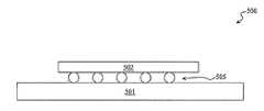
도 5는 기판 보드 상에 배치된 예시적인 집적 회로를 포함하는 시스템을 개략적으로 도시한 도면이다. 도 5에서, 시스템(500)은 기판 보드(501) 위에 배치되는 집적 회로(502)를 포함할 수 있다. 기판 보드(501)는, 일부 실시예에서, 인쇄 회로 보드(PCB), 인쇄 배선 보드 및/또는 직접 회로를 지탱할 수 있는 다른 캐리어를 포함할 수 있다. 집적 회로(502)는 도 1a 및 도 1b 그리고 도 2a 및 도 2b를 참조하여 전술한 집적 회로(100 또는 200)와 유사할 수 있다. 집적 회로(502)는 기판 보드(501)와 전기적으로 결합될 수 있다. 일부 실시예에서, 집적 회로(502)는 범프(bump:505)를 통해 기판 보드(501)와 전기적으로 결합될 수 있다. 다른 실시예에서, 집적 회로(502)는 와이어 접합(도시하지 않음)을 통해 기판 보드(501)와 전기적으로 결합될 수 있다. 일부 실시예에서, 시스템(500)은 컴퓨터, 무선 통신 장치, 컴퓨터 관련 주변 구성, 오락기 등과 같은 전자 시스템의 일부를 구성할 수 있다.5 is a schematic illustration of a system including an exemplary integrated circuit disposed on a substrate board. In FIG. 5,
일부 실시예에서, 집적 회로(502)를 포함하는 시스템(500)은 이른바, 시스템 온 칩(SOC) 또는 시스템 온 집적 회로(SOIC) 소자라 불리우는 하나의 IC 형태로 전체 시스템이 제공될 수 있다. SOC/SOIC 소자는, 예를 들어, 휴대폰, 개인용 정보 단말기(PDA), 디지털 VCR, 디지털 캠코더, 디지털 카메라, MP3 플레이어 등을 단일 집적 회로로 실시하기 위해 필요한 모든 회로 소자를 제공할 수도 있다.In some embodiments,
도 6은 예시적인 집적 회로의 예시적인 층 배치도를 개략적으로 도시한 도면이다. 도 2a에서와 동일한 도 6의 항목은 도 2a에서와 동일한 도면 부호에 100을 더한 숫자로 지시되어 있다. 도 6에서, 집적 회로(600)는 각각 상이한 유형의 트랜지스터(601, 605)용으로 구성되며 서로 분리되어 있는 확산 영역(610, 620)을 포함한다. 예를 들어, 확산 영역(610)은 P 타입 트랜지스터용으로 구성되며 확산 영역(620)은 N 타입 트랜지스터용으로 구성된다. 트랜지스터(601)는 확산 영역(610)에 소오스 영역(611)과 드레인 영역(613)을 포함한다. 트랜지스터(605)는 확산 영역(620)에 소오스 영역(621)과 드레인 영역(623)을 포함한다.6 is a schematic illustration of an exemplary layer layout of an exemplary integrated circuit. The items in FIG. 6 that are the same as in FIG. 2A are indicated by the same reference numerals as in FIG. 2A plus 100. In FIG. 6, integrated
도 6을 참조하면, 게이트 전극(630)을 포함하는 집적 회로(600)는 라우팅 방향으로 확산 영역(610, 620)을 가로질러 연속적으로 연장한다. 일부 실시예에서, 집적 회로(600)는 복수 개의 금속 구조체, 예를 들어, 각각 소오스 영역(611, 621) 및 드레인 영역(613, 623)과 직접 접촉하는 금속 구조체(670a 내지 670d)를 포함한다. 집적 회로(600)는 금속 구조체(670a, 670b, 670d, 670c)와 각각 전기적으로 결합되며 이들 금속 구조체 위에 배치되는 금속 구조체(640, 650, 660)를 포함할 수 있다. 일부 실시예에서, 금속 구조체(650)는 금속 구조체(670b)로부터 금속 구조체(670d)로 연속적으로 연장한다.Referring to FIG. 6, the
일부 실시예에서, 금속 구조체(670b)의 폭(WM1)은 금속 구조체(650)의 폭(WM2)과 실질적으로 동일하거나 보다 크다. 다른 실시예에서, 폭(WM1) 대 폭(WM2)의 비는 대략 1:1 내지 대략 2:1의 범위일 수 있다. 또 다른 실시예에서, 폭(WM1) 대 폭(WM2)의 비는 대략 1.3:1 내지 대략 1.6:1의 범위일 수 있다.In some embodiments, the width WM1 of the
일부 실시예에서, 금속 구조체(670d)의 폭(WM3)은 금속 구조체(650)의 폭(WM2)과 실질적으로 동일하거나 보다 크다. 다른 실시예에서, 폭(WM3) 대 폭(WM2)의 비는 대략 1:1 내지 대략 2:1의 범위일 수 있다. 또 다른 실시예에서, 폭(WM1) 대 폭(WM2)의 비는 대략 1.3:1 내지 대략 1.6:1의 범위일 수 있다.In some embodiments, the width WM3 of the
일부 실시예에서, 금속 구조체(670a)의 폭(WM4)은 금속 구조체(660)의 폭(WM5)과 실질적으로 동일하거나 보다 크다. 다른 실시예에서, 폭(WM4) 대 폭(WM5)의 비는 대략 1:1 내지 대략 2:1의 범위일 수 있다. 또 다른 실시예에서, 폭(WM4) 대 폭(WM5)의 비는 대략 1.3:1 내지 대략 1.6:1의 범위일 수 있다.In some embodiments, the width WM4 of the
일부 실시예에서, 금속 구조체(670c)의 폭(WM6)은 금속 구조체(660)의 폭(WM7)과 실질적으로 동일하거나 보다 크다. 다른 실시예에서, 폭(WM6) 대 폭(WM7)의 비는 대략 1:1 내지 대략 2:1의 범위일 수 있다. 또 다른 실시예에서, 폭(WM6) 대 폭(WM7)의 비는 대략 1.3:1 내지 대략 1.6:1의 범위일 수 있다.In some embodiments, the width WM6 of the
적어도 하나의 폭(WM1, WM3, WM4, 또는 WM6)이 폭((WM2, WM5, WM76)과 실질적으로 동일하거나 보다 크다는 점에 주목하여야 한다. 일부 실시예에서, 금속 구조체(670a 내지 670d) 중 하나만이 보다 넓게 형성되며 집적 회로(600)에 적용된다. 다른 실시예에서, 금속 구조체(670a 내지 670d) 중 두 개 이상이 보다 넓으며 집적 회로(600)에 적용된다. 또 다른 실시예에서, 모든 금속 구조체(670a 내지 670d)가 개개의 금속 구조체(640, 650, 660)보다 넓다.It should be noted that at least one width WM1 , WM3 , WM4 , or WM6 is substantially the same as or greater than the width WM2 , WM5 , WM76 . In some embodiments, the metal Only one of the
주목하는 바와 같이, 금속 구조체(640, 650, 660 및/또는 670a 내지 670d)의 폭 및/또는 길이를 조절함으로써 집적 회로(600)의 접촉 저항 및/또는 기생 용량을 변경할 수 있다. 접촉 저항 및/또는 기생 용량의 변경은 집적 회로(600)의 작동 속도에 영향을 미칠 수도 있다. 예를 들어, 각각의 금속 구조체(640, 650, 660)의 폭은 각각의 시료(I 내지 V)의 경우에 대략 20 nm의 값으로 고정된다. 시료(I 내지 V)의 각각의 금속 구조체(670a 내지 670d)의 폭은 대략 26nm, 30nm, 32nm, 34nm 및 38nm이다. 이에 따라, 금속 구조체(670a 내지 670d)와 개개의 금속 구조체(640, 650, 660)의 폭 비는 각각, 시료(I 내지 V)의 경우에 1.3:1, 1.5:1, 1.6:1, 1.7:1 및 1.9:1이다. 전술한 금속 구조체(670a 내지 670d)의 크기는 단지 예시적으로 주어진 것임에 주목하여야 한다. 일부 실시예에서, 금속 구조체(670a 내지 670d)의 크기는 적용된 기술적 중심점에 따라 크기가 축소 또는 확대될 수 있다. 적용 범위가 이로만 제한되는 것은 아니다.As noted, the contact resistance and / or parasitic capacitance of the
표 2에는 전술한 바와 같은 폭 비의 변경에 따라 집적 회로의 작동 속도와 접촉 저항 그리고 기생 용량을 포함하는 시뮬레이션 결과가 기재되어 있다.Table 2 lists the simulation results including the operating speed, contact resistance and parasitic capacitance of the integrated circuit as the width ratio is changed as described above.
본 출원인은 금속 구조체(640, 650, 660 및/또는 670a 내지 670d)간의 폭 비 변경이 집적 회로의 작동 속도와 관련하여 예상하지 못한 개선을 달성할 수 있음을 발견하였다. 표 2에 나타내어진 바와 같이, 폭 비가 1.3:1인 시료(I)의 집적 회로가 베이스로서 사용되고 있다. 금속 구조체(640, 650, 660)의 폭이 동일한 경우 시료(I 내지 V)의 기생 용량이 동일함을 알 수 있다. 또한, 시료(I 내지 V)의 금속 구조체(670a 내지 670d)의 폭의 증가로 인해 접촉 저항이 점차적으로 감소함을 알 수 있다. 접촉 저항 증가에 의해, 집적 회로의 작동 속도가 금속 구조체(670a 내지 670d)의 폭이 증가함에 따라 증가한다.Applicants have found that changing the width ratio between
집적 회로(600)가 도 3을 참조하여 전술한 방법(300)과 동일하거나 실질적으로 유사한 방법 및/또는 도 4a 내지 도 4e를 참조하여 전술한 공정 단계에 의해 형성될 수 있음에 주목하여야 한다. 방법의 상세한 설명은 반복 기재되지 않는다. 또한, 집적 회로(600)가 도 5를 참조하여 전술한 시스템(500)에 적용될 수 있음에 주목하여야 한다.It should be noted that the
본 용례의 실시예에 있어서, 집적 회로는 제 1 유형 트랜지스터를 위한 제 1 확산 영역을 포함한다. 제 1 유형 트랜지스터는 제 1 드레인 영역과 제 1 소오스 영역을 포함한다. 제 2 유형 트랜지스터를 위한 제 2 확산 영역은 제 1 확산 영역으로부터 분리된다. 제 2 유형 트랜지스터는 제 2 드레인 영역과 제 2 소오스 영역을 포함한다. 게이트 전극은 라우팅 방향으로 제 1 확산 영역과 제 2 확산 영역을 가로질러 연속적으로 연장한다. 제 1 금속 구조체는 제 1 소오스 영역과 전기적으로 결합된다. 제 2 금속 구조체는 제 2 드레인 영역과 전기적으로 결합된다. 제 3 금속 구조체는 제 1 및 제 2 금속 구조체 위에 배치되어 이들 금속 구조체와 전기적으로 결합된다. 제 1 금속 구조체의 폭은 제 3 금속 구조체의 폭과 실질적으로 동일하거나 보다 크다.In an embodiment of this application, an integrated circuit includes a first diffusion region for a first type transistor. The first type transistor includes a first drain region and a first source region. The second diffusion region for the second type transistor is separated from the first diffusion region. The second type transistor includes a second drain region and a second source region. The gate electrode extends continuously across the first diffusion region and the second diffusion region in the routing direction. The first metal structure is electrically coupled with the first source region. The second metal structure is electrically coupled with the second drain region. The third metal structures are disposed over and electrically coupled to the first and second metal structures. The width of the first metal structure is substantially equal to or greater than the width of the third metal structure.
당업자라면 다수의 실시예의 전술한 개략적인 특징으로부터 본 발명의 태양을 보다 잘 이해될 수 있을 것이다. 또한, 당 업자라면 본 발명을 사용하여 전술한 실시예와 동일한 장점을 달성하며 및/또는 동일한 목적을 수행하기 위한 다른 공정 및 구조체를 용이하게 설계 또는 수정할 수도 있음을 알 수 있을 것이다. 당업자라면 또한, 이러한 등가의 구성이 본 발명의 정신 및 영역으로부터 벗어나지 않으며 본 발명의 정신 및 영역으로부터 벗어남이 없이 다양한 변경, 대안 및 변형이 이루어질 수도 있음을 이해할 수 있을 것이다.Those skilled in the art will be able to better understand aspects of the present invention from the foregoing schematic features of a number of embodiments. It will also be appreciated by those skilled in the art that the present invention may be readily designed or modified to achieve the same advantages as the embodiments described above and / or to perform the same purposes. Those skilled in the art will also appreciate that such equivalent constructions do not depart from the spirit and scope of the present invention and that various changes, alternatives, and modifications may be made without departing from the spirit and scope of the present invention.
100 : 집적 회로 101 : P 타입 트랜지스터
105 : N 타입 트랜지스터 110, 120 : 확산 영역
111 : 소오스 영역 113 : 드레인 영역
115 : 절연 구조체 130 : 게이트 전극100: integrated circuit 101: P type transistor
105:
111: source region 113: drain region
115: insulating structure 130: gate electrode
Claims (10)
Translated fromKorean제 1 유형 트랜지스터를 위한 제 1 확산 영역으로서, 상기 제 1 유형 트랜지스터는 상기 제 1 확산 영역 내에 제 1 드레인 영역과 제 1 소오스 영역을 포함하는 것인 상기 제 1 확산 영역;
상기 제 1 확산 영역으로부터 분리되어 있는, 제 2 유형 트랜지스터를 위한 제 2 확산 영역으로서, 상기 제 2 유형 트랜지스터는 상기 제 2 확산 영역 내에 제 2 드레인 영역과 제 2 소오스 영역을 포함하는 것인 상기 제 2 확산 영역;
라우팅 방향으로 상기 제 1 확산 영역과 상기 제 2 확산 영역을 가로질러 연속적으로 연장하는 게이트 전극;
상기 제 1 드레인 영역과 전기적으로 결합되는 제 1 금속 구조체;
상기 제 2 드레인 영역과 전기적으로 결합되는 제 2 금속 구조체;
상기 제 1 금속 구조체 및 상기 제 2 금속 구조체 위에 배치되며 이들 금속 구조체와 전기적으로 결합되는 제 3 금속 구조체 - 상기 제 1 금속 구조체의 폭은 상기 제 3 금속 구조체의 폭보다 큼 - ;
상기 제 1 소오스 영역과 전기적으로 결합되는 제 4 금속 구조체;
상기 제 4 금속 구조체 위에 배치되며 상기 제 4 금속 구조체와 전기적으로 결합되는 제 5 금속 구조체 - 상기 제 5 금속 구조체와 상기 제 1 확산 영역은 상기 라우팅 방향으로 제 1 거리만큼 중첩되고, 상기 제 3 금속 구조체와 상기 제 1 확산 영역은 상기 라우팅 방향으로 제 2 거리만큼 중첩되며, 상기 제 1 거리는 상기 제 2 거리보다 긴 것임 - ;
상기 제 2 소오스 영역과 전기적으로 결합되는 제 6 금속 구조체; 및
상기 제 6 금속 구조체 위에 배치되며 상기 제 6 금속 구조체와 전기적으로 결합되는 제 7 금속 구조체 - 상기 제 7 금속 구조체와 상기 제 2 확산 영역은 상기 라우팅 방향으로 제 3 거리만큼 중첩되며, 상기 제 3 금속 구조체와 상기 제 2 확산 영역은 상기 라우팅 방향으로 제 4 거리만큼 중첩되고, 상기 제 3 거리는 제 4 거리보다 긴 것임 -
를 포함하는, 집적 회로.As an integrated circuit,
A first diffusion region for a first type transistor, wherein the first type transistor comprises a first drain region and a first source region in the first diffusion region;
A second diffusion region for a second type transistor, separate from the first diffusion region, wherein the second type transistor includes a second drain region and a second source region in the second diffusion region; 2 diffusion regions;
A gate electrode continuously extending across said first diffusion region and said second diffusion region in a routing direction;
A first metal structure electrically coupled with the first drain region;
A second metal structure electrically coupled with the second drain region;
A third metal structure disposed over and electrically coupled to the first metal structure and the second metal structure, the width of the first metal structure being greater than the width of the third metal structure;
A fourth metal structure electrically coupled with the first source region;
A fifth metal structure disposed over the fourth metal structure and electrically coupled to the fourth metal structure, wherein the fifth metal structure and the first diffusion region overlap each other by the first distance in the routing direction, and the third metal The structure and the first diffusion region overlap in the routing direction by a second distance, the first distance being longer than the second distance;
A sixth metal structure electrically coupled with the second source region; And
A seventh metal structure disposed on the sixth metal structure and electrically coupled to the sixth metal structure, wherein the seventh metal structure and the second diffusion region overlap each other by a third distance in the routing direction, and the third metal The structure and the second diffusion region overlap a fourth distance in the routing direction, the third distance being longer than a fourth distance −
≪ / RTI >
제 1 유형 트랜지스터를 위한 제 1 확산 영역으로서, 상기 제 1 유형 트랜지스터는 상기 제 1 확산 영역 내에 제 1 드레인 영역과 제 1 소오스 영역을 포함하는 것인 상기 제 1 확산 영역;
상기 제 1 확산 영역으로부터 분리되어 있는, 제 2 유형 트랜지스터를 위한 제 2 확산 영역으로서, 상기 제 2 유형 트랜지스터는 상기 제 2 확산 영역 내에 제 2 드레인 영역과 제 2 소오스 영역을 포함하는 것인 상기 제 2 확산 영역;
라우팅 방향으로 상기 제 1 확산 영역과 상기 제 2 확산 영역을 가로질러 연속적으로 연장하는 게이트 전극;
상기 제 1 드레인 영역과 전기적으로 결합되는 제 1 금속 구조체;
상기 제 2 드레인 영역과 전기적으로 결합되는 제 2 금속 구조체;
상기 제 1 금속 구조체 및 상기 제 2 금속 구조체 위에 배치되며 이들 금속 구조체와 전기적으로 결합되는 제 3 금속 구조체로서, 상기 제 1 금속 구조체의 폭 대 상기 제 3 금속 구조체의 폭의 비가 1.3:1 내지 1.6:1의 범위인 것인 상기 제 3 금속 구조체;
상기 제 1 소오스 영역과 전기적으로 결합되는 제 4 금속 구조체;
상기 제 4 금속 구조체 위에 배치되며 상기 제 4 금속 구조체와 전기적으로 결합되는 제 5 금속 구조체 - 상기 제 5 금속 구조체와 상기 제 1 확산 영역은 상기 라우팅 방향으로 제 1 거리만큼 중첩되고, 상기 제 3 금속 구조체와 상기 제 1 확산 영역은 상기 라우팅 방향으로 제 2 거리만큼 중첩되며, 상기 제 1 거리는 상기 제 2 거리보다 긴 것임 -
상기 제 2 소오스 영역과 전기적으로 결합되는 제 6 금속 구조체; 및
상기 제 6 금속 구조체 위에 배치되며 상기 제 6 금속 구조체와 전기적으로 결합되는 제 7 금속 구조체 - 상기 제 7 금속 구조체와 상기 제 2 확산 영역은 상기 라우팅 방향으로 제 3 거리만큼 중첩되며, 상기 제 3 금속 구조체와 상기 제 2 확산 영역은 상기 라우팅 방향으로 제 4 거리만큼 중첩되고, 상기 제 3 거리는 상기 제 4 거리보다 긴 것임 -
를 포함하는, 집적 회로.As an integrated circuit,
A first diffusion region for a first type transistor, wherein the first type transistor comprises a first drain region and a first source region in the first diffusion region;
A second diffusion region for a second type transistor, separate from the first diffusion region, wherein the second type transistor includes a second drain region and a second source region in the second diffusion region; 2 diffusion regions;
A gate electrode continuously extending across said first diffusion region and said second diffusion region in a routing direction;
A first metal structure electrically coupled with the first drain region;
A second metal structure electrically coupled with the second drain region;
A third metal structure disposed on the first metal structure and the second metal structure and electrically coupled to the metal structure, wherein a ratio of the width of the first metal structure to the width of the third metal structure is 1.3: 1 to 1.6 The third metal structure having a range of: 1;
A fourth metal structure electrically coupled with the first source region;
A fifth metal structure disposed over the fourth metal structure and electrically coupled to the fourth metal structure, wherein the fifth metal structure and the first diffusion region overlap each other by the first distance in the routing direction, and the third metal The structure and the first diffusion region overlap a second distance in the routing direction, the first distance being longer than the second distance −
A sixth metal structure electrically coupled with the second source region; And
A seventh metal structure disposed on the sixth metal structure and electrically coupled to the sixth metal structure, wherein the seventh metal structure and the second diffusion region overlap each other by a third distance in the routing direction, and the third metal The structure and the second diffusion region overlap a fourth distance in the routing direction, the third distance being longer than the fourth distance −
≪ / RTI >
제 1 유형 트랜지스터를 위한 제 1 확산 영역으로서, 상기 제 1 유형 트랜지스터는 상기 제 1 확산 영역 내에 제 1 드레인 영역과 제 1 소오스 영역을 포함하는 것인 상기 제 1 확산 영역;
상기 제 1 확산 영역으로부터 분리되어 있는, 제 2 유형 트랜지스터를 위한 제 2 확산 영역으로서, 상기 제 2 유형 트랜지스터는 상기 제 2 확산 영역 내에 제 2 드레인 영역과 제 2 소오스 영역을 포함하는 것인 상기 제 2 확산 영역;
라우팅 방향으로 상기 제 1 확산 영역과 상기 제 2 확산 영역을 가로질러 연속적으로 연장하는 게이트 전극;
상기 제 1 드레인 영역과 전기적으로 결합되는 제 1 금속 구조체;
상기 제 2 드레인 영역과 전기적으로 결합되는 제 2 금속 구조체;
상기 제 1 금속 구조체 및 상기 제 2 금속 구조체 위에 배치되며 이들 금속 구조체와 전기적으로 결합되는 제 3 금속 구조체로서, 상기 제 1 금속 구조체의 폭 대 상기 제 3 금속 구조체의 폭의 비가 1.3:1 내지 1.6:1의 범위인 것인 상기 제 3 금속 구조체;
상기 제 1 소오스 영역과 전기적으로 결합되는 제 4 금속 구조체;
상기 제 4 금속 구조체 위에 배치되며 상기 제 4 금속 구조체와 전기적으로 결합되는 제 5 금속 구조체;
상기 제 2 소오스 영역과 전기적으로 결합되는 제 6 금속 구조체; 및
상기 제 6 금속 구조체 위에 배치되며 상기 제 6 금속 구조체와 전기적으로 결합되는 제 7 금속 구조체
를 더 포함하고, 상기 제 5 금속 구조체와 상기 제 1 확산 영역은 상기 라우팅 방향으로 제 1 거리만큼 중첩되고, 상기 제 3 금속 구조체와 상기 제 1 확산 영역은 상기 라우팅 방향으로 제 2 거리만큼 중첩되며, 상기 제 1 확산 영역은 제 1 폭을 갖고, 상기 제 1 거리 대 상기 제 1 폭의 비는 0.75:1 내지 1:1의 범위이고, 상기 제 2 거리 대 상기 제 1 폭의 비는 0.1:1 내지 0.33:1의 범위이며, 상기 제 7 금속 구조체와 상기 제 2 확산 영역은 상기 라우팅 방향으로 제 3 거리만큼 중첩되며, 상기 제 3 금속 구조체와 상기 제 2 확산 영역은 상기 라우팅 방향으로 제 4 거리만큼 중첩되고, 상기 제 2 확산 영역은 제 2 폭을 갖고, 상기 제 3 거리 대 상기 제 2 폭의 비는 0.75:1 내지 1:1의 범위이고, 상기 제 4 거리 대 상기 제 2 폭의 비는 0.1:1 내지 0.33:1의 범위인 것인 집적 회로.As an integrated circuit,
A first diffusion region for a first type transistor, wherein the first type transistor comprises a first drain region and a first source region in the first diffusion region;
A second diffusion region for a second type transistor, separate from the first diffusion region, wherein the second type transistor includes a second drain region and a second source region in the second diffusion region; 2 diffusion regions;
A gate electrode continuously extending across said first diffusion region and said second diffusion region in a routing direction;
A first metal structure electrically coupled with the first drain region;
A second metal structure electrically coupled with the second drain region;
A third metal structure disposed on the first metal structure and the second metal structure and electrically coupled to the metal structure, wherein a ratio of the width of the first metal structure to the width of the third metal structure is 1.3: 1 to 1.6 The third metal structure having a range of: 1;
A fourth metal structure electrically coupled with the first source region;
A fifth metal structure disposed on the fourth metal structure and electrically coupled with the fourth metal structure;
A sixth metal structure electrically coupled with the second source region; And
A seventh metal structure disposed on the sixth metal structure and electrically coupled with the sixth metal structure.
Wherein the fifth metal structure and the first diffusion region overlap each other by the first distance in the routing direction, and the third metal structure and the first diffusion region overlap each other by the second distance in the routing direction. Wherein the first diffusion region has a first width and the ratio of the first distance to the first width is in the range of 0.75: 1 to 1: 1, and the ratio of the second distance to the first width is 0.1: 1 to 0.33: 1, wherein the seventh metal structure and the second diffusion region overlap each other by a third distance in the routing direction, and the third metal structure and the second diffusion region are fourth in the routing direction. Overlapping by a distance, the second diffusion region having a second width, wherein the ratio of the third distance to the second width is in the range of 0.75: 1 to 1: 1, and the fourth distance to the second width And the ratio is in the range of 0.1: 1 to 0.33: 1.
Applications Claiming Priority (2)
| Application Number | Priority Date | Filing Date | Title |
|---|---|---|---|
| US13/086,186 | 2011-04-13 | ||
| US13/086,186US9312260B2 (en) | 2010-05-26 | 2011-04-13 | Integrated circuits and manufacturing methods thereof |
Publications (2)
| Publication Number | Publication Date |
|---|---|
| KR20120116839A KR20120116839A (en) | 2012-10-23 |
| KR101294449B1true KR101294449B1 (en) | 2013-08-07 |
Family
ID=46993392
Family Applications (1)
| Application Number | Title | Priority Date | Filing Date |
|---|---|---|---|
| KR1020110078272AActiveKR101294449B1 (en) | 2011-04-13 | 2011-08-05 | Integrated circuits and manufacturing methods thereof |
Country Status (2)
| Country | Link |
|---|---|
| KR (1) | KR101294449B1 (en) |
| CN (1) | CN102738218B (en) |
Citations (4)
| Publication number | Priority date | Publication date | Assignee | Title |
|---|---|---|---|---|
| US5723883A (en)* | 1995-11-14 | 1998-03-03 | In-Chip | Gate array cell architecture and routing scheme |
| JP2002026298A (en) | 2000-07-12 | 2002-01-25 | Seiko Epson Corp | Semiconductor device |
| KR20090126588A (en)* | 2008-06-04 | 2009-12-09 | 삼성전자주식회사 | Semiconductor device and manufacturing method |
| KR20100057507A (en)* | 2008-11-21 | 2010-05-31 | 타이완 세미콘덕터 매뉴팩쳐링 컴퍼니 리미티드 | A novel layout architecture for performance enhancement |
Family Cites Families (5)
| Publication number | Priority date | Publication date | Assignee | Title |
|---|---|---|---|---|
| JP2002026313A (en)* | 2000-07-06 | 2002-01-25 | Hitachi Ltd | Semiconductor integrated circuit device and method of manufacturing the same |
| US7405112B2 (en)* | 2000-08-25 | 2008-07-29 | Advanced Micro Devices, Inc. | Low contact resistance CMOS circuits and methods for their fabrication |
| US7763534B2 (en)* | 2007-10-26 | 2010-07-27 | Tela Innovations, Inc. | Methods, structures and designs for self-aligning local interconnects used in integrated circuits |
| US7821039B2 (en)* | 2008-06-23 | 2010-10-26 | Taiwan Semiconductor Manufacturing Company, Ltd. | Layout architecture for improving circuit performance |
| US8473888B2 (en)* | 2011-03-14 | 2013-06-25 | Taiwan Semiconductor Manufacturing Company, Ltd. | Systems and methods of designing integrated circuits |
- 2011
- 2011-08-05KRKR1020110078272Apatent/KR101294449B1/enactiveActive
- 2011-12-16CNCN201110426055.5Apatent/CN102738218B/enactiveActive
Patent Citations (4)
| Publication number | Priority date | Publication date | Assignee | Title |
|---|---|---|---|---|
| US5723883A (en)* | 1995-11-14 | 1998-03-03 | In-Chip | Gate array cell architecture and routing scheme |
| JP2002026298A (en) | 2000-07-12 | 2002-01-25 | Seiko Epson Corp | Semiconductor device |
| KR20090126588A (en)* | 2008-06-04 | 2009-12-09 | 삼성전자주식회사 | Semiconductor device and manufacturing method |
| KR20100057507A (en)* | 2008-11-21 | 2010-05-31 | 타이완 세미콘덕터 매뉴팩쳐링 컴퍼니 리미티드 | A novel layout architecture for performance enhancement |
Also Published As
| Publication number | Publication date |
|---|---|
| CN102738218B (en) | 2015-01-07 |
| KR20120116839A (en) | 2012-10-23 |
| CN102738218A (en) | 2012-10-17 |
Similar Documents
| Publication | Publication Date | Title |
|---|---|---|
| US8362573B2 (en) | Integrated circuits and manufacturing methods thereof | |
| US12094880B2 (en) | Integrated circuits and manufacturing methods thereof | |
| US9356109B2 (en) | Metal gate transistor and integrated circuits | |
| US20230268337A1 (en) | Forming esd devices using multi-gate compatible processes | |
| US11929328B2 (en) | Conductive contact having barrier layers with different depths | |
| US9646958B2 (en) | Integrated circuits including dummy structures and methods of forming the same | |
| US9153484B2 (en) | Methods of forming integrated circuits | |
| US10319859B2 (en) | Semiconductor devices and methods of fabricating the same | |
| CN112687642B (en) | Contact structure of semiconductor device and forming method thereof | |
| US9502253B2 (en) | Method of manufacturing an integrated circuit | |
| US20250149439A1 (en) | Via rail structure | |
| US8735994B2 (en) | Electrical-free dummy gate | |
| US20250056866A1 (en) | Semiconductor device | |
| KR101294449B1 (en) | Integrated circuits and manufacturing methods thereof | |
| KR102842898B1 (en) | Guard ring structure and method forming same | |
| US20240243133A1 (en) | Semiconductor structure and method for manufacturing the same | |
| CN117393565A (en) | Semiconductor devices and methods of forming the same |
Legal Events
| Date | Code | Title | Description |
|---|---|---|---|
| A201 | Request for examination | ||
| PA0109 | Patent application | St.27 status event code:A-0-1-A10-A12-nap-PA0109 | |
| PA0201 | Request for examination | St.27 status event code:A-1-2-D10-D11-exm-PA0201 | |
| D13-X000 | Search requested | St.27 status event code:A-1-2-D10-D13-srh-X000 | |
| D14-X000 | Search report completed | St.27 status event code:A-1-2-D10-D14-srh-X000 | |
| E902 | Notification of reason for refusal | ||
| PE0902 | Notice of grounds for rejection | St.27 status event code:A-1-2-D10-D21-exm-PE0902 | |
| PG1501 | Laying open of application | St.27 status event code:A-1-1-Q10-Q12-nap-PG1501 | |
| AMND | Amendment | ||
| P11-X000 | Amendment of application requested | St.27 status event code:A-2-2-P10-P11-nap-X000 | |
| P13-X000 | Application amended | St.27 status event code:A-2-2-P10-P13-nap-X000 | |
| E601 | Decision to refuse application | ||
| PE0601 | Decision on rejection of patent | St.27 status event code:N-2-6-B10-B15-exm-PE0601 | |
| AMND | Amendment | ||
| E13-X000 | Pre-grant limitation requested | St.27 status event code:A-2-3-E10-E13-lim-X000 | |
| P11-X000 | Amendment of application requested | St.27 status event code:A-2-2-P10-P11-nap-X000 | |
| P13-X000 | Application amended | St.27 status event code:A-2-2-P10-P13-nap-X000 | |
| PX0901 | Re-examination | St.27 status event code:A-2-3-E10-E12-rex-PX0901 | |
| PX0701 | Decision of registration after re-examination | St.27 status event code:A-3-4-F10-F13-rex-PX0701 | |
| X701 | Decision to grant (after re-examination) | ||
| GRNT | Written decision to grant | ||
| PR0701 | Registration of establishment | St.27 status event code:A-2-4-F10-F11-exm-PR0701 | |
| PR1002 | Payment of registration fee | St.27 status event code:A-2-2-U10-U11-oth-PR1002 Fee payment year number:1 | |
| PG1601 | Publication of registration | St.27 status event code:A-4-4-Q10-Q13-nap-PG1601 | |
| R18-X000 | Changes to party contact information recorded | St.27 status event code:A-5-5-R10-R18-oth-X000 | |
| FPAY | Annual fee payment | Payment date:20160721 Year of fee payment:4 | |
| PR1001 | Payment of annual fee | St.27 status event code:A-4-4-U10-U11-oth-PR1001 Fee payment year number:4 | |
| FPAY | Annual fee payment | Payment date:20170724 Year of fee payment:5 | |
| PR1001 | Payment of annual fee | St.27 status event code:A-4-4-U10-U11-oth-PR1001 Fee payment year number:5 | |
| FPAY | Annual fee payment | Payment date:20180726 Year of fee payment:6 | |
| PR1001 | Payment of annual fee | St.27 status event code:A-4-4-U10-U11-oth-PR1001 Fee payment year number:6 | |
| FPAY | Annual fee payment | Payment date:20190724 Year of fee payment:7 | |
| PR1001 | Payment of annual fee | St.27 status event code:A-4-4-U10-U11-oth-PR1001 Fee payment year number:7 | |
| R18-X000 | Changes to party contact information recorded | St.27 status event code:A-5-5-R10-R18-oth-X000 | |
| PR1001 | Payment of annual fee | St.27 status event code:A-4-4-U10-U11-oth-PR1001 Fee payment year number:8 | |
| PR1001 | Payment of annual fee | St.27 status event code:A-4-4-U10-U11-oth-PR1001 Fee payment year number:9 | |
| PR1001 | Payment of annual fee | St.27 status event code:A-4-4-U10-U11-oth-PR1001 Fee payment year number:10 | |
| PR1001 | Payment of annual fee | St.27 status event code:A-4-4-U10-U11-oth-PR1001 Fee payment year number:11 | |
| PR1001 | Payment of annual fee | St.27 status event code:A-4-4-U10-U11-oth-PR1001 Fee payment year number:12 | |
| P22-X000 | Classification modified | St.27 status event code:A-4-4-P10-P22-nap-X000 | |
| PR1001 | Payment of annual fee | St.27 status event code:A-4-4-U10-U11-oth-PR1001 Fee payment year number:13 |