KR101293570B1 - Thin film transistor and organic light emitting device including thin film transistor - Google Patents
Thin film transistor and organic light emitting device including thin film transistorDownload PDFInfo
- Publication number
- KR101293570B1 KR101293570B1KR1020070027501AKR20070027501AKR101293570B1KR 101293570 B1KR101293570 B1KR 101293570B1KR 1020070027501 AKR1020070027501 AKR 1020070027501AKR 20070027501 AKR20070027501 AKR 20070027501AKR 101293570 B1KR101293570 B1KR 101293570B1
- Authority
- KR
- South Korea
- Prior art keywords
- electrode
- semiconductor
- thin film
- light emitting
- film transistor
- Prior art date
- Legal status (The legal status is an assumption and is not a legal conclusion. Google has not performed a legal analysis and makes no representation as to the accuracy of the status listed.)
- Active
Links
- 239000010409thin filmSubstances0.000titleclaimsabstractdescription34
- 239000004065semiconductorSubstances0.000claimsabstractdescription72
- 239000010408filmSubstances0.000claimsabstractdescription24
- 238000000034methodMethods0.000claimsdescription18
- 229910021420polycrystalline siliconInorganic materials0.000claimsdescription10
- 229910021424microcrystalline siliconInorganic materials0.000claimsdescription9
- 239000012535impuritySubstances0.000claimsdescription7
- 229910052581Si3N4Inorganic materials0.000claimsdescription6
- VYPSYNLAJGMNEJ-UHFFFAOYSA-NSilicium dioxideChemical compoundO=[Si]=OVYPSYNLAJGMNEJ-UHFFFAOYSA-N0.000claimsdescription6
- HQVNEWCFYHHQES-UHFFFAOYSA-Nsilicon nitrideChemical compoundN12[Si]34N5[Si]62N3[Si]51N64HQVNEWCFYHHQES-UHFFFAOYSA-N0.000claimsdescription6
- 229910052814silicon oxideInorganic materials0.000claimsdescription6
- 239000010410layerSubstances0.000description38
- 239000000758substrateSubstances0.000description13
- 239000000463materialSubstances0.000description9
- 229910045601alloyInorganic materials0.000description7
- 239000000956alloySubstances0.000description7
- 238000010586diagramMethods0.000description7
- 239000003990capacitorSubstances0.000description6
- -1polyphenylenePolymers0.000description6
- ZOKXTWBITQBERF-UHFFFAOYSA-NMolybdenumChemical compound[Mo]ZOKXTWBITQBERF-UHFFFAOYSA-N0.000description4
- 239000011810insulating materialSubstances0.000description4
- 239000011229interlayerSubstances0.000description4
- 229910052750molybdenumInorganic materials0.000description4
- 239000011733molybdenumSubstances0.000description4
- 238000002161passivationMethods0.000description4
- PXHVJJICTQNCMI-UHFFFAOYSA-NNickelChemical compound[Ni]PXHVJJICTQNCMI-UHFFFAOYSA-N0.000description3
- 229910052782aluminiumInorganic materials0.000description3
- XAGFODPZIPBFFR-UHFFFAOYSA-NaluminiumChemical compound[Al]XAGFODPZIPBFFR-UHFFFAOYSA-N0.000description3
- 239000011651chromiumSubstances0.000description3
- BASFCYQUMIYNBI-UHFFFAOYSA-NplatinumChemical compound[Pt]BASFCYQUMIYNBI-UHFFFAOYSA-N0.000description3
- KAKZBPTYRLMSJV-UHFFFAOYSA-NButadieneChemical compoundC=CC=CKAKZBPTYRLMSJV-UHFFFAOYSA-N0.000description2
- VYZAMTAEIAYCRO-UHFFFAOYSA-NChromiumChemical compound[Cr]VYZAMTAEIAYCRO-UHFFFAOYSA-N0.000description2
- OAICVXFJPJFONN-UHFFFAOYSA-NPhosphorusChemical compound[P]OAICVXFJPJFONN-UHFFFAOYSA-N0.000description2
- 229910021417amorphous siliconInorganic materials0.000description2
- MWPLVEDNUUSJAV-UHFFFAOYSA-NanthraceneChemical compoundC1=CC=CC2=CC3=CC=CC=C3C=C21MWPLVEDNUUSJAV-UHFFFAOYSA-N0.000description2
- 229910052804chromiumInorganic materials0.000description2
- 239000004020conductorSubstances0.000description2
- 239000010949copperSubstances0.000description2
- 230000005684electric fieldEffects0.000description2
- 230000005669field effectEffects0.000description2
- 239000010931goldSubstances0.000description2
- 230000001965increasing effectEffects0.000description2
- 238000002347injectionMethods0.000description2
- 239000007924injectionSubstances0.000description2
- 239000004973liquid crystal related substanceSubstances0.000description2
- 239000011159matrix materialSubstances0.000description2
- 229910052751metalInorganic materials0.000description2
- 239000002184metalSubstances0.000description2
- 229910052698phosphorusInorganic materials0.000description2
- 239000011574phosphorusSubstances0.000description2
- 239000003870refractory metalSubstances0.000description2
- 239000010936titaniumSubstances0.000description2
- KLCLIOISYBHYDZ-UHFFFAOYSA-N1,4,4-triphenylbuta-1,3-dienylbenzeneChemical compoundC=1C=CC=CC=1C(C=1C=CC=CC=1)=CC=C(C=1C=CC=CC=1)C1=CC=CC=C1KLCLIOISYBHYDZ-UHFFFAOYSA-N0.000description1
- FCNCGHJSNVOIKE-UHFFFAOYSA-N9,10-diphenylanthraceneChemical compoundC1=CC=CC=C1C(C1=CC=CC=C11)=C(C=CC=C2)C2=C1C1=CC=CC=C1FCNCGHJSNVOIKE-UHFFFAOYSA-N0.000description1
- GJCOSYZMQJWQCA-UHFFFAOYSA-N9H-xantheneChemical compoundC1=CC=C2CC3=CC=CC=C3OC2=C1GJCOSYZMQJWQCA-UHFFFAOYSA-N0.000description1
- 229910000838Al alloyInorganic materials0.000description1
- RYGMFSIKBFXOCR-UHFFFAOYSA-NCopperChemical compound[Cu]RYGMFSIKBFXOCR-UHFFFAOYSA-N0.000description1
- SIKJAQJRHWYJAI-UHFFFAOYSA-NIndoleChemical classC1=CC=C2NC=CC2=C1SIKJAQJRHWYJAI-UHFFFAOYSA-N0.000description1
- 206010034972Photosensitivity reactionDiseases0.000description1
- 229920000265PolyparaphenylenePolymers0.000description1
- NRCMAYZCPIVABH-UHFFFAOYSA-NQuinacridoneChemical compoundN1C2=CC=CC=C2C(=O)C2=C1C=C1C(=O)C3=CC=CC=C3NC1=C2NRCMAYZCPIVABH-UHFFFAOYSA-N0.000description1
- 229910004298SiO 2Inorganic materials0.000description1
- 241000534944ThiaSpecies0.000description1
- RTAQQCXQSZGOHL-UHFFFAOYSA-NTitaniumChemical compound[Ti]RTAQQCXQSZGOHL-UHFFFAOYSA-N0.000description1
- 125000000609carbazolyl groupChemical classC1(=CC=CC=2C3=CC=CC=C3NC12)*0.000description1
- 230000015556catabolic processEffects0.000description1
- 150000001875compoundsChemical class0.000description1
- 229910052802copperInorganic materials0.000description1
- 239000013078crystalSubstances0.000description1
- 229910021419crystalline siliconInorganic materials0.000description1
- 230000007423decreaseEffects0.000description1
- 238000006731degradation reactionMethods0.000description1
- BKMIWBZIQAAZBD-UHFFFAOYSA-NdiindenoperyleneChemical classC12=C3C4=CC=C2C2=CC=CC=C2C1=CC=C3C1=CC=C2C3=CC=CC=C3C3=CC=C4C1=C32BKMIWBZIQAAZBD-UHFFFAOYSA-N0.000description1
- 239000002019doping agentSubstances0.000description1
- 230000002708enhancing effectEffects0.000description1
- 238000005530etchingMethods0.000description1
- 239000011521glassSubstances0.000description1
- PCHJSUWPFVWCPO-UHFFFAOYSA-NgoldChemical compound[Au]PCHJSUWPFVWCPO-UHFFFAOYSA-N0.000description1
- 229910052737goldInorganic materials0.000description1
- WIAWDMBHXUZQGV-UHFFFAOYSA-Nheptacyclo[13.10.1.12,6.011,26.017,25.018,23.010,27]heptacosa-1(25),2,4,6(27),7,9,11,13,15(26),17,19,21,23-tridecaeneChemical groupC=12C3=CC=CC2=CC=CC=1C1=CC=CC2=C1C3=C1C=C3C=CC=CC3=C1C2WIAWDMBHXUZQGV-UHFFFAOYSA-N0.000description1
- 230000005525hole transportEffects0.000description1
- 238000009413insulationMethods0.000description1
- QDLAGTHXVHQKRE-UHFFFAOYSA-NlichenxanthoneNatural productsCOC1=CC(O)=C2C(=O)C3=C(C)C=C(OC)C=C3OC2=C1QDLAGTHXVHQKRE-UHFFFAOYSA-N0.000description1
- 150000002739metalsChemical class0.000description1
- 229910052759nickelInorganic materials0.000description1
- VOFUROIFQGPCGE-UHFFFAOYSA-Nnile redChemical compoundC1=CC=C2C3=NC4=CC=C(N(CC)CC)C=C4OC3=CC(=O)C2=C1VOFUROIFQGPCGE-UHFFFAOYSA-N0.000description1
- 239000011368organic materialSubstances0.000description1
- 238000005192partitionMethods0.000description1
- 125000002080perylenyl groupChemical groupC1(=CC=C2C=CC=C3C4=CC=CC5=CC=CC(C1=C23)=C45)*0.000description1
- CSHWQDPOILHKBI-UHFFFAOYSA-NperyreneNatural productsC1=CC(C2=CC=CC=3C2=C2C=CC=3)=C3C2=CC=CC3=C1CSHWQDPOILHKBI-UHFFFAOYSA-N0.000description1
- 230000036211photosensitivityEffects0.000description1
- 239000000049pigmentSubstances0.000description1
- 229920003023plasticPolymers0.000description1
- 229910052697platinumInorganic materials0.000description1
- 229920003227poly(N-vinyl carbazole)Polymers0.000description1
- 229920002098polyfluorenePolymers0.000description1
- 239000002861polymer materialSubstances0.000description1
- 229920000123polythiophenePolymers0.000description1
- 230000001681protective effectEffects0.000description1
- PYWVYCXTNDRMGF-UHFFFAOYSA-Nrhodamine BChemical compound[Cl-].C=12C=CC(=[N+](CC)CC)C=C2OC2=CC(N(CC)CC)=CC=C2C=1C1=CC=CC=C1C(O)=OPYWVYCXTNDRMGF-UHFFFAOYSA-N0.000description1
- YYMBJDOZVAITBP-UHFFFAOYSA-NrubreneChemical compoundC1=CC=CC=C1C(C1=C(C=2C=CC=CC=2)C2=CC=CC=C2C(C=2C=CC=CC=2)=C11)=C(C=CC=C2)C2=C1C1=CC=CC=C1YYMBJDOZVAITBP-UHFFFAOYSA-N0.000description1
- 238000004904shorteningMethods0.000description1
- 229910052715tantalumInorganic materials0.000description1
- GUVRBAGPIYLISA-UHFFFAOYSA-Ntantalum atomChemical compound[Ta]GUVRBAGPIYLISA-UHFFFAOYSA-N0.000description1
- 229910052719titaniumInorganic materials0.000description1
- WFKWXMTUELFFGS-UHFFFAOYSA-NtungstenChemical compound[W]WFKWXMTUELFFGS-UHFFFAOYSA-N0.000description1
- 229910052721tungstenInorganic materials0.000description1
- 239000010937tungstenSubstances0.000description1
Images


Classifications
- H—ELECTRICITY
- H10—SEMICONDUCTOR DEVICES; ELECTRIC SOLID-STATE DEVICES NOT OTHERWISE PROVIDED FOR
- H10D—INORGANIC ELECTRIC SEMICONDUCTOR DEVICES
- H10D30/00—Field-effect transistors [FET]
- H10D30/60—Insulated-gate field-effect transistors [IGFET]
- H10D30/67—Thin-film transistors [TFT]
- H10D30/6704—Thin-film transistors [TFT] having supplementary regions or layers in the thin films or in the insulated bulk substrates for controlling properties of the device
- H10D30/6713—Thin-film transistors [TFT] having supplementary regions or layers in the thin films or in the insulated bulk substrates for controlling properties of the device characterised by the properties of the source or drain regions, e.g. compositions or sectional shapes
- H10D30/6715—Thin-film transistors [TFT] having supplementary regions or layers in the thin films or in the insulated bulk substrates for controlling properties of the device characterised by the properties of the source or drain regions, e.g. compositions or sectional shapes characterised by the doping profiles, e.g. having lightly-doped source or drain extensions
- H10D30/6717—Thin-film transistors [TFT] having supplementary regions or layers in the thin films or in the insulated bulk substrates for controlling properties of the device characterised by the properties of the source or drain regions, e.g. compositions or sectional shapes characterised by the doping profiles, e.g. having lightly-doped source or drain extensions the source and the drain regions being asymmetrical
- H—ELECTRICITY
- H10—SEMICONDUCTOR DEVICES; ELECTRIC SOLID-STATE DEVICES NOT OTHERWISE PROVIDED FOR
- H10D—INORGANIC ELECTRIC SEMICONDUCTOR DEVICES
- H10D30/00—Field-effect transistors [FET]
- H10D30/60—Insulated-gate field-effect transistors [IGFET]
- H10D30/67—Thin-film transistors [TFT]
- H10D30/6729—Thin-film transistors [TFT] characterised by the electrodes
- H10D30/673—Thin-film transistors [TFT] characterised by the electrodes characterised by the shapes, relative sizes or dispositions of the gate electrodes
- H—ELECTRICITY
- H10—SEMICONDUCTOR DEVICES; ELECTRIC SOLID-STATE DEVICES NOT OTHERWISE PROVIDED FOR
- H10D—INORGANIC ELECTRIC SEMICONDUCTOR DEVICES
- H10D86/00—Integrated devices formed in or on insulating or conducting substrates, e.g. formed in silicon-on-insulator [SOI] substrates or on stainless steel or glass substrates
- H10D86/40—Integrated devices formed in or on insulating or conducting substrates, e.g. formed in silicon-on-insulator [SOI] substrates or on stainless steel or glass substrates characterised by multiple TFTs
- H10D86/421—Integrated devices formed in or on insulating or conducting substrates, e.g. formed in silicon-on-insulator [SOI] substrates or on stainless steel or glass substrates characterised by multiple TFTs having a particular composition, shape or crystalline structure of the active layer
- H10D86/425—Integrated devices formed in or on insulating or conducting substrates, e.g. formed in silicon-on-insulator [SOI] substrates or on stainless steel or glass substrates characterised by multiple TFTs having a particular composition, shape or crystalline structure of the active layer having different crystal properties in different TFTs or within an individual TFT
- H—ELECTRICITY
- H10—SEMICONDUCTOR DEVICES; ELECTRIC SOLID-STATE DEVICES NOT OTHERWISE PROVIDED FOR
- H10D—INORGANIC ELECTRIC SEMICONDUCTOR DEVICES
- H10D86/00—Integrated devices formed in or on insulating or conducting substrates, e.g. formed in silicon-on-insulator [SOI] substrates or on stainless steel or glass substrates
- H10D86/40—Integrated devices formed in or on insulating or conducting substrates, e.g. formed in silicon-on-insulator [SOI] substrates or on stainless steel or glass substrates characterised by multiple TFTs
- H10D86/441—Interconnections, e.g. scanning lines
- H—ELECTRICITY
- H10—SEMICONDUCTOR DEVICES; ELECTRIC SOLID-STATE DEVICES NOT OTHERWISE PROVIDED FOR
- H10D—INORGANIC ELECTRIC SEMICONDUCTOR DEVICES
- H10D86/00—Integrated devices formed in or on insulating or conducting substrates, e.g. formed in silicon-on-insulator [SOI] substrates or on stainless steel or glass substrates
- H10D86/40—Integrated devices formed in or on insulating or conducting substrates, e.g. formed in silicon-on-insulator [SOI] substrates or on stainless steel or glass substrates characterised by multiple TFTs
- H10D86/471—Integrated devices formed in or on insulating or conducting substrates, e.g. formed in silicon-on-insulator [SOI] substrates or on stainless steel or glass substrates characterised by multiple TFTs having different architectures, e.g. having both top-gate and bottom-gate TFTs
- H—ELECTRICITY
- H10—SEMICONDUCTOR DEVICES; ELECTRIC SOLID-STATE DEVICES NOT OTHERWISE PROVIDED FOR
- H10D—INORGANIC ELECTRIC SEMICONDUCTOR DEVICES
- H10D86/00—Integrated devices formed in or on insulating or conducting substrates, e.g. formed in silicon-on-insulator [SOI] substrates or on stainless steel or glass substrates
- H10D86/40—Integrated devices formed in or on insulating or conducting substrates, e.g. formed in silicon-on-insulator [SOI] substrates or on stainless steel or glass substrates characterised by multiple TFTs
- H10D86/60—Integrated devices formed in or on insulating or conducting substrates, e.g. formed in silicon-on-insulator [SOI] substrates or on stainless steel or glass substrates characterised by multiple TFTs wherein the TFTs are in active matrices
- H—ELECTRICITY
- H10—SEMICONDUCTOR DEVICES; ELECTRIC SOLID-STATE DEVICES NOT OTHERWISE PROVIDED FOR
- H10K—ORGANIC ELECTRIC SOLID-STATE DEVICES
- H10K59/00—Integrated devices, or assemblies of multiple devices, comprising at least one organic light-emitting element covered by group H10K50/00
- H10K59/10—OLED displays
- H10K59/12—Active-matrix OLED [AMOLED] displays
Landscapes
- Engineering & Computer Science (AREA)
- Microelectronics & Electronic Packaging (AREA)
- Devices For Indicating Variable Information By Combining Individual Elements (AREA)
- Electroluminescent Light Sources (AREA)
- Thin Film Transistor (AREA)
Abstract
Translated fromKoreanDescription
Translated fromKorean도 1은 본 발명의 한 실시예에 따른 유기 발광 표시 장치의 등가 회로도이고,1 is an equivalent circuit diagram of an OLED display according to an embodiment of the present invention,
도 2는 본 발명의 한 실시예에 따른 유기 발광 표시 장치에서 한 화소의 배치도이고,2 is a layout view of one pixel in an organic light emitting diode display according to an exemplary embodiment of the present invention.
도 3은 도 2의 유기 발광 표시 장치를 III-III 선을 따라 자른 단면도이고,3 is a cross-sectional view of the organic light emitting diode display of FIG. 2 taken along line III-III;
도 4는 본 발명의 한 실시예에 따른 구동 트랜지스터를 도시한 개략도이고,4 is a schematic diagram illustrating a driving transistor according to an embodiment of the present invention;
도 5는 도 4의 구동 트랜지스터를 V-V 선을 따라 잘라 도시한 단면도이고,5 is a cross-sectional view of the driving transistor of FIG. 4 taken along the line V-V;
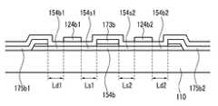
도 6은 본 발명의 다른 실시예에 따른 구동 트랜지스터를 도시한 개략도이며,6 is a schematic diagram illustrating a driving transistor according to another embodiment of the present invention;
도 7은 도 6의 구동 트랜지스터를 VII-VII 선을 따라 잘라 도시한 단면도이다.FIG. 7 is a cross-sectional view of the driving transistor of FIG. 6 taken along the line VII-VII. FIG.
<도면 부호의 설명>≪ Description of reference numerals &
110: 절연 기판121, 129: 게이트선110:
124a: 스위칭 제어 전극124a: switching control electrode
124b, 124b1, 124b2: 구동 제어 전극140: 게이트 절연막124b, 124b1, and 124b2: drive control electrode 140: gate insulating film
154a: 스위칭 반도체154b: 구동 반도체154a: switching
154s1, 154s2, 154d1, 154d2: 오프셋 영역154s1, 154s2, 154d1, 154d2: offset area
163a, 163b, 165a, 165b: 저항성 접촉 부재163a, 163b, 165a, 165b: resistive contact member
171, 179: 데이터선172: 구동 전압선171 and 179: data line 172: driving voltage line
173a: 스위칭 입력 전극175a: 스위칭 출력 전극173a: switching
173b: 구동 입력 전극173b: drive input electrode
175b, 175b1, 175b2: 구동 출력 전극175b, 175b1, 175b2: drive output electrode
81, 82: 접촉 보조 부재85: 연결 부재81, 82: contact assistant member 85: connecting member
180: 보호막180: shield
181, 182, 182b, 183b, 185b: 접촉 구멍181, 182, 182b, 183b, 185b: contact hole
191: 화소 전극230: 색필터191: pixel electrode 230: color filter
232b, 233b, 235b: 관통 구멍270: 공통 전극232b, 233b, and 235b: through hole 270: common electrode
361: 격벽365: 개구부361: partition 365: opening
370: 발광층370: light emitting layer
Cst: 유지 축전기ILD: 구동 전류Cst: holding capacitor ILD : driving current
LD: 유기 발광 다이오드PX: 화소LD: organic light emitting diode PX: pixel
Qs: 스위칭 트랜지스터Qd: 구동 트랜지스터Qs: switching transistor Qd: driving transistor
Vss: 공통 전압Vss: Common Voltage
본 발명은 박막 트랜지스터 및 이를 포함하는 유기 발광 표시 장치에 관한 것으로서, 특히 유기 발광 표시 장치용 오프셋 구조 박막 트랜지스터에 관한 것이다.The present invention relates to a thin film transistor and an organic light emitting display device including the same, and more particularly, to an offset structure thin film transistor for an organic light emitting display device.
액정 표시 장치 및 유기 발광 표시 장치 등 능동형 표시 장치는 행렬의 형태로 배열되어 있는 복수의 화소를 포함한다. 각 화소는 전기장 생성 전극과 적어도 하나의 트랜지스터를 포함하며, 트랜지스터는 반도체와 세 개의 단자, 즉 제어 단자, 입력 단자, 출력 단자를 가지는 박막 트랜지스터일 수 있다. 박막 트랜지스터는 게이트 신호에 응답하여 데이터 전압을 전달하거나 데이터 전압에 비례하는 양의 전류를 생성한다.An active display device such as a liquid crystal display and an organic light emitting display includes a plurality of pixels arranged in a matrix form. Each pixel includes an electric field generating electrode and at least one transistor, and the transistor may be a thin film transistor having a semiconductor and three terminals, that is, a control terminal, an input terminal, and an output terminal. The thin film transistor delivers a data voltage in response to the gate signal or generates a positive current proportional to the data voltage.
이러한 표시 장치의 표시판은 다수의 도전층과 절연층으로 이루어진 적층 구조를 가진다. 제어 전극, 입력 및 출력 전극, 전기장 생성 전극 등은 서로 다른 도전층으로 형성되며, 절연층으로 분리되어 있다.The display panel of such a display device has a laminated structure composed of a plurality of conductive layers and an insulating layer. The control electrode, the input and output electrodes, the field generating electrode and the like are formed of different conductive layers, and are separated by an insulating layer.
이러한 적층 구조에서, 박막 트랜지스터는 역스태거드 하부 게이트 방식(inverse staggered bottom gate) 방식 또는 스태거드 상부 게이트(staggered top gate) 방식으로 만들어질 수 있다.In such a stacked structure, the thin film transistor may be made of an inverse staggered bottom gate method or a staggered top gate method.
스태거드 상부 게이트 방식의 박막 트랜지스터의 경우, 맨 아래에 반도체가 위치하고, 그 위에 입력 및 출력 전극이 있으며, 맨 위에 게이트 전극이 위치한다. 이때 게이트 전극은 게이트 절연막을 사이에 두고 반도체와 중첩할 뿐 아니라 입력 및 출력 전극과 중첩하는 것이 일반적이다.In the case of a staggered upper gate type thin film transistor, a semiconductor is positioned at the bottom, an input and an output electrode thereon, and a gate electrode is positioned at the top. In this case, the gate electrode generally overlaps the semiconductor with the gate insulating layer interposed therebetween, and overlaps the input and output electrodes.
그런데 입력 및 출력 전극의 경계 부근에서 게이트 절연막의 경사 분포가 트랜지스터에 따라 달라질 수 있으며 이에 따라 제어 전극의 단면 모양도 달라질 수 있다. 제어 전극의 단면 모양이 달라지면, 게이트 전극이 생성하는 전기장의 모양도 달라지며 이에 따라 트랜지스터가 구동하는 전류의 크기도 달라질 수 있다.However, the inclination distribution of the gate insulating layer near the boundary between the input and output electrodes may vary according to the transistor, and accordingly, the cross-sectional shape of the control electrode may also vary. If the cross-sectional shape of the control electrode is changed, the shape of the electric field generated by the gate electrode is also changed, and thus the magnitude of the current driven by the transistor may be changed.
이를 방지하기 위하여 제어 전극이 입력 및 출력 전극과 겹치지 않도록 설계할 수 있으며, 이 경우 제어 전극과 입력 및 출력 전극 사이의 반도체 부분에 오프셋 영역이 만들어진다.In order to prevent this, the control electrode may be designed so as not to overlap the input and output electrodes. In this case, an offset region is formed in a semiconductor portion between the control electrode and the input and output electrodes.
한편, 표시판은 통상 노광 및 식각을 통하여 만들어지는데, 모 기판이 큰 경우 노광 공정에서는 기판을 여러 영역으로 쪼개어 차례로 노광하는 분할 노광을 적용한다.On the other hand, the display panel is usually made through exposure and etching, and in the case of a large substrate, an exposure process applies a divided exposure in which the substrate is divided into several regions and sequentially exposed.
그런데 노광 과정에서 마스크의 전이(shift), 회전(rotation), 비틀림(distortion) 등의 왜곡이 발생하기 때문에 영역 별로 층간 정렬의 정도가 다를 수 있다. 또한, 분할 노광을 적용하지 않는다고 하더라도 장비의 정밀도 여부에 따라 어느 정도의 층간 정렬 오차가 생기는 것이 대부분이다.However, since distortion such as shift, rotation, and distortion of the mask occurs during the exposure process, the degree of interlayer alignment may be different for each region. In addition, even if the split exposure is not applied, most of the interlayer alignment errors are generated depending on the accuracy of the equipment.
특히 박막 트랜지스터의 제어 전극과 입력 전극 사이의 거리와 제어 전극과 출력 전극 사이의 거리가 달라지는 경우, 제어 전극 양쪽의 오프 셋 영역의 길이가 차이가 나므로 오프 셋 영역의 저항값과 이에 따른 전류값이 편차가 생길 수 있다.In particular, when the distance between the control electrode and the input electrode and the distance between the control electrode and the output electrode of the thin film transistor is different, the length of the offset region of both control electrodes is different, so the resistance value of the offset region and the corresponding current value are different. Deviation may occur.
따라서 본 발명이 이루고자 하는 기술적 과제는 정렬 오차 및 편차와 관계 없는 박막 트랜지스터를 제공하는 것이다.Therefore, the technical problem to be achieved by the present invention is to provide a thin film transistor that is independent of alignment error and deviation.
본 발명의 한 실시예에 따른 박막 트랜지스터는, 한 방향으로 배열되어 있으며 서로 분리되어 있는 제1 내지 제5 전극 영역 및 상기 제1 내지 제5 전극 영역 사이에 위치한 제1 내지 제4 오프셋 영역을 포함하는 반도체, 상기 제3 전극 영역과 전기적으로 연결되어 있는 입력 전극, 상기 제1 및 제5 전극 영역과 전기적으로 연결되어 있는 출력 전극, 상기 반도체 위에 형성되어 있는 절연막, 그리고 상기 절연막 위에 형성되어 있으며 상기 제2 및 제4 전극 영역 위에 위치하는 제어 전극을 포함한다.A thin film transistor according to an exemplary embodiment of the present invention includes first to fifth electrode regions arranged in one direction and separated from each other, and first to fourth offset regions disposed between the first to fifth electrode regions. A semiconductor, an input electrode electrically connected to the third electrode region, an output electrode electrically connected to the first and fifth electrode regions, an insulating film formed on the semiconductor, and an insulating film formed on the insulating film. And a control electrode positioned over the second and fourth electrode regions.
상기 반도체는 다결정 규소 또는 미세 결정질 규소일 수 있다.The semiconductor may be polycrystalline silicon or microcrystalline silicon.
상기 반도체와 상기 제어 전극, 상기 입력 전극 및 상기 출력 전극 사이에 위치한 복수의 저항성 접촉 부재를 더 수 있다.A plurality of ohmic contacts may be further disposed between the semiconductor and the control electrode, the input electrode, and the output electrode.
상기 박막 트랜지스터는 상기 저항성 접촉 부재는 불순물을 포함하는 다결정 규소 또는 미세 결정질 규소를 포함할 수 있다.In the thin film transistor, the ohmic contact member may include polycrystalline silicon or microcrystalline silicon including impurities.
상기 절연막은 질화규소 또는 산화규소를 포함할 수 있다.The insulating film may include silicon nitride or silicon oxide.
본 발명의 한 실시예에 따른 유기 발광 표시 장치는, 공통 전압과 연결되어 있는 유기 발광 소자, 상기 유기 발광 소자 및 구동 전압과 연결되어 있는 구동 트랜지스터, 상기 구동 트랜지스터와 연결되어 있는 스위칭 트랜지스터, 상기 스위칭 트랜지스터와 연결되어 있는 게이트선, 그리고 상기 스위칭 트랜지스터와 연결되어 있으며 상기 게이트선과 절연되어 있는 데이터선을 포함한다. 상기 구동 트랜지스 터는, 한 방향으로 배열되어 있으며 서로 분리되어 있는 제1 내지 제5 전극 영역 및 상기 제1 내지 제5 전극 영역 사이에 위치한 제1 내지 제4 오프셋 영역을 포함하는 결정질 반도체, 상기 제3 전극 영역 및 구동 전압과 연결되어 있는 제1 입력 전극, 상기 제1 및 제5 전극 영역 및 상기 유기 발광 소자와 연결되어 있는 제1 출력 전극, 상기 결정질 반도체 위에 형성되어 있는 게이트 절연막, 그리고 상기 게이트 절연막 위에 형성되어 있고 상기 제2 및 제4 전극 영역 위에 위치하며, 상기 스위칭 트랜지스터와 연결되어 있는 제1 제어 전극을 포함한다.An organic light emitting diode display according to an exemplary embodiment of the present invention includes an organic light emitting diode connected to a common voltage, a driving transistor connected to the organic light emitting diode and a driving voltage, a switching transistor connected to the driving transistor, and the switching. A gate line connected to the transistor, and a data line connected to the switching transistor and insulated from the gate line. The driving transistor is a crystalline semiconductor including first to fifth electrode regions arranged in one direction and separated from each other, and first to fourth offset regions positioned between the first to fifth electrode regions. A first input electrode connected to a three electrode region and a driving voltage, a first output electrode connected to the first and fifth electrode regions, and the organic light emitting element, a gate insulating layer formed on the crystalline semiconductor, and the gate And a first control electrode formed on the insulating layer and positioned on the second and fourth electrode regions and connected to the switching transistor.
상기 스위칭 트랜지스터는 상기 게이트 절연막 위에 형성되어 있는 비정질 반도체를 포함할 수 있다.The switching transistor may include an amorphous semiconductor formed on the gate insulating layer.
상기 스위칭 박막 트랜지스터는, 상기 게이트 절연막 아래에 형성되어 있으며 상기 게이트선과 연결되어 있는 제2 제어 전극, 상기 비정질 반도체 위에 형성되어 있으며 상기 데이터선과 연결되어 있는 제2 입력 전극, 그리고 상기 비정질 반도체 위에 형성되어 있고, 상기 제2 입력 전극과 분리되어 있으며, 상기 제1 제어 전극과 연결되어 있는 스위칭 출력 전극을 더 포함할 수 있다.The switching thin film transistor is formed under the gate insulating film and is connected to the gate line, the second input electrode is formed on the amorphous semiconductor and is connected to the data line, and is formed on the amorphous semiconductor. And a switching output electrode separated from the second input electrode and connected to the first control electrode.
상기 구동 트랜지스터는 상기 결정질 반도체와 상기 제1 제어 전극, 상기 제1 입력 전극 및 상기 제1 출력 전극 사이에 위치한 복수의 저항성 접촉 부재를 더 포함할 수 있다.The driving transistor may further include a plurality of ohmic contacts between the crystalline semiconductor and the first control electrode, the first input electrode, and the first output electrode.
상기 저항성 접촉 부재는 불순물을 포함하는 다결정 규소 또는 미세 결정질 규소를 포함할 수 있다.The ohmic contact member may include polycrystalline silicon or microcrystalline silicon including impurities.
상기 절연막은 질화규소 또는 산화규소를 포함할 수 있다.The insulating film may include silicon nitride or silicon oxide.
상기 유기 발광 표시 장치는 상기 유기 발광 소자와 중첩하는 색필터를 더 포함하며, 상기 유기 발광 소자는 백색 광을 방출할 수 있다.The organic light emitting diode display may further include a color filter overlapping the organic light emitting diode, and the organic light emitting diode may emit white light.
그러면, 첨부한 도면을 참고로 하여 본 발명의 실시예에 대하여 본 발명이 속하는 기술 분야에서 통상의 지식을 가진 자가 용이하게 실시할 수 있도록 상세히 설명한다.Hereinafter, embodiments of the present invention will be described in detail with reference to the accompanying drawings so that those skilled in the art can easily carry out the present invention.
도면에서 여러 층 및 영역을 명확하게 표현하기 위하여 두께를 확대하여 나타내었다. 명세서 전체를 통하여 유사한 부분에 대해서는 동일한 도면 부호를 붙였다. 층, 막, 영역, 판 등의 부분이 다른 부분 "위에" 있다고 할 때, 이는 다른 부분 "바로 위에" 있는 경우뿐 아니라 그 중간에 또 다른 부분이 있는 경우도 포함한다. 반대로 어떤 부분이 다른 부분 "바로 위에" 있다고 할 때에는 중간에 다른 부분이 없는 것을 뜻한다.In the drawings, the thickness is enlarged to clearly represent the layers and regions. Like parts are designated with like reference numerals throughout the specification. It will be understood that when an element such as a layer, film, region, plate, or the like is referred to as being "on" another portion, it includes not only the element directly over another element, Conversely, when a part is "directly over" another part, it means that there is no other part in the middle.
먼저 본 발명의 한 실시예에 따른 표시 장치의 대표적인 예로서 유기 발광 표시 장치에 대하여 도 1을 참고로 상세하게 설명한다.First, an organic light emitting display device is described in detail with reference to FIG. 1 as a representative example of a display device according to an exemplary embodiment of the present invention.
도 1은 본 발명의 한 실시예에 따른 유기 발광 표시 장치의 등가 회로도이다.1 is an equivalent circuit diagram of an OLED display according to an embodiment of the present invention.
도 1을 참고하면, 본 실시예에 따른 유기 발광 표시 장치는 복수의 신호선(121, 171, 172)과 이들에 연결되어 있으며 대략 행렬(matrix)의 형태로 배열된 복수의 화소(pixel)(PX)를 포함한다.Referring to FIG. 1, the organic light emitting diode display according to the present exemplary embodiment includes a plurality of
신호선은 게이트 신호(또는 주사 신호)를 전달하는 복수의 게이트선(gate line)(121), 데이터 신호를 전달하는 복수의 데이터선(data line)(171) 및 구동 전 압을 전달하는 복수의 구동 전압선(driving voltage line)(172)을 포함한다. 게이트선(121)은 대략 행 방향으로 뻗어 있으며 서로가 거의 평행하고 데이터선(171)과 구동 전압선(172)은 대략 열 방향으로 뻗어 있으며 서로가 거의 평행하다.The signal line includes a plurality of
각 화소(PX)는 스위칭 트랜지스터(switching transistor)(Qs), 구동 박막 트랜지스터(driving transistor)(Qd), 유지 축전기(storage capacitor)(Cst) 및 유기 발광 다이오드(organic light emitting diode, OLED)(LD)를 포함한다.Each pixel PX includes a switching transistor Qs, a driving transistor Qd, a storage capacitor Cst, and an organic light emitting diode OLED. ).
스위칭 트랜지스터(Qs)는 제어 단자(control terminal), 입력 단자(input terminal) 및 출력 단자(output terminal)를 가지는데, 제어 단자는 게이트선(121)에 연결되어 있고, 입력 단자는 데이터선(171)에 연결되어 있으며, 출력 단자는 구동 트랜지스터(Qd)에 연결되어 있다. 스위칭 트랜지스터(Qs)는 게이트선(121)으로부터 받은 주사 신호에 응답하여 데이터선(171)으로부터 받은 데이터 신호를 구동 트랜지스터(Qd)에 전달한다.The switching transistor Qs has a control terminal, an input terminal and an output terminal. The control terminal is connected to the
구동 트랜지스터(Qd) 또한 제어 단자, 입력 단자 및 출력 단자를 가지는데, 제어 단자는 스위칭 트랜지스터(Qs)에 연결되어 있고, 입력 단자는 구동 전압선(172)에 연결되어 있으며, 출력 단자는 유기 발광 다이오드(LD)에 연결되어 있다. 구동 트랜지스터(Qd)는 제어 단자와 출력 단자 사이에 걸리는 전압에 따라 그 크기가 달라지는 출력 전류(ILD)를 흘린다.The driving transistor Qd also has a control terminal, an input terminal and an output terminal, the control terminal being connected to the switching transistor Qs, the input terminal being connected to the driving
축전기(Cst)는 구동 트랜지스터(Qd)의 제어 단자와 입력 단자 사이에 연결되어 있다. 이 축전기(Cst)는 구동 트랜지스터(Qd)의 제어 단자에 인가되는 데이터 신호를 충전하고 스위칭 트랜지스터(Qs)가 턴 오프(turn-off)된 뒤에도 이를 유지한다.The capacitor Cst is connected between the control terminal and the input terminal of the driving transistor Qd. The capacitor Cst charges the data signal applied to the control terminal of the driving transistor Qd and maintains it even after the switching transistor Qs is turned off.
유기 발광 다이오드(LD)는 구동 트랜지스터(Qd)의 출력 단자에 연결되어 있는 애노드(anode)와 공통 전압(Vss)에 연결되어 있는 캐소드(cathode)를 가진다. 유기 발광 다이오드(LD)는 구동 트랜지스터(Qd)의 출력 전류(ILD)에 따라 세기를 달리하여 발광함으로써 영상을 표시한다.The organic light emitting diode LD has an anode connected to the output terminal of the driving transistor Qd and a cathode connected to the common voltage Vss. The organic light emitting diode LD displays an image by emitting light having a different intensity depending on the output current ILD of the driving transistor Qd.
스위칭 트랜지스터(Qs) 및 구동 트랜지스터(Qd)는 n-채널 전계 효과 트랜지스터(field effect transistor, FET)이다. 그러나 스위칭 트랜지스터(Qs)와 구동 트랜지스터(Qd) 중 적어도 하나는 p-채널 전계 효과 트랜지스터일 수 있다. 또한, 트랜지스터(Qs, Qd), 축전기(Cst) 및 유기 발광 다이오드(LD)의 연결 관계가 바뀔 수 있다.The switching transistor Qs and the driving transistor Qd are n-channel field effect transistors (FETs). However, at least one of the switching transistor Qs and the driving transistor Qd may be a p-channel field-effect transistor. In addition, the connection relationship between the transistors Qs and Qd, the capacitor Cst, and the organic light emitting diode LD may be changed.
그러면 도 1에 도시한 유기 발광 표시 장치의 상세 구조에 대하여 도 2 및 도 3을 도 1과 함께 참고하여 상세하게 설명한다. Next, detailed structures of the organic light emitting diode display illustrated in FIG. 1 will be described in detail with reference to FIGS. 2 and 3.
도 2는 본 발명의 한 실시예에 따른 유기 발광 표시 장치의 배치도이고, 도 3은 도 2의 유기 발광 표시 장치를 III-III 선을 따라 잘라 도시한 단면도이다.2 is a layout view of an organic light emitting diode display according to an exemplary embodiment, and FIG. 3 is a cross-sectional view of the organic light emitting diode display of FIG. 2 taken along a line III-III.
투명한 유리 또는 플라스틱 따위로 만들어진 절연 기판(110) 위에 복수의 구동 트랜지스터용 섬형 반도체(semiconductor island)(앞으로 "구동 반도체"라 함)(154b)가 형성되어 있다. 구동 반도체(154b)는 미세 결정질 규소(microcrystalline silicon) 및 다결정 규소(polycrystalline silicon) 따위의 결정질 반도체로 만들어질 수 있다.A plurality of island islands for driving transistors (hereinafter referred to as "drive semiconductors") 154b are formed on an insulating
구동 반도체(154b) 위에는 각각 세 개의 구동 트랜지스터용 저항성 접촉 부재[ohmic contact (island)](앞으로 "구동 저항성 접촉 부재"라 함)(163b, 165b)가 형성되어 있다. 세 개의 구동 저항성 접촉 부재(163b, 165b)는 섬 모양이며 세로 방향으로 일렬로 배치되어 있다. 구동 저항성 접촉 부재(163a, 163b)는 인 따위의 n형 불순물이 고농도로 도핑되어 있는 n+ 미세 결정질 규소 및 다결정 규소 따위의 결정질 반도체로 만들어질 수 있다.Three ohmic contacts (island) (hereinafter referred to as " drive resistive contact members ") for driving transistors are formed on the
기판(110) 및 구동 저항성 접촉 부재(163b, 165b) 위에는 복수의 게이트선(gate line)(121)과 복수의 구동 트랜지스터용 입력 전극(input electrode)(앞으로 "구동 입력 전극"이라 함)(173b) 및 복수의 구동 트랜지스터용 출력 전극(output electrode)(앞으로 "구동 출력 전극"이라 함)(175b)이 형성되어 있다.A plurality of
게이트선(121)은 기판(110) 위에 위치하고, 게이트 신호를 전달하며 주로 가로 방향으로 뻗어 있다. 각 게이트선(121)은 위로 뻗어 있는 스위칭 트랜지스터용 제어 전극(control electrode)(앞으로 "스위칭 제어 전극"이라 함)(124a)과 다른 층 또는 외부 구동 회로와의 접속을 위하여 면적이 넓은 끝 부분(129)을 포함한다. 게이트 신호를 생성하는 게이트 구동 회로(도시하지 않음)가 기판(110) 위에 집적되어 있는 경우 게이트선(121)이 연장되어 게이트 구동 회로와 직접 연결될 수 있다.The
구동 입력 전극(173b) 및 구동 출력 전극(175b)은 게이트선(121)과 분리되어 있으며, 각각 구동 저항성 접촉 부재(163b, 165b) 및 기판(110) 위에 위치한다. 구동 출력 전극(175b)은 두 갈래로 갈라져 구동 입력 전극(173b)의 양쪽에 위치한다.The driving
구동 저항성 접촉 부재(163b, 165b)는 그 아래의 구동 반도체(154b)와 그 위의 구동 입력 전극(173b) 및 구동 출력 전극(175b) 사이에만 존재하며 접촉 저항을 낮추어 준다. 구동 반도체(154b)에는 구동 입력 전극(173b)과 구동 출력 전극(175b) 사이를 비롯하여 이들로 가리지 않고 노출된 부분이 있다.The driving
게이트선(110), 구동 입력 전극(173b) 및 구동 출력 전극(175b)은 몰리브덴(Mo), 크롬(Cr), 탄탈륨(Ta) 및 티타늄(Ti) 등 내화성 금속 또는 이들의 합금으로 만들어질 수 있으며, 내화성 금속막(도시하지 않음)과 저저항 도전막(도시하지 않음)을 포함하는 다중막 구조를 가질 수 있다. 다중막 구조의 예로는 크롬 또는 몰리브덴 (합금) 하부막과 알루미늄 (합금) 상부막의 이중막, 몰리브덴 (합금) 하부막과 알루미늄 (합금) 중간막과 몰리브덴 (합금) 상부막의 삼중막을 들 수 있다. 그러나 게이트선(121), 구동 입력 전극(173b) 및 구동 출력 전극(175b)은 이외에도 여러 가지 다양한 금속 또는 도전체로 만들어질 수 있다.The
게이트선(121), 구동 입력 전극(173b) 및 구동 출력 전극(175b)은 기판(110) 면에 대하여 경사져 있으며 그 경사각은 약 30도 내지 약 80도인 것이 바람직하다.The
게이트선(121), 구동 입력 전극(173b) 및 구동 출력 전극(175b) 및 노출된 구동 반도체(154b) 부분 위에는 산화규소(SiO2) 또는 질화규소(SiNx) 따위로 만들어진 게이트 절연막(140)이 형성되어 있다.A
게이트 절연막(140) 위에는 수소화 비정질 규소(hydrogenated amorphous silicon)로 만들어진 복수의 스위칭 트랜지스터용 섬형 반도체(앞으로 "스위칭 반도체"라 함)(154a)가 형성되어 있다. 스위칭 반도체(154a)는 스위칭 제어 전극(124a) 위에 위치한다.On the
스위칭 반도체(154a) 위에는 복수 쌍의 스위칭 트랜지스터용 저항성 접촉 부재(앞으로 "스위칭 저항성 접촉 부재"라 함)(163a, 165a)가 형성되어 있다. 스위칭 저항성 접촉 부재(163a, 163b)는 섬 모양이며, 인 따위의 n형 불순물이 고농도로 도핑되어 있는 n+ 수소화 비정질 규소 따위의 물질로 만들어질 수 있다.A plurality of pairs of resistive contact members (hereinafter referred to as " switching resistive contact members ") 163a and 165a are formed on the switching
스위칭 저항성 접촉 부재(163a, 163b) 및 게이트 절연막(140) 위에는 복수의 데이터선(171), 복수의 구동 전압선(172) 및 복수의 전극 부재(176)가 형성되어 있다.A plurality of
데이터선(171)은 데이터 신호를 전달하며 주로 세로 방향으로 뻗어 게이트선(121)과 교차한다. 각 데이터선(171)은 스위칭 제어 전극(124a)을 향하여 뻗은 복수의 스위칭 트랜지스터용 입력 전극(앞으로 "스위칭 입력 전극"이라 함)(173a)과 다른 층 또는 외부 구동 회로와의 접속을 위하여 면적이 넓은 끝 부분(179)을 포함한다. 데이터 신호를 생성하는 데이터 구동 회로(도시하지 않음)가 기판(110) 위에 집적되어 있는 경우, 데이터선(171)이 연장되어 데이터 구동 회로와 직접 연결될 수 있다.The
구동 전압선(172)은 구동 전압을 전달하며 주로 세로 방향으로 뻗어 게이트선(121)과 교차한다.The driving
전극 부재(176)는 데이터선(171) 및 구동 전압선(172)과 분리되어 있다. 전극 부재(176)는 각각 스위칭 트랜지스터용 출력 전극(앞으로 "스위칭 출력 전극"이라 한다)(175a)과 구동 트랜지스터용 제어 전극(앞으로 "구동 제어 전극"이라 한다)(124b)을 포함한다.The
스위칭 출력 전극(175a)은 스위칭 저항성 접촉 부재(165a) 위에 위치하며 스위칭 입력 전극(173a)과 마주한다.The switching
구동 제어 전극(124b)은 두 갈래로 갈라져 구동 반도체(154b) 위에 위치한다. 구동 제어 전극(124b)의 갈라진 분지들은 각각 구동 입력 전극(173b)과 구동 출력 전극(175b)의 사이에 위치한다.The driving
데이터선(171), 구동 전압선(172) 및 전극 부재(176)는 게이트선(121)과 동일한 재료로 만들어질 수 있다.The
데이터선(171), 구동 전압선(172) 및 전극 부재(176)의 측면은 기판(110) 면에 대하여 경사져 있으며 그 경사각은 약 30도 내지 약 80도일 수 있다.Side surfaces of the
스위칭 저항성 접촉 부재(163a, 163b)는 그 아래의 스위칭 반도체(154a)와 그 위의 데이터선(171) 및 전극 부재(176) 사이에만 존재하며 접촉 저항을 낮추어 준다. 스위칭 반도체(154a)에는 스위칭 입력 전극(173a)과 스위칭 출력 전극(175a) 사이를 비롯하여 이들로 가리지 않고 노출된 부분이 있다.The switching
데이터선(171), 구동 전압선(172), 전극 부재(176) 및 노출된 스위칭 반도체(154a) 부분 위에는 복수의 색 필터(color filter)(230)가 형성되어 있다. 그러나 유기 발광 표시 장치가 백색 화소를 포함하는 경우, 백색 화소에는 색 필터가 없거나 투명한 백색 필터(도시하지 않음)가 있을 수 있다.A plurality of
색 필터(230)는 데이터선(171) 너비의 일부 및 구동 전압선(172)의 전체 너비를 덮으며, 복수의 관통 구멍(232b, 233b, 235b)을 가진다. 관통 구멍(232b)은 구동 전압선(172)을 드러내고, 관통 구멍(233b)은 구동 입력 전극(173b)을 드러내며, 관통 구멍(235b)은 구동 출력 전극(175b)을 드러낸다.The
색 필터(230B)의 가장자리는 데이터선(171) 및 게이트선(121) 위에서 중첩될 수 있으며, 중첩된 부분은 화소 사이에서 누설되는 빛을 차단할 수 있다.An edge of the color filter 230B may overlap the
색 필터(230)의 아래에는 층간 절연막(도시하지 않음)이 형성될 수 있다. 층간 절연막은 색 필터(230)의 안료가 스위칭 반도체(154a)로 유입되는 것을 방지할 수 있다.An interlayer insulating layer (not shown) may be formed under the
색 필터(230B), 데이터선(171), 구동 전압선(172) 및 전극 부재(176) 위에는 보호막(passivation layer)(180)이 형성되어 있다. 보호막(180)은 무기 절연물 또는 유기 절연물 따위로 만들어지며 표면이 평탄할 수 있다. 무기 절연물의 예로는 질화규소와 산화규소를 들 수 있다. 유기 절연물은 감광성(photosensitivity)을 가질 수 있으며 그 유전 상수(dielectric constant)는 약 4.0 이하인 것이 바람직하다.A
보호막(180)에는 데이터선(171)의 끝 부분(179)을 드러내는 복수의 접촉 구멍(182) 및 관통 구멍(232b)을 통하여 구동 전압선(172)을 드러내는 복수의 접촉 구멍(contact hole)(182b)이 형성되어 있다. 보호막(180) 및 게이트 절연막(140)에는 게이트선(121)의 끝 부분(129)을 드러내는 복수의 접촉 구멍(181), 관통 구 멍(233b)을 통하여 구동 입력 전극(173b)을 드러내는 복수의 접촉 구멍(183b), 그리고 관통 구멍(235b)을 통하여 구동 출력 전극(175b)을 드러내는 복수의 접촉 구멍(185b)이 형성되어 있다.The
보호막(180) 위에는 복수의 화소 전극(pixel electrode)(191), 복수의 연결 부재(85) 및 복수의 접촉 보조 부재(contact assistant)(81, 82)가 형성되어 있다.A plurality of
화소 전극(191)은 접촉 구멍(185b)을 통하여 구동 출력 전극(175b)과 연결되어 있다.The
연결 부재(85)는 접촉 구멍(182b, 183b)을 통하여 구동 전압선(172) 및 구동 입력 전극(173b)과 연결되어 있으며, 구동 제어 전극(124b)과 일부 중첩하여 유지 축전기(storage capacitor)(Cst)를 이룰 수 있다.The
접촉 보조 부재(81, 82)는 각각 접촉 구멍(181, 182)을 통하여 게이트선(121)의 끝 부분(129) 및 데이터선(171)의 끝 부분(179)과 연결된다. 접촉 보조 부재(81, 82)는 게이트선(121) 및 데이터선(171)의 끝 부분(129, 179)과 외부 장치와의 접착성을 보완하고 이들을 보호한다.The
화소 전극(191), 연결 부재(85) 및 접촉 보조 부재(81, 82)는 ITO 또는 IZO 따위의 투명 도전체로 만들어질 수 있다.The
화소 전극(191) 및 연결 부재(85) 위에는 절연성 둑(insulating bank)(361)이 형성되어 있다. 둑(361)은 화소 전극(191) 가장자리 주변을 둘러싸서 개구부(opening)(365)를 정의한다.An insulating
둑(361) 및 화소 전극(191) 위에는 백색 광을 방출하는 발광층(370)이 형성 되어 있다.A
발광층(370)은, 예를 들면 적색, 녹색 및 청색 빛을 고유하게 내는 유기 물질이 상하로 차례로 적층되거나 동일한 평면 상에 나란하게 배치된 구조를 가질 수 있다.For example, the
발광층(370)은 고분자 물질 또는 저분자 물질로 만들어질 수 있다. 고분자 물질의 예로는 폴리플루오렌(polyfluorene) 유도체, (폴리)파라페닐렌비닐렌((poly)paraphenylenevinylene) 유도체, 폴리페닐렌(polyphenylene) 유도체, 폴리비닐카바졸(polyvinylcarbazole), 폴리티오펜(polythiophene) 유도체 등을 들 수 있다. 저분자 물질로는 9,10-디페닐안트라센(9,10-diphenylanthracene)과 같은 안트라센(anthracene), 테트라페닐부타디엔(tetraphenylbutadiene)과 같은 부타디엔(butadiene), 테트라센(tetracene), 디스티릴아릴렌(distyrylarylene) 유도체, 벤자졸(benzazole) 유도체 및 카바졸(carbazole) 유도체 등의 예가 있다. 이와는 달리, 앞에서 기재한 고분자 물질 또는 저분자 물질을 주 재료(host material)로 하고, 여기에 크산텐(xanthene), 페릴렌(perylene), 쿠마린(cumarine), 로더민(rhodamine), 루브렌(rubrene), 디시아노메틸렌피란(dicyanomethylenepyran) 화합물, 티오피란(thiopyran) 화합물, (티아)피릴리움((thia)pyrilium) 화합물, 페리플란텐(periflanthene) 유도체, 인데노페릴렌(indenoperylene) 유도체, 카보스티릴(carbostyryl) 화합물, 나일 레드(Nile red), 퀴나크리돈(quinacridone) 따위의 도펀트(dopant)를 도핑하여 발광 효율을 높일 수도 있다.The
발광층(370)의 양면에는 발광층(370)의 발광 효율을 향상하기 위한 부대 층(auxiliary layer)(도시하지 않음)이 형성될 수 있다.An auxiliary layer (not shown) may be formed on both surfaces of the
부대층에는 전자와 정공의 균형을 맞추기 위한 전자 수송층(electron transport layer)(도시하지 않음) 및 정공 수송층(hole transport layer)(도시하지 않음)과 전자와 정공의 주입을 강화하기 위한 전자 주입층(electron injecting layer)(도시하지 않음) 및 정공 주입층(hole injecting layer)(도시하지 않음) 등이 있다.The auxiliary layer includes an electron transport layer (not shown) and a hole transport layer (not shown) for balancing electrons and holes, and an electron injection layer for enhancing the injection of electrons and holes ( electron injecting layers (not shown) and hole injecting layers (not shown).
발광층(370) 위에는 공통 전극(common electrode)(270)이 형성되어 있다. 공통 전극(270)은 공통 전압(Vss)을 인가 받으며, 일 함수가 낮고 반사율이 높은 금속으로 만들어질 수 있다. 이러한 물질의 예로는 알루미늄 또는 알루미늄 합금, 금(Au), 백금(Pt), 니켈(Ni), 구리(Cu), 텅스텐(W) 또는 이들의 합금을 들 수 있다.The
이러한 유기 발광 표시 장치에서, 화소 전극(191), 발광층(370) 및 공통 전극(270)은 유기 발광 다이오드(LD)를 이루며, 화소 전극(191)이 애노드(anode), 공통 전극(270)이 캐소드(cathode)가 되거나 반대로 화소 전극(191)이 캐소드, 공통 전극(270)이 애노드가 된다.In the OLED display, the
또한, 게이트선(121)에 연결되어 있는 스위칭 제어 전극(124a), 데이터선(171)에 연결되어 있는 스위칭 입력 전극(173a) 및 스위칭 출력 전극(175a)은 스위칭 반도체(154a)와 함께 스위칭 박막 트랜지스터(thin film transistor, TFT)(Qs)를 이루며, 스위칭 박막 트랜지스터(Qs)의 채널(channel)은 스위칭 입력 전극(173a)과 스위칭 출력 전극(175a) 사이의 스위칭 반도체(154a)에 형성된다.In addition, the switching
스위칭 출력 전극(175a)에 연결되어 있는 구동 제어 전극(124b), 구동 전압선(172)에 연결되어 있는 구동 입력 전극(173b) 및 화소 전극(191)에 연결되어 있는 구동 출력 전극(175b)은 구동 반도체(154b)와 함께 구동 박막 트랜지스터(Qd)를 이루며, 구동 박막 트랜지스터(Qd)의 채널은 구동 입력 전극(173b)과 구동 출력 전극(175b) 사이의 구동 반도체(154b)에 형성된다.The driving
앞에서 설명했듯이, 스위칭 반도체(154a)는 비정질 반도체로 만들어지고, 구동 반도체(154b)는 결정질 반도체로 만들어진다.As described above, the switching
이와 같이 스위칭 박막 트랜지스터(Qs)와 구동 박막 트랜지스터(Qd)의 채널은 결정 상태가 다른 반도체에 형성되며, 이에 따라 각 박막 트랜지스터에서 요구되는 특성을 동시에 만족할 수 있다.As described above, the channels of the switching thin film transistor Qs and the driving thin film transistor Qd are formed in semiconductors having different crystal states, thereby simultaneously satisfying the characteristics required for each thin film transistor.
구동 트랜지스터(Qd)에 사용되는 결정질 반도체는 전하 이동도(carrier mobility)가 높으므로, 유기 발광 다이오드(LD)에 흐르는 전류량을 크게 하여 휘도를 높일 수 있다. 결정질 반도체를 적용한 구동 트랜지스터(Qd)는 문턱 전압 이동 현상(threshold voltage shift)이 거의 없으므로 이미지 고착(image sticking) 및 수명 단축이 줄어든다.Since the crystalline semiconductor used in the driving transistor Qd has high carrier mobility, the luminance of the crystalline semiconductor may be increased by increasing the amount of current flowing through the organic light emitting diode LD. The driving transistor Qd adopting the crystalline semiconductor has little threshold voltage shift, thereby reducing image sticking and shortening the lifespan.
스위칭 박막 트랜지스터(Qs)에 사용되는 비정질 반도체는 오프 전류가 작으므로 데이터 전압의 하강과 크로스토크(crosstalk)가 줄어든다.The amorphous semiconductor used in the switching thin film transistor Qs has a small off current, so that the data voltage falls and crosstalk is reduced.
본 발명의 다른 실시예에 따르면, 각 화소(PX)는 스위칭 트랜지스터(Qs) 하나와 구동 트랜지스터(Qd) 하나 외에도 유기 발광 다이오드(LD) 및 구동 트랜지스터(Qd)의 열화를 방지 또는 보상하는 다른 트랜지스터를 더 포함할 수 있다.According to another exemplary embodiment of the present invention, each pixel PX may include another switching transistor Qs and one driving transistor Qd to prevent or compensate for degradation of the organic light emitting diode LD and the driving transistor Qd. It may further include.
그러면, 도 2 및 도 3에 도시한 유기 발광 표시 장치에서 구동 트랜지스터의 구조에 대하여 도 4 내지 도 7을 참고하여 더욱 상세하게 설명한다.Next, the structure of the driving transistor in the OLED display illustrated in FIGS. 2 and 3 will be described in more detail with reference to FIGS. 4 to 7.
도 4는 본 발명의 한 실시예에 따른 구동 트랜지스터를 도시한 개략도이고, 도 5는 도 4의 구동 트랜지스터를 V-V 선을 따라 잘라 도시한 단면도이며, 도 6은 본 발명의 다른 실시예에 따른 구동 트랜지스터를 도시한 개략도이고, 도 7은 도 6의 구동 트랜지스터를 VII-VII 선을 따라 잘라 도시한 단면도이다.4 is a schematic diagram illustrating a driving transistor according to an embodiment of the present invention, FIG. 5 is a cross-sectional view of the driving transistor of FIG. 4 taken along a line VV, and FIG. 6 is a driving diagram according to another embodiment of the present invention. 7 is a schematic diagram illustrating a transistor, and FIG. 7 is a cross-sectional view of the driving transistor of FIG. 6 taken along the line VII-VII.
도 4 및 도 5는 입력 전극(173b) 및 출력 전극(175b)이 제어 전극(124b)을 중심으로 정확하게 대칭으로 배열되어 있는 상태를 보여준다. 즉, 제어 전극(124b)의 제1 가지(124b1)에서부터 입력 전극(173b)까지의 거리(Ls1), 제어 전극(124b)의 제1 가지(124b1)에서부터 출력 전극(175b)의 제1 가지(175b1)까지의 거리(Ld1), 제어 전극(124b)의 제2 가지(124b2)에서부터 입력 전극(173b)까지의 거리(Ls2), 제어 전극(124b)의 제2 가지(124b2)에서부터 출력 전극(175b)의 제2 가지(175b2)까지의 거리(Ld2)가 모두 동일하다. 다시 말하면, 반도체(154b)의 네 오프셋 영역(offset region)(154s1, 154d1, 154s2, 154d2)이 길이가 모두 동일하다.4 and 5 show a state in which the
그러므로 제어 전극(124b)과 입력 전극(173b) 사이의 오프셋 영역(154s1, 154s2)의 저항과 제어 전극(124b)과 출력 전극(173b) 사이의 오프셋 영역(154d1, 154d2)의 저항은 동일하다.Therefore, the resistances of the offset regions 154s1 and 154s2 between the
반도체(154b)에서 오프셋 영역(154s1, 154d1, 154s2, 154d2)을 제외한 다른 영역, 즉 전극 영역(electrode region)들은 입력 전극(173b), 출력 전극(175b)의 두 가지(175b1, 175b2) 및 제어 전극(124b)의 두 가지(124b1, 124b2)와 연결되어 있거나 중첩한다.In the
도 6 및 도 7은 입력 전극(173b) 및 출력 전극(175b)이 제어 전극(124b)을 기준으로 위로 치우치게 배열되어 있는 상태를 보여준다. 즉, 오프셋 영역(154s1)의 길이(Ls1)와 오프셋 영역(154d1)의 길이(Ld1)가 다르고, 오프셋 영역(154s2)의 길이(Ls2)와 오프셋 영역(154d2)의 길이(Ld2)도 다르다.6 and 7 illustrate a state in which the
그러나 도 4 및 도 5와 비교하여 볼 때, 오프셋 영역(154s1)의 길이(Ls1)가 줄어든 만큼 오프셋 영역(154d1)의 길이(Ld1)가 늘고, 오프셋 영역(154s2)의 길이(Ls2)가 늘어난 만큼 오프셋 영역(154d2)의 길이(Ld2)가 줄어든다. 또한 오프셋 영역(154s1)의 길이(Ls1) 축소분과 오프셋 영역(154s2)의 길이(Ls2) 증가분이 동일하고, 오프셋 영역(154d1)의 길이(Ld1) 증가분과 오프셋 영역(154d2)의 길이(Ld2) 축소분이 동일하다.However, as compared with FIGS. 4 and 5, the length Ld1 of the offset region 154d1 increases and the length Ls2 of the offset region 154s2 increases as the length Ls1 of the offset region 154s1 decreases. The length Ld2 of the offset area 154d2 is reduced by this amount. Further, the length Ls1 reduction of the offset area 154s1 and the length Ls2 increase of the offset area 154s2 are equal, and the length Ld1 increase of the offset area 154d1 and the length Ld2 of the offset area 154d2 are the same. The reduction is the same.
그러므로 제어 전극(124b)과 입력 전극(173b) 사이의 오프셋 영역(154s1, 154s2)의 길이의 합(=Ls1+Ls2)과 제어 전극(124b)과 출력 전극(173b) 사이의 오프셋 영역(154d1, 154d2)의 길이의 합((=Ld1+Ld2))은 동일하다. 이에 따라 입력 쪽 저항과 출력 쪽 저항 또한 동일하며, 이 구동 트랜지스터가 구동하는 전류량 또한 일정하다.Therefore, the sum of the lengths of the offset regions 154s1 and 154s2 between the
앞에서 설명한 유기 발광 표시 장치는 기판(110)의 아래쪽으로 빛을 내보내어 영상을 표시하는 배면 발광(bottom emission) 방식이다. 그러나 불투명한 화소 전극(191)과 투명한 공통 전극(270)을 포함하며 기판(110)의 아래 방향으로 영상을 표시하는 전면 발광(top emission) 방식의 유기 발광 표시 장치에도 본 발명이 적 용될 수 있다. 이 경우 색 필터(230)는 발광층(370)의 위에 위치한다.The organic light emitting diode display described above is a bottom emission method that emits light toward the bottom of the
본 발명은 또한 다른 구조의 유기 발광 표시 장치와 액정 표시 장치 등 다른 표시 장치에도 적용할 수 있다.The present invention can also be applied to other display devices such as organic light emitting display devices and liquid crystal display devices having other structures.
이와 같이 정렬 오차 및 편차에 관계 없이 오프셋 저항의 길이가 일정한 박막 트랜지스터를 얻을 수 있다.In this manner, a thin film transistor having a constant length of an offset resistor can be obtained regardless of alignment error and deviation.
이상에서 본 발명의 바람직한 실시예들에 대하여 상세하게 설명하였지만 본 발명의 권리 범위는 이에 한정되는 것은 아니고 다음의 청구 범위에서 정의하고 있는 본 발명의 기본 개념을 이용한 당업자의 여러 변형 및 개량 형태 또한 본 발명의 권리 범위에 속하는 것이다.While the present invention has been particularly shown and described with reference to exemplary embodiments thereof, it is to be understood that the invention is not limited to the disclosed exemplary embodiments, And falls within the scope of the invention.
Claims (19)
Translated fromKoreanPriority Applications (4)
| Application Number | Priority Date | Filing Date | Title |
|---|---|---|---|
| KR1020070027501AKR101293570B1 (en) | 2007-03-21 | 2007-03-21 | Thin film transistor and organic light emitting device including thin film transistor |
| US11/858,863US7671366B2 (en) | 2007-03-21 | 2007-09-20 | Thin film transistor and organic light emitting device including thin film transistor |
| CNA2008100822335ACN101271925A (en) | 2007-03-21 | 2008-02-26 | Thin film transistor and organic light emitting device including same |
| EP08004000AEP1973164A3 (en) | 2007-03-21 | 2008-03-04 | Thin film transistor and organic light emitting device including thin film transistor |
Applications Claiming Priority (1)
| Application Number | Priority Date | Filing Date | Title |
|---|---|---|---|
| KR1020070027501AKR101293570B1 (en) | 2007-03-21 | 2007-03-21 | Thin film transistor and organic light emitting device including thin film transistor |
Publications (2)
| Publication Number | Publication Date |
|---|---|
| KR20080085985A KR20080085985A (en) | 2008-09-25 |
| KR101293570B1true KR101293570B1 (en) | 2013-08-06 |
Family
ID=39537455
Family Applications (1)
| Application Number | Title | Priority Date | Filing Date |
|---|---|---|---|
| KR1020070027501AActiveKR101293570B1 (en) | 2007-03-21 | 2007-03-21 | Thin film transistor and organic light emitting device including thin film transistor |
Country Status (4)
| Country | Link |
|---|---|
| US (1) | US7671366B2 (en) |
| EP (1) | EP1973164A3 (en) |
| KR (1) | KR101293570B1 (en) |
| CN (1) | CN101271925A (en) |
Families Citing this family (9)
| Publication number | Priority date | Publication date | Assignee | Title |
|---|---|---|---|---|
| JP2009231643A (en)* | 2008-03-24 | 2009-10-08 | Casio Comput Co Ltd | Optical sensing element, photosensor, and display device |
| KR101540341B1 (en)* | 2008-10-17 | 2015-07-30 | 삼성전자주식회사 | PANEL STRUCTURE, DISPLAY DEVICE COMPRISING PANEL STRUCTURE AND METHOD FOR MANUFACTURING |
| TWI464869B (en) | 2011-07-14 | 2014-12-11 | Au Optronics Corp | Semiconductor element and electroluminescent element and manufacturing method thereof |
| CN102339835A (en)* | 2011-07-14 | 2012-02-01 | 友达光电股份有限公司 | Semiconductor component, electroluminescent component and manufacturing method thereof |
| JP6623078B2 (en)* | 2016-02-23 | 2019-12-18 | 株式会社ブイ・テクノロジー | Laser annealing method and laser annealing apparatus |
| JP6857488B2 (en)* | 2016-11-29 | 2021-04-14 | 株式会社日立製作所 | Manufacturing method of semiconductor devices |
| WO2018138603A1 (en) | 2017-01-26 | 2018-08-02 | Semiconductor Energy Laboratory Co., Ltd. | Semiconductor device and electronic device including the semiconductor device |
| KR102432663B1 (en)* | 2017-11-30 | 2022-08-12 | 엘지디스플레이 주식회사 | Electroluminescent Display Device |
| KR102588659B1 (en)* | 2018-06-26 | 2023-10-12 | 삼성디스플레이 주식회사 | Display device |
Citations (3)
| Publication number | Priority date | Publication date | Assignee | Title |
|---|---|---|---|---|
| KR20030061586A (en)* | 2002-01-15 | 2003-07-22 | 비오이 하이디스 테크놀로지 주식회사 | Thin film transistor and fabricating method thereof |
| US20030214248A1 (en) | 2002-04-26 | 2003-11-20 | Yushi Jinno | Dim-out method for organic EL panel |
| JP2006235612A (en) | 2005-01-31 | 2006-09-07 | Semiconductor Energy Lab Co Ltd | Display device and electronic device |
Family Cites Families (26)
| Publication number | Priority date | Publication date | Assignee | Title |
|---|---|---|---|---|
| JPS5990958A (en)* | 1982-11-16 | 1984-05-25 | Nec Corp | Semiconductor device |
| US6323071B1 (en)* | 1992-12-04 | 2001-11-27 | Semiconductor Energy Laboratory Co., Ltd. | Method for forming a semiconductor device |
| JPH06275644A (en) | 1993-03-22 | 1994-09-30 | Sharp Corp | Thin film transistor and manufacturing method thereof |
| US5847413A (en)* | 1994-08-31 | 1998-12-08 | Semiconductor Energy Laboratory Co., Ltd. | Differential amplifier circuit and analog buffer |
| JP4293434B2 (en) | 1994-08-31 | 2009-07-08 | 株式会社半導体エネルギー研究所 | Liquid crystal display |
| TW329500B (en) | 1995-11-14 | 1998-04-11 | Handotai Energy Kenkyusho Kk | Electro-optical device |
| JP3522442B2 (en) | 1996-03-11 | 2004-04-26 | 株式会社半導体エネルギー研究所 | Thin film semiconductor device |
| JPH09307111A (en) | 1996-05-10 | 1997-11-28 | Sony Corp | Semiconductor device |
| JPH1079514A (en) | 1996-09-05 | 1998-03-24 | Toshiba Corp | Active matrix substrate manufacturing method |
| CN100341042C (en)* | 1997-02-17 | 2007-10-03 | 精工爱普生株式会社 | Display device |
| JP3092553B2 (en) | 1997-09-24 | 2000-09-25 | 日本電気株式会社 | Insulated gate field effect transistor |
| KR100269521B1 (en)* | 1997-11-01 | 2000-10-16 | 구본준 | Thin film transistor and its manufacturing method |
| KR100274546B1 (en) | 1998-08-21 | 2000-12-15 | 윤종용 | Thin film transistor and manufacturing method thereof |
| JP3524029B2 (en) | 2000-01-04 | 2004-04-26 | インターナショナル・ビジネス・マシーンズ・コーポレーション | Method of forming top gate type TFT structure |
| US6791144B1 (en)* | 2000-06-27 | 2004-09-14 | International Business Machines Corporation | Thin film transistor and multilayer film structure and manufacturing method of same |
| JP4011292B2 (en)* | 2001-01-15 | 2007-11-21 | 株式会社日立製作所 | LIGHT EMITTING ELEMENT AND DISPLAY DEVICE |
| KR100477103B1 (en) | 2001-12-19 | 2005-03-18 | 삼성에스디아이 주식회사 | TFT with Multiple Gates and Fabrication Method thereof using MILC |
| US6955932B2 (en)* | 2003-10-29 | 2005-10-18 | International Business Machines Corporation | Single and double-gate pseudo-FET devices for semiconductor materials evaluation |
| KR100640213B1 (en)* | 2003-12-29 | 2006-10-31 | 엘지.필립스 엘시디 주식회사 | Polysilicon Liquid Crystal Display Device Manufacturing Method |
| US7371625B2 (en) | 2004-02-13 | 2008-05-13 | Semiconductor Energy Laboratory Co., Ltd. | Semiconductor device and manufacturing method thereof, liquid crystal television system, and EL television system |
| KR100662790B1 (en)* | 2004-12-28 | 2007-01-02 | 엘지.필립스 엘시디 주식회사 | LCD and its manufacturing method |
| JP4887647B2 (en)* | 2005-03-31 | 2012-02-29 | 凸版印刷株式会社 | Method for manufacturing thin film transistor device |
| KR101100423B1 (en) | 2005-04-12 | 2011-12-30 | 삼성전자주식회사 | Method of forming silicon thin film transistor, gate insulating layer of silicon thin film transistor and manufacturing method of silicon thin film transistor using same |
| KR101107697B1 (en) | 2005-04-19 | 2012-01-25 | 엘지디스플레이 주식회사 | Thin film transistor and liquid crystal display device having same |
| US7537976B2 (en)* | 2005-05-20 | 2009-05-26 | Semiconductor Energy Laboratory Co., Ltd. | Manufacturing method of thin film transistor |
| JP2007128049A (en)* | 2005-10-03 | 2007-05-24 | Sanyo Electric Co Ltd | Display panel |
- 2007
- 2007-03-21KRKR1020070027501Apatent/KR101293570B1/enactiveActive
- 2007-09-20USUS11/858,863patent/US7671366B2/enactiveActive
- 2008
- 2008-02-26CNCNA2008100822335Apatent/CN101271925A/enactivePending
- 2008-03-04EPEP08004000Apatent/EP1973164A3/ennot_activeWithdrawn
Patent Citations (3)
| Publication number | Priority date | Publication date | Assignee | Title |
|---|---|---|---|---|
| KR20030061586A (en)* | 2002-01-15 | 2003-07-22 | 비오이 하이디스 테크놀로지 주식회사 | Thin film transistor and fabricating method thereof |
| US20030214248A1 (en) | 2002-04-26 | 2003-11-20 | Yushi Jinno | Dim-out method for organic EL panel |
| JP2006235612A (en) | 2005-01-31 | 2006-09-07 | Semiconductor Energy Lab Co Ltd | Display device and electronic device |
Also Published As
| Publication number | Publication date |
|---|---|
| CN101271925A (en) | 2008-09-24 |
| US7671366B2 (en) | 2010-03-02 |
| EP1973164A2 (en) | 2008-09-24 |
| EP1973164A3 (en) | 2012-03-21 |
| US20080230768A1 (en) | 2008-09-25 |
| KR20080085985A (en) | 2008-09-25 |
Similar Documents
| Publication | Publication Date | Title |
|---|---|---|
| KR101293570B1 (en) | Thin film transistor and organic light emitting device including thin film transistor | |
| KR101219036B1 (en) | Organic light emitting diode display | |
| KR101293562B1 (en) | Organic light emitting diode display and method for manufacturing the same | |
| KR101240651B1 (en) | Display device and method for manufacturing the same | |
| US7863602B2 (en) | Organic light emitting diode display and method for manufacturing the same | |
| KR101251998B1 (en) | Organic light emitting diode display and method for manufacturing the same | |
| KR101209038B1 (en) | Organic light emitting diode display | |
| US7883921B2 (en) | Thin film transistor array panel and manufacturing method thereof | |
| KR101600816B1 (en) | Organic Light Emitting Diode Display and Manufacturing Method thereof | |
| KR20070081829A (en) | OLED display and manufacturing method thereof | |
| KR20070037848A (en) | Organic light emitting display | |
| JP2007329138A (en) | Dual panel type organic electroluminescent device and manufacturing method thereof | |
| US7646044B2 (en) | Thin film transistor and thin film transistor array panel | |
| KR20070082685A (en) | Display device and manufacturing method thereof | |
| CN113903751A (en) | Thin film transistor array substrate and display device | |
| KR20070054806A (en) | Organic light emitting display | |
| KR101240648B1 (en) | Organic light emitting diode display and method for manufacturing the same | |
| KR101100885B1 (en) | Thin film transistor array panel for organic light emitting display | |
| EP1970957A2 (en) | Thin film transistor, an organic light emitting device including the same, and a manufacturing method thereof | |
| KR20070059559A (en) | Display device and manufacturing method thereof | |
| KR101240649B1 (en) | Organic light emitting diode display and method for manufacturing the same | |
| KR20080092716A (en) | Organic light emitting device and organic light emitting display device including the same | |
| KR20070052509A (en) | Organic light emitting display | |
| KR20080053646A (en) | Manufacturing Method of Organic Light Emitting Display | |
| KR101143008B1 (en) | Organic light emitting diode display |
Legal Events
| Date | Code | Title | Description |
|---|---|---|---|
| PA0109 | Patent application | Patent event code:PA01091R01D Comment text:Patent Application Patent event date:20070321 | |
| PG1501 | Laying open of application | ||
| A201 | Request for examination | ||
| PA0201 | Request for examination | Patent event code:PA02012R01D Patent event date:20120321 Comment text:Request for Examination of Application Patent event code:PA02011R01I Patent event date:20070321 Comment text:Patent Application | |
| N231 | Notification of change of applicant | ||
| PN2301 | Change of applicant | Patent event date:20120913 Comment text:Notification of Change of Applicant Patent event code:PN23011R01D | |
| E701 | Decision to grant or registration of patent right | ||
| PE0701 | Decision of registration | Patent event code:PE07011S01D Comment text:Decision to Grant Registration Patent event date:20130514 | |
| GRNT | Written decision to grant | ||
| PR0701 | Registration of establishment | Comment text:Registration of Establishment Patent event date:20130731 Patent event code:PR07011E01D | |
| PR1002 | Payment of registration fee | Payment date:20130731 End annual number:3 Start annual number:1 | |
| PG1601 | Publication of registration | ||
| FPAY | Annual fee payment | Payment date:20160629 Year of fee payment:4 | |
| PR1001 | Payment of annual fee | Payment date:20160629 Start annual number:4 End annual number:4 | |
| FPAY | Annual fee payment | Payment date:20170704 Year of fee payment:5 | |
| PR1001 | Payment of annual fee | Payment date:20170704 Start annual number:5 End annual number:5 | |
| FPAY | Annual fee payment | Payment date:20180702 Year of fee payment:6 | |
| PR1001 | Payment of annual fee | Payment date:20180702 Start annual number:6 End annual number:6 | |
| FPAY | Annual fee payment | Payment date:20190701 Year of fee payment:7 | |
| PR1001 | Payment of annual fee | Payment date:20190701 Start annual number:7 End annual number:7 | |
| PR1001 | Payment of annual fee | Payment date:20200701 Start annual number:8 End annual number:8 | |
| PR1001 | Payment of annual fee | Payment date:20210701 Start annual number:9 End annual number:9 | |
| PR1001 | Payment of annual fee | Payment date:20220620 Start annual number:10 End annual number:10 | |
| PR1001 | Payment of annual fee | Payment date:20240625 Start annual number:12 End annual number:12 |