KR101285907B1 - Electronic interface apparatus and method and system for manufacturing same - Google Patents
Electronic interface apparatus and method and system for manufacturing sameDownload PDFInfo
- Publication number
- KR101285907B1 KR101285907B1KR1020097024350AKR20097024350AKR101285907B1KR 101285907 B1KR101285907 B1KR 101285907B1KR 1020097024350 AKR1020097024350 AKR 1020097024350AKR 20097024350 AKR20097024350 AKR 20097024350AKR 101285907 B1KR101285907 B1KR 101285907B1
- Authority
- KR
- South Korea
- Prior art keywords
- substrate
- layer
- chip module
- metal members
- antenna
- Prior art date
- Legal status (The legal status is an assumption and is not a legal conclusion. Google has not performed a legal analysis and makes no representation as to the accuracy of the status listed.)
- Expired - Fee Related
Links
Images


Classifications
- G—PHYSICS
- G06—COMPUTING OR CALCULATING; COUNTING
- G06K—GRAPHICAL DATA READING; PRESENTATION OF DATA; RECORD CARRIERS; HANDLING RECORD CARRIERS
- G06K19/00—Record carriers for use with machines and with at least a part designed to carry digital markings
- G06K19/06—Record carriers for use with machines and with at least a part designed to carry digital markings characterised by the kind of the digital marking, e.g. shape, nature, code
- G06K19/067—Record carriers with conductive marks, printed circuits or semiconductor circuit elements, e.g. credit or identity cards also with resonating or responding marks without active components
- G06K19/07—Record carriers with conductive marks, printed circuits or semiconductor circuit elements, e.g. credit or identity cards also with resonating or responding marks without active components with integrated circuit chips
- G06K19/077—Constructional details, e.g. mounting of circuits in the carrier
- G06K19/07745—Mounting details of integrated circuit chips
- G—PHYSICS
- G06—COMPUTING OR CALCULATING; COUNTING
- G06K—GRAPHICAL DATA READING; PRESENTATION OF DATA; RECORD CARRIERS; HANDLING RECORD CARRIERS
- G06K19/00—Record carriers for use with machines and with at least a part designed to carry digital markings
- G06K19/06—Record carriers for use with machines and with at least a part designed to carry digital markings characterised by the kind of the digital marking, e.g. shape, nature, code
- G06K19/067—Record carriers with conductive marks, printed circuits or semiconductor circuit elements, e.g. credit or identity cards also with resonating or responding marks without active components
- G06K19/07—Record carriers with conductive marks, printed circuits or semiconductor circuit elements, e.g. credit or identity cards also with resonating or responding marks without active components with integrated circuit chips
- G06K19/077—Constructional details, e.g. mounting of circuits in the carrier
- G06K19/07749—Constructional details, e.g. mounting of circuits in the carrier the record carrier being capable of non-contact communication, e.g. constructional details of the antenna of a non-contact smart card
- G06K19/0775—Constructional details, e.g. mounting of circuits in the carrier the record carrier being capable of non-contact communication, e.g. constructional details of the antenna of a non-contact smart card arrangements for connecting the integrated circuit to the antenna
- G06K19/07754—Constructional details, e.g. mounting of circuits in the carrier the record carrier being capable of non-contact communication, e.g. constructional details of the antenna of a non-contact smart card arrangements for connecting the integrated circuit to the antenna the connection being galvanic
- G—PHYSICS
- G06—COMPUTING OR CALCULATING; COUNTING
- G06K—GRAPHICAL DATA READING; PRESENTATION OF DATA; RECORD CARRIERS; HANDLING RECORD CARRIERS
- G06K19/00—Record carriers for use with machines and with at least a part designed to carry digital markings
- G06K19/06—Record carriers for use with machines and with at least a part designed to carry digital markings characterised by the kind of the digital marking, e.g. shape, nature, code
- G06K19/067—Record carriers with conductive marks, printed circuits or semiconductor circuit elements, e.g. credit or identity cards also with resonating or responding marks without active components
- G06K19/07—Record carriers with conductive marks, printed circuits or semiconductor circuit elements, e.g. credit or identity cards also with resonating or responding marks without active components with integrated circuit chips
- G06K19/077—Constructional details, e.g. mounting of circuits in the carrier
- G06K19/07749—Constructional details, e.g. mounting of circuits in the carrier the record carrier being capable of non-contact communication, e.g. constructional details of the antenna of a non-contact smart card
- G06K19/07773—Antenna details
- H—ELECTRICITY
- H01—ELECTRIC ELEMENTS
- H01L—SEMICONDUCTOR DEVICES NOT COVERED BY CLASS H10
- H01L2924/00—Indexing scheme for arrangements or methods for connecting or disconnecting semiconductor or solid-state bodies as covered by H01L24/00
- H01L2924/0001—Technical content checked by a classifier
- H01L2924/0002—Not covered by any one of groups H01L24/00, H01L24/00 and H01L2224/00
- Y—GENERAL TAGGING OF NEW TECHNOLOGICAL DEVELOPMENTS; GENERAL TAGGING OF CROSS-SECTIONAL TECHNOLOGIES SPANNING OVER SEVERAL SECTIONS OF THE IPC; TECHNICAL SUBJECTS COVERED BY FORMER USPC CROSS-REFERENCE ART COLLECTIONS [XRACs] AND DIGESTS
- Y10—TECHNICAL SUBJECTS COVERED BY FORMER USPC
- Y10T—TECHNICAL SUBJECTS COVERED BY FORMER US CLASSIFICATION
- Y10T29/00—Metal working
- Y10T29/49—Method of mechanical manufacture
- Y10T29/49002—Electrical device making
- Y10T29/49016—Antenna or wave energy "plumbing" making
- Y10T29/49018—Antenna or wave energy "plumbing" making with other electrical component
- Y—GENERAL TAGGING OF NEW TECHNOLOGICAL DEVELOPMENTS; GENERAL TAGGING OF CROSS-SECTIONAL TECHNOLOGIES SPANNING OVER SEVERAL SECTIONS OF THE IPC; TECHNICAL SUBJECTS COVERED BY FORMER USPC CROSS-REFERENCE ART COLLECTIONS [XRACs] AND DIGESTS
- Y10—TECHNICAL SUBJECTS COVERED BY FORMER USPC
- Y10T—TECHNICAL SUBJECTS COVERED BY FORMER US CLASSIFICATION
- Y10T29/00—Metal working
- Y10T29/49—Method of mechanical manufacture
- Y10T29/49002—Electrical device making
- Y10T29/49117—Conductor or circuit manufacturing
- Y10T29/49124—On flat or curved insulated base, e.g., printed circuit, etc.
- Y10T29/4913—Assembling to base an electrical component, e.g., capacitor, etc.
- Y—GENERAL TAGGING OF NEW TECHNOLOGICAL DEVELOPMENTS; GENERAL TAGGING OF CROSS-SECTIONAL TECHNOLOGIES SPANNING OVER SEVERAL SECTIONS OF THE IPC; TECHNICAL SUBJECTS COVERED BY FORMER USPC CROSS-REFERENCE ART COLLECTIONS [XRACs] AND DIGESTS
- Y10—TECHNICAL SUBJECTS COVERED BY FORMER USPC
- Y10T—TECHNICAL SUBJECTS COVERED BY FORMER US CLASSIFICATION
- Y10T29/00—Metal working
- Y10T29/49—Method of mechanical manufacture
- Y10T29/49002—Electrical device making
- Y10T29/49117—Conductor or circuit manufacturing
- Y10T29/49169—Assembling electrical component directly to terminal or elongated conductor
- Y—GENERAL TAGGING OF NEW TECHNOLOGICAL DEVELOPMENTS; GENERAL TAGGING OF CROSS-SECTIONAL TECHNOLOGIES SPANNING OVER SEVERAL SECTIONS OF THE IPC; TECHNICAL SUBJECTS COVERED BY FORMER USPC CROSS-REFERENCE ART COLLECTIONS [XRACs] AND DIGESTS
- Y10—TECHNICAL SUBJECTS COVERED BY FORMER USPC
- Y10T—TECHNICAL SUBJECTS COVERED BY FORMER US CLASSIFICATION
- Y10T29/00—Metal working
- Y10T29/53—Means to assemble or disassemble
- Y10T29/5313—Means to assemble electrical device
- Y10T29/5317—Laminated device
- Y—GENERAL TAGGING OF NEW TECHNOLOGICAL DEVELOPMENTS; GENERAL TAGGING OF CROSS-SECTIONAL TECHNOLOGIES SPANNING OVER SEVERAL SECTIONS OF THE IPC; TECHNICAL SUBJECTS COVERED BY FORMER USPC CROSS-REFERENCE ART COLLECTIONS [XRACs] AND DIGESTS
- Y10—TECHNICAL SUBJECTS COVERED BY FORMER USPC
- Y10T—TECHNICAL SUBJECTS COVERED BY FORMER US CLASSIFICATION
- Y10T29/00—Metal working
- Y10T29/53—Means to assemble or disassemble
- Y10T29/5313—Means to assemble electrical device
- Y10T29/53174—Means to fasten electrical component to wiring board, base, or substrate
- Y10T29/53178—Chip component
Landscapes
- Engineering & Computer Science (AREA)
- Microelectronics & Electronic Packaging (AREA)
- Computer Hardware Design (AREA)
- Physics & Mathematics (AREA)
- General Physics & Mathematics (AREA)
- Theoretical Computer Science (AREA)
- Computer Networks & Wireless Communication (AREA)
- Credit Cards Or The Like (AREA)
- Details Of Aerials (AREA)
Abstract
Translated fromKoreanDescription
Translated fromKorean본 발명은, 일반적으로 스마트카드(smart cards)로 알려진 전자식 인터페이스 카드(interface cards)에 관한 것으로, 더욱 상세하게는 접촉(contact) 및/또는 무접촉(contact-less) 기능을 가진 전자식 인터페이스 카드에 관한 것이다.FIELD OF THE INVENTION The present invention relates to electronic interface cards, generally known as smart cards, and more particularly to electronic interface cards having contact and / or contact-less functionality. It is about.
미합중국 특허(제7,278,580; 2,271,039; 7,269,021; 7,243,840; 7,240,847; 및 7,204,427)는 종래기술의 현황을 나타낸 것으로 여겨진다.United States patents (7,278,580; 2,271,039; 7,269,021; 7,243,840; 7,240,847; and 7,204,427) are believed to represent the state of the art.
본 발명은, 개선된 전자식 인터페이스 카드 및 그 제조 방법을 제공하고자 한다.The present invention seeks to provide an improved electronic interface card and a method of manufacturing the same.
따라서 본 발명의 바람직한 실시예에 따라, 기판 층에 1쌍의 개구부(aperture)들을 한정하는 단계; 안테나를, 상기 안테나의 대향(opposite) 단부들이 상기 개구부들에서 끝나도록, 상기 기판 층과 결합(associate)하는 단계; 상기 개구부들의 각각 내에 금속부재들을 배치하는 단계; 상기 안테나의 상기 단부들을 상기 금속부재들에 연결(connect)하는 단계; 상기 기판 층을 상부 층 및 하부 층과 함께 적층(laminate)하는 단계; 상기 상부 층 및 상기 기판 층에 홈부(recess)를 형성하는 단계; 상기 금속부재들에 연결선들의 단부들을 부착하는 단계; 상기 연결선들의 대향 단부들을 칩 모듈(chip module)에 부착하는 단계; 및 상기 홈부에 상기 칩 모듈을 밀봉하는 단계를 포함하는 전자식 인터페이스 카드의 제조 방법이 제공된다.Thus, in accordance with a preferred embodiment of the present invention, defining a pair of apertures in the substrate layer; Associating an antenna with the substrate layer such that opposite ends of the antenna terminate in the openings; Disposing metal members in each of the openings; Connecting the ends of the antenna to the metal members; Laminating the substrate layer with an upper layer and a lower layer; Forming recesses in the top layer and the substrate layer; Attaching end portions of connecting lines to the metal members; Attaching opposite ends of the connecting lines to a chip module; And sealing the chip module in the groove portion.
바람직하게는, 또한 상기 방법은, 상기 적층하는 단계 전에, 상기 기판 층의 하면 상에 제1 추가 기판 층과 제2 추가 기판 층을 제공하는 단계를 더 포함한다. 부가적으로 또는 양자택일적으로, 상기 상부 층은, 제1 상부 기판 층과 제2 상부 기판 층을 포함한다. 부가적으로, 또한 상기 방법은, 상기 홈부에 인접한 상기 제2 상부 층의 단차면(recessed surface)을 노출시키는 단계를 더 포함하고, 상기 밀봉하는 단계는, 상기 칩 모듈의 하면 상에 접착제(adhesive)를 배치하는 단계; 및 상기 하면이 상기 단차면에 맞닿도록 상기 홈부에 상기 칩 모듈을 삽입하는 단계를 포함한다.Advantageously, the method further comprises providing a first additional substrate layer and a second additional substrate layer on the bottom surface of said substrate layer before said laminating. Additionally or alternatively, the top layer includes a first top substrate layer and a second top substrate layer. Additionally, the method further includes exposing a recessed surface of the second top layer adjacent the groove, wherein the sealing comprises an adhesive on the bottom surface of the chip module. Placing); And inserting the chip module into the groove so that the bottom surface contacts the step surface.
바람직하게는, 또한 상기 방법은, 상기 칩 모듈 아래에서 상기 연결선들을 구부리는 단계를 더 포함한다. 부가적으로 또는 양자택일적으로, 상기 방법은 자동화된다.Advantageously, the method further comprises bending said connection lines under said chip module. Additionally or alternatively, the method is automated.
바람직하게는, 상기 금속부재들에 상기 연결선들의 단부들을 부착하는 단계는 레이저 접합(laser bonding) 단계를 포함한다. 부가적으로 또는 양자택일적으로, 상기 칩 모듈에 상기 연결선들의 대향 단부를 부착하는 단계는 납땜(soldering) 단계를 포함한다.Advantageously, attaching the ends of the connecting lines to the metal members comprises a laser bonding step. Additionally or alternatively, attaching opposite ends of the leads to the chip module includes soldering.
바람직하게는, 상기 연결선들은, 전자식 인터페이스 카드에서의 상기 연결선들 각각의 대향 단부들 사이의 거리보다 실질적으로 더 큰 길이를 가진다.Preferably, the leads have a length substantially greater than the distance between opposite ends of each of the leads in the electronic interface card.
또한 본 발명의 다른 바람직한 실시예에 따라, 1개 이상의 층을 가진 기판을 형성하는 단계; 상기 1개 이상의 층에 안테나를 형성하는 단계; 상기 1개 이상의 층에 홈부를 형성하는 단계; 칩 모듈과 상기 안테나 사이에 연결선들을 연결하는 단계; 및 상기 홈부에 상기 칩 모듈을 탑재하는 단계를 포함하는 전자식 인터페이스 카드의 제조 방법이 제공된다.According to another preferred embodiment of the present invention, there is also provided a method of forming a substrate having at least one layer; Forming an antenna on the at least one layer; Forming grooves in the one or more layers; Connecting connecting lines between the chip module and the antenna; And mounting the chip module in the groove portion.
바람직하게는, 상기 연결선들은, 상기 전자식 인터페이스 카드에서의 상기 연결선들 각각의 대향 단부들 사이의 거리보다 실질적으로 더 큰 길이를 가진다. 부가적으로 또는 양자택일적으로, 상기 연결선들을 연결하는 단계는, 상기 안테나를 금속부재들에 연결하는 단계; 및 상기 연결선들을 상기 금속부재들에 연결하는 단계를 포함한다. 부가적으로 또는 양자택일적으로, 상기 탑재하는 단계는, 상기 칩 모듈 아래에서 상기 연결선들을 구부리는 단계를 포함한다.Advantageously, said connecting lines have a length substantially greater than the distance between opposite ends of each of said connecting lines in said electronic interface card. Additionally or alternatively, connecting the connecting lines may include: connecting the antenna to metal members; And connecting the connection lines to the metal members. Additionally or alternatively, the mounting includes bending the connection lines under the chip module.
바람직하게는, 상기 방법은 자동화된다.Preferably, the method is automated.
본 발명의 또 다른 바람직한 실시예에 따라, 기판; 상기 기판에 결합된 와이어 안테나(wire antenna); 상기 기판에 형성된 홈부에 탑재된 칩 모듈; 및 상기 칩 모듈과 상기 와이어 안테나 사이의 전기적 연결을 제공하는 연결선들을 포함하는 전자식 인터페이스 카드가 더 제공된다.According to another preferred embodiment of the invention, the substrate; A wire antenna coupled to the substrate; A chip module mounted on a groove formed in the substrate; And an interconnection line providing electrical connection between the chip module and the wire antenna.
바람직하게는, 상기 칩 모듈은, 패키지형(packaged) 스마트카드 칩을 포함한다. 부가적으로 또는 양자택일적으로, 상기 연결선들은, 상기 홈부 내의 상기 칩 모듈 아래에서 구부러져 있다. 부가적으로 또는 양자택일적으로, 상기 연결선들은, 상기 전자식 인터페이스 카드에서의 상기 연결선들 각각의 대향 단부들 사이의 거리보다 실질적으로 더 큰 길이를 가진다.Advantageously, said chip module comprises a packaged smart card chip. Additionally or alternatively, the leads are bent under the chip module in the groove. Additionally or alternatively, the leads have a length substantially greater than the distance between opposite ends of each of the leads in the electronic interface card.
본 발명의 또 다른 바람직한 실시예에 따라, 1개 이상의 층을 가진 기판, 상기 1개 이상의 층에 배치된 2개 이상의 금속부재들, 및 상기 기판과 결합되고, 상기 2개 이상의 금속부재들에 전기적으로 접속된 단부들을 갖는 와이어 안테나를 포함하는 전자식 인터페이스 어셈블리를 기반으로 한 전자식 인터페이스 카드를 제조하는 시스템이 더 제공되어 있고, 상기 시스템은, 상기 기판 층을 상부 층 및 하부 층과 함께 적층하도록 작동하는 적층기; 상기 상부 층 및 상기 기판 층에 홈부를 형성하도록 작동하는 홈부 형성기; 상기 금속부재들에 연결선들의 단부들을 부착하도록 작동하는 제1 연결선 부착기; 상기 연결선들의 대향 단부들을 칩 모듈에 부착하도록 작동하는 제2 연결선 부착기; 및 상기 홈부에 상기 칩 모듈을 밀봉하도록 작동하는 밀봉기를 포함한다.According to another preferred embodiment of the present invention, a substrate having one or more layers, two or more metal members disposed in the one or more layers, and coupled to the substrate and electrically connected to the two or more metal members A system is further provided for manufacturing an electronic interface card based on an electronic interface assembly that includes a wire antenna having ends connected to the system, the system operative to stack the substrate layer together with an upper layer and a lower layer. Stacker; Groove formers operative to form grooves in the top layer and the substrate layer; A first connecting line attacher operative to attach ends of the connecting lines to the metal members; A second lead wire attacher operative to attach opposite ends of said lead wires to a chip module; And a sealer operative to seal the chip module to the groove portion.
바람직하게는, 상기 제1 연결선 부착기는, 레이저 접합형 연결선 부착기이다. 부가적으로 또는 양자택일적으로, 상기 제2 연결선 부착기는, 납땜형 연결선 부착기이다.Preferably, the said 1st connection wire | attachment machine is a laser bonded connection wire | attachment machine. Additionally or alternatively, the second lead wire attacher is a soldering lead attacher.
본 발명의 또 다른 바람직한 실시예에 따라, 1개 이상의 층을 가진 기판; 상기 1개 이상의 층에 배치된 2개 이상의 금속부재들; 및 상기 기판과 결합되고, 상기 2개 이상의 금속부재들에 전기적으로 접속된 단부들을 갖는 와이어 안테나를 포함하는 전자식 인터페이스 어셈블리가 더 제공된다.According to another preferred embodiment of the present invention, there is provided a substrate comprising one or more layers; Two or more metal members disposed on the one or more layers; And a wire antenna coupled to the substrate, the wire antenna having ends electrically connected to the two or more metal members.
본 발명의 또 다른 바람직한 실시예에 따라, 1개 이상의 기판 층을 가진 기판을 제공하는 단계; 안테나를, 상기 1개 이상의 기판 층과 결합하는 단계; 및 상기 안테나의 대향 단부들을, 상기 기판과 결합된 금속부재들에 연결하는 단계를 포함하는 전자식 인터페이스 어셈블리의 제조 방법이 더 제공된다.According to another preferred embodiment of the present invention, there is provided a method comprising providing a substrate having one or more substrate layers; Coupling an antenna with the at least one substrate layer; And connecting opposite ends of the antenna to metal members coupled to the substrate.
바람직하게는, 또한 상기 방법은, 1쌍의 개구부들을, 상기 안테나의 대향 단부들이 상기 개구부들에서 끝나도록, 기판 층에서 한정하는 단계; 및 상기 연결하는 단계 전에 상기 개구부들의 각각에 상기 금속부재들을 배치하는 단계를 더 포함한다. 부가적으로 또는 양자택일적으로, 또한 상기 방법은, 상기 기판 층을 상부 층 및 하부 층과 함께 적층하는 단계를 더 포함한다. 부가적으로, 또한 상기 방법은, 상기 상부 층 및 상기 기판 층에 홈부를 형성하는 단계; 상기 금속부재들에 연결선들의 단부들을 부착하는 단계; 상기 연결선들의 대향 단부들을 칩 모듈에 부착하는 단계; 및 상기 홈부에 상기 칩 모듈을 밀봉하는 단계를 더 포함한다.Advantageously, the method further comprises: defining a pair of openings in the substrate layer such that opposite ends of said antenna terminate at said openings; And disposing the metal members in each of the openings before the connecting. Additionally or alternatively, the method also includes laminating the substrate layer together with the top layer and the bottom layer. Additionally, the method further includes forming grooves in the top layer and the substrate layer; Attaching end portions of connecting lines to the metal members; Attaching opposite ends of the connecting lines to a chip module; And sealing the chip module in the groove portion.
바람직하게는, 상기 금속부재들에 연결선들의 단부들을 부착하는 단계는, 레이저 접합 단계를 포함한다. 부가적으로 또는 양자택일적으로, 상기 연결선들의 대향 단부들을 칩 모듈에 부착하는 단계는 납땜 단계를 포함한다.Preferably, attaching the ends of the connecting lines to the metal members includes a laser bonding step. Additionally or alternatively, attaching opposing ends of the leads to the chip module includes a soldering step.
바람직하게는, 상기 방법은 자동화된다.Preferably, the method is automated.
본 발명의 또 다른 바람직한 실시예에 따라, 1개 이상의 층을 가진 기판; 상기 1개 이상의 층에 배치된 2개 이상의 단자들; 상기 기판과 결합하고, 상기 2개 이상의 단자들에 전기적으로 접속된 단부들을 갖는 와이어 안테나; 상기 기판에 형성된 홈부에 탑재된 칩 모듈; 및 상기 칩 모듈과 상기 와이어 안테나 사이의 전기적 연결을 제공하는 연결선들을 포함하는 전자식 인터페이스 어셈블리가 더 제공되고, 상기 연결선들은, 상기 전자식 인터페이스 어셈블리에서의 상기 연결선들 각각의 대향 단부들 사이의 거리보다 실질적으로 더 큰 길이를 가진다.According to another preferred embodiment of the present invention, there is provided a substrate comprising one or more layers; Two or more terminals disposed in the one or more layers; A wire antenna coupled with the substrate and having ends electrically connected to the at least two terminals; A chip module mounted on a groove formed in the substrate; And an interconnection line for providing an electrical connection between the chip module and the wire antenna, the interconnections being substantially less than the distance between opposite ends of each of the interconnection lines in the electronic interface assembly. Has a larger length.
바람직하게는, 상기 칩 모듈은, 패키지형 스마트카드 칩을 포함한다. 부가적으로 또는 양자택일적으로, 상기 연결선들은, 상기 홈부 내의 상기 칩 모듈 아래에서 구부러져 있다.Preferably, the chip module includes a packaged smart card chip. Additionally or alternatively, the leads are bent under the chip module in the groove.
본 발명은 다음의 첨부된 도면과 관련하여 후술하는 세부적인 기술로부터 보다 충분히 이해되고 인식될 것이다.The invention will be more fully understood and appreciated from the following detailed description with reference to the accompanying drawings in which:
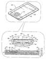
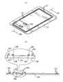
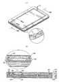
도 1은, 본 발명의 바람직한 실시예에 따라 제조되어 작동하는 접촉(contact) 기능과 무접촉(contact-less) 기능 모두를 가진 전자식 인터페이스 카드의 개략적인 사시도 및 단면도이다.1 is a schematic perspective and cross-sectional view of an electronic interface card having both a contact function and a contact-less function manufactured and operated according to a preferred embodiment of the present invention.
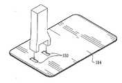
도 2는, 도 1의 전자식 인터페이스 카드의 초기 제조단계의 개략적인 사시도이다.FIG. 2 is a schematic perspective view of an initial stage of manufacture of the electronic interface card of FIG. 1.
도 3a 및 도 3b는, 각각, 도 1의 전자식 인터페이스 카드의 다른 제조단계의 개략적인 사시도 및 단면도이다.3A and 3B are schematic perspective and cross-sectional views of another manufacturing step of the electronic interface card of FIG. 1, respectively.
도 4a 및 도 4b는, 각각, 도 1의 전자식 인터페이스 카드의 또 다른 제조단 계의 개략적인 사시도 및 단면도이다.4A and 4B are schematic perspective and cross-sectional views, respectively, of another manufacturing step of the electronic interface card of FIG. 1.
도 5a 및 도 5b는, 각각, 도 1의 전자식 인터페이스 카드의 또 다른 제조단계의 개략적인 사시도 및 단면도이다.5A and 5B are schematic perspective and cross-sectional views of yet another stage of manufacture of the electronic interface card of FIG. 1, respectively.
도 6a 및 도 6b는, 각각, 도 1의 전자식 인터페이스 카드의 추가 제조 단계의 개략적인 사시도 및 단면도이다.6A and 6B are schematic perspective and cross-sectional views, respectively, of further manufacturing steps of the electronic interface card of FIG. 1.
도 7a 및 도 7b는, 각각, 도 1의 전자식 인터페이스 카드의 다른 추가 제조단계의 개략적인 사시도 및 단면도이다.7A and 7B are schematic perspective and cross-sectional views of another further manufacturing step of the electronic interface card of FIG. 1, respectively.
도 8a 및 도 8b는, 각각, 도 1의 전자식 인터페이스 카드의 또 다른 추가 제조단계의 개략적인 사시도 및 단면도이다.8A and 8B are schematic perspective and cross-sectional views of another further manufacturing step of the electronic interface card of FIG. 1, respectively.
도 9a 및 도 9b는, 각각, 도 1의 전자식 인터페이스 카드의 또 다른 추가 제조단계의 개략적인 사시도 및 단면도이다.9A and 9B are schematic perspective and cross-sectional views of yet another further manufacturing step of the electronic interface card of FIG. 1, respectively.
도 10a 및 도 10b는, 각각, 도 1의 전자식 인터페이스 카드의 마지막 제조단계의 개략적인 사시도 및 단면도이다.10A and 10B are schematic perspective and cross-sectional views, respectively, of the last stage of manufacture of the electronic interface card of FIG. 1.
이하, 본 발명을, 첨부된 도면을 참조하여 상세하게 설명하기로 한다.Hereinafter, the present invention will be described in detail with reference to the accompanying drawings.
본 발명의 바람직한 실시예에 따라 제조되어 작동하는, 접촉 및/또는 무접촉 기능을 가진 전자식 인터페이스 카드(100)를 나타낸 도 1이 참조된다. 도 1에 도시된 바와 같이, 바람직하게는, 전자식 인터페이스 카드(100)는, 일반적으로 피브이씨(PVC: PolyVinyl Chloride)로 형성되고, 각각의 두께가 일반적으로 0.05㎜가 되 는 상, 하부 보호층들(102,104)을 포함한 다층 기판을 포함한다. 한편, 보호층들(102,104)은, 테슬린(Teslin??), 피이티지(PET-G: PolyEthyleneTerephthalate-Glycol), 피이티에프(PET-F: PolyEthyleneTerephthalate-Film), 폴리카보네이트(polycarbonate) 또는 에이비에스(ABS)와 같은 다른 임의의 적합한 물질로 형성될 수 있다.Reference is made to FIG. 1, which shows an
바람직하게는, 일반적으로 피브이씨(PVC)로 형성되고, 각각의 두께가 일반적으로 0.15㎜가 되고, 각각의 보호층들(102,104)을 통하여 볼 수 있는 아트워크(artwork)를 일반적으로 가진 아트워크층들(106,108)이 보호층들(102,104) 모두의 내부에 배치된다. 한편, 아트워크층들(106,108)은, 테슬린(Teslin??), 피이티지(PET-G: PolyEthyleneTerephthalate-Glycol), 피이티에프(PET-F: PolyEthyleneTerephthalate-Film), 폴리카보네이트(polycarbonate) 또는 에이비에스(ABS)와 같은 다른 임의의 적합한 물질로 형성될 수 있다. 한편, 아트워크층들(106,108)은 제거될 수 있다.Preferably, an art generally formed of PVC, each having a thickness of generally 0.15 mm, and generally having artwork visible through the respective
바람직하게는, 일반적으로 피브이씨(PVC)로 형성되고 두께가 바람직하게는 0.15mm인 제1 인레이(inlay)층(114)에 매입되는, 와이어(wire) 직경이 바람직하게는 0.1mm인 와이어 안테나(wire antenna)(112)를 포함한 인레이(110)가 아트워크층들(106,108) 모두의 내부에 배치된다. 또한 인레이(110)는, 또한 바람직하게는 피브이씨(PVC)로 형성되고 각각의 두께가 0.1mm 및 0.15mm인 제2,3 인레이층들(116,118)을 포함한다. 한편, 제1,2,3 인레이층들(114,116,118)은, 테슬린(Teslin??), 피이티지(PET-G: PolyEthyleneTerephthalate-Glycol), 피이티에 프(PET-F: PolyEthyleneTerephthalate-Film), 폴리카보네이트(polycarbonate) 또는 에이비에스(ABS)와 같은 다른 임의의 적합한 물질로 형성될 수 있다.Preferably, the wire is preferably 0.1 mm in wire diameter, usually formed of PVC and embedded in the
칩 모듈(chip module)(120)은, 전자식 인터페이스 카드(100)에 형성된 홈부(122)에 탑재되어 있다. 바람직하게는, 칩 모듈(120)은, 패드들(pads)(126)과, 두께가 바람직하게는 0.06mm인 접촉들(contacts)(128)의 어레이(array)를 가진 패키지형 스마트카드 칩(124)을 포함하고 있다. 한편, 접촉들(128)이 제거될 수 있고, 스마트카드 칩(124)은 무접촉 기능이 제공될 수 있다.The
칩 모듈(120)과, 매입된 안테나(112) 간의 전기적 연결은, 두께가 바람직하게는 0.1mm인 연결선들(130)에 의해 제공되고, 연결선들(130)은 바람직하게는, 그 제1 단부들에서 패드들(126)에 납땜되고, 그 대향 단부들에서 와이어 안테나(112)의 각각의 단부들에 접합하는 금속부재들(132)에 레이저 접합된다. 패드들(126)과 각각의 금속부재들(132) 사이의 연결선들(130)의 길이가, 조립된 카드에서의 패드들(126)과 금속부재들(132) 사이의 거리보다 실질적으로 더 긴 것이 본 발명의 특징이다. 이러한 특징은 향상된 신뢰성을 제공한다.The electrical connection between the
접촉들(128)의 어레이의 하면 주변부에 배치된 고온용융성 접착제의 층(134)은, 층(106)의 대응하는 단차진 주변 대향면(136)에 맞닿게 함으로써 홈부(122)에 칩 모듈(120)을 계속 유지한다.The
1쌍의 개구부(150)를 형성하도록 층(114)을 천공하는, 도 1의 전자식 인터페이스 카드의 초기 제조단계의 개략적인 사시도인 도 2가 참조된다. 도 3a 및 도 3b에 도시된 바와 같이, 피시케이 테크놀로지사(PCK Technology, Inc. of islip, New York, U.S.A.)의 상업적으로 이용 가능한 초음파 헤드(ultrasonic head)를 일반적으로 채용하는 공지된 매입기술들에 의해서와 같이, 안테나(112)는 층(114)과 결합된다. 안테나(112)의 대향 단부들(152)은 도 3a 및 도 3b에 도시된 바와 같이 개구부(150)에서 끝난다.Reference is made to FIG. 2, which is a schematic perspective view of an initial stage of manufacture of the electronic interface card of FIG. 1, perforating
한편, 안테나(112)는, 적절한 인쇄법들(printing techniques)에 의해 기판(114) 상에 형성되는 인쇄식 안테나일 수 있거나, 임의의 적절한 부착방법에 의해 기판(114)에 부착된 안테나일 수 있다.On the other hand, the
도 4a 및 도 4b를 참조하면, 개구부들(150)의 대응하는 가장자리부들(156)에 있는 층(114) 상에 접착성 패드들(154)이 탑재된다. 도 5a 및 도 5b에 도시된 바와 같이, 금속부재들(132)은 개구부(150)에 배치되고, 접착성 패드들(154)에 의해 그 내에서 자리를 유지한다. 바람직하게는, 열압착접합법(thermal compression bonding) 또는 다른 임의의 적절한 기법에 의해 안테나(112)의 단부들(152)이 금속부재들(132)에 연결된다. 이러한 연결단계가 끝난 후, 접착성 패드들(154)은 더 이상 금속부재들(132)이 제자리를 유지하는데 필요하지 않고, 패드들(154)이 제거된다. 한편, 접착성 패드들(154)이 제거될 필요는 없음이 인식된다.4A and 4B,
이러한 단계에서, 도 6a 및 도 6b에 도시된 바와 같이, 층(114)의 하면 상에 층들(116,118)이 제공되고, 이층들과 함께 층들(102,104,106,108) 모두가, 도 7a 및 도 7b에 도시된 바와 같이 나타난 그 결과의 적층 구조로 적층된다.At this stage, as shown in FIGS. 6A and 6B, layers 116, 118 are provided on the bottom surface of
도 8a 및 도 8b를 참조하면, 바람직하게는 밀링(milling)에 의해, 층들(102,106,114) 및 금속부재들(132)에 홈부(122)가 형성되고, 층(106)의 단차진 주변 대향면(recessed peripheral facing surface)(136)이 노출된다. 한편, 카드의 반대면 상에 홈부가 형성될 수 있음이 인식된다. 도 9a 및 도 9b에 도시된 바와 같이, 바람직하게는 레이저 접합에 의해, 금속부재들(132)에 가는 연결선들(130)이 부착된다. 연결선들(130)은 절단되고, 바람직하게는 층(102)에 일반적으로 수직으로 연장하도록 배열된다.8A and 8B, a
도 10a 및 도 10b를 참조하면, 칩 모듈(120)의 대응하는 패드들(126)에 연결선들(130)의 부착, 및 접촉들(128)의 어레이의 하면 주변부 상에 고온용융성 접착제(134)의 배치 후에, 접촉들(128)의 어레이의 주변부가 층(106)의 단차진 주변 대향면(136)을 기밀하게 맞닿도록 홈부(122)에 칩 모듈(120)이 삽입된다. 삽입방법은, 도 1에 도시된 바와 같이 칩 모듈(120) 아래에서 연결선들(130)을 구부리는 방법이다.10A and 10B, the attachment of connecting
도 1 내지 도 10b에 관하여 상술한 방법이 바람직하게는 고도로 자동화됨이 인식된다.It is recognized that the method described above with respect to FIGS. 1-10B is preferably highly automated.
본 명세서에서 설명한 예시된 실시예가 기판 층들(102,104,106,108,114,116,118)을 포함하지만, 전자식 인터페이스 카드(100)의 다층 기판이 임의의 적절한 두께를 가진 임의의 적절한 수의 층들을 포함할 수 있음이 인식된다.Although the illustrated embodiment described herein includes substrate layers 102, 104, 106, 108, 114, 116, 118, it is recognized that the multilayer substrate of
또한 전자식 인터페이스 카드(100)의 다층 기판의 층들 중 일부 또는 모든 층들은, 상기한 물질 중 임의의 물질 또는 복합 물질과 같은 다른 임의의 적절한 물질로 형성될 수 있음이 인식된다. 게다가 전자식 인터페이스 카드(100)의 다층 기판의 층들을 동일한 물질로 형성할 필요가 없고, 각각의 층은 하나의 상이한 물질 또는 상이한 물질들로 형성될 수 있다.It is also recognized that some or all of the layers of the multilayer substrate of the
당업자에게는, 본 발명의 범위가 특정하게 도시하고 상기한 바에 의해 한정되지 아니 하다는 것이 인식될 것이다. 게다가 본 발명은, 상기한 여러 특징들의 조합(combinations)과 부조합(subcombinations) 둘 다 뿐만 아니라, 도면을 참조하여 전술한 상세한 설명을 읽음으로써 당업자에게 도출되는, 종래 기술에서 존재하지 않는 본 발명의 변경 및 변형을 포함한다.It will be appreciated by those skilled in the art that the scope of the present invention is specifically illustrated and is not limited by the above. In addition, the present invention, as well as both the combinations and subcombinations of the various features described above, as well as those of the present invention, which are derived from those skilled in the art by reading the foregoing description with reference to the drawings, Includes changes and variations.
Claims (32)
Translated fromKoreanApplications Claiming Priority (3)
| Application Number | Priority Date | Filing Date | Title |
|---|---|---|---|
| CN07104374.1 | 2007-04-24 | ||
| HK07104374AHK1109708A2 (en) | 2007-04-24 | 2007-04-24 | Interface card and apparatus and process for the formation thereof |
| PCT/IL2007/001378WO2008129526A2 (en) | 2007-04-24 | 2007-11-08 | Electronic interface apparatus and method and system for manufacturing same |
Publications (2)
| Publication Number | Publication Date |
|---|---|
| KR20100017263A KR20100017263A (en) | 2010-02-16 |
| KR101285907B1true KR101285907B1 (en) | 2013-07-15 |
Family
ID=41129289
Family Applications (2)
| Application Number | Title | Priority Date | Filing Date |
|---|---|---|---|
| KR1020097024350AExpired - Fee RelatedKR101285907B1 (en) | 2007-04-24 | 2007-11-08 | Electronic interface apparatus and method and system for manufacturing same |
| KR1020097024341ACeasedKR20100017257A (en) | 2007-04-24 | 2008-04-17 | Method and system for manufacture of electronic interface card and a card manufactured using same |
Family Applications After (1)
| Application Number | Title | Priority Date | Filing Date |
|---|---|---|---|
| KR1020097024341ACeasedKR20100017257A (en) | 2007-04-24 | 2008-04-17 | Method and system for manufacture of electronic interface card and a card manufactured using same |
Country Status (16)
| Country | Link |
|---|---|
| US (4) | US9038913B2 (en) |
| EP (2) | EP2143046B1 (en) |
| JP (1) | JP5249341B2 (en) |
| KR (2) | KR101285907B1 (en) |
| CN (3) | CN101689249B (en) |
| AR (1) | AR066272A1 (en) |
| AT (1) | ATE540378T1 (en) |
| BR (3) | BRPI0721672B1 (en) |
| CL (1) | CL2008000113A1 (en) |
| ES (1) | ES2377220T3 (en) |
| HK (1) | HK1109708A2 (en) |
| PL (1) | PL2143046T3 (en) |
| PT (1) | PT2143046E (en) |
| RU (1) | RU2461105C2 (en) |
| TW (3) | TWI452523B (en) |
| WO (2) | WO2008129526A2 (en) |
Families Citing this family (40)
| Publication number | Priority date | Publication date | Assignee | Title |
|---|---|---|---|---|
| US20080179404A1 (en)* | 2006-09-26 | 2008-07-31 | Advanced Microelectronic And Automation Technology Ltd. | Methods and apparatuses to produce inlays with transponders |
| HK1109708A2 (en)* | 2007-04-24 | 2008-06-13 | On Track Innovations Ltd. | Interface card and apparatus and process for the formation thereof |
| KR101154170B1 (en)* | 2008-02-22 | 2012-06-14 | 도판 인사츠 가부시키가이샤 | Transponder and book form |
| FR2942561B1 (en)* | 2009-02-20 | 2011-04-22 | Oberthur Technologies | MICROCIRCUIT CARD HOLDER, MICROCIRCUIT CARD COMPRISING SUCH A SUPPORT. |
| FR2947392B1 (en) | 2009-06-29 | 2019-05-10 | Idemia France | METHOD FOR ELECTRICALLY CONNECTING TWO ORGANS BETWEEN THEM |
| US8186603B2 (en) | 2009-09-22 | 2012-05-29 | On Track Innovation Ltd. | Contactless smart sticker |
| US8195236B2 (en) | 2010-06-16 | 2012-06-05 | On Track Innovations Ltd. | Retrofit contactless smart SIM functionality in mobile communicators |
| FR2963139B1 (en) | 2010-07-20 | 2012-09-14 | Oberthur Technologies | MICROCIRCUIT DEVICE COMPRISING MEANS FOR AMPLIFYING THE GAIN OF AN ANTENNA |
| US8424757B2 (en) | 2010-12-06 | 2013-04-23 | On Track Innovations Ltd. | Contactless smart SIM functionality retrofit for mobile communication device |
| DE102011114635A1 (en) | 2011-10-04 | 2013-04-04 | Smartrac Ip B.V. | Chip card and method for producing a chip card |
| CN102426659B (en)* | 2011-11-03 | 2014-12-10 | 北京德鑫泉物联网科技股份有限公司 | Intelligent card with two read-write matrixes and production method thereof |
| US8649820B2 (en) | 2011-11-07 | 2014-02-11 | Blackberry Limited | Universal integrated circuit card apparatus and related methods |
| FR2986372B1 (en)* | 2012-01-31 | 2014-02-28 | Commissariat Energie Atomique | METHOD FOR ASSEMBLING A MICROELECTRONIC CHIP ELEMENT ON A WIRED ELEMENT, INSTALLATION FOR REALIZING THE ASSEMBLY |
| US9178265B2 (en) | 2012-02-09 | 2015-11-03 | Hid Global Gmbh | Anti-crack means for wire antenna in transponder |
| USD703208S1 (en)* | 2012-04-13 | 2014-04-22 | Blackberry Limited | UICC apparatus |
| US8936199B2 (en) | 2012-04-13 | 2015-01-20 | Blackberry Limited | UICC apparatus and related methods |
| USD701864S1 (en)* | 2012-04-23 | 2014-04-01 | Blackberry Limited | UICC apparatus |
| CN103632186B (en)* | 2012-08-23 | 2017-01-25 | 东莞市锐祥智能卡科技有限公司 | Double-interface card chip butt-weld and packaging method and apparatus |
| EP2711874B1 (en) | 2012-09-21 | 2015-04-15 | Oberthur Technologies | A chip module support and a method of incorporating such a chip module support in a data carrier card |
| WO2014082401A1 (en)* | 2012-11-30 | 2014-06-05 | Xue Yuan | Bi-interface smart card and manufacturing method thereof |
| HK1193540A2 (en)* | 2013-07-26 | 2014-09-19 | Cardmatix Co. Ltd. | A method of manufacturing a smart card |
| KR101762778B1 (en) | 2014-03-04 | 2017-07-28 | 엘지이노텍 주식회사 | Wireless communication and charge substrate and wireless communication and charge device |
| FR3023419B1 (en)* | 2014-07-01 | 2016-07-15 | Oberthur Technologies | ANTENNA CARRIER TO BE INTEGRATED IN AN ELECTRONIC DOCUMENT |
| US10318852B2 (en)* | 2014-11-10 | 2019-06-11 | Golden Spring Internet Of Things Inc. | Smart card simultaneously having two read/write modes and method for producing same |
| EP3317821B1 (en)* | 2015-06-23 | 2019-07-17 | Linxens Holding | Smart card blank with at least one interface for contactless transmission of information |
| US10622700B2 (en)* | 2016-05-18 | 2020-04-14 | X-Celeprint Limited | Antenna with micro-transfer-printed circuit element |
| US10033901B1 (en)* | 2017-06-27 | 2018-07-24 | Xerox Corporation | System and method for using a mobile camera as a copier |
| TWI634902B (en)* | 2017-10-28 | 2018-09-11 | 醫療財團法人徐元智先生醫藥基金會亞東紀念醫院 | Use of glucosamine peptide compounds for the treatment of |
| FR3073307B1 (en)* | 2017-11-08 | 2021-05-28 | Oberthur Technologies | SECURITY DEVICE SUCH AS A CHIP CARD |
| FR3079645B1 (en)* | 2018-04-03 | 2021-09-24 | Idemia France | ELECTRONIC DOCUMENT IN WHICH AN ELECTRICAL LINK BETWEEN A CHIP PORT AND AN EXTERNAL ELECTRICAL CONTACT RANGE IS ESTABLISHED VIA AN INLAY |
| US11282357B2 (en) | 2018-05-22 | 2022-03-22 | Tyco Fire & Security Gmbh | Elongate flexible tag |
| US12223814B2 (en) | 2019-09-16 | 2025-02-11 | Sensormatic Electronics, LLC | Security tag for textiles using conductive thread |
| US11443160B2 (en) | 2019-09-18 | 2022-09-13 | Sensormatic Electronics, LLC | Systems and methods for laser tuning and attaching RFID tags to products |
| US10783424B1 (en) | 2019-09-18 | 2020-09-22 | Sensormatic Electronics, LLC | Systems and methods for providing tags adapted to be incorporated with or in items |
| US11055588B2 (en) | 2019-11-27 | 2021-07-06 | Sensormatic Electronics, LLC | Flexible water-resistant sensor tag |
| JP7562965B2 (en)* | 2020-03-10 | 2024-10-08 | 富士電機株式会社 | Manufacturing method, manufacturing apparatus, jig assembly, semiconductor module and vehicle |
| CA3185591A1 (en)* | 2020-07-24 | 2022-01-27 | Linxens Holding | Electrical circuit for a smart card chip module, smart card chip module and method for manufacturing a smart card chip module |
| US11755874B2 (en) | 2021-03-03 | 2023-09-12 | Sensormatic Electronics, LLC | Methods and systems for heat applied sensor tag |
| US11869324B2 (en) | 2021-12-23 | 2024-01-09 | Sensormatic Electronics, LLC | Securing a security tag into an article |
| CN115319416A (en)* | 2022-08-19 | 2022-11-11 | 中国电子科技集团公司第三十八研究所 | A low-temperature brazing method for a high-efficiency millimeter-wave multilayer antenna |
Citations (3)
| Publication number | Priority date | Publication date | Assignee | Title |
|---|---|---|---|---|
| US6568600B1 (en)* | 1999-01-19 | 2003-05-27 | Bull Cp8 | Chip card equipped with a loop antenna, and associated micromodule |
| US20040206799A1 (en)* | 2003-04-17 | 2004-10-21 | Wong Chi Ming | Method and apparatus for making smart card solder contacts |
| US20070098942A1 (en) | 2005-11-02 | 2007-05-03 | Checkpoint Systems, Inc. | In-mold chip attach |
Family Cites Families (44)
| Publication number | Priority date | Publication date | Assignee | Title |
|---|---|---|---|---|
| FR2616995A1 (en)* | 1987-06-22 | 1988-12-23 | Ebauchesfabrik Eta Ag | METHOD FOR MANUFACTURING ELECTRONIC MODULES |
| US6336269B1 (en)* | 1993-11-16 | 2002-01-08 | Benjamin N. Eldridge | Method of fabricating an interconnection element |
| US5519201A (en)* | 1994-04-29 | 1996-05-21 | Us3, Inc. | Electrical interconnection for structure including electronic and/or electromagnetic devices |
| DE4416697A1 (en)* | 1994-05-11 | 1995-11-16 | Giesecke & Devrient Gmbh | Data carrier with integrated circuit |
| DE4431605C2 (en)* | 1994-09-05 | 1998-06-04 | Siemens Ag | Method for producing a chip card module for contactless chip cards |
| US5682143A (en)* | 1994-09-09 | 1997-10-28 | International Business Machines Corporation | Radio frequency identification tag |
| US6095424A (en)* | 1995-08-01 | 2000-08-01 | Austria Card Plasikkarten Und Ausweissysteme Gesellschaft M.B.H. | Card-shaped data carrier for contactless uses, having a component and having a transmission device for the contactless uses, and method of manufacturing such card-shaped data carriers, as well as a module therefor |
| KR100480522B1 (en)* | 1995-08-01 | 2005-08-31 | 오스트리아 카드 플라스틱카르텐 운트 아우스바이스시스템게젤샤프트 엠베하 | Data carrier having a module including a component and having a coil, and method of manufacturing such a data carrier |
| EP0976104A2 (en)* | 1996-03-14 | 2000-02-02 | PAV Card GmbH | Smart card, connection arrangement and method of producing a smart card |
| US5786626A (en)* | 1996-03-25 | 1998-07-28 | Ibm Corporation | Thin radio frequency transponder with leadframe antenna structure |
| DE19632813C2 (en)* | 1996-08-14 | 2000-11-02 | Siemens Ag | Method for producing a chip card module, chip card module produced using this method and combination chip card containing this chip card module |
| JP3960645B2 (en)* | 1996-12-27 | 2007-08-15 | ローム株式会社 | Circuit chip mounted card and circuit chip module |
| US5837153A (en) | 1997-01-15 | 1998-11-17 | Kawan; Joseph C. | Method and system for creating and using a logotype contact module with a smart card |
| DE19710144C2 (en)* | 1997-03-13 | 1999-10-14 | Orga Kartensysteme Gmbh | Method for producing a chip card and chip card produced according to the method |
| EP0919950B1 (en)* | 1997-06-23 | 2007-04-04 | Rohm Co., Ltd. | Module for ic card, ic card, and method for manufacturing module for ic card |
| FR2769390B1 (en)* | 1997-10-08 | 2003-02-14 | Gemplus Card Int | METHOD FOR MANUFACTURING CHIP CARDS SUITABLE FOR PROVIDING CONTACT AND NON-CONTACT OPERATION, AND CONTACTLESS CHIP CARDS |
| CN1179295C (en)* | 1997-11-14 | 2004-12-08 | 凸版印刷株式会社 | Composite IC module and composite IC card |
| FR2775810B1 (en)* | 1998-03-09 | 2000-04-28 | Gemplus Card Int | NON-CONTACT CARD MANUFACTURING PROCESS |
| US6481621B1 (en)* | 1999-01-12 | 2002-11-19 | International Business Machines Corporation | System method and article of manufacture for accessing and processing smart card information |
| JP2000207521A (en)* | 1999-01-18 | 2000-07-28 | Toppan Printing Co Ltd | Composite IC card and method of manufacturing the same |
| JP2001043336A (en)* | 1999-07-29 | 2001-02-16 | Sony Chem Corp | Ic card |
| FR2801707B1 (en) | 1999-11-29 | 2002-02-15 | A S K | METHOD FOR MANUFACTURING A CONTACT-FREE CONTACT HYBRID CHIP CARD WITH AN ANTENNA SUPPORT OF FIBROUS MATERIAL |
| FR2801708B1 (en) | 1999-11-29 | 2003-12-26 | A S K | METHOD OF MANUFACTURING A CONTACTLESS CHIP CARD WITH AN ANTENNA SUPPORT OF FIBROUS MATERIAL |
| ATE474285T1 (en)* | 2000-05-05 | 2010-07-15 | Infineon Technologies Ag | CHIP CARD |
| US6923378B2 (en)* | 2000-12-22 | 2005-08-02 | Digimarc Id Systems | Identification card |
| GB2371264A (en)* | 2001-01-18 | 2002-07-24 | Pioneer Oriental Engineering L | Smart card with embedded antenna |
| JP4803884B2 (en)* | 2001-01-31 | 2011-10-26 | キヤノン株式会社 | Method for manufacturing thin film semiconductor device |
| FR2824939B1 (en)* | 2001-05-16 | 2003-10-10 | A S K | METHOD FOR MANUFACTURING A CONTACTLESS CHIP CARD USING TRANSFER PAPER AND CHIP CARD OBTAINED FROM THIS PROCESS |
| FR2826153B1 (en)* | 2001-06-14 | 2004-05-28 | A S K | METHOD FOR CONNECTING A CHIP TO AN ANTENNA OF A RADIO FREQUENCY IDENTIFICATION DEVICE OF THE CONTACTLESS CHIP CARD TYPE |
| US7150406B2 (en)* | 2001-09-18 | 2006-12-19 | Nagraid S.A. | Thin electronic label and method for making same |
| TW565916B (en) | 2002-06-20 | 2003-12-11 | Ist Internat Semiconductor Tec | Chip module for a smart card and method of making the same |
| KR20040049981A (en)* | 2002-12-06 | 2004-06-14 | (주)제이티 | Method for Manufacturing IC Card by Laminating a Plurality of Foils |
| US7253735B2 (en)* | 2003-03-24 | 2007-08-07 | Alien Technology Corporation | RFID tags and processes for producing RFID tags |
| FR2853115B1 (en) | 2003-03-28 | 2005-05-06 | A S K | METHOD FOR MANUFACTURING A CHIP CARD ANTENNA ON A THERMOPLASTIC CARRIER AND A CHIP CARD OBTAINED BY SAID METHOD |
| JP4241147B2 (en)* | 2003-04-10 | 2009-03-18 | ソニー株式会社 | IC card manufacturing method |
| DE102004011702B4 (en)* | 2004-03-10 | 2006-02-16 | Circle Smart Card Ag | Method for producing a card body for a contactless chip card |
| US20060005050A1 (en)* | 2004-06-10 | 2006-01-05 | Supercom Ltd. | Tamper-free and forgery-proof passport and methods for providing same |
| US7237724B2 (en) | 2005-04-06 | 2007-07-03 | Robert Singleton | Smart card and method for manufacturing a smart card |
| JP2006301691A (en) | 2005-04-15 | 2006-11-02 | Nippon Engineering Kk | Ic card and ic card manufacturing method |
| WO2007000697A2 (en)* | 2005-06-29 | 2007-01-04 | Koninklijke Philips Electronics N.V. | Method of manufacturing an assembly and assembly |
| HK1109708A2 (en)* | 2007-04-24 | 2008-06-13 | On Track Innovations Ltd. | Interface card and apparatus and process for the formation thereof |
| US7980477B2 (en)* | 2007-05-17 | 2011-07-19 | Féinics Amatech Teoranta | Dual interface inlays |
| EP2001077A1 (en)* | 2007-05-21 | 2008-12-10 | Gemplus | Method of manufacturing a device comprising a transponder antenna connected to connecting pads and device obtained |
| US8186603B2 (en)* | 2009-09-22 | 2012-05-29 | On Track Innovation Ltd. | Contactless smart sticker |
- 2007
- 2007-04-24HKHK07104374Apatent/HK1109708A2/ennot_activeIP Right Cessation
- 2007-11-08PTPT07827351Tpatent/PT2143046E/enunknown
- 2007-11-08USUS12/596,893patent/US9038913B2/ennot_activeExpired - Fee Related
- 2007-11-08EPEP07827351Apatent/EP2143046B1/ennot_activeNot-in-force
- 2007-11-08ATAT07827351Tpatent/ATE540378T1/enactive
- 2007-11-08BRBRPI0721672Apatent/BRPI0721672B1/ennot_activeIP Right Cessation
- 2007-11-08PLPL07827351Tpatent/PL2143046T3/enunknown
- 2007-11-08WOPCT/IL2007/001378patent/WO2008129526A2/enactiveApplication Filing
- 2007-11-08CNCN2007800534702Apatent/CN101689249B/enactiveActive
- 2007-11-08ESES07827351Tpatent/ES2377220T3/enactiveActive
- 2007-11-08KRKR1020097024350Apatent/KR101285907B1/ennot_activeExpired - Fee Related
- 2007-11-09TWTW096142616Apatent/TWI452523B/ennot_activeIP Right Cessation
- 2008
- 2008-01-15CLCL200800113Apatent/CL2008000113A1/enunknown
- 2008-04-17CNCN200880021562.7Apatent/CN101816066B/ennot_activeExpired - Fee Related
- 2008-04-17BRBRPI0811086-7A2Apatent/BRPI0811086A2/ennot_activeApplication Discontinuation
- 2008-04-17KRKR1020097024341Apatent/KR20100017257A/ennot_activeCeased
- 2008-04-17WOPCT/IL2008/000538patent/WO2008129547A2/enactiveApplication Filing
- 2008-04-18TWTW097114420Apatent/TWI426836B/ennot_activeIP Right Cessation
- 2008-04-23ARARP080101717Apatent/AR066272A1/ennot_activeApplication Discontinuation
- 2008-10-23BRBRPI0818708-8Apatent/BRPI0818708B1/ennot_activeIP Right Cessation
- 2008-10-23USUS12/742,013patent/US8333004B2/ennot_activeExpired - Fee Related
- 2008-10-23CNCN2008801152733Apatent/CN101904060B/enactiveActive
- 2008-10-23EPEP08847977Apatent/EP2212975B1/ennot_activeNot-in-force
- 2008-10-23JPJP2010532705Apatent/JP5249341B2/ennot_activeExpired - Fee Related
- 2008-10-23RURU2010121963/07Apatent/RU2461105C2/ennot_activeIP Right Cessation
- 2008-10-24TWTW097141043Apatent/TWI457836B/ennot_activeIP Right Cessation
- 2012
- 2012-09-24USUS13/625,287patent/US8689428B2/ennot_activeExpired - Fee Related
- 2015
- 2015-04-23USUS14/694,430patent/US9773201B2/enactiveActive
Patent Citations (3)
| Publication number | Priority date | Publication date | Assignee | Title |
|---|---|---|---|---|
| US6568600B1 (en)* | 1999-01-19 | 2003-05-27 | Bull Cp8 | Chip card equipped with a loop antenna, and associated micromodule |
| US20040206799A1 (en)* | 2003-04-17 | 2004-10-21 | Wong Chi Ming | Method and apparatus for making smart card solder contacts |
| US20070098942A1 (en) | 2005-11-02 | 2007-05-03 | Checkpoint Systems, Inc. | In-mold chip attach |
Also Published As
Similar Documents
| Publication | Publication Date | Title |
|---|---|---|
| KR101285907B1 (en) | Electronic interface apparatus and method and system for manufacturing same | |
| US7777317B2 (en) | Card and manufacturing method | |
| US11222861B2 (en) | Dual-interface IC card module | |
| US12033016B2 (en) | Method of forming a prelam body of a smart card, a method of forming a smart card, a prelam body, and a smart card | |
| CN100468450C (en) | Method for mounting electronic devices on substrates | |
| US10804226B2 (en) | Method for manufacturing chip cards and chip card obtained by said method | |
| KR101021511B1 (en) | Antenna coil lamination sheet comprising RF chip module and manufacturing method thereof | |
| KR100552565B1 (en) | Semi-finished IC card semi-finished product by laminating foil and manufacturing method | |
| JP2010117833A (en) | Inlay, production method thereof, and non-contact type information medium | |
| KR101103186B1 (en) | Electronic interface apparatus and method and system for manufacturing same | |
| KR100545127B1 (en) | Semi-finished IC card semi-finished product by laminating foil and manufacturing method | |
| WO2009060425A2 (en) | Electronic interface apparatus and method and system for manufacturing same | |
| KR20040065589A (en) | Improved Method for Manufacturing IC Card by Laminating a Plurality of Foils |
Legal Events
| Date | Code | Title | Description |
|---|---|---|---|
| PA0105 | International application | St.27 status event code:A-0-1-A10-A15-nap-PA0105 | |
| P11-X000 | Amendment of application requested | St.27 status event code:A-2-2-P10-P11-nap-X000 | |
| P13-X000 | Application amended | St.27 status event code:A-2-2-P10-P13-nap-X000 | |
| PG1501 | Laying open of application | St.27 status event code:A-1-1-Q10-Q12-nap-PG1501 | |
| N231 | Notification of change of applicant | ||
| PN2301 | Change of applicant | St.27 status event code:A-3-3-R10-R13-asn-PN2301 St.27 status event code:A-3-3-R10-R11-asn-PN2301 | |
| R18-X000 | Changes to party contact information recorded | St.27 status event code:A-3-3-R10-R18-oth-X000 | |
| A201 | Request for examination | ||
| P11-X000 | Amendment of application requested | St.27 status event code:A-2-2-P10-P11-nap-X000 | |
| P13-X000 | Application amended | St.27 status event code:A-2-2-P10-P13-nap-X000 | |
| PA0201 | Request for examination | St.27 status event code:A-1-2-D10-D11-exm-PA0201 | |
| E902 | Notification of reason for refusal | ||
| PE0902 | Notice of grounds for rejection | St.27 status event code:A-1-2-D10-D21-exm-PE0902 | |
| E13-X000 | Pre-grant limitation requested | St.27 status event code:A-2-3-E10-E13-lim-X000 | |
| P11-X000 | Amendment of application requested | St.27 status event code:A-2-2-P10-P11-nap-X000 | |
| P13-X000 | Application amended | St.27 status event code:A-2-2-P10-P13-nap-X000 | |
| E701 | Decision to grant or registration of patent right | ||
| PE0701 | Decision of registration | St.27 status event code:A-1-2-D10-D22-exm-PE0701 | |
| GRNT | Written decision to grant | ||
| PR0701 | Registration of establishment | St.27 status event code:A-2-4-F10-F11-exm-PR0701 | |
| PR1002 | Payment of registration fee | St.27 status event code:A-2-2-U10-U12-oth-PR1002 Fee payment year number:1 | |
| PG1601 | Publication of registration | St.27 status event code:A-4-4-Q10-Q13-nap-PG1601 | |
| FPAY | Annual fee payment | Payment date:20160708 Year of fee payment:4 | |
| PR1001 | Payment of annual fee | St.27 status event code:A-4-4-U10-U11-oth-PR1001 Fee payment year number:4 | |
| FPAY | Annual fee payment | Payment date:20170626 Year of fee payment:5 | |
| PR1001 | Payment of annual fee | St.27 status event code:A-4-4-U10-U11-oth-PR1001 Fee payment year number:5 | |
| FPAY | Annual fee payment | Payment date:20180628 Year of fee payment:6 | |
| PR1001 | Payment of annual fee | St.27 status event code:A-4-4-U10-U11-oth-PR1001 Fee payment year number:6 | |
| FPAY | Annual fee payment | Payment date:20190627 Year of fee payment:7 | |
| PR1001 | Payment of annual fee | St.27 status event code:A-4-4-U10-U11-oth-PR1001 Fee payment year number:7 | |
| PN2301 | Change of applicant | St.27 status event code:A-5-5-R10-R11-asn-PN2301 | |
| R18-X000 | Changes to party contact information recorded | St.27 status event code:A-5-5-R10-R18-oth-X000 | |
| PN2301 | Change of applicant | St.27 status event code:A-5-5-R10-R14-asn-PN2301 | |
| PR1001 | Payment of annual fee | St.27 status event code:A-4-4-U10-U11-oth-PR1001 Fee payment year number:8 | |
| PR1001 | Payment of annual fee | St.27 status event code:A-4-4-U10-U11-oth-PR1001 Fee payment year number:9 | |
| PR1001 | Payment of annual fee | St.27 status event code:A-4-4-U10-U11-oth-PR1001 Fee payment year number:10 | |
| PC1903 | Unpaid annual fee | St.27 status event code:A-4-4-U10-U13-oth-PC1903 Not in force date:20230709 Payment event data comment text:Termination Category : DEFAULT_OF_REGISTRATION_FEE | |
| PC1903 | Unpaid annual fee | St.27 status event code:N-4-6-H10-H13-oth-PC1903 Ip right cessation event data comment text:Termination Category : DEFAULT_OF_REGISTRATION_FEE Not in force date:20230709 |